

Page 1

Intel®StrongARM*SA-1110
Microprocessor
Developer’s Manual
October 2001
Notice: Verify with your local Intel sales office that you have the latest technical information before
finalizing a design.
Order Number: 278240-004
Page 2

Information in this document is provided in connection with Intel products. No license, express or implied, by estoppel or otherwise, to any intellectual
property rights is granted by this document. Except as provided in Intel's Terms and Conditions of Sale for such products, Intel assumes no liability
whatsoever,and Intel disclaims any express or implied warranty, relating to sale and/or use of Intel products including liability or warranties relating to
fitness for a particular purpose, merchantability, or infringement of any patent, copyright or other intellectual property right. Intel products are not
intended for use in medical, life saving, or life sustaining applications.
Intel may make changes to specifications and product descriptions at any time, without notice.
Designers must not rely on the absence or characteristics of any features or instructions marked "reserved" or "undefined." Intel reserves these for
future definition and shall have no responsibility whatsoever for conflicts or incompatibilities arising from future changes to them.
The SA-1110 may contain design defects or errors known as errata which may cause the product to deviate from published specifications. Current
characterized errata are available on request.
Contact your local Intel sales office or your distributor to obtain the latest specifications and before placing your product order.
Copies of documents which have an ordering number and are referenced in this document, or other Intel literature may be obtained by calling
1-800-548-4725 or by visiting Intel's website at http://www.intel.com.
Intel is a trademark or registered trademark of Intel Corporation or its subsidiaries in the United States and other countries.
Copyright © Intel Corporation, 2001
*Other names and brands may be claimed as the property of others.
SA-1110 Developer’s Manual
Page 3

Contents
1 Introduction
1.1 Intel® StrongARM SA-1110 Microprocessor ..............................................................................21
1.2 Overview.....................................................................................................................................24
1.3 Example System.........................................................................................................................25
1.4 ARM Architecture........................................................................................................................26
1.4.1 26-Bit Mode....................................................................................................................26
1.4.2 Coprocessors .................................................................................................................26
1.4.3 Memory Management.....................................................................................................26
1.4.4 Instruction Cache............................................................................................................26
1.4.5 Data Cache.....................................................................................................................26
1.4.6 Write Buffer.....................................................................................................................27
1.4.7 Read Buffer ....................................................................................................................27
2 Functional Description
2.1 Block Diagram.............................................................................................................................29
2.2 Inputs/Outputs.............................................................................................................................31
2.3 Signal Description .......................................................................................................................32
2.4 Memory Map...............................................................................................................................36
3 ARM Implementation Options
3.1 Big and Little Endian...................................................................................................................39
3.2 Exceptions...................................................................................................................................39
3.2.1 Power-Up Reset.............................................................................................................40
3.2.2 ROM Size Select............................................................................................................40
3.2.3 Abort...............................................................................................................................41
3.2.4 Vector Summary.............................................................................................................42
3.2.5 Exception Priorities.........................................................................................................42
3.2.6 Interrupt Latencies and Enable Timing...........................................................................43
3.3 Coprocessors..............................................................................................................................43
4 Instruction Set
4.1 Instruction Set.............................................................................................................................45
4.2 Instruction Timing........................................................................................................................45
5 Caches, Write Buffer, and Read Buffer
5.1 Instruction Cache (Icache) ..........................................................................................................47
5.1.1 Icache Operation ............................................................................................................47
5.1.2 Icache Validity ................................................................................................................47
5.1.2.1 Software Icache Flush..................................................................................... 47
5.1.3 Icache Enable/Disable and Reset ..................................................................................48
5.1.3.1 Enabling the Icache......................................................................................... 48
5.1.3.2 Disabling the Icache........................................................................................ 48
5.2 Data Caches (Dcaches)..............................................................................................................48
5.2.1 Cacheable Bit – C...........................................................................................................49
5.2.1.1 Cacheable Reads – C = 1............................................................................... 49
SA-1110 Developer’s Manual 3
Page 4

5.2.1.2 Noncacheable Reads – C = 0..........................................................................49
5.2.2 Bufferable Bit – B ...........................................................................................................49
5.2.3 Software Dcache Flush ..................................................................................................50
5.2.3.1 Doubly Mapped Space.....................................................................................50
5.2.4 Dcaches Enable/Disable and Reset...............................................................................50
5.2.4.1 Enabling the Dcaches......................................................................................51
5.2.4.2 Disabling the Dcaches .....................................................................................51
5.3 Write Buffer (WB)........................................................................................................................51
5.3.1 Bufferable Bit..................................................................................................................51
5.3.2 Write Buffer Operation....................................................................................................51
5.3.2.1 Writes to a Bufferable and Cacheable Location (B=1,C=1).............................51
5.3.2.2 Writes to a Bufferable and Noncacheable Location (B=1,C=0) .......................52
5.3.2.3 Unbufferable and Noncacheable Writes (B=0, C=0)........................................52
5.3.2.4 Writes to a Non-Bufferable and Cacheable Location (B=0, C=1)....................52
5.3.3 Enabling the Write Buffer ...............................................................................................52
5.3.3.1 Disabling the Write Buffer ................................................................................52
5.4 Read Buffer (RB) ........................................................................................................................52
6 Coprocessors
6.1 Internal Coprocessor Instructions...............................................................................................55
6.2 Coprocessor 15 Definition...........................................................................................................56
6.2.1 Register 0 – ID ...............................................................................................................56
6.2.2 Register 1 – Control .......................................................................................................57
6.2.3 Register 2 – Translation Table Base..............................................................................58
6.2.4 Register 3 – Domain Access Control .............................................................................58
6.2.5 Register 4 – RESERVED ...............................................................................................59
6.2.6 Register 5 – Fault Status................................................................................................59
6.2.7 Register 6 – Fault Address.............................................................................................59
6.2.8 Register 7 – Cache Control Operations .........................................................................59
6.2.9 Register 8 – TLB Operations..........................................................................................60
6.2.10 Register 9 – Read-Buffer Operations.............................................................................60
6.2.11 Registers 10 – 12 RESERVED ......................................................................................61
6.2.12 Register 13 – Process ID Virtual Address Mapping .......................................................61
6.2.13 Register 14 – Debug Support (Breakpoints) ..................................................................62
6.2.14 Register 15 – Test, Clock, and Idle Control....................................................................63
7 Memory Management Unit (MMU)
7.1 Overview.....................................................................................................................................65
7.1.1 MMU Registers...............................................................................................................65
7.2 MMU Faults and CPU Aborts......................................................................................................65
7.3 Data Aborts.................................................................................................................................65
7.3.1 Cacheable Reads (Linefetches).....................................................................................66
7.3.2 Buffered Writes...............................................................................................................66
7.4 Interaction of the MMU, Icache, Dcache, and Write Buffer.........................................................66
7.5 Mini Data Cache .........................................................................................................................67
8Clocks
8.1 Intel® StrongARM SA-1110 Crystal Oscillators..........................................................................69
8.2 Core Clock Configuration Register .............................................................................................70
8.2.1 Restrictions on Changing the Core Clock Configuration................................................71
4 SA-1110 Developer’s Manual
Page 5

8.3 Driving Intel® StrongARM SA-1110 Crystal Pins from an External Source................................71
8.4 Clocking During Test...................................................................................................................72
9 System Control Module
9.1 General-Purpose I/O...................................................................................................................73
9.1.1 GPIO Register Definitions ..............................................................................................74
9.1.1.1 GPIO Pin-Level Register (GPLR).................................................................... 75
9.1.1.2 GPIO Pin Direction Register (GPDR).............................................................. 76
9.1.1.3 GPIO Pin Output Set Register (GPSR) and Pin Output
Clear Register (GPCR) ................................................................................... 77
9.1.1.4 GPIO Rising-Edge Detect Register (GRER) and
Falling-Edge Detect Register (GFER)............................................................. 78
9.1.1.5 GPIO Edge Detect Status Register (GEDR)................................................... 79
9.1.1.6 GPIO Alternate Function Register (GAFR) ..................................................... 80
9.1.2 GPIO Alternate Functions...............................................................................................81
9.1.2.1 3.6864 MHz Option for GP 27 Alternate Output Function............................... 82
9.1.3 GPIO Register Locations................................................................................................82
9.2 Interrupt Controller ......................................................................................................................83
9.2.1 Interrupt Controller Register Definitions .........................................................................84
9.2.1.1 Interrupt Controller Pending Register (ICPR).................................................. 84
9.2.1.2 Interrupt Controller IRQ Pending Register (ICIP) and
FIQ Pending Register (ICFP).......................................................................... 86
9.2.1.3 Interrupt Controller Mask Register (ICMR)...................................................... 87
9.2.1.4 Interrupt Controller Level Register (ICLR)....................................................... 88
9.2.1.5 Interrupt Controller Control Register (ICCR)................................................... 89
9.2.2 Interrupt Controller Register Locations...........................................................................90
9.3 Real-Time Clock..........................................................................................................................90
9.3.1 RTC Counter Register (RCNR)......................................................................................90
9.3.2 RTC Alarm Register (RTAR)..........................................................................................91
9.3.3 RTC Status Register (RTSR) .........................................................................................91
9.3.4 RTC Trim Register (RTTR).............................................................................................93
9.3.5 Trim Procedure...............................................................................................................93
9.3.5.1 Oscillator Frequency Calibration..................................................................... 93
9.3.5.2 RTTR Value Calculations................................................................................ 94
9.3.6 Real-Time Clock Register Locations ..............................................................................95
9.4 Operating System Timer .............................................................................................................95
9.4.1 OS Timer Count Register (OSCR) .................................................................................96
9.4.2 OS Timer Match Registers 0–3 (OSMR 0, OSMR 1, OSMR 2, OSMR 3)......................96
9.4.3 OS Timer Watchdog Match Enable Register (OWER)...................................................96
9.4.4 OS Timer Status Register (OSSR).................................................................................97
9.4.5 OS Timer Interrupt Enable Register (OIER)...................................................................98
9.4.6 Watchdog Timer.............................................................................................................98
9.4.7 OS Timer Register Locations .........................................................................................99
9.5 Power Manager..........................................................................................................................99
9.5.1 Run Mode.......................................................................................................................99
9.5.2 Idle Mode........................................................................................................................99
9.5.2.1 Entering Idle Mode........................................................................................ 100
9.5.2.2 Exiting Idle Mode........................................................................................... 100
9.5.3 Sleep Mode ..................................................................................................................101
SA-1110 Developer’s Manual 5
Page 6

9.5.3.1 CPU Preparation for Sleep Mode ..................................................................101
9.5.3.2 Events Causing Entry into Sleep Mode .........................................................101
9.5.3.3 The Sleep Shutdown Sequence ....................................................................101
9.5.3.4 During Sleep Mode ........................................................................................102
9.5.3.5 The Sleep Wake-Up Sequence .....................................................................103
9.5.3.6 Booting After Sleep Mode..............................................................................103
9.5.3.7 Reviving the DRAMs from Self-Refresh Mode...............................................104
9.5.4 Notes on Power Supply Sequencing............................................................................104
9.5.5 Assumed Behavior of an Intel® StrongARM SA-1110 System in Sleep Mode ............104
9.5.6 Pin Operation in Sleep Mode .......................................................................................106
9.5.7 Power Manager Registers............................................................................................107
9.5.7.1 Power Manager Control Register (PMCR).....................................................107
9.5.7.2 Power Manager General Configuration Register (PCFR)..............................108
9.5.7.3 Power Manager PLL Configuration Register (PPCR)....................................110
9.5.7.4 Power Manager Wake-Up Enable Register (PWER).....................................110
9.5.7.5 Power Manager Sleep Status Register (PSSR).............................................111
9.5.7.6 Power Manager Scratch Pad Register (PSPR) .............................................113
9.5.7.7 Power Manager GPIO Sleep State Register (PGSR)....................................113
9.5.7.8 Power Manager Oscillator Status Register (POSR) ......................................114
9.5.8 Power Manager Register Locations .............................................................................114
9.6 Reset Controller........................................................................................................................115
9.6.1 Reset Controller Registers ...........................................................................................115
9.6.1.1 Reset Controller Software Reset Register (RSRR) .......................................115
9.6.1.2 Reset Controller Status Register (RCSR)......................................................116
9.6.2 Reset Controller Register Locations.............................................................................117
10 Memory and PC-Card Control Module
10.1Overview of Operation ..............................................................................................................120
10.1.1 Types of Memory Accesses .........................................................................................122
10.1.2 Reads...........................................................................................................................122
10.1.3 Writes...........................................................................................................................123
10.1.4 Transaction Summary ..................................................................................................123
10.1.5 Read-Lock-Write ..........................................................................................................123
10.1.6 Aborts and Nonexistent Memory..................................................................................124
10.2Memory Interface Reset and Initialization.................................................................................124
10.2.1 Hardware or Sleep Reset Procedures..........................................................................125
10.2.2 Software or Watchdog Reset Procedures....................................................................126
10.3Memory Configuration Registers ..............................................................................................127
10.3.1 DRAM Configuration Register (MDCNFG)...................................................................128
10.3.2 DRAM Refresh Control Register (MDREFR) ...............................................................132
10.3.3 CAS Waveform Rotate Registers (MDCAS00, MDCAS01, MDCAS02,
MDCAS20, MDCAS21, MDCAS22) .............................................................................136
10.3.3.1 MDCAS Registers with Asynchronous DRAM...............................................136
10.3.3.2 MDCAS Registers with SDRAM and SMROM...............................................137
10.3.4 Static Memory Control Registers (MSC2 – 0) ..............................................................139
10.3.5 Expansion Memory (PC-Card) Configuration Register (MECR) ..................................142
10.4SMROM Configuration Register (SMCNFG) ............................................................................144
10.4.1 Changing SMROM RAS Latency .................................................................................147
10.5Dynamic Interface Operation ....................................................................................................148
6 SA-1110 Developer’s Manual
Page 7

10.5.1 DRAM Overview...........................................................................................................148
10.5.2 DRAM Timing...............................................................................................................150
10.5.3 SDRAM Overview.........................................................................................................152
10.5.4 SDRAM Commands .....................................................................................................154
10.5.5 SDRAM State Machine.................................................................................................155
10.5.6 DRAM/SDRAM Refresh ...............................................................................................160
10.5.7 DRAM/SDRAM Self-Refresh in Sleep Mode................................................................161
10.6Static Memory Interface............................................................................................................162
10.6.1 ROM Interface Overview ..............................................................................................163
10.6.2 ROM Timing Diagrams and Parameters ......................................................................163
10.6.3 SRAM Interface Overview ............................................................................................167
10.6.4 SRAM Timing Diagrams and Parameters ....................................................................167
10.6.5 Variable Latency I/O Interface Overview......................................................................169
10.6.6 Variable Latency I/O Timing Diagrams and Parameters ..............................................169
10.6.7 FLASH Memory Interface Overview.............................................................................172
10.6.8 FLASH Memory Timing Diagrams and Parameters.....................................................172
10.6.9 SMROM Overview........................................................................................................173
10.6.10SMROM Commands ....................................................................................................173
10.6.11SMROM State Machine................................................................................................174
10.7PC-Card Overview....................................................................................................................177
10.7.1 8-, 16-, and 32-Bit Data Bus Operation ........................................................................179
10.7.2 External Logic for PC-Card Implementation.................................................................180
10.7.3 PC-Card Interface Timing Diagrams and Parameters..................................................183
10.8Alternate Memory Bus Master Mode.........................................................................................185
10.9Memory System Examples .......................................................................................................186
10.10SA1110 Memory Configuration Tool .......................................................................................190
11 Peripheral Control Module
11.1Read/Write Interface .................................................................................................................205
11.2Memory Organization................................................................................................................206
11.3Interrupts...................................................................................................................................207
11.4Peripheral Pins..........................................................................................................................208
11.5Use of the GPIO Pins for Alternate Functions...........................................................................209
11.6DMA Controller..........................................................................................................................210
11.6.1 DMA Register Definitions .............................................................................................211
11.6.1.1 DMA Device Address Register (DDARn)...................................................... 211
11.6.1.2 DMA Control/Status Register (DCSRn) ........................................................ 213
11.6.1.3 DMA Buffer A Start Address Register (DBSAn)............................................ 215
11.6.1.4 DMA Buffer A Transfer Count Register (DBTAn).......................................... 216
11.6.1.5 DMA Buffer B Start Address Register (DBSBn)............................................ 216
11.6.1.6 DMA Buffer B Transfer Count Register (DBTBn).......................................... 216
11.6.2 DMA Register List.........................................................................................................217
11.7LCD Controller ..........................................................................................................................219
11.7.1 LCD Controller Operation.............................................................................................220
11.7.1.1 DMA to Memory Interface............................................................................. 221
11.7.1.2 Frame Buffer ................................................................................................. 221
11.7.1.3 Input FIFO..................................................................................................... 226
11.7.1.4 Lookup Palette .............................................................................................. 226
11.7.1.5 Color/Gray-Scale Dithering ........................................................................... 226
SA-1110 Developer’s Manual 7
Page 8

11.7.1.6 Output FIFO...................................................................................................227
11.7.1.7 LCD Controller Pins .......................................................................................227
11.7.2 LCD Controller Register Definitions .............................................................................228
11.7.3 LCD Controller Control Register 0................................................................................229
11.7.3.1 LCD Enable (LEN).........................................................................................229
11.7.3.2 Color/Monochrome Select (CMS)..................................................................229
11.7.3.3 Single-/Dual-Panel Select (SDS) ...................................................................229
11.7.3.4 LCD Disable Done Interrupt Mask (LDM) ......................................................231
11.7.3.5 Base Address Update Interrupt Mask (BAM).................................................232
11.7.3.6 Error Interrupt Mask (ERM)............................................................................232
11.7.3.7 Passive/Active Display Select (PAS) .............................................................232
11.7.3.8 Big/Little Endian Select (BLE)........................................................................233
11.7.3.9 Double-Pixel Data (DPD) Pin Mode...............................................................234
11.7.3.10Vertical Slant Line Correction (VSC).............................................................234
11.7.3.11Palette DMA Request Delay (PDD)...............................................................234
11.7.4 LCD Controller Control Register 1................................................................................236
11.7.4.1 Pixels Per Line (PPL).....................................................................................237
11.7.4.2 Horizontal Sync Pulse Width (HSW)..............................................................237
11.7.4.3 End-of-Line Pixel Clock Wait Count (ELW)....................................................237
11.7.4.4 Beginning-of-Line Pixel Clock Wait Count (BLW)..........................................237
11.7.5 LCD Controller Control Register 2................................................................................238
11.7.5.1 Lines Per Panel (LPP) ...................................................................................238
11.7.5.2 Vertical Sync Pulse Width (VSW) ..................................................................239
11.7.5.3 End-of-Frame Line Clock Wait Count (EFW).................................................239
11.7.5.4 Beginning-of-Frame Line Clock Wait Count (BFW) .......................................240
11.7.6 LCD Controller Control Register 3................................................................................241
11.7.6.1 Pixel Clock Divider (PCD)..............................................................................242
11.7.6.2 AC Bias Pin Frequency (ACB).......................................................................242
11.7.6.3 AC Bias Pin Transitions Per Interrupt (API)...................................................242
11.7.6.4 Vertical Sync Polarity (VSP) ..........................................................................243
11.7.6.5 Horizontal Sync Polarity (HSP)......................................................................243
11.7.6.6 Pixel Clock Polarity (PCP) .............................................................................243
11.7.6.7 Output Enable Polarity (OEP)........................................................................243
11.7.7 LCD Controller DMA Registers ....................................................................................245
11.7.8 DMA Channel 1 Base Address Register ......................................................................245
11.7.9 DMA Channel 1 Current Address Register ..................................................................246
11.7.10DMA Channel 2 Base and Current Address Registers ................................................247
11.7.11LCD Controller Status Register....................................................................................248
11.7.11.1 LCD Disable Done Flag (LDD) (read/write, maskable interrupt) ..................249
11.7.11.2Base Address Update Flag (BAU) (read-only, maskable interrupt)...............249
11.7.11.3 Bus Error Status (BER) (read/write, maskable interrupt) .............................249
11.7.11.4 AC Bias Count Status (ABC) (read/write, nonmaskable interrupt)...............249
11.7.11.5 Input FIFO Overrun Lower Panel Status (IOL)
(read/write, maskable interrupt) .....................................................................249
11.7.11.6 Input FIFO Underrun Lower Panel Status (IUL)
(read/write, maskable interrupt) .....................................................................250
11.7.11.7 Input FIFO Overrun Upper Panel Status (IOU)
8 SA-1110 Developer’s Manual
Page 9

(read/write, maskable interrupt) .................................................................... 250
11.7.11.8 Input FIFO Underrun Upper Panel Status (IUU)
(read/write, maskable interrupt) .................................................................... 250
11.7.11.9 Output FIFO Overrun Lower Panel Status (OOL)
(read/write, maskable interrupt) .................................................................... 250
11.7.11.10 Output FIFO Underrun Lower Panel Status (OUL)
(read only, maskable interrupt) ..................................................................... 250
11.7.11.11 Output FIFO Overrun Upper Panel Status (OOU)
(read/write, maskable interrupt) .................................................................... 250
11.7.11.12Output FIFO Underrun Upper Panel Status (OUU)
(read/write, maskable interrupt) .................................................................... 251
11.7.12LCD Controller Register Locations...............................................................................252
11.7.13LCD Controller Pin Timing Diagrams ...........................................................................254
11.8Serial Port 0 – USB Device Controller (UDC)...........................................................................259
11.8.1 USB Operation .............................................................................................................261
11.8.1.1 Signalling Levels........................................................................................... 261
11.8.1.2 Connecting the USB to the SA-1110............................................................. 262
11.8.1.3 Bit Encoding.................................................................................................. 263
11.8.1.4 Field Formats................................................................................................ 264
11.8.1.5 Packet Types ................................................................................................ 265
11.8.1.6 Transaction Formats..................................................................................... 267
11.8.1.7 SA-1110 UDC Device-Request Commands ................................................. 269
11.8.1.8 Using DMA.................................................................................................... 271
11.8.1.9 Software Control of the SA-1110 UDC.......................................................... 271
11.8.1.10SA-1110 USB Example Code....................................................................... 278
11.8.2 SA-1110 UDC Register Definitions...............................................................................278
11.8.3 UDC Control Register (UDCCR) ..................................................................................279
11.8.3.1 UDC Disable (UDD) ...................................................................................... 280
11.8.3.2 UDC Active (UDA)......................................................................................... 280
11.8.3.3 Resume Interrupt Mask (RESIM).................................................................. 280
11.8.3.4 Endpoint 0 Interrupt Mask (EIM)................................................................... 281
11.8.3.5 Receive Interrupt Mask (RIM)....................................................................... 281
11.8.3.6 Transmit Interrupt Mask (TIM)....................................................................... 281
11.8.3.7 Suspend Interrupt Mask (SUSIM)................................................................. 282
11.8.3.8 Reserved/B5 ................................................................................................. 282
11.8.4 UDC Address Register (UDCAR).................................................................................282
11.8.5 UDC OUT Maximum Packet Register (UDCOMP).......................................................283
11.8.6 UDC IN Maximum Packet Register (UDCIMP).............................................................284
11.8.7 UDC Endpoint 0 Control/Status Register (UDCCS0) ...................................................284
11.8.7.1 OUT Packet Ready (OPR)............................................................................ 285
11.8.7.2 IN Packet Ready (IPR).................................................................................. 285
11.8.7.3 Sent Stall (SST) ............................................................................................ 286
11.8.7.4 Force Stall (FST)........................................................................................... 286
11.8.7.5 Data End (DE)............................................................................................... 286
11.8.7.6 Setup End (SE) ............................................................................................. 286
11.8.7.7 Serviced OPR (SO)....................................................................................... 286
11.8.7.8 Serviced Setup End (SSE)............................................................................ 286
SA-1110 Developer’s Manual 9
Page 10

11.8.8 UDC Endpoint 1 Control/Status Register (UDCCS1) ...................................................286
11.8.8.1 Receive FIFO Service (RFS) .........................................................................287
11.8.8.2 Receive Packet Complete (RPC)...................................................................287
11.8.8.3 Receive Packet Error (RPE) ..........................................................................288
11.8.8.4 Sent Stall (SST).............................................................................................288
11.8.8.5 Force Stall (FST)............................................................................................288
11.8.8.6 Receive FIFO Not Empty (RNE)....................................................................288
11.8.9 UDC Endpoint 2 Control/Status Register (UDCCS2) ...................................................288
11.8.9.1 Transmit FIFO Service (TFS).........................................................................289
11.8.9.2 Transmit Packet Complete (TPC)..................................................................289
11.8.9.3 Transmit Packet Error (TPE)..........................................................................289
11.8.9.4 Transmit Underrun (TUR) ..............................................................................290
11.8.9.5 Sent STALL (SST).........................................................................................290
11.8.9.6 Force STALL (FST)........................................................................................290
11.8.10UDC Endpoint 0 Data Register (UDCD0).....................................................................290
11.8.11UDC Endpoint 0 Write Count Register (UDCWC)........................................................291
11.8.12UDC Data Register (UDCDR) ......................................................................................292
11.8.13UDC Status/Interrupt Register (UDCSR) .....................................................................292
11.8.13.1Endpoint 0 Interrupt Request (EIR)...............................................................293
11.8.13.2Receive Interrupt Request (RIR)...................................................................294
11.8.13.3Transmit Interrupt Request (TIR) ..................................................................294
11.8.13.4Suspend Interrupt Request (SUSIR).............................................................294
11.8.13.5Resume Interrupt Request (RESIR)..............................................................294
11.8.13.6 Reset Interrupt Request (RSTIR).................................................................294
11.8.14SA-1110 UDC Register Locations................................................................................294
11.9Serial Port 1 – GPCLK/UART ...................................................................................................295
11.9.1 GPCLK Operation ........................................................................................................295
11.9.1.1 Simultaneous Use of the UART and GPCLK.................................................296
11.9.2 GPCLK Control Register 0 ...........................................................................................296
11.9.2.1 GPCLK/UART Select (SUS) ..........................................................................296
11.9.2.2 Sample Clock Enable (SCE)..........................................................................296
11.9.2.3 Sample Clock Direction (SCD).......................................................................296
11.9.3 GPCLK Control Register 1 ...........................................................................................297
11.9.3.1 Transmit Enable (TXE) ..................................................................................297
11.9.4 GPCLK Control Registers 2 and 3 ...............................................................................298
11.9.4.1 Baud Rate Divisor (BRD)...............................................................................298
11.9.5 UART Register Locations.............................................................................................299
11.9.6 GPCLK Register Locations ..........................................................................................300
11.10 Serial Port 2 – Infrared Communications Port (ICP) ..............................................................300
11.10.1Low-Speed ICP Operation ...........................................................................................301
11.10.1.1HP-SIR Modulation........................................................................................301
11.10.1.2UART Frame Format.....................................................................................302
11.10.2High-Speed ICP Operation...........................................................................................302
11.10.2.14PPM Modulation..........................................................................................302
11.10.2.2HSSP Frame Format.....................................................................................303
11.10.2.3Address Field ................................................................................................304
11.10.2.4Control Field..................................................................................................304
10 SA-1110 Developer’s Manual
Page 11

11.10.2.5Data Field ..................................................................................................... 304
11.10.2.6CRC Field..................................................................................................... 304
11.10.2.7Baud Rate Generation.................................................................................. 305
11.10.2.8Receive Operation........................................................................................ 305
11.10.2.9Transmit Operation....................................................................................... 306
11.10.2.10Transmit and Receive FIFOs...................................................................... 307
11.10.2.11CPU and DMA Register Access Sizes....................................................... 308
11.10.3UART Register Definition .............................................................................................308
11.10.4UART Control Register 4..............................................................................................308
11.10.4.1HP-SIR Enable (HSE) .................................................................................. 308
11.10.4.2Low-Power Mode (LPM)............................................................................... 308
11.10.5 HSSP Register Definitions309
11.10.6HSSP Control Register 0..............................................................................................309
11.10.6.1IrDA Transmission Rate (ITR) ...................................................................... 309
11.10.6.2Loopback Mode (LBM) ................................................................................. 310
11.10.6.3Transmit FIFO Underrun Select (TUS)......................................................... 310
11.10.6.4Transmit Enable (TXE)................................................................................. 311
11.10.6.5Receive Enable (RXE).................................................................................. 311
11.10.6.6Receive FIFO Interrupt Enable (RIE) ........................................................... 311
11.10.6.7Transmit FIFO Interrupt Enable (TIE)........................................................... 312
11.10.6.8Address Match Enable (AME)...................................................................... 312
11.10.7 HSSP Control Register 1.............................................................................................313
11.10.7.1Address Match Value (AMV)........................................................................ 313
11.10.8 HSSP Control Register 2.............................................................................................314
11.10.8.1Transmit Pin Polarity Select (TXP)............................................................... 314
11.10.8.2Receive Pin Polarity Select (RXP)................................................................ 315
11.10.9 HSSP Data Register....................................................................................................316
11.10.10 HSSP Status Register 0.............................................................................................317
11.10.10.1 End/Error in FIFO Status (EIF) (read-only, nonmaskable interrupt).......... 318
11.10.10.2 Transmit Underrun Status (TUR) (read/write, maskable interrupt)............ 318
11.10.10.3 Receiver Abort Status (RAB) (read/write, nonmaskable interrupt)............ 318
11.10.10.4 Transmit FIFO Service Request Flag (TFS)
(read-only, maskable interrupt)..................................................................... 318
11.10.10.5 Receive FIFO Service Request Flag (RFS)
(read-only, maskable interrupt)..................................................................... 319
11.10.10.6 Framing Error Status (FRE) (read/write, nonmaskable interrupt).............. 319
11.10.11 HSSP Status Register 1.............................................................................................320
11.10.11.1 Receiver Synchronized Flag (RSY) (read-only, noninterruptible).............. 321
11.10.11.2 Transmitter Busy Flag (TBY) (read-only, noninterruptible)........................ 321
11.10.11.3 Receive FIFO Not Empty Flag (RNE) (read-only, noninterruptible) .......... 321
11.10.11.4 Transmit FIFO Not Full Flag (TNF) (read-only, noninterruptible) .............. 321
11.10.11.5 End-of-Frame Flag (EOF) (read-only, noninterruptible) ............................ 321
11.10.11.6 CRC Error Flag (CRE) (read-only, noninterruptible).................................. 321
11.10.11.7 Receiver Overrun Status (ROR) (read-only, noninterruptible)................... 322
11.10.12 UART Register Locations...........................................................................................323
11.10.13 HSSP Register Locations...........................................................................................324
11.11Serial Port 3 – UART...............................................................................................................325
11.11.1UART Operation...........................................................................................................325
SA-1110 Developer’s Manual 11
Page 12

11.11.1.1Frame Format................................................................................................326
11.11.1.2Baud Rate Generation...................................................................................326
11.11.1.3Receive Operation.........................................................................................326
11.11.1.4Transmit Operation........................................................................................327
11.11.1.5Transmit and Receive FIFOs ........................................................................327
11.11.1.6CPU and DMA Register Access Sizes..........................................................327
11.11.2UART Register Definitions ...........................................................................................327
11.11.3UART Control Register 0..............................................................................................328
11.11.3.1Parity Enable (PE).........................................................................................328
11.11.3.2Odd/Even Parity Select (OES) ......................................................................328
11.11.3.3Stop Bit Select (SBS) ....................................................................................328
11.11.3.4Data Size Select (DSS).................................................................................329
11.11.3.5Sample Clock Enable (SCE).........................................................................329
11.11.3.6Receive Clock Edge Select (RCE)................................................................329
11.11.3.7Transmit Clock Edge Select (TCE) ...............................................................329
11.11.4UART Control Registers 1 and 2..................................................................................330
11.11.4.1Baud Rate Divisor (BRD) ..............................................................................330
11.11.5UART Control Register 3..............................................................................................331
11.11.5.1Receiver Enable (RXE).................................................................................332
11.11.5.2Transmitter Enable (TXE)..............................................................................332
11.11.5.3Break (BRK) ..................................................................................................332
11.11.5.4Receive FIFO Interrupt Enable (RIE)............................................................332
11.11.5.5Transmit FIFO Interrupt Enable (TIE)............................................................333
11.11.5.6Loopback Mode (LBM)..................................................................................333
11.11.6UART Data Register.....................................................................................................334
11.11.7UART Status Register 0...............................................................................................335
11.11.7.1Transmit FIFO Service Request Flag (TFS) (read-only, maskable interrupt)336
11.11.7.2Receive FIFO Service Request Flag (RFS) (read-only, maskable interrupt) 336
11.11.7.3Receiver Idle Status (RID) (read/write, maskable interrupt)..........................336
11.11.7.4Receiver Begin of Break Status (RBB) (read/write, nonmaskable interrupt).337
11.11.7.5Receiver End of Break Status (REB) (read/write, nonmaskable interrupt)....337
11.11.7.6Error in FIFO Flag (EIF) (read-only, nonmaskable interrupt) ........................337
11.11.8UART Status Register 1...............................................................................................339
11.11.8.1Transmitter Busy Flag (TBY) (read-only, noninterruptible)............................339
11.11.8.2Receive FIFO Not Empty Flag (RNE) (read-only, noninterruptible) ..............339
11.11.8.3Transmit FIFO Not Full Flag (TNF) (read-only, noninterruptible) ..................339
11.11.8.4Parity Error Flag (PRE) (read-only, noninterruptible) ....................................339
11.11.8.5Framing Error Flag (FRE) (read-only, noninterruptible) ................................339
11.11.8.6Receiver Overrun Flag (ROR) (read-only, noninterruptible)..........................340
11.11.9UART Register Locations.............................................................................................341
11.12Serial Port 4 – MCP / SSP ......................................................................................................342
11.12.1MCP Operation.............................................................................................................343
11.12.1.1Frame Format................................................................................................343
11.12.1.2Audio and Telecom Sample Rates and Data Transfer..................................345
11.12.1.3MCP Transmit and Receive FIFO Operation ................................................346
11.12.1.4Codec Control Register Data Transfer..........................................................347
11.12.1.5External Clock Operation ..............................................................................348
12 SA-1110 Developer’s Manual
Page 13

11.12.1.6Alternate SSP Pin Assignment..................................................................... 348
11.12.1.7CPU and DMA Register Access Sizes ......................................................... 348
11.12.2MCP Register Definitions .............................................................................................349
11.12.3MCP Control Register 0................................................................................................349
11.12.3.1Audio Sample Rate Divisor (ASD)................................................................ 349
11.12.3.2Telecom Sample Rate Divisor (TSD) ........................................................... 350
11.12.3.3Multimedia Communications Port Enable (MCE) ......................................... 351
11.12.3.4External Clock Select (ECS)......................................................................... 351
11.12.3.5A/D Sampling Mode (ADM) .......................................................................... 352
11.12.3.6Telecom Transmit FIFO Interrupt Enable (TTE)........................................... 352
11.12.3.7Telecom Receive FIFO Interrupt Enable (TRE) ........................................... 352
11.12.3.8Audio Transmit FIFO Interrupt Enable (ATE)............................................... 352
11.12.3.9Audio Receive FIFO Interrupt Enable (ARE)................................................ 353
11.12.3.10Loopback Mode (LBM)............................................................................... 353
11.12.3.11External Clock Prescaler (ECP) ................................................................. 353
11.12.4MCP Control Register 1................................................................................................355
11.12.4.1Clock Frequency Select (CFS)..................................................................... 355
11.12.5MCP Data Registers.....................................................................................................356
11.12.5.1MCP Data Register 0.................................................................................... 356
11.12.5.2MCP Data Register 1.................................................................................... 357
11.12.5.3MCP Data Register 2.................................................................................... 358
11.12.6MCP Status Register....................................................................................................360
11.12.6.1Audio Transmit FIFO Service Request Flag (ATS)
(read-only, maskable interrupt)..................................................................... 360
11.12.6.2Audio Receive FIFO Service Request Flag (ARS)
(read-only, maskable interrupt)..................................................................... 360
11.12.6.3Telecom Transmit FIFO Service Request Flag (TTS)
(read-only, maskable interrupt)..................................................................... 361
11.12.6.4Telecom Receive FIFO Service Request Flag (TRS)
(read-only, maskable interrupt)..................................................................... 361
11.12.6.5Audio Transmit FIFO Underrun Status (ATU)
(read/write, nonmaskable interrupt) .............................................................. 361
11.12.6.6Audio Receive FIFO Overrun Status (ARO)
(read/write, nonmaskable interrupt) .............................................................. 361
11.12.6.7Telecom Transmit FIFO Underrun Status (TTU)
(read/write, nonmaskable interrupt) .............................................................. 362
11.12.6.8Telecom Receive FIFO Overrun Status (TRO)
(read/write, nonmaskable interrupt) .............................................................. 362
11.12.6.9Audio Transmit FIFO Not Full Flag (ANF) (read-only, noninterruptible)....... 362
11.12.6.10Audio Receive FIFO Not Empty Flag (ANE) (read-only, noninterruptible) . 362
11.12.6.11Telecom Transmit FIFO Not Full Flag (TNF) (read-only, noninterruptible). 362
11.12.6.12Telecom Receive FIFO Not Empty Flag (TNE)
(read-only, noninterruptible).......................................................................... 362
11.12.6.13Codec Write Completed Flag (CWC) (read-only, noninterruptible) ............ 363
11.12.6.14Codec Read Completed Flag (CRC) (read-only, noninterruptible)............. 363
11.12.6.15Audio Codec Enabled Flag (ACE) (read-only, noninterruptible)................. 363
11.12.6.16Telecom Codec Enabled Flag (TCE) (read-only, noninterruptible) ............ 363
11.12.7SSP Operation..............................................................................................................365
SA-1110 Developer’s Manual 13
Page 14

11.12.7.1Frame Format................................................................................................366
11.12.7.2Baud Rate Generation...................................................................................370
11.12.7.3SSP Transmit and Receive FIFOs................................................................370
11.12.7.4CPU and DMA Register Access Sizes..........................................................371
11.12.7.5Alternate SSP Pin Assignment......................................................................371
11.12.8SSP Register Definitions..............................................................................................371
11.12.9SSP Control Register 0................................................................................................372
11.12.9.1Data Size Select (DSS)............................................................................... 372
11.12.9.2Frame Format (FRF) .....................................................................................372
11.12.9.3Synchronous Serial Port Enable (SSE).........................................................372
11.12.9.4Serial Clock Rate (SCR)................................................................................373
11.12.10SSP Control Register 1...............................................................................................374
11.12.10.1Receive FIFO Interrupt Enable (RIE)..........................................................374
11.12.10.2Transmit FIFO Interrupt Enable (TIE)..........................................................374
11.12.10.3Loopback Mode (LBM)................................................................................375
11.12.10.4Serial Clock Polarity (SPO).........................................................................375
11.12.10.5Serial Clock Phase (SPH) ...........................................................................375
11.12.10.6External Clock Select (ECS) .......................................................................376
11.12.11SSP Data Register......................................................................................................377
11.12.12SSP Status Register ...................................................................................................379
11.12.12.1Transmit FIFO Not Full Flag (TNF) (read-only, noninterruptible) ................379
11.12.12.2Receive FIFO Not Empty Flag (RNE) (read-only, noninterruptible) ............379
11.12.12.3SSP Busy Flag (BSY) (read-only, noninterruptible) ....................................379
11.12.12.4Transmit FIFO Service Request Flag (TFS)
(read-only, maskable interrupt)......................................................................379
11.12.12.5Receive FIFO Service Request Flag (RFS)
(read-only, maskable interrupt)......................................................................380
11.12.12.6Receiver Overrun Status (ROR) (read/write, nonmaskable interrupt).........380
11.12.13MCP Register Locations .............................................................................................381
11.12.14SSP Register Locations..............................................................................................382
11.13Peripheral Pin Controller (PPC)..............................................................................................382
11.13.1PPC Operation .............................................................................................................382
11.13.2PPC Register Definitions..............................................................................................383
11.13.3PPC Pin Direction Register ..........................................................................................383
11.13.4PPC Pin State Register ................................................................................................385
11.13.5PPC Pin Assignment Register......................................................................................387
11.13.5.1UART Pin Reassignment (UPR) ...................................................................387
11.13.5.2SSP Pin Reassignment (SPR)......................................................................387
11.13.6PPC Sleep Mode Pin Direction Register......................................................................388
11.13.7PPC Pin Flag Register .................................................................................................390
11.13.8PPC Register Locations ...............................................................................................392
12 DC Parameters
12.1Absolute Maximum Ratings ......................................................................................................393
12.2DC Operating Conditions..........................................................................................................394
12.3Power Supply Voltages and Currents.......................................................................................395
13 AC Parameters
13.1Test Conditions.........................................................................................................................397
14 SA-1110 Developer’s Manual
Page 15

13.2Model Considerations ...............................................................................................................398
13.3Memory Bus and PCMCIA Signal Timings ...............................................................................398
13.4LCD Controller Signals..............................................................................................................399
13.5MCP Signals .............................................................................................................................399
13.6Timing Parameters....................................................................................................................401
13.6.1 Asynchronous Signal Timing Descriptions ...................................................................403
14 Package and Pinout
15 Debug Support
15.1Instruction Breakpoint ...............................................................................................................411
15.2Data Breakpoint ........................................................................................................................411
16 Boundary-Scan Test Interface
16.1Overview...................................................................................................................................413
16.2Reset.........................................................................................................................................414
16.3Pull-Up Resistors ......................................................................................................................414
16.4Instruction Register...................................................................................................................414
16.5Public Instructions.....................................................................................................................414
16.5.1 EXTEST (00000) ..........................................................................................................415
16.5.2 SAMPLE/PRELOAD (00001) .......................................................................................415
16.5.3 CLAMP (00100)............................................................................................................415
16.5.4 HIGHZ (00101).............................................................................................................416
16.5.5 IDCODE (00110) ..........................................................................................................416
16.5.6 BYPASS (11111)..........................................................................................................416
16.6Test Data Registers ..................................................................................................................417
16.6.1 Bypass Register ...........................................................................................................417
16.6.2 Intel® StrongARM SA-1110 Device Identification (ID)
Code Register418
16.6.3 Intel® StrongARM SA-1110 Boundary-Scan (BS) Register .........................................418
16.7Boundary-Scan Interface Signals..............................................................................................419
A Register Summary
B 3.6864–MHz Oscillator Specifications
B.1 Specifications............................................................................................................................433
B.1.1 System Specifications ..................................................................................................433
B.1.1.1. Parasitic Capacitance Off-chip Between PXTAL and PEXTAL......................434
B.1.1.2. Parasitic Capacitance Off-chip Between PXTAL or PEXTAL and VSS.........434
B.1.1.3. Parasitic Resistance Between PXTAL and PEXTAL .....................................434
B.1.1.4. Parasitic Resistance Between PXTAL or PEXTAL and VSS.........................434
B.1.2 Quartz Crystal Specification .........................................................................................435
C 32.768–KHz Oscillator Specifications
C.1 Specifications............................................................................................................................437
C.1.1 System Specifications ..................................................................................................437
C.1.1.1. Temperature Range.......................................................................................437
C.1.1.2. Current Consumption.....................................................................................437
C.1.1.3. Startup Time...................................................................................................437
C.1.1.4. Frequency Shift Due to Temperature Effect on the Circuit ............................438
C.1.1.5. Parasitic Capacitance Off-chip Between TXTAL and TEXTAL......................438
C.1.1.6. Parasitic Capacitance Off-chip Between TXTAL or TEXTAL and VSS..........438
C.1.1.7. Parasitic Resistance Between TXTAL and TEXTAL......................................438
SA-1110 Developer’s Manual 15
Page 16

C.1.1.8. Parasitic Resistance Between TXTAL or TEXTAL and VSS .........................438
C.1.2 Quartz Crystal Specification .........................................................................................439
D Internal Test
D.1 Test Unit Control Register (TUCR) ...........................................................................................441
Figures
1-1 SA-1110 Features ......................................................................................................................21
1-2 SA-1110 Example System..........................................................................................................25
2-1 SA-1110 Block Diagram .............................................................................................................30
2-2 SA-1110 Functional Diagram .....................................................................................................31
2-3 SA-1110 Memory Map................................................................................................................38
6-1 Format of Internal Coprocessor Instructions MRC and MCR.....................................................55
8-1 SA-1110 Clock System Block Diagram ......................................................................................69
9-1 General-Purpose I/O Block Diagram ..........................................................................................74
9-2 Interrupt Controller Block Diagram .............................................................................................83
9-3 Transitions Between Modes of Operation ................................................................................105
10-1 General Memory Interface Configuration .................................................................................120
10-2 Memory Pins and Memory Controller State after Hardware Reset .........................................124
10-3 DRAM Single-Beat Transactions..............................................................................................151
10-4 Dram Burst-of-Eight Transactions............................................................................................152
10-5 SDRAM State Machine.............................................................................................................156
10-6 SDRAM 1-Beat Read/Write/Read Timing for 4 Bank x 4 M x 4 Bit
Organization (64 Mbit)..............................................................................................................157
10-7 SDRAM 1-Beat Read/Write Timing for 4 Bank x 4 M x 4 Bit Organization
(64 Mbit) at Half-Memory Clock Frequency (MDREFR:KnDB2=1)) .........................................158
10-8 SDRAM 8-Beat Read/Write Timing for 4 Bank x 4 M x 4 Bit
Organization (64 Mbit)..............................................................................................................159
10-9 DRAM/SDRAM CBR Refresh Cycle.........................................................................................161
10-10 Burst-of-Eight ROM or Flash Read Timing Diagram ................................................................164
10-11 Eight-Beat Burst Read from Burst-of-Four ROM or Flash........................................................165
10-12 Nonburst ROM, SRAM, or Flash Read Timing Diagram – Four Data Beats)...........................166
10-13 SRAM Write Timing Diagram (4–Beat Burst) ...........................................................................168
10-14 Variable Latency I/O Read Timing (Burst-of-Four)...................................................................170
10-15 Variable Latency I/O Write Timing (Burst-of-Four) ...................................................................171
10-16 Flash Write Timing Diagram (2 Writes) ....................................................................................173
10-17 SMROM State Machine............................................................................................................176
10-18 SMROM Eight-Beat and Two-Beat Timing for 2 M x 16 Bit Organization
(32 Mbit) at Half-Memory Clock Frequency (MDREFR:K0DB2=1)...........................................177
10-19 PC-Card Memory Map..............................................................................................................178
10-20 PC-Card External Logic for a Two-Socket Configuration .........................................................181
10-21 PC-Card External Logic for a One-Socket Configuration .........................................................182
10-22 PC-Card Memory or I/O 16-Bit Access.....................................................................................183
10-23 PC-Card I/O 16-Bit Access to 8-Bit Device ..............................................................................184
10-24 DRAM System Example...........................................................................................................187
10-25 SDRAM System Example.........................................................................................................188
16 SA-1110 Developer’s Manual
Page 17

10-26 SMROM System Example........................................................................................................189
10-27 Memory Configuration Tool - page 1........................................................................................191
10-28 Memory Configuration Tool - page 1, continued.......................................................................192
10-29 Memory Configuration Tool - page 2........................................................................................193
10-30 Memory Configuration Tool - page 3........................................................................................194
10-31 Memory Configuration Tool - page 4........................................................................................195
10-32 Memory Configuration Tool - page 5........................................................................................196
10-33 Memory Configuration Tool - page 5, continued.......................................................................197
10-34 Memory Configuration Tool - page 6........................................................................................198
10-35 Memory Configuration Tool - page 6, continued.......................................................................199
10-36 Memory Configuration Tool - page 7........................................................................................200
10-37 Memory Configuration Tool - page 8........................................................................................201
10-38 Memory Configuration Tool - page 8, continued.......................................................................202
10-39 Memory Configuration Tool - page 8, continued.......................................................................203
11-1 Peripheral Control Module Block Diagram................................................................................206
11-2 Big and Little Endian DMA Transfers........................................................................................212
11-3 Palette Buffer Format................................................................................................................222
11-4 4 Bits Per Pixel Data Memory Organization (Little Endian)......................................................223
11-5 12-Bits Per Pixel Data Memory Organization (Passive Mode Only).........................................224
11-6 16-Bits Per Pixel Data Memory Organization (Active Mode Only)............................................224
11-7 LCD Data-Pin Pixel Ordering....................................................................................................231
11-8 Frame Buffer/Palette Bits Output to LCD Data Pins in Active Mode ........................................233
11-9 Passive Mode Beginning-of-Frame Timing...............................................................................254
11-10 Passive Mode End-of-Frame Timing........................................................................................255
11-11 Passive Mode Pixel Clock and Data Pin Timing.......................................................................256
11-12 Active Mode Timing ..................................................................................................................257
11-13 Active Mode Pixel Clock and Data Pin Timing..........................................................................258
11-14 Connecting the USB to the SA-1110 UDC ...............................................................................263
11-15 NRZI Bit Encoding Example .....................................................................................................264
11-16 Setup Token Packet Format.....................................................................................................266
11-17 SOF Token Packet Format.......................................................................................................266
11-18 Data Packet Format..................................................................................................................266
11-19 Handshake Packet Format .......................................................................................................267
11-20 Bulk Transaction Formats.........................................................................................................268
11-21 Control Transaction Formats....................................................................................................269
11-22 HP-SIR Modulation Example....................................................................................................301
11-23 UART Frame Format for IrDA Transmission (<= 115.2 Kbps)..................................................302
11-24 4PPM Modulation Encodings....................................................................................................302
11-25 4PPM Modulation Example ......................................................................................................303
11-26 High-Speed Serial Frame Format for IrDA Transmission (4.0 Mbps).......................................303
11-27 Example UART Data Frame.....................................................................................................325
11-28 MCP Frame Data Format .........................................................................................................344
11-29 MCP Frame Pin Timing ............................................................................................................344
11-30 MPC/Codec Sampling Counter Synchronization......................................................................345
11-31 Audio/Telecom Receive Data Format From UDC1x00.............................................................347
11-32 Texas Instruments Synchronous Serial Frame Format ............................................................367
11-33 Motorola SPI Frame Format .....................................................................................................368
11-34 National Microwire Frame Format ............................................................................................369
11-35 Transmit FIFO Data Format......................................................................................................370
11-36 Motorola SPI Frame Formats for SPO and SPH Programming................................................376
SA-1110 Developer’s Manual 17
Page 18

13-1 Memory Bus AC Timing Definitions..........................................................................................398
13-2 LCD AC Timing Definitions.......................................................................................................399
13-3 MCP AC Timing Definitions......................................................................................................400
14-1 SA-1110 256-Pin mBGA Mechanical Drawing .........................................................................406
16-1 Test Access Port (TAP) Controller State Transitions ...............................................................413
16-2 Boundary-Scan Block Diagram ................................................................................................417
16-3 Boundary-Scan General Timing ...............................................................................................419
16-4 Boundary-Scan Tristate Timing ................................................................................................420
16-5 Boundary-Scan Reset Timing...................................................................................................420
Tables
1-2 Changes to the SA-1110 Core from the SA-110 ........................................................................22
1-1 Features of the SA-1110 CPU....................................................................................................22
1-3 Feature Additions to the SA-1110 from the SA-110 ...................................................................23
1-4 Feature Additions to the SA-1110 from the SA-1100 .................................................................23
2-1 Signal Descriptions.....................................................................................................................32
3-1 Vector Summary.........................................................................................................................42
4-1 Instruction Timing .......................................................................................................................45
5-1 Effects of the Cacheable and Bufferable Bits on the Data Caches ............................................49
6-1 Cache and MMU Control Registers (Coprocessor 15) ...............................................................56
7-1 Valid MMU, Dcache, and Write Buffer Combinations.................................................................66
8-1 Core Clock Configurations..........................................................................................................70
9-1 OS Timer Register Locations .....................................................................................................99
9-2 SA-1110 Power and Clock Supply Sources and States During Power-Down Modes..............106
9-3 Pin State During Sleep .............................................................................................................107
9-4 Power Manager Register Locations .........................................................................................114
9-5 Reset Controller Register Locations.........................................................................................117
10-1 Supported Memory Types ........................................................................................................119
10-2 SA-1110 Transactions On 32-Bit Data Buses ..........................................................................123
10-3 Memory Interface Control Registers.........................................................................................127
10-4 Timing Interpretations of Possible SDRAM/SMROM MDCAS Settings ...................................139
10-5 BS_xx Bit Encoding..................................................................................................................143
10-6 BCLK Speeds for 160-MHz Processor Core Frequency ..........................................................143
10-7 Some DRAM Memory Size Options .........................................................................................148
10-8 DRAM or SMROM Row/Column Address Multiplexing ............................................................149
10-9 SDRAM Command Encoding...................................................................................................154
10-10 Summary of Static Memory and Variable Latency I/O Capabilities ..........................................162
10-11 SMROM Command Encoding ..................................................................................................174
11-1 Peripheral Control Modules’ Register Width and DMA Port Size.............................................206
11-2 Peripheral Unit Base Addresses...............................................................................................207
11-3 Peripheral Unit Interrupt Numbers............................................................................................207
11-4 Dedicated Peripheral Pins........................................................................................................208
11-5 Peripheral Unit GPIO Pin Assignment......................................................................................209
11-6 Valid Settings for the DDARn Register.....................................................................................213
11-7 8-Bits Per Pixel Data Memory Organization (Little Endian)......................................................224
11-8 Color/Gray-Scale Intensities and Modulation Rates.................................................................227
11-9 LCD Controller Data Pin Utilization ..........................................................................................230
18 SA-1110 Developer’s Manual
Page 19

11-10 LCD Controller Control, DMA, and Status Register Locations .................................................252
11-11 USB Bus States........................................................................................................................261
11-12 Endpoint Field Addressing........................................................................................................265
11-13 Host Device-Request Command Summary..............................................................................270
11-14 SA-1110 UDC Control, Data, and Status Register Locations...................................................294
11-15 UART Control, Data, and Status Register Locations................................................................299
11-16 GPCLK Control Register Locations..........................................................................................300
11-17 UART Control, Data, and Status Register Locations................................................................324
11-18 HSSP Control, Data, and Status Register Locations................................................................324
11-19 Serial Port 3 Control, Data, and Status Register Locations......................................................341
11-20 MCP Control, Data, and Status Register Locations..................................................................381
11-21 SSP Control, Data, and Status Register Locations ..................................................................382
11-22 PPC Control and Flag Register Locations................................................................................392
12-1 SA-1110 DC Maximum Ratings................................................................................................393
12-2 SA-1110 DC Operating Conditions...........................................................................................394
12-3 SA-1110 Power Supply Voltages and Currents........................................................................395
13-1 SA-1110 Output Derating — Fast Output Buffer ......................................................................397
13-2 SA-1110 Output Derating — Slow Output Buffer......................................................................397
13-3 SA-1110 AC Timing Specifications and Guidelines for SDRAM/SMROM................................401
13-4 SA-1110 AC Timing Guidelines for Asynchronous Memory Types ..........................................402
13-5 SA-1110 AC Timing Table: MCP Interface and LCD Controller...............................................402
14-1 SA-1110 Pinout – Numeric Signal Pin List ...............................................................................407
14-2 SA-1110 Pinout – Alphabetic Signal Pin List............................................................................408
14-3 Package Marking Versus Revision Number.............................................................................409
16-1 SA-1110 Boundary-Scan Interface Timing...............................................................................421
16-2 Boundary-Scan Signals and Pins .............................................................................................422
SA-1110 Developer’s Manual 19
Page 20

Page 21
Introduction 1
1.1 Intel®StrongARM* SA-1110 Microprocessor
The Intel®StrongARM* SA-1110 Microprocessor (SA-1110) i s a highly integrated
communications microcontroller that incorporates a 32-bit StrongARM RISC processor core,
system support logic, multiple communication channels, an LCD controller, a memory and
PCMCIA controller, and general-purpose I/O ports. As do the Intel StrongARM SA-110
Microprocessor (SA-110) and Intel StrongARM SA-1100 Microprocessor (SA-1100), earlier
members of the StrongARM family, the SA-1110 provides power efficiency, low cost, and high
performance. Figure 1-1 shows the features of the SA-1110. The shaded boxes are features that
have carried over with few or no changes from the SA-110. The nonshaded boxes are new or
updated features for the SA-1110; most of the features are equivalent to that of the SA-1100. The
SA-1110 differs from the SA-1100 only in the features of its memory and PCMCIA controller.
Figure 1-1. SA-1110 Features
Read Buffer
IMMU
DMMU
Write
Buffer
Memory/
Controller
LCD
Controller
JTAG
®
Intel
StrongARM
CPU
Interrupt
Controller
DMA
Controller
Interval
Timer
*
General-Purpose
16KB
Instruction
Cache
8KB
Data Cache
512-byte
MiniDcache
I/O
Serial
Controllers
Real-Time
Clock
A6830-01
SA-1110 Developer’s Manual 21
Page 22

Introduction
Table 1-1. Features of the SA-1110 CPU
• High Performance
— 150 Dhrystone 2.1 MIPS @ 133 MHz
— 235 Dhrystone 2.1 MIPS @ 206 MHz
• Low power (normal mode)†
— <240 mW @1.55 V/133 MHz
— <400 mW @ 1.75 V/206 MHz
• Integrated clock generation
— Internal phase-locked loop (PLL)
— 3.686 MHz oscillator
— 32.768 kHz oscillator
• Power-management features
— Normal (full-on) mode
— Idle (power-down) mode
— Sleep (power-down)mode
• Big and little endian operating modes
† Power dissipation, particularly in idle mode, is strongly dependent on the details of the system design.
• 3.3 V I/O interface
• 256-pin mini-BGA package (mBGA)
• 32-way set-associative caches
— 16 Kbyte instruction cache
— 8 Kbyte write-back data cache
• 32-entry memory-management units
— Maps 4 Kbyte, 8 Kbyte, or 1 Mbyte
• Write buffer
— 8-entry, between 1 and 16 bytes each
• Read buffer
—4-entry,1,4,or8words
• Memory bus
— Interfaces to ROM, synchronous
mask ROM (SMROM), Flash,
SRAM, SRAM-like variable latency
I/O,DRAM, and synchronous DRAM
(SDRAM)
— Supports two PCMCIA sockets
Table 1-2. Changes to the SA-1110 Core from the SA-110
• Data cache reduced from 16 Kbyte to
8 Kbyte
• Hardware breakpoints
• Memory-management unit (MMU)
• Interrupt vector ad dress adjust capability
• Read buffer (nonblocking)
• Process ID mapping
• Minicache for alternate data caching
enhancements
22 SA-1110 Developer’s Manual
Page 23

Table 1-3. Feature Additions to the SA-1110 from the SA-110
Introduction
• Memory controller supporting ROM,
synchronous mask ROM (SMROM),
Flash, DRAM, synchronous DRAM
(SDRAM), SRAM, and SRAM-like
variable latency I/O
• LCD controller
— 1-, 2-, or 4-bit gray-scale levels
— 8-, 12-, or 16-bit color levels
• 230-Kbps UART
• Touch-screen, audio, telecom port
• Infrared data (IrDA) serial port
— 115 Kbps, 4 Mbps
• Six-channel DMA controller
• Twenty-eight general-purpose I/O ports
• Real-time clock with interrupt capability
• On-chip oscillators f or clock sources
• Interrupt controller
• Power-management features
— Normal (full-on) mode
— Idle (power-down) mode
— Sleep (power-down) mode
• Four general-purpose interruptible timers
• 12-Mbps USB device controller
• Synchronous serial port (UCB1100,
UCB1200, SPI, TI, Wire)
• Integrated two-slot PCMCIA controller
Table 1-4. Feature Additions to the SA-1110 from the SA-1100
• Synchronous DRAM (SDRAM) support
• Synchronous mask ROM (SMROM)
support (32-bit only) on CS0-3
• Readyinput signal for variable latency I/O
devices (for example, graphics chips)
• CS4 and CS5 for variable latency I/O
devices, ROM, o r Flash memory
• CS3 support for variable latency I/O
devices (instead of SRAM)
• Support for burst (page-mode) read
timings from Flash memory
• Support for 16-bit data busses on all
memory types (except SMROM)
• Support for SRAM, DRAM, and SDRAM
in the same system
SA-1110 Developer’s Manual 23
Page 24

Introduction
1.2 Overview
The SA-1110is a general-purpose, 32-bit RISC microprocessor with a 16 Kbyte instruction cache, an
8 Kbyte write-back data cache, a minicache, a write buffer, a read buffer, and a memory management
unit (MMU) combined in a single chip. The SA-1110 is software compatible with the ARM
architecture processor family and can be used with ARM
video. The core of the SA-1110 is derived from the core of the Intel
Microprocessor (SA-110), with the following changes:
• Reduction in size of the data cache from 16 Kbyte to 8 Kbyte
• Addition of a 512-byte mini data cache that allocates data based on MMU settings
• Addition of debug support in the form of address and data breakpoints
• Addition of a four-entry read buffer to facilitate software-controlled data prefetching
• Addition of vector address adjust capability
• Addition of a process ID register
The logic outside the core and caches is grouped into the following three modules:
• Memory and PCMCIA control module (MPCM)
– Memory interface supporting ROM, Synchronous Mask ROM (SMROM), Flash, DRAM,
SDRAM, SRAM, SRAM-like variable latency I/O, and PCMCIA control signals
*
*
support chips such as I/O, memory, and
®
StrongARM SA-110
V4
• System control module (SCM)
– Twenty-eight general-purpose interruptible I/O ports
– Real-time clock, watchdog, and interval timers
– Power management controller
– Interrupt controller
– Reset controller
– Two on-chip oscillators for connection to 3.686 MHz and 32.768 kHz crystals
• Peripheral control module (PCM)
– Six-channel DMA controller
– Gray/color, active/passive LCD controller
– 16550-compatible UART
– IrDA serial port (115 Kbps, 4 Mbps)
– Synchronous serial port (UCB1100, UCB1200, SPI, TI, µWire)
– Universal serial bus (USB) device controller
The instruction set comprises eight basic instruction types:
• Two make use of on-chip arithmetic logic unit, barrel shifter, and multiplier to perform high-speed
operations on data in a bank of 16 logical registers (31 physical registers), each 32 bits wide.
• Three classes of instructions control data transfer between memory and the registers: one
optimized for flexibility of addressing, one for rapid context switching, and one for swapping data.
• Two instructions control the flow and privilege level of execution.
• One class is used to access the privileged state of the CPU.
24 SA-1110 Developer’s Manual
Page 25
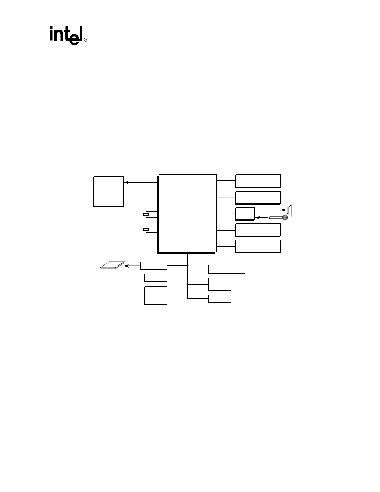
The ARM instruction set is a good target for compilers of many different high-level languages. Where
required for critical code segments, assembly code programming is also straightforward, unlike some RISC
processors that need sophisticated compiler technology to manage complicated instruction interdependencies.
The SA-1110 is a static part and has been designed to run at a reduced voltage to minimize its power
requirements. This makes it a good choice for portable applications where both of these features are
essential.
1.3 Example System
Figure 1-2 s hows how the SA-1110 can be used in a hand held computing device.
Figure 1-2. SA-1110 Example System
Gray Scale
or
Color LCD
Display
3.686
MHz
32.768
KHz
Intel® StrongARM
SA-1110
Portable
Communications
Microcontroller
Introduction
UART
Communications
*
Tablet / Serial
Keyboard
Codec
Infrared
Communications
PCMCIA Interface
(Flash, Modem)
Glue Logic
SRAM
Variable
Latency
I/O
USB Synchronization
Port
SDRAM/DRAM
SMROM/
ROM
Flash
A6701-01
SA-1110 Developer’s Manual 25
Page 26

Introduction
1.4 ARM Architecture
The SA-1110 implements the ARM* V4 architecture as defined in the ARM Architecture
Reference, 28-July-1995, with the following options:
1.4.1 26-Bit Mode
The SA-1110 supports 26-bit mode but all exceptions are initiated in 32-bit mode. The P and D bits
do not affect the operation of SA-1110; they are always read as ones and writes to them are
ignored.
1.4.2 Coprocessors
The SA-1110 s upports MCR and MRC access to coprocessor number 15. These instructions are
used to access the memory-management, configuration, and cache control registers. In addition,
coprocessor 15 provides control for read buffer fills and flushes, and hardware breakpoints. All
other coprocessor instructions cause an undefined instruction exception. N o support for external
coprocessors is provided.
1.4.3 Memory Management
Memory management exceptions preserve the base address registers so that no code is required to
restore state. Separate translation lookaside buffers (TLBs) are implemented for the instruction and
data streams. Each TLB has 32 entries that can each map a segment, a large page, or a small page.
The TLB replacement algorithm is round robin. The data TLBs support both the flush-all and
flush-single-entry operations, while the instruction TLBs support only the flush-all operation.
1.4.4 Instruction Cache
The SA-1110 has a 16 Kbyte instruction cache (Icache) with 32-byte blocks and 32-way
associativity. The cache supports the flush-all function. Replacement is round robin within a set.
The Icache can be enabled while memory management is disabled. When m emory management is
disabled, all memory is considered cacheable by the Icache.
1.4.5 Data Cache
The SA-1110 has an 8 Kbyte data cache (Dcache) with 32-byte blocks and 32-way associativity.
The cache supports the flush-all, flush-entry, and copyback-entry functions. The copyback-all
function is not supported in hardware. This function can be provided by software. The cache is read
allocate with round-robin replacement.
The Dcache has been augmented with a 16-entry, two-way set associative minicache that allocates
when the MMU b and c bits are 0 and 1, respectively. This cache is accessed in parallel with the
main Dcache. Unlike the main data cache, the minicache implements a least-recently-used (LRU)
replacement algorithm. This cache is useful for applications that access large data structures and
would normally thrash the main Dcache. Instead, these data structures can be mapped so that they
allocate into the minicache and only replace data from the same structure.
26 SA-1110 Developer’s Manual
Page 27

1.4.6 Write Buffer
The SA-1110 has an eight-entry write buffer with each entry able to contain 1 to 16 bytes. A drain
write buffer operation is supported.
1.4.7 Read Buffer
The SA-1110 has a four-entry read buffer capable of loading 1, 4, or 8 words of data per entry. This
facility permits software to preload data into the buffer for use at a later time without blocking the
operation of the processor. Software can flush either a single entry or the entire buffer (four
entries). The read buffer is controlled through system control coprocessor 15 and can be enabled
for use in user mode.
Introduction
SA-1110 Developer’s Manual 27
Page 28

Page 29

Functional Description 2
This chapter provides a functional description of the Intel®StrongARM*SA-1110 Microprocessor
(SA-1110). It describes the basic building blocks within the processor, lists and describes the pins,
and explains the memory map.
2.1 Block Diagram
The SA-1110 consists of the following functional blocks:
• ProcessingCore
*
The processor is the ARM
data cache (Dcache). The instruction (I) and data (D) streams are translated through
independent memory-management units (MMUs). Stores are made using a four-line write
buffer. The performance of specialized load routines is enhanced with the four-entry read
buffer that can be used to prefetch data for use at a later time. A 16-entry minicache provides a
smaller and logically separate data cache that can be used to enhance caching performance
when dealing with large data structures.
SA-1 core with a 1 6 Kbyte instruction cache (Icache) and 8 Kbyte
• Memory and PCMCIA Control Module
The memory and PCMCIA control module (MPCM) supports four banks of fast-page-mode
(FPM), extended-data-out (EDO), and/or synchronous DRAM (SDRAM). It also supports up
to six banks of static memory: all six banks allow ROM or Flash memory,each wit h non-burst
or burst read timings. Additionally, the lower three static banks support SRAM, the upper three
static banks support variable latency I/O devices (with the variable data latency controlled by a
shared data ready input), and the lower four static banks support synchronous mask ROM
(SMROM). SMROM is supported only on 32-bit data busses. All other dynamic and static
memory types and variable latency I/O devices are supported on either 16-bit or 32-bit data
busses. Expansion devices are supported through PCMCIA control signals that share the
memory bus data and address lines to complete the card interface. Some external glue logic
(buffers and transceivers) is necessary to implement the interface. Control is provided to
permit two card slots with hot-swap capability.
• Peripheral Control Module
The peripheral control module (PCM) contains a number of serial control devices, an LCD
controller as well as a six-channel DMA controller to provide service to these devices:
– An LCD controller with support for passive or active displays
– A universal serial bus (USB) endpoint controller
– A serial controller with supporting 115 Kbps and 4 Mbps IrDA protocols
– A 16550-like UART supporting 230 Kbps
– A CODEC interface supporting Motorola SPI, National Microwire, TI Synchronous
Serial, or the Phillips UCB1100 and UCB1200 protocol
• System Control Module
The system control module (SCM) is also connected to the peripheral bus. It contains five
blocks used for general system functions:
– A real-time clock (RTC) clocked from an independent 32.768 kHz oscillator
– An operating system timer (OST) for general system timer functions as well as a watchdog
mode
SA-1110 Developer’s Manual 29
Page 30
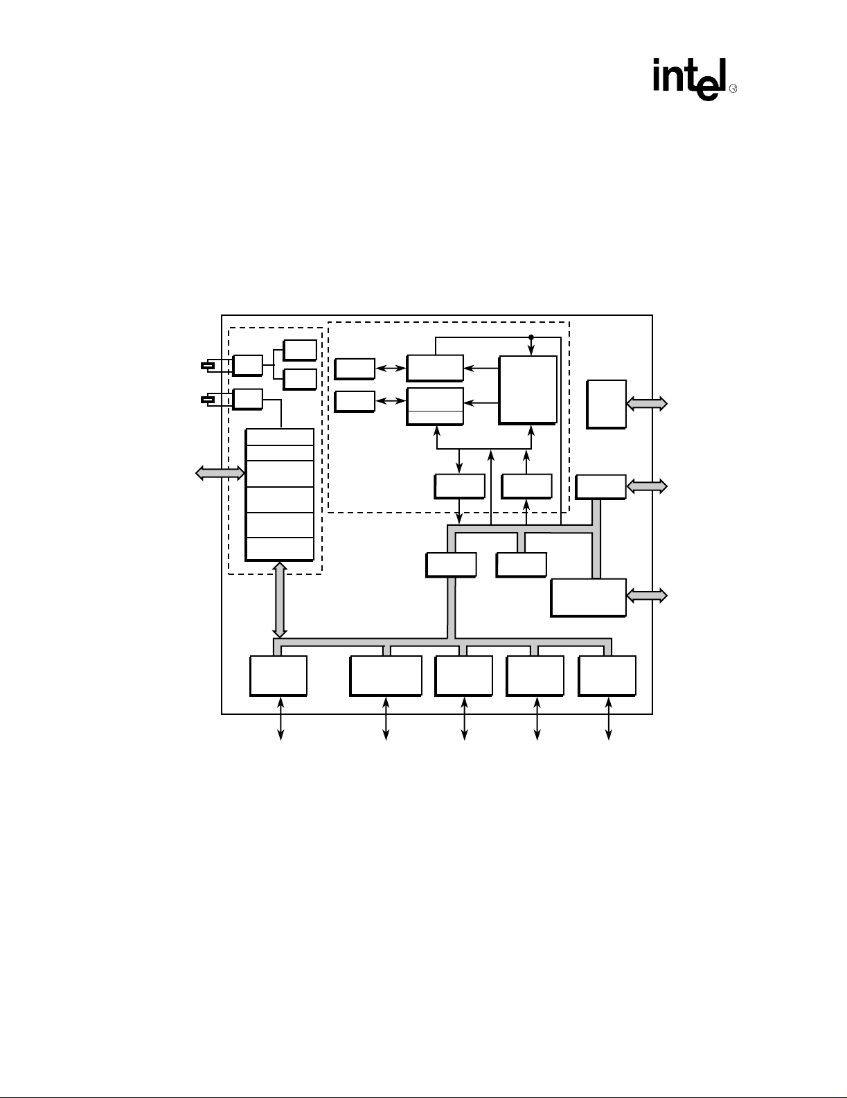
Functional Description
– Twenty-eight general-purpose I/Os (GPIO)
– An interrupt controller
– A power-managementcontroller that handles the transitions in and out of sleep and idle
modes
– A reset controller that handles the various reset sources on the processor
Figure 2-1 shows the functional blocks contained in the SA-1110 integrated processor.
Figure 2-2 is a functional diagram of the SA-111 0.
Figure 2 -1. SA-1110 Block Diagram
3.686
MHz
32.768
KHz
OSC
OSC
PLL1
PLL2
RTC
OS Timer
General-
Purpose I/O
Interrupt
Controller
Power
Management
Reset
Controller
IMMU
DMMU
Icache
(16 Kbytes)
Dcache
(8 Kbytes)
Minicache
System Bus
Instructions
PC
Addr
Load/Store Data
Write
Buffer
Bridge
ARM
SA-1
Core
Read
Buffer
DMA
Controller
Microprocessor
*
Memory and
PCMCIA
Control Module
®
Intel
StrongARM
SA-1110
JTAG
and
Misc
Test
LCD
Controller
*
Peripheral Bus
Serial
Channel 0
UDC
Serial
Channel 1
GPCLK/UART
Serial
Channel 2
IrDA
Serial
Channel 3
UART
Serial
Channel 4
CODEC
A6608-01
30 SA-1110 Developer’s Manual
Page 31

2.2 Inputs/Outputs
Figure 2-2. SA-1110 Functional Diagram
Functional Description
Serial
Channel 0
(USB)
Serial
Channel 1
Serial
Channel 2
(IrDA)
Serial
Channel 3
(UART)
Serial
Channel 4
(CODEC)
Power
Management
Clocks, Reset
and Test
JTAG
UDC-
UDC+
RXD _1
TXD_1
RXD _2
TXD _2
RXD _3
TXD _3
TXD _C
RXD _C
SCLK _C
SFRM _C
BATT_FAULT
VDD_FAULT
PWR_EN
TCK_BYP
TESTCLK
PEXTAL
PXTAL
TEXTAL
TXTAL
nRESET
nRESET_OUT
SMROM_EN
ROM_SEL
TCK
TDI
TDO
TMS
nTRST
®
Intel
StrongARM
SA-1110
[256-pins]
L_DD(7:0)
L_FCLK
L_LCLK
L_PCLK
L_BIAS
GP(27:0)
*
nCAS/DQM(3:0)
nRAS/nSDCS(3:0)
nOE
nWE
nCS(5:0)
RDY
nSDRAS
nSDCAS
SDCKE<1:0>
SDCLK<2:0>
RD/nWR
nPOE
nPWE
nPIOR
nPIOW
nPCE<2:1>
PSKTSEL
nPREG
nPWAIT
nIOIS16
VDD
VDDX
VSS/VSSX
A<25:0>
D<31:0>
LCD
Control
GPIO Ports
Memory
Control
Transceiver
Control
PCMCIA
Bus
Signals
Address
Bus
Data Bus
Supply
A6610-01
SA-1110 Developer’s Manual 31
Page 32

Functional Description
2.3 Signal Description
The following table describes the signals.
KeytoSignalTypes: n– Active low signal
IC – Input, CMOS threshold
ICOCZ – Input, CMOS threshold, output CMOS levels, tristatable
OCZ – Output, CMOS levels, tristatable
Table 2-1. Signal Descriptions (Sheet 1 of 4)
Name Type Description
A[25:0] OCZ Memory address bus. This bus signals the addres s requested for memory
D[31:0] ICOCZ Memory data bus. Bits 15..0 are used for 16-bit data busses.
nCS[5:0] OCZ Static chip s elects. These signals are chip selects to static memory devices such
RDY IC Static data ready signal for nCS[5:3]. This signal should be connected to the data
nOE OCZ Memory output enable. This signal should be connected to the output enables of
nWE OCZ Memory write enable. This signal should be connected to the write enables of
nRAS[3:0]/
nSDCS[3:0]
nCAS[3:0]/
DQM[3:0]
nSDRAS OCZ SDRAM RAS. This signal should be connected to the row address strobe (RAS)
nSDCAS OCZ SDRAM CAS. This signal should be connected to the column address strobe
SDCKE[1:0] OCZ SDRAM and/or SMROM clock enables.
OCZ DRAM RAS or S DRAM CS for banks 0 through 3. These signals should be
OCZ DRAM CAS or SDRAM DQM for data banks 0 through 3. These signals should be
accesses.
Bits 24..10 carry the 15-bit DRAM address. The static memory devices and the
expansion bus receive addres s bits 25..0.
as ROM and F lash. They are individually programmable in the memory
configuration registers. Bits 5..3 c an be used with variable latency I/O devices.
ready output pins of variable latency I/O devices that require variable data
latencies. Devices select ed by nCS[5:3] can share the RDY pin if they drive it high
prior to tristating and a weak external pull-up is present.
memory devices to control their data bus drivers.
memory devices.This signal is us ed in conjunction with nCAS[3:0] to perform byte
writes.
connected to the row address strobe (RAS) pins for asynchronous DRAM or t he
chip select (CS) pins for SDRAM.
connected to the column address strobe (CAS) pins for asynchronous DRAM or
the data output mask enables (DQM) for SDRAM.
pins for all banks of SDRAM.
(CAS) pins for all banks of SDRAM.
SDCKE 0 should be connected to the clock enable (CKE) pins of SMROM.
SDCKE 0 is asserted upon any rest (including sleep-exit) if static memory
bank 0 (boot space) is configured for synchronous mask ROM (SMROM_EN = 1);
otherwise it is deasser ted upon reset.
SDCKE 1 should be connected to the clock enable pins of SDRAM.They ar e
deasserted (held low) during sleep. SDCKE 1 always is deasserted upon reset.
The memory controller provides control register bits for deassertion of each
SDCKE pin. However, SDCKE 0 cannot be deasserted via program if
SMROM_EN =1.
32 SA-1110 Developer’s Manual
Page 33

Table 2-1. Signal Descriptions (Sheet 2 of 4)
Name Type Description
SDCLK[2:0] OCZ SDRAM and/or SMROM clock.
SDCLK 0 should be connected to the clock ( CLK) pins of SMROM.
SDCLK 1 and SDCLK 2 should be connected to the clock pins of SDRAM in bank
pairs 0/1 and 2/3, respectively.They are driven by either the internal memory
controller clock (CPU clock divided by 2) or the memory controller clock divided by
2 (CPU clock divided by 4).
All SDCLK pins are held low during sleep mode and start running at CPU clock
divide by 4 upon any reset (including sleep-exit).
The memory controller provides control register bits for clock division and disable
of each SDCLK pin. However, SDCLK 0 cannot be disabled via program if static
memory bank 0 (boot space) is configured for synchronous mask ROM
(SMROM_EN = 1).
RD/nWR OCZ Read/write direction control for memory and PCMCIA data bus (D[31:0]). T h is
signal is applicable to all memory bus and PCMCIA transfers.
For reads (RD/nWR = 1), system-level bus tran sceivers or directly connected
memory devices should drive D[31:0].
For writes (RD/nWR = 0), the SA-1110 will drive D[31:0].
nPOE OCZ PCMCIA output enable. This signal is an output and is used to perform reads from
memory and attribute space.
nPWE OCZ PCMCIA write enable. This signal is an output and is used to perform writes to
memory and attribute space.
nPIOW OCZ PCMCIA I/O write. This signal is an output and is used to perform write
transactions to the PCMCIA I/O space.
nPIOR OCZ PCMCIA I/O read. This signal is an output and is used to perform read
transactions from the PCMCIA I/O space.
nPCE[2:1] OCZ PCMCIA card enable. These signals are output and are used to select a PCMCIA
card. nPCE 2 enables the high-byte lane and nPCE 1 enables the low-byte lane.
nIOIS16 IC I/OSelect 16. This signal is an input and is an acknowledgment from t he PCM CIA
card that it can perform 16-bit I/O data transfers.
nPWAIT IC PCMCIA wait. This signal is an input and is driven low by the PCMCIA card to
extend the duration of transfers to/from the SA -1110.
PSKTSEL OCZ PCMCIA socket select. This signal is an output and is used by external steering
logic to route control, address, and data signals to one of the PCMCIA sockets.
When PSKTSEL is low, socket zero is selected. When PSKTSEL is high, socket
one is selected. This signal has t he same timing as the address lines.
nPREG OCZ PCMCIA register select. This signal is an output and indicates that, on a memory
transaction, the target address is attribute space. This signal has the same timing
as address.
L_DD[7:0] OCZ LCD controller display data.
L_FCLK OCZ LCD frame clock.
L_LCLK OCZ LCD line clock.
L_PCLK OCZ LCD pixel clock.
L_BIAS OCZ LCD ac bias drive.
TXD_C OCZ CODEC transmit.
RXD_C IC CODEC receive.
Functional Description
SA-1110 Developer’s Manual 33
Page 34

Functional Description
Table 2-1. Signal Descriptions (Sheet 3 of 4)
Name Type Description
SCLK_C OCZ CODEC clock.
SFRM_C OCZ CODEC frame signal.
UDC+ ICOCZ Serial port zero bidirectional, differential signalling pin (UDC).
UDC- ICOCZ Serial port zero bidirectional, differential signalling pin (UDC).
TXD_1 OCZ Serial port one transmit pin (UART).
RXD_1 IC Serial port one receive pin (UART).
TXD_2 OCZ Serial port two transmit pin (IrDA).
RXD_2 IC Serial port two receive pin (IrDA).
TXD_3 OCZ Serial port three transmit pin (UART).
RXD_3 IC Serial port three receive pin (UART).
GP[27:0] ICOCZ General-purpose input output.
SMROM_EN IC Synchronous mask ROM (SMROM) enable. This pin is used to determine if the
ROM_SEL IC ROM select. This pin is used to configure the ROM width. It is either grounded or
PXTAL IC Input connection for 3.686-MHz crystal (non-CMOS threshold).
PEXTAL OCZ Output connection for 3.686-MHz crystal (non-CMOS level).
TXTAL IC Input connection for 32.768-kHz crystal (non-CMOS threshold).
TEXTAL OCZ Output connection for 32.768-kHz crystal (non-CMOS level).
PWR_EN OCZ Power enable. Active high. PWR_EN enables the external VDD power supply.
BATT_FAULT IC Battery fault. Signals the SA-1110 that the main power source is going away
VDD_FAULT IC VDD fault. Signals the SA-1110 that the main power supply is going out of
nRESET IC Hard reset. This active low signal is a level-sensitive input used to start th e
nRESET_OUT OCZ Reset out. This signal is asserted when nRESET is asserted and deasserts when
nTRST IC Test interface reset. Note this pin has an internal pull-down resistor and must be
boot ROM (static memory bank 0) is async h ronous or synchronous. If
asynchronous, boot ROM is selected (SMROM_EN = 0) and its width is
determined by the state of the ROM_SEL pin. SMROM is supported only on 32-bit
data busses.
pulled high. If ROM_SEL is grounded, the ROM width is 16 bits. If ROM_SEL is
pulled up, the ROM width is 32 bits.
Deasserting it signals the power supply that the syst em is going into sleep mode
and that the VDD power supply should be removed.
(battery is low or has been removed from the system). The assertion of
BATT_FAULT causes the SA-1110 to enter sleep mode. The SA-1110 will not
recognize a wake-up event while this signal is asserted.
regulation (shorted card is inserted). VDD_FAULT will cause the SA-1110to enter
sleep mode. VDD_FAULTis ignored after a wake-up event until the power supply
timer completes (approximately 10 ms).
processor from a known address. A low level will cause the c u rrent instruction to
terminate abnormally, and the on-chip caches, MMU , and write buffer to be
disabled.
When nRESET is driven high, the processor will restart from address 0. nRESET
must remain low until the power supply is stable and the internal 3.686-MHz
oscillator has come up to speed. While nRESET is low, the processor will perform
idle cycles.
the processor has completed resetting. nRESET_OUT is also asserted for " soft"
reset events (sleep and watchdog).
driven high to enable the JTAG circuitry. If left unconnected, this pin is pulled low
and disables JTAG operation.
34 SA-1110 Developer’s Manual
Page 35

Table 2-1. Signal Descriptions (Sheet 4 of 4)
Name Type Description
TDI IC JTAG test interface data input. Note this pin has an internal pull-up resistor.
TDO OCZ JTAGtest interface data out put . Note this pin does not have an internal pull-up
resistor.
TMS IC JTAG test interface mode select. Note this pin has an internal pull-up resistor.
TCK IC JTAGtest interface reference clock. This times all the transfers on the JTAG test
interface. Note this pin has an internal pull-down resistor.
TCK_BYP IC Test clock PLL bypass. When TCK_BYP is high, the TESTCLK is used as the
core clock in place of the PLL clock; when low, the internal PLL output is used.
This signal has no relation to the JTAG TCK pin.
TESTCLK IC Test clock. TESTCLK is used to provide the core clock when TCK_BYP is high. It
should be tied low if TCK_BYP is low. This pin should be used for test purposes
only.An end user should ground this pin.
VDD — Positive supply for the core. Nine pins are allocated to this supply; eight pins are
labeled VDD. The ninth pin, labeled VDDP is dedicated to the PLL supply and
should have its own dedicat ed decoupling capacitor.Also, it should be tied directly
to the VDD power plane with the other eight VDD pins.
VDDX — Positive supply for the pins. See Chapter 14 for a count of VDDX pins. All of the
pins allocated to VDDX (labeled VDDX1, VDDX2, and V DDX3) should be tied
directly to the VDDX power plane and are all required to remain powered up at all
times for proper device operation. VDDX3 is connected to an internal voltage
regulator and should have its own dedicated decoupling capacitor.
VSS — Ground supply. Nine pins are allocated to VSS, including one for the PLL.
VSSX — Ground supply for the I/O pins. See Chapter 14, “Package and Pinout,” for a count
of VSSX pins.
Functional Description
SA-1110 Developer’s Manual 35
Page 36

Functional Description
2.4 Memory Map
Figure 2-3 shows the SA-1110 memory map. The map is divided into four main partitions of
1 Gbyte each.
• Physical address: 0h0000 0000 to 0h3FFF FFFF.
This partition is dedicated to static memory devices (ROM, SRAM, and Flash) and to the
PCMCIA expansion bus area. This space is divided into:
— Four 128 Mbyte blocks for static memory devices
The static memory space is intended for ROM, SRAM, and Flash memory. The bottom
partition (at 0h0000 0000) is assumed to be ROM at boot time. The SMROM_EN pin is
used to determine if the boot ROM is asynchronous or synchronous. If asynchronous,
boot ROM is selected (SMROM_EN = 0), its width (16-bit or 32-bit) is determined by the
state of the ROM_SEL pin. SMROM is supported only on 32-bit data busses.
Note: The upper 64MBytes of each 128MByte static bank select cannot be acces sed
because only 26 bits of the physical address are available on external pins. Attempts to
accesses any static bank selects upper 64Mbyte will actually cause an access to that bank
selects lower 64MByte, because the missing (27th) physical address bit is ignored.
— Two 256 Mbyte blocks for the PCMCIA interface
The PCMCIA interface is divided into Socket 0 and Socket 1 space. These partitions are
further subdivided into I/O, memory and attribute space.
• Physical address: 0h4000 0000 to 0h7FFF FFFF
This partition includes:
— Two 128 Mbyte blocks for static memory or variable latency I/O devices. This block
differs from the other three status memory spaces because it can be used for variable
latency I/O but not SRAM.
Note: The upper 64MBytes of each 128MByte static bank select cannot be acces sed
because only 26 bits of the physical address are available on external pins. Attempts to
accesses any static bank selects upper 64Mbyte will actually cause an access to that bank
selects lower 64MByte, because the missing (27th) physical address bit is ignored.
— One 768 Mbyte block of reserved space. Accessing this reserved space results in a data
abort exception.
• Physical address: 0h8000 0000 to 0hBFFF FFFF
This partition contains all on-chip registers (except those specified by the ARM V4
architecture). This block is further divided into four 256 Mbyte blocks that contain control
registers for the following major functional blocks within the processor:
— Peripheral Control Module Registers
— System Control Module Registers
— Memory and Expansion Registers
— LCD and DMA Registers
• Physical address: 0hC000 0000 to 0hFFFF FFFF
This partition contains DRAM memory and is divided into:
— Four banks of DRAM fixed at 128 Mbyte each. With multiple banks implemented, there
probably will be gaps in the map that should be mapped through the
memory-management unit.
36 SA-1110 Developer’s Manual
Page 37

Functional Description
— One 128 Mbyte block that is mapped within the memory controller and returns zeros
when read. This function is intended to facilitate rapid cache f lushing by n ot requiring an
external memory access to load data into the cache. This space is burstable. Writes to this
space have no effect.
— One 384 Mbyte block of reserved space. Accessing this reserved space results in a data
abort exception.
SA-1110 Developer’s Manual 37
Page 38

Functional Description
Figure 2-3. SA-1110 Memory Map
Reserved (384 Mbytes)
Zeros Bank (128 Mbytes)
DRAM Bank 3 (128 Mbytes)
Cache flush replacement data.
Reads return zero
128 Mbytes
0hC000 0000
0h8000 0000
0h5000 0000
0h4000 0000
0h2000 0000
0h0000 0000
DRAM Bank 2 (128 Mbytes)
DRAM Bank 1 (128 Mbytes)
DRAM Bank 0 (128 Mbytes)
LCD and DMA Registers
(256 Mbytes)
Memory and Expansion Registers
(256 Mbytes)
System Control Module Registers
(256 Mbytes)
Peripheral Control Module Registers
(256 Mbytes)
Reserved (768 Mbytes)
Static Bank Select 5 (128 Mbytes)
Static Bank Select 4 (128 Mbytes)
PCMCIA Socket 1 Space
(256 Mbytes)
PCMCIA Socket 0 Space
(256 Mbytes)
Static Bank Select 3 (128 Mbytes)
Static Bank Select 2 (128 Mbytes)
Static Bank Select 1 (128 Mbytes)
Static Bank Select 0 (128 Mbytes)
Dynamic Memory Interface
512 Mbytes
Internal Registers
1 Gbyte
Static Memory or Variable
Latency I/O Interface
256 Mbytes
PCMCIA Interface
512 Mbytes
Variable Latency I/O Interface
128 Mbytes
Static Memory Interface
(ROM, Flash, SRAM)
512 Mbytes
A9080-01
Note: The upper 64MBytes of each 128MByte static bank select cannot be accessed because only 26 bits
of the physical address are available on external pins. Attempts to accesses any static bank selects
upper 64Mbyte will actually cause an access to that bank s elects lower 64MByte, because the
missing (27th) physical address bit is ignored.
38 SA-1110 Developer’s Manual
Page 39

ARM Implementation Options 3
The following sections describe ARM*architecture options that are implemented by the
®
StrongARM*SA-1110 Microprocessor (SA-1110).
Intel
3.1 Big and Little Endian
Note: The Big Endian implementation scheme is not supported in t he B4 stepping and above.
The big endian bit in the control register set s whether the SA-1110 treats words stored in memory
as being stored in big endian or little endian format. Memory is viewed as a linear collection of
bytes numbered upwards from 0. Bytes 0 to 3 hold the first stored word, bytes 4 to 7 hold the
second, and so on.
In the little endian scheme, the lowest numbered byte in a word is considered to be the least
significant byte of the word and the highest numbered byte is the most significant. Byte 0 of the
memory system should be connected to data lines 7 through 0 (D[7:0]) in this scheme.
In the big endian scheme, the most significant byte of a word is stored at the lowest numbered byte
and the least significant byte is stored at the highest numbered byte. Therefore, byte 0 of the
memory system should be connected to data lines 31 through 24 (D[31:24]).
The state of the big endian bit changes the location of the bytes only within a 32-bit word. The
accessed bytes are changed for the load byte, store byte, load halfword, and store halfword
instructions only. Instruction fetches and word load and stores are not changed by the state of the
big endian bit, except when those accesses are performed with memory on 16-bit busses. See
Chapter 10, “Memory and PC-Card Control Module” for d etails on configuring data bus widths for
various memory types.
These conventions are identical to those of the SA-110. In addition, the SA-1110 DMA controller
is programmable by channel as to the endian format of the transfer. For DMA transfers, all memory
accesses are words. Then the data is buffered and transferred to/from the device as halfwords or
bytes. When the words are assembled or disassembled, the endian format of the channel is
observed. For details on how DMA data is transferred relative to the endian format of the channel,
see the Section 11.6, “DMA Controller” on page 11-210in Chapter 11, “Peripheral Control
Module”.
3.2 Exceptions
Exceptions arise whenever there is a need for the normal flow of program execution to be broken;
for example, so that the processor can be diverted to handle an interrupt from a peripheral. The
processor state just prior to handling the exception must be preserved so that the original program
resumes when the exception routine has completed. Many exceptions may arise at the same time.
The SA-1110 handles exceptions by making use of banked registers to save state. The contents of
PC and CPSR are copied into the appropriate R14 and SPSR, and the PC and mode bits in the
CPSR bits are forced to a value that depends on the exception.
SA-1110 Developer’s Manual 39
Page 40

ARM Implementation Options
Interrupt disable flags are set where required to prevent otherwise unmanageable nestings of
exceptions. In the case of a reentrant interrupt handler, R14 and the SPSR should be saved onto a
stack in main memory before reenabling the interrupt; when transferring the SPSR register to and
from a stack, it is important to transfer the whole 32-bit value, and not just the flag or control fields.
When multiple exceptions arise simultaneously,a fixed priority determines the order in which they
are handled. The priorities are listed later in this chapter. Most exceptions are fully defined in the
ARM Architectural Reference. The following sections specify the exceptions where the SA-1110
implementation differs from the ARM Architectural Reference.
SA-1110initiates all exceptions in 32-bit mode. When an exception occurs while running in 26-bit
mode, the SA-1110 saves only t he PC in R14 and the CPSR in the SPSR of the exception mode.
The 32-bit handler must merge the condition codes, the interrupt enables, and the mode from the
SPSR into R14 if a handler is to run in 26-bit mode.
3.2.1 Power-Up Reset
When the nRESET signal is low, SA-1110 stops executing instructions, asserts the nRESET_OUT
pin, and then performs idle cycles on the bus.
When nRESET is high again, SA-1110 does the following:
1. O verwrites R14_svc and SPSR_svc by copying the current values of the PC and CPSR into
them. The values of the saved PC and CPSR are not defined.
2. Forces M 4:0 =10011 (32-bit supervisor mode) and sets the I and F bits in the CPSR.
3. F orces the PC to fetch the next instruction from address 0x0000 0000.
4. Based on the state of the ROM_SEL pin, fetches this first instruction from either 16-bit
(ROM_SEL low) or 32-bit (ROM_SEL high) space. The SA-1110 memory controller
assembles the data into words in the case of a 16-bit wide ROM.
At the end of the reset sequence, the MMU, Icache, Dcache, and write buffer are disabled.
Alignment faults are also disabled, and little- endian mode is enabled. During power-up, nRESET
must be negated no earlier than 150 milliseconds after VDD and VDDx are stable to allow the
internal 3.686-MHz oscillator to stabilize. After the negation of nRESET, the PLL begins its
internally timed locking sequence. Note that the assertion of nRESET is destructive because the
state of the real-time clock and the contents of DRAM are lost.
The SA-1110 has three types of reset. See Section 1 6.2, “Reset” on page 16-414 in the
Boundary-Scan Test Interface for details.
3.2.2 ROM Size Select
The ROM width may be selected using the ROM_SEL pin. This pin is sampled during the assertion
of nRESET. The value is stored in the memory controller for use during ROM accesses. If this
signal is high during RESET, then the ROM is selected to be 32 bits wide. If it is low during
RESET, then the ROM width is 16 bits. There is no provision for 8-bit ROMs in the SA-1110.
40 SA-1110 Developer’s Manual
Page 41

3.2.3 Abort
An abort can be signalled by the internal memory-management unit, through a data breakpoint, or
by a reference to reserved memory. An abort indicates that the current memory access cannot be
completed or that a prespecified breakpoint address and (optionally) data pattern has been reached.
For instance, in a virtual memory s ystem, the data corresponding to the current address may have
been moved out of memory onto a disk, and considerable processor activity may be required to
recover the data before the access can be performed successfully.The SA-1110 checks for an abort
during memory access cycles. When aborted, the SA-1110 responds in one of two ways:
1. If the abort occurred during an instruction prefetch (a prefetch abort), the prefetched
instruction is marked as invalid but the abort exception does not occur immediately. If the
instruction is not executed, for example, as a result of a branch being taken while it is in the
pipeline, no abort will occur. An abort will take place if the instruction reaches the head of the
pipeline and is about to be executed.
2. If the abort occurred during a data access (a data abort), the action depends on the instruction
type.
a. Single data transfer instructions (LDR, STR) will abort with no registers modified.
b. The swap instruction (SWP) is aborted as though it had not executed, though externally
c. Block data transfer instructions (LDM, STM) abort on the first access that cannot
ARM Implementation Options
the read access may take place.
complete. If write-back is set, the base is NOT updated. If the instruction would normally
have overwritten the base with data (for example, an LDM instruction with the base in the
transfer list), the original value in the base register is restored.
When either a prefetch or data abort occurs, the SA-1110 performs the following:
1. Saves the address of the aborted instruction plus 4 (for prefetch aborts) or 8 (for data aborts) in
R14_abt; saves CPSR in SPSR_abt.
2. Forces M 4:0 =10111 (abort mode) and sets the I bit in the CPSR.
3. Forces the PC to fetch the next instruction from either address 0x0C (prefetch abort) or address
0x10 (data abort).
To return after fixing the reason for the abort, use SUBS PC,R14_abt,#4 (for a prefetch abort) or
SUBS PC,R14_abt,#8 (for a data abort). This will restore both the PC and the CPSR, and retry t he
aborted instruction.
The abort mechanism allows a demand paged virtual memory system to be implemented when
suitable memory management software is available. The processor is allowed to generate arbitrary
addresses, and when the data at an address is unavailable, the MMU signals an abort. The processor
traps into system software, which must work out the cause of the abort, make the requested data
available, and retry the aborted instruction. The application program needs no knowledge of the
amount of memory available to it, nor is its state in any way affected by the abort.
SA-1110 Developer’s Manual 41
Page 42

ARM Implementation Options
3.2.4 Vector S ummary
Table 3-1 lists byte addresses, and they normally contain branch instructions pointing to the
relevant routines. These addresses (except the reset v ector) can be changed (to 0xFFFF xxxx)
through the vector adjust facility (bit 13, register 1, coprocessor 15). The vector adjust is cleared at
reset and cannot modify the reset vector.
Table 3-1. Vector Summary
Address Exception Mode on Entry
0x00000000 Reset Supervisor
0x00000004 Undefined instruction Undefined
0x00000008 Software interrupt Super visor
0x0000000C Abort (prefetch) Abort
0x00000010 Abort (data) Abort
0x00000014 Not used —
0x00000018 IRQ IRQ
0x0000001C FIQ FIQ
3.2.5 Exception Priorities
When multiple exceptions arise at the same time, a fixed priority system determines the order in
which they will be handled:
1. Reset (highest priority)
2. D ata abort
3. FIQ
4. IRQ
5. P r efetch abort
6. Undefined instruction, software interrupt (lowest priority)
Note that not all exceptions can occur at once. Undefined instructions and software interrupts are
mutually exclusive because they correspond to particular (nonoverlapping) decodings of the
current instruction.
If a data abort occurs at the same time as a FIQ, and FIQs are enabled (that is, the F flag in the
CPSR is clear), the SA-1110 will enter the data abort handler and then immediately proceed to the
FIQ vector. A normal return from FIQ will cause the data abort h andler to resume execution.
Placing data abort at a higher priority than FIQ is necessary to ensure that the transfer error does
not escape detection; the t ime for this exception entry should be added to worst-case FIQ latency
calculations.
42 SA-1110 Developer’s Manual
Page 43

3.2.6 Interrupt Latencies and Enable Timing
The ability to recognize an IRQ or FIQ interrupt is, in part, determined by the I and F bits of the
CPSR. To ensure that a pending interrupt is taken, an interrupt-enabling write to CPSR (msr
instruction) must be separated from an interrupt-disabling write to the CPSR by at least two
instructions.
3.3 Coprocessors
The SA-1110 has no external coprocessor bus, so it is not possible to add external coprocessors to
this device.
The SA-1110uses the internal coprocessor designated 15 for control of the on-chip MMU, caches,
clocks, and breakpoints. Coprocessor 15 is also used for read-buffer fills and flushes. If a
coprocessor other than 15 is used, then the SA-1110 will take the undefined instruction trap. The
coprocessor load, store, and data operation instructions also take the undefined instruction trap.
Permissions are set so that access to coprocessor 15 is privileged except where protection is
programmable with respect to the read buffer operations.
Note: The write buffer must be flushed prior to loading the read buffer to maintain coherency between the
two buffers. But, if user-mode MCR access is enabled for the read buffer and the flush is attempted
while in user mode, an undefined instruction exception will occur. In this case, the exception
handler must perform the write buffer flush, then return to user mode to execute the read buffer
load. Alternatively, an SWI instruction can be used as a service call to flush the write buffer.
ARM Implementation Options
SA-1110 Developer’s Manual 43
Page 44

Page 45

Instruction Set 4
This section describes the instruction timing for the Intel®StrongARM*SA-1110 Microprocessor
(SA-1110).
4.1 Instruction Set
The SA-1110implements the ARM*V4 architecture as defined in the ARM Architecture R eference,
28-July-1995, with previously noted options and additions.
4.2 Instruction Timing
Table 4-1 lists the instruction timing for the SA-1110. The result delay is the number of cycles that
the next sequential instruction would stall if it used the result as an input. The issue cycles are the
number of cycles that this instruction takes to issue. For most instructions, the result delay is zero
and the issue cycles is one. For load and stores, the timing is for cache hits.
Table 4-1. Instruction Timing
Instruction Group Result Delay Issue Cycles
Data processing 0 1
Mul or Mul/Add giving 32-bit result 1..3 1
Mul or Mul/Add giving 64-bit result 1..3 2
Load single – write-bac k of base 0 1
Load single – load data zer o extended 1 1
Load single – load data sign extended 2 1
Store single – write-back of base 0 1
Load multiple (delay for last register) 1
Store multiple – write-back of base 0
Branch or branch and link 0 1
MCR 2 1
MRC 1 1
MSR to control 0 3
MRS 0 1
Swap 2 2
MAX
(2, number of re gisters loaded)
MAX
(2, number of re gisters loaded)
SA-1110 Developer’s Manual 45
Page 46

Page 47

Caches, Write Buffer, and Read Buffer 5
To reduce effective memory access time, the Intel®StrongARM*SA-1110 Microprocessor
(SA-1110) has an instruction cache, a data cache, a write buffer, and a read buffer. All except the
read buffer are transparent to program execution. The following sections describe each of these
units and give all necessary programming information.
5.1 Instruction Cache (Icache)
The SA-1110 contains a 16 Kbyte instruction cache (Icache). The Icache has 512 lines of 32 bytes
(8 words), arranged as a 32-way set associative cache, and uses the virtual addresses generated by
the processor core. The Icache is always reloaded a line at a time (8 words). It may be enabled or
disabled via the SA-1110 control register, and is disabled on the assertion of nRESET or through a
software or sleep reset sequence. (See Chapter 9, “System Control Module” for details.) The
operation of the cache, when memory management is enabled, is further controlled by the
cacheable or C bit stored in the memory-management page table. If memory management is
disabled, all addresses are marked as cacheable (C=1). When memory management is enabled, the
C bit in each page table entry can disable caching for an area of virtual memory.
5.1.1 Icache Operation
In the SA-1110, the instruction cache is searched regardless of the state of the C bit; only reads that
miss the cache are affected. If, on an Icache miss, the C bit is a one or the Memory Management
Unit (MMU) is disabled, a line fetch of 8 words is performed and it is placed in a cache bank with
a round-robin replacement algorithm. If, on a miss, the MMU is enabled and the C bit is a zero for
the given virtual address, an external memory access for a single word is performed and the cache
is not written.The Icache should be enabled as soon as possible after reset for best performance.
5.1.2 Icache Validity
The Icache operates with virtual addresses, so care must be taken to ensure that its contents remain
consistent with the virtual-to-physical mappings performed by the memory management u nit. If the
memory mappings are changed, the Icache validity must be ensured. The Icache is not coherent
with stores to memory, so programs that write cacheable instruction locations must ensure the
Icache validity. Instruction fetches do not check the write buffer, so data must not only be pushed
out of the cache but the write buffer must also be drained.
5.1.2.1 Software Icache Flush
The entire Icache can be invalidated by writing to the SA-1110 cache operations register (register
7). The cache is flushed immediately when the register is written, but note that the following
instruction fetches may come from the cache before the register is written.
SA-1110 Developer’s Manual 47
Page 48

Caches, Write Buffer, and Read Buffer
5.1.3 Icache Enable/Disable and Reset
The Icache is automatically disabled and flushed on the assertion of nRESET. Once enabled,
cacheable read accesses cause lines to be placed in the cache. If the Icache is subsequently
disabled, no new lines are placed in the cache, but the cache is still searched and if the data is
found, it will be used by the processor. If the data in the cache must not be used, then the cache
must be flushed.
5.1.3.1 Enabling the Icache
To enable the Icache, set bit 12 in the control register. The MMU and Icache may be enabled
simultaneously with a single control register write.
5.1.3.2 Disabling the Icache
To disable the Icache, clear bit 12 in the control r egister.
5.2 Data Caches (Dcaches)
The SA-1110 contains two logically separate data caches: the main data cache and the mini data
cache (or minicache). The main data cache, an 8 Kbyte write-back Dcache, has 256 lines of 32
bytes (8words) in a 32-way set-associative organization. It is intended for use during most data
accesses. This cache allocates on loads to spaces marked B=1 and C=1. Replacements in the main
data cache are selected according to a set of round-robin pointers. At reset, the pointer in each
block of the Dcache points to way zero of each 32-way block. As lines are allocated, the pointers
are incremented to the next way of the set. After way 31 is allocated, the next line fill replaces (and
copies back to memory, if dirty) the data in way zero. The m inicache is a 512-byte write-back
cache. It has 16 lines of 32 bytes (8 words) in a two-way set-associative organization and provides
an alternate caching structure for dealing with large data structures that could thrash the main data
cache. This cache allocates on loads to spaces marked B=0 and C=1. Unlike the main data cache,
the minicache implements a least-recently-used (LRU) replacement algorithm.
The Dcaches are accessed in parallel and the design ensures that a p articul ar line entry will exist in
only one of the two at any time. Both Dcaches use the virtual address generated by the processor
and allocate only on loads (write misses never allocate in the cache). Each line entry contains the
physical address of the line and two dirty bits. The dirty bits indicate the status of the first and the
second halves of the line. When a store hits in the Dcaches, the dirty bit associated with it is set.
When a line is evicted from the Dcaches, the dirty bits are used to decide if all, half, or none of the
line will be written back to memory using the physical address stored with the line. The Dcaches
are always reloaded a line at a time (8 words).
The Dcaches allocate only on loads and according to the settings of the B and C bits in the MMU.
If B=0 and C=1, the memory access allocates into the minicache. If B=1 and C=1, the memory
access allocates into the main data cache. The Dcaches should be flushed prior to changing the
bufferable and/or cacheable state of the page table mapping.
The main data cache and the minicache are enabled and disabled via the SA-1110 control register,
and are disabled on nRESET as well as software, sleep, and watchdog reset. The operation of the
Dcaches is further controlled by the cacheable or C bit and the bufferable or B bit stored in the
memory-management page table. For this reason, to use the Dcaches, the MMU must be enabled.
The two functions may be enabled simultaneously with a single write to the control register.
48 SA-1110 Developer’s Manual
Page 49

Note: The Dcaches operate with virtual addresses, so care must be taken to ensure that their contents
remain consistent with the virtual-to-physical mappings performed by the memory-management
unit. If the memory mappings are changed, the validity of the Dcaches must be ensured.
5.2.1 Cacheable Bit – C
The cacheable bit determines whether, on load misses, the data being read should be placed in one
of the two data caches. Cache hits are not affected by the cacheable bit; if a data access hits in the
cache, the data is assumed to be valid and the load or store is p erformed. Typically, main m emory i s
marked as cacheable to improve system performance and I/O space as noncacheable to stop the
data from being stored in SA-1110's cache. For example, if the processor is polling a hardware flag
in I/O space, it is important that the processor is forced to read data from the external peripheral,
and not a copy of initial data held in the cache.
5.2.1.1 Cacheable Reads – C=1
A linefetch of 8 words will be performed and it wi ll be placed in a cache b ank with a round-robin
replacement algorithm.
5.2.1.2 Noncacheable Reads – C=0
Caches, Write Buffer, and Read Buffer
An external memory access will be performed and the cache will not be written.
5.2.2 Bufferable Bit – B
The bufferable bit does not affect writes that hit the Dcaches. If a store hits i n the Dcaches, the s tore
is assumed to be bufferable. Write-backs of dirty lines are treated as bufferable writes. See the
Section 5.3, “Write Buffer (WB)” on page 5-51 for more information on the B bit.
Table 5-1 summarizes the effects of the B and C bits on the Dcaches.
T a ble 5-1. Effects of the Cacheable and Bufferable Bits on the Data Caches
Load Store
BC
0 0 Deliver cache data. Load from memo ry.
0 1 Deliver cache data. Allocate to minicache. Store to either cache.
1 0 Deliver cache data. Load from memo ry.
1 1 Deliver cache data. Allocate to main data cache. Store to either cache.
Cache Hit Cache Miss Cache Hit Cache Miss
– No allocate.
– No allocate.
Store to either cache.
– Mark line dirty.
– Mark line dirty.
Store to either cache.
– Mark line dirty.
– Mark line dirty.
Store to memory.
– No allocate.
Store to memory.
– No allocate.
Store to memory.
– No allocate.
Store to memory.
– No allocate.
SA-1110 Developer’s Manual 49
Page 50

Caches, Write Buffer, and Read Buffer
5.2.3 Software Dcache Flush
The SA-1110 supports the flush and clean operations on single entries of the Dcaches by writes to
the cache operations registers. The flush whole cache is also supported. Note that since this is a
write-back cache, to prevent the loss of data, a flush whole must be preceded by a sequence of
loads to cause the cache to write back any dirty entries. The memory controller in the SA-1110
provides an internally decoded memory space to perform coherent Dcache flushing. This space
resides in the upper 512 megabytes of the memory map (starting at virtual address
0hE000 0000) and, when accessed, is detected by the memory controller, which then returns zeros
without incurring an external memory latency.
The following code causes the main data cache to flush all dirty entries:
;+
;Call:
; R0 points to the start of a 8192 byte region of readable data used
; only for t his cache flushing routine.
;blwriteBackDC
;Return:
; R0, R1, R2 trashed
; Data cache is c lea n
;-
writeBackDC
movr0, 0hE0000000
addr1, r0, #8192
l1
ldr r2, r0, #32
teqr1, r0
bnel1
mcrp15, 0, r0, c7, c6, 0
movpc, r14
A similar routine may be written to flush the minicache. To perform this flush, the MMU B and C
settings must be as described above. The invalidate-all operation also invalidates the minicache.
5.2.3.1 Doubly Mapped Space
Since the Dcaches work with virtual addresses, it is assumed that every virtual address maps to a
different physical address. If the same physical location is accessed by more than one virtual
address, the cache cannot maintain consistency, since each virtual address has a separate entry in
the cache, and only one entry is updated on a processor write operation. To avoid any cache
inconsistencies, doubly mapped virtual addresses should be m arked as noncacheable.
5.2.4 Dcaches Enable/Disable and Reset
The Dcaches are automatically disabled and f lushed on the assertion of nRESET. Once enabled,
cacheable read accesses cause lines to be placed in the Dcaches. If subsequently disabled, no new
lines are placed in the Dcaches, but they are still searched and if the data is found, it is used by the
processor. Write operations continue to update the Dcaches, thus m aint aining consistency with the
external memory. If the data in the Dcaches must not be used, then the Dcaches must be flushed.
50 SA-1110 Developer’s Manual
Page 51

5.2.4.1 Enabling the Dcaches
To enable the Dcaches, make sure that the MMU is enabled first by setting bit 0 in the control
register,then enable the Dcaches by s e tting bit 2 in the control register. The MMU and Dcaches can
be enabled simultaneously with a single control register write.
5.2.4.2 Disabling the Dcaches
To disable t he Dcache, clear bit 2 in the control register.
5.3 Write Buffer (WB)
The SA-1110 write buffer is used to improve system performance by buffering up to 8 blocks of
data of 1 to 16 bytes, at independent addresses. It can be enabled or disabled via the W bit (bit 3) in
the SA-1110 control register. The buffer is disabled and all entries are marked empty fol lowing
reset. Operation of the write buffer is further controlled by the cacheable or C bit and the
bufferable or B bit, which are stored in the memory-management page tables. For this reason, to
use the write buffer, the MMU must be enabled. The two functions can be enabled simultaneously
with a single write to the control register. For a write to use the write buffer, both the W bit in the
control register and the B bit in the corresponding page table must b e set. It is not possible to abort
buffered writes externally. Stores will not merge with other data at the same line address in the
write buffer with the exception of store multiples, which do merge.
Caches, Write Buffer, and Read Buffer
5.3.1 Bufferable Bit
This bit controls whether a write operation may use the write buffer. Typically, main memory is
bufferable and I/O space unbufferable.
5.3.2 Write Buffer Operation
When the CPU performs a store, the Dcaches are first checked. If one of the Dcaches hits on the
store and the protection for the location and mode of the store allows the write, then the write
completes in the Dcaches and the write buffer is not used. If the location misses in the Dcaches,
then the translation entry for that address is inspected and the state of the B and C bits determines
which of the three following actions are performed. If the write buffer is disabled via the SA-1110
control register, writes are treated as if the B bit is a zero.
5.3.2.1 Writes to a Bufferable and Cacheable Location (B=1,C=1)
If the write buffer is enabled and the processor performs a write to a bufferable and cacheable
location, and the data is in one of the caches, then the data is written to that cache, and the cache
line is marked dirty. If a write to a bufferable area misses in both data caches, the data is placed in
the write buffer and the CPU continues execution. The write buffer performs the external write
sometime later. If a write is performed and the write buffer is full, then the processor is stalled until
there is sufficient space in the buffer. No write buffer merging is allowed in the SA-1110 except
during store multiples.
SA-1110 Developer’s Manual 51
Page 52

Caches, Write Buffer, and Read Buffer
5.3.2.2 Writes to a Bufferable and Noncacheable Location (B=1,C=0)
If the write buffer is enabled and the processor performs a write to a bufferable but noncacheable
location and misses in the Dcaches, the data is placed in the write buffer and the C PU continues
execution. The write buffer performs the external write sometime later. Store multiples are not
merged in the write buffer when B = 1, C = 0.
5.3.2.3 Unbufferable and Noncacheable Writes (B=0, C=0)
If the write buffer is disabled or the CPU performs a write to an unbufferable area, the processor is
stalled until the write buffer empties and the write completes externally. This requires several
external clock cycles.
5.3.2.4 Writes to a Non-Bufferable and Cacheable Location (B=0, C=1)
When store multiples occur to a page that is cacheable but not b uffereable (B=0,C=1), the write
data will be merged into the write buffer and burst writes will occur to memory.
5.3.3 Enabling the Write Buffer
To enable the write buffer, ensure that the MMU is enabled by setting bit 0 in the control register,
then enable the write buffer by setting bit 3 in the control regis ter. The MMU and write buffer can
be enabled simultaneously with a single write to the control register.
5.3.3.1 Disabling the Write Buffer
Todisable the write buffer,clear bit 3 in the control register. Any writes already in the write buffer
will complete normally,but a drain write buffer needs to be done to force all writes out to memory.
Note: The write buffer is used to hold dirty copy-back cached lines from the data cache. It must be
enabled along with the data cache.
5.4 Read Buffer (RB)
The SA-1110 contains a software-programmable read buffer that can increase the performance of
critical loop code by prefetching data. The RB enables the preallocation of read-only data into one
of four 32-byte buffers without stalling the pipe. For subsequent loads that hit in the RB, data is
sourced from the buffer instead of the Dcaches at a rate of 1 word per core clock (as long as the
load address hits in the TLB of the DMMU). Also, because the programmer specifies which entry
of the RB is used, critical data can be “locked” in to eliminate bus latency.
The RB is controlled using coprocessor 15, register 9, and provides the capability to allocate 1
word, a half-line (4 words), or a full line (8 words) into one of four entries of the RB. (See
Chapter 6, “Coprocessors” for a detailed RB coprocessor description.) Half-line loads are
automatically aligned onto half-block boundaries (the lower four address bits are ignored).
Full-line loads are automatically aligned onto line boundaries (the lower five address bits are
ignored). For partial cache line RB loads, only the words actually fetched are marked valid and can
be sourced from the buffer.A small queue is used to ensure that subsequent RB load instructions go
out in order.
52 SA-1110 Developer’s Manual
Page 53

Caches, Write Buffer, and Read Buffer
When an RB allocate instruction is executed, the virtual address is looked up in the TB to check for
a translation hit and possible access violations. If the access mis ses in the TB, the pipe is stalled
until the page is fetched through the normal hardware tablewalk mechanism. If an access violation
occurs, the RB load is NOP’d. For example, an RB allocate instruction can generate a data abort.
Once the RB allocate has received a TB hit and no access violations, a bus access is requested that
fills the appropriate buffer without stalling the core pipeline. Subsequent load instructions to this
virtual address result in an RB hit and data is sourced from the appropriate entry to the core.
Any two data words with the same virtual address may not be contained in the RB at the same time.
If an RB allocate references a data word that is already contained in another RB entry, then the old
RB entry is invalidated and the new allocation is performed. It is possible for a portion of a cache
block at a given virtual address to be contained in one RB entry while another portion of the same
block is contained in another RB entry. However, a given word can not be in more than one entry at
a time.
If a load instruction misses in the RB, then a normal cache fill is performed (provided the cache is
enabled and the page is marked cacheable). It then presents the possibility of having a partial line
resident in the RB as well as having the line present in one of the Dcaches. This presents coherency
issues that must be managed by software. If this situation does occur and the addressed data is in
both the Dcache and the RB, then the data is sourced from the RB. If an RB entry contains a partial
cache block (1 or 4 words), then those words will be sourced from the RB while the remaining
words are sourced from the data cache or memory.
RB allocate instructions are not affected by the cache enable bit (bit 2 in the control register) or by
the C bit in the MMU. Any RB allocate to a valid RB entry causes that RB entry to be invalidated,
followed by a new allocation for the desired data. This occurs regardless of the address of the data
currently in the buffer. For example, back-to-back RB allocate instructions to the same entry at the
same address will invalidate the entry caused by the first instruction prior to performing the second
fill.
An RB allocate or a load instruction that is issued to an RB entry currently being filled will stall
until the fill completes. If a data abort is signaled on a read buffer allocate, the fill completes. After
that, if a load to that entry is attempted, a data abort exception is issued. The coprocessor 15
register provides the ability to invalidate individual entries in the RB or to invalidate the entire
buffer in one operation. RB coherency must be managed in software. Writes to addresses present in
the read buffer are not w ritten into the buffer. Specific RB entries must be invalidated before
writing to the addresses or changing the page tables of the entries. Coherency is not checked
between the RB and the WB. The WB should be drained prior to performing an RB load.
Note: The write buffer must be flushed prior to loading the read buffer to maintain coherency between the
two buffers. But, if user-mode MCR access is enabled for the read buffer and the flush is attempted
while in user mode, an undefined instruction exception will occur. In this case, the exception
handler must perform the write buffer flush, then return to user mode to execute the read buffer
load. Alternatively, an SWI instruction can be used as a service call to flush the write buffer.
SA-1110 Developer’s Manual 53
Page 54

Page 55

Coprocessors 6
The operation and configuration of the Intel®StrongARM*SA-1110 Microprocessor (SA-1110) is
controlled with coprocessor instructions, configuration pins, and memory-management page
tables. The coprocessor 15 instructions manipulate on-chip registers that control the configuration
of the cache, write buffer, MMU, read buffer, breakpoints, and other configuration options.
Note: The gray areas in the register and translation diagrams are reserved and s hould be programmed 0
for future compatibility.
6.1 Internal Coprocessor Instructions
The on-chip cache, MMU, w rite buffer, and read buffers are controlled using MRC instructions and
MCR instructions. These operations to coprocessor 15 are allowed only in nonuser modes except
when read-buffer operations are explicitly enabled. The undefined instruction trap is taken if
accesses are attempted in user mode. Figure 6-1 shows the format of internal coprocessor
instructions MRC and MCR.
Note: The write buffer must be flushed prior to loading the read buffer to maintain coherency between the
two buffers. But, if user-mode MCR access is enabled for the read buffer and the flush is attempted
while in user mode, an undefined instruction exception will occur. In this case, the exception
handler must perform the write buffer flush, then return to user mode to execute the read buffer
load. Alternatively, an SWI instruction can be used as a service call to flush the write buffer."
Figure 6-1. Format of Internal Coprocessor Instructions MRC and MCR
31 30 29 28 27 26 25 24 23 22 21 20 19 18 17 16 15 14 13 12 11 10 9 8 7 6 5 4 3 2 1 0
Cond 1110
Cond ARM*condition codes
n 1 MRC register read
CRn SA-1110 register
Rd ARM register
OPC_2 Function bits for some MRC/MCR instructions
CRm Function bits for some MRC/MCR instructions
n CRn Rd 1
0MCRregisterwrite
111
OPC_2
1 CRm
SA-1110 Developer’s Manual 55
Page 56

Coprocessors
6.2 Coprocessor 15 Definition
The SA-1110 coprocessor 15 contains registers that control the cache, MMU, and write buffer
operation as well as some clocking functions. These registers are accessed using CPRT instructions
to coprocessor 15 with the processor in any privileged mode. Only some of registers 0–15 are
valid; the result of an access to an invalid register is unpredictable. Table 6-1 lists the coprocessor
15 control registers.
Table 6-1. Cache and MMU Control Registers (Coprocessor 15)
Register Register Reads Register Writes
0ID
1
2
3
4
5
6
7
8
9
10..12 RESERVED RESERVED
13 Read process ID (PID) Write process ID (PID)
14 Read breakpoint Write breakpoint
15 RESERVED Test, clock, and idle
Control Control
Translation table base Translation table base
Domain access control Domain access control
RESERVED RESERVED
Fault status Fault status
Fault address Fault address
RESERVED Cache operations
RESERVED TLB operations
RESERVED Read buffer operations
6.2.1 Register 0 – ID
Register 0 is a read-only register that returns an architecture and implementation-defined
identification for the device.
RESERVED
Register 0 – ID Read-Only
31 30 29 28 27 26 25 24 23 22 21 20 19 18 17 16 15 14 13 12 11 10 9 8 7 6 5 4 3 2 1 0
69 Architecture Version Part Number
ARM Architecture
Version
Part Number B11 = SA1110
Stepping Revision of
SA-1110
01 = Version 4
0000 = A0 stepping 0100 = B0 stepping 0101 = B1 stepping
0110= B2 stepping 1000 = B4 stepping 1001 = B 5 stepping
Stepping
56 SA-1110 Developer’s Manual
Page 57

6.2.2 Register 1 – Control
Register 1 is a read/write register containing control bits. All writable bits in this register are forced
low by reset. The shaded bits (also labeled r) are reserved and are not readable or w ritable..
31 30 29 28 27 26 25 24 23 22 21 20 19 18 17 16 15 14 13 12 11 10 9 8 7 6 5 4 3 2 1 0
Coprocessors
Register 1 – Control Read/Write
Undefined
(Sheet 1 of 2)
Bits Name Description
Enable/disable
0M
1A
2C
3W
4P
5D
6L
7B
8S
9R
11..10 —
12 I
0 – On-chip memory-management unit disabled
1 – On-chip memory- management unit enabled
Address fault enable/disable
0 – Alignment fault disab led
1 – Alignment fault enabled
Data cache enable/disable
0 – Data cache disabled
1 – Data cache enabled
Write buffer enable/disable
0 – Write buffer disabled
1 – Write buffer enabled
32-bit/26-bit exception handlers.
Should always be 1.
32-bit/26-bit Data address range.
Should always be 1.
Implementation defined.
Should always be 1.
Big/little endian
0 – Little endian operat ion
1 – Big endian operation
System
This bit selects the access checks performed by the memory-management unit.
See the ARM Architecture Reference for more information.
ROM
This bit selects the access checks performed by the memory-management unit.
See the ARM Architecture Reference for more information.
Unused.
Undefined on Read. Writes ignored.
Instruction cache enable/disable
0 – Instruction cac he disabled
1 – Instruction cac he enabled
XI
RSB111WCAM
Undefined
SA-1110 Developer’s Manual 57
Page 58

Coprocessors
31 30 29 28 27 26 25 24 23 22 21 20 19 18 17 16 15 14 13 12 11 10 9 8 7 6 5 4 3 2 1 0
Register 1 – Control Read/Write
Undefined
(Sheet 2 of 2)
Bits Name Description
Virtual interrupt vector adjust
13 X
31..14 —
0 – Base address of interrupt vectors is 0h0000 0000
1 – Base address of interrupt vectors is 0hFFFF 0000
Unused.
Undefined on Read. Writes ignored.
XI
6.2.3 Register 2 – Translation Table Base
Register 2 is a read/write register that holds the base of the currently active level 1 page table. Bits
[13:0] are undefined on read, ignored on write.
Register 2 – Translation Table
31 30 29 28 27 26 25 24 23 22 21 20 19 18 17 16 15 14 13 12 11 10 9 8 7 6 5 4 3 2 1 0
Translation Table Base
Base
RSB111WCAM
Undefined
Read/Write
Undefined
6.2.4 Register 3 – Domain Access Control
Register 3 is a read/write register that holds the current access control for domains 0 to 15. Refer to
the ARM Architecture Reference for a description of the domain structure.
Register 3 – Domain Access
31 30 29 28 27 26 25 24 23 22 21 20 19 18 17 16 15 14 13 12 11 10 9 8 7 6 5 4 3 2 1 0
15
13 12 11 10 9
14
Control
8
7
5
6
58 SA-1110 Developer’s Manual
4
Read/Write
3
210
Page 59

6.2.5 Register 4 – RESERVED
Accessing register 4 may yield unpredictable results.
6.2.6 Register 5 – Fault Status
Reading register 5 returns the current contents of the fault status register (FSR). The FSR is written
when a data memor y fault occurs or can be written by an MCR to the FSR. It is not updated for a
prefetch fault. See Chapter 7, “Memory Management Unit (MMU)” for more details. Bits [31:10]
are undefined on read, ignored on write. Bit 9 is set when a data breakpoint is taken and can be
cleared by an MCR operation. Bit 8 is ignored on write and is always returned as zero. Refer to the
ARM Architecture Reference for a description of the domain and status fields.
Register 5 – Fault Status
31 30 29 28 27 26 25 24 23 22 21 20 19 18 17 16 15 14 13 12 11 10 9 8 7 6 5 4 3 2 1 0
Coprocessors
Undefined
6.2.7 Register 6 – Fault Address
Reading register 6 returns the current contents of the fault address register (FAR). The FAR is
written when a data memory fault occurs with the virtual address of the data fault or can be written
by an MCR to the FAR.
Register 6– Fault Address
31 30 29 28 27 26 25 24 23 22 21 20 19 18 17 16 15 14 13 12 11 10 9 8 7 6 5 4 3 2 1 0
Fault Virtual Address
6.2.8 Register 7 – Cache Control Operations
Register 7 is a write-only register. The C Rm and OPC_2 fields are used to encode the cache control
operations. Operation for all other values for OPC_2 and CRm is unpredictable.
D0
Domain
Status
Function OPC_2 CRm Data
Flush I+D 0b000 0b0111 Ignored
Flush I 0b000 0b0101 Ignored
Flush D 0b000 0b0110 Ignored
SA-1110 Developer’s Manual 59
Page 60

Coprocessors
Function OPC_2 CRm Data
Flush D single entry 0b001 0b0110 Virtual address
Clean Dcache entry 0b001 0b1010 Virtual address
Drain write buffer 0b100 0b1010 Ignored
Note: The write buffer must be flushed prior to loading the read buffer to maintain coherency between the
two buffers. But, if user-mode MCR access is enabled for the read buffer and the flush i s attempted
while in user mode, an undefined instruction exception will occur. In this case, the exception
handler must perform the write buffer flush, then return to user mode to execute the read buffer
load. Alternatively, an SWI instruction can be used as a service call to flush the write buffer.
6.2.9 Register 8 – TLB Operations
Register 8 i s a write-only register. The CRm and OPC_2 fields are used to encode the following
TLB flush operations. Operation for all other values of OPC_2 and CRm is unpredictable.
Function O P C_2 CRm Data
Flush I+D 0b000 0b0111 Ignored
Flush I 0b000 0b0101 Ignored
Flush D 0b000 0b0110 Ignored
Flush D single entry 0b001 0b0110 Virtual address
6.2.10 Register 9 – Read-Buffer Operations
The read buffer is controlled and accessed through register 9 of coprocessor 15. The functions
supported are: flush-all buffers, flush-a-single entry, load-an-entry (1, 4 or 8 words), and
enable/disable user mode access.
The CRm and OPC_2 fields are used to encode these control operations. All other values for
OPC_2 and CRm are undefined and the results of using them are unpredictable.
Function OPC_2 CRm Data
Flush all entries 0b000 0b0000 Ignored
Flush Buffer 0 0b001 0b0000 Ignored
Flush Buffer 1 0b001 0b0001 Ignored
Flush Buffer 2 0b001 0b0010 Ignored
Flush Buffer 3 0b001 0b0011 Ignored
Load Buffer 0 with one word 0b010 0b0000 Virtualaddress
Load Buffer 0 with four words 0b010 0b0100 Virtual address
Load Buffer 0 with eight words 0b010 0b1000 Virtual address
Load Buffer 1 with one word 0b010 0b0001 Virtualaddress
Load Buffer 1 with four words 0b010 0b0101 Virtual address
Load Buffer 1 with eight words 0b010 0b1001 Virtual address
60 SA-1110 Developer’s Manual
Page 61
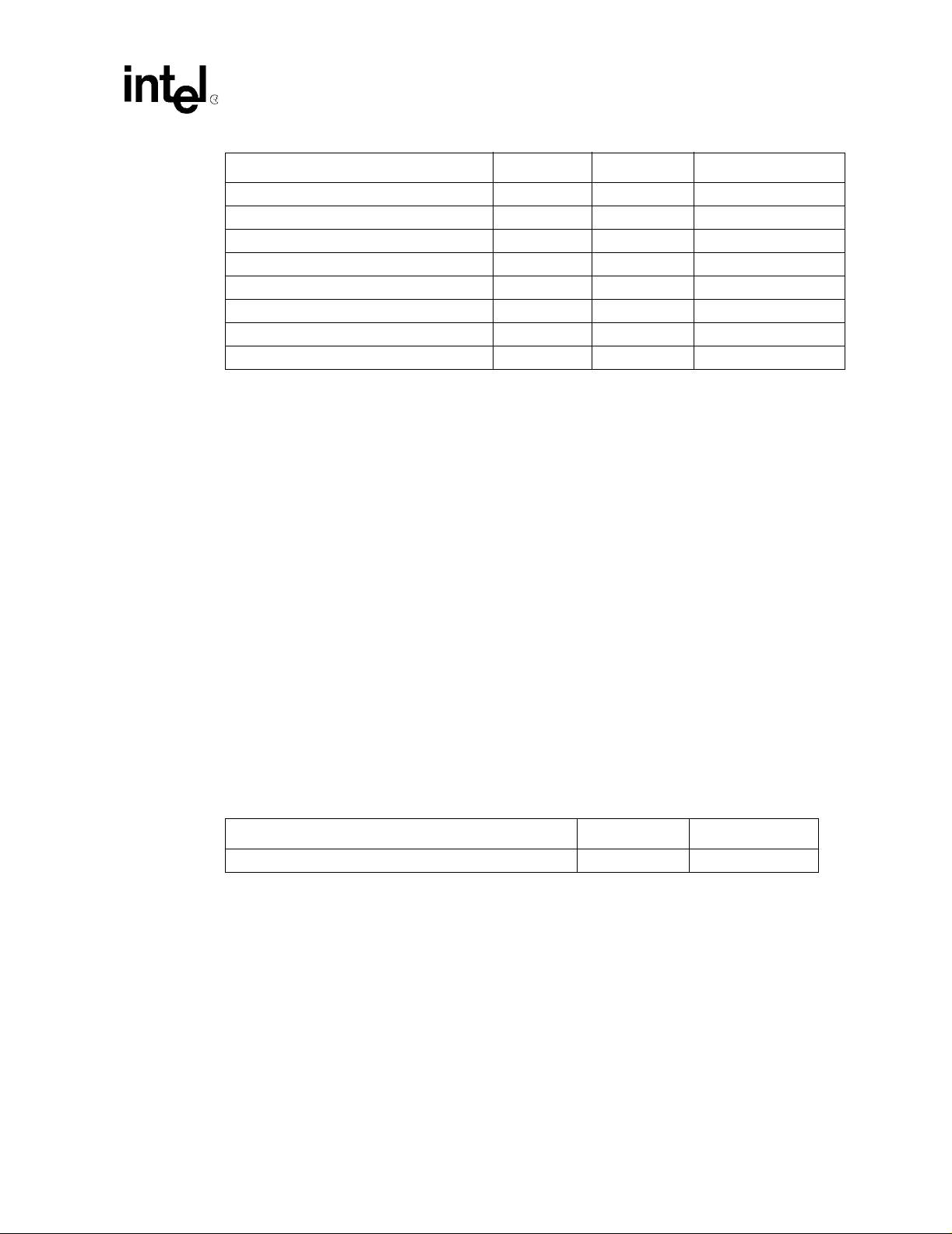
Coprocessors
Function OPC_2 CRm Data
Load Buffer 2 with one word 0b010 0b0010 Virtual address
Load Buffer 2 with four words 0b010 0b0110 Virtual address
Load Buffer 2 with eight words 0b010 0b1010 Virtual address
Load Buffer 3 with one word 0b010 0b0011 Virtual address
Load Buffer 3 with four words 0b010 0b0111 Virtual address
Load Buffer 3 with eight words 0b010 0b1011 Virtual address
Disable user-mode MCR access 0b100 0b0000 Ignored
Enable user-mode MCR access 0b101 0b0000 Ignored
See Chapter 5, “Caches, Write Buffer, and Read Buffer” for details on the use and operation of the
read buffer.
Note: The write buffer must be flushed prior to loading the read buffer to maintain coherency between the
two buffers. But, if user-mode MCR access is enabled for the read buffer and the flush is attempted
while in user mode, an undefined instruction exception will occur. In this case, the exception
handler must perform the write buffer flush, then return to user mode to execute the read buffer
load. Alternatively, an SWI instruction can be used as a service call to flush the write buffer.
6.2.11 Registers 10 – 12 RESERVED
Accessing registers 10 – 12 may yield unpredictable results.
6.2.12 Register 13 – Process ID Virtual Address Mapping
The SA-1110supports the remapping of virtual addresses through a process ID (PID) register. The
6-bit PID value is OR’ed with bits 30..25 of the virtual address when bits 31..25 of the virtual
address are zero. This effectively remaps the address to one of 64 “slots” in the lower 2 Gbyte
address space. The following table shows the OPC_2 and CRm field encodings used t o access the
process ID register.This register is zero at reset and if left unmodified, effectively disables the
remapping function. As such, no explicit enable or disable f unction is necessary. Reserved bits read
as zero and must be written as zero. This register is readable and writable.
Function OP C_2 CRm
Access process ID register 0b000 0b0000
The following figure shows the format of the process ID register.
SA-1110 Developer’s Manual 61
Page 62

Coprocessors
31 30 29 28 27 26 25 24 23 22 21 20 19 18 17 16 15 14 13 12 11 10 9 8 7 6 5 4 3 2 1 0
Register 13 – Process ID Read/Write
Process ID
Reserved
Reserved
6.2.13 Register 14 – Debug Support (Breakpoints)
The SA-1110 supports address and data breakpoints through register 14 of coprocessor 15. The
instruction formats follow. For a description of the breakpoint operation, see Chapter 15, “Debug
Support”. The following table shows the OPC_2 and CRm field encodings used to access the
address and data breakpoints.
The DBAR, DBVR, DBMR and DBCR registers are Read/Write registers. The IBCR is a
Write-Only register.
Function OPC_2 CRm
Access data breakpoint address register (DBAR). 0b000 0b0000
Access data breakpoint value register (DBVR). 0b000 0b0001
Access data breakpoint mask register (DBMR). 0b000 0b0010
Load data breakpoint control register (DBCR). 0b000 0b0011
Write instruction breakpoint address and control register (IBCR). 0b000 0b1000
The DBCR register is a 3-bit register used to control the enabling and disabling of the data
breakpoints. Bits 0..2 are valid and positioned as shown below. Bits 3..31 are reserved. These bits
read as zeros and writes have no effect.
Data Breakpoint Control Register
31 30 29 28 27 26 25 24 23 22 21 20 19 18 17 16 15 14 13 12 11 10 9 8 7 6 5 4 3 2 1 0
Bits Name Description
Load watch
0lw
0 – Disable load watch
1 – Enable load watch
(DBCR)
Reserved
62 SA-1110 Developer’s Manual
Read/Write
saw
sdw
lw
Page 63

Coprocessors
Data Breakpoint Control Register
31 30 29 28 27 26 25 24 23 22 21 20 19 18 17 16 15 14 13 12 11 10 9 8 7 6 5 4 3 2 1 0
Bits Name Description
Store address watch
1saw
2sdw
31..3 — Reser ved.
0 – Disable store address watch
1 – Enable store address watch
Store data watch
0 – Disable store data watch
1 – Enable store data watch
(DBCR)
Reserved
Read/Write
saw
sdw
The IBCR is a write-only register used to load an address breakpoint address and to set an enable
bit for the function. If an address is loaded with bit 0 (E) set, then the address is enabled as a
breakpoint. If bit zero is cleared, then the breakpoint is disabled. Bit 1 is reserved and should be
written to zero.
Instruction Breakpoint Address
and Control Register (IBCR)
Write-Only
lw
31 30 29 28 27 26 25 24 23 22 21 20 19 18 17 16 15 14 13 12 11 10 9 8 7 6 5 4 3 2 1 0
Instruction Address Breakpoint Value
Bits Name Description
Address break enable/disable.
0E
1 —
31..2 Address breakpoint address.
0 – Disable
1 – Enable
Reserved.
Should be written as zero.
6.2.14 Register 15 – Test, Clock, and Idle Control
Register 15 is a write-only register. The CRm and OPC_2 fields are used to encode the following
control operations. Operation for all other values of OPC_2 and CRm is unpredictable.
E
Reserved
SA-1110 Developer’s Manual 63
Page 64

Coprocessors
Function OPC_2 CRm
Enable odd-word loading of the linear feedback shift
register ( LFSR)
Enable even-word loading of LFSR 0b001 0b0010
Clear LFSR 0b001 0b0100
Move LFSR to R14.abort 0b001 0b1000
Enable clock switching 0b010 0b0001
Disable clock switching 0b010 0b0010
RESERVED 0b010 0b0100
Wait for interrupt 0b010 0b1000
0b001 0b0001
64 SA-1110 Developer’s Manual
Page 65

Memory Management Unit (MMU) 7
This chapter describes the memory management functions.
7.1 Overview
The Intel®StrongARM*SA-1110 Microprocessor (SA-1110) implements the standard ARM
memory-management functions using two 32-entry fully associative translation buffers (TBs). One
is used for instruction accesses and the other for data accesses. On a TB miss, the translation table
hardware is invoked to retrieve the translation and access permission information. Once retrieved,
if the entry maps to a valid page or section, then the information is placed into the TB. The
replacement algorithm in the TB is round robin. For an invalid page or section, an abort is
generated and the entry is not placed in the TB.
7.1.1 MMU Registers
See Section 6.2, “Coprocessor 15 Definition” on page 6-56 foradescriptionoftheMemory
Management Unit (MMU) coprocessor 15 registers supported by the SA-1110.
7.2 MMU Faults and CPU Aborts
The MMU generates four faults:
• Alignment fault
• Translation fault
• Domain fault
• Permission fault
*
Alignment faults are generated by word l oads or stores with the low-order two address bits
nonzero, and by load or store half words when the low-order address bit is a one. Translation faults
are generated by access to pages marked invalid by the memory-management page tables. Domain
faults and permission faults are generated by accesses to memory that are protected by the current
mode, domain, and page protection. See the ARM Architecture Reference for more information. In
addition, an external abort may be raised on external data accesses.
7.3 Data Aborts
The SA-1110 takes a data abort exception due to: MMU-generated exceptions, accessing reserved
memory space.
SA-1110 Developer’s Manual 65
Page 66

Memory Management Unit (MMU)
7.3.1 Cacheable Reads (Linefetches)
A linefetch can be safely aborted on any word in the transfer. If an abort occurs during the
linefetch, the cache is purged so it will not contain invalid data. If the abort happens before the
word that was requested by the access is returned, the load is aborted. If the abort happens after the
word that was requested by the access is returned, the load completes and the fill is aborted (but no
exception is generated).
7.3.2 Buffered Writes
Buffered writes cannot be externally aborted. Therefore, the system should be configured such that it
does not perform buffered writes to areas of memory that are capable of flagging an external abort.
7.4 Interaction of the MMU, Icache, Dcache, and Write Buffer
The MMU, Icache, Dcache, and WB can be enabled or disabled independently. The Icache can be
enabled with the MMU enabled or disabled. However, the Dcache and WB can only be enabled
when the MMU is enabled. Because the write buffer is used to hold dirty copy-back cached lines
from the Dcache, it must be enabled along with the Dcache. Therefore, only four of the eight
combinations of the MMU, Dcache, and WB enables are valid. There are no hardware interlocks
on these restrictions, so invalid combinations will cause undefined results.
Table 7-1. Valid MMU, Dcache, and Write Buffer Combinations
MMU Dcache Write Buffer
Off Off Off
On Off Off
On Off On
On On On
The following procedures must be observed.
To enable the MMU:
1. Program the translation table base and domain access control registers.
2. P r ogram level 1 and level 2 page tables as required.
3. Enable the MMU by setting bit 0 in the control register.
66 SA-1110 Developer’s Manual
Page 67

Memory Management Unit (MMU)
Note: Care must be taken if the translated address differs from the untranslated address because the three
instructions following the enabling of the MMU will have been fetched using “flat translation”, and
enabling the MMU may be considered a branch with delayed execution. A similar situation occurs
when the MMU is disabled. Consider the following code sequence:
MOV R1, #0x1
MCR 15,0,R1,0,0 ; Enable MMU
Fetch nontranslated
Fetch nontranslated
Fetch nontranslated
Fetch Translated
To disable the MMU:
1. Disable the WB by clearing bit 3 in the control register.
2. Disable the Dcache by clearing bit 2 in the control register.
3. Disable the Icache by clearing bit 12 in the control register.
4. Disable the MMU by clearing bit 0 in the control register.
Note: If the MMU is disabled and subsequently reenabled, the contents of the TB is preserved. If the
contents are now invalid, the TB should be flushed before reenabling the MMU.
7.5 Mini Data Cache
The mini data cache is a 16-entry, 2-way set-associative data cache. It is accessed in parallel with
the main data cache. A data reference is allocated into the mini data cache if the B and C bits in
the MMU are 0 and 1, respectively. A line of data can reside only in one of the two Dcaches at any
one time. BothDcaches must be flushed prior to any page table manipulation that could change the
allocation policy.
SA-1110 Developer’s Manual 67
Page 68

Page 69

Clocks 8
This section describes the Intel®StrongARM*SA-1110 Microprocessor (SA-1110) clocks. The
following diagram shows the distribution of clocks in the SA-1110. The 3.6864-MHz oscillator
feeds both PLLs. The primary PLL provides clocks for the core logic and a 7.36-MHz clock for
several of the serial controllers. The core, Dcaches, and read and write buffers use either the
full-speed core clock or the divided-down clock. The LCD controller, DMA, memory controller,
and GPIO use the core clock divided by 2 (RCLK). The 32.768-kHz oscillator feeds the real-time
clock (RTC)and the power manager logic. The secondary PLL provides the clock for the UDC, the
ICP, and the MCP. The oscillators and PLLs are completely integrated with the SA-1110 and
require no external devices other than the crystals for operation.The following figure shows a block
diagram of the clocking system for the SA-1110.
Figure 8-1. SA-1110 Clock System Block Diagram
Intel® ARM*
SA-1 Core
Divide
32.768 kHz
Oscillator
3.6864 MHz
Oscillator
by 2
Primary PLL
59 MHz - 200 MHz
I-Cache
D-Cache
Write Buffer
Read Buffer
Memory
Controller
GPIO 27
Secondary PLL
48 MHz
RTC and Power
Manager
Peripherals
UART: 7.36 MHz
ICP: 7.36 or 48 MHz
MCP/SSP: 7.36 or 12 MHz
PPC: 7.36 MHz
UDC: 48 MHz
LCD
Controller
DMA
Controller
8.1 Intel®StrongARM SA-1110 Crystal Oscillators
The SA-1110 clocks are derived from two crystals connected to on–chip oscillators. The first clock
source is a 3.6864-MHz crystal that feeds the CPU PLL and the 48-MHz PLL. The CPU PLL
multiplies the oscillator output up to the core frequency. This frequency is then divided down to
generate baud rates for the serial ports. If the UARTs are not being used or do not need standard
I/O
Controller
A8054-01
SA-1110 Developer’s Manual 69
Page 70

Clocks
baud rates, then the 3.6864 -Hz oscillator may be replaced with a 3.5795-MHz crystal to generate
frequencies as shown in Table 8-1.The second oscillator is connected to a 32.768-kHz crystal. The
output of this oscillator clocks the power management controller and the real-time clock (RTC).
See Appendix B, “3.6864–MHz Oscillator Specifications” and Appendix C, “32.768–KHz
Oscillator Specifications” for detailed specifications of the crystal oscillators.
8.2 Core Clock Configuration Register
The core clock frequency is configured by software through the core cl ock configuration field
(CCF[4:0]) in the power manager phase-locked loop (PLL) configuration register (PPCR). This
field should be programmed during the boot sequence for the desired full-speed operation.
nRESET clears the field by selecting the lowest frequency operation.
See Section 9.5, “Power Manager” on page 9-99 for the physical address used to access this
register.
Table 8-1 shows the core clock frequency as a function of the CCF setting.
Table 8-1. Core Clock Configura tions
CCF[4:0] Core Clock F requency in MHz
3.6864-MHz Crystal Oscillator 3.5795-MHz Crystal Oscillator
00000 59.0 57.3
00001 73.7 71.6
00010 88.5 85.9
00011 103.2 100.2
00100 118.0 114.5
00101 132.7 128.9
00110 147.5 143.2
00111 162.2 157.5
01000 176.9 171.8
01001 191.7 186.1
01010 206.4 200.5
01011 221.2 214.8
01100– 11111 Not supported. —
The actual core clock (DCLK) can switch between being driven by the high speed core clock
(CCLK, set by CCF[4:0]) and the memory clock (MCLK), which runs at half the frequency of
CCLK. CCLK is used except when the SA-1110 is wait ing for fills to complete after a cache miss.
At reset, clock switching is disabled and the DCLK is driven by MCLK. Clock switching can also
be disabled by writing to CP15 register 15 with OPC_2 = 2 and CRm = 2 (see Section 6.2.14).
Clock switching is enabled by writing to CP15 register 15 with OPC_2 = 2 and CRm = 1.
Disabling clock switching only disables switching for DCLK; it does not force the DCLK to
MCLK. However, DCLK can be forced to MCLK by forcing an instruction or data cache miss after
clock switching is disabled.
70 SA-1110 Developer’s Manual
Page 71

Clocks
8.2.1 Restrictions on Changing the Core Clock Configuration
When the CPU writes to the PPCR, the core clock PLL and the 48-MHz PLL are stopped for a
period of time to allow the core clock PLL to relock to the new frequency. When these PLLs are
stopped, the core clock and all clocks derived from that clock are stopped. When this happens,
certain units within the SA-1110 (the LCD controller, all serial controllers, the DMA controller,
and the OS timer) will experience an interruption in operation for approximately 150 microseconds
after the PPCR is written.
Because of these restrictions, it is recommended that the user not change the PPCR except
immediately following a hard reset or immediately following wake-up from sleep mode. The LCD
controller, all ser ial controllers (except the UDC), the DMA controller, and the OS timer are
already disabled and are not affected by an interruption in their clock stream. In addition to these
restrictions, the PPCR must be written prior to enabling clock switching. Note that the 32.768-kHz
clock is not affected by any change in the PPCR and units using this clock (power management,
RTC) do not see any interruption in service during the 150 microsecond period.
8.3 DrivingIntel®StrongARM SA-1110 Crystal Pins from an External Source
In most applications, a 3.6864-MHz crystal will be connected between the PXTAL and the
PEXTAL pins. Similarly, a 32.768-kHz crystal will be connected between the TXTAL and
TEXTAL pins. In some applications, supplying these clocks from an external source may be
preferred. This is accommodated in the SA-1110 design by:
• Supplying the 32.768-kHz clock from an external source
— Only the TXTAL pin is driven. The TEXTAL pin must be left floating.
— The peak-to-peak voltage swing on TXTAL must be at least 0.6 V and the voltage on the
pin must remain within the range of 0 V to 1 V, independent of the other power supply
voltages applied to the processor.
• Supplying a 3.6864-MHz clock from an external source
— Both PXTAL and PEXTAL are driven with complementary signals.
— The peak-to-peak voltage swing on PXTAL and PEXTAL must be at least 0.6 V and the
voltage on the pin must remain in the range of 0 V to 1 V, independent of the other power
supply voltages applied to the processor.
— When an external clock is being used, the pull-down path in the i nternal 3.6864 MHz
oscillator is active. To limit the current into the internal oscillator, it is recommended that
the minimum impedance to the positive supply be controlled. The maximum current
sourced by the external clock source when the clock is at its maximum positive voltage
should be about 1 mA.
— The maximum impedance of the external clock source is set by the minimum slew rate at
the PXTAL and PEXTAL pins, approximately 1 V per 100 ns.
†
These constraints can be satisfied by the following suggestions:
†
†
†
• For applications in which a pulse generator is available, drive differential 1-V signals through
series 1-K resistors (after the usual 50-ohm terminators-to-ground).
SA-1110 Developer’s Manual 71
Page 72

Clocks
• To supply external clock s ignals from a 3.3-V supply, drive signals with open collector or
tristateable drivers. Set high lev el with 3.3 K from 3.3 V to the output and 1.3 K from the
output to ground.
• To supply external clock s ignals from a 1.5-V supply, drive signals with open collector or
tristatable drivers. Set high level with 1.5 K from 1.5 V to the output and 2.7 K from output to
ground. This solution may be preferred in portable applications that turn off the 1.5-V supply
in sleep mode because this would eliminate the current through the resistors in sleep mode.
The two pairs of crystal pins are located close to each other on the processor. This arrangement is
advantageous when there are crystals connected to the pins because the low signal swings and slow
edges result in limited noise coupling between the pins. If one of the crystals is replaced by an
independent signal source and the other is not, some degradation of the remaining crystal oscillator
performance can result due to increased noise coupling. If only one crystal is being used, this effect
can be reduced by limiting the speed of the edge rate on the pin driven by the independent source.
If the PXTAL or TXTAL pin is driven above the voltage indicated, there will be no permanent
damage to the processor for pin voltages less than 2.5 V. However, ESD diodes on these pins will
attempt to clamp the voltage at approximately 1.5 V. The clamping action results in significant
noise injected into an internally generated supply used by several sensitive circuits on the
processor. Consequently, driving this pin higher than the 1 V limit can result i n unpredictable
operation not obviously connected with the crystal pins. It is advised to not drive the crystal pins
higher than 1 V even if there is no obvious side effect.
Note: In every system, there must be a provision for both a 3.6864-MHz and a 32.768-kHz source either
from an external oscillator or a crystal.
8.4 Clocking During Test
If TCK_BYP is high, then the PLLs and oscillators are not used and the high-speed core clock is
supplied externally on the TESTCLK pin. This mode is for testing only and is not supported for
standard operation.
72 SA-1110 Developer’s Manual
Page 73

System Control Module 9
This chapter describes the system control module that controls several processor-wide system
functions. The units contained in the system control module are: the general-purpose I/O ports, the
interrupt controller, the real-time clock, the operating system timer, the power manager, and the
reset controller.
9.1 General-Purpose I/O
The Intel®StrongARM*SA-1110 Microprocessor (SA-1110) provides 28 general-purpose I/O
(GPIO) port pins for use in generating and capturing application-specific input and output signals.
Each pin is programmable as an input or output and as an interrupt source. All 28 pins are
configured as inputs during the assertion of reset, and remain inputs until they are configured
otherwise.
Each GPIO pin can be configured as an input or an output by programming the GPIO pin direction
register (GPDR). When programmed as an output, the pin can be controlled by writing to the GPIO
pin output set register (GPSR) and the GPIO pin output clear register (GPCR). Writing to these
registers controls the output data register, which is not directly readable or writable. The set and
clear registers can be written regardless of whether the pin is configured as an input or an output.
The programmed o utput state will take effect when the pin is reconfigured as an output.
When programmed as an input, the current state of each GPIO pin can be read through the GPIO
pin-level register (GPLR). This regist er can be read at any time and can be used to confirm the state
of the pin when it is configured as an output. In addition, each GPIO pin can be programmed to
detect a rising and/or falling edge through the GPIO rising-edge detect register (GRER) and GPIO
falling-edge detect register (GFER). The state of the edge detect can be read through the GPIO
edge detect status register (GEDR). These edge detects can be programmed to generate an interrupt
(see the Section 9.2, “Interrupt Controller” on page 9-83) or to serve as a wake-up event to bring
the SA-1110 out of sleep mode (see the Section 9.5, “Power Manager” on page 9-99).
When the SA-1110 enters sleep mode, the contents of the power manager sleep state register
(PGSR) is loaded into the output data register. If the particular pin is programmed as an output,
then the state in the PGSR will be driven onto the pin b efore entering sleep. When the SA-1110
exits sleep mode, these values remain until reprogrammed by writing to the GPSR and GPCR.
Some GPIO pins can also serve an alternate function within the SA-1110. Certain modes within the
serial controllers and LCD controller require extra pins. These functions are hard–wired into
specific GPIO pins. How these functions are used is described in the following sections. Even
though a GPIO pin has been taken over for an alternate function, you must still p rogram the correct
direction of that pin through the GPDR. Details on alternate functions are also provided in
following sections. Figure 9-1 shows a block diagram of a single GPIO pin.
SA-1110 Developer’s Manual 73
Page 74
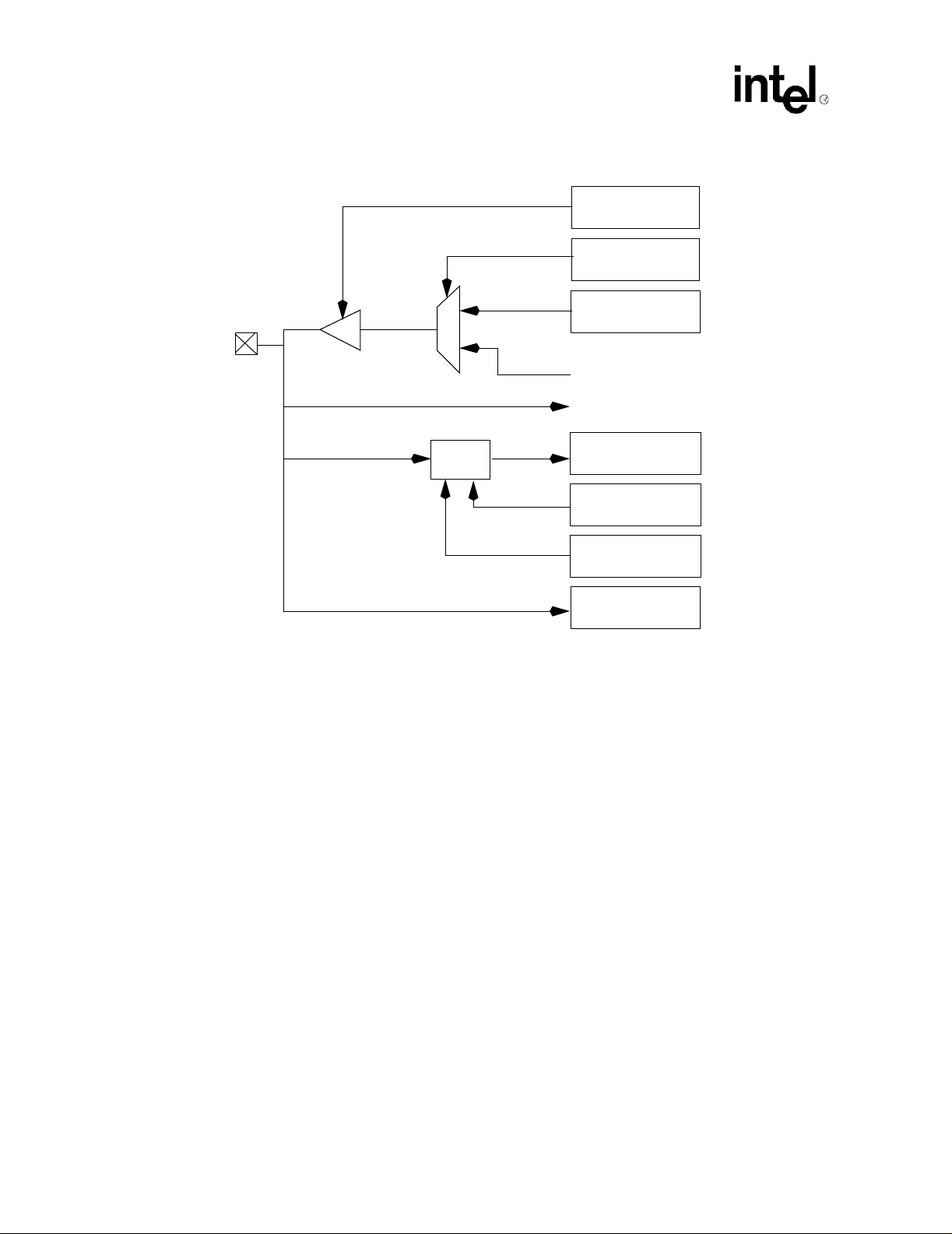
System Control Module
Figure 9 -1. General-Purpose I/O Block Diagram
Pin Direction
Register
Alternate Function
Register
0
GPIO Pin
1
Edge
Detect
9.1.1 GPIO Register Definitions
There are a total of eight registers within the GPIO control block: one is used to monitor pin state;
two are used to control pin state; one is used to control pin d irection; two are used to specify a pin’s
edge type that should be detected; and one is used to flag when specified edge types are detected on
pins.
Pin Set and
Clear Registers
Alternate Function
(Output)
Alternate Function
(Input)
Edge Detect
Status Register
Rising Edge Detect
Enable Register
Falling Edge Detect
Enable Register
Pin-Level
Register
The last register indicates whether a pin is used as normal GPIO or whether it is taken over by the
alternate function. The values in all other GPIO registers are unknown following reset and must be
initialized by software.
Note: A question mark (?) signifies that the Reset value of that bit is undefined when the processor has
completed its reset cycle.
74 SA-1110 Developer’s Manual
Page 75

9.1.1.1 GPIO Pin-Level Register (GPLR)
The state of each of the GPIO port pins is visible through the GPIO pin-level register (GPLR).
Each bit number corresponds to the port pin number from bit 0 to bit 27. This is a read-only register
that is used to determine the current level of a particular pin (regardless of the programmed pin
direction).
The following table shows the locations of the 28 pin-level bits within the GPLR. This is a
read-only register.For reserved bits, reads return zero; a question mark indicates that the values are
unknown at reset.
.
0h 9004 0000 GPLR Read-Only
31 30 29 28 27 26 25 24 23 22 21 20 19 18 17 16 15 14 13 12 11 10 9 8 7 6 5 4 3 2 1 0
System Control Module
Reserved
Reset 0 0 0 0 ? ? ? ? ? ? ? ? ? ? ? ? ? ? ? ? ? ? ? ? ? ? ? ? ? ? ? ?
Bits Name Description
nPLn
31..28 — Reserved
PL27
PL26
PL25
PL24
PL23
PL22
PL21
PL20
PL19
PL18
PL17
PL16
PL15
PL14
PL13
PL12
GPIO port pin level n (where n = 0 through 27).
0 – Pin state is low.
1 – Pin state is high
PL9
PL8
PL7
PL6
PL5
PL4
PL3
PL2
PL11
PL10
PL1
Note: A question mark (?) signifies that the Reset value of that bit is undefined when the processor has
completed its reset cycle.
PL0
SA-1110 Developer’s Manual 75
Page 76

System Control Module
9.1.1.2 GPIO Pin Direction Register (GPDR)
Pin direction is controlled by programming the GPIO pin direction register (GPDR). The GPDR
contains one direction control bit for each of the 28 port pins. If a direction bit is programmed to a
one, the port is an output. If it is programmed to a zero, it is an input. At hardware reset, all bits in
this register are cleared, configuring all GPIO pins as inputs. Soft resets and sleep reset have no
effect on this register. For reserved bits, writes are ignored and reads return zero. The following
table shows the location of each pin direction bit in the GPIO pin direction register.
.
0h 9004 0004 GPDR Read/Write
31 30 29 28 27 26 25 24 23 22 21 20 19 18 17 16 15 14 13 12 11 10 9 8 7 6 5 4 3 2 1 0
Reserved
Reset 0 0 0 0 0 0 0 0 0 0 0 0 0 0 0 0 0 0 0 0 0 0 0 0 0 0 0 0 0 0 0 0
Bits Name Description
nPDn
31..28 — Reserved
PD27
PD26
PD25
PD24
PD23
PD22
PD21
PD20
PD19
PD18
PD17
PD16
PD15
PD14
GPIO port pin direction n (where n = 0 through 27).
0 – Pin configured as an input.
1 – Pin configured as an output.
PD13
PD12
PD9
PD8
PD7
PD6
PD5
PD4
PD3
PD2
PD11
PD10
PD1
PD0
76 SA-1110 Developer’s Manual
Page 77
System Control Module
9.1.1.3 GPIO Pin Output Set Register (GPSR) and Pin Output Clear Register (GPCR)
When a port is configured as an output, the user controls the state of the pin by writing to either the
GPIO pin output set register (GPSR) or the GPIO pin output clear register (GPCR). An output pin
is set by writing a one to its corresponding bit within the GPSR. To clear an output pin, a one is
written to the corresponding bit within the GPCR. These are write-only registers. Reads return
unpredictable values. Writing a zero to any of the GPSR or GPCR bits has no effect. Writing a one
to a GPSR or GPCR bit corresponding to a pin that is configured as an input has no effect. For
reserved bits, writes are ignored. The following tables show the locations of the GPSR bits and the
locations of the GPCR bits. These are write-only registers and reset values do not apply.
0h 9004 0008 GPSR Write-O nly
31 30 29 28 27 26 25 24 23 22 21 20 19 18 17 16 15 14 13 12 11 10 9 8 7 6 5 4 3 2 1 0
Reserved
Reset ? ? ? ? ? ? ? ? ? ? ? ? ? ? ? ? ? ? ? ? ? ? ? ? ? ? ? ? ? ? ? ?
Bits Name Description
nPSn
31..28 — Reserved
31 30 29 28 27 26 25 24 23 22 21 20 19 18 17 16 15 14 13 12 11 10 9 8 7 6 5 4 3 2 1 0
Reserved
Reset ? ? ? ? ? ? ? ? ? ? ? ? ? ? ? ? ? ? ? ? ? ? ? ? ? ? ? ? ? ? ? ?
Bits Name Description
nPCn
31..28 — Reserved
PS27
PS26
PS25
PS24
PS23
PS22
PS21
PS20
PS19
PS18
PS17
PS16
PS15
PS14
PS13
PS12
GPIO output pin set n (where n = 0 through 27).
0 – Pin level unaffected.
1 – If pin conf igured as an output, set pin level high (one).
0h 9004 000C GPCR Write-Only
PC27
PC26
PC25
PC24
PC23
PC22
PC21
PC20
PC19
PC18
PC17
PC16
PC15
PC14
PC13
PC12
GPIO output pin clear n (where n = 0 through 27).
0 – Pin level unaffected.
1 – If pin conf igured as an output, clear pin level low (zero).
PS9
PS8
PS7
PS6
PS5
PS4
PS3
PS2
PS11
PS10
PC9
PC8
PC7
PC6
PC5
PC11
PC10
PC4
PS1
PC3
PC2
PC1
PS0
PC0
The user can test a bit within the GPLR corresponding to a pin that is configured as an output after
having set or cleared the pin state to determine if there is an external conflict on the pin. For
example, if an off-chip device is driving a GPIO output pin high and the user has cleared the pin’s
state by writing a one to its GPCR bit, the user can read the GPLR, then compare the written value
(zero) to the actual value (one) to detect the conflict.
SA-1110 Developer’s Manual 77
Page 78

System Control Module
9.1.1.4 GPIO Rising-Edge Detect Register (GRER) and Falling-Edge Detect Register (GFER)
Each GPIO port can also be programmed to detect a rising-edge, falling-edge, or either transition
on a pin. When an edge is detected that matches the type of edge programmed for the pin, a status
bit is set. The interrupt controller can be programmed to signal an interrupt to the CPU or wake up
the SA-1110 from sleep mode when any one of these status bits is set.
The GPIO rising-edge and falling-edge detect registers (GRER and GFER, respectively) are used
to select the type of transition on a GPIO pin that causes a bit within the GPIO edge detect status
register (GEDR) to be set. For a given GPIO port pin, its corresponding GRER bit is set to cause a
GEDR status bit to be set when the pin transitions from logic level zero (0) to one (1). Likewise,
GFER is used to set the corresponding GEDR status bit when a transition from logic level one (1)
to zero (0) occurs. When the corresponding bits are set in both registers, either a falling- or a
rising-edge transition causes the corresponding GEDR status bit to be set.
The following table shows both the rising-edge and falling-edge enable bit locations corresponding
to all 28 port pins. For reserved bits, writes are ignored and reads return zero; a question mark
indicates that the values are unknown at reset.
0h 9004 0010 GRER Read/Write
31 30 29 28 27 26 25 24 23 22 21 20 19 18 17 16 15 14 13 12 11 10 9 8 7 6 5 4 3 2 1 0
Reserved
Reset 0 0 0 0 ? ? ? ? ? ? ? ? ? ? ? ? ? ? ? ? ? ? ? ? ? ? ? ? ? ? 1 1
Bits Name Description
nREn
31..28 — Reserved
31 30 29 28 27 26 25 24 23 22 21 20 19 18 17 16 15 14 13 12 11 10 9 8 7 6 5 4 3 2 1 0
Reserved
Reset 0 0 0 0 ? ? ? ? ? ? ? ? ? ? ? ? ? ? ? ? ? ? ? ? ? ? ? ? ? ? 1 1
Bits Name Description
nFEn
31..28 — Reserved
RE27
RE26
RE25
RE24
RE23
RE22
RE21
RE20
RE19
RE18
RE17
RE16
RE15
RE14
RE13
RE12
GPIO pin n rising-edge det ect (where n = 0 through 27).
0 – Disable rising-edge detect.
1 – Set corresponding GEDR status bit when a rising edge is detected on the GPIO pin.
0h 9004 0014 GFER Read/Write
FE27
FE26
FE25
FE24
FE23
FE22
FE21
FE20
FE19
FE18
FE17
FE16
FE15
FE14
FE13
FE12
GPIO pin n falling-edge det ect (where n = 0 through 27).
0 – Disable falling-edge detect.
1 – Set corresponding GEDR status bit when a falling edge is detected on the GPIO pin.
RE9
RE8
RE7
RE6
RE5
RE4
RE3
RE2
RE11
RE10
FE9
FE8
FE7
FE6
FE5
FE11
FE10
FE4
RE1
FE3
FE2
FE1
RE0
FE0
78 SA-1110 Developer’s Manual
Page 79
9.1.1.5 GPIO Edge Detect Status Register (GEDR)
The GPIO edge detect status register (GEDR) contains 28 status bits that correspond to the 28
GPIO port pins. When an edge detect occurs on a pin that matches the type of edge programmed in
the GRER and/or GFER registers, the corresponding status bit is set in GEDR. Once a GEDR bit is
set, the CPU must clear it. GEDR status bits are cleared by writing a one to them. Writing a zero to
a GEDR status bit has no effect.
Each edge detect that sets the corresponding GEDR status bit for GPIO pins 0 – 27 can trigger an
interrupt request. Pins 27 – 11 together form a group that can cause one interrupt request to be
triggered when any one of the GEDR status bits 27 – 11 is set. Each of GPIO pins 10 – 0 causes an
independent first-level interrupt. See the Section 9.2, “ Interrupt Controller” on page 9-83 for a
description of the programming of GPIO interrupts. The following table shows a summary of
GEDR; a question mark indicates that the values are unknown at reset.
0h 9004 0018 GEDR Read/Write
31 30 29 28 27 26 25 24 23 22 21 20 19 18 17 16 15 14 13 12 11 10 9 8 7 6 5 4 3 2 1 0
System Control Module
Reserved
Reset 0 0 0 0 ? ? ? ? ? ? ? ? ? ? ? ? ? ? ? ? ? ? ? ? ? ? ? ? ? ? ? ?
Bits Name Description
nEDn
31..28 — Reserved
ED27
ED26
ED25
ED24
ED23
ED22
ED21
ED20
ED19
ED18
ED17
ED16
ED15
ED14
ED13
ED12
GPIO edge detect status n (where n = 0 t hrough 27).
0 – No edge detect has occurred on pin as specified in GRER and/or GFER.
1 – Edge detect has occurred on pin as specified in GRER and/or GFER.
ED9
ED8
ED7
ED6
ED5
ED4
ED3
ED2
ED11
ED10
ED1
ED0
SA-1110 Developer’s Manual 79
Page 80

System Control Module
9.1.1.6 GPIO Alternate Function Register (GAFR)
The GPIO alternate function register (GAFR) contains 28 control bits that correspond to the 28
GPIO port pins. When the processor sets a bit in the GAFR, the corresponding GPIO pin is
switched over to that pin’s alternate function. See the following section for details on alternate
functions. This register is cleared to all zeros on all reset conditions.
0h 9004 001C GAFR Read/Write
31 30 29 28 27 26 25 24 23 22 21 20 19 18 17 16 15 14 13 12 11 10 9 8 7 6 5 4 3 2 1 0
Reserved
Reset 0 0 0 0 0 0 0 0 0 0 0 0 0 0 0 0 0 0 0 0 0 0 0 0 0 0 0 0 0 0 0 0
Bits Name Description
nAFn
31..28 — Reserved
AF27
AF26
AF25
AF24
AF23
AF22
AF21
AF20
AF19
AF18
AF17
AF16
AF15
AF14
AF13
AF12
GPIO alternate function bits (where n = 0 through 27).
A bit set in this register indicates that the corresponding GPIO pin is to be used for its
alternate function. A zero in this register indicates that the corresponding GPIO pin is to be
used for its normal GPIO function.
AF9
AF8
AF7
AF6
AF5
AF4
AF3
AF2
AF11
AF10
AF1
AF0
80 SA-1110 Developer’s Manual
Page 81

9.1.2 GPIO Alternate Fun ctions
Most GPIO pins have an alternate function that can be invoked to enable additional functionality
within the SA-1110. If a GPIO is used for this alternate function, then it cannot be used as a GPIO
at the same time. Pins 0 and 1 are reserved because of their special use during sleep mode and are
not available for any alternate function. The following table shows each GPIO pin and its
corresponding al ternate function. For more details on an alternate function, see the section that
corresponds to its name in the Unit column in the table.
Pin Alternate Function Direction Unit Signal Description
GP 27 32KHZ_OUT
GP 26 RCLK_OUT
GP 25 RTC clock
GP 24 Reserved
GP 23 TREQB
GP 22 TREQA
GP 21 TIC_ACK
GP 21 MCP_CLK
GP 20 UART_SCLK3
GP 19 SSP_CLK
GP 18 UART_SCLK1
GP 17 Reserved
GP 16 GPCLK_OUT
GP 15 UART_RXD
GP 14 UART_TXD
GP 13 SSP_SFRM
GP 12 SSP_SCLK
GP 11 SSP_RXD
GP 10 SSP_TXD
GP 2..9 LDD 8..15
GP 1 Reserved
GP 0 Reserved
†
†
†
/MBREQ Input Test controller Either TIC request A or MBREQ
†
/MBGNT Output Test controller
Output Clocks Raw 32.768-kHz oscillator output
Output Clocks Internal clock/2
Output RTC Real time clock
— — —
Input Test controller TIC request B
Input Serial port 4 M CP clock in
Input Serial port 3:UART Sample clock input
Input Serial port 4:SSP Sample clock input
Input Serial port 1:UART Sample clock input
— — —
Output Serial port 1 General-purpose clock out
Input Serial port 1:UART UART receive
Output Serial port 1:UART UART transmit
Output Serial Port 4:SSP S SP frame clock
Output Serial port 4:SSP SSP se rial clock
Input Serial port 4:SSP SSP receive
Output Serial port 4:SSP SSP transmit
Output LCD controller
— — No alternate function
—- — No alternate function
System Control Module
EitherTIC acknowledge or
MBGNT
High-order data pins for
split-screen color LCD support
† Toenable RCLK_OUT, it is also necessary to set bits [31:29] of the Test Unit Control Register (TUCR) =
0b100. See Appendix D, “Internal Test”for more information a bout the TUCR.
† The signals, TREQA, TREQB, and TIC_ACK are reserved by Intel for test purposes.
SA-1110 Developer’s Manual 81
Page 82

System Control Module
9.1.2.1 3.6864 MHz Option for GP 27 Alternate Output Function
When GP 27 is configured for its alternate output function by setting bit 27 in both the GAFR and
GPDR, b it 29 of the test unit control register (TUCR) at physical address 0x9003 0008 can be set to
select the 3.6864 MHz oscillator output instead of the 32.768 KHz oscillator output. When
TUCR 29 is cleared the 32.768 KHz oscillator output is selected again. Neither option provides a
fixed phase relationship with any other pin signals; and some glitching may occur when switching
between the two options.
The 3.6864 MHz option is particularly useful for companion chips that require some clock cycles
after assertion of VDD_FAULT or BATT_FAULT. The oscillato r output will continue through the
first step of the sleep shutdown sequence, which lasts for one cycle of the power manager’s 32.768
KHz clock (~30 microseconds). Thus, at least 112 cycles of 3.6864 MHz oscillation are provided
prior to shutdown. S ee Section 9.5.3 for a detailed description of sleep mode and the sleep
shutdown sequence.
9.1.3 GPIO Register Locations
The following table shows the registers associated with the GPIO block and the physical addresses
used to access them.
Address Name Description
0h 9004 0000 GPLR G PIO pin-level register
0h 9004 0004 GPDR GPIO pin direction register
0h 9004 0008 GPSR GPIO pin output set register
0h 9004 000C GPCR GPIO pin output clear register
0h 9004 0010 GRER GPIO rising-edge detect register
0h 9004 0014 GFER GPIO falling-edge detect register
0h 9004 0018 GEDR GPIO edge detect status register
0h 9004 001C GAFR GPIO alternate f unct ion register
82 SA-1110 Developer’s Manual
Page 83

9.2 Interrupt Controller
The SA-1110 interrupt controller provides masking capability for all interrupt sources and
combines them into their final state, either an FIQ or IRQ processor interrupt. The interrupt
hierarchy of the SA-1110 is a two-level structure.
The first level of the structure, represented by the interrupt controller IRQ pending register (ICIP)
and the interrupt controller FIQ pending register (ICFP) contain the all-enabled and unmasked
interrupt sources. The interrupt controller p ending register (ICPR) shows both IRQ and FIQ
pending interrupts. Interrupts are enabled at their source and unmasked in the interrupt controller
mask register (ICMR). The ICIP contains the interrupts that are programmed to generate an IRQ
interrupt. The ICFP contains all valid interrupts that are programmed to generate an FIQ interrupt.
This routing is programmed via the interrupt controller level register (ICLR).
The second level o f the interrupt structure is represented by registers contained in the source device
(the device generating the first-level interrupt bit). S econd-level interrupt status gives additional
information about the interrupt and is used inside the interrupt service routine. In general, multiple
second-level interrupts are OR’ed to produce a first- level interrupt bit. The enabling of interrupts
is performed inside the source device.
In most cases, the root source of an interrupt can be determined through reading two register
locations: the ICIP or ICFP (depending on which interrupt handler the software is in) to determine
the interrupting device, followed by the status register within that device to find the exact function
needing service. When the SA-1110 is in idle mode (see the Section 9.5, “Power M anager” on
page 9-99), any enabled interrupt causes it to resume operation. The interrupt mask is ignored
during idle mode if the DIM bit in the interrupt controller control register (ICCR) is set to zero (0).
Figure 9-2 shows a block diagram of the interrupt controller.
System Control Module
Figure 9-2. Interrupt Controller Block Diagram
Interrupt Controller
Level Register (ICLR)
Interrupt Controller
Mask Register (ICMR)
Interrupt Source
Bit
Interrupt Controller
Pending Register (ICPR)
Interrupt Controller
IRQ Pending Register (ICIP)
Interrupt Controller
FIQ Pending Register (ICFP)
All Other Qualified
Interrupt Bits
3131
FIQ
Interrupt
to
Processor
IRQ
Interrupt
to
Processor
SA-1110 Developer’s Manual 83
Page 84

System Control Module
9.2.1 Interrupt Controller Register Definitions
The interrupt controller contains four registers: the interrupt controller IRQ pending register
(ICIP), the interrupt controller FIQ pending register (ICFP), the interrupt controller mask register
(ICMR), and the interrupt controller level register (ICLR). Following reset, the FIQ and IRQ
interrupts are disabled within the CPU, and the states of all of the interrupt controller’s registers are
unknown and must be initialized by software before interrupts are enabled within the CPU.
9.2.1.1 Interrupt Controller Pending Register (ICPR)
The ICPR is a 32-bit read-only register that shows all active interrupts in the system. These bits are
not affected by the state of the mask register (ICMR). The following table shows the pending
interrupt source assigned to each bit position in the ICPR. Also included in the table are the source
units for the interrupts and the number of second-level interrupts associated with each. For more
detail on the second-level interrupts, see the section describing that unit.
Bit Position Unit Source Module # of Level 2 Sources Bit Field Description
IP 31
IP 30 1 One Hz clock TIC occurred.
IP 29
IP 28 1 OS timer equals match register 2.
IP 27 1 OS timer equals match register 1.
IP 26 1 OS timer equals match register 0.
IP 25
IP 24 3 Channel 4 service request.
IP 23 3 Channel 3 service request.
IP 22 3 Channel 2 service request.
IP 21 3 Channel 1 service request.
IP 20 3 Channel 0 service request.
IP 19 Serial port 4b 3 SSP service request.
IP 18 Serial port 4a 8 MCP service request.
IP 17 Serial port 3 6 UART service request.
IP 16 Serial port 2 6+6 UART/HSSP service request.
IP 15 Serial port 1b 6 UART service request.
IP 14 Reserved
IP 13 Serial port 0 6 UDC service request.
IP 12 LCD controller 12 LCD controller service request.
System
Peripheral
Real-time clock
Operating system timer
DMA controller
1 RTC equals alarm register.
1 OS timer equals match register 3.
3 Channel 5 service request.
—
Reserved.
84 SA-1110 Developer’s Manual
Page 85

System Control Module
Bit Position Unit Source Module # of Level 2 Sources Bit Field Description
IP 11 System General-purpose I/O 17 “OR” of GPIO edge detects 27-11.
IP10 1 GPIO10edgedetect.
IP 9 1 GPIO 9 edge detect.
IP 8 1 GPIO 8 edge detect.
IP 7 1 GPIO 7 edge detect.
IP 6 1 GPIO 6 edge detect.
IP 5 1 GPIO 5 edge detect.
IP 4 1 GPIO 4 edge detect.
IP 3 1 GPIO 3 edge detect.
IP 2 1 GPIO 2 edge detect.
IP 1 1 GPIO 1 edge detect.
IP 0 1 GPIO 0 edge detect.
Total level 2 interrupt
sources
110
Several units have more than one source per interrupt signal. When an interrupt is signalled from
one of these units, the interrupt handler routine identifies which interrupt was signalled using the
interrupt controller’s flag register (this identifies the unit that made the request, but not the exact
source). The handler then reads the interrupting unit’s status register to identify which source
within the unit signalled the interrupt. For all interrupts that have one corresponding source, the
interrupt handler routine needs to use only the interrupt controller’s registers to identify the exact
cause of the interrupt.
SA-1110 Developer’s Manual 85
Page 86

System Control Module
9.2.1.2 Interrupt Controller IRQ Pending Register (ICIP) and FIQ Pending Register (ICFP)
The ICIP and the ICFP contain one flag per interrupt (32 total) that indicates an interrupt request
has been made by a unit. Inside the interrupt service routine, the ICIP and ICFP are read to
determine the interrupt source. In general, software then reads status registers within the
interrupting device to determine how to service the interrupt.
Bits within the ICPR are read only, and represent the logical OR of status bits for a given interrupt
within the source unit. Once an interrupt has been serviced, the handler clears the pending interrupt
at the source by writing a one to the necessary status bit. Clearing the interrupt status bit at the
source automatically clears the corresponding ICIP and ICFP flag provided there are no other
interrupt status bits set within the source unit.
All interrupt source status bits are cleared by writing a one to them. Writing a zero to an interrupt
status bit has no effect. The following table shows the bit locations corresponding to the 32
separate interrupt pending status flags in the ICIP. The next table shows the bit locations
corresponding to the 32 separate interrupt pending status flags in the ICFP. This is a read-only
register.
0h 9005 0000 ICIP Read-Only
31 30 29 28 27 26 25 24 23 22 21 20 19 18 17 16 15 14 13 12 11 10 9 8 7 6 5 4 3 2 1 0
IP9
IP8
IP7
IP6
IP5
IP4
IP3
IP2
IP31
IP30
IP29
IP28
IP27
IP26
IP25
IP24
IP23
IP22
IP21
IP20
IP19
IP18
IP17
IP16
IP15
IP14
Reset 0 0 0 0 0 0 0 0 0 0 0 0 0 0 0 0 0 0 0 0 0 0 0 0 0 0 0 0 0 0 0 0
Bits Name Description
31..0 —
0h 9005 0010 ICFP Read-Only
31 30 29 28 27 26 25 24 23 22 21 20 19 18 17 16 15 14 13 12 11 10 9 8 7 6 5 4 3 2 1 0
FP31
FP30
FP29
FP28
FP27
FP26
Bits Name Description
31..0 —
These flags reflect the OR of the reset state of the individual interrupt status bits at the
source unit.
FP25
FP24
FP23
FP22
FP21
FP20
FP19
FP18
FP17
FP16
FP15
FP14
These flags reflect the OR of the reset state of the individual interrupt status bits at the
source unit.
IP11
IP13
IP12
IP10
FP9
FP8
FP7
FP6
FP5
FP11
FP13
FP12
FP10
FP4
IP1
FP3
FP2
FP1
IP0
FP0
86 SA-1110 Developer’s Manual
Page 87

9.2.1.3 Interrupt Controller Mask Register (ICMR)
The interrupt controller mask register (ICMR) contains one mask bit per pending interrupt bit (32
total). The mask bits control whether a pending interrupt bit will generate a processor interrupt
(IRQ or FIQ). When a pending interrupt becomes active, it is sent to the CPU only if its
corresponding ICMR mask bit is set to a one.
Note: When the DIM bit in the Interrupt Controller Control Register (ICCR) is set to a 0 the mask bits are
ignored when the SA-1110 is in idle mode. While in idle, if any interrupt source makes a request,
the corresponding pending bit is set and the interrupt automatically becomes active, regardless of
the state of its mask bit.
Mask bits serve two purposes. First, they allow periodic software polling of interruptible sources
while preventing them from actually causing an interrupt. Second, they allow the interrupt handler
routine to prevent interrupts of lower priority from occurring while still maintaining a list of
pending interrupts that may have occurred previously (or during the servicing of another interrupt).
The ICMR is not initialized at r eset; a question mark indicates that the values are unknown at reset.
The following table shows the bit locations corresponding to the 32 separate interrupt mask bits.
0h 9005 0004 ICMR Read/Write
31 30 29 28 27 26 25 24 23 22 21 20 19 18 17 16 15 14 13 12 11 10 9 8 7 6 5 4 3 2 1 0
System Control Module
IM9
IM8
IM7
IM6
IM5
IM4
IM3
IM2
IM31
IM30
IM29
IM28
IM27
IM26
IM25
IM24
IM23
IM22
IM21
IM20
IM19
IM18
IM17
IM16
IM15
IM14
Reset ? ? ? ? ? ? ? ? ? ? ? ? ? ? ? ? ? ? ? ? ? ? ? ? ? ? ? ? ? ? ? ?
Bits Name Description
Interrupt mask n (where n = 0 through 31).
0 – Pending interrupt is masked from becoming active (interrupts not sent to CPU, Power
nIMn
Manager).
1 – Pending interrupt is allowed to become active (interrupt sent to CPU, Power Manager).
Note: IM bits are ignored during idle mode.
IM11
IM13
IM12
IM10
IM1
IM0
SA-1110 Developer’s Manual 87
Page 88

System Control Module
9.2.1.4 Interrupt Controller Level Register (ICLR)
The interrupt controller level register (ICLR) controls whether a pending interrupt generates an
FIQ or an IRQ CPU interrupt. If a pending interrupt is unmasked, the correspondingICLR bit field
is decoded to select which CPU interrupt should be asserted. If the interrupt is masked, then the
corresponding bit in t he ICLR has no effect. The following table shows the location of all interrupt
level bits i n the ICLR; question marks indicate that the values are unknown at reset.
0h 9005 0008 ICLR Read/Write
31 30 29 28 27 26 25 24 23 22 21 20 19 18 17 16 15 14 13 12 11 10 9 8 7 6 5 4 3 2 1 0
IL9
IL8
IL7
IL6
IL5
IL4
IL3
IL31
IL30
IL29
IL28
IL27
IL26
IL25
IL24
IL23
IL22
IL21
IL20
IL19
IL18
IL17
IL16
IL15
IL14
Reset ? ? ? ? ? ? ? ? ? ? ? ? ? ? ? ? ? ? ? ? ? ? ? ? ? ? ? ? ? ? ? ?
Bits Name Description
Interrupt level n (where n = 0 through 31).
nILn
0 – Interrupt routed to CPU IRQ interrupt input.
1 – Interrupt routed to CPU FIQ interrupt input.
IL11
IL13
IL12
IL10
IL2
IL1
IL0
88 SA-1110 Developer’s Manual
Page 89

9.2.1.5 Interrupt Controller Control Register (ICCR)
The interrupt controller control register (ICCR) contains a single control bit, the disable idle mask
bit (DIM). When set, this bit inhibits the idle mode operation where the output of the ICMR is
OR’ed to all ones. If this bit is set, then the interrupts that are capable of bringing the SA-1110 out
of idle mode are defined by the contents of the ICMR. The following table shows the location of all
interrupt level bits in the ICCR.
0h 9005 000C ICCR Read/Write
31 30 29 28 27 26 25 24 23 22 21 20 19 18 17 16 15 14 13 12 11 10 9 8 7 6 5 4 3 2 1 0
System Control Module
Reserved
Reset 0 0 0 0 0 0 0 0 0 0 0 0 0 0 0 0 0 0 0 0 0 0 0 0 0 0 0 0 0 0 0 0
Bits Name Description
Disable idle mask.
0DIM
31..1 — Reserved
0 – All enabled interrupts will bring the SA-1110out of idle mode.
1 – Only enabled and unmasked (as defined in the ICMR) will bring the SA-1110 out of idle
mode. This bit is cleared during all resets.
DIM
SA-1110 Developer’s Manual 89
Page 90

System Control Module
9.2.2 Interrupt Controller Register Locations
The following table shows the registers associated with the interrupt controller block and the
physical addresses used to access them.
Address Name Description
0h 9005 0000 ICIP Interrupt controller IRQ pending register
0h 9005 0004 ICMR Interrupt controller mask register
0h 9005 0008 ICLR Interrupt controller level register
0h 9005 0010 ICFP Interrupt c ontro ller FIQ pending register
0h 9005 0020 ICPR Interrupt controller pending register
0h 9005 000C ICCR Interrupt controller control register
9.3 Real-Time Clock
The SA-1110 contains a real-time clock (RTC) that provides a general-purpose real-time reference
for use by the system. The RTC is uninitialized after a hardware reset (nRESET) and must be
written by the user to the desired value. Thereafter, the counter will remain valid until another
hardware reset (assumed to be infrequent). The value of the counter is unaffected by transitions
into and out of sleep, idle, software reset, or a watchdog reset. The counter is incremented on rising
edges of the 1-Hz clock.
In addition to the counter [ RTC counter register (RCNR) ], the RTC incorporates a 32-bit alarm
register (RTAR). The RTAR may be programmed with a value to be compared against the counter.
RCNR is incremented on each rising edge of the 1-Hz clock. Throughout each 1-Hz clock period
RCNR is compared to RTAR. If the values match and the alarm interrupt is enabled, then a status
bit is set. This status bit is also routed to the interrupt controller and may be programmed to
generate a CPU interrupt.
Another status bit is available that is set whenever the 1 Hz clock interrupt occurs. Each status bit
may be cleared by writing a one to the status register in the desired bit position. The 1-Hz clock is
generated by dividing down the 32.768-kHz crystal oscillator output. This divider logic is
programmable to allow the user to “trim” the counter to adjust for inherent inaccuracies in the
crystal’sfrequency. This trimming mechanism permits the user to adjust the RTC to an accuracy of
+/- 5 seconds per month. The trimming procedure is described later in this section.
Note: Th e 32.768 kHz crystal may take 2-10 seconds to stabilize after a hardware reset. The Power
Manager Oscillator Status Register (0x9002001c) bit Oscillator OK (bit 0) is set when the 32.768
kHz clock has stabilized after a hardware reset.
9.3.1 RTC Counter Register (RCNR)
The RTC counter register (RCNR) is a read/write register and is not cleared by any reset source.
The counter may be written by the processor at any time although it is recommended that the
operating system prevent inadvertent writes to the RCNR through the use of the MMU protection
mechanisms.
90 SA-1110 Developer’s Manual
Page 91

Because of the asynchronous nature of the 1-Hz clock relative to the processor clock, writes to this
counter are controlled by a hardware mechanism that delays the actual write to the counter by up to
one 32-kHz-clock (~ 3 0 µs) after the processor store is performed.
After the processor writes to the RCNR, all other writes to this register location are ignored until
the new value is actually loaded into the counter. The RCNR may be read at any time. Reads reflect
the value in the counter immediately after it increments or loads.
Note: When a value is written to the RTC registers RTTR or RCNR registers, the value is stored
correctly, but doing a read immediately after the write will read an incorrect value. A
one-instruction delay is needed for the values to propagate through the RTC's logic before the
stored value can be read back correctly. This delay can be accomplished by doing two reads, but
only using the results of t he second read.
9.3.2 RTC Alarm Register (RTAR)
The real-time clock alarm register is a 32-bit register that is readable and writable by the processor.
Throughout each 1-Hz clock period, RCNR is compared to RTAR. If the two are equal and the
enable bit is set, then the alarm bit in the RTC status register is set. The value in this register is
undefined after the assertion of nRESET.
System Control Module
9.3.3 RTC Status Register (RTSR)
The following table shows the location of all bits in the RTSR. All reserved bits are read as zeros
and are unaffected by writes; a question mark indicates that the value is unknown at reset. The AL
and HZ bits in this register are routed to the interrupt controller where they may be enabled to
cause an interrupt. The AL and HZ bits are cleared by writing ones to them. The ALE interrupt
enable bit must be set by software to allow the RTC's assertion of the AL bit and the RTC alarm
interrupt.
0h 9001 0010 RTSR Read/Write
31 30 29 28 27 26 25 24 23 22 21 20 19 18 17 16 15 14 13 12 11 10 9 8 7 6 5 4 3 2 1 0
Reserved
Reset 0 0 0 0 0 0 0 0 0 0 0 0 0 0 0 0 0 0 0 0 0 0 0 0 0 0 0 0 ? ? ? ?
Bits Name Description
RTC alarm interrupt detected.
0AL
1HZ
2ALE
0 – No alarm interrupt has been detected.
1 – An alarm interrupt has been detected (RTNR matched RTAR).
1-Hz rising-edge interrupt det ect ed.
0 – No rising-edge interrupt has been detected.
1 – A rising-edge interrupt has been detected.
RTC alarm interrupt enable.
0 – The RTC alarm interrupt is not enabled.
1 – The RTC alarm interrupt is enabled.
HZE
ALE
HZ
AL
SA-1110 Developer’s Manual 91
Page 92
System Control Module
0h 9001 0010 RTSR Read/Write
31 30 29 28 27 26 25 24 23 22 21 20 19 18 17 16 15 14 13 12 11 10 9 8 7 6 5 4 3 2 1 0
Reserved
Reset 0 0 0 0 0 0 0 0 0 0 0 0 0 0 0 0 0 0 0 0 0 0 0 0 0 0 0 0 ? ? ? ?
Bits Name Description
1-Hz interrupt enable.
3HZE
31..4 — Reserved
0 – The 1-Hz interrupt is not enabled.
1 – The 1-Hz interrupt is enabled.
HZE
ALE
HZ
Note: W h en the AL bit goes high indicating that the alarm has occurred, the alarm interrupt bit (ALE)
must first be disabled (by writing a 0 to it) before the AL bit can be cleared (by writing a 0 to it).
AL
92 SA-1110 Developer’s Manual
Page 93

9.3.4 RTC Trim Register (RTTR)
Program the RTTR to select the frequency of the Real Time Clock (RTC). If this register is not
programmed and left at i ts reset value (all zeros), then the RTC will actually be running at 32.768
kHz. Refer to Section 9.5.7.8, “Power Manager Oscillator Status Register (POSR)” on page 9-114
to understand when the Real Time Clock is stable. Refer to Section 9.3.5.2, “RTTR Value
Calculations” on page 9-94 for details on how to calculate the value of the RTTR. The following
table shows the location of all bits in the RTTR. All reserved bits are read as zeros and are
unaffected by writes.
0h 9001 0008 RTTR Read/Write
31 30 29 28 27 26 25 24 23 22 21 20 19 18 17 16 15 14 13 12 11 10 9 8 7 6 5 4 3 2 1 0
Reserved Trim Delete Count Clock Divider Count
Reset
0 0 0 0 0 0 0 0 0 0 0 0 0 0 0 0 0 0 0 0 0 0 0 0 0 0 0 0 0 0 0 0
Bits Name Description
15..0 C15..C0
25..16 D9..D0
31..26 — Reserved
Clock divider count.
This value is the integer portion of the clock trim logic.
Trim delete count.
This value represents the number of 32-kHz clocks to delete when clock trimming begins .
System Control Module
9.3.5 Trim Procedure
The 1-Hz clock feeding the RTC is obtained by dividing the output of the 32.768-kHz oscillator
down. Since 32768 is a power of two, a 15-bit divider will generate a 1-Hz clock (given a perfect
crystal and perfect board environment). The inherent inaccuracies of crystals, aggravated by
varying capacitance of the board connections, and so on, cause the timebase to be somewhat
inaccurate, requiring a periodic adjustment in the 1 Hz clock period. The SA-1110, through the
RTTR, allows the user to adjust or "trim" the 1 Hz timebase to an accuracy of +/- 5 seconds per
month. At reset, the RTTR contains zeros that disable the trim circuitry. When the trim circuitry is
disabled, the 1-Hz clock feeding the RTC is the same frequency as the output of the 32.768-kHz
oscillator. The RTTR is reset to all zeros each time the nRESET signal is asserted.
9.3.5.1 Oscillator Frequency Calibration
To generate the value to be entered into the RTTR, the user must first measure the output frequency
of the 32.768-kHz oscillator using an accurate timebase, such as a frequency counter. This clock is
made externally visible by selecting the alternate function for GPIO 27. To gain access to the clock,
this pin must be programmed as an output and then switched over to the alternate function. See the
Section 9.1, “General-Purpose I/O” on page 9-73 in this chapter for details on how to gain access
to the clock. The trim is accomplished by dividing the output of the oscillator by an integer value
and then doing fine-grain fractional adjustment by periodically deleting clocks from the stream
feeding this integer divider.
SA-1110 Developer’s Manual 93
Page 94

System Control Module
9.3.5.2 RTTR Value Calculations
After the true frequency of the oscillator is known, it must be split into integer and fractional
portions. The integer portion of the value (minus one) is loaded into the C0-C15 field of the RTTR .
This value is compared against a 16-bit counter clocked by the output of the 32.768-kHz oscillator.
The counter resets and generates a pulse when the two values are equal. This pulse constitutes the
raw 1-Hz signal.
The fractional part of the adjustment is done by periodically deleting clocks from the clock stream
feeding the integer counter. The period, called the "trim interval," is hard–wired to be 2
seconds (approximately 17 minutes). The number of clocks deleted, called the "trim delete value,"
is a 10-bit programmable counter allowing from 0 to 2
input clock stream once per trim interval. D0-D9 represents the number of clocks deleted per trim
operation. In summary, every 2
10
-1 seconds, the integer counter stops clocking for a period equal
10
-1 32-kHz clocks to be deleted from the
10
-1
to the fractional error that has accumulated. If this counter is programmed to a zero (as it is at a
hard reset), then no trim operations will occur and the RTC will be clocked with the raw
32.768-kHz clock. The relationship between the nominal 1-Hz clock frequency and the nominal
32.768-kHz clock (f1 and f32K respectively) is shown in the following equation.
(2^10-1)*(C 15..0 +1) -D 9..0
f1=
(2^10-1)*(C 15..0 +1)
f32k
*
(C 15..0 +1)
Trim Example #1 – Measured Value Has No Fractional Component
In this example, the oscillator output is measured to be 36045.000 cycles/s (Hz). This output is
exactly 3277 cycles over the nominal frequency of the crystal and has no fractional component. As
such, only the integer trim function is needed and no fractional trim is required. Accordingly, the
C0-C15 field of the RTTR is loaded with the binary equivalent of 36045-1, or 0x8CCC. The
D0-D9 field is left at zero (power-up state) to disable fractional trimming. This trim exercise leaves
an error o f zero in trimming.
Trim Example #2 – Measured Value Has a Fractional Component
This example is a more common case in that the measur ed frequency of the oscillator has a
fractional component. If the oscillator output is measured to be 32768.92 cycles/s (Hz), an integer
trim is necessary so that the average number of cycles counted before g enerating one 1-Hz clock is
32768.92. Similar to the previous example, the integer field D0-D15 is loaded with the
hexadecimal equivalent of 32768-1 or 0x7FFF.
Because the actual clock frequency is 0.92 cycles per second faster than the integer value, the 1-Hz
clock generated by just the integer trimming is slightly faster than needed and must be slowed
down. Accordingly, the fractional trim must be programmed to delete 0.92 cycles per second on
average to bring the 1-Hz output frequency down to the proper value. Since the trimming
procedure is performed only every 2
10
-1=1023 seconds, the trim must be set to delete (.92*1023)
= 941.16 clocks every 1023 seconds. The fractional component of this value cannot be trimmed
out and constitutes the error in trimming, described below. The counter should be loaded with the
hexadecimal equivalent of 941, or 0x3AD.
94 SA-1110 Developer’s Manual
Page 95

System Control Module
This trim setting leaves an error of .16 cycles per 1023 seconds. The error calculation yields (in
parts-per-million or ppm):
Error
0.16 cycles
-------------------------- 1023 sec
1cycle
-------------------- 1023 sec
5sec
-------------- month
Error
Maximum Error Calculation Versus Real-Time Clock Accuracy
As seen from trim example #2, the maximum possible error approaches 1 clock per 2
Calculating the ppm error for this scenario yields:
Error (maximum)
To maintain an accuracy of +/- 5 seconds per month, the required accuracy is calculated to be:
This calculation indicates that the accuracy of the SA-1110 trim mechanism is more than adequate
to compensate for the static environmental and manufacturing variables, and still provides
acceptable accuracy.
1sec
------------------------------ - 0 . 0 02 ppm==
X
32768 cycles
1sec
------------------------------ - 0 . 0 3 p p m==
X
32768 cycles
1month
----------------------------- - 1.9 ppm==
X
2592000 sec
9.3.6 Real-Time Clock Register Locations
10
-1 seconds.
The following table describes the real-time clock registers.
Address Name Description
0h 9001 0000 RTAR RTC alarm register
0h 9001 0004 RCNR RT C count register
0h 9001 0008 RTTR RTC timer trim register
0h 9001 0010 RTSR RTC status register
9.4 Operating System Timer
The SA-1110 contains a 32-bit operating system timer that is clocked by the 3.6864-MHz oscillator .
The operating system count register (OSCR) is a free-running up-counter that is not cleared during
any reset (contains unknown value after reset). The OS timer also contains four 32-bit match registers
(OSMR[3:0]). Each register can be written and read by the user. When the value in the OSCR
matches (is equal to) the value within any of the match registers, and the interrupt enable bit is set, the
corresponding bit in the OSSR is set. These bits are also routed to the interrupt controller where they
can be programmed to cause an interrupt. OSMR 3 also serves as a watchdog match register that
resets the SA-1110 when the OWER:WME bit is set and a match occurs. The user must initialize all
other registers and clear any set status bits before the FIQ and IRQ interrupts are enabled within the
CPU.
SA-1110 Developer’s Manual 95
Page 96

System Control Module
9.4.1 OS Timer Count Register (OSCR)
The OS timer count register is a 32-bit counter that increments on rising edges of the 3.6864-MHz
clock. This counter can be read or written at any time. It is recommended that the system
write-protect this register through the MMU protection mechanisms.
9.4.2 OS Timer Match Registers 0–3 (OSMR 0, OSMR 1, OSMR 2, OSMR 3)
These registers are 32 bits wide and are readable and writable by the processor. They are compared
against the OSCR following every rising edge of the 3.6864-MHz clock. If any of these registers
match the counter at this time, then the corresponding OS timer interrupt channel is enabled via the
OIER, and the corresponding status bit in the OSSR is set. The status bits are routed to the interrupt
controller where they can be unmasked to cause a CPU interrupt.
OSMR 3 may also serve as a watchdog timer. See the Section 9.4.6, “Watchdog Timer” on
page 9-98 for operation information.
9.4.3 OS Timer Watchdog Match Enable Register (OWER)
The watchdog enable register contains a single control bit (bit 0) that enables the watchdog
function. This bit is set by writing a one to it. It can only be cleared by one of the reset functions
(hardware reset, software reset) and by entering sleep mode. A watchdog reset also clears the
watchdog enable bit. The format of this register follows:
0h 9000 0018 OWER Read/Write
31 30 29 28 27 26 25 24 23 22 21 20 19 18 17 16 15 14 13 12 11 10 9 8 7 6 5 4 3 2 1 0
Reserved
Reset 0 0 0 0 0 0 0 0 0 0 0 0 0 0 0 0 0 0 0 0 0 0 0 0 0 0 0 0 0 0 0 0
Bits Name Description
Watchdog matc h enable.
0 – OS timer match register 3 matches cause an interrupt request.
0WME
31..1 — Reserved
1 – OS time r match register 3 matches cause a reset of the SA-1110
Note: This is a write-once bit that once written, can only be changed after a hardware (pin),
software (SWR), or sleep mode reset.
.
WME
96 SA-1110 Developer’s Manual
Page 97

System Control Module
9.4.4 OS Timer Status Register (OSSR)
This status register contains status bits indicating whether a match has occurred on any of the four
match registers. These bits are set when the event occurs (following the rising edge of the
3.6864-MHz clock) and the corresponding OS timer interrupt channel is enabled via the OIER.
They are cleared by writing a one to the proper bit position. Writing zeros to this register has no
effect. All reserved bits read as zeros and are unaffected by writes; a question mark indicates that
the value is unknown at reset.
0h 9000 0014 OSSR Read/Write
31 30 29 28 27 26 25 24 23 22 21 20 19 18 17 16 15 14 13 12 11 10 9 8 7 6 5 4 3 2 1 0
Reserved
Reset 0 0 0 0 0 0 0 0 0 0 0 0 0 0 0 0 0 0 0 0 0 0 0 0 0 0 0 0 ? ? ? ?
Bits Name Description
Match status channel 0.
0M0
1M1
2M2
3M3
31..4 — Reserved
0 – OS timer match register 0 has not matched the OS timer counter since the last cle ar.
1 – OS timer match register 0 has mat ched the OS timer counter.
Match status channel 1.
0 – OS timer match register 1 has not matched the OS timer counter since the last cle ar.
1 – OS timer match register 1 has mat ched the OS timer counter.
Match status channel 2.
0 – OS timer match register 2 has not matched the OS timer counter since the last cle ar.
1 – OS timer match register 2 has mat ched the OS timer counter.
Match status channel 3.
0 – OS timer match register 3 has not matched the OS timer counter since the last cle ar.
1 – OS timer match register 3 has mat ched the OS timer counter.
M3M2M1
M0
SA-1110 Developer’s Manual 97
Page 98

System Control Module
9.4.5 OS Timer Interrupt Enable Register (OIER)
This register contains four enable bits i ndicating whether a match between one of the match
registers and the OS timer counter will set a status bit in the OSSR. Each match register has a
corresponding enable bit. Clearing an enable bit does not clear the corresponding interrupt status
bit if that bit is already set.
0h 9000 001C OIER Read/Write
31 30 29 28 27 26 25 24 23 22 21 20 19 18 17 16 15 14 13 12 11 10 9 8 7 6 5 4 3 2 1 0
Reserved
Reset 0 0 0 0 0 0 0 0 0 0 0 0 0 0 0 0 0 0 0 0 0 0 0 0 0 0 0 0 0 0 0 0
Bits Name Description
Interrupt enable channel 0.
0E0
1E1
2E2
3E3
31..4 — Reserved
This bit is set by software and allows a match between match register OSMR[0] and the OS
timer to assert interrupt bit M0 in the OSS R .
Interrupt enable channel 1.
This bit is set by software and allows a match between match register OSMR[1] and the OS
timer to assert interrupt bit M1 in the OSS R .
Interrupt enable channel 2.
This bit is set by software and allows a match between match register OSMR[2] and the OS
timer to assert interrupt bit M2 in the OSS R .
Interrupt enable channel 3.
This bit is set by software and allows a match between match register OSMR[3] and the OS
timer to assert interrupt bit M3 in the OSS R .
E3E2E1
E0
9.4.6 Watchdog Timer
OSMR 3 may also serve as a watchdog compare register. This function is enabled by setting bit 0 in
the OWER. When a compare against this register occurs and the watchdog is enabled
(OWER:WME=1 and OIER:E3=1), reset is applied to the SA-1110 and most internal states are
cleared (with exceptions listed below). Internal reset is asserted for 256 processor clocks and then
removed, allowing the SA-1110 to boot. Units that do not receive this internal reset are: the power
manager, the refresh timer, and the PLL configuration. Watchdog reset affects the SA-1110 similar
to a software reset. See the Section 9.6, “Reset Controller” on page 9-115 for details on what is
affected by each kind of reset. When the SA-1110 comes out of a watchdog reset, a bit is set in the
reset controller status register (RCSR) to indicate that the event happened.
The user must clear OSSR:M3 before setting up a watchdog reset. The following procedure is
suggested when using OSMR 3 as a watchdog: each time the operating system services the register,
the current value of the counter is read, and a number is then added to the value read,
corresponding to t he amount of time before the next time-out (care must be taken to account for
counter wrap–around). This number is then written back to OSMR 3. The OS code must repeat this
procedure periodically before each match occurs. If the match occurs, the OS timer will assert a
reset.
98 SA-1110 Developer’s Manual
Page 99

9.4.7 OS Timer Register Locations
Table 9-1 shows the registers associated with the OS timer and the physical addresses used to
access them.
Table 9-1. OS Timer Register Locations
Address Name Description
0h 9000 0000 OSMR 0 OS timer mat ch registers [3:0]
0h 9000 0004 OSMR 1
0h 9000 0008 OSMR 2
0h 9000 000C OSMR 3
0h 9000 0010 OSCR OS timer counter register
0h 9000 0014 OSSR OS timer status register
0h 9000 0018 OWER OS timer watchdog enable regist er
0h 9000 001C OIER OS timer interrupt enable register
9.5 Power Manager
System Control Module
The SA-1110 contains power management logic that controls the transition between three different
modes of operation: run, idle, and sleep. These modes are used to reduce processor power
consumption at times when some functions are not needed, or when the system’s power supply is
low or out of regulation. Each of the respective modes is associated with a reduced level of power
consumption. Idle mode is entered via software. Sleep mode is entered either via software or by
asserting one of two input p ins that indicate a power supply fault. Idle mode is exited through an
interrupt. Sleep mode is exited through a preprogrammed wake-up condition. Both modes may be
exited in extreme cases via hardware reset. If none of the power management modes is active and
the SA-1110 is out of reset, then it is said to be in run mode.
9.5.1 Run Mode
Run mode is the normal operating mode of the SA-1110: all power supplies are enabled, al l clocks
are running, and every on-chip resource is functional. This is the normal state of operation for the
processor while it is executing code. Under usual conditions, the processor enters run mode after
successful power-up and reset of the part.
9.5.2 Idle Mode
Idle mode allows a software application to stop the CPU when not in use, while continuing to
monitor interrupt service requests both on or off-chip. When an interrupt occurs, the CPU is
reactivated. During idle mode, the SCM, PM, and MPCM are each fully operational.
In idle mode, the CPU clock is stopped. Since the SA-1110 is static, all CPU state information is
saved. This allows the part to be switched back to run mode, starting operation exactly where it left
off. During idle mode, all other on-chip resources are active, including: all system unit modules
(real-time clock, operating system timer, interrupt controller, general-purpose I/O, and power
SA-1110 Developer’s Manual 99
Page 100

System Control Module
manager); all peripheral unit modules (DMA controller, LCD controller, serial controller 0-4); and
all memory controller resources. The PLL also remains in lock so that the part can be brought out
of idle mode quickly when an interrupt occurs.
9.5.2.1 Entering Idle Mode
Idle mode is entered while in run mode by executing a three instruction sequence consisting of the
privileged on-chip coprocessor 15 instruction ‘disable clock switching’, a load from a
noncacheable memory location (C=B=0), and the privileged on-chip coprocessor 15 instruction
‘wait for interrupt’. This sequence must reside in the first three words of an instruction cache line,
which requires that the linker align the idle mode instruction sequence on an eight word boundary.
Idle mode is entered by following the exact code sequence:
AREA Idle$$Code , CODE, READONLY, ALIGN=5
;Aligned to 8 word boundary
;p15 = coprocessor 15
;r0 = register 0 (contents not used)
;c15 = test, clk, and idle cntl register
;c2 = CRm = 0b0010
mcr p15, 0, r0, c15, c2, 2 ;2 = OPC _ 2 = 0b010
ldr r0, [r 1]; r1 points t o non-cachable mem loc
mcr p15, 0, r0, c15, c8, 2;c8 = CRm = 0b1000
9.5.2.2 Exiting Idle Mode
Any enabled interrupt from the system unit or peripheral unit causes a transition from idle mode
back to run mode. An interrupt is masked or unmasked u si ng the Interrupt Controller Mask
Register (ICMR). The DIM (Disable Idle Mask) bit in the Interrupt Controller Control Register
(ICCR) controls which enabled interrupts bring the SA-1110 out of idle mode.
• When DIM=0, the ICMR register is ignored. Any enabled interrupt, masked or unmasked,
brings the SA-1110 out of idle mode.
• When DIM=1, the ICMR register is not ignored. Interrupts that are specifically enabled and
unmasked bring the SA-1110 out of idle mode.
Note: Refer to Section 9.2.1.5, “Interrupt Controller Control Register (ICCR)” on page 9-89 for detailed
information on the ICCR Disable Idle Mask bit.
When an interrupt occurs, the CPU clocks are reactivated, the wait-for-interrupt instruction is
completed, and run-program flow resumes.
If the interrupt bringing the SA-1110 out of idle mode is masked, program flow resumes in a linear
fashion. If the interrupt bringing the SA-1110 out of idle mode is unmasked, program flow
resumes as i n any other interrupt service routine. You must reenable clock switching for both
circumstances.
A transition from idle to run mode also occurs when asserting the nRESET pin, or by having
OSMR 3 configured as a watchdog (OWER:WME=1 and OIER:E3=1) and incurring a match
which causes the assertion of reset. Since the watchdog timer (when enabled) is functional during
idle, you must set the watchdog match register far enough in advance to ensure that another
interrupt is guaranteed to bring the SA-1110 out of idle before the watchdog reset occurs. It is
recommended that either an RTC alarm or another OS timer channel be used for this purpose.
100 SA-1110 Developer’s Manual
 Loading...