

Page 1

Intel® StrongARM® SA-1100
Microprocessor
Developer’s Manual
August 1999
Order Number: 278088-004
Page 2

Information in this document is provided in connection with Intel products. No license, express or implied, by estoppel or otherwise, to any intellectual
property rights is granted by this document. Except as provided in Intel’s Terms and Conditions of Sale for such products, Intel assumes no liability
whatsoever, and Intel disclaims any express or implied warranty, relating to sale and/or use of Intel products including liability or warranties relating to
fitness for a particular purpose, merchantability, or infringement of any patent, copyright or other intellectual property right. Intel products are not
intended for use in medical, life saving, or life sustaining applications.
Intel may make changes to specifications and product descriptions at any time, without notice.
This document is an intermediate draft for comment only and is subject to change without notice. Readers should not design products based on this
document.
Designers must not rely on the absence or characteristics of any features or instructions marked "reserved" or "undefined." Intel reserves these for
future definition and shall have no responsibility whatsoever for conflicts or incompatibilities arising from future changes to them.
The SA-1100 may contain design defects or errors known as errata which may cause the product to deviate from published specifications. Current
characterized errata are available on request.
Contact your local Intel sales office or your distributor to obtain the latest specifications and before placing your product order.
Copies of documents which have an ordering number and are referenced in this document, or other Intel literature may be obtained by calling
1-800-548-4725 or by visiting Intel’s website at http://www.intel.com.
Copyright © Intel Corporation, 1999
*Third-party brands and names are the property of their respective owners.
ARM and the ARM Powered logo are trademarks and StrongARM is a registered trademark of ARM Limited.
SA-1100 Developer’s Manual
Page 3

Contents
1 Introduction......................................................................................................................1-1
1.1 Intel® StrongARM® SA-1100 Microprocessor .................................................. 1-1
1.2 Overview............................................................................................................ 1-4
1.3 Example System........................... ...... ....................................... ...... ....... ...... ..... 1-5
1.4 ARM™ Architecture........................................................................................... 1-6
1.4.1 26-Bit Mode .......................................................................................... 1-6
1.4.2 Coprocessors........................................................................................ 1-6
1.4.3 Memory Management........................................................................... 1-6
1.4.4 Instruction Cache.................................................................................. 1-6
1.4.5 Data Cache...................... ...... ....... ...... ....... ...... ..................................... 1-6
1.4.6 Write Buffer........................................................................................... 1-7
1.4.7 Read Buffer........................................................................................... 1-7
2 Functional Description. ....... ...... ....... ...... ....... ...................................... ....... ...... ....... ...... ...2-1
2.1 Block Diagram ................................................................................................... 2-1
2.2 Inputs/Outputs ................................................................................................... 2-3
2.3 Signal Description.............................................................................................. 2-4
2.4 Memory Map...................................................................................................... 2-7
3 ARM™ Implementation Options...... ...... ....... ...... ...... ....................................... ....... ...... ...3-1
3.1 Big and Little Endian.......................................................................................... 3-1
3.2 Exceptions ......................................................................................................... 3-1
3.2.1 Power-Up Reset ................................................................................... 3-2
3.2.2 ROM Size Select .................................................................................. 3-2
3.2.3 Abort..................................................................................................... 3-3
3.2.4 Vector Summary................................................................................... 3-4
3.2.5 Exception Priorities............................................................................... 3-4
3.2.6 Interrupt Latencies and Enable Timing................................................. 3-5
3.3 Coprocessors..................................................................................................... 3-5
4 Instruction Set .................................................... ...... ....... ...... ....... ...... ....... ......................4-1
4.1 Instruction Set.................................................................................................... 4-1
4.2 Instruction Timings............................................................................................. 4-1
5 Coprocessors..................................................................................................................5-1
5.1 Internal Coprocessor Instructions...................................................................... 5-1
5.2 Coprocessor 15 Definition ................................................................................. 5-2
5.2.1 Register 0 – ID...................................................................................... 5-2
5.2.2 Register 1 – Control.............................................................................. 5-3
5.2.3 Register 2 – Translation Table Base ................................................... 5-4
5.2.4 Register 3 – Domain Access Control.................................................... 5-4
5.2.5 Register 4 – RESERVED...................................................................... 5-4
5.2.6 Register 5 – Fault Status ...................................................................... 5-4
5.2.7 Register 6 – Fault Address................................................................... 5-4
5.2.8 Register 7 – Cache Control Operations................................................ 5-5
5.2.9 Register 8 – TLB Operations................................................................ 5-5
5.2.10 Register 9 – Read-Buffer Operations ................................................... 5-6
SA-1100 Developer’s Manual iii
Page 4

5.2.11 Registers 10 – 12 RESERVED............................................................. 5-6
5.2.12 Register 13 – Process ID Virtual Address Mapping.............................. 5-7
5.2.13 Register 14 – Debug Support (Breakpoints)......................................... 5-8
5.2.14 Register 15 – Test, Clock, and Idle Control.......................................... 5-9
6 Caches, Write Buffer, and Read Buffer...........................................................................6-1
6.1 Instruction Cache (Icache)................................................................................. 6-1
6.1.1 Icache Operation .................................................................................. 6-1
6.1.2 Icache Validity ...................................................................................... 6-1
6.1.2.1 Software Icache Flush ........................................ ...... ............... 6-1
6.1.3 Icache Enable/Disable and Reset ........................................................ 6-2
6.1.3.1 Enabling the Icache ................................................................. 6-2
6.1.3.2 Disabling the Icache ................................................................ 6-2
6.2 Data Caches (Dcaches) .................................................................................... 6-2
6.2.1 Cacheable Bit – C................................................................................. 6-3
6.2.1.1 Cacheable Reads – C = 1 ....................................................... 6-3
6.2.1.2 Noncacheable Reads – C = 0.................................................. 6-3
6.2.2 Bufferable Bit – B.................................................................................. 6-3
6.2.3 Software Dcache Flush ................................ ...................................... .. 6-4
6.2.3.1 Doubly Mapped Space ............................................................ 6-4
6.2.4 Dcaches Enable/Disable and Reset..................................................... 6-4
6.2.4.1 Enabling the Dcaches.............................................................. 6-5
6.2.4.2 Disabling the Dcaches............................................................. 6-5
6.3 Write Buffer (WB) .............................................................................................. 6-5
6.3.1 Bufferable Bit............... ....... ...... ....... ...... ....... ...... .................................. 6-5
6.3.2 Write Buffer Operation.......................................................................... 6-5
6.3.2.1 Writes to a Bufferable and Cacheable Location (B=1,C=1)..... 6-5
6.3.2.2 Writes to a Bufferable and Noncacheable Location (B=1,C=0)6-6
6.3.2.3 Unbufferable Writes (B=0)....................................................... 6-6
6.3.3 Enabling the Write Buffer...................................................................... 6-6
6.3.3.1 Disabling the Write Buffer........................................................ 6-6
6.4 Read Buffer (RB) ............................................................................................... 6-6
7 Memory-Management Unit (MMU)..................................................................................7-1
7.1 Overview............................................................................................................ 7-1
7.1.1 MMU Registers..................................................................................... 7-1
7.2 MMU Faults and CPU Aborts ............................................................................ 7-1
7.3 Data Aborts........................................................................................................ 7-1
7.3.1 Cacheable Reads (Linefetches) ........................................................... 7-2
7.3.2 Buffered Writes..................................................................................... 7-2
7.4 Interaction of the MMU, Icache, Dcache, and Write Buffer ............................... 7-2
7.5 Mini Data Cache.... ...... ....... ...... ....... ...... ....... ...... ....... ...... ...... ............................ 7-3
8 Clocks .. ....... ...... ....... ...... ....... ...... ....... ...... ....... ...................................... ....... ...... ....... . .....8-1
8.1 SA-1100 Crystal Oscillators............................................................................... 8-1
8.2 Core Clock Configuration Register.................................................................... 8-2
8.2.1 Restrictions on Changing the Core Clock Configuration ...................... 8-2
8.3 Driving SA-1100 Crystal Pins from an External Source .................................... 8-3
8.4 Clocking During Test ......................................................................................... 8-4
iv SA-1100 Developer’s Manual
Page 5

9 System Control Module...................................................................................................9-1
9.1 General-Purpose I/O.......................................................................................... 9-1
9.1.1 GPIO Register Definitions..................................................................... 9-2
9.1.1.1 GPIO Pin-Level Register (GPLR) ............................................ 9-3
9.1.1.2 GPIO Pin Direction Register (GPDR) ...................................... 9-4
9.1.1.3 GPIO Pin Output Set Register (GPSR) and
Pin Output Clear Register (GPCR).......................................... 9-5
9.1.1.4 GPIO Rising-Edge Detect Register (GRER) and
Falling-Edge Detect Register (GFER) ..................................... 9-6
9.1.1.5 GPIO Edge Detect Status Register (GEDR)............................ 9-7
9.1.1.6 GPIO Alternate Function Register (GAFR).............................. 9-8
9.1.2 GPIO Alternate Functions..................................................................... 9-9
9.1.3 GPIO Register Locations.................................................................... 9-10
9.2 Interrupt Controller........................................................................................... 9-11
9.2.1 Interrupt Controller Register Definitions.............................................. 9-11
9.2.1.1 Interrupt Controller Pending Register (ICPR) ........................ 9-12
9.2.1.2 Interrupt Controller IRQ Pending Register (ICIP) and
FIQ Pending Register (ICFP)................................................. 9-13
9.2.1.3 Interrupt Controller Mask Register (ICMR) ............................ 9-14
9.2.1.4 Interrupt Controller Level Register (ICLR) ............................. 9-15
9.2.1.5 Interrupt Controller Control Register (ICCR).......................... 9-16
9.2.2 Interrupt Controller Register Locations............................................... 9-17
9.3 Real-Time Clock.............................................................................................. 9-17
9.3.1 RTC Counter Register (RCNR) .......................................................... 9-17
9.3.2 RTC Alarm Register (RTAR) .............................................................. 9-18
9.3.3 RTC Status Register (RTSR).............................................................. 9-18
9.3.4 RTC Trim Register (RTTR)................................................................. 9-19
9.3.5 Trim Procedure................................................................................... 9-19
9.3.5.1 Oscillator Frequency Calibration............................................ 9-19
9.3.5.2 RTTR Value Calculations ...................................................... 9-20
9.3.6 Real-Time Clock Register Locations .................................................. 9-21
9.4 Operating System Timer.................................................................................. 9-21
9.4.1 OS Timer Count Register (OSCR)...................................................... 9-22
9.4.2 OS Timer Match Registers 0–3
OSMR<0>, OSMR<1>, OSMR<2>, OSMR<3>)................................. 9-22
9.4.3 OS Timer Watchdog Match Enable Register (OWER)....................... 9-22
9.4.4 OS Timer Status Register (OSSR)..................................................... 9-23
9.4.5 OS Timer Interrupt Enable Register (OIER) ....................................... 9-24
9.4.6 Watchdog Timer ................................. ....... ...... ...... ....... ...... ....... ...... ... 9-24
9.4.7 OS Timer Register Locations.............................................................. 9-25
9.5 Power Manager ................................. ....... ...... ....................................... ...... ... 9-26
9.5.1 Run Mode ........................................................................................... 9-26
9.5.2 Idle Mode............................................................................................ 9-26
9.5.2.1 Entering Idle Mode................................................................. 9-26
9.5.2.2 Exiting Idle Mode ................................ ...... ....... ...... ....... ...... ... 9-27
9.5.3 Sleep Mode............... ....... ...... ....................................... ...... ....... ...... ... 9-27
9.5.3.1 CPU Preparation for Sleep Mode .......................................... 9-27
9.5.3.2 Events Causing Entry into Sleep Mode ................................. 9-27
9.5.3.3 The Sleep Shutdown Sequence ............................................ 9-28
9.5.3.4 During Sleep Mode................................................................ 9-28
9.5.3.5 The Sleep Wake-Up Sequence ............................................. 9-28
SA-1100 Developer’s Manual v
Page 6

9.5.3.6 Booting After Sleep Mode...................................................... 9-29
9.5.3.7 Reviving the DRAMs from Self-Refresh Mode ...................... 9-30
9.5.4 Notes on Power Supply Sequencing.................................................. 9-30
9.5.5 Assumed Behavior of an SA-1100 System in Sleep Mode................. 9-30
9.5.6 Pin Operation in Sleep Mode.............................................................. 9-32
9.5.7 Power Manager Registers.................................................................. 9-33
9.5.7.1 Power Manager Control Register (PMCR) ............................ 9-33
9.5.7.2 Power Manager General Configuration Register (PCFR)...... 9-34
9.5.7.3 Power Manager PLL Configuration Register (PPCR)............ 9-35
9.5.7.4 Power Manager Wake-Up Enable Register (PWER)............. 9-36
9.5.7.5 Power Manager Sleep Status Register (PSSR) .................... 9-37
9.5.7.6 Power Manager Scratch Pad Register (PSPR)..................... 9-39
9.5.7.7 Power Manager GPIO Sleep State Register (PGSR)............ 9-39
9.5.7.8 Power Manager Oscillator Status Register (POSR) .............. 9-40
9.5.8 Power Manager Register Locations ................................................... 9-40
9.6 Reset Controller............................................................................................... 9-41
9.6.1 Reset Controller Registers .................... ....... ...... ...... ....... ................... 9-42
9.6.1.1 Reset Controller Software Reset Register (RSRR) ............... 9-42
9.6.1.2 Reset Controller Status Register (RCSR).............................. 9-43
9.6.2 Reset Controller Register Locations......................... ....... ...... ....... ...... 9-43
10 Memory and PCMCIA Control Module..........................................................................10-1
10.1 Overview of Operation..................................................................................... 10-1
10.1.1 Example Memory System.................................................................. 10-3
10.1.2 Types of Memory Accesses ............................................................... 10-4
10.1.3 Reads ................................................................................................. 10-4
10.1.4 Writes ................................................................................................ 10-4
10.1.5 Transaction Summary ....................................................................... 10-4
10.1.6 Read-Lock-Write................................................................................. 10-5
10.1.7 Aborts and Nonexistent Memory ....................................................... 10-5
10.2 Memory Configuration Registers.................................................................... 10-6
10.2.1 DRAM Configuration Register (MDCNFG) ......................................... 10-7
10.2.2 DRAM CAS Waveform Shift Registers
(MDCAS0, MDCAS1, MDCAS2) ........................................................ 10-9
10.2.3 Static Memory Control Registers (MSC1–0)..................................... 10-10
10.2.4 Expansion Memory (PCMCIA) Configuration Register (MECR)....... 10-12
10.3 Dynamic Interface Operation......................................................................... 10-14
10.3.1 DRAM Overview............................................................................... 10-14
10.3.2 DRAM Timing ................................................................................... 10-15
10.3.3 DRAM Refresh ................................................................................. 10-18
10.3.4 DRAM Self-Refresh in Sleep Mode.................................................. 10-18
10.4 Static Memory Interface................................................................................. 10-18
10.4.1 ROM Interface Overview .................................................................. 10-19
10.4.2 ROM Timing Diagrams and Parameters........................................... 10-19
10.4.3 SRAM Interface Overview ............... ...... ....... ...... ...... ....... ...... ........... 10-22
10.4.4 SRAM Timing Diagrams and Parameters........... ...... ....... ...... ....... .... 10-22
10.4.5 FLASH EPROM Interface Overview................................................ 10-23
10.4.6 FLASH EPROM Timing Diagrams and Parameters ........................ 10-24
10.5 General Memory BUS Timing........................................................................ 10-25
10.5.1 Static Access Followed by a DRAM Access..................................... 10-25
10.5.2 DRAM Access Followed by a Static Access..................................... 10-25
vi SA-1100 Developer’s Manual
Page 7

10.5.3 DRAM Access Followed by a Refresh Operation............................. 10-25
10.6 PCMCIA Overview............................. ....................................... ...... ....... ...... . 10-26
10.6.1 32-Bit Data Bus Operation............................................................... 10-27
10.6.2 External Logic for PCMCIA Implementation ................................... 10-28
10.6.3 PCMCIA Interface Timing Diagrams and Parameters..................... 10-31
10.7 Initialization of the Memory Interface............................................................. 10-34
10.7.1 Flow of Events After Reset or Exiting Sleep Mode........................... 10-34
10.8 Alternate Memory Bus Master Mode............................................................. 10-35
11 Peripheral Control Module.............................................................................................11-1
11.1 Read/Write Interface........................................................................................ 11-1
11.2 Memory Organization ...................................................................................... 11-2
11.3 Interrupts.......................................................................................................... 11-4
11.4 Peripheral Pins ................................................................................................ 11-5
11.5 Use of the GPIO Pins for Alternate Functions ................................................. 11-6
11.6 DMA Controller ................................................................................................ 11-7
11.6.1 DMA Register Definitions.................................................................... 11-7
11.6.1.1DMA Device Address Register (DDARn)............................... 11-8
11.6.1.2DMA Control/Status Register (DCSRn)............................... 11-11
11.6.1.3DMA Buffer A Start Address Register (DBSAn) ..................11-12
11.6.1.4DMA Buffer A Transfer Count Register (DBTAn) ................ 11-12
11.6.1.5DMA Buffer B Start Address Register (DBSBn) ..................11-13
11.6.1.6DMA Buffer B Transfer Count Register (DBTBn) ................ 11-13
11.6.2 DMA Operation.................................. ....... ...... ...... ....... ...... ....... ...... . 11-13
11.6.3 DMA Register List.............................................................................11-14
11.7 LCD Controller............................................................................................... 11-16
11.7.1 LCD Controller Operation ................................................................. 11-18
11.7.1.1DMA to Memory Interface.................................................... 11-18
11.7.1.2Frame Buffer........................................................................ 11-18
11.7.1.3Input FIFO............................................................................11-23
11.7.1.4Lookup Palette..................................................................... 11-23
11.7.1.5Color/Gray-Scale Dithering.................................................. 11-24
11.7.1.6Output FIFO.........................................................................11-24
11.7.1.7LCD Controller Pins............................................................. 11-25
11.7.2 LCD Controller Register Definitions.................................................. 11-25
11.7.3 LCD Controller Control Register 0.................................................... 11-26
11.7.3.1LCD Enable (LEN)............................................................... 11-26
11.7.3.2Color/Monochrome Select (CMS)........................................11-26
11.7.3.3Single-/Dual-Panel Select (SDS)......................................... 11-26
11.7.3.4LCD Disable Done Interrupt Mask (LDM)............................ 11-29
11.7.3.5Base Address Update Interrupt Mask (BAM).......................11-29
11.7.3.6Error Interrupt Mask (ERM) .................................................11-29
11.7.3.7Passive/Active Display Select (PAS)................................... 11-29
11.7.3.8Big/Little Endian Select (BLE).............................................. 11-31
11.7.3.9Double-Pixel Data (DPD) Pin Mode.....................................11-31
11.7.3.10Palette DMA Request Delay (PDD)................................... 11-31
11.7.4 LCD Controller Control Register 1.................................................... 11-34
11.7.4.1Pixels Per Line (PPL)........................................................... 11-34
11.7.4.2Horizontal Sync Pulse Width (HSW).................................... 11-34
11.7.4.3End-of-Line Pixel Clock Wait Count (ELW) .........................11-34
11.7.4.4Beginning-of-Line Pixel Clock Wait Count (BLW)................ 11-35
11.7.5 LCD Controller Control Register 2.................................................... 11-36
SA-1100 Developer’s Manual vii
Page 8

11.7.5.1Lines Per Panel (LPP)......................................................... 11-36
11.7.5.2Vertical Sync Pulse Width (VSW)........................................ 11-36
11.7.5.3End-of-Frame Line Clock Wait Count (EFW)....................... 11-37
11.7.5.4Beginning-of-Frame Line Clock Wait Count (BFW)............. 11-37
11.7.6 LCD Controller Control Register 3.................................................... 11-39
11.7.6.1Pixel Clock Divider (PCD).................................................... 11-39
11.7.6.2AC Bias Pin Frequency (ACB)............................................. 11-39
11.7.6.3AC Bias Pin Transitions Per Interrupt (API)......................... 11-40
11.7.6.4Vertical Sync Polarity (VSP)................................................ 11-40
11.7.6.5Horizontal Sync Polarity (HSP)............................................ 11-40
11.7.6.6Pixel Clock Polarity (PCP)................................................... 11-40
11.7.6.7Output Enable Polarity (OEP).............................................. 11-41
11.7.7 LCD Controller DMA Registers......................................................... 11-42
11.7.8 DMA Channel 1 Base Address Register........................................... 11-43
11.7.9 DMA Channel 1 Current Address Register....................................... 11-44
11.7.10 DMA Channel 2 Base and Current Address Registers..................... 11-45
11.7.11 LCD Controller Status Register ........................................................ 11-46
11.7.11.1LCD Disable Done Flag (LDD)
(read/write, maskable interrupt)................... ....... ...... ....... .... 11-46
11.7.11.2Base Address Update Flag (BAU)
(read-only, maskable interrupt)............................................ 11-46
11.7.11.3Bus Error Status (BER)
(read/write, maskable interrupt)................... ....... ...... ....... .... 11-46
11.7.11.4AC Bias Count Status (ABC)
(read/write, nonmaskabl e inter rupt )....... ...... ....... ................. 11-47
11.7.11.5Input FIFO Overrun Lower Panel Status (IOL)
(read/write, maskable interrupt)................... ....... ...... ....... .... 11-47
11.7.11.6Input FIFO Underrun Lower Panel Status (IUL)
(read/write, maskable interrupt)................... ....... ...... ....... .... 11-47
11.7.11.7Input FIFO Overrun Upper Panel Status (IOU)
(read/write, maskable interrupt)................... ....... ...... ....... .... 11-47
11.7.11.8Input FIFO Underrun Upper Panel Status (IUU)
(read/write, maskable interrupt)................... ....... ...... ....... .... 11-47
11.7.11.9Output FIFO Overrun Lower Panel Status (OOL)
(read/write, maskable interrupt)................... ....... ...... ....... .... 11-47
11.7.11.10Output FIFO Underrun Lower Panel Status (OUL)
(read/write, maskable interrupt)................... ....... ...... ....... .... 11-48
11.7.11.11Output FIFO Over run Upper Panel Status (OOU)
(read/write, maskable interrupt)................... ....... ...... ....... .... 11-48
11.7.11.12Output FIFO Underrun Upper Panel Status (OUU)
(read/write, maskable interrupt)................... ....... ...... ....... .... 11-48
11.7.12 LCD Controller Register Locations................................................... 11-50
11.7.13 LCD Controller Pin Timing Diagrams................................................ 11-51
11.8 Serial Port 0 – USB Device Controller........................................................... 11-56
11.8.1 USB Operation ................................................................................. 11-56
11.8.1.1Signalling Levels.................................................................. 11-57
11.8.1.2Bit Encoding ........................................................................ 11-58
11.8.1.3Field Formats....................................................................... 11-59
11.8.1.4Packet Formats .................. ...... ....... ...... ...... ....... ...... ....... .... 11-60
11.8.1.5Transaction Formats............................................................ 11-61
11.8.1.6UDC Device Requests......................................................... 11-62
11.8.2 UDC Register Definitions.................................................................. 11-63
11.8.3 UDC Control Register....................................................................... 11-64
viii SA-1100 Developer’s Manual
Page 9

11.8.3.1UDC Disable (UDD)............................................................. 11-64
11.8.3.2 UDC Active (UDA) .............................................................. 11-64
11.8.3.3Bit 2 Reserved ..................................................................... 11-64
11.8.3.4Endpoint 0 Interrupt Mask (EIM).......................................... 11-64
11.8.3.5Receive Interrupt Mask (RIM).............................................11-64
11.8.3.6Transmit Interrupt Mask (TIM) ............................................ 11-64
11.8.3.7Suspend/Resume Interrupt Mask (SRM)............................. 11-65
11.8.3.8Reset Interrupt Mask (REM)................................................ 11-65
11.8.4 UDC Address Register .....................................................................11-66
11.8.5 UDC OUT Max Packet Register....................................................... 11-66
11.8.6 UDC IN Max Packet Register........................................................... 11-67
11.8.7 UDC Endpoint 0 Control/Status Register.......................................... 11-68
11.8.7.1OUT Packet Ready (OPR)................................................... 11-68
11.8.7.2IN Packet Ready (IPR) ........................................................ 11-68
11.8.7.3Sent Stall (SST)................................................................... 11-68
11.8.7.4Force Stall (FST) ...................................... ....... ...... ....... ...... . 11-68
11.8.7.5Data End (DE) .... ...... ....... ...... ....... ...... ...... ........................... 11-68
11.8.7.6Setup End (SE).................................................................... 11-68
11.8.7.7Serviced OPR (SO) .. ....... ...... ....................................... ...... . 11-68
11.8.7.8Serviced Setup End (SSE) .................................................. 11-69
11.8.8 UDC Endpoint 1 Control/Status Register.......................................... 11-70
11.8.8.1Receive FIFO Service (RFS)............................................... 11-70
11.8.8.2Receive Packet Complete (RPC) ........................................11-70
11.8.8.3Receive Packet Error (RPE)................................................ 11-70
11.8.8.4Sent Stall (SST)................................................................... 11-70
11.8.8.5Force Stall (FST) ...................................... ....... ...... ....... ...... . 11-70
11.8.8.6Receive FIFO Not Empty (RNE).......................................... 11-70
11.8.8.7Bits 7..6 Reserved ............................................................... 11-71
11.8.9 UDC Endpoint 2 Control/Status Register.......................................... 11-72
11.8.9.1Transmit FIFO Service (TFS) ..............................................11-72
11.8.9.2Transmit Packet Complete (TPC)........................................11-72
11.8.9.3 Transmit Packet Error (TPE) ..............................................11-72
11.8.9.4Transmit Underrun (TUR)............. ...... ................................. 11-72
11.8.9.5Sent STALL (SST)............................................................... 11-72
11.8.9.6Force STALL (FST) .. ....... ...... ....... ...... ...... ....... ...... ....... ...... . 11-72
11.8.9.7Bits 7..6 Reserved ............................................................... 11-73
11.8.10 UDC Endpoint 0 Data Register......................................................... 11-74
11.8.11 UDC Endpoint 0 Write Count Register ............................................. 11-74
11.8.12 UDC Data Register........................................................................... 11-75
11.8.13 UDC Status/Interrupt Register.......................................................... 11-76
11.8.13.1Endpoint 0 Interrupt Request (EIR) ...................................11-76
11.8.13.2Receive Interrupt Request (RIR) ....................................... 11-76
11.8.13.3Transmit Interrupt Request (TIR)....................................... 11-76
11.8.13.4Suspend Interrupt Request (SUSIR) .................................11-76
11.8.13.5Resume Interrupt Request (RESIR) .................................. 11-76
11.8.13.6 Reset Interrupt Request (RSTIR) ..................................... 11-77
11.8.14 UDC Register Locations ................................................................... 11-78
11.9 Serial Port 1 – SDLC/UART........................................................................... 11-78
11.9.1 SDLC Operation ............................................................................... 11-79
11.9.1.1Bit Encoding......................................................................... 11-79
11.9.1.2Frame Format...................................................................... 11-80
11.9.1.3Address Field....................................................................... 11-80
11.9.1.4Control Field ........................................................................ 11-80
SA-1100 Developer’s Manual ix
Page 10

11.9.1.5Data Field ............................................................................ 11-81
11.9.1.6CRC Field............................................................................ 11-81
11.9.1.7Baud Rate Generation......................................................... 11-81
11.9.1.8Receive Operation............................................................... 11-82
11.9.1.9Transmit Operation.............................................................. 11-83
11.9.1.10Simultaneous Use of the UART and SDLC....................... 11-83
11.9.1.11Transmit and Receive FIFOs............................................. 11-84
11.9.1.12CPU and DMA Register Access Sizes .............................. 11-84
11.9.2 SDLC Register Definitions................................................................ 11-84
11.9.3 SDLC Control Register 0 .................................................................. 11-85
11.9.3.1SDLC/UART Select (SUS)................................................... 11-85
11.9.3.2Single/Double Flag Select (SDF)......................................... 11-85
11.9.3.3Loopback Mode (LBM) ........................................................ 11-85
11.9.3.4Bit Modulation Select (BMS)................................................ 11-86
11.9.3.5Sample Clock Enable (SCE) ............................................... 11-86
11.9.3.6Sample Clock Direction (SCD) ............................................ 11-86
11.9.3.7Receive Clock Edge Select (RCE) ...................................... 11-87
11.9.3.8Transmit Clock Edge Select (TCE)...................................... 11-87
11.9.4 SDLC Control Register 1 .................................................................. 11-88
11.9.4.1Abort After Frame (AAF)...................................................... 11-88
11.9.4.2Transmit Enable (TXE)........................................................ 11-89
11.9.4.3Receive Enable (RXE)......................................................... 11-89
11.9.4.4Receive FIFO Interrupt Enable (RIE)................................... 11-89
11.9.4.5Transmit FIFO Interrupt Enable (TIE).................................. 11-89
11.9.4.6Address Match Enable (AME) ............................................. 11-90
11.9.4.7Transmit FIFO Underrun Select (TUS)................................ 11-90
11.9.4.8Receiver Abort Interrupt Enable(RAE)................................. 11-90
11.9.5 SDLC Control Register 2 .................................................................. 11-92
11.9.5.1Address Match Value (AMV) ............................................... 11-92
11.9.6 SDLC Control Registers 3 and 4 ...................................................... 11-93
11.9.6.1Baud Rate Divisor (BRD)..................................................... 11-93
11.9.7 SDLC Data Register ......................................................................... 11-94
11.9.8 SDLC Status Register 0 ................................................................... 11-96
11.9.8.1End/Error in FIFO Status (EIF)
(read-only, nonmaskable interrupt)...................................... 11-96
11.9.8.2Transmit Underrun Status (TUR)
(read/write, maskable interrupt)................... ....... ...... ....... .... 11-96
11.9.8.3Receiver Abort Status (RAB )
(read/write, maskable interrupt)................... ....... ...... ....... .... 11-96
11.9.8.4Transmit FIFO Service Request Flag (TFS)
(read-only, maskable interrupt)............................................ 11-97
11.9.8.5Receive FIFO Service Request Flag (RFS)
(read-only, maskable interrupt)............................................ 11-97
11.9.9 SDLC Status Register 1 ................................................................... 11-99
11.9.9.1Receiver Synchronized Flag (RSY)
(read-only, noninterruptible)................................................. 11-99
11.9.9.2Transmitter Busy Flag (TBY)
(read-only, noninterruptible)................................................. 11-99
11.9.9.3Receive FIFO Not Empty Flag (RNE)
(read-only, noninterruptible)................................................. 11-99
11.9.9.4Transmit FIFO Not Full Flag (TNF)
(read-only, noninterruptible)................................................. 11-99
x SA-1100 Developer’s Manual
Page 11

11.9.9.5Receive Transition Detect Status (RTD)
(read/write, noninterruptible)................................................ 11-99
11.9.9.6End of Frame Flag (EOF)
(read-only, noninterruptible)................................................. 11-99
11.9.9.7CRC Error Status (CRE)
(read-only, noninterruptible)............................................... 11-100
11.9.9.8Receiver Overrun Status (ROR)
(read-only, noninterruptible)............................................... 11-100
11.9.10 UART Register Locations ............................................................... 11-102
11.9.11 SDLC Register Locations ............................................................... 11-103
11.10 Serial Port 2 – Infrared Communications Port (ICP).................................... 11-103
11.10.1 Low-Speed ICP Operation.............................................................. 11-104
11.10.1.1HP-SIR* Modulation......................................................... 11 -104
11.10.1.2 UART Frame Format ...................................................... 11-104
11.10.2 High-Speed ICP Operation............................................................. 11-105
11.10.2.14PPM Modulation ............................................................ 11-105
11.10.2.2HSSP Frame Format ....................................................... 11-106
11.10.2.3Address Field................................................................... 11-107
11.10.2.4Control Field .................................................................... 11-107
11.10.2.5Data Field ........................................................................ 11-107
11.10.2.6CRC Field ........................................................................ 11-107
11.10.2.7Baud Rate Generation..................................................... 11-108
11.10.2.8Receive Operation........................................................... 11-108
11.10.2.9Transmit Operation.......................................................... 11-109
11.10.2.10Transmit and Receive FIFOs......................................... 11-110
11.10.2.11CPU and DMA Register Access Sizes .......................... 11-110
11.10.3 UART Register Definition................................................................ 11-111
11.10.4 UART Control Register 4................................................................ 11-111
11.10.4.1HP-SIR Enable (HSE)...................................................... 11-111
11.10.4.2Low-Power Mode (LPM).................................................. 11-111
11.10.5 HSSP Register Definitions.............................................................. 11-112
11.10.6 HSSP Control Register 0................................................................ 11-112
11.10.6.1IrDA Transmission Rate (ITR) ......................................... 11-112
11.10.6.2Loopback Mode (LBM) .................................................... 11-112
11.10.6.3Transmit FIFO Underrun Select (TUS)............................ 11-113
11.10.6.4Transmit Enable (TXE).................................................... 11-113
11.10.6.5Receive Enable (RXE)..................................................... 11-114
11.10.6.6Receive FIFO Interrupt Enable (RIE)............................... 11-114
11.10.6.7Transmit FIFO Interrupt Enable (TIE).............................. 11-114
11.10.6.8Address Match Enable (AME) ......................................... 11-114
11.10.7 HSSP Control Register 1................................................................ 11-116
11.10.7.1Address Match Value (AMV) ........................................... 11-116
11.10.8 HSSP Control Register 2................................................................ 11-117
11.10.8.1Transmit Pin Polarity Select (TXP) .................................. 11-117
11.10.8.2Receive Pin Polarity Select (RXP)................................... 11-117
11.10.9 HSSP Data Register....................................................................... 11-119
11.10.10HSSP Status Register 0 ................................................................ 11-121
11.10.10.1End/Error in FIFO Status (EIF)
(read-only, nonmaskable interrupt).................................... 11-121
11.10.10.2Transmit Underrun Status (TUR)
(read/write, maskable interrupt)......................................... 11-121
11.10.10.3Receiver Abort Status (RAB)
(read/write, nonmaskable interrupt)................................... 11-121
SA-1100 Developer’s Manual xi
Page 12

11.10.10.4Transmit FIFO Service Request Flag (TFS)
(read-only, maskable interrupt).......................................... 11-122
11.10.10.5Receive FIFO Service Request Flag (RFS)
(read-only, maskable interrupt).......................................... 11-122
11.10.10.6Framing Error Status (FRE)
(read/write, nonmaskabl e inter rupt )....... ...... ....... ............... 11-123
11.10.11HSSP Status Register 1 ................................................................ 11-124
11.10.11.1Receiver Synchronized Flag (RSY)
(read-only, noninterruptible)............................................... 11-124
11.10.11.2Transmitter Busy Flag (TBY)
(read-only, noninterruptible)............................................... 11-124
11.10.11.3Receive FIFO Not Empty Flag (RNE)
(read-only, noninterruptible)............................................... 11-124
11.10.11.4Transmit FIFO Not Full Flag (TNF)
(read-only, noninterruptible)............................................... 11-124
11.10.11.5End-of-Frame Flag (EOF)
(read-only, noninterruptible)............................................... 11-124
11.10.11.6CRC Error Status (CRE)
(read-only, noninterruptible)............................................... 11-125
11.10.11.7Receiver Overrun Status (ROR)
(read-only, noninterruptible)............................................... 11-125
11.10.12UART Register Locations.............................................................. 11-127
11.10.13HSSP Register Locations.............................................................. 11-127
11.11 Serial Port 3 - UART.................................................................................... 11-128
11.11.1 UART Operation............................................................................. 11-128
11.11.1.1Frame Format.................................................................. 11-129
11.11.1.2Baud Rate Generation..................................................... 11-129
11.11.1.3Receive Operation........................................................... 11-129
11.11.1.4Transmit Operation.......................................................... 11-130
11.11.1.5Transmit and Receive FIFOs........................................... 11-130
11.11.1.6CPU and DMA Register Access Sizes ............................ 11-131
11.11.2 UART Register Definitions.............................................................. 11-131
11.11.3 UART Control Register 0................................................................ 11-131
11.11.3.1Parity Enable (PE)........................................................... 11-131
11.11.3.2Odd/Even Parity Select (OES) ........................................ 11-131
11.11.3.3Stop Bit Select (SBS) ............. ....... ...... ...... ....... ............... 11-132
11.11.3.4Data Size Select (DSS) ................................................... 11-132
11.11.3.5Sample Clock Enable (SCE) ........................................... 11-132
11.11.3.6Receive Clock Edge Select (RCE) .................................. 11-132
11.11.3.7Transmit Clock Edge Select (TCE).................................. 11-133
11.11.4 UART Control Registers 1 and 2.................................................... 11-134
11.11.4.1Baud Rate Divisor (BRD)................................................. 11-134
11.11.5 UART Control Register 3................................................................ 11-135
11.11.5.1Receiver Enable (RXE) ................................................... 11-135
11.11.5.2Transmitter Enable (TXE)................................................ 11-135
11.11.5.3Break (BRK) .................................................................... 11-135
11.11.5.4Receive FIFO Interrupt Enable (RIE)............................... 11-135
11.11.5.5Transmit FIFO Interrupt Enable (TIE).............................. 11-136
11.11.5.6Loopback Mode (LBM) .................................................... 11-136
11.11.6 UART Data Register....................................................................... 11-137
11.11.7 UART Status Register 0 ................................................................. 11-139
11.11.7.1Transmit FIFO Service Request Flag (TFS)
(read-only, maskable interrupt).......................................... 11-139
xii SA-1100 Developer’s Manual
Page 13

11.11.7.2Receive FIFO Service Request Flag (RFS)
(read-only, maskable interrupt).......................................... 11-139
11.11.7.3Receiver Idle Status (RID)
(read/write, maskable interrupt)......................................... 11-140
11.11.7.4Receiver Begin of Break Status (RBB)
(read/write, nonmaskable interrupt)................................... 11-140
11.11.7.5Receiver End of Break Status (REB)
(read/write, nonmaskable interrupt)11-140
11.11.7.6Error in FIFO Flag (EIF)
(read-only, nonmaskable interrupt).................................... 11-140
11.11.8 UART Status Register 1 ................................................................. 11-142
11.11.8.1Transmitter Busy Flag (TBY
(read-only, noninterruptible)............................................... 11-142
11.11.8.2Receive FIFO Not Empty Flag (RNE)
(read-only, noninterruptible)............................................... 11-142
11.11.8.3Transmit FIFO Not Full Flag (TNF)
(read-only, noninterruptible)............................................... 11-142
11.11.8.4Parity Error Flag (PRE)
(read-only, noninterruptible)............................................... 11-142
11.11.8.5Framing Error Flag (FRE)
(read-only, noninterruptible)............................................... 11-143
11.11.8.6Receiver Overrun Flag (ROR)
(read-only, noninterruptible)............................................... 11-143
11.11.9 UART Register Locations ............................................................... 11-145
11.12 Serial Port 4 – MCP / SSP........................................................................... 11-145
11.12.1 MCP Operation............................................................................... 11-146
11.12.1.1Frame Format...................... ....... ..................................... 11 -147
11.12.1.2Audio and Telecom Sample Rates and Data Transfer .... 11-148
11.12.1.3MCP Transmit and Receive FIFO Operation................... 11-149
11.12.1.4Codec Control Register Data Transfer ............................ 11-150
11.12.1.5External Clock Operation................................................. 11-151
11.12.1.6Alternate SSP Pin Assignment ........................................ 11-151
11.12.1.7CPU and DMA Register Access Sizes ............................ 11-151
11.12.2 MCP Register Definitions................................................................ 11-152
11.12.3 MCP Control Register..................................................................... 11-152
11.12.3.1Audio Sample Rate Divisor (ASD)................................... 11-152
11.12.3.2Telecom Sample Rate Divisor (TSD)............................... 11-153
11.12.3.3 Multimedia Communications Port Enable (MCE) .......... 11-154
11.12.3.4External Clock Select (ECS)............................................ 11-154
11.12.3.5A/D Sampling Mode (ADM) ............................................. 11-154
11.12.3.6Telecom Transmit FIFO Interrupt Enable (TTE).............. 11-155
11.12.3.7Telecom Receive FIFO Interrupt Enable (TRE)............... 11-155
11.12.3.8Audio Transmit FIFO Interrupt Enable (ATE) .................. 11-155
11.12.3.9Audio Receive FIFO Interrupt Enable (ARE) ................... 11-155
11.12.3.10Loopback Mode (LBM) .................................................. 11-156
11.12.3.11External Clock Prescaler (ECP)..................................... 11-156
11.12.4 MCP Control Register 1.................................................................. 11-158
11.12.4.1Clock Frequency Select (CFS) ........................................ 11-158
11.12.5 MCP Data Registers....................................................................... 11-158
11.12.5.1MCP Data Register 0....................................................... 11-159
11.12.5.2MCP Data Register 1....................................................... 11-160
11.12.5.3MCP Data Register 2....................................................... 11-161
11.12.6 MCP Status Register ...................................................................... 11-163
SA-1100 Developer’s Manual xiii
Page 14

11.12.6.1Audio Transmit FIFO Service Request Flag (ATS)
(read-only, maskable interrupt).......................................... 11-163
11.12.6.2Audio Receive FIFO Service Request Flag (ARS)
(read-only, maskable interrupt).......................................... 11-163
11.12.6.3Telecom Transmit FIFO Service Request Flag (TTS)
(read-only, maskable interrupt).......................................... 11-164
11.12.6.4Telecom Receive FIFO Service Request Flag (TRS)
(read-only, maskable interrupt).......................................... 11-164
11.12.6.5Audio Transmit FIFO Underrun Status (ATU)
(read/write, nonmaskabl e inter rupt )....... ...... ....... ............... 11-164
11.12.6.6Audio Receive FIFO Overrun Status (ARO)
(read/write, nonmaskabl e inter rupt )....... ...... ....... ............... 11-164
11.12.6.7Telecom Transmit FIFO Underrun Status (TTU)
(read/write, nonmaskabl e inter rupt )....... ...... ....... ............... 11-165
11.12.6.8Telecom Receive FIFO Over run Sta t us (TRO)
(read/write, nonmaskabl e inter rupt )....... ...... ....... ............... 11-165
11.12.6.9Audio Transmit FIFO Not Full Flag (ANF)
(read-only, noninterruptible)............................................... 11-165
11.12.6.10Audio Receive FIFO Not Empty Flag (ANE)
(read-only, noninterruptible)............................................... 11-165
11.12.6.11Telecom Transmit FIFO Not Full Flag (TNF)
(read-only, noninterruptible)............................................... 11-165
11.12.6.12Telecom Receive FIFO Not Empty Flag (TNE)
(read-only, noninterruptible)............................................... 11-166
11.12.6.13Codec Write Completed Flag (CWC)
(read-only, noninterruptible)............................................... 11-166
11.12.6.14Codec Read Completed Flag (CRC)
(read-only, noninterruptible)............................................... 11-166
11.12.6.15Audio Codec Enabled Flag (ACE)
(read-only, noninterruptible)............................................... 11-166
11.12.6.16Telecom Codec Enabled Flag (TCE)
(read-only, noninterruptible)............................................... 11-166
11.12.7 SSP Operation ....... ...... ....... ...... ....... ...... ....................................... .. 11-169
11.12.7.1Frame Format.................................................................. 11-169
11.12.7.2Baud Rate Generation..................................................... 11-173
11.12.7.3 SSP Transmit and Receive FIFOs.................................. 11-173
11.12.7.4CPU and DMA Register Access Sizes ............................ 11-174
11.12.7.5Alternate SSP Pin Assignment ........................................ 11-174
11.12.8 SSP Register Definitions ................. ...... ....... ...... ...... ....... ...... ....... .. 11-174
11.12.9 SSP Control Register 0 .................................................................. 11-174
11.12.9.1Data Size Select (DSS) ................................................... 11-175
11.12.9.2Frame Format (FRF)........................................................ 11-175
11.12.9.3Synchronous Serial Port Enable (SSE)........................... 11-175
11.12.9.4Serial Clock Rate (SCR)............................ ...................... 1 1-176
11.12.10SSP Control Register 1 ................................................................. 11-177
11.12.10.1Receive FIFO Interrupt Enable (RIE)............................. 11-177
11.12.10.2Transmit FIFO Interrupt Enable (TIE)............................ 11-177
11.12.10.3Loopback Mode (LBM) .................................................. 11-177
11.12.10.4Serial Clock Polarity (SPO)............................................ 11-177
11.12.10.5Serial Clock Phase (SPH) ............................................. 11-178
11.12.10.6External Clock Select (ECS).......................................... 11-179
11.12.11SSP Data Register ........................................................................ 11-180
11.12.12SSP Status Register...................................................................... 11-181
xiv SA-1100 Developer’s Manual
Page 15

11.12.12.1Transmit FIFO Not Full Flag (TNF)
(read-only, noninterruptible)............................................... 11-181
11.12.12.2Receive FIFO Not Empty Flag (RNE)
(read-only, noninterruptibl11-181
11.12.12.3SSP Busy Flag (BSY)
(read-only, noninterruptible)............................................... 11-181
11.12.12.4Transmit FIFO Service Request Flag (TFS)
(read-only, maskable interrupt)............................................ 1-181
11.12.12.5Receive FIFO Service Request Flag (RFS)
(read-only, maskable interrupt).......................................... 11-182
11.12.12.6Receiver Overrun Status (ROR)
(read/write, nonmaskable interrupt)................................... 11-182
11.12.13MCP Register Locations................................................................ 11-183
11.12.14SSP Register Locations................................................................. 11-183
11.13 Peripheral Pin Controller (PPC)................................................................... 11-184
11.13.1 PPC Operation................................................................................ 11-184
11.13.2 PPC Register Definitions ................................................................ 11-185
11.13.3 PPC Pin Direction Register............................................................. 11-185
11.13.4 PPC Pin State Register .................................................................. 11-187
11.13.5 PPC Pin Assignment Register........................................................ 11-189
11.13.5.1UART Pin Reassignment (UPR)......................................11-189
11.13.5.2SSP Pin Reassignm ent (SPR)......................................... 11-1 89
11.13.6 PPC Sleep Mode Pin Direction Register ........................................ 11-190
11.13.7 PPC Pin Flag Register.................................................................... 11-192
11.13.8 PPC Register Locations.................................................................. 11-193
12 DC Parameters......................... ....... ...... ....... ...... ...... ....... ...... ....... ...... ...........................12-1
12.1 Absolute Maximum Ratings............................................................................. 12-1
12.2 DC Operating Conditions................................................................................. 12-2
12.3 Power Supply Voltages and Currents.............................................................. 12-3
13 AC Parameters..............................................................................................................13-1
13.1 Test Conditions...................... ....... ...... ....................................... ...... ....... ...... ... 13-1
13.2 Module Considerations.................................................................................... 13-2
13.3 Memory Bus and PCMCIA Signal Timings...................................................... 13-2
13.4 LCD Controller Signals .................................................................................... 13-3
13.5 MCP Signals.................................................................................................... 13-3
13.6 Timing Parameters .......................................................................................... 13-4
13.6.1 Asynchronous Signal Timing Descriptions ......................................... 13-5
14 Package and Pinout ......................................................................................................14-1
14.1 Mechanical Data and Packaging Information .................................................. 14-1
14.2 Mini-Ball Grid Array – (mBGA)......................................................................... 14-3
15 Debug Support..............................................................................................................15-1
15.1 Instruction Breakpoint...................................................................................... 15-1
15.2 Data Breakpoint.................................. ....................................... ...... ....... ...... ... 15-1
16 Boundary-Scan Test Interface.......................................................................................16-1
16.1 Overview.......................................................................................................... 16-1
16.2 Reset ............................................................................................................... 16-2
16.3 Pull-Up Resistors....................................... ...... ....... ...................................... ... 16-2
SA-1100 Developer’s Manual xv
Page 16

16.4 Instruction Register.......................................................................................... 16-2
16.5 Public Instructions ........................................................................................... 16-2
16.5.1 EXTEST (00000) ................................................................................ 16-3
16.5.2 SAMPLE/PRELOAD (00001) ............................................................. 16-3
16.5.3 CLAMP (00100).................................................................................. 16-3
16.5.4 HIGHZ (00101)................................................................................... 16-4
16.5.5 IDCODE (00110) ................................................................................ 16-4
16.5.6 BYPASS (11111)................................................................................ 16-4
16.6 Test Data Registers......................................................................................... 16-5
16.6.1 Bypass Register ................................................................................. 16-5
16.6.2 SA-1100 Device Identification (ID) Code Register.............................. 16-6
16.6.3 SA-1100 Boundary-Scan (BS) Register ............................................. 16-6
16.7 Boundary-Scan Interface Signals.................................................................... 16-7
A Register Summary ......................................................................................................... A-1
B 3.6864–MHz Oscillator Specifications............................................................................ B-1
B.1 Specifications ....................................................................................................B-1
B.1.1 System Specifications ........ ...... ....... ...... ....... ...... ..................................B-1
B.1.1.1.Parasitic Capacitance Off-chip
Between PXTAL and PEXTAL.................................................B-2
B.1.1.2.Parasitic Capacitance Off-chip
Between PXTAL or PEXTAL and VSS....................................B-2
B.1.1.3.Parasitic Resistance Between PXTAL and PEXTAL...............B-2
B.1.1.4.Parasitic Resistance Between PXTAL or PEXTAL and VSS...B-2
B.1.2 Quartz Crystal Specification .................................................................B-3
C 32.768–kHz Oscillator Specifications.............................................................................C-1
C.1 Specifications ....................................................................................................C-1
C.1.1 System Specifications . ....... ...... ....... ...... ....... ...................................... ..C-1
C.1.1.1.Temperature Range.................................................................C-1
C.1.1.2.Current Consumption...............................................................C-1
C.1.1.3.Startup Time............................................................................C-1
C.1.1.4.Frequency Shift Due to Temperature Effect on the Circuit......C-2
C.1.1.5.Parasitic Capacitance Off-chip
Between TXTAL and TEXTAL.................................................C-2
C.1.1.6.Parasitic Capacitance Off-chip
Between TXTAL or TEXTAL and VSS................ ...... ....... ........C-2
C.1.1.7.Parasitic Resistance Between TXTAL and TEXTAL ...............C-2
C.1.1.8.Parasitic Resistance Between TXTAL or TEXTAL and VSS...C-2
C.1.2 Quartz Crystal Specification .................................................................C-3
D Internal Test................................................................................................................... D-1
D.1 Test Unit Control Register (TUCR)....................................................................D-1
xvi SA-1100 Developer’s Manual
Page 17

Figures
1-1 SA-1100 Features.............................................................................................. 1-1
1-2 SA-1100 Example System................................................................................. 1-5
2-1 SA-1100 Block Diagram .................................................................................... 2-2
2-2 SA-1100 Functional Diagram............................................................................. 2-3
2-3 SA-1100 Memory Map....................................................................................... 2-8
5-1 Format of Internal Coprocessor Instructions MRC and MCR ............................ 5-1
9-1 General-Purpose I/O Block Diagram................................................................. 9-2
9-2 Interrupt Controller Block Diagram .................................................................. 9-11
9-3 Transitions Between Modes of Operation........................................................ 9-31
10-1 General Memory Interface Configuration........................................................ 10-1
10-2 Example Memory Configuration ............................. ...................................... ... 10-3
10-3 DRAM Single-Beat Transactions................................................................... 10-16
10-4 DRAM Burst-of-Eight Transactions................................................................ 10-17
10-5 DRAM Refresh Cycle..................................................................................... 10-18
10-6 Burst-of-Eight ROM Timing Diagram............................................................. 10-20
10-7 Eight Beat Burst Read from Burst-of-Four ROM ...........................................10-21
10-8 Nonburst ROM, SRAM, or Flash Read Timing Diagram – Four Data Beats . 10-21
10-9 SRAM Write Timing Diagram (4–Beat Burst) ................................................ 10-22
10-10 Flash Write Timing Diagram (2 Writes).......................................................... 10-24
10-11 PCMCIA Memory Map........................ ....... ...................................... ....... ...... . 10-26
10-12 PCMCIA External Logic for a Two-Socket Configuration .............................. 10-29
10-13 PCMCIA External Logic for a One-Socket Configuration ..............................10-30
10-14 PCMCIA Voltage-Control Logic .............................. ...... ...... ....... ...... ....... ....... 10-31
10-15 PCMCIA Memory or I/O 16-Bit Access............................................ ....... ...... . 10-32
10-16 PCMCIA I/O 16-Bit Access to 8-Bit Device.................................................... 10-33
11-1 Peripheral Control Module Block Diagram....................................................... 11-2
11-2 Big and Little Endian DMA Transfers............................................................... 11-9
11-3 Palette Buffer Format..................................................................................... 11-19
11-4 4 Bits Per Pixel Data Memory Organization (Little Endian)........................... 11-20
11-5 8-Bits Per Pixel Data Memory Organization (Little Endian)........................... 11-21
11-6 12-Bits Per Pixel Data Memory Organization (Passive Mode Only).............. 11-21
11-7 16-Bits Per Pixel Data Memory Organization (Active Mode Only)................. 11-21
11-8 LCD Data-Pin Pixel Ordering......................................................................... 11-28
11-9 Frame Buffer/Palette Bits Output to LCD Data Pins in Active Mode ............. 11-30
11-10 Passive Mode Beginning-of-Frame Timing.................................................... 11-51
11-11 Passive Mode End-of-Frame Timing............................................................. 11-52
11-12 Passive Mode Pixel Clock and Data Pin Timing............................................ 11-53
11-13 Active Mode Timing ....................................................................................... 11-54
11-14 Active Mode Pixel Clock and Data Pin Timing............................................... 11-55
11-15 NRZI Bit Encoding Example.......................................................................... 11-58
11-16 IN, OUT, and SETUP Token Packet Format................................................. 11-60
11-17 SOF Token Packet Format............................................................................ 11-60
11-18 Data Packet Format............................ ....... ...... ....... ...... ................................. 11-60
11-19 Handshake Packet Format ............................................................................ 11-60
11-20 Bulk Transaction Formats................................................... ....... ...... ....... ...... . 11-61
11-21 Control Transaction Formats ......................................................................... 11-62
11-22 FM0/NRZ Bit Encoding Example (0100 1011)............................................... 11-80
11-23 SDLC Frame Format ..................................................................................... 11-80
SA-1100 Developer’s Manual xvii
Page 18

11-24 HP-SIR Modulation Example....................................................................... 11-104
11-25 UART Frame Format for IrDA Transmission (<= 115.2 Kbps) .................... 11-105
11-26 4PPM Modulation Encodings ...................................................................... 11-105
11-27 4PPM Modulation Example ......................................................................... 11-106
11-28 High-Speed Serial Frame Format for IrDA Transmission (4.0 Mbps).......... 11-106
11-29 Example UART Data Frame........................................................................ 11-128
11-30 NRZ Bit Encoding Example – (0100 1011).................................................. 11-129
11-31 MCP Frame Data Format ............................................................................ 11-147
11-32 MCP Frame Pin Timing ............................................................................... 11-147
11-33 MPC/Codec Sampling Counter Synchronization......................................... 11-148
11-34 Audio/Telecom Transmit/Receive FIFO Data Format ................................. 11-150
11-35 Texas Instruments* Synchronous Serial Frame Format.............................. 11-170
11-36 Motorola* SPI Frame Format....................................................................... 11-171
11-37 National Microwire* Frame Format.............................................................. 11-172
11-38 Transmit/Receive FIFO Data Format .......................................................... 11-173
11-39 Motorola* SPI Frame Formats for SPO and SPH Programming ................. 11-178
13-1 Memory Bus AC Timing Definitions................................................................. 13-2
13-2 LCD AC Timing Definitions.............................................................................. 13-3
13-3 MCP AC Timing Definitions............................................................................. 13-3
14-1 Quad Flat Pack – 1.4mm (LQFP) .................................................................... 14-1
14-2 SA-1100 256 Mini-Ball Grid Array Mechanical Drawing.................................. 14-3
16-1 Test Access Port (TAP) Controller State Transitions ...................................... 16-1
16-2 Boundary-Scan Block Diagram ....................................................................... 16-5
16-3 Boundary-Scan General Timing ...................................................................... 16-7
16-4 Boundary-Scan Tristate Timing....................................................................... 16-8
16-5 Boundary-Scan Reset Timing.......................................................................... 16-8
Tables
1-1 Features of the SA-1100 CPU for AA and EA Parts.......................................... 1-2
1-2 Features of the SA-1100 CPU for CA and DA Parts ......................................... 1-2
1-3 Changes to the SA-1100 Core from the SA-110 ............................................... 1-3
1-4 Additional Features Built into SA-1100 Chipset................................................. 1-3
2-1 Signal Descriptions............................................................................................ 2-4
3-1 Vector Summa ry.............................. ...................................... ....... ...... ....... ...... .. 3-4
4-1 Instruction Timings ............................................................................................ 4-1
5-1 Cache and MMU Control Registers (Coprocessor 15)...................................... 5-2
6-1 Effects of the Cacheable and Bufferable Bits on the Data Caches ................... 6-3
7-1 Valid MMU, Dcache, and Write Buffer Combinations........................................ 7-2
8-1 Core Clock Configurations................................................................................. 8-2
9-1 OS Timer Register Locations .......................................................................... 9-25
9-2 SA-1100 Power and Clock Supply Sources and States
During Power-Down Modes............................................................................. 9-31
9-3 Pin State During Step...................................................................................... 9-32
9-4 Power Manager Register Locations ................................................................ 9-40
9-5 Reset Controller Register Locations................................................................ 9-43
10-1 SA-1100 Transactions..................................................................................... 10-5
10-2 Memory Interface Control Registers................................................................ 10-6
10-3 BS_xx Bit Encoding ...................................... ...... ....... ...... .............................. 10-13
10-4 BCLK Speeds for 160-MHz Processor Core Frequency ............................... 10-13
xviii SA-1100 Developer’s Manual
Page 19

10-5 DRAM Memory Size Options.........................................................................10-14
10-6 DRAM Row/Column Address Multiplexing .................................................... 10-14
11-1 Peripheral Control Modules’ Register Width and DMA Port Size.................... 11-2
11-2 Peripher a l Units’ Base Add ress es .......................... ...... ...... ....... ...... ....... ......... 11-3
11-3 Peripheral Units’ Interrupt Numbers ................................................................ 11-4
11-4 Dedica ted Peri phe ral Pins ......................... ...... ....... ...... ...... ....... ...... ....... ...... ... 11-5
11-5 Peripheral Unit GPIO Pin Assignment............................................................. 11-6
11-6 Valid Settings for the DDARn Register......................................................... 11-10
11-7 Color/Gray-Scale Intensities and Modulation Rates...................................... 11-24
11-8 LCD Controller Data Pin Utilization................................................................ 11-27
11-9 LCD Controller Control, DMA, and Status Register Locations ...................... 11-50
11-10 USB Bus States.............................................................................................11-57
11-11 Endpoint Field Addressing.............................................................................11-59
11-12 Host Device Request Summary..................................................................... 11-63
11-13 UDC Control, Data, and Status Register Locations.......................................11-78
11-14 UART Control, Data, and Status Register Locations................................... 11-102
11-15 SDLC Control, Data, and Status Register Locations................................... 11-103
11-16 UART Control, Data, and Status Register Locations................................... 11-127
11-17 HSSP Control, Data, and Status Register Locations................................... 11-127
11-18 Serial Port 3 Control, Data, and Status Register Locations......................... 11-145
11-19 MCP Control, Data, and Status Register Locations..................................... 11-183
11-20 SSP Control, Data, and Status Register Locations ..................................... 11-183
11-21 PPC Control and Flag Register Locations................................................... 11-193
12-1 SA-1100 DC Maximum Ratings....................................................................... 12-1
12-2 SA-1100 DC Operating Conditions.................................................................. 12-2
12-3 SA-1100 Power Supply Voltages and Currents with TQFP Package.............. 12-3
13-1 SA-1100 Output Derating ................................................................................ 13-1
13-2 SA-1100 AC Timing Table for AA and BA Parts.............................................. 13-4
14-1 SA-1100 Pinout – 208-Pin Quad Flat Pack ..................................................... 14-2
14-2 SA-1100 Pinout – 256-Pin Mini-Ball Grid Array............................................... 14-4
16-1 SA-1100 Boundary-Scan Interface Timing...................................................... 16-9
SA-1100 Developer’s Manual xix
Page 20

Page 21
Introduction
1.1 Intel® StrongARM® SA-1100 Microprocessor
1
The Intel® StrongARM® SA-1100 Microprocessor (SA-1100) is the second member of the
StrongARM
®
family. It is a highly integrated communications microcontroller that incorporates a
32-bit StrongARM
channels, an LCD controller, a PCMCIA controller, and general-purpose I/O ports.
®
As does the Intel
StrongARM® SA-110 Microprocessor (SA-110), the first member of the
StrongARM family, the SA-1100 provides power efficiency, low cost, and high performance.
Figure 1-1 shows the features of the SA-1 100. The shaded boxes are featur es that hav e carried ov er
with few or no changes from the SA-1 10 . The nonshaded boxes are new or upda te d featu res for t he
SA-1100.
Figure 1-1. SA-1100 Features
Read Buffer
®
RISC processor core, system support logic, multiple communication
16KB
Instruction
Cache
8KB
Data Cache
512-byte
MiniDcache
General-Purpose
I/O
Serial
Controllers
IMMU
DMMU
Write
Buffer
Memory/
Controller
JTAG
®
Intel
StrongARM
CPU
Interrupt
Controller
DMA
Controller
®
*
LCD
Controller
* StrongARM is a registered trademark of ARM Limited.
SA-1100 SA-1100 Developer’s Manual 1-1
Interval
Timer
Real-Time
Clock
A6830-01
Page 22

Introduction
Table 1-1. Features of the SA-1100 CPU for AA and EA Parts
• High Performance
— 150 Dhrystone 2.1 MIPS @ 133 MHz
— 220 Dhrystone 2.1 MIPS @ 190 MHz
• Low power (normal mode)†
— <230 mW @1.5 V/133 MHz
— <330 mW @ 1.5 V/200 MHz
• Integrated clock generation
— Internal phase-locked loop (PLL)
— 3.686 MHz oscillator
— 32.768 kHz oscillator
• Power-management features
— Normal (full-on) mode
— Idle (power-down) mode
— Sleep (power-down) mode
• Big and little endian operating modes
† Power dissipation, particularly in idle mode, is strongly dependent on the details of the system design.
†† Package nomenclature has been modified due to industry standardization of packages. LQFP is 1.4mm
thick, thin quad flat pack. Please note that no modification has been made to the package itself.
• 3.3 V I/O interface
• 208-pin thin quad flat pack (LQFP)††
• 256 mini-ball grid array (mBGA)
• 32-way set-associative caches
— 16 Kbyte instruction cache
— 8 Kbyte write-back data cache
• 32-entry memory-management units
— Maps 4 Kbyte, 8 Kbyte, or 1 M byte
• Write buffer
— 8-entry, between 1 and 16 bytes each
• Read buffer
— 4-entry, 1, 4, or 8 words
• Memory bus
— Interfaces to ROM, Flash, SRAM,
and DRAM
— Supports two PCMCIA sockets
Table 1-2. Features of the SA-1100 CPU for CA and DA Parts
• High Performance
— 180 Dhrystone 2.1 MIP S @ 16 0 MHZ
— 250 Dhrystone 2.1 MIPS @ 220 MHz
• Low power (normal mode)†
— <430 mW @ 2.0-V/160-MHz
— <550 mW @ 2.0-V/220-MHz
• Integrated clock generation
— Internal phase-locked loop (PLL)
— 3.686-MHz oscillator
— 32.768-kHz oscillator
• Big and little endian operating modes
• 3.3-V I/O interface
• 256 mini-ball grid array (mBGA)
• 32-way set-associative caches
— 16 Kbyte instruction cache
— 8 Kbyte write-back data cache
• 32-entry memory-management units
— Maps 4 Kbyte, 8 Kbyte, or 1 M byte
• Write buffer
— 8-entry, between 1 and 16 bytes each
• Read buffer
— 4-entry, 1, 4, or 8 words
• Memory bus
— Interfaces to ROM, Flash, SRAM,
• 208-pin thin quad flat pack (LQFP)††
— Supports two PCMCIA sockets
† Power dissipation, particularly in idle mode, is strongly dependent on the details of the system design.
†† Package nomenclature has been modified due to industry standardization of packages. LQFP is 1.4mm
thick, thin quad flat pack. Please note that no modification has been made to the package itself.
and DRAM
1-2 SA-1100 Developer’s Manual
Page 23

Table 1-3. Changes to the SA-1100 Core from the SA-110
Introduction
• Data cache reduced from 16 Kbyte to
8 Kbyte
• Hardware breakpoints
• Memory-management unit (MMU)
• Interrupt vector address adjust capability
• Read buffer (nonblocking )
• Process ID mapping
• Minicache for alternate data caching
Table 1-4. Additional Features Built into SA-1100 Chipset
• Memory controller supporting R OM,
Flash, EDO, standard DRAM, and SRAM
• LCD controller
— 1-, 2-, or 4-bit gray-scale levels
— 8-, 12-, or 16-bit color levels
• Twenty-eight general-purpose I/O ports
• Real-time clock with interrupt capability
• On-chip oscillators for clock sources
• Interrupt control ler
• Power-management features
• Serial communications module supportin g
SDLC
• 230-Kbps UART
• Touch-screen, audio, telecom port
• Infrared data (IrDA) serial port
— 115 Kbps, 4 Mbps
• Six-channel DMA controller
• Four general-purpos e int erruptible timers
• 12-Mbps USB device controller
• Synchronous serial port (UCB1100,
• Integrated two-slot PCMCIA controller
enhancements
— Normal (full-on) mode
— Idle (power-down) mode
— Sleep (power-down) mode
UCB1200, SPI, TI, Wire)
SA-1100 Developer’s Manual 1-3
Page 24

Introduction
1.2 Overview
The SA-1100 Microprocessor (SA-1100) is a general-purpose, 32-bit RISC microprocessor with a
16 Kbyte instruction cache, an 8 Kbyte write-back data cache, a minicache, a write buffer, a read
buffer, and a memory management unit (MMU) combined in a sing le chip. The SA-1100 is
software compatible with the ARM
support chips such as I/O, memory, and video. The core of the SA-1100 is derived from the core of
the SA-110 Microprocessor (SA-110), with the following changes:
• Reduction in size of the data cache from 16 Kbyte to 8 Kbyte
• Addition of a 512-byte mini data cache that allocates data based on MMU settings
• Addition of debug support in the form of address and data breakpoints
• Addition of a four-entry read buffer to facilitate software-controlled data prefetching
• Addition of vector address adjust capability
• Addition of a process ID register
The logic outside the core and caches is grouped into the following three modules:
• Memory and PCMCIA control module (MPCM)
— Memory interface supporting ROM, Flash, DRAM, SRAM and PCMCIA control signals
™
V4 architecture processor family and can be used with ARM
• System control module (SCM)
— Twenty-eight general-purpose interruptible I/O ports
— Real-time clock, watchdog, and interval timers
— Power management controller
— Interrupt controller
— Reset controller
— Two on-chip oscillators for connection to 3.686 MHz and 32.768 kHz crystals
• Peripheral control module (PCM)
— Six-channel DMA controller
— Gray/color, active/passive LCD controller
— 230 Kbps SDLC controller
— 16550-compatible UART
— IrDA serial port (115 Kbps, 4 Mbps)
— Synchronous serial port (UCB1100, UCB1200, SPI, TI, µWire)
— Universal serial bus (USB) device controller
1-4 SA-1100 Developer’s Manual
Page 25
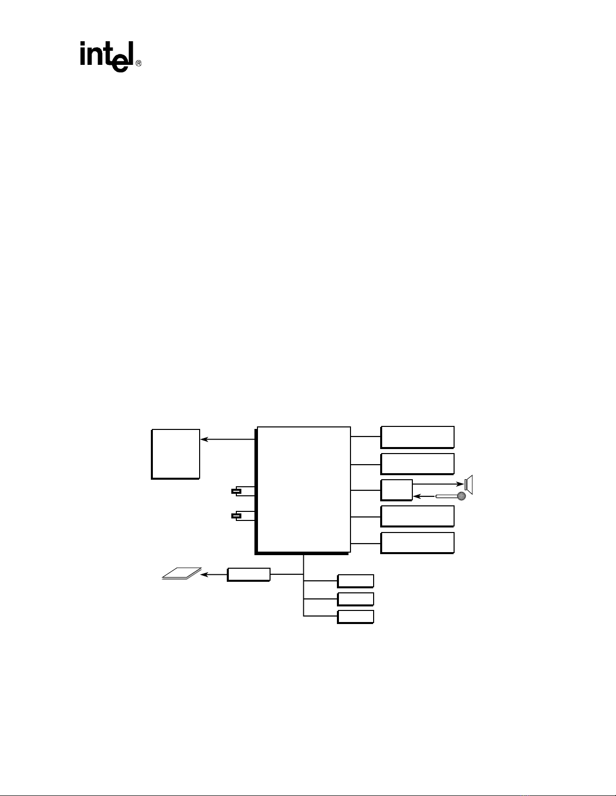
Introduction
The instruction set comprises eight basic instruction types:
• Two make use of on-chip arithmetic logic unit, barrel shifter, and multiplier to perform
high-speed operations on data in a bank of 16 logical registers (31 physical registers), each 32
bits wide.
• Three classes of instructions control data transfer between memory and the registers: one
optimized for flexibility of addressing, one for rapid context switching, and one for swapping
data.
• Two instructions control the flow and privilege level of execution.
• One class is used to access the privileged state of the CPU.
The ARM instruction set is a good target for compilers of many different high-level languages.
Where required for critical code segments, assembly code programming is also straightforward,
unlike some RISC processors that need sophisticated compiler technology to manage complicated
instruction interdependencies.
The SA-1100 is a static part and has been desi gned t o ru n at a reduced v olt age to mi nimize i ts power
requirements. This makes it a good choice for portable applications where both of t hese features are
essential.
1.3 Example System
Figure 1-2 shows how the SA-1100 can be used in a hand-held computing device.
Figure 1-2. SA-1100 Example System
Gray Scale
or
Color LCD
Display
3.686
MHz
32.768
KHz
Glue Logic
PCMCIA Interface
(Flash, Modem)
Intel® StrongARM
SA-1100
Portable
Communications
Microcontroller
®*
UART or LocalTalk
Communications
Tablet / Serial
Keyboard
Codec
Infrared
Communications
USB Synchronization
Port
DRAM
ROM
Flash
* StrongARM is a registered trademark of ARM Limited.
A6870-01
SA-1100 Developer’s Manual 1-5
Page 26

Introduction
1.4 ARM™ Architecture
The SA-1100 implements th e ARM V4 architecture as defined in the ARM Architectur e Reference,
28-July-1995, with the foll owing options:
1.4.1 26-Bit Mode
The SA-1100 supports 26-bit mode but all exceptions are initiated in 32-bit mode. The P and D bits
do not affect the operation of SA-1100; they are always read as ones and writes to them are
ignored.
1.4.2 Coprocessors
The SA-1100 supports MCR and MRC access to coprocessor number 15. These instructions are
used to access the memory-management, configuration, and cache control registers. In addition,
coprocessor 15 provides control for read buffer fills and flushes, and hardware breakpoints. All
other coprocessor instructions cause an undefined instruction exception. No support for external
coprocessors is provide d.
1.4.3 Memory Management
Memory management exceptions preserve the base address registers so that no code is required to
restore state. Separate translation lookaside buffers (TLBs) are implemented for the instruction and
data streams. Each TLB has 32 entries that can each map a segment, a large page, or a small page.
The TLB replacement algorithm is round robin. Th e data TLBs support both the flush-all and
flush-single-entry operations, while the instruction TLBs support only the flush-all operation.
1.4.4 Instruction Cache
The SA-1100 has a 16 Kbyte instruction cache (Icache) with 32-byte blocks and 32-way
associativity. The cache supports the flush-all function. Replacement is round robin within a set.
The Icache can be enabled while memory management is disabled. When memory management is
disabled, all memory is considered cacheable by the Icache.
1.4.5 Data Cache
The SA-1100 has an 8 Kbyte data cache (Dcache) with 32-byte blocks and 32-way associativity.
The cache supports the flush-all, flush-entry, and copyback-entry functions. The copyback-all
function is not supported in hardware. This function can be provided by software. The cache is read
allocate with round-robin replacement.
The Dcache has been augmented with a 16-entry, two-way set associative minicache that allocates
when the MMU b and c bits are 0 and 1, respectively. This cache is accessed in parallel with the
main Dcache. Replacement victims in this cache are replaced based on a least-recently-used (LRU)
algorithm. This cache is useful for applications that access large data structures and would
normally thrash the main Dcache. Instead, these data structur es can be mapp ed so that they allocate
into the minicache and only replace data from the same structure.
1-6 SA-1100 Developer’s Manual
Page 27

1.4.6 Write Buffer
The SA-1100 has an eight-entry write buffer with each entry able to contain 1 to 16 bytes. A drain
write buffer operation is supported.
1.4.7 Read Buffer
The SA-110 0 has a four-entry read buffer capable of loadin g 1, 4, or 8 word s of d ata per entr y. This
facility permits software to preload data into the buffer for use at a later time without block ing the
operation of the processor. Software can flush either a single entry or the entire buffer (four
entries). The read buffer is controlled through system control coprocessor 15 and can be enabled
for use in user mode.
Introduction
SA-1100 Developer’s Manual 1-7
Page 28

Page 29

Functional Description
This chapter provides a functional description of the Intel® StrongARM® SA-1100 Micropro cessor
(SA-1100). It describes the basic building blocks within the processor, lists and describes the pins,
and explains the memory map.
2.1 Block Diagram
The SA-1100 consists of the following functional blocks:
• Processor
The processor is the ARM™
(Dcache). The instruction (I) and data (D) streams are translated through independent
memory-management units (MMUs). Stores are made using a four-line write buffer. The
performance of specialized load routines is enhanced with the four-entry read buffer that can be
used to prefetch data for use at a later time. A 16-entry minicache provides a smaller and logically
separate data cache that can be used to enhance caching performance when dealing with large data
structures.
• Memory and PCMCIA controller
The memory and PCMCIA control module (MPCM) supports four banks of standard or EDO DRAM
on a 32-bit data width. ROM (standard and burst), Flash memory, and SRAM are also supported.
ROM and Flash can be either 16 or 32 bits wide. SRAM width is limited to 32 bits. Expansion devices
are supported through PCMCIA control signals that share the memory bus data and address lines to
complete the card i nter f ace. So me ex ter nal g l ue lo gic ( bu ffers and transceivers) is necessary to
implement the interface. Control is provided to permit two card slots with hot-swap capability.
• Peripherals
SA-1 core with a 16 Kbyte instruction and 8 Kbyte data cache
2
The peripheral control module (PCM) contains a number of serial control devices, an LCD
controller as well as a six-channel DMA controller to provide service to these devices:
– An LCD controller with support for passive or active displays
– A universal serial bus (USB) endpoint controller
– An SDLC communications controller
– A serial controller with supporting 115 Kbps and 4 Mbps IrDA protocols
– A 16550-like UART supporting 230 Kbps
– A CODEC interface supporting SPI, µWire, TI, UCB1100, and UCB12 00
• General system control functions
The system control module (SCM) is also connected to the peripheral bus. It contains five blocks
used for general system functions:
– A real-time clock (RTC) clocked from an independent 32.768 kHz oscillator
– An operating system timer (OST) for general system timer functions as well as a watchdog mode
– Twenty-eight general-purpose I/Os (GPIO)
– An interrupt controller
– A power-manag em en t co n tro ller th at handles the transitions in and out of slee p an d idle modes
– A reset controller that handles the various reset sources on the processor
SA-1100 Developer’s Manual 2-1
Page 30
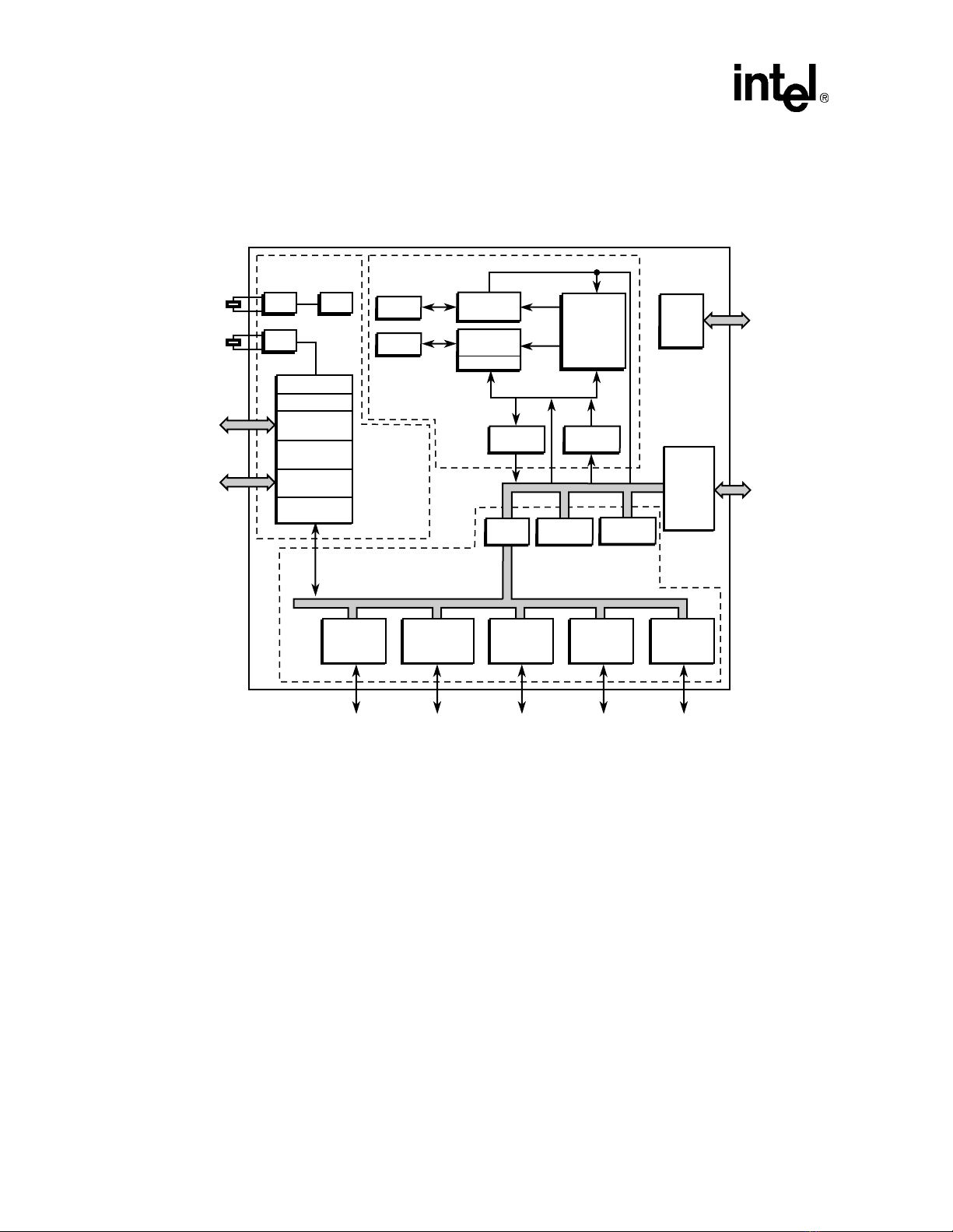
Functional Description
Figure 2-1 shows the functional blocks contained in the SA-1100 integrated proces sor. Figure 2-2
is a functional diagram of the SA-1100.
Figure 2-1. SA-1100 Block Diagram
3.686
MHz
32.768
KHz
OSC
OSC
PLL
RTC
OS Timer
General-
Purpose I/O
Interrupt
Controller
Power
Management
Reset
Controller
IMMU
DMMU
Processing
Core
System
System Bus
Control
Module
(SCM)
Peripheral Control
Module (PCM)
Peripheral Bus
Instruction
Icache
(16 Kbytes)
Dcache
(8 Kbytes)
Minicache
Load/Store Data
Write
Buffer
Bridge
PC
Addr
DMA
Controller
ARM™*
SA-1
Core
Read
Buffer
LCD
Controller
®
Intel
StrongARM
SA-1100
JTAG
and
Misc
Test
Memory
and
PCMCIA
Control
Module
(MPCM)
®
*
Serial
Channel 0
UjSB
Serial
Channel 1
SDLC
Serial
Channel 2
IrDA
Serial
Channel 3
UART
* ARM is a trademark and StrongARM is a registered trademark of ARM Limited.
Serial
Channel 4
CODEC
A6832-01
2-2 SA-1100 Developer’s Manual
Page 31

2.2 Inputs/Outputs
Figure 2-2. SA-1100 Functional Diagram
Functional Description
Serial
Channel 0
(USB)
Serial
Channel 1
(SDLC)
Serial
Channel 2
(IrDA)
Serial
Channel 3
(UART)
Serial
Channel 4
(CODEC)
Power
Management
Clocks, Reset
and Test
UDC-
UDC+
RXD _1
TXD_1
RXD _2
TXD _2
RXD _3
TXD _3
TXD _C
RXD _C
SCLK _C
SFRM _C
BATT_FAULT
VDD_FAULT
PWR_EN
TCK_BYP
TESTCLK
PEXTAL
PXTAL
TEXTAL
TXTAL
nRESET
nRESET_OUT
ROM_SEL
®
Intel
StrongARM
SA-1100
[208-pins]
®*
L_DD(7:0)
L_FCLK
L_LCLK
L_PCLK
L_BIAS
GP(27:0)
nCAS(3:0)
nRAS/(3:0)
nOE
nWE
nCS(3:0)
nPOE
nPWE
nPIOR
nPIOW
nPCE<2:1>
PSKTSEL
nPREG
nPWAIT
nIOIS16
A<25:0>
LCD
Control
GPIO
Ports
Memory
Control
PCMCIA
Bus
Signals
Address
Bus
TCK
TDI
JTAG
* StrongARM is a registered trademark of ARM Limited.
SA-1100 Developer’s Manual 2-3
TDO
TMS
nTRST
D<31:0>
VDD
VDDX
VSS/VSSX
Data Bus
Supply
A6975-01
Page 32

Functional Description
2.3 Signal Description
The following table describes the signals.
Key to Signal Types: n – Active low signal
IC – Input, CMOS threshold
ICOCZ – Input, CMOS threshold, output CMOS levels, tristatable
Table 2-1. Signal Descriptions (Sheet 1 of 3)
Name Type Description
OCZ – Output, CMOS levels, tristatable
A<25:0> OCZ Memory address bus. This bus signals the address requested for memory
D<31:0> ICOCZ Memory data bus.
nCS<3:0> OCZ Static chip selects. These signals are chip selects to static memory devices such
nOE OCZ Memory output enable. This signal should be connected to the output enables to
nWE OCZ DRAM write enable. This signal should be connected to the DRAM write enables
nRAS<3:0> OCZ DRAM RAS. These signals should be connected to the DRAM row address strobe
nCAS<3:0> OCZ DRAM CAS. These signals should be connected to the DRAM column address
nPOE OCZ PCMCIA output enable. This PCMCIA signal is an output and is used to perform
nPWE OCZ PCMCIA write enable. This signal is an output and is used to perform write s to
nPIOW OCZ PCMCIA I/O write. This signal is an output and is used to perform write
nPIOR OCZ PCMCIA I/O read. This signal is an output and is used to perform read
nPCE<2:1> OCZ PCMCIA card enable. These signals are output and are used to select a PCMCIA
nIOIS16 IC I/O Select 16. This signal is an input and is an acknowledgment from the PCMCIA
nPWAIT IC PCMCIA wait. This signal is an input and is driven low by the PCMCIA c ard to
PSKTSEL OCZ PCMCIA socket select. This signal is an output and is used by external steering
nPREG OCZ PCMCIA register select. This signal is an output and indicates that, on a memo ry
L_DD<7:0> OCZ LCD controller display data.
accesses.
Bits 21..10 carry the 12-bit DRAM address, the static memory devices, and the
expansion bus receive address bits 25..0.
as ROM and Flash. They are individually programmable in the memory
configuration registers.
begin driving data onto the data bus.
to perform writes. This signal is used in conjunction with CAS<3:0> to perform
byte writes.
(RAS) pin.
strobe (CAS) pins.
reads from memory and attribute space.
memory and attribute space.
transactions to the PCMCIA I/O space.
transactions from the PCMCIA I/O space.
card. Bit one enables the high-byte lane and bit zero enables the low-byte lane.
card that the current address is a valid 16-bit wide I/O address.
extend the length of the transfers to/from the SA-1100.
logic to route control, address, and data signals to one of the PCMCIA sockets.
When PSKTSEL is low, socket zero is selected. When PSKTSEL is high, socket
one is selected. This signal has the same timing as the address lines.
transaction, the target address is attribute space. This signal has the same timing
as address.
2-4 SA-1100 Developer’s Manual
Page 33

Table 2-1. Signal Descriptions (Sheet 2 of 3)
Name Type Description
L_FCLK OCZ LCD frame clock.
L_LCLK OCZ LCD line clock.
L_PCLK OCZ LCD pixel clock.
L_BIAS OCZ LCD ac bias drive.
TXD_C OCZ CODEC transmit.
RXD_C IC CODEC receive.
SCLK_C OCZ CODEC clock.
SFRM_C OCZ CODEC frame signal.
UDC+ OCZ Serial port zero transmit pin (UDC).
UDC- IC Serial port zero receive pin (UDC).
TXD_1 OCZ Serial port one transmit pin (SDLC).
RXD_1 IC Serial port one receive pin (SDLC).
TXD_2 OCZ Serial port two transmit pin (IrDA).
RXD_2 IC Serial port two receive pin (IrDA).
TXD_3 OCZ Serial port three transmit pin (UART).
RXD_3 IC Serial port three receive pin (UART).
GP<27:0> ICOCZ General-purpose input output.
ROM_SEL IC ROM select. This pin is used to configure the ROM width. It is either grounded or
pulled high. If ROM_SEL is grounded, the ROM width is 16 bits. If ROM_SEL is
pulled up, the ROM width is 32 bits.
PXTAL IC Input connection for 3.686-MHz crystal.
PEXTAL OCZ Output connection for 3.686-MHz crystal.
TXTAL IC Input connection for 32.768-kHz crystal.
TEXTAL OCZ Output connection for 32.768-kHz crystal.
PWR_EN OCZ Power enable. Active high. PWR_EN enables the external power supply.
Negating it signals the power supply that the system is going into sleep mode and
that the VDD power supply should be removed.
BATT_FAULT IC B attery fault. Signals the SA-1100 that the main power source is going away
(battery is low or has been removed from the system). The assertion of
BATT_FAULT causes the SA-1100 to enter sleep mode. The SA-1100 will not
recognize a wake-up event while this signal is asserted.
VDD_FAULT IC VDD fault. Signals the SA-1100 that the main power supply is going out of
regulation (shorted card is inserted). VDD_FAUL T will cause the SA-1100 to enter
sleep mode. VDD_FAULT is ignored after a wake-up event until the poser supply
timer completes (approximately 10 ms).
nRESET IC Hard reset. This active low signal is a level-sensitive input used to start the
processor from a known address. A low level will cause the current instruction to
terminate abnormally, and the on-chip caches, MMU, and write buffer to be
disabled.
When nRESET is driven high, the processor will restart from address 0. nRESET
must remain low until the power supply is stable and the internal 3.686-MHz
oscillator has come up to speed. While nRESET is low, the processor will perform
idle cycles.
Functional Description
SA-1100 Developer’s Manual 2-5
Page 34

Functional Description
Table 2-1. Signal Descriptions (Sheet 3 of 3)
Name Type Description
nRESET_OUT OCZ Reset out. This signal is asserted when nRESET is asserted and deasserts when
the processor has completed resetting. nRESET_OUT is also asserted for "soft"
reset events (sleep and watchdog).
nTRST IC Test interface reset. Note this pin has an internal pull-down resistor and must be
driven high to enable the JTAG circuitry. If left unconnected, this pin is pulled low
and disables JTAG operation.
TDI IC JTAG test interface data input. Note this pin has an internal pull-up resistor.
TDO OCZ JTAG test interface data output. Note this pin does
resistor.
TMS IC JTA G test interface mode select. Note this pin has an internal pull-up resistor.
TCK IC JTAG test interface reference clock. This times all the transfers on the JTAG test
interface. Note this pin has an internal pull-down resistor.
TCK_BYP IC T est cl ock PLL bypass. When TCK_BYP is high, the TESTCLK is used as the
core clock in place of the PLL clock; when low, the internal PLL output is used.
This signal has no relation to the JTAG TCK pin.
TESTCLK IC Test clock. TESTCLK is used to provide the core clock when TCK_BYP is high. It
should be tied low if TCK_BYP is low. This pin should be used for test purposes
only. An end user should gr ound this pin.
VDD — Positive supply for the core. Nine pins are allocated to this supply ; eight pins are
labeled VDD. The ninth pin, labeled VDDP is dedicated to the PLL supply and
should be tied directly to the VDD power plane with the other eight VDD pins.
VDDX — Positive supply for the pins. Twenty pins are allocated to VDDX, labeled VDDX1,
VDDX2 and VDDX3. All of these pins should be tied directly to the VDDX power
plane.
VSS — Ground supply. Nine pins are allocated to VSS, including one for the PLL.
VSSX — G r ound supply for the I/O pins. Eighteen pins are allocated to VSSX.
not
have an internal pull-up
2-6 SA-1100 Developer’s Manual
Page 35

2.4 Memory Map
Figure 2-3 shows the SA-1100 memory map. The map is d ivided into four main partitions of
1 Gbyte each.
The bottom partition is dedicated to static memory devices (ROM , SRAM, an d Flash) and to the
PCMCIA expansion bus area. It occupies addresses 0h0000 0000 through 0h3FFF FFFF. This
space is divided into four 128 Mbyte blocks for static memory devices and two 256 Mbyte blocks
for PCMCIA.
The static memory space is intended for ROM, SRAM, and Flash memory . The b ottom partition (at
0h0000 0000) is assumed to be ROM at boot time. The width of the boot ROM is determined by
the state of the ROMSEL pin. The PCMCIA interface is divided into Socket 0 and Socket 1 space.
These partitions are further subdivided into I/O, memory and attribute space.
The next partition (0h4000 0000 to 0h7FFF FFFF) is reserved. Accessing this reserved space
results in a data abort exception.
Functional Description
The third partition (0h8000 0000 to 0hBFFF FFFF) con tains all on-chip registers (except those
specified by the ARM
256 Mbyte each. They contain control registers for the major functional blocks within the
processor (MECM, SCM, PCM). The LCD and DMA controllers are separate from the rest of the
PCM and occupy the top 256 Mbyte partition.
The fourth partition (0hC000 0000 to 0hFFFF FFFF) contains DRAM memory. The bank sizes for
DRAM are fixed at 128 Mbyte each. With multiple banks implemented, there probably will be
gaps in the map that should be map ped through the memory-management un it. The next 128 Mbyte
block in this partition is mapped within the memory controller and returns zeros when read. This
function is intended to facilitate rapid cache flushing by not requiring an external memory access to
load data into the cache. This space is burstable. Writes to this space have no effect. The top
384 Mbyte of this partition is reserved. Accessing this space causes a data abort exception.
V4 architecture). This block is further subdivided in to four blocks of
SA-1100 Developer’s Manual 2-7
Page 36

Functional Description
Figure 2-3. SA-1100 Memory Map
Reserved (384 Mbyte)
0hC000 0000
0h8000 0000
0h4000 0000
0h2000 0000
0h0000 0000
Zeros Bank (128 Mbyte)
DRAM Bank 3 (128 Mbyte)
DRAM Bank 2 (128 Mbyte)
DRAM Bank 1 (128 Mbyte)
DRAM Bank 0 (128 Mbyte)
LCD and DMA Registers (256 Mbyte)
Memory and Expansion Registers (256 Mbyte)
System Control Module Registers(256 Mbyte)
Peripheral Module Registers (256 Mbyte)
Reserved (1GB)
PCMCIA Socket 0 Space (256 Mbyte)
PCMCIA Socket 1 Space (256 Mbyte)
Static Bank Select 3 (128 Mbyte)
Static Bank Select 2 (128 Mbyte)
Static Bank Select 1 (128 Mbyte)
Static Bank Select 0 (128 Mbyte)
Cache flush replacement data
Reads return zero
128 Mbyte
Dynamic Memory
512 Mbyte
Internal Registers
1GB
PCMCIA Interface
512 Mbyte
Static Memory
(ROM, Flash, SRAM)
512 Mbyte
2-8 SA-1100 Developer’s Manual
Page 37

ARM
™
Implementation Options
The following sections describe ARM™ architecture options that are implemented by the
®
StrongARM® SA-1100 Microprocessor (SA-1100).
Intel
3.1 Big and Little Endian
The big endian bit in the control register sets whether the SA-1100 treats words stored in memory
as being stored in big endian or little endian format. Mem ory is viewed as a linear collection of
bytes numbered upwards from 0. Bytes 0 to 3 hold the first stored word, bytes 4 to 7 hold the
second, and so on.
In the little endian scheme, the lowest numbered byte in a word is con sidered to be the least
significant byte of the word and the highest numb ered by te is the most significant. Byte 0 of the
memory system should be connected to data lines 7 through 0 (D<7:0>) in this scheme.
In the big endian scheme, the most sign if icant b yte of a word is stored at the lowest numbered byte
and the least significant byte is stored at the highest numbered byte. Therefore, byte 0 of the
memory system should be connected to data lines 31 through 24 (D<31:24>).
The state of the big endian bit changes the location of the bytes only within a 32-bit word. The
accessed bytes are changed for the load byte, store byte, load halfword, and store halfword
instructions only. Instruction fetches and word load and stores are not changed by the state of the
big endian bit, except when those accesses are performed with memory on 16-bit data busses. See
Chapter 10 for details on configuring bus widths for various memory types.
3
These conventions are identical to those of the SA-110. In addition, the SA-1100 DMA controller
is programmable by channel as to the endian format of the transfer. For DMA transfers, all
memory accesses are words. Then the data is buffered and transferred to/fro m the device as
halfwords or bytes. When the words are assembled or disassembled, the endian format of the
channel is observed. For details on how DMA data is transferred relative to the endian format of
the channel, see the Section 11.6, “DMA Contr oller” on page 11-7 in Chapter 11, “Peripheral
Control Module”.
3.2 Exceptions
Exceptions arise whenever there is a need for the normal flow of program execution to be broken;
for example, so that the processor can be diverted to handle an interrupt from a peripheral. The
processor state just prior to handling the exception must be preserved so that the original program
resumes when the exception routine has completed. Many exceptions may arise at the same time.
The SA-1100 handles exceptions by making use of banked registers to save state. The contents of
PC and CPSR are copied into the appropriate R14 and SPSR, and the PC and mode bits in the
CPSR bits are forced to a value that depends on the exception . In terrup t disa ble flags are set where
required to prevent otherwise unmanageable nestings of exceptions. In the case of a reentrant
interrupt handler, R14 and the SPSR should be saved onto a stack in main memory before
reenabling the interrupt; when transferring t he SPSR register to and from a stack, it is important to
SA-1100 Developer’s Manual 3-1
Page 38

ARM™ Implementation Options
transfer the whole 32-bit value, and not just the flag o r control fields. When multiple exceptions
arise simultaneously, a fixed priority determines the order in which they are handled. The priorities
are listed later in this chapter. Most exceptions are fully defined in the ARM Architectural
Reference. The following sections specify the exceptions where the SA-1100 implementation
differs from the ARM Architectural Reference.
SA-1100 initiates all exceptions in 32-bit mode. When an exception occurs while running in 26-bit
mode, the SA-1100 sa ves only the PC in R14 and the CPSR in the SPSR of the exception mode.
The 32-bit handler must merge the condition codes, the interrupt enables, and the mode from the
SPSR into R14 if a handler is to run in 26-bit mode.
3.2.1 Power-Up Reset
When the nRESET signal is low, SA-1100 stops executing instructions, as serts the nRESET_OUT
pin, and then performs idle cycles on the bus.
When nRESET is high again, SA-1100 does the following:
1. Overwrites R14_svc and SPSR_svc by copying the current values of the PC and CPSR into
them. The values of the saved PC and CPSR are not defined.
2. Forces M<4:0>=10011 (32-bit supervisor mode) and sets the I and F bits in the CPSR.
3. Forces the PC to fetch the next instruction from address 0x0000 0000.
4. Based on the state of the ROM_SEL pin, fetches this first instruction from either 16 -bit
(ROM_SEL low) or 32-bit (ROM_SEL high) space. The SA-1100 memory controller
assembles the data into words in the case of a 16-bit wide ROM.
At the end of the reset sequence, the MMU, Icache, Dcache, and write buffer are disabled.
Alignment faults are also disabled, and little-endian mode is enabled. During power-up, nRESET
must be negated no earlier than 150 milliseconds after VDD and VDDx are stable to allow the
internal 3.686-MHz oscillator to stabilize. After the negation of nRESET, the PLL begins its
internally timed locking sequence. Note that the assertion of nRESET is destructive because the
state of the real-time clock and the contents of DRAM are lost.
The SA-1100 has three types of reset. See Section 16.2, “Reset” on page 16-2 in the
Boundary-Scan Test Interface for details.
3.2.2 ROM Size Select
The ROM width may be sel ected using the ROM_SEL p in. This pin is sampled during t he asserti on
of nRESET. The value is stored in the memory controller for use during ROM accesses. If this
signal is high during RESET, then the ROM is selected to be 32 bits wide. If it is low during
RESET, then the ROM width is 16 bits. There is no provision for 8-bit ROMs in the SA-1100.
3-2 SA-1100 Developer’s Manual
Page 39

3.2.3 Abort
An abort can be signalled by the internal memory-management unit, through a data breakpoint, or
by a reference to reserved memory. An abort indicates that the current memory access cannot be
completed or that a prespecified breakpoint address and (optionally) data patter n has been reached.
For instance, in a virtual memory system, the data corresponding to the current address may have
been moved out of memory onto a disk, and considerable processor activity may be required to
recover the data before the access can be performed successfully . The SA-1 1 00 checks for an abor t
during memory access cycles. When aborted, the SA-1100 responds in one of two ways:
1. If the abort occurred during an instruction prefetch (a prefetch abort), the prefetched
instruction is marked as invalid but the abort exception does not occur immediately. If the
instruction is not executed, for example, as a result of a branch being taken while it is in the
pipeline, no abort will occur . An abort will take place if the instruction reaches the head of the
pipeline and is about to be executed.
2. If the abort occurred during a data access (a data abort), the action depends on the instruction
type.
a. Single data transfer instructions (LDR, STR) will abort with no registers modified.
b. The swap instruction (SWP) is aborted as though it had not executed, though externally
c. Block data transfer instructions (LDM, STM) abort on the first access that cannot
ARM™ Implementation Options
the read access may take place.
complete. If write-back is set, the base is NOT updated. If the instruction would normally
have overwritten the base with data (for example, an LDM instruction with the base in the
transfer list), the original value in the base register is restored.
When either a prefetch or data abort occurs, the SA-1100 performs the following:
1. Saves t he address of th e abo rted ins truc tion plu s 4 (f or prefetch aborts) or 8 (for data aborts) in
R14_abt; saves CPSR in SPSR_abt.
2. Forces M<4:0>=10111 (abort mode) and sets the I bit in the CPSR.
3. Forces the PC to fetch the next instruction from either add ress 0x0C (prefetch ab ort) or addr ess
0x10 (data abort).
To return after fixing the reason for the abort, use SUBS PC,R14_abt,#4 (for a prefetch abort) or
SUBS PC,R14_abt,#8 (for a data abort). This will restore both the PC and the CPSR, and retry the
aborted instruction.
The abort mechanism allows a demand paged virtual memory system to be implemented when
suitable memory management so ftware is avai l abl e. The pr oces so r is al lo wed t o gener ate arbitrary
addresses, and when the data at an address is unavailable, the MMU signals an abort. The processor
traps into system software, which must work out the cause of the abort, make the requested data
available, and retry the aborted instruction. The application program needs no knowledge of the
amount of memory available to it, nor is its state in any way affected by the abort.
SA-1100 Developer’s Manual 3-3
Page 40

ARM™ Implementation Options
3.2.4 V ector Summary
Table 3-1 lists byte addresses, and they normally contain branch instructions pointing to the
relevant routines. These addresses (except the reset vector) can be changed (to 0xFFFF xxxx)
through the vector adjust facility (bit 13, register 1, coprocessor 15). The vector adjust is cleared at
Table 3-1. Vector Summary
reset and cannot modify the reset vector.
Address Exception Mode on Entry
0x00000000 Reset Supervisor
0x00000004 Undefined instruction Undefined
0x00000008 Software interrupt Supervisor
0x0000000C Abort (prefetch) Abort
0x00000010 Abort (data) Abort
0x00000014 Not used —
0x00000018 IRQ IRQ
0x0000001C FIQ FIQ
3.2.5 Exception Priorities
When multiple exceptions arise at the same time, a fixed priority system determines the order in
which they will be handled:
1. Reset (highest priority)
2. Data abort
3. FIQ
4. IRQ
5. Prefetch abort
6. Undefined instruction, so ftware interrupt (lowest priority)
Note that not all exceptions can occur at once. Undefined instructions and software interrupts are
mutually exclusive because they correspond to particular (nonoverlapping) decodings of the
current instruction.
If a data abort occurs at the same time as a FIQ, and FIQs are enabled (that is, the F flag in the
CPSR is clear), the SA-1100 will enter the data abort handler and then immediately proceed to the
FIQ vector. A normal return from FIQ will cause the data abort handler to resume execution.
Placing data abort at a higher priority than FIQ is necessary to ensure that the transfer error does
not escape detection; the time for this exception entry should be added to worst-case FIQ latency
calculations.
3-4 SA-1100 Developer’s Manual
Page 41

3.2.6 Interrupt Latencies and Enable Timing
The ability to recognize an IRQ or FIQ interrupt is, in part, determined by the I and F bits of the
CPSR. To ensure that a pending interrupt is taken, an interrupt-enabling write to CPSR (msr
instruction) must be separated from an interrupt-disabling write to the CPSR by at least two
instructions.
3.3 Coprocessors
The SA-1100 has no external coprocessor bus, so it is not possible to add external coprocessors to
this device.
The SA-1100 uses the inter nal cop rocessor d esig nated 15 f or co ntro l of th e on- chip MMU, caches,
clocks, and breakpoints. Coprocessor 15 is also used for read-buffer fills and flushes. If a
coprocessor other than 15 is used, then the SA-1100 will take the undefined instruction trap. The
coprocessor load, store, and data operation instructi ons also take the undefined instruction trap.
Permissions are set so that access to coprocessor 15 is privileged except where prot ection is
programmable with respect to the read buffer operations.
ARM™ Implementation Options
SA-1100 Developer’s Manual 3-5
Page 42

Page 43

Instruction Set
This section describes the instruction timing for the Intel® StrongARM® SA-1100 Micr oprocessor
(SA-1100).
4.1 Instruction Set
The SA-1100 implements the ARM™ V4 architecture as defined in the ARM Architecture
Reference, 28-July-1995, with previously noted options and additions.
4.2 Instruction Timings
Table 4-1 lists the instruction timing for the SA-1100. The result delay is the number of cycles that
the next sequential instruction would stall if it used the result as an input. The issue cycles are the
number of cycles that this instruction takes to is sue. For most instructions, the result delay is zero
and the issue cycles is one. For load and stores, the timing is for cache hits.
Table 4-1. Instruction Timings
Instruction Group Result Delay Issue Cycles
4
Data processing 0 1
Mul or Mul/Add giving 32-bit result 1..3 1
Mul or Mul/Add giving 64-bit result 1..3 2
Load single – write-back of base 0 1
Load single – load data zero extended 1 1
Load single – load data sign extended 2 1
Store single – write-back of base 0 1
Load multiple (delay for last register) 1
Store multiple – write-back of base 0
Branch or branch and link 0 1
MCR 2 1
MRC 1 1
MSR to control 0 3
MRS 0 1
Swap 2 2
MAX
(2, number of registers loaded)
MAX
(2, number of registers loaded)
SA-1100 Developer’s Manual 4-1
Page 44

Page 45

Coprocessors
The operation and configuration of the Intel® StrongARM® SA-1100 Microproces sor (SA-1 100) is
controlled with coprocessor instructions, configuration pins, and memory-management page
tables. The coprocessor 15 instructions manipulate on-chip registers that control the configuration
of the cache, write buffer, MMU, read buffer, breakpoints, and other configuration options.
Note: The gray areas in the register and translation diagrams are reserved and should be programmed 0
for future compatibility.
5.1 Internal Coprocessor Instructions
The on-chip cache, MMU, write buf fer , and read buf fers are con trolled using MRC in structions and
MCR instructions. These operations to coprocessor 15 are allowed only in nonuser modes except
when read-buffer operations are explicitly enabled. The undefined instru ction trap is taken if
accesses are attempted in user mode. Figure 5-1 shows the format of internal coprocessor
instructions MRC and MCR.
Figure 5-1. Format of Internal Coprocessor Instructions MRC and MCR
Cond
1110 n 1111 1
CRn Rd
5
034578111215161920212324272831
OPC_2 CRm
Cond ARM™
n 1 MRC register read
0 MCR register write
CRn SA-1100 register
Rd ARM register
OPC_2 Function bits for some MRC/MCR instructions
CRm Function bits for some MRC/MCR instructions
condition codes
SA-1100 Developer’s Manual 5-1
Page 46

Coprocessors
5.2 Coprocessor 15 Definition
The SA-1100 coprocessor 15 contai ns registers that control the cache, MMU, and write buffer
operation as well as some clocking functions. These registers are accessed using CPRT instr uctions
to coprocessor 15 with the processor in any privileged mode. Only some of registers 0–15 are
valid; the result of an access to an invalid register is unpredictable. Table 5-1 lists the coprocessor
15 control registers.
Table 5-1. Cache and MMU Control Registers (Coprocessor 15)
Register Register Reads Register Writes
0ID
1
2
3
4
5
6
7
8
9
10..12 RESERVED RESERVED
13 Read process ID (PID) Write process ID (PID)
14 Read breakpoint Write breakpoint
15 RESERVED Test, clock, and idle
Control Control
Translation table base Translation table base
Domain access control Domain access control
RESERVED RESERVED
Fault status Fault status
Fault address Fault address
RESERVED Cache operations
RESERVED TLB operations
RESERVED Read buffer operations
5.2.1 Register 0 – ID
Register 0 is a read-only register that returns an architecture and implementation-defined
identification for the device.identification for the device.
44 Stepping
Architecture Version
RESERVED
0341516232431
Part Number
Architecture Version
ARM architecture version
01 = Version 4
Part Number
Part number
A11 = SA1100
Stepping
Stepping revision of SA -1100
1 = B stepping
2 = C stepping
8 = D stepping
9 = E stepping
11 = G stepping
5-2 SA-1100 Developer’s Manual
Page 47

5.2.2 Register 1 – Control
Register 1 is a read/write register containing control bits. All writable bits in this register are forced
low by reset. The shaded bits (also labeled r) are reserved and are not readable or writable.
Coprocessors
13
12
rrrrrrrrrrrrrrrrrrXIrrRSB111W ACM
M bit 0 Enable/disable
0 – On-chip memory-management unit disabled
1 – On-chip memory-management unit enabled
A bit 1 Address fault enable/disable
0 – Alignment fault disabled
1 – Alignment fault enabled
C bit 2 Data cache enable/disable
0 – Data cache disabled
1 – Data cache enabled
W bit 3 Write buffer enable/disable
0 – Write buffer disabled
1 – Write buffer enabled
B bit 7 Big/little endian
0 – Little endian operation
1 – Big endian operation
S bit 8 System
This bit selects the access checks performed by the memory-management unit.
ARM Architecture Reference
See the
R bit 9 ROM
This bit selects the access checks performed by the memory-management unit.
ARM Architecture Reference
See the
I bit 12 Instruction cache enable/disable
0 – Instruction cache disabled
1 – Instruction cache enabled
X bit 13 Virtual interrupt vector adjust
0 – Base address of interrupt vectors is 0h0000 0000
1 – Base address of interrupt vectors is 0hFFFF 0000
Bits 14..31 Unused.
Undefined on Read. Writes ignored.
for more information.
for more information.
012345678931
SA-1100 Developer’s Manual 5-3
Page 48

Coprocessors
5.2.3 Register 2 – Translation Table Base
Register 2 is a read/write register that holds the base of the currently active level 1 page table. Bits
<13:0> are undefined on read, ig nored on write.
Translation Table Base
5.2.4 Register 3 – Domain Access Control
Register 3 is a read/write register that holds the current access control for domains 0 to 15. Refer to
the ARM Architecture Reference for a description of the domain structure
0131431
012345678910111213141516171819202122232425262728293031
0123456789101112131415
5.2.5 Register 4 – RESERVED
Register 4 is reserved. Accessing this register yields unpredictable results.
5.2.6 Register 5 – Fault Status
Reading register 5 returns the current contents of th e fault status register (FSR). The FSR is wr itten
when a data memory fault occurs or can be written by an MCR to the FSR. It is not updated for a
prefetch fault. See Chapter 7, “Memory-Management Unit (MMU)” for more details. Bits
<31:10> are undefined on read, ignored on write. Bit 9 is set when a data breakpoint is taken and
can be cleared by an MCR operation. Bit 8 is ignored on writ e and is always returned as zero.
Refer to the ARM Architectur e Reference for a description of the domain and status fields.
31
5.2.7 Register 6 – Fault Address
Reading register 6 returns the current contents of the fault addres s register (FAR). The FAR is
written when a data memory fault occurs with the virtual address of the data fault or can be written
by an MCR to the FAR.
10
9
0 Domain Status
D
03478
031
Fault Virtual Address
5-4 SA-1100 Developer’s Manual
Page 49

5.2.8 Register 7 – Cache Control Operations
Register 7 is a write-only register. The CRm and OPC_2 fields are used to encode the cache control
operations. Operation for all other values for OPC_2 and CRm is unpredictable.
Function OPC_2 CRm Data
Flush I+D 0b000 0b0111 Ignored
Flush I 0b000 0b0101 Ignored
Flush D 0b000 0b0110 Ignored
Flush D single entry 0b001 0b0110 Virtual address
Clean Dcache entry 0b001 0b1010 Virtual address
Drain write buffer 0b100 0b1010 Ignored
5.2.9 Register 8 – TLB Operations
Register 8 is a write-only register. The CRm and OPC_2 fields are used to encode the following
TLB flush operations. Operation for all other values of OPC_2 and CRm is unpredictable.
Coprocessors
Function OPC_2 CRm Data
Flush I+D 0b000 0b0111 Ignored
Flush I 0b000 0b0101 Ignored
Flush D 0b000 0b0110 Ignored
Flush D single entry 0b001 0b0110 Virtual address
SA-1100 Developer’s Manual 5-5
Page 50

Coprocessors
5.2.10 Register 9 – Read-Buffer Operations
The read buffer is controlled and accessed through register 9 of coprocessor 15. The functions
supported are: flush-all buffers, flush-a-single entry, load-an-entry (1, 4 or 8 words), and
enable/disable user mode access.
The CRm and OPC_2 fields are used to encode these control operations. All other values for
OPC_2 and CRm are undefined and the results of using them are unpredictable.
Function OPC_2 CRm Data
Flush all entries 0b000 0b0000 Ignored
Flush Buffer 0 0b001 0b0000 Ignored
Flush Buffer 1 0b001 0b0001 Ignored
Flush Buffer 2 0b001 0b0010 Ignored
Flush Buffer 3 0b001 0b0011 Ignored
Load Buffer 0 with one word 0b010 0b0000 Virtual addres s
Load Buffer 0 with four words 0b010 0b0100 Virtual address
Load Buffer 0 with eight words 0b010 0b1000 Virtual address
Load Buffer 1 with one word 0b010 0b0001 Virtual addres s
Load Buffer 1 with four words 0b010 0b0101 Virtual address
Load Buffer 1 with eight words 0b010 0b1001 Virtual address
Load Buffer 2 with one word 0b010 0b0010 Virtual addres s
Load Buffer 2 with four words 0b010 0b0110 Virtual address
Load Buffer 2 with eight words 0b010 0b1010 Virtual address
Load Buffer 3 with one word 0b010 0b0011 Virtual addres s
Load Buffer 3 with four words 0b010 0b0111 Virtual address
Load Buffer 3 with eight words 0b010 0b1011 Virtual address
Disable user-mode MCR access 0b100 0b0000 Ignored
Enable user-mode MCR access 0b101 0b0000 Ignored
See Chapter 6, “Caches, Write Bu ffer, and Read Buffer” for details on the use and operation of the
read buffer.
5.2.11 Registers 10 – 12 RESERVED
Accessing any of these registers yields unpredictable results.
5-6 SA-1100 Developer’s Manual
Page 51

5.2.12 Register 13 – Process ID Virtual Address Mapping
The SA-1100 su pports the remapping of virtual addresses through a process ID (PID) register. The
6-bit PID value is OR’ed with bits 30..25 of the virtual address when bits 31..25 of the virtual
address are zero. This effectively remaps the address to on e of 64 “slots” in the lower 2 Gbyte
address space. The following table shows the OPC_2 and CRm field encodings used to access the
process ID register. This register is zero at reset and if left unmodified, effectively disables the
remapping function. As such, no explicit enable or disable function is necessary. Reserved bits read
as zero and must be written as zero. This register is readable and writable.
Function OPC_2 CRm
Access process ID register 0b000 0b0000
The following figure shows the format of the process ID register.
Coprocessors
r
30
Process ID
02431 25
Reserved
SA-1100 Developer’s Manual 5-7
Page 52

Coprocessors
5.2.13 Register 14 – Debug Support (Breakpoints)
The SA-1100 supports address and data breakpoints through register 14 of coprocessor 15. The
instruction formats follow. For a description of the breakpoint operation, see Chapter 15, “Debug
Support”. The following table show s the OPC_2 and CRm field encodings used to access the
address and data breakpoints.
Function OPC_2 CRm
Access data breakpoint address register (DBAR). 0b000 0b0000
Access data breakpoint value register (DBVR). 0b000 0b0001
Access data breakpoint mask register (DBMR). 0b000 0b0010
Load data breakpoint control register (DBCR).
----------------------------------------------------------------DBCR Bit Action
---------------------------------------------------------------- lw 0 = Disable load watch
1 = Enable load watch
saw 0 = Disable store address watch
1 = Enable store address watch
sdw 0 = Disable store data watch
1 = Enable store data watch
Write instruction breakpoint address and control register (IBCR).
Low-order address bit is the address break enable/disable bit.
Register not readable.
0b000 0b0011
0b000 0b1000
The DBCR register is a 3-bit register used to control the enabling and disabling of the data
breakpoints. Bits 0..2 are valid and positioned as shown below. Bits 3..31 are reserved. These bits
read as zeros and writes have no effect.
31
Reserved
2
1
0
lw
sawsdw
The IBCR is a write-only register used to load an address breakpoint address and to set an enable
bit for the function. If an address is loaded with bit 0 (E) set, then the address is enabled as a
breakpoint. If bit zero is cleared, then the breakpoint is disabled. Bit 1 is reserved and should be
written to zero.
31
Instruction Address Breakpoint Value
2
0
1
E
r
5-8 SA-1100 Developer’s Manual
Page 53

5.2.14 Register 15 – Test, Clock, and Idle Control
Register 15 is a write-only register. The CRm and OPC_2 fields are used to encode the following
control operations. Operation for all other values of OPC_2 and CRm is unpredictable.
Function OPC_2 CRm
Coprocessors
Enable odd-word loading of the linear feedback shift
register ( LFSR)
Enable even-word loading of LFSR 0b001 0b0010
Clear LFSR 0b001 0b0100
Move LFSR to R14.abort 0b001 0b1000
Enable clock switching 0b010 0b0001
Disable clock switching 0b010 0b0010
RESERVED 0b010 0b0100
Wait for interrupt 0b010 0b1000
0b001 0b0001
SA-1100 Developer’s Manual 5-9
Page 54

Page 55

Caches, Write Buffer, and Read Buffer
To reduce effective memory access time, the Intel® StrongARM® SA-1100 Microprocessor
(SA-1100) has an instruction cache, a data cache, a write buffer, and a read buffer. All except the
read buffer are transparent to program execution. The following sections describe each of these
units and give all necessary programming information.
6.1 Instruction Cache (Icache)
The SA-1100 co ntains a 1 6 Kbyte instruction cache (Icache). The Icache has 512 lines of 32 bytes
(8 words), arranged as a 32-way set associative cache, and uses the virtual addresses generated by
the processor core. The Icache is always reloaded a line at a t ime (8 words). It may be enabled or
disabled via the SA-1100 control register, and is disabled on the assertion of nRESET or through a
software or sleep reset sequence. (See Section 9, “System Control Module” on page 9-1 in the
System Control Module for details.) The operation of the cache, when memory management is
enabled, is further controlled by the cacheable or C bit stored in the memory-management page
table. If memory management is disabled, all addresses are marked as cacheable (C=1). When
memory management is enabled, the C bit in each page table entry can disable caching for an area
of virtual memory.
6.1.1 Icache Operation
6
In the SA-1100, the instruction cache is searched regardless of the state of the C bit; only reads that
miss the cache are affected. If, on an Icache miss, the C bit is a one or the Memory Management
Unit (MMU) is disabled, a linefetch of 8 words is performed and it is placed in a cache bank with a
round-robin replacement algorithm. If, on a miss, the MMU is enabled and the C bit is a zero for
the given virtual address, an external memory access for a single word is performed and the cache
is not written.The Icache should be enabled as soon as possible after reset for best performance.
6.1.2 Icache Validity
The Icache operates with virtual addresses, so care must be tak en to ensur e that its contents remain
consistent with the virtual-to-physical mappings performed by the memory management unit. If the
memory mappings are changed, the Icache validity must be ensured. The Icache is not coherent
with stores to memory, so programs that write cacheable instruction locations must ensure the
Icache validity. Instruction fetches do not check the write buffer, so data must not only be pushed
out of the cache but the write buffer must also be drained.
6.1.2.1 Software Icache Flush
The entire Icache can be invalidated by writing to the SA-1100 cache op eratio ns register (register
7). The cache is flushed immediately when the register is written, but note that the following
instruction fetches may come from the cache before the register is written.
SA-1100 Developer’s Manual 6-1
Page 56

Caches, Write Buffer, and Read Buffer
6.1.3 Icache Enable/Disable and Reset
The Icache is automatically disabled and flushed on the assertion of nRESET. Once enabled,
cacheable read accesses cause lines to be placed in the cache. If the Icache is subsequently
disabled, no new lines are placed in the cache, but the cache is still searched and if the data is
found, it will be used by the processor. If the data in the cache must not be used, then the cache
must be flushed.
6.1.3.1 Enabling the Icache
To enable the Icache, set bit 12 in the control register. The MMU and Icache may be enabled
simultaneously with a single control register write.
6.1.3.2 Disabling the Icache
To disable the Icache, clear bit 12 in the control register.
6.2 Data Caches (Dcaches)
The SA-1100 contains two logically separate data caches: the mai n data cache and the mini data
cache (or minicache). The main data cache, an 8 Kbyte write-back Dcache, has 256 lines of 32
bytes (8words) in a 32-way set-associative organization. It is intended for use during most data
accesses. This cache allocates on loads to spaces marked B=1 and C=1. Replacements in the main
data cache are selected according to a set of round-robin pointers. At reset, the pointer in each
block of the Dcache points to way zero of each 32-way block. As lines are allocated, the pointers
are incremented to the next way of the set. After way 31 is allocated, the next linefill replaces (and
copies back to memory, if dirty) the data in way zero. The minicache is a 512-byte write-back
cache. It has 16 lines of 32 bytes (8 words) in a two-way set-associative organization and provides
an alternate caching structure for dealing with large data structures that could thrash the main data
cache. This cache allocates on loads to spaces marked B=0 and C=1. Replacements in the
minicache use the same round-robin pointer mechanism as in the main data cache. However, since
this cache is only two-way set-associative, the replacement algorithm reduces to a simple
least-recently-used (LRU) mechanism.
The Dcaches are accessed in parallel and the design ensures that a particular line entry will exist in
only one of the two at any time. Both Dcaches use the virtual address generated by the processor
and allocate only on loads (write misses never allocate in the cache). Each line entry contains the
physical address of the line and two dirty bits. The dirty bits indicate the status of the first and the
second halves of the line. When a store hits in the Dcaches, the dirty bit associated with it is set.
When a line is evicted from the Dcaches, the dirty bits are used to decide if all, half, or none of the
line will be written back to memory using the physical address stored with the line. The Dcaches
are always reloaded a line at a time (8 words).
The Dcaches allocate only on loads and according to the settings of the B and C bi ts in the MMU.
If B=0 and C=1, the memory access allocates into the minicache. If B=1 and C=1, the memory
access allocates into the main data cache. The Dcaches should be flushed prior to changing the
bufferable and/or cacheable state of the page table mapping.
The main data cache and the minicache are enabled and dis abled via the SA-1100 control register,
and are disabled on nRESET as well as software, sleep, and watchdog reset. The operation of the
Dcaches is further controlled by the cacheable or C bit and the bufferable or B bit stored in the
6-2 SA-1100 Developer’s Manual
Page 57

memory-management page table. For this reason, in order to use the Dcaches, the MMU must be
enabled. The two functions may be enabled simultaneously with a single write to the control
register.
Note: The Dcaches operate with virtual addresses, so care must be taken to ensure that their contents
remain consistent with the virtual-to-physical mappings performed by the memory-management
unit. If the memory mappings are changed, the validity of the Dcaches must be ensured.
6.2.1 Cacheable Bit – C
The cacheable bit determines whether, on load misses, the data being read should be placed in one
of the two data caches. Cache hits are not affected by the cacheable bit; if a data access hits in the
cache, the data is assumed to be valid and the load or store is perf ormed. Typically, m ain memory is
marked as cacheable to improve system performance and I/O space as noncacheable to stop the
data from being stored in SA-1100’s cache. For example, if the processor is polling a hardware flag
in I/O space, it is important that the processor is forced to read data from the external peripheral,
and not a copy of initial data held in the cache.
6.2.1.1 Cacheable Reads – C = 1
A linefetch of 8 words will be performed and it will be placed in a cache bank with a round-robin
replacement algorithm.
Caches, Write Buffer, and Read Buffer
6.2.1.2 Noncacheable Reads – C = 0
An external memory access will be performed and the cache will not be written.
6.2.2 Bufferable Bit – B
The buffer able bit does not af fect writes that hit the Dcaches. If a store hits in the Dcaches, the store
is assumed to be bufferable. Write-backs of dirty lines are treated as bufferable writes. See the
Section 6.3, “Write Buffer (WB)” on page 6-5 for more information on the B bit.
Table 6-1 summarizes the effects of the B and C bits on the Dcaches.
Table 6-1. Effects of the Cacheable and Bufferable Bits on the Data Caches
Load Store
BC
0 0 Deliver cache data. Load from memory.
0 1 Deliver cache data. Allocate to minicache. Store to either cache.
1 0 Deliver cache data. Load from memory.
1 1 Deliver cache data. Allocate to main data cache. Store to either cache.
Cache Hit Cache Miss Cache Hit Cache Miss
– No allocate.
– No allocate.
Store to either cache.
– Mark line dirty.
– Mark line dirty.
Store to either cache.
– Mark line dirty.
– Mark line dirty.
Store to memory.
– No allocate.
Store to memory.
– No allocate.
Store to memory.
– No allocate.
Store to memory.
– No allocate.
SA-1100 Developer’s Manual 6-3
Page 58

Caches, Write Buffer, and Read Buffer
6.2.3 Software Dcache Flush
The SA-1100 supports the flush and clean operations on single entries of the Dcaches by writes to
the cache operations registers. The flush whole cache is also supported. Note that since this is a
write-back cache, in order to prevent the loss of data, a flush whole must be preceded by a
sequence of loads to cause the cache to write back any dirty entries. The memory controller in the
SA-1100 provid es an intern ally deco ded m e mory space to perfo rm co heren t Dcache flushing. This
space resides in the upper 512 megabytes of the memory map (starting at virtual address
0hE000 0000) and, when accessed, is detected by the memory controller, which then returns zeros
without incurring an external memory latency.
The following code causes the main data cache to flush all dirty entries:
;+
;Call:
; R0 points to the start of a 8192 byte region of readable data used
; only for this cache flushing routine.
; bl writeBackDC
;Return:
; R0, R1, R2 trashed
; Data cache is clean
;-
writeBackDC
movr0, 0hE0000000
addr1, r0, #8192
l1
ldr r2, <r0>, #32
teqr1, r0
bnel1
mcrp15, 0, r0, c7, c6, 0
movpc, r14
A similar routine may be written to flush the minicache. To p erfor m this flush , the MMU B and C
settings must be as described above. The invalidate-all operation also invalidates the minicache.
6.2.3.1 Doubly Mapped Space
Since the Dcaches work with virtual addresses, it is assumed that every virtual address maps to a
different physical address. If the same physical location is accessed by more than one virtual
address, the cache cannot maintain consistency, since each virtual address has a separate entry in
the cache, and only one entry is updated on a processor write operation. To avoid any cache
inconsistencies, doubly mapped virtual addresses should be marked as noncacheable.
6.2.4 Dcaches Enable/Disable and Reset
The Dcaches are automatically disabled and flushed on the assertion of nRESET. Once enabled,
cacheable read accesses cause lines to be placed in the Dcaches. If subsequently disabled, no new
lines are placed in the Dcaches, but they are still searched and if the data is found, it is used by the
processor. Write operations continue to update the Dcaches, thus maintaining consistency with the
external memory. If the data in the Dcaches must not be used, then the Dcaches must be flushed.
6-4 SA-1100 Developer’s Manual
Page 59

6.2.4.1 Enabling the Dcaches
To enable the Dcaches, make sure that the MMU is enabled first by setting bit 0 in the control
register, then enable the Dcaches by setting bit 2 in the control register . The MMU and Dcaches can
be enabled simultaneously with a single control register write.
6.2.4.2 Disabling the Dcaches
To disable the Dcache, clear bit 2 in the control register.
6.3 Write Buffer (WB)
The SA-1100 write buffer is used to improve system performance by buffering up to 8 blocks of
data of 1 to 16 bytes, at i ndepend ent addr esses . It can b e enabled o r dis abled v ia the W bi t (bi t 3) in
the SA-1100 control register. The buffer is disabled and all entries are marked empty following
reset. Operation of the write buffer is further controlled by the cacheable or C bit and the
bufferable or B bit, which are stored in the memory-management page tables. For this reason, in
order to use the write buffer, the MMU must be enabled. The two functions can be enabled
simultaneously with a single write to the control register. For a write to use the write buffer, both
the W bit in the control register and the B bit in the corresponding page table must be set. It is not
possible to abort buffered writes externally. Stores will not merge with other data at the same line
address in the write buffer with the exception of store mult iples, which do merge.
Caches, Write Buffer, and Read Buffer
6.3.1 Bufferable Bit
This bit controls whether a write operation may use the write buffer. Typically, main memory is
bufferable and I/O space unbufferable.
6.3.2 Write Buffer Operation
When the CPU performs a store, the Dcaches are first checked. If one of the Dcaches hits on the
store and the protection for the location and mode of the store allows the write, then the write
completes in the Dcaches and the write buffer is not used. If the location misses in the Dcaches,
then the translation entry for that address is inspected and the state of the B and C bits determines
which of the three following actions are performed. If the write buffer is disabled via the SA-1100
control register, writes are treated as if the B bit is a zero.
6.3.2.1 Writes to a Bufferable and Cacheable Location (B=1,C=1)
If the write buffer is enabled and the processor performs a write to a bufferable and cacheable
location, and the data is in one of the caches, then the data is written to that cache, and the cache
line is marked dirty. If a write to a bufferable area misses in both data caches, the data is placed in
the write buffer and the CPU continues execution. The write buffer performs the external write
sometime later. If a write is performed and the write buffer is full, then the processor is stalled until
there is sufficient space in the buffer. No write buffer merging is allowed in the SA-1100 except
during store multiples.
SA-1100 Developer’s Manual 6-5
Page 60

Caches, Write Buffer, and Read Buffer
6.3.2.2 Writes to a Bufferable and Noncacheable Location (B=1,C=0)
If the write buffer is enabled and the processor performs a write to a bufferable but noncacheable
location and misses in the Dcaches, the data is placed in the write buffer and the CPU continues
execution. As with the cacheable case, merging is allowed only on store multiples. The write buffer
performs the external write sometime later.
6.3.2.3 Unbufferable Writes (B=0)
If the write buffer is disabled or the CPU performs a write to an unbufferable area, the processor is
stalled until the write buffer empties and the write completes externally. This requires several
external clock cycles.
6.3.3 Enabling the Write Buffer
To enable the write buffer, ensure that the MMU is enabled by set ting bit 0 in the control register,
then enable the write buffer by setting bit 3 in the control register. The MMU and write buffer can
be enabled simultaneously with a single write to the control register.
6.3.3.1 Disabling the Write Buffer
To disable the write buffer, clear bit 3 in the control register. Any writes already in the write buffer
will complete normally, but a drain write buffer needs to be done to force all writes out to memory.
Note: The write buffer is used for copy-backs from the Dcaches even when they are disabled.
6.4 Read Buffer (RB)
The SA-1100 contains a software-programmable read buffer that can increase the performance of
critical loop code by prefetching data. The RB enables the preallocation of read-only data into one
of four 32-byte buffers without stalling the pipe. For subsequent loads that hit in the RB, data is
sourced from the buffer instead of the Dcaches at a rate of 1 word per core clock. Also, because
the programmer specifies which entry of the RB is used, critical data can be “locked” in to
eliminate bus latency.
The RB is controlled using coprocessor 15, register 9, and provides the capability to allocate 1
word, a half-line (4 words), or a full line (8 words) into one of four entries of the RB. (See
Chapter 5, “Coprocessors” for a detailed RB coprocessor description.) Half-line loads are
automatically aligned onto half-block bo undaries (the lower four address bits are ignored).
Full-line loads are automatically aligned onto line boundaries (the lower five address bits are
ignored). For partial cache line RB loads, only the words actually f etched are mark ed valid and can
be sourced from the bu ffer. A small queue is used to en sure that s ubsequent RB load i nstruct ions go
out in order.
When an RB allocate instruction is executed, the virtual address is looked up in the TB to chec k for
a translation hit and possible access violations. If the access misses in the TB, the pipe is stalled
until the page is fetched through the normal hardware tablewalk mechanism. If an access vi olation
occurs, the RB load is NOP’d. For example, an RB allocate instruction can generat e a data abort.
Once the RB allocate has received a TB hit and no access violations, a bus access is requested that
fills the appropriate buffer without stalling th e core pipeline. Subsequent load instru ctions to this
virtual address result in an RB hit and data is sourced from the appropriate entry to the core.
6-6 SA-1100 Developer’s Manual
Page 61

Caches, Write Buffer, and Read Buffer
Any two data words with the same virtual address may not be contained in the RB at the same time.
If an RB allocate references a data word that is already contained in another RB entry, then the old
RB entry is invalidated and the new allocation is performed. It is possible for a portion of a cache
clock at a give n virtual addres s to be contained in one RB entry while another portion of the same
block is contained in another RB ent ry. However, a given word can not be in more th an one entry at
a time.
If a load instruction misses in the RB, then a normal cache fill is performed (provided the cache is
enabled and the page is marked cacheable). It then presents the possibility of having a partial line
resident in the RB as well as having the line present in one of the Dcaches. This presents coherency
issues that must be managed by software. If this situatio n does occur and the addressed data is in
both the Dcache and the RB, then the data is sourced from the RB. If an RB entry contains a par tial
cache block (1 or 4 words), then those words will be sourced from the RB while the remaining
words are sourced from the data cache or memory.
RB allocate instructions are not affected by the cache enable bit (bit 2 in the control register) or by
the C bit in the MMU. Any RB allocate to a valid RB entry causes that RB entry to be invalidated,
followed by a new allocation for the desired data. This occurs regardless of the address of the data
currently in the buffer. For example, back-to-back RB allocate instructions to the same entry at the
same address will invalidate the entry caused by the first instruction prior to performing the second
fill.
An RB allocate or a load instruction that is issued to an RB entry currently being filled will stall
until the fill completes. If a data abort is signaled on a read buffer allocate, the fill completes. After
that, if a load to that entry is attempted, a data abort exception is iss ued. The coprocessor 15
register provides the ability to invalidate individual entries in the RB or to invalidate the entire
buffer in one operat ion. RB coheren cy mus t be m anaged i n s oftware. Writes to addresses present i n
the read buffer are not written into the buffer. Specific RB entries must be invalidated before
writing to the addresses or changing the page tables of the entries. Coherency is not checked
between the RB and the WB. The WB should be drained prior to performing an RB load.
SA-1100 Developer’s Manual 6-7
Page 62

Page 63

Memory-Management Unit (MMU)
This chapter describes the memory-management functions.
7.1 Overview
The Intel® StrongARM® SA-1100 Microprocessor (SA-1100) implements the standard ARM™
memory-management functions using two 32-entry fully associative translation buffers (TBs). One
is used for instruction accesses and the other for data accesses. On a TB miss, the translation table
hardware is invoked to retrieve the translation and access permission information. Once retrieved,
if the entry maps to a valid page or section, then the information is placed into the TB. The
replacement algorithm in the TB is round robin. For an invalid page or section, an abort is
generated and the entry is not placed in the TB.
7.1.1 MMU Registers
See Section 5.2, “Coprocess or 15 Definition” on page 5-2 for a description of the Memory
Management Unit (MMU) coprocessor 15 registers supported by the SA-1100.
7.2 MMU Faults and CPU Aborts
7
The MMU generates four faults:
• Alignment fault
• Translation fault
• Domain fault
• Permission fault
Alignment faults are generated by word loads or stores with the lo w-order two address bits
nonzero, and by load or store half words when the low-order address bit is a one. Tr anslation faults
are generated by access to pages marked invalid by the memory-manag ement p age tables. Do main
faults and permission faults are generated by accesses to memory that are protected by the current
mode, domain, and page protection. See the ARM Architectur e Refer ence for more info rmation. In
addition, an external abort may be raised on external data accesses.
7.3 Data Aborts
The SA-1100 takes a dat a abort exception due to: MMU-generated exceptions, accessing reserved
memory space, and assertion of the abort pin while accessing expansion memory. Writes to
memory areas marked as bufferable ignore the external abort pin.
SA-1100 Developer’s Manual 7-1
Page 64

Memory-Management Unit (MMU)
7.3.1 Cacheable Reads (Linefetches)
A linefetch can be safely aborted on any word in the transfer. If an abort occurs during the
linefetch, the cache is purged so it will not contain invalid data. If the abort happens before the
word that was requested by the access is returned, the load is aborted. If the abort happens after the
word that was requested by the access is returned, the load completes and the fill is aborted (but no
exception is generated).
7.3.2 Buffered Writes
Buffered writes cannot be externally aborted. Therefore, the system should be configured such that it
does not perform buffered writes to areas of memory that are capable of flagging an external abort.
7.4 Interaction of the MMU, Icache, Dcache, and Write Buffer
The MMU, Icache, Dcache, and WB can be enabled or disabled independently. The Icache can be
enabled with the MMU enabled or disabled. However, the Dcache and WB can only be enabled
when the MMU is enabled. Because the write buffer is used to hold dirty copy-back cached lines
from the Dcache, it must be enabled along with the Dcache. Therefore, only four of the eight
combinations of the MMU, Dcache, and WB enables are valid. There are no hardware interlocks
on these restrictions, so invalid combinations will cause undefined results.
Table 7-1. Valid MMU, Dcache, and Write Buffer Combinations
MMU Dcache Write Buffer
Off Off Off
On Off Off
On Off On
On On On
The following procedures must be observed.
To enable the MMU:
1. Program the translation table base and domain access cont rol registers.
2. Program level 1 and level 2 page tables as required.
3. Enable the MMU by setting bit 0 in the control register.
7-2 SA-1100 Developer’s Manual
Page 65

Memory-Management Unit (MMU)
Note: Care must be taken if the translated address differs from the untranslated address because the three
instructions following the enabling of the MMU will have been fetched using “flat translation”,
and enabling the MMU may be considered a branch with delayed execution. A similar situation
occurs when the MMU is disabled. Consider the following code sequence:
MOV R1, #0x1
MCR 15,0,R1,0,0 ; Enable MMU
Fetch nontranslated
Fetch nontranslated
Fetch nontranslated
Fetch Translated
To disable the MMU:
1. Disable the WB by clearing bit 3 in the control register.
2. Disable the Dcache by clearing bit 2 in the control register.
3. Disable the Icache by clearing bit 12 in the control register.
4. Disable the MMU by clearing bit 0 in the control register.
Note: If the MMU is disabled and subsequently reenabled, the contents of the TB is preserved. If the
contents are now invalid, the TB should be flushed before reenabling the MMU.
7.5 Mini Data Cache
The mini data cache is a 16-entry, 2-way set-associative data cache. It is accessed in parallel with
the main data cache. A data reference is allocated into the mini data cache if the B and C bits in
the MMU are 0 and 1, respectively. A line of data can reside only in one of the two Dcaches at any
one time. Both Dcaches must be flushed prior to any page table manipulation that could change the
allocation policy.
SA-1100 Developer’s Manual 7-3
Page 66

Page 67

Clocks
This section describes the Intel® StrongARM® SA-1100 Microprocessor (SA-1100) clocks. The
following diagram shows the distribution of clocks in the SA-1100. The 3.6864-MHz oscillator
feeds both PLLs. The primary PLL provides clocks for the core logic and a 7.36-MHz clock for
several of the serial controllers. The core, Dcaches, and read and write buffers use either the
full-speed core clock or the divided-down clock. The LCD controller, DMA, memory controller,
and GPIO use the core clock divided by 2 (RCLK). The 32.768-kHz oscillator feeds the real-time
clock (R TC) and the power manager logic. The secondary PLL provides the clock for th e UDC, the
ICP, and the MCP. Th e os cillators and PLLs are completely integrated with the SA-1100 and
require no external devices other than the crystals for operation.
8
32.768-kHz
Oscillator
GPIO<27>
RTC
and
Power
Manager
3.6864-MHz
Oscillator
Primary PLL
59 MHz – 200 MHz
Secondary PLL
48 MHz
Peripherals
SDLC UART – 7.36 MHz
ICP – 7.36 or 48 MHz
MCP/SSP – 7.36 or 12 MHz
PPC – 7.36 MHz
UDC – 48 MHz
8.1 SA-1100 Crystal Oscillators
The SA-1100 clocks are derived from two crystals connected to onchip oscillators. The first clock
source is a 3.6864-MHz crystal that feeds the CPU PLL and the 48-MHz PLL. The CPU PLL
multiplies the oscillator output up to the core frequency. This frequency is then divided down to
generate baud rates for the serial ports. If the UARTs are not being used or do not need standard
baud rates, then the 3.6864 -Hz oscillator may be replaced with a 3.5795-MHz crystal to generate
frequencies as shown in Table 8-1.
Divide
by 2
7.36 MHz
LCD
Controller
DMA
Controller
Memory
Controller
ARM™
SA-1 Core
Icache
Dcache
Write
Buffer
Read
Buffer
I/O
Control
The second oscillator is connected to a 32.768-kHz crystal. The output of this oscillator clocks the
power management controller and the real-time clock (RTC).
See Appendix B, “3.6864–MHz Oscillator Specifications” and Appendix C, “32.768–kHz
Oscillator Specifications” for detailed specifications of the crystal o scillators.
SA-1100 Developer’s Manual 8-1
Page 68

Clocks
8.2 Core Clock Configuration Register
The core clock frequency is configured by s oftware through the core clock configuration field
(CCF<4:0>) in the power manager phase-locked loop (PLL) configuration register (PPCR). This
field should be programmed during the boot sequence for the desired full-speed operation.
nRESET clears the field by selecting the lowest frequency operation.
See Section 9.5, “Power Manager” on page 9-26 for the physical address used to access this
register.
Table 8-1 shows the core clock frequency as a function of the CCF setting.
Table 8-1. Core Clock Configurations
CCF<4:0> Core Clock Frequency in MHz
3.6864-MHz Crystal Oscillator 3.5795-MHz Crystal Oscillator
00000 59.0 57.3
00001 73.7 71.6
00010 88.5 85.9
00011 103.2 100.2
00100 118.0 114.5
00101 132.7 128.9
00110 147.5 143.2
00111 162.2 157.5
01000 176.9 171.8
01001 191.7 186.1
01010 206.4 200.5
01011 221.2 214.8
01100– 11111 Not supported. —
8.2.1 Restrictions on Changing the Core Clock Configuration
When the CPU writes to the PPCR, the core clock PLL and the 48-MHz PLL are stopped for a
period of time to allow the core clock PLL to relock to the new frequency. When these PLLs are
stopped, the core clock and all clocks derived from that clock are stopped. When this happens,
certain units within the SA-1100 (the LCD controller, all serial controllers, the DMA controller,
and the OS timer) will experience an interruption in operation for approximately 150 microseconds
after the PPCR is written.
Because of these restrictions, it is recommended that the user not change the PPCR except
immediately following a hard res et or im medi atel y f oll owing wake-up from sleep mode. The LCD
controller, all serial controllers (except the UDC), the DMA controller, and the OS timer are
already disabled and are not affected by an interruption in their clock stream. In addition to these
restrictions, the PPCR must be written prior to enabling clock switching. Note that the 32.768-kHz
clock is not affected by any change in the PPCR and units using this clock (power management,
RTC) do not see any interruption in service during the 150 microsecond period.
8-2 SA-1100 Developer’s Manual
Page 69

8.3 Driving SA-1100 Crystal Pins from an External Source
In most applications, a 3.6864-MHz crystal will be conn ected between the PXTAL and the
PEXTAL pin s. Si milarly, a 32.768-kHz crystal will be connected between the TXTAL and
TEXTAL pins. In some applications, supplying these clocks from an external source may be
preferred. This is accommodated in the SA-1100 design by:
• Supplying the 32.768-kHz clock from an external source
— Only the TXTAL pin is driven. The TEXTAL pin must be left floating.
— The peak-to-peak voltage swing on TXTAL must be at least 0.6 V and the voltage on the
pin must remain within the range of 0 V to 1 V, independent of the other power supply
voltages applied to the processor.
• Supplying a 3.6864-MHz clock from an external source
— Both PXTAL and PEXTAL are driven with complementary signals.
— The peak-to-peak voltage swing on PXTAL and PEXTAL must be at least 0.6 V and the
voltage on the pin must remain in the rang e of 0 V to 1 V, independent of the other power
supply voltages applied to the processor.†
— When an external clock is being used, the pull-down path in the internal 3.6864 MHz
oscillator is active. In order to limit the current into the internal oscillator, it is
recommended that the minimum impedance to the p os itive supply be controlled. The
maximum current sourced by the external clock source when the clock is at its maximum
positive voltage should be about 1 mA.†
Clocks
— The maximum impedance of the external clock source is set by the minimum slew rate at
the PXTAL and PEXTAL pins, approximately 1 V per 100 ns.†
†These constraints can be satisfied by the following suggestions:
• For applications in which a pulse generator is available, drive differential 1-V signals through
series 1-K resistors (after the usual 50-ohm terminators-to-ground).
• To supply external clock signals from a 3.3-V supply, drive signals with open collector or
tristatable driver s. Set h igh lev el with 3.3 K from 3.3 V to the output and 1.3 K from the output
to ground.
• To supply external clock signals from a 1.5-V supply, drive signals with open collector or
tristatable drivers. Set high level with 1.5 K from 1.5 V to the output and 2.7 K from output to
ground. This solution may be preferred in portable applications that turn off the 1.5-V supply
in sleep mode because this would eliminate the current through the resistors in sleep mode.
The two pairs of crystal pins are located close to each other on the processor. This arrangement is
advantageous when there are crystals conn ected to th e pins becau se the low signal swings and slow
edges result in limited noise coupling between the pins. If one of the crystals is replaced by an
independent signal source and the other is not, some degradation of the remaining crystal oscillator
performance can result due to increased noise coupling. If only one crystal is being used, this effect
can be reduced by limiting the speed of the edge rate on the pin d riven by the independent source.
SA-1100 Developer’s Manual 8-3
Page 70

Clocks
If the PXTAL or TXTAL pin is driven above the voltage indicated, there will be no permanent
damage to the processor for pin voltages less than 2.5 V. However, ESD diodes on these pins will
attempt to clamp the voltage at approximately 1.5 V. The clamping action results in significant
noise injected into an internally generated suppl y used by several sensitive circuits on the
processor. Consequently, dri ving this pin higher than the 1 V lim it can result in unpredictable
operation not obviously connected with the crystal pins. Users should refrain from driving the
crystal pins higher than 1 V even if there is no obvious side effect.
Note: In every system, there must be a provision for both a 3.6864 -MHz and a 32.768-kHz source either
from an external oscillator or a crystal.
8.4 Clocking During Test
If TCK_BYP is high, then the PLLs and oscillators are not used and the high-speed core clock is
supplied externally on the TESTCLK pin. This mode is for testing only and is not supported for
standard operation.
8-4 SA-1100 Developer’s Manual
Page 71

System Control Module
This chapter describes the system control module that controls several processor-wide system
functions. The units contained in the system control mod ule are: the g eneral- pur pose I/O po rts, the
interrupt controller, the real-time clock, the operating system timer, the power manager, and the
reset controller.
9.1 General-Purpose I/O
The Intel® StrongARM® SA-1100 Microprocessor (SA-1100) provides 28 general-purpose I/O
(GPIO) port pins for use in generating and capturi ng application-specific input and output signals.
Each pin is programmable as an input or output and as an interrupt source. All 28 pins are
configured as inputs during the assertion of reset, and remain inputs until they are configured
otherwise.
Each GPIO pin can be configured as an inp ut o r an ou tput b y p rogrammin g th e GPI O pin direction
register (GPDR). When programmed as an ou tput, the pi n can be controlled by wri ting to the GPI O
pin output set register (GPSR) and the GPIO pin output clear register (GPCR). Writing to these
registers controls the output data register, which is not directly readable or writable. The set and
clear registers can be written regardless of whether the pin is configured as an input or an output.
The programmed output state will take effect when the pin is reconfigured as an output.
9
When programmed as an input, the current s tate of each GPIO pin can be read through the GPIO
pin-level register (GPLR). This register can be read at any time and can be used to confirm the state
of the pin when it is configured as an output. In addition, each GPIO pin can be programmed to
detect a rising and/or falling edge through the GPIO rising-edge detect register (GRER) and GPIO
falling-edge detect register (GFER). The state of the edge detect can be read through the GPIO
edge detect status register (GEDR). These edge detects can be programmed to generate an interrupt
(see the Section 9.2, “Interrupt Controller” on pag e 9-11) or to serve as a wake-up event to bring
the SA-1100 out of sleep mode (see the Section 9.5, “Power Manager” on page 9-26).
When the SA-1100 enters sleep mode, the contents of the power manager sleep state register
(PGSR) is loaded into the output data register. If the particular pin is programmed as an output,
then the state in the PGSR will be driven onto the pin before entering sleep. When the SA-1100
exits sleep mode, these values remain until rep rog ramm ed by writing to the GPSR and GPCR.
Some GPIO pins can also serve an alternate function within the SA-1100. Certain modes within the
serial controllers and LCD controller require extra p ins. These functions are hardwired into specific
GPIO pins and their use is described in the following sections. Even though a GPIO pin has been
taken over for an alternate function, the user must still program the proper direction of that pin
through the GPDR. Details on alternate functions are provid ed in following sections. Figure 9-1
shows a block diagram of a single GPIO pin.
SA-1100 Developer’s Manual 9-1
Page 72

System Control Module
Figure 9-1. General-Purpose I/O Block Diagram
Pin Direction
Register
Alternate Function
Register
GPIO Pin
9.1.1 GPIO Register Definitions
There are a total of eight registers within the GPIO control block: one is used to monitor pin state;
two are used to control pin state; one is used to control pin direction; two are used to specify a pi n’s
edge type that should be detected; and one is used to flag when specified edge types are detected on
pins. The last register indicates whether a pin is used as normal GPIO or whether it is taken over by
the alternate function. Note that the pin direction register (GPDR) is the only register that is
initialized by reset. Th e values in all other GPI O registers ar e unknown fol lowing res et and must be
initialized by software.
0
1
Edge
Detect
Pin Set and
Clear Registers
Alternate Function
(Output)
Alternate Function
(Input)
Edge Detect
Status Register
Rising Edge Detect
Enable Register
Falling Edge Detect
Enable Register
Pin-Level
Register
9-2 SA-1100 Developer’s Manual
Page 73

9.1.1.1 GPIO Pin-Level Re gister (GPLR)
The state of each of the GPIO port pins is visible through t he GPIO pin-level register (GPLR).
Each bit number correspond s to th e port pin nu mber from bit 0 to bit 27 . This is a read -only regis ter
that is used to determine the current level of a particular pin (regardless of the programmed pin
direction).
The following table shows the locations of the 28 pin-level bits within the GPLR. This is a
read-only register . For reserved bits, reads retur n zero; a question mark indicates that the value s are
unknown at reset.
Bit31302928272625242322212019181716
Read Reserved PL27 PL26 PL25 PL24 PL23 PL22 PL21 PL20 PL19 PL18 PL17 PL16
Reset0000????????????
--
Bit1514131211109876543210
Read PL15 PL14 PL13 PL12 PL11 PL10 PL9 PL8 PL7 PL6 PL5 PL4 PL3 PL2 PL1 PL0
Reset????????????????
Bit Name Description
System Control Module
{n} P L{n}
31.. 28 — Reserved.
GPIO port pin level n (where n = 0 through 27).
0 – Pin state is low.
1 – Pin state is high.
SA-1100 Developer’s Manual 9-3
Page 74

System Control Module
9.1.1.2 GPIO Pin Direction Register (GPDR)
Pin direction is controlled by programming the GPIO pin direction register (GPDR). The GPDR
contains one direction control bit for each of the 28 port pins. If a direction bit is programmed to a
one, the port is an output. If it is programmed to a zero, it is an input. At hardware rese t, all bits in
this register are cleared, configuring all GPIO pins as inputs. Soft resets and sleep reset have no
effect on this register. For reserved bits, writes are ignored and reads return zero. The following
table shows the location of each pin direction bit in the GPIO pin direction register.
31 30 29 28 27 26 25 24 23 22 21 20 19 18 17 16
Bit
R/W
Reset
Bit
R/W
Reset
Bit Name Description
Reserved PD27 PD26 PD25 PD24 PD23 PD22 PD21 PD20 PD19 PD18 PD17 PD16
0000000000000000
1514131211109876543210
PD15 PD14 PD13 PD12 PD11 PD10 PD9 PD8 PD7 PD6 PD5 PD4 PD3 PD2 PD1 PD0
0000000000000000
{n} PD{n}
31..28 — Reserved.
GPIO port pin direction n (where n = 0 through 27).
0 – Pin configured as an input.
1 – Pin configured as an output.
9-4 SA-1100 Developer’s Manual
Page 75

System Control Module
9.1.1.3 GPIO Pin Output Set Register (GPSR) and Pin Output Clear Register (GPCR)
When a port is configured as an output, the user controls the state of the pin by writing to either the
GPIO pin output set register (GPSR) or the GPIO pin output clear register (GPCR). An output pin
is set by writing a one to its corresponding bit within the GPSR. To clear an output pin, a one is
written to the corresponding bit within the GPCR. These are write-only registers. Reads return
unpredictable values. Writing a zero to any of the GPSR or GPCR bits has no ef fect. Writing a one
to a GPSR or GPCR bit corresponding to a pin that is configured as an input has no effect. For
reserved bits, writes are ignored. The following tables show the locations of the GPSR bits and the
locations of the GPCR bits. These are write-only registers and reset values do not apply.
Bit31302928272625242322212019181716
Write Reserved PS27 PS26 PS25 PS24 PS23 PS22 PS21 PS20 PS19 PS18 PS17 PS16
Reset----------------
-
Bit1514131211109876543210
Write PS15 PS14 PS13 PS12 PS11 PS10 PS9 PS8 PS7 PS6 PS5 PS4 PS3 PS2 PS1 PS0
Reset----------------
Bit Name Description
{n} PS{n}
31..28 — Reserved.
Bit31302928272625242322212019181716
Write Reserved PC27 PC26 PC25 PC24 PC23 PC22 PC21 PC20 PC19 PC18 PC17 PC16
Reset----------------
Bit1514131211109876543210
Write PC15 PC14 PC13 PC12 PC11 PC10 PC9 PC8 PC7 PC6 PC5 PC4 PC3 PC2 PC1 PC0
Reset----------------
Bit Name Description
{n} PC{n}
31.. 28 — Reserved.
GPIO output pin set n (where n = 0 through 27).
0 – Pin level unaffected.
1 – If pin configured as an output, set pin lev el high (one).
GPIO output pin clear n (where n = 0 through 27).
0 – Pin level unaffected.
1 – If pin configured as an output, clear pin level low (zero).
The user can test a bit within the GPLR corresponding to a pin that is config ured as an outpu t after
having set or cleared the pin state to determine if there is an external conflict on the pin. For
example, if an off-chip device is driving a GPIO output pin high and the user has cleared the pin’s
state by writing a one to its GPCR bit, the user can read the GPLR, then compare the written value
(zero) to the actual value (one) to detect the conflict.
SA-1100 Developer’s Manual 9-5
Page 76

System Control Module
9.1.1.4 GPIO Rising-Edge Detect Register (GRER) and Falling-Edge Detect Register (GFER)
Each GPIO port can also be programmed to detect a rising-edge, falling-edge, or either transition
on a pin. When an edge is detected that matches the type of edge programmed for the pin, a status
bit is set. The interrupt controller can be programmed to signal an interrupt to the CPU or wake up
the SA-1100 from sleep mode when any one of these status bits is set.
The GPIO rising-edge and falling-edge detect registers (GRER and GFER, respectively) are used
to select the type of transition on a GPIO pin that causes a bit within the GPIO edge detect status
register (GEDR) to be set. For a given GPIO port pin, its corresponding GRER bit is set to cause a
GEDR status bit to be set when the pin transitions from logic level zero (0) to one (1). Likewise,
GFER is used to set the corresponding GEDR status bit when a transition from logic level one (1)
to zero (0) occurs. When the corresponding bits are set in both registers, either a falling- or a
rising-edge transition causes the corresponding GEDR status bit to be set.
The following table shows both the rising-edge and falling-edge enable bit locations corresponding
to all 28 port pins. For reserved bits, writes are ignored and reads return zero; a question mark
indicates that the values are unknown at reset.
GRER
Bit31302928272625242322212019181716
R/W Reserved RE27 RE26 RE25 RE24 RE23 RE22 RE21 RE20 RE19 RE18 RE17 RE16
Reset0000????????????
Bit1514131211109876543210
R/W RE15 RE14 RE13 RE12 RE11 RE10 RE9 RE8 RE7 RE6 RE5 RE4 RE3 RE2 RE1 RE0
Reset??????????????11
Bit Name Description: GPIO R ising-Edge Detect Register (GRER)
{n} RE{n}
31.. 28 — Reserved.
GFER
Reset????????????????
Bit31302928272625242322212019181716
R/W Reserved FE27 FE26 FE25 FE24 FE23 FE22 FE21 FE20 FE19 FE18 FE17 FE16
Reset0000????????????
Bit1514131211109876543210
R/W FE15 FE14 FE13 FE12 FE11 FE10 FE9 FE8 FE7 FE6 FE5 FE4 FE3 FE2 FE1 FE0
Reset??????????????11
Bit Name Description: GPIO Falling-Edge Detect Register (GRER)
{n} FE{n}
31..28 — Reserved.
GPIO pin n rising-edge detect (where n = 0 through 27).
0 – Disable rising-edge detect.
1 – Set corresponding GEDR status bit when a rising edge is detected on the GPIO pin.
GPIO pin n falling-edge detect (where n = 0 through 27).
0 – Disable falling-edge detect.
1 – Set corresponding GEDR status bit when a falling edge is detected on t he GPIO pin.
9-6 SA-1100 Developer’s Manual
Page 77

9.1.1.5 GPIO Edge Detect Status Register (GEDR)
The GPIO edge detect status register (GEDR) contains 28 status bits that correspond to the 28
GPIO port pins. When an edge detect occurs on a pi n that matches the type of edge progr ammed in
the GRER and/or GFER registers, the corresponding status bit is set in GEDR. Once a GEDR bit is
set, the CPU must clear it. GEDR status bits are cleared by writing a one to them. Writing a zero to
a GEDR status bit has no effect.
Each edge detect that sets the corresponding GEDR status bit for GPIO pins 0 – 27 can trigger an
interrupt request. Pins 27 – 11 together form a group that can cause one interrupt request to be
triggered when any one of the GEDR status bits 27 – 11 is set. Each of GPIO pins 10 – 0 causes an
independent first-level interrupt. See the Section 9.2, “Interrupt Controller” on page 9-11 for a
description of the programming of GPIO interrupts. The following table shows a summary of
GEDR; a question mark indicates that the values are unknown at reset.
Bit31302928272625242322212019181716
R/W Reserved ED27 ED26 ED25 ED24 ED23 ED22 ED21 ED20 ED19 ED18 ED17 ED16
Reset0000????????????
Bit1514131211109876543210
R/W ED15 ED14 ED13 ED12 ED11 ED10 ED9 ED8 ED7 ED6 ED5 ED4 ED3 ED2 ED1 ED0
Reset????????????????
System Control Module
Bit Name Description
{n} ED{n}
31..28 — Reserved.
GPIO edge detect status n (where n = 0 through 27).
0 – No edge detect has occurred on pin as specified in GRER and/or GFER.
1 – Edge detect has occurred on pin as specified in GRER and/or GFER.
SA-1100 Developer’s Manual 9-7
Page 78

System Control Module
9.1.1.6 GPIO Alternate Function Register (GAFR)
The GPIO alternate function register (GAFR) contains 28 control bits that correspond to the 28
GPIO port pins. When the processor sets a bit in the GAFR, the corresponding GPIO pin is
switched over to that pin’s alternate function. See the following section for detail s on alternate
functions. This register is cleared to all zeros on all reset conditions.
Bit31302928272625242322212019181716
R/W Reserved AF27 AF26 AF25 AF24 AF23 AF22 AF21 AF20 AF19 AF18 AF17 AF16
Reset0000000000000000
Bit1514131211109876543210
R/W AF15 AF14 AF13 AF12 AF11 AF10 AF9 AF8 AF7 AF6 AF5 AF4 AF3 AF2 AF1 AF0
Reset0000000000000000
Bit Name Description
{n} AF{n}
31..28 — Reserved.
GPIO alternate function bits (where n = 0 through 27).
A bit set in this register indicates that the corresponding GPIO pin is to be used for its
alternate function. A zero in this register indicates that the corresponding GPIO pin is to
be used for its normal GPIO function.
9-8 SA-1100 Developer’s Manual
Page 79

9.1.2 GPIO Alternate Functions
Most GPIO pins have an alternate function that can be inv oked to enable additional functionality
within the SA-1100. If a GPIO is used for this alternate function, then it cannot be used as a GPIO
at the same time. Pins 0 and 1 are reserved because of their s pecial use during sleep mode and are
not available for any alternate function. The following table shows each GPIO pin and its
corresponding alternate function. For more details on an alternate function, see the section that
corresponds to its name in the Unit column in the tab le.
Pin Alternate Function Direction Unit Signal Description
GP<27> 32KHZ_OUT
GP<26> RCLK_OUT
GP<25> RTC clock
GP<24> Reserved
GP<23> TREQB
GP<22> TREQA/MBREQ
GP<21> TIC_ACK/MBGNT
GP<21> MCP_CLK
GP<20> UART_SCLK3
GP<19> SSP_CLK
GP<18> UART_SCLK1
GP<17> SDLC_AAF
GP<16> SDLC_SCLK
GP<15> UART_RXD
GP<14> UART_TXD
GP<13> SSP_SFRM
GP<12> SSP_SCLK
GP<11> SSP_RXD
GP<10> SSP_TXD
GP<2..9> LDD<8..15>
GP<1> Reserved
GP<0> Reserved
Output Clocks Raw 32.768-kHz oscillator output
Output Clocks Internal clock/2
Output RTC Trimmed 1-Hz clock
— — —
Input Test controller TIC request B
Input Test controller Either TIC request A or MBREQ
Output Test controller
Input Serial port 4 MCP clock in
Input Serial port 3:UART Sample clock input
Input Serial port 2:SSP Sample clock input
Input Serial port 1:UART Sample clock input
Output Serial port 1:SDLC Abort after frame control
I/O Serial port 1:SDLC Geoport clock out
Input Serial port 1:UART UART receive
Output Serial port 1:UART UART transmit
Output Serial Port 4:SSP SSP frame clock
Output Serial port 4:SSP SSP serial clock
Input Serial port 4:SSP SSP receive
Output Serial port 4:SSP SSP transmit
Output LCD controller
— — No alter nate function
—- — No alternate function
System Control Module
Either TIC acknowledge or
MBGNT
High-order data pins for
split-screen color LCD support
SA-1100 Developer’s Manual 9-9
Page 80

System Control Module
9.1.3 GPIO Register Locations
The following table shows the registers associated with the GPIO block and the phy sical a ddresses
used to access them.
Address Name Description
0h 9004 0000 GPLR GPIO pin-level register
0h 9004 0004 GPDR GPIO pin direction register
0h 9004 0008 GPSR GPIO pin output set register
0h 9004 000C GPCR GPIO pin output clear register
0h 9004 0010 GRER GPIO rising-edge detect register
0h 9004 0014 GFER GPIO falling-edge detect register
0h 9004 0018 GEDR GPIO edge detect status register
0h 9004 001C GAFR GPIO alternate function register
9-10 SA-1100 Developer’s Manual
Page 81

9.2 Interrupt Controller
The SA-1100 interrupt controller provides masking capability for all interrupt sources and
combines them into their final state, either an FIQ or IRQ processor interrupt. The interrupt
hierarchy of the SA-1100 is a two-level structure.
The first level of the structure, represented by the interrupt controller IRQ pending register (ICIP)
and the interrupt controller FIQ pending register (ICFP) contain the all-enabled and unmasked
interrupt sources. Interrupts are enabled at their source and unmasked in the interrupt controller
mask register (ICMR). The ICIP contains the interrupts that are programmed to generate an IRQ
interrupt. The ICFP contains all valid interrupts that are programmed to generate an FIQ interrupt.
This routing is programmed via the interrupt cont roller lev e l register (ICLR).
The second level of the interrupt structure is represented by registers contained in the source device
(the device generating the first-level interrupt bit). Second-level interrupt status gives additional
information about the interrupt and is used inside the interrupt service routine. In general, multiple
second-level interrupts are OR’ed to produce a first- level interrupt bit. The enabling of interrupts
is performed inside the source device.
In most cases, the root source of an interrupt can be determined through reading two register
locations: the ICIP or ICFP (depending on which interrupt handler the software is in) to determine
the interrupting device, followed by the status register within that device to find the exact function
needing service. When the SA-1100 is in idle mode (see the Section 9.5, “Power Manager” on
page 9-26), any enabled interrupt causes it to resume operation. The interrupt mas k register is
ignored during idle mode. Figure 9-2 shows a block diagram of the interrupt controller.
System Control Module
Figure 9-2. Interrupt Controller Block Diagram
Interrupt Level
Register
Interrupt Mask
Register
Interrupt Source
Bit
Interrupt Pending
Register
IRQ Interrupt
Pending Register
FIQ Interrupt
Pending Register
All Other Qualified
Interrupt Bits
9.2.1 Interrupt Controller Register Definitions
The interrupt controller contains four registers: the interrupt contro ller IRQ pending register
(ICIP), the interrupt controller FIQ pending register (ICFP), the interrupt controller mask register
(ICMR), and the interrupt controller level register (ICLR). Following reset, the FIQ and IRQ
interrupts are disabled within the CPU, and the states of all of the interrupt controller’s registers are
unknown and must be initialized by software before inte rrupts are enabled within the CPU.
3131
FIQ
Interrupt
to
Processor
IRQ
Interrupt
to
Processor
SA-1100 Developer’s Manual 9-11
Page 82

System Control Module
9.2.1.1 Interrupt Controller Pending Register (ICPR)
The ICPR is a 32-bit read-only register that shows all active interrupts in the system. These bits are
not affected by the state of the mask register (ICMR). The following table shows the pending
interrupt source assigned to each bit position in the ICPR. Also included in the table are the source
units for the interrupts and the number of second-level interrupts associated with each. For more
detail on the second-level interrupts, see the section describing that unit.
Bit Position Unit Source Module # of Level 2 Sources Bit Field Description
IP<31>
IP<30> 1 One Hz clock TIC occurred.
IP<29>
IP<28> 1 OS timer equals match register 2.
IP<27> 1 OS timer equals match register 1.
IP<26> 1 OS timer equals match register 0.
IP<25>
IP<24> 3 Channel 4 service request.
IP<23> 3 Channel 3 service request.
IP<22> 3 Channel 2 service request.
IP<21> 3 Channel 1 service request.
IP<20> 3 Channel 0 service request.
IP<19> Serial port 4b 3 SSP service request.
IP<18> Serial port 4a 8 MCP service request.
IP<17> Serial port 3 6 UART service request.
IP<16> Serial port 2 6+6 UART/HSSP service request.
IP<15> Serial port 1b 6 UART service request.
IP<14> Serial port 1a 5 SDLC service request.
IP<13> Serial port 0 6 UDC service request.
IP<12> LCD controller 12 LCD controller service request.
IP<11> System General- purpose I/O 17 “OR” of GPIO edge detects 27-11.
IP<10> 1 GPIO<10> edge detect.
IP<9> 1 GPIO<9> edge detect.
IP<8> 1 GPIO<8> edge detect.
IP<7> 1 GPIO<7> edge detect.
IP<6> 1 GPIO<6> edge detect.
IP<5> 1 GPIO<5> edge detect.
IP<4> 1 GPIO<4> edge detect.
IP<3> 1 GPIO<3> edge detect.
IP<2> 1 GPIO<2> edge detect.
IP<1> 1 GPIO<1> edge detect.
IP<0> 1 GPIO<0> edge detect.
System
Peripheral
Real-time clock
Operating system timer
DMA controller 3 Channel 5 service request.
Total level 2 interrupt
sources
1 RTC equals alarm register.
1 OS timer equals match register 3.
110
Several units have more than one source per interrupt signal. When an interrupt is signalled from
one of these units, the interrupt handler routine identifies wh ich interrupt was signalled using the
interrupt controller ’s flag register (this identifies the unit that made the request, but not the exact
source). The handler then reads the interrupting unit’s status register to identify which source
within the unit signalled the interrupt. For all interrupts that have one corresponding source, the
interrupt handler routine needs to use only the interrupt controller’s registers to identify the exact
cause of the interrupt.
9-12 SA-1100 Developer’s Manual
Page 83

System Control Module
9.2.1.2 Interrupt Controller IRQ Pending Register (ICIP) and FIQ Pending Register (ICFP)
The ICIP and the ICFP contain one flag per interrupt (32 total) that indicates an interrupt request
has been made by a unit. Inside the interrupt s ervice routine, the ICIP and ICFP are read to
determine the interrupt source. In general, software then reads status registers within the
interrupting device to determine how to service the interrupt.
Bits within the ICPR are read only, and represent the logical OR of status bits for a given interrupt
within the source unit. Once an interrupt h as been se rviced, the h andler clears the pending interrupt
at the source by writing a one to the necessary status bit. Clearing the interrupt status bit at the
source automatically clears the corresponding ICIP and ICFP flag provided there are no other
interrupt status bits set within the source unit.
All interrupt source status bits are cleared by writing a one to them. Writing a zero to an interrupt
status bit has no effect. The following table shows the bit locations corresponding to the 32
separate interrupt pending status flags in the ICIP. The next table shows the bit locations
corresponding to the 32 separate interrupt pending status flags in the ICFP. This is a read-only
register.
Bit31302928272625242322212019181716
Read IP31 IP30 IP29 IP28 IP27 IP26 IP25 IP24 IP23 IP22 IP21 IP20 IP19 IP18 IP17 IP16
Reset These flags reflect the OR of the reset state of the individual interrupt status bits at the source unit.
Bit1514131211109876543210
Read IP15 IP14 IP13 IP12 IP11 IP10 IP9 IP8 IP7 IP6 IP5 IP4 IP3 IP2 IP1 IP0
Reset These flags reflect the OR of the reset state of the individual interrupt status bits at the source unit.
Bit31302928272625242322212019181716
Read FP31 FP30 FP29 FP28 FP27 FP26 FP25 FP24 FP23 FP22 FP21 FP20 FP19 FP18 FP17 FP16
Reset These flags reflect the OR of the reset state of the individual interrupt status bits at the source unit.
Bit1514131211109876543210
Read FP15 FP14 FP13 FP12 FP11 FP10 FP9 FP8 FP7 FP6 FP5 FP4 FP3 FP2 FP1 FP0
Reset These flags reflect the OR of the reset state of the individual interrupt status bits at the source unit.
SA-1100 Developer’s Manual 9-13
Page 84

System Control Module
9.2.1.3 Interrupt Controller Mask Register (ICMR)
The interrupt controll er mask register (ICMR) contains one mask bit per pending interrupt bit (32
total). The mask bits control whether a pending interrup t bit will generate a processor interrupt
(IRQ or FIQ). When a pending interrupt becomes active, it is sent to the CPU only if its
corresponding ICMR mask bit is set to a one. Note that the mask bits are ignored when the
SA-1100 is in idle mode. While in idle, if any interrupt source makes a request, the corresponding
pending bit is set and the interrupt automatically becomes active, regardless of the state of its mask
bit.
Mask bits serve two purposes. First, they allow period ic software polling of interruptible sources
while preventing them from actually causing an interrupt. Second, they allow the interrupt handler
routine to prevent interrupts of lower priority from occurri ng while still maintaining a list of
pending interrupts that ma y have occurred previ ously (or during the servicing of ano ther interru pt).
The ICMR is not initialized at reset; a question mark indicates that the values are unknown at reset.
The following table shows the bit locations corresponding to the 32 separate interrupt mask bits.
Bit31302928272625242322212019181716
R/W IM31 IM30 IM29 IM28 IM27 IM26 IM25 IM24 IM23 IM22 IM21 IM20 IM19 IM18 IM17 IM16
Reset????????????????
Bit1514131211109876543210
R/W IM15 IM14 IM13 IM12 IM11 IM10 IM9 IM8 IM7 IM6 IM5 IM4 IM3 IM2 IM1 IM0
Reset????????????????
Bit Name Description
{n} IM{n}
Interrupt mask n (where n = 0 through 31).
0 – Pending interrupt is masked from becoming active (interrupts not sent to CPU, Power
Manager).
1 – Pending interrupt is allowed to become active (interrupt sent to CPU, Power
Manager).
Note: IM bits are ignored during idle mode.
9-14 SA-1100 Developer’s Manual
Page 85

9.2.1.4 Interrupt Controller Level Register (ICLR)
The interrupt controller level register (ICLR) controls whether a pending interrupt generates an
FIQ or an IRQ CPU interrupt. If a pending i nterr upt is unmasked, th e corr espond ing IC LR bit fiel d
is decoded to select which CPU interrupt should be asserted. If the interrupt is masked, then the
corresponding bit in the ICLR has no effect. The following table shows the location of all interrupt
level bits in the ICLR; question marks indicate that th e valu es are unknown at reset.
Bit31302928272625242322212019181716
R/W IL31 IL30 IL29 IL28 IL27 IL26 IL25 IL24 IL23 IL22 IL21 IL20 IL19 IL18 IL17 IL16
Reset????????????????
Bit1514131211109876543210
R/W IL15 IL14 IL13 IL12 IL11 IL10 IL9 IL8 IL7 IL6 IL5 IL4 IL3 IL2 IL1 IL0
Reset????????????????
Bit Name Description
{n} IL{n}
Interrupt level n (where n = 0 through 31).
0 – Interrupt routed to CPU IRQ interrupt input.
1 – Interrupt routed to CPU FIQ interrupt input.
System Control Module
SA-1100 Developer’s Manual 9-15
Page 86

System Control Module
9.2.1.5 Interrupt Controller Control Register (ICCR)
The interrupt controller control register (ICCR) contains a single control bit, the disable idle mask
bit (DIM). When set, this bit inhibits the idle mode o peration where the output of the ICMR is
OR’ed to all ones. If this bit is set, then the interrupts that are capable of bringing the SA-1100 out
of idle mode are defined by the contents of the ICMR. The following table shows the location of all
interrupt level bits in the ICCR.
Bit31302928272625242322212019181716
R/W Reserved
Reset0000000000000000
Bit1514131211109876543210
R/W Reserved DIM
Reset0000000000000000
Bit Name Description
{0} DIM
1..31 —
Disable idle mask.
0 – All enabled interrupts will bring the SA-1100 out of idle mode.
1 – Only enabled and unmasked (as defined in the ICMR) will bring the SA-1100 out of
idle mode. This bit is cleared during all resets.
Reserved.
9-16 SA-1100 Developer’s Manual
Page 87

9.2.2 Interrupt Controller Register Locations
The following table shows the registers associated with the interrup t controller block and the
physical addresses used to access them.
Address Nam e Description
0h 9005 0000 ICIP Interrupt controller IRQ pending register
0h 9005 0004 ICMR Interrupt controller mask register
0h 9005 0008 ICLR Interrupt controller level register
0h 9005 0010 ICFP Interrupt controller FIQ pending register
0h 9005 0020 ICPR Interrupt controller pending register
0h 9005 000C ICCR Interrupt controller control register
9.3 Real-Time Clock
The SA-1100 contains a real-time clock (RTC) that provides a general-purpose real-time reference
for use by the system. The RTC is uninitialized after a hardware reset (nRESET) and must be
written by the user to the desired value. Thereafter, the counter will remain valid until another
hardware reset (assumed to be infrequent). The value of the counter is unaffected by transitions
into and out of sleep, idle, software reset, or a watchdog r eset. The counter is incremen ted on ri sing
edges of the 1-Hz clock.
System Control Module
In addition to the counter [ RTC counter register (RCNR) ], the RTC incorporates a 32-bit alarm
register (RTAR). The R TAR may be programmed with a value to be compared against the counter.
On each rising edge of the 1-Hz clock, the counter is incr emented and then compared to the RT AR.
If the values match, then a status bit is set. This status bit is also routed to the interrupt controller
and may be programmed to generate a CPU interrupt.
Another interruptible status bit is available that is set whenever the 1 Hz clock ticks. Each status bit
may be cleared by writing a one to the status register in the desired bit position. The 1-Hz clock is
generated by dividing down the 32.768-kHz crystal oscillator output. This divider logic is
programmable to allow the user to “trim” the counter to adjust for inherent inaccuracies in the
crystal’s frequen cy. This trimming mechanism permits the user to adjust the RTC to an accuracy of
+/- 5 seconds per month. The trimming procedure is described later in this section.
9.3.1 RTC Counter Register (RCNR)
The RTC counter register (RCNR) is a read/write register and is not cleared by any reset source.
The counter may be written by the processor at any time although it is recommended that the
operating system prevent inadvertent writes to the RCNR through the use of the MMU protection
mechanisms.
Because of the asynchronous natur e of the 1-Hz clo ck r elativ e to the p rocessor clo ck, writes to this
counter are controlled by a hardware mechanism that delays the actual write to the counter by up to
one 32-kHz-clock (~ 30 µs) after the processor store is performed.
After the processor writes to the RCNR, all other writes to this regis ter locatio n are ignored until
the new value is actually loaded into the counter. The R CNR may be read at any time. Reads reflect
the value in the counter immediately after it increments or loads.
SA-1100 Developer’s Manual 9-17
Page 88

System Control Module
9.3.2 RTC Alarm Register (RTAR)
The real-time clock alarm register is a 32-bit register that is readable and writable by the processor .
Following each rising edge of the 1-Hz clock, this r egister is compared to the RCNR. If the two are
equal and the enable bit is set, then the alarm bit in the RTC status register is set. The value in this
register is undefined after the assertion of nRESET.
9.3.3 RTC Status Register (RTSR)
The following table shows the location of all bits in the RTSR. All reserved bits are read as zeros
and are unaffected by writes; a question mark indicates that the value is unknown at reset. The AL
and HZ bits in this register are routed to the interrupt controller where they may be enabled to
.
cause an interrupt. The AL and HZ bits are cleared by writing ones to them.
Bit31302928272625242322212019181716
R/W Reserved
Reset0000000000000000
0
Bit1514131211109876543210
R/W Reserved HZE ALE HZ AL
Reset000000000000????
Bit Name Description
0AL
1HZ
2ALE
3HZE
31..4 —
RTC alarm detected.
0 – No alarm has been detected.
1 – An alarm has been detected (RTNR matches RCAR).
1-Hz rising-edge detected.
0 – No rising edge has been detected.
1– A rising edge has been detected.
RTC alarm interrupt enable.
0 – The RTC alarm interrupt is not enabled.
1 – The RTC alarm interrupt is enabled.
1-Hz interrupt enable.
0 – The 1-Hz interrupt is not enabled.
1 – The 1-Hz interrupt is enabled.
Reserved.
9-18 SA-1100 Developer’s Manual
Page 89

9.3.4 RTC Trim Register (RTTR)
The RTTR is programmed by the user to select the frequency of the 1-Hz clock. If this register is
not programmed and left at its reset value (all zeros), then the 1-Hz clock will actually b e running
at 32.768 kHz. See the following section for details on how to calculate the value in this register.
The following table shows the location of all bits in the RTTR. All reserved bits are read as zeros
.
and are unaffected by writes.
Bit31302928272625242322212019181716
R/W Reserved D9 D8 D7 D6 D5 D4 D3 D2 D1 D0
Reset0000000000000000
0
Bit1514131211109876543210
R/WC15C14C13C12C11C10C9C8C7C6C5C4C3C2C1C0
Reset0000000000000000
Bit Name Description
0..15 C0-C15
16..25 D0- 9
26..31 —
Clock divider count.
This value is the integer portion of the clock trim logic.
Trim delete count.
This value represents the number of 32-kHz clocks to delete when clock trimming
begins.
Reserved.
System Control Module
9.3.5 Trim Procedure
The 1-Hz clock feeding the RTC is obtained by dividing the output of the 32.768-kHz oscillator
down. Since 32768 is a power of two, a 15-bit divider will generate a 1-Hz clock (given a perfect
crystal and perfect board environment). The inherent inaccuracies of crystals, aggravated by
varying capacitance of the board connections, and so on, cause the timebase to be somewhat
inaccurate, requiring a periodic adjustment in the 1 Hz clock period. The SA-1100, through the
RTTR, allows the user to adjust or "trim" the 1 Hz timebase to an accuracy of +/- 5 seconds per
month. At reset, the RTTR contains zeros that disable the trim circuitry. When the trim circuitry is
disabled, the 1-Hz clock feeding the RTC is the same frequency as the output of the 32.768-kHz
oscillator. The RTTR is reset to all zeros each time the nRESET signal is asserted.
9.3.5.1 Oscillator Frequency Calibration
T o generate the value to be entered into the RTTR, the user must first measure the output frequency
of the 32.768-kHz oscillator using an accurate timebase, such as a frequency counter. This clock is
made externally visible by selecting the alternate function for GPIO<27>. To gain access to the
clock, this pin must be programmed as an output and then switched over to the alternate function.
See the Section 9.1, “General-Purpose I/O” on page 9-1 in this chapter for details on how to gain
access to the clock. The trim is accomplished by dividing the output of the oscillator by an integer
value and then doing fine-grain fractional adjustment by periodically deleting clocks from the
stream feeding this integer divider.
SA-1100 Developer’s Manual 9-19
Page 90

System Control Module
9.3.5.2 RTTR Value Calculations
After the true frequency of the oscillator is known, it must b e split into integer and fractional
portions. The integer portion of the value (minus one) is loaded into the C0-C15 field of the RTTR.
This value is compared against a 16-bit counter clocked by the output of the 32.768-kHz oscillator.
The counter resets and generates a pulse when the two values are equal. This pulse constitutes the
raw 1-Hz signal.
The fractional part of the adjustment is done by periodically deleting clocks from the clock stream
feeding the integer counter. The period, called the "trim interval," is hardwired to be 2
(approximately 17 minutes). The number of clocks deleted, called the "trim delete value," is a
10-bit programmable counter allowing from 0 to 2
clock stream once per trim interval. D0-D9 represents the number of clocks deleted per trim
operation. In summary, every 2
10
-1 seconds, the integer counter stops clocki n g for a perio d equal
10
-1 32-kHz clocks to be deleted from the input
10
-1 seconds
to the fractional error that has accumulated. If this counter is programmed to a zero (as it is at a
hard reset), then no trim operations will occur and the RTC will be clocked with the raw
32.768-kHz clock. The relationship between the nominal 1-Hz clock frequency and the nominal
32.768-kHz clock (f1 and f32K respectively) is shown in the following equation.
(2^10-1)*(C<15..0> +1) -D<9..0>
f1=
(2^10-1)*(C<15..0> +1)
f32k
*
(C<15..0> +1)
Trim Example #1 – Measured Value Has No Fractional Component
In this example, the oscillator output is measured to be 36045.000 cycles/s (Hz). This output is
exactly 3277 cycles over the nominal frequency of the crystal and has no fractional component. As
such, only the integer trim function is needed and no fractional trim is required. Accordingly, the
C0-C15 field of the RTTR is loaded with the binary equivalent of 36045-1, or 0x8CCC. The
D0-D9 field is left at zero (power-up state) to disable fractional trimming. This trim exercise leaves
an error of zero in trimming.
Trim Example #2 – Measured Value Has a Fractional Component
This example is a more common case in that the measured frequency of the oscillator has a
fractional component. If the oscillator output is measured to be 32768.92 cycles/s (Hz), an integer
trim is necessary so that the average number of cycles counted before gener ating one 1-Hz clock is
32768.92. Similar to the previous example, the integer field D0-D15 is loaded with the
hexadecimal equivalent of 32768-1 or 0x7FFF.
Because the actual clock frequency is 0.92 cycles per second faster than the integ er value, the 1-Hz
clock generated by just the integer trimming is slig htly faster than needed and must be slowed
down. Accordingly, the fractional trim must be programmed to delete 0.92 cycles per second on
average to bring the 1-Hz output frequency down to the proper value. Since the trimming
procedure is performed only every 2
10
-1=1023 seconds, the trim m ust b e set to del et e (.9 2*1023)
= 941.16 clocks every 1023 seconds. The fractional component of this value cannot be trimmed
out and constitutes the error in trimming, described below. The counter should be loaded with the
hexadecimal equivalent of 941, or 0x3AD.
9-20 SA-1100 Developer’s Manual
Page 91

System Control Module
This trim setting leaves an error of .16 cycles per 1023 seconds. The error calculation yields (in
parts-per-million or ppm):
Error
0.16 cycles
-------------------------- 1023 sec
1 cycle
-------------------- 1023 sec
5 sec
-------------- month
Error
Maximum Error Calculation Versus Real-Time Clock Accuracy
As seen from trim example #2, the maximum possible error approach es 1 clock per 2
Calculating the ppm error for this scenario yields:
Error (maximum)
To maintain an accuracy of +/- 5 seconds per month, the required accuracy is calculated to be:
This calculation indicates that the accuracy of the SA-1100 trim mechanism is more than adequate
to compensate for the static environmental and manufacturing variables, and still provides
acceptable accuracy .
1 sec
------------------------------- 0.0 0 2 pp m==
X
32768 cycles
1 sec
X
------------------------------- 0.0 3 pp m==
32768 cycles
1 month
X
----------------------------- - 1.9 ppm==
2592000 sec
9.3.6 Real-Time Clock Register Locations
10
-1 seconds.
The following table describes the real-time clock registers.
Address Name Description
0h 9001 0004 RC NR RTC count register
0h 9001 0000 RTAR RTC alarm register
0h 9001 0010 RTSR RTC status register
0h 9001 0008 RTTR RTC timer trim register
9.4 Operating System Timer
The SA-1100 contains a 32-b it operat ing sy st em ti mer t hat is cl ocked by the 3. 6864-MHz osci l lator.
The operating system count register (OSCR) is a free-runni ng up- count er that i s not cl eared duri ng
any reset (contains unknown value after res et). The OS timer also cont ains four 32-bit match registers
(OSMR<3:0>). Each register can be written and read by the user. When the value in the OSCR
matches (is equal to) the value within any of the match registers, and the interrupt enable bit is set, the
corresponding bit in the OSSR is set. Th ese bi ts are also rout ed to th e int errupt cont roll er wh ere they
can be programmed to cause an interrupt. OSMR<3> also serves as a watchdog match register that
resets the SA-1100 when a match occu rs. The on ly reg ister that is reset to a known state is the
watchdog match enable register (WMER). The user must initialize all other registers and clear any set
status bits before the FIQ and IRQ interrupts are enabled within the CPU.
SA-1100 Developer’s Manual 9-21
Page 92

System Control Module
9.4.1 OS Timer Count Register (OSCR)
The OS timer count register is a 32-bit counter that increments on rising edges of the 3.6864-MHz
clock. This counter can be read or written at any time. It is recommended that the system
write-protect this register through the MMU protection mechanisms.
9.4.2 OS Timer Match Registers 0–3 (OSMR<0>, OSMR<1>, OSMR<2>, OSMR<3>)
These registers are 32 bits wide and are readable and writable by the processor. They are compared
against the OSCR following every rising edge of the 3.6864-MHz clock. If any of these registers
match the counter at this time, then the corresponding status bit in the OSSR is set. The status bits
are routed to the interrupt controller where they can be unmasked to cause a CPU interrupt.
OSMR<3> may also serve as a watchdog timer. See the Section 9.4.6, “Watchdog Timer” on
page 9-24 for operation information.
9.4.3 OS Timer Watchdog Match Enable Register (OWER)
The watchdog enable register contains a single control bit (bit 0) that enables the watchdog
function. This bit is set by writing a one to it. It can only be cleared by one of the reset functions
(hardware reset, software reset) and by entering sleep mode. A watchdog reset also clears the
.
watchdog enable bit. The format of this register follows:
Bit31302928272625242322212019181716
R/W Reserved
Reset0000000000000000
Bit1514131211109876543210
R/W Reserved WME
Reset0000000000000000
Bit Name Description
0WME
31..1 — Reserved.
Watchdog match enable.
0 – OS timer match register<3> matches cause an interrupt request.
1 – OS timer match register<3> matches cause a reset of the
Note: This is a write-once bit that once written, can only be changed after a hardware
(pin), software (SWR), or sleep mode reset.
SA-1100.
9-22 SA-1100 Developer’s Manual
Page 93

9.4.4 OS Timer Status Register (OSSR)
This status register contains status bits indicating whether a match has occurred on any of the four
match registers. These bits are set when the event occurs (following the rising edge of the
3.6864-MHz clock) and cleared by writing a one to the proper bit p os ition. Writing zeros to this
register has no effect. All reserved bits read as zeros and are unaffected by writes; a question mark
indicates that the value is unknown at reset.
Bit31302928272625242322212019181716
R/W Reserved
Reset0000000000000000
Bit1514131211109876543210
R/W Reserved M3 M2 M1 M0
Reset000000000000????
Bit Name Description
0M0
1M1
2M2
3M3
31..4 — Reserved.
Match status channel 0.
0 – OS timer match register<0> has not matched the OS timer counter since the last
clear.
1 – OS timer match register<0> has matched the OS timer counter.
Match status channel 1.
0 – OS timer match register<1> has not matched the OS timer counter since the last
clear.
1 – OS timer match register<1> has matched the OS timer counter.
Match status channel 2.
0 – OS timer match register<2> has not matched the OS timer counter since the last
clear.
1 – OS timer match register<2> has matched the OS timer counter.
Match status channel 3.
0 – OS timer match register<3> has not matched the OS timer counter since the last
clear.
1 – OS timer match register<3> has matched the OS timer counter.
System Control Module
SA-1100 Developer’s Manual 9-23
Page 94

System Control Module
9.4.5 OS Timer Interrupt Enable Register (OIER)
This register contains four enable bits indicating whether a match between one of the match
registers and the OS timer counter will set a status bit in the OSSR. Each match register has a
corresponding enable bit. Clearing an enable bit does not clear the corresponding interrupt status
bit if that bit is already set.
Bit31302928272625242322212019181716
R/W Reserved
Reset0000000000000000
Bit1514131211109876543210
R/W Reserved E3 E2 E1 E0
Reset0000000000000000
Bit Name Description
0E0
1E1
2E2
3E3
31..4 — Reserved.
Interrupt enable channel 0.
This bit is set by software and allows a match between match register 0 and the OS timer
to assert interrupt bit M0 in the OSSR.
Interrupt enable channel 1.
This bit is set by software and allows a match between match register OSMR[1] and the
OS timer to assert interrupt bit M1 in the OSSR.
Interrupt enable channel 2.
This bit is set by software and allows a match between match register OSMR[2] and the
OS timer to assert interrupt bit M2 in the OSSR.
Interrupt enable channel 3.
This bit is set by software and allows a match between match register OSMR[3] and the
OS timer to assert interrupt bit M3 in the OSSR.
9.4.6 Watchdog Timer
OSMR<3> may also serve as a watchdog compare register . This function is enabled by setting bit 0
in the OWER. When a compare against this register occurs when the watchdog is enabled, reset is
applied to the SA-1100 and most internal states are cleared (with exceptions listed below). Internal
reset is asserted for 256 processor clocks and then removed, allowing the SA-1100 to boot. Units
that do not receive this internal reset are: the power manager, the refresh timer, and the PLL
configuration. Watchdog reset affects the SA-1100 similar to a software reset. See the Section 9.6,
“Reset Controller” on pag e 9-41 for details on what is affected by each kind of reset. When the
SA-1100 co mes out of a wat chdog reset, a bit is set in the reset cont ro l ler s t atu s regi s ter (RCSR) to
indicate that the event happened.
The following procedure is suggested when using OSMR<3> as a watchdog: each time the
operating system services the register , the cu rrent value o f the coun ter is read, and a number is then
added to the value read, corresp ond ing to th e amo unt of time before the next timeout (care must be
taken to account for counter wraparound). This number is then written back to OSMR<3>. The OS
code must repeat this procedure periodically before each match occurs. If the match occu rs, the OS
timer will assert a reset.
9-24 SA-1100 Developer’s Manual
Page 95

9.4.7 OS Timer Register Locations
Table 9-1 shows the registers associated with the OS timer and the physical addresses used to
access them.
Tabl e 9-1. OS Timer Register Locations
Address Name Description
0h 9000 0000 OS MR<0> OS timer match registers<3:0>
0h 9000 0004 OSMR<1>
0h 9000 0008 OSMR<2>
0h 9000 000C OSMR<3>
0h 9000 0010 OSCR OS timer counter register
0h 9000 0014 OS SR OS timer status register
0h 9000 0018 OWER OS timer watchdog enable register
0h 9000 001C OIER OS timer interrupt enable register
System Control Module
SA-1100 Developer’s Manual 9-25
Page 96

System Control Module
9.5 Power Manager
The SA-1100 contains power management logic that co ntrols the transition between three dif fer ent
modes of operation: run, idle, and sleep. These modes are used to reduce processor power
consumption at times when some functions are not needed, or when the system’s power supply is
low or out of regulation. Each of the respective modes is associated with a reduced level of power
consumption. Idle mode is entered via software. Sleep mode is entered either via software or by
asserting one of two input pins that indicate a power supply fault. Idle mode is exited through an
interrupt. Sleep mode is exited through a preprogramm e d wake-up condition. Both modes may be
exited in extreme cases via hardware reset. If none of the power management modes is active and
the SA-1100 is out of reset, then it is said to be in run mode.
9.5.1 Run Mode
Run mode is the normal operating mode of the SA-1100: all power supplies are enabled, all clocks
are running, and every on-chip resource is functional. This is the normal state of operation for the
processor while it is executing code. Under usual conditions, the processor enters run mode after
successful power-up and reset of the part.
9.5.2 Idle Mode
Idle mode allows a software application to stop the CPU when not in use, while continuing to
monitor interrupt service requests both on or off-chip. When an interrupt occurs, the CPU is
reactivated. During idle mode, the SCM, PM, and MPCM are each fully operational.
In idle mode, the CPU clock is stopped. Since the SA-1100 is static, all CPU state information is
saved. This allows the part to be switched back to run mode, starting operation exactly where it left
off. During idle mode, all other on-chip resources are active, including: all system unit modules
(real-time clock, operating system timer, interrupt controller, general-purpose I/O, and power
manager); all peripheral unit modules (DMA controller, LCD controller, serial controller 0-4); and
all memory controller resources. The PLL also remains in lock so that the part can be brought out
of idle mode quickly when an interrupt occurs.
9.5.2.1 Entering Idle Mode
Idle mode is entered while in run mode by executing a three instruction sequence consisting o f the
privileged on-chip coprocessor 15 instruction ‘disable clock switching’, a load from a
noncacheable memory location (C=B=0), and the privileged on-chip coprocessor 15 instruction
‘wait for interrupt’. This sequence must reside in the first three word s of an instruction cache line,
which requires that the linker align the idle mode instruction sequence on an eight word boundary.
Idle mode is entered by following the exact code sequence:
AREA Idle$$Code , CODE, READONLY, ALIGN=5
mcr p15, 0, r0, c15, c2, 2 ;2 = OPC_2 = 0b010
ldr r0, <r1> ;<r1> points to non-cachable mem loc
mcr p15, 0, r0, c15, c8, 2 ;c8 = CRm = 0b1000
;Aligned to 8 word boundary
;p15 = coprocessor 15
;r0 = register 0 (contents not used)
;c15 = test, clk, and idle cntl register
;c2 = CRm = 0b0010
9-26 SA-1100 Developer’s Manual
Page 97

9.5.2.2 Exiting Idle Mode
Any enabled interrupt from the system unit or peripheral unit will cause a transition from idle mode
back to run mode. Note that the interrupt controller (ICMR) mask register is ignored during idle
mode, meaning that an interrupt does not need to be unmasked to bring the SA-1100 out of idle.
When an interrupt occurs, the CPU clocks are reactivated, the wait for interrupt instruction is
completed, and run program flow resumes.
A transition from idle to run mode can also occur by asserting the nRESET pin or if OSMR<3> is
configured as a watchdog and a match occurs that causes the assertion of reset. Since the watchdog
timer (if enabled) is functional during idle, care must be taken to set the watchdog match register
far enough in advance to ensure that another interrupt is guaranteed to bring the SA-1100 out of
idle before the watchdog reset occurs. It is recommended that either an RTC alarm or another OS
timer channel be used for this purpose.
When in idle mode, if the BATT_FAULT and/or VDD_FAULT pins are asserted, the SA-1100
enters sleep mode.
9.5.3 Sleep Mode
Sleep mode offers the greatest power savings to the user and consequently the lowest level of
available functionality. In the transition from run or idle to sleep mode, the SA-1100 performs an
orderly shutdown of on-chip activit y, applies an internal reset to the processor , and then negat es the
PWR_EN pin indicating to the external system that the VDDI (1.5-V su pply) should be driven to
zero volts. Internally, this switches off the power to the majority of the processor at this time. (The
VDDX I/O voltage supply must remain powered du ring sleep.) Running of f the 32.76 8-kHz crystal
oscillator, the sleep state machine watches for a preprogrammed wake-up event to occur, after
which it asserts PWR_EN (to reestablish the VDDI power supply), and steps through an orderly
wake-up sequence. When the power supply and clocks are stable, the power manager brings the
SA-1100 out of reset. Status bits in the reset controller status register (RCSR) may be read to
indicate to software that the reset was due to sleep mode.
System Control Module
9.5.3.1 CPU Preparation for Sleep Mode
In preparation for sleep mode, software should initialize the power manager GPIO sleep state
register (PGSR) and the power manager wake-up enable register (PWER). Also, the GPIO
falling-edge detect and GPIO rising-edge detect enable regis ters (GFER and GRER) should be
written with the appropriate values. The OPDE bit in the power manager config uration register
(PCFR) should also be programmed with the desired value.
9.5.3.2 Events Causing Entry into Sleep Mode
Sleep mode can be entered in one of two ways: via software or a power supply fault. Entry into
sleep mode via software is accomplished by setting the force sleep bit in the power manager
control register (PMCR). This bit is set by software and cleared by hardware during sleep. When
the SA-1100 wakes up from sleep, this bit is already cleared.
Entry into sleep via a power supply fault is caused by the assertion of either the VDD_FAULT or
BATT_FAULT pins. The VDD_FAULT pin should be used to indicate that the main power supply
is out of regulation. The BAT T_FAULT pin should be used to indicate that the battery has been
removed or is low. These pins have identical operation for the purpose of entering sleep mode.
They have different implications during the wake-up sequence as described in the following
section.
SA-1100 Developer’s Manual 9-27
Page 98

System Control Module
9.5.3.3 The Sleep Shutdown Sequence
The sleep state machine begins the shutdown sequence. This sequence consists of three steps.
• In the first step, the following actions occur:
a. Power manager switches the GPIO output pins to their sleep state. This sleep state is
programmed in advance by loading the power manager GPIO sleep state register (PGSR)
into the GPIO output data register. (See the Section 9.1, “General-Purpose I/O” on
page 9-1.)
b. The DRAMs are placed into self-refresh mode. The memory controller finishes whatever
memory operation might be in progress and then drives the RAS<3:0> and CAS<3:0>
pins low.
c. If the sleep sequence was entered due to the assertion of VDD_FAULT or BATT_FAULT,
the possible wake-up sources are reset from what was programmed by software to their
"fault state". The fault state is to allow a transition only on GP<0> and GP<1> to act as a
wake-up eve nt.
• In the second step of sleep shutdown, the following actions occur:
a. All potential wake-up sources are cleared. This involves clearing all th e GPIO edge d etect
status bits and clearing the R TC alarm interrupt bit. These bits are cleared to prev ent latent
status bits from causing an immediate wake-up. This functionality is provided to cover the
situation of entering sleep due to a power fault because the CPU does not have the ability
to prepare for the entry into sleep.
b. An internal reset is applied to the SA-1100. All units are reset and the RESET_OUT pin is
asserted.
• In the third step of sleep shutdown, the following actions occur:
a. The 3.686-MHz oscillator is stopped. This action is dependent on the state of the
oscillator power-down enable bit (OPDE) in the power manager configuration register
(PCFR). If this bit is set, then the oscillator is stoppe d during sleep, resulting in greater
power savings. If the bit is cleared (the p ower-on reset state), then the oscillator continues
to run during sleep and results in a faster wake-up sequence.
b. The PWR_EN pin is negated. The external system must respond to this negation by
disabling the VDDI power supply. In contrast to the SA-110, the SA-1100 systems are not
required to drive VDDI to zero volts in sleep. However, the power supply should be
disabled to prevent power consumption.
Each step in the sleep shutdown sequence takes one cycle of the 32.768-kHz clock
(~30 microseconds).
9.5.3.4 During Sleep Mode
During sleep mode, the SA-1100 watches for preprogrammed wake-up events. These events are
either programmed by the CPU prior to setting the force sleep bit or by the power manager when a
fault condition is detected.
9.5.3.5 The Sleep Wake-Up Sequence
When a valid wake-up event is detected and there is no BATT_FAULT, the SA-1100 begins a
wake-up sequence. If BATT_FAULT is asserted, then the wake-up event is ignored. VDD_F AULT
is always ignored at this time because the VDDI supply is disabled at this time. The wake-up
sequence occurs in three steps.
9-28 SA-1100 Developer’s Manual
Page 99

System Control Module
• In the first step of the wake-up sequence, the following actions occur:
a. The PWR_EN pin is asserted, indicating that the external supply must apply power on the
VDDI pins.
b. An internal timer begins to time the power ramp. This timer waits for approximately
10 ms.
c. The 3.686-MHz oscillator is enabled for operation if it was originally pro gramm e d to be
disabled.
d. If BATT_FAULT is asserted at any time during the sleep wake-up sequence, the power
manager transitions back to sleep mode through the fault state.
• In the second step of the wake-up sequence (after the power ramp timer has expired), the
following actions occur:
a. A second internal timer begins to time the 3.686-MHz oscillator as it begins to ramp up to
speed. This timer waits for 150 ms. If the OPDE bit in the PCFR is zero, then the
oscillator was never disabled and this timer is not used. In this case, the power manager
transitions to the third step directly without waiting for the oscillator timer to complete.
b. If BATT_FAULT or VDD_FAULT is asserted at any time during the oscillator ramp, the
power manager transitions back to sleep mode through the fault state.
• In the third step of the wake-up sequence (after the 3.6864-MHz oscillator is stabilized), the
following actions occur:
a. The SA-1100 internal reset is negated and the CPU begins a normal boot sequence.
b. The RESET_OUT pin is negated, indicating that the SA-1100 is about to perform a fetch
from the reset vector location.
During the fault state entered through the assertion of VDD_FAULT or BATT_FAULT, the
following actions occur:
• All potential wake-up sources are cleared (all GPIO edge detects and the RTC alarm interrupt).
• The power manager wake-up source register (PWER) is loaded with 0x0000 0003 and bits 0
and 1 of the GFER and the GRER (see the Section 9.1, “General-Purpose I/O” on page 9-1)
are set. This limits the potential wake-up sources to a rising or falling edge on GP<0> or
GP<1>. This wake-up fault state is provided to prevent spurious events from causing an
unwanted wake-up during a low battery or shorted power supply situation. This fault state
setting of PWER, GRER, and GFER registers is also the default state of the registers after a
hardware reset.
9.5.3.6 Booting After Sleep Mode
When the SA-1100 boots after sleep mode (or at any other time), it must examine the reset
controller status register (RCSR) to determine why it just booted. This register has bits to indicate
sleep reset, software reset, watchdog reset, or hardware reset (assertion of nRESET). See the
Section 9.6, “Reset Controller” on page 9-41 for more details on reset.
Next, software should examine the power manager sleep status register (PSSR) to determine why it
was in sleep. This register has bits to indicate whether a VDD_FAULT, BATT_FAULT, or force
sleep bit has been asserted since the register was last cleared. It is possible for multiple bits to be set
in this register.
SA-1100 Developer’s Manual 9-29
Page 100

System Control Module
Also, the SA-1100 provides the power manager scratchpad register (PSP R) for saving any general
processor state during sleep. This register may be written by the processor and the contents will
survive sleep mode. The bits in this register are not expli citly used by the SA-1100, but may be
used by software to index into ROM space to retrieve memory controller configuration, for
example.
Note: The nRESET pin must not be asserted during sleep mode if the DRAM contents are to be
preserved. The assertion and subsequent negation of nRESET during sleep mode causes the
SA-1100 to clear the FS bit in the force sleep register, assert PWR_EN, time the PLL lock
sequence, and subsequently negate the internal reset signal. This causes the SA-1100 to perform a
normal boot sequence because all information about the previous sleep state is lost.
9.5.3.7 Reviving the DRAMs from Self-Refresh Mode
Because the DRAMs are placed in self refresh prior to the sleep mode shutdown, their contents are
preserved during sleep. After exiting sleep, software must reconfigure the DRAM control registers,
which lost power during sleep mode, and then take the DR AMs out of self-refresh mode. Clearing
the DRAM hold (DH) bit in the power management status register (PMSR) will cause the
RAS<3:0> and CAS<3:0> pins to return to the negated state (high) in preparation for a DRAM
access.
9.5.4 Notes on Power Supply Sequencing
On the SA-1100, as on the SA-110, it is important that VDDX (3.3 V nominal) power-up occur
before VDDI (1.5 V nominal). One approach to ensuring this sequencing is to power the 1.5-V
supply using the 3.3-V supply. On the SA-1100, a second simple option is available. If the
PWR_EN output is used to enable the 1.5-V supp ly, the SA-1100 will enforce the required
sequencing by holding PWR_EN deasserted until the 3.3-V supply is sufficiently high.
9.5.5 Assumed Behavior of an SA-1100 System in Sleep Mode
The assumed model of an SA-1100 system in sleep mode is one in which the system is relatively
quiet. In particular , ther e should be no gratui tous switchi ng on of th e SA-1 100 input pins. Althoug h
there will be some switching in GPIOs to bring the processor out of sleep and potentially on the
VDD_FAULT and BATT_FAULT pins, the switching is a low-frequency activity and usually
brings the SA-1100 out of sleep mode.
The major concern is for power dissipation in sleep and requirements for the power supplies on the
processor during sleep. The SA-1 100 gen erates these suppli es using several on-chip regulators wi th
limited current capacity. Excessive activity on-chip pins might load these regulators beyond their
capacity and result in droop of the on-chip supplies. One example is that of a com ponent tied to one
of the GPIO pins that constantly transmits to the processor. If the system design indicated that
activity from this detector should not bring the SA-1100 out of sleep, the transitions from this
GPIO might result in switching in the processor that would exceed the sleep current limit. This
concern exists regardless of whether the GPIO is enabled as a wake-up source.
Figure 9-3 shows the three power-related modes of the SA-1100 and the actions that cause
transitions between the modes. Table 9-2 summarizes what power and clock supplies are used by
each module within the SA-1100, as well as the status of the power and clock supplies to each unit
during each of the three power-related modes.
9-30 SA-1100 Developer’s Manual
 Loading...