

Page 1

USER'S MANUAL
Of
Intel Q67 Express Chipset
Based
M/B for LGA 1155 Quad Core Ready
Intel Core Processor
Rev: 1.0
Release date: July
,
2011
Trademark:
* Specifications and Information contained in this documentation a re furnis hed for i nforma tion use only , a nd are
subject to change at any time without notice, and should not be construed as a commitment by manufacturer.
J29FAN - Q67
Page 2

ii
ENVIRONMENTAL SAFETY INSTRUCTION...........................................................................iii
ENVIRONMENTAL PROTECTION ANNOUCEMENT..............................................................iii
USER’S NOTICE .......................................................................................................................iv
MANUAL REVISION INFORMATION.......................................................................................iv
ITEM CHECKLIST.....................................................................................................................iv
CHAPTER 1 INTRODUCTION OF THE MOTHERBOARD
1-1 SPECIFICATION.........................................................................................................1
1-2 LAYOUT DIAGRAM....................................................................................................2
CHAPTER 2 HARDWARE INSTALLATION
2-1 JUMPER SETTING.....................................................................................................5
2-2 CONNECTORS AND HEADERS................................................................................11
2-2-1 REAR I/O BACK PANEL CONNECTORS....................................................11
2-2-2 MOTHERBOARD INTERNAL CONNECTORS............................................12
2-2-3 HEADER PIN DEFINITION ...........................................................................14
CHAPTER 3 INTRODUCING BIOS
3-1 ENTERNING SETUP...................................................................................................18
3-2 BIOS MENU SCREEN ................................................................................................19
3-3 FUNCTION KEYS .......................................................................................................19
3-4 GETTING HELP ..........................................................................................................20
3-5 MENU BAR..................................................................................................................20
3-6 MAIN MENU................................................................................................................21
3-7 ADVANCED MENU.....................................................................................................22
3-8 CHIPSET MENU..........................................................................................................28
3-9 BOOT MENU...............................................................................................................30
3-10 SECURITY MENU.......................................................................................................31
3-11 SAVE & EXIT MENU...................................................................................................32
TABLE OF CONTENT
Page 3

iii
Environmental Safety Instruction
z Avoid the dusty, humidity and temperature extremes. Do not place the product in
any area where it may become wet.
z 0 to 40 centigrade is the suitable temperature. (The figure comes from the request
of the main chipset)
z Generally speaking, dramatic changes in temperature may lead to contact
malfunction and crackles due to constant thermal expansion and contraction from
the welding spots’ that connect components and PCB. Computer should go
through an adaptive phase before it boots when it is moved from a cold
environment to a warmer one to avoid condensation phenomenon. These water
drops attached on PCB or the surface of the components can bring about
phenomena as minor as computer instability resulted from corrosion and oxidation
from components and PCB or as major as short circuit that can burn the
components. Suggest starting the computer until the temperature goes up.
z The increasing temperature of the capacitor may decrease the life of computer.
Using the close case may decrease the life of other device because the higher
temperature in the inner of the case.
z Attention to the heat sink when you over-clocking. The higher temperature may
decrease the life of the device and burned the capacitor.
Environmental Protection Announcement
Do not dispose this electronic device into the trash while discarding. To minimize
pollution and ensure environment protection of mother earth, please recycle.
Page 4

iv
USER’S NOTICE
COPYRIGHT OF THIS MANUAL BELONGS TO THE MANUFACTURER. NO PART OF THIS MANUAL,
INCLUDING THE PRODUCTS AND SOFTWARE DESCRIBED IN IT MAY BE REPRODUCED, TRANSMITTED
OR TRANSLATED INTO ANY LANGUAGE IN ANY FORM OR BY ANY MEANS WITHOUT WRITTEN
PERMISSION OF THE MANUFACTURER.
THIS MANUAL CONTAINS ALL INFORMATION REQUIRED TO USE THIS MOTHER-BOARD SERI ES AND WE
DO ASSURE THIS MANUAL MEETS USER’S REQUIREMENT BUT WILL CHANGE, CORRECT ANY TIME
WITHOUT NOTICE. MANUFACTURER PROVIDES THIS M ANUAL “AS IS” WITHOUT WARRANTY OF ANY
KIND, AND WILL NOT BE LIABLE FOR ANY INDIRECT, SPECIAL, INCIDENTAL OR CONSEQUENTIAL
DAMAGES (INCLUDING DAMAGES FOR LOSS OF PROFIT, LOSS OF BUSINESS, LOSS OF USE OF DATA,
INTERRUPTION OF BUSINESS AND THE LIKE).
PRODUCTS AND CORPORATE NAMES APPEARING IN THIS MANUAL MAY OR MAY NOT BE
REGISTERED TRADEMARKS OR COPYRIGHTS OF THEIR RESPECTIVE COMPANIES, AND THEY ARE
USED ONLY FOR IDENTIFICATION OR EXPLANATION AND TO THE OWNER’S BENEFIT, WITHOUT
INTENT TO INFRINGE.
Manual Revision Information
Reversion Revision History Date
1.0 First Edition July, 2011
Item Checklist
5
Motherboard
5
User’s Manual
5
DVD for motherboard utilities
5
Cable(s)
5
I/O Back panel shield
Page 5

1
Chapter 1
Introduction of the Motherboard
1-1 Specification
Spec Description
Design
z ATX form factor 4 layers;
Chipset
z Intel Q67 Express Chipset
CPU Socket
(LGA1155 )
z Intel® Socket LGA1155
* For detailed CPU support information please visit our website
Memory Slot
z DDRIII RAM module socket x 4 supporting four DDRIII
1333/1066MHz RAM Module expandable to 32 GB (Maximum)
z Support dual-channel function
Expansion Slots
z 4 pcs *32-bit PCI slot
z 1 pcs* PCI-Express 2.0 x16 slot
z 1 pcs* PCI-Express 2.0 x4 slot
z 1 pcs* PCI-Express 2.0 x1 slot
z 1 pcs*Mini-PCI-E x 1
Serial ATAⅠ
/Ⅱ
/
Ⅲ
z Support four serial ATA2 ports
z Support two serial ATA3 ports
Dual LAN Chip
z
Integrated Intel 82574L and 82579LM Gigabit Ethernet
LAN chip that supports Fast Ethernet LAN function of
providing 10Mb/100Mb/1000Mb Ethernet data transfer
rate
HD Audio Chip
z
VIA VT 1705CE 6-channel HD Audio Codec integrated
z Audio driver and utility included
BIOS
z 64MB SMT Flash ROM
Multi I/O
z PS/2 keyboard x1
z DVI Connector x1
z D-Sub 15-pin VGA Connector x1
z USB 2.0 connector x 6
z USB 2.0 headers x3
z RJ-45 LAN connector x2
z Serial port connector x1
z Audio connector x1
z Front panel header x1
z PER LED header x1
z Speaker header x1
z Front panel audio header x1
z CDIN header x1
z GPIO header x1
z TPM 1.2 header x1
z CIR header x1
z HDMI-SPDIF header x1
z Parallel header x1
z TX-RX COM1 header x 1
z COM port header x 9
Page 6
2
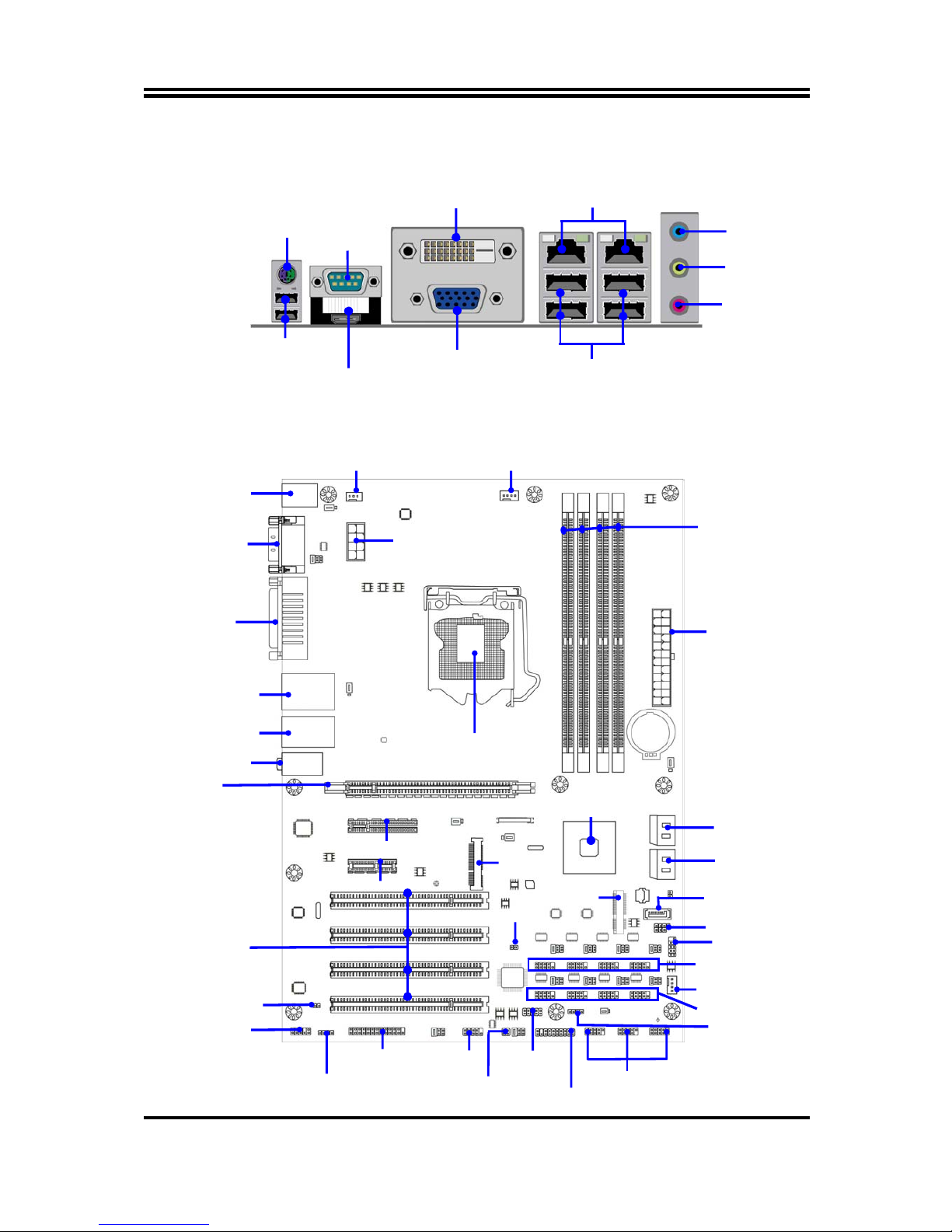
1-2 Layout Diagram
Rear IO Diagram
Motherboard Internal Diagram
RJ-45 LAN Ports
USB Ports
PS/2 KB/MS
Port
Line-IN/
Optical SPDIF OUT
Line-OUT
MIC-IN
USB Ports
Serial Port
VGA Port
ATX 12V Power
Connector
Front Panel Header
ATX Powe
r
Connector
CPU Socket LGA1155
Intel Q67
Chipset
Speaker /PWR LED Headers
DDRIII DIMMx4
32-bit PCI Slots
Serial Port over
HDMI port
Front Panel
Audio Heade
r
DVI port over
VGA Port
RJ-45 Over USB Ports
PCI Ex16 Slot
PS2 KB/MS Port
over
USB Ports
6-CH
Audio Connector
DVI Port
Parallel Header
TPM Header
HDMI S/PDIF Header
GPIO Heade
r
TX-RX COM
Header
MINI PCIE
Slot
PCIE x 4 Slots
SATA3_4 Connectors
CIR Heade
r
RJ-45 Over USB Ports
PCIE x1 Slot
CDIN Header
SYS FAN2
SATA1_2 Connectors
SATA5 Connecto
r
CASE OPEN
USB1, USB2, USB3 Headers
HDMI Port
MSATA
Connector
COM3/COM5/COM7/COM9
(from left to right)
COM4/COM6/COM8/COM10
COM 2
Page 7
3
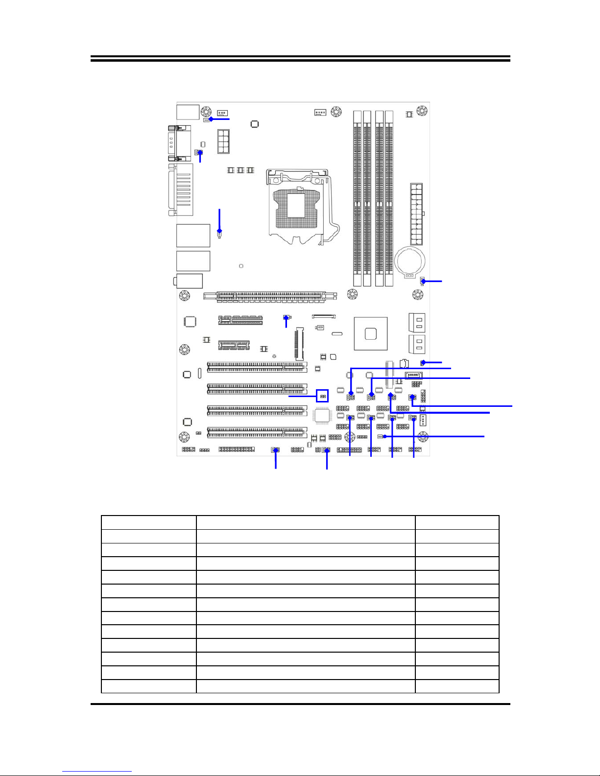
Motherboard Jumper Position
Jumper
Jumper Name Description
JBAT CMOS RAM Clear Function Setting 3-pin Block
JP3 USB Port Power On Function Setting 3-pin Block
JP5 USB Port Power On Function Setting 3-pin Block
JP8 COM2 Header Pin9 Function Selecting 6-pin Block
JP9 COM2 RS232/485/422 Function Selecting 6-pin Block
JP10 KB/MS/USB Power-On Function Setting 3-pin Block
JP11 COM2 Header Pin9 Function Selecting 6-pin Block
JP12 COM2 Header Pin9 Function Selecting 6-pin Block
JP13 COM2 Header Pin9 Function Selecting 6-pin Block
JP14 COM2 Header Pin9 Function Selecting 6-pin Block
JP15 COM2 Header Pin9 Function Selecting 6-pin Block
JP16 COM2 Header Pin9 Function Selecting 6-pin Block
JBAT
J
P10
JP5
J
P20
COPEN
J
P18
J
P13 JP15
JP9 J
P11
J
P19
J
P12
J
P2
JP
14
JP
16
JP
17
J
P8
JP
3
Page 8
4
JP17 COM2 Header Pin9 Function Selecting 6-pin Block
JP18 COM2 Header Pin9 Function Selecting 6-pin Block
JP19 COM2 Header Pin9 Function Selecting 6-pin Block
JP20 Mini PCI-E Power VCC3.3V/3.3V SB 3-pin Block
Connectors
Connector Name Description
KB/MS from UK1 PS2 Keyboard/Mouse Connector 6-pin Female
VGA1 Video Graphic Attach Connector 15-pin Female
DVI1 DVI Port Connector 24-pin Connector
USB from UL1/UL2 USB Port Connectors 4-pin Connectors
LAN from UL1/UL2 RJ-45 LAN Connectors 8-pin Connectors
COM1 Serial Port COM Connector 9-pin Connector
AUDIO Audio Connector 3-phone Jack
ATXPWR ATX Power Connector 24-pin Block
ATX12V1 ATX 12V Power Connector 8-pin Block
SATA3_4/SATA5 Serial ATAII Connectors 7-pin Connector
SATA1_2
Serial ATAⅢ Connector
7-pin Connector
USB from UK1 USB Port Connectors 4-pin Connectors
HDMI High-Definition Multimedia Interface 10-pin Connector
Headers
Header Name Description
FP_AUDIO Front panel audio Headers 9-pin block
CDIN CD Audio-In Header 4-pin Block
SPEAK Speaker Header 4-pin Block
PWRLED Power LED 3-pin Block
JW_FP
(Front Panel Header)
PWR LED/ HD LED/ /Power Button /Reset 9-pin Block
USB1 USB1 Header 9-pin Block
USB2 USB2 Header 9-pin Block
CPUFAN,SYSFAN2 FAN Speed Headers 4-pin Block
SYSFAN1 FAN Speed Header 3-pin Block
GPIO_CON GPIO Header 10-pin Block
COM2/3/4/5/6/7/8/9/10 Serial Port Headers 9-pin Block
TX-RXCOM1 RS 232/422/485 port headers 4-pin block
CIR CIR infrared module Headers 4-pin Block
HDMI_SPDIF SPDIF Out header 2-pin Block
TPM TPM Header 19-pin Block
USB3 USB Header 9-pin Block
CASE_OPEN Case Open Message Display Function 2-pin Block
Page 9
5
Chapter 2
Hardware Installation
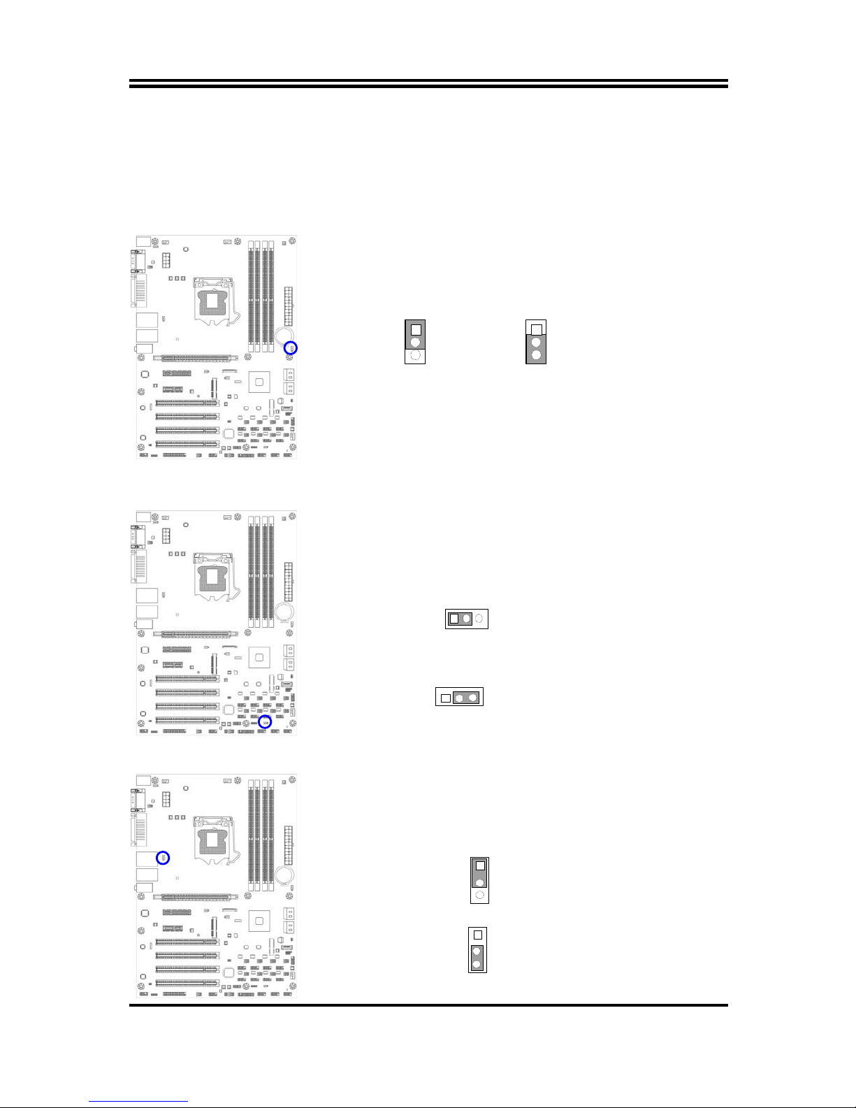
2-1 Jumper Setting
(1) Clear CMOS (3-pin): JBAT
1 1 1
3 3
CMOS Cl e ar Se tting
2-3 Short: Clear CMOS
JBAT
1-2 Sho r t: Normal
(2) JP3 (3-pin): USB Power On Function Setting
2-3 closed: USB POWER-O N Enabl ed
JP3
JP3
1-2 closed : USB POWER- O N Disabled(def ault)
1
3
1
3
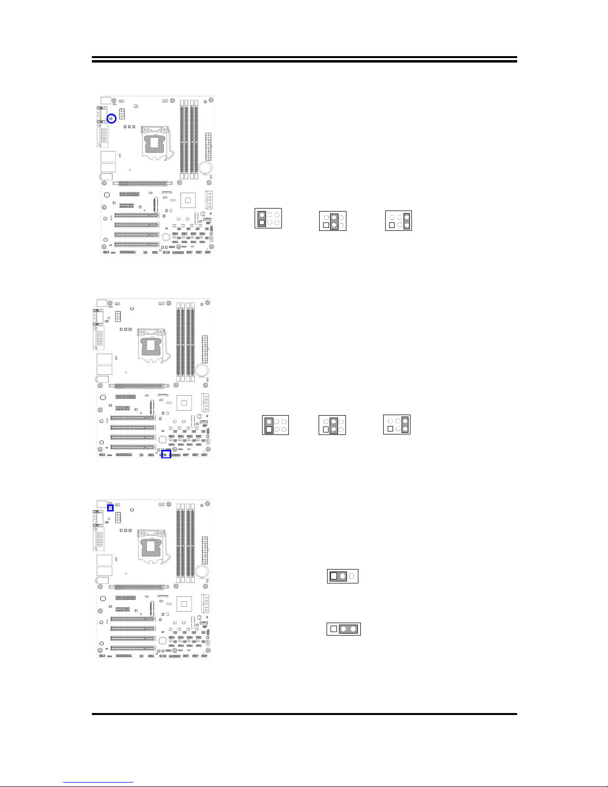
(3) JP5 (3-pin): USB Power On Function Setting
2-3 closed : USB POWER-ON En abled
JP5
JP5
1-2 closed : USB POWER-ON Disabled( default)
1
3
Page 10
6
(4) JP8 (6-pin): COM2 Header Pin9 Function Selecting
3-4 closed : +12V
JP8
1
1-2 closed: RS232
1
1
5-6 closed : +5V
(5) JP9 (6-pin): COM2 Port RS232/485/422 Function Select
3-4 closed : RS485
JP9
1-2 closed: RS232
5-6 closed : RS422
(6)JP10 (6-pin): KB/MS/USB Power-On Function Setting
2-3 closed: KB/MS/ USB POWER-ON Enabled
JP10
JP10
1-2 closed : KB/MS /U SB POWER-ON Disabled(default)
1
3
Page 11
7
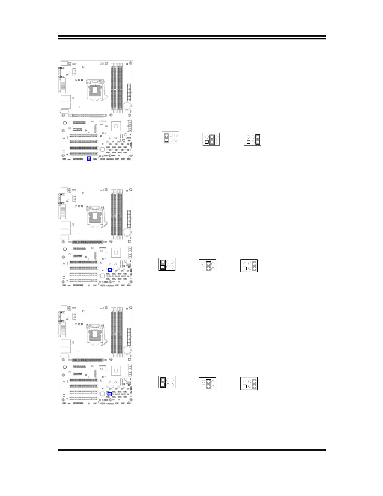
(7) JP11 (6-pin): COM2 Pin9 function select
3-4 closed : +12V
JP11
1
1-2 closed: RS232
1
1
5-6 closed : +5V
(8) JP12 (6-pin): COM3 Pin9 function select
3-4 closed : +12V
JP12
1
1-2 closed: RS232
1
1
5-6 closed : +5V
(9) JP13 (6-pin): COM4 Pin9 function select
3-4 closed : +12V
JP13
1
1-2 closed: RS232
1
1
5-6 closed : +5V
(10) JP14 (6-pin): COM5 Pin9 function select
Page 12
8
3-4 closed : +12V
JP14
1
1-2 closed: RS232
1
1
5-6 closed : +5V
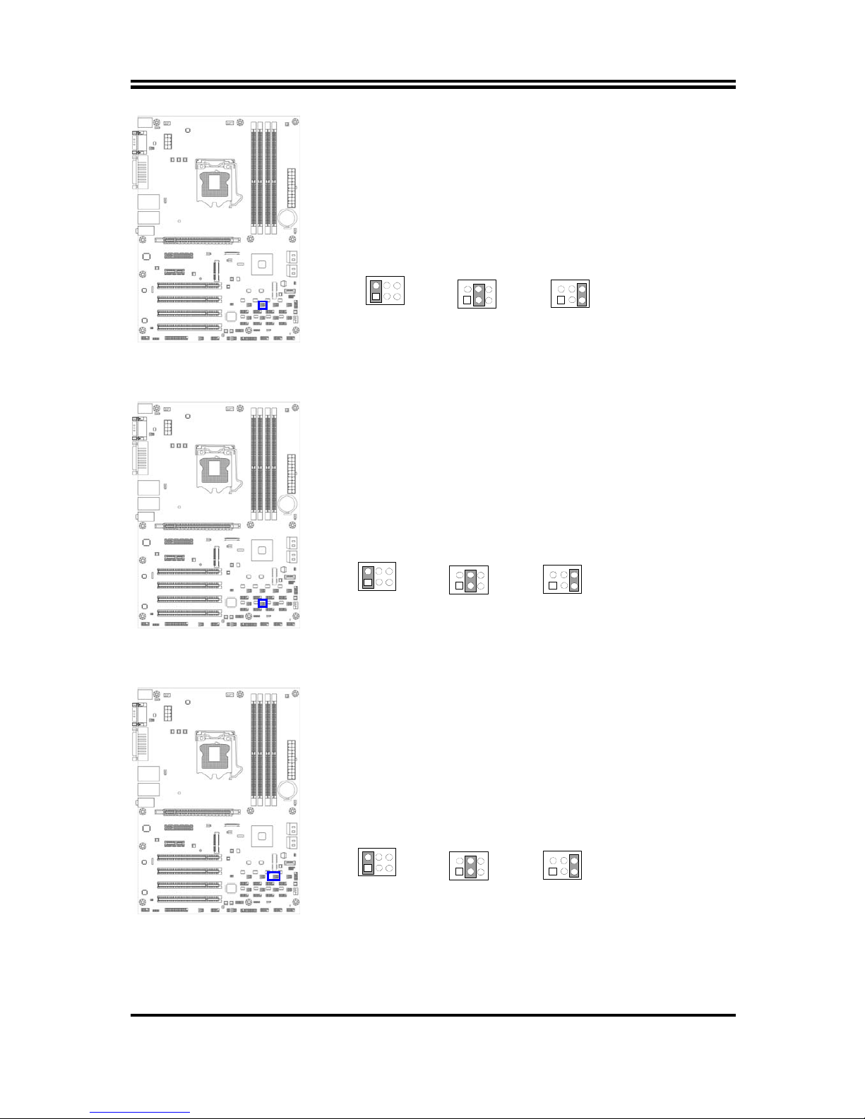
(11) JP15 (6-pin): COM6 Pin9 function select
3-4 closed : +12V
JP15
1
1-2 closed: RS232
1
1
5-6 closed : +5V
(12) JP16 (6-pin): COM7 Pin9 function select
3-4 closed : +12V
JP16
1
1-2 closed: RS232
1
1
5-6 closed : +5V
(13) JP17 (6-pin): COM9 Pin9 function select
Page 13

9
3-4 closed : +12V
JP17
1
1-2 closed: RS232
1
1
5-6 closed : +5V
(14)JP18 (6-pin): COM10 Pin9 function select
3-4 closed : +12V
JP18
1
1-2 closed: RS232
1
1
5-6 closed : +5V
(15)JP19 (6-pin): COM8 Pin9 function select
3-4 closed : +12V
JP19
1
1-2 closed: RS232
1
1
5-6 closed : +5V
Page 14
10
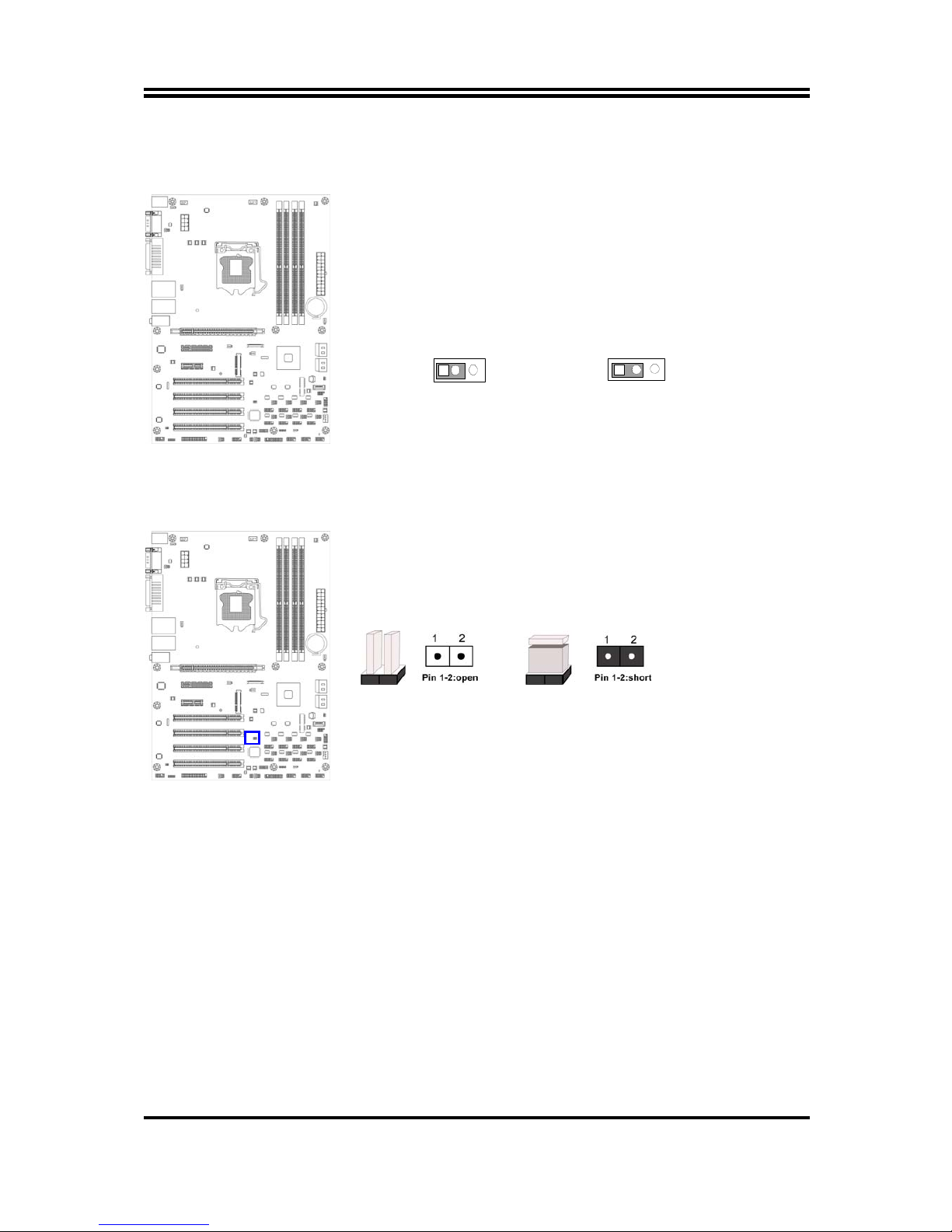
(16)JP20 (3-pin):
Mini PCI-E Power VCC 3.3V/3.3 VSB Function Select
2-3 cl osed : MINI PCI-E
VCC= 3.3VSB
JP20
1-2 closed : MINI PCI-E
VCC= 3. 3 V
31 3
1
(17) CASE_ OPEN (2-pin): Case Open Message Display function select
Case Open Display Function
1-2 Shor t : Case Open
CASE_OPEN
1-2 Open: Normal
Pin 1-2 shorted: Case open display function enabled. In this case if your case is
removed, next time when you restart your computer a message will be displayed
onscreen to inform you of this.
Page 15

11
2-2 Connectors and Headers
2-2-1 Rear I/O Back Panel Connectors
(1) PS/2 Keyboard Connector: UK1
The connectors are for PS/2 keyboard (Purple) and PS/2 Mouse (Green).
(2) D-Sub 15-pin Connector: VGA1
VGA connector is the 15-pin D-subminiature female connector; it is for the
display devices, such as the CRT monitor, LCD monitor and so on.
(3) Digital Visual Interface: DVI1
This interface standard designed to maximize the visual quality of digital display
devices such as flat panel LCD computer displays and digital projectors.
(4) USB Port connector: USB ports from UL1/ UL2/UK1
The connectors are 4-pin connector that connects USB devices to the system
board.
(5) LAN Port connectors: RJ45 LAN ports from UL1/UL2
The connector is standard RJ45 connector for Network. It supports
10/100/1000Mbps data transfer rate.
(6) Serial port connector: COM1
COM1 is a 9-pin serial port connector.
(7) Audio Line-In, Lin-Out connector: AUDIO
These Connectors are 3 Phone-Jack for LINE-OUT, LINE-IN, MIC audio
connections.
Line-in: (BLUE)
Audio input to sound chip
Line-out: (GREEN)
Audio output to speaker
MIC: (PINK)
Microphone Connector
USB Ports
PS/2 KB/MS Port
Line-IN/
Optical SPDIF OUT
Line-OUT
MIC-IN
USB Ports
Serial Port
VGA Port
DVI Port
RJ-45 LAN Port
HDMI Port
Page 16

12
2-2-2 Motherboard Internal Connectors
(1) Power Connector (24-pin block): ATXPWR
ATX Power Supply connector: This is a new defined 24-pins connector that
usually comes with ATX case. The ATX Power Supply allows using soft power
on momentary switch that connect from the front panel switch to 2-pins Power
On jumper pole on the motherboard. When the power switch on the back of the
ATX power supply turned on, the full power will not come into the system board
until the front panel switch is momentarily pressed. Press this switch again will
turn off the power to the system board.
** We recommend that you use an ATX 12V Specification 2.0-compliant power
supply unit (PSU) with a minimum of 350W power rating. This type has 24-pin
and 4-pin power plugs.
** If you intend to use a PSU with 20-pin and 4-pin power plugs, make sure that the
20-pin power plug can provide at least 15A on +12V and the power supply unit
has a minimum power rating of 350W. The system may become unstable or may
not boot up if the power is inadequate.
** If you are using a 20-pin power plug, please refer to Figure1 for power supply
connection. Power plug form power supply and power connectors from
motherboard both adopt key design to avoid mistake installation. You can insert
the power plug into the connector with ease only in the right direction. If the
direction is wrong it is hard to fit in and if you make the connection by force if is
possible.
Figure1:20-pin power plug Figure 2:24-pin power plug
Page 17

13
(2) ATX 12V Power Connector (8-pin block): ATX12V
This is a new defined 8-pin connector that usually comes with ATX Power
Supply. The ATX Power Supply which fully supports AMD AM3 processor must
including this connector for support extra 12V voltage to maintain system power
consumption. Without this connector might cause system unstable because the
power supply can not provide sufficient current for system.
Pin 1
(3) Serial-ATAII Port connector: SATA1_2/SATA3_4/SATA5
This connector supports the provided Serial ATA3 hard disk cable to connecting
the motherboard with SATA2 hard disk.
Pin No. Defnition
1 GND
2 TXP
3 TXN
4 GND
5 RXN
6 RXP
7 GND
Page 18

14
2-2-3 Header Pin Definition
(1) Line-Out/MIC Header for Front Panel (9-pin): FP_AUDIO
This header is connected to Front Panel Line-out, MIC connector with cable.
Line-Out, M IC Hea ders
Pin 1
Lineout2-L
Lineou t2-R
Sens e-FB
Audio-GND
LINE2- JD
Audio-JD
2
9
10
KEY
MIC2-L
MIC2-JD
MIC2-R
(2) CD AUDIO-In Headers (4-pin): CDIN
CDIN are the connectors for CD-Audio Input signal. Please connect it to
CD-ROM CD-Audio output connector.
CD Au dio-In Headers
CDIN
1 4
GNDCD-L
CD-RGND
3) Speaker connector: SPEAK
This 4-pin header connects to the case-mounted speaker. See the figure below.
(4) Power LED: PWR LED
The Power LED header is light on while the system power is on. Connect the
Power LED header from the system case to this pin.
Page 19

15
SPEAK1
SPEAK
NC
NC
VCC
Pin 1
PWRLED1
Pin 1
VCC
GND
GND
(5) Front Panel Header: JW-FP
HDLED
RESET
VCC5
GND
VCC5
PWR LED
PWRBTN
PWRBTN
PWRLED
HDDLE
RSTSW
NC
GND
JW FP
Pin 1
(6) USB Port Headers (4-pin): USB1/USB2/USB3
Pin 1
USB1
VCC
-DAT A
GND
+DATA
VCC
O
C
-DATA
GND
+DATA
Page 20

16
(7) FAN Power Headers: SYSFAN1 (3-pin); SYSFAN2 (4-pin); CPUFAN (4-pin)
DE
T
VCC
4
1
GND
FAN Headers
SYSFAN1
1
4
CPUFAN
Control
GND
GND
V
CC
Control
DET
Fan
Clock
SYSFAN2
1
+12V
(8) GPIO Header (10-pin): GPIO_CON
GPIO_ CON He ader
9
GPIO_30
GND
GPIO_32
GPIO_34
GPIO_36
GPIO_31
GPIO_35
GPIO 33
2
Pin 1
10
GPIO_37
VCC
(9) Serial Port Header (9-Pin): COM2/3/4/5/6/7/8/9/10
Serial COM Port 9-pin B lock
Pin1
Pin
6
DCD
Pin5
DSR
RXD
TXD
DTR
GND
RTS
CTS
RI
Page 21

17
(10) RS232/422/485 Header (4-pin): TX-RXCOM1
TX-RX Header
TX-RXCOM1
Pin 1
RXDP
TXDN
TXDP
3
RXDN
2
4
(11) HDMI-SPDIF Out header (2-pin): HDMI_SPDIF
HDMI_SPDIF Header
1
GND
2
HDMI_SPDIF_OUT
(12) TPM Header (19-pin):TPM
TPM Head e r
19
CLK
VCC3.3V
LFRAME-
RESET
LAD3
GND
VCC5V
KEY/NC
2
Pin 1
20
LAD2
LAD1
LAD0
GPIO
SB3.3V
GND
GN
D
GPIO
SERIRQ
NC/GND
GPIO
GPIO
Page 22

18
Chapter 3
Introducing BIOS
Notice!
The BIOS options in this manual are for reference only. Different
configurations may lead to difference in BIOS screen and BIOS
screens in manuals are usually the first BIOS version when the board
is released and may be different from your purchased motherboard.
Users are welcome to download the latest BIOS version form our
official website.
The BIOS is a program located on a Flash Memory on the motherboard. This program
is a bridge between motherboard and operating system. When you start the computer,
the BIOS program will gain control. The BIOS first operates an auto-diagnostic test
called POST (power on self test) for all the necessary hardware, it detects the entire
hardware device and configures the parameters of the hardware synchronization.
Only when these tasks are completed done it gives up control of the computer to
operating system (OS). Since the BIOS is the only channel for hardware and software
to communicate, it is the key factor for system stability, and in ensuring that your
system performance as its best.
3-1 Entering Setup
Power on the computer and by pressing <Del> immediately allows you to enter Setup.
If the message disappears before your respond and you still wish to enter Setup,
restart the system to try again by turning it OFF then ON or pressing the “RESET”
button on the system case. You may also restart by simultaneously pressing <Ctrl>,
<Alt> and <Delete> keys. If you do not press the keys at the correct time and the
system does not boot, an error message will be displayed and you will again be asked
to
Press
<Del>
to enter Setup
Page 23

19
3-2 BIOS Menu Screen
The following diagram show a general BIOS menu screen:
BIOS Menu Screen
3-3 Function Key
In the above BIOS Setup main menu of, you can see several options. We will explain
these options step by step in the following pages of this chapter, but let us first see a
short description of the function keys you may use here:
z
Press←→ (left, right) to select screen;
z
Press ↑↓ (up, down) to choose, in the main menu, the option you want to confirm
or to modify.
z
Press <Enter> to select.
z
Press <+>/<–> keys when you want to modify the BIOS parameters for the active
option.
z
[F1]: General help.
z
[F2]: Previous value.
z
[F3]: Optimized defaults.
z
[F4]: Save.
z
Press <Esc> to quit the BIOS Setup.
Menu Bar
Menu Items
Current Setting Value
Function Keys
General Help Items
Page 24

20
3-4 Getting Help
Main Menu
The on-line description of the highlighted setup function is displayed at the top right
corner the screen.
Status Page Setup Menu/Option Page Setup Menu
Press F1 to pop up a small help window that describes the appropriate keys to use
and the possible selections for the highlighted item. To exit the Help Window, press
<
Esc
>.
3-5 Menu Bar
There are six menu bars on top of BIOS screen:
Main To change system basic configuration
Advanced To change system advanced configuration
Chipset To change chipset configuration
Boot To change boot settings
Security Password settings
Save & Exit Save setting, loading and exit options.
User can press the right or left arrow key on the keyboard to switch from menu bar.
The selected one is highlighted.
Page 25

21
3-6 Main Menu
Main menu screen includes some basic system information. Highlight the item and
then use the <+> or <-> and numerical keyboard keys to select the value you want in
each item.
System Date
Set the date. Please use TAB to switch between data elements.
System Time
Set the time. Please use TAB to switch between time elements.
Page 26

22
3-7 Advanced Menu
Page 27

23
Launch LAN1/LAN2 PXE OpROM
Use this item to enable or disable boot option for legacy network devices.
Launch Storage OpROM
Use this item to enable or disable boot option for legacy mass storage devices with
option ROM.
ERP Function
Use this item to enable or disable ERP function for this board.
► PCI Subsystem Settings
Press [Enter] to enter and make settings for the following sub-items:
PCI ROM Priority
The optional settings: [Legacy ROM]; [EFI Compatible ROM].
PCI Latency Timer
Use this item to select value to be programmed into PCI Latency Timer Register.
The optional settings: 32/64/96/128/160/192/224/248 PCI Bus Clocks.
VGA Palette Snoop
Use this item to enable or disable VGA Palette Registers Snoop.
PERR# Generation
Use this item to enable or disable PCI Device to Generate PERR#.
SERR# Generation
Use this item to enable or disable PCI Device to Generate SERR#.
Relaxed Ordering
Use this item to enable or disable PCI express device relaxed ordering.
Extended Tag
If set as [Enabled] it will allow device to use 8-bit tag filed as a requester.
No Snoop
Use this item to enable or disable PCI Express device No Snoop option.
Maximum Payload
Use this item to set maximum payload of PCI Express device or allow system
BIOS to select the value.
Maximum Read Request
Use this item to set maximum read request size of PCI Express device or allow
system BIOS to select the value.
ASPM Support
The optional settings: [Disabled]; [Auto];[Force L0].
Extended Synch
If set as [Enabled] it will allow generation of extended synchronization patterns.
► ACPI Settings
ACPI Sleep State
Use this item to select the highest ACPI sleep state the system will enter when the
suspend button is pressed.
Page 28

24
► Wakeup Function settings
Wake System with Fixed Time
Use this item to enable or disable system wake on alarm event. When set as
Enabled, system will wake on the hour/min/sec specified.
Wake System with Dynamic Time
Use this item to enable or disable system wake on alarm event. When set as
[Enabled], system will wake on the current plus increased minute(s).
CIR Wakeup
Use this item to enable or disable CIR wakeup.
PS2 KB/MS Wakeup
Use this item to enable or disable PS2 KB/MS wakeup function.
PCI PME Wakeup
Use this item to enable or disable S3/S4/S5 PCI PME Wakeup function, Support
Only Disable EUP.
► Trusted Computing
Use this item to enable or disable TPM support. O.S. will not show TPM. Reset of
platform is required
► CPU Configuration
Socket 0 CPU Information
Use this item to view the Socket specific CPU Information.
Active Processor Cores
Use this item to select number of cores to enable in each processor package.
Limit CPUIO Maximum
This item should be set as [Disabled] for Windows XP.
Execute Disable Bit
XD can prevent certain classes of malicious buffer overflow attacks when
combined with a supporting OS (Windows Server 2003 SP1, Windows XP SP2,
SuSe Linux 9.2, RedHat Enterprise 3 Update 3.)
Hardware Prefetcher
Use this item to turn on/off the MLC (L2) streamer prefetcher.
Adjacent Cache Line Prefetch
Use this item to turn on/off prefetching of adjacent cache lines.
Intel Virtualization Technology
The optional settings: [Enabled]; [Disabled].
When set as [Enabled], a VHM can utilize the additional hareware capabilities
provided by Vanderpool Technology.
Power Technology
Use this item to enable power management features.
The optional settings are: [Disabled]; [Energy Efficient]; [Custom].
Page 29

25
► SATA Configuration
SATA Mode
The optional settings are: [Disabled]; [IDE Mode]; [AHCI Mode]; [RAID Mode].
Serial-ATA Controller 0
The optional settings are: [Disabled]; [Enhanced]; [Compatible].
Serial-ATA Controller 1
The optional settings are: [Disabled]; [Enhanced].
► Intel IGD SWSCI OpRegion
IGD-Boot Type
Use this item to select the video device which will be activated during POST. This
has no effect if external graphics present.
Active LFP
Use this item to select the Active LFP Configuration.
LCD Panel Type
Use this item to select the LCD panel used by internal graphics device.
► USB Configuration
Legacy USB Support
The optional settings are: [Auto];[Disabled]; [Enabled].
EHCI Hand-off
The optional settings are: [Disabled]; [Enabled].
USB Transfer time-out
Use this item to set the time-out value for control, bulk, and interrupt transfers.
Device reset time-out
Use this item to set USB mass storage device start unit command time-out.
Device power-up delay
Use this item to set maximum time the device will take before it properly reports
itself to the host controller. ‘Auto’ uses default value: for a root port it is 100 ms, for
a hub port the delay is taken from hub descriptor.
► Super I/O Configuration
Press [Enter] to enter into the sub-item.
► COM1 Port Configuration
Serial Port
Use this item to enable or disable serial port (COM).
Change Settings
Use this item to select an optimal setting for super IO device.
Page 30

26
► COM2 Port Configuration
Serial Port
Use this item to enable or disable serial port (COM).
Change Settings
Use this item to select an optimal setting for super IO device.
Serial Port Mode Select
Use this item to set serial port as RS232 or RS422/485.
CIR Controller
Use this item to enable or disable CIR controller.
► Parallel Port Configuration
Parallel port
Use this item to enable or disable Parallel port (LPT/LPTE)
Change Settings
Use this item to select an optimal setting for super IO device.
Device Mode
Use this item to change the Printer Port.
PS2 KB/MS Connect
Use this item to setting PS2 Connect Primary Devices.
The optional settings are:[Keyboard First], [Mouse First]
CIR Controller
Use this item to enable or disable CIR controller.
Case Open Detect
Use this item to detect whether Case has already opened or not. Show message
in POST.
► PC Health Monitor
Press [enter] to view hardware health status.
► Second Super IO Configuration
COM3/COM4/ COM5/COM6 Configuration
Serial Port
Use this item to enable or Disable serial port (COM1).
Change Settings
Use this item to select an optimal setting for super IO device.
► Third Super IO Configuration
COM7/COM8/COM9/COM10 Configuration
Serial Port
Use this item to enable or Disable serial port (COM1).
Change Settings
Use this item to select an optimal setting for super IO device.
► AMT Configuration
The optional settings: [Enabled]; [Disabled].
Unconfigure AMT/ME
Use this item to perform AMT/ME unconfigure without password operation.
Page 31

27
► Voltage Configuration
CPU Vcore 7-Shift
Use this item to adjust CPU voltage by 7 step value.
AXG Voltage
Use this item to adjust AGX voltage by 7 step value.
CPU VTT
Use this item to adjust CPU VTT voltage by 7 step value.
► WatchDog Configuration
WatchDog Timer Control
Use this item to enable or disable WatchDog Timer Control. When set as Enabled,
the following sub-items shall appear:
WatchDog Timer Value
User can set a value in the range of 4 to 255.
WatchDog Timer Unit
The optional settings are: [Second]; [Minute].
► Chipset Voltage Configuration
Use this item to choose the Voltage Parameters.
► Shutdown Temperature Configuration
Use this item to select system shutdown temperature.
► Serial Port Console Redirection
Console Redirection
The optional settings: [Enabled]; [Disabled].
► SmartFan Configuration
CPU FAN Smartfan Mode
Use this item to enable or disable Smartfan Mode.
3/4 Pin Fan Select
The optional settings are: [3 pin]/ [4 pin Fan].
SYSFAN1 Smart Mode
Use this item to enable or disable Smartfan Mode.
SYSFAN2 Smart Mode
Use this item to enable or disable Smartfan Mode.
Page 32

28
3-8 Chipset Menu
► North Bridge
LOW MMIO Align
The optional settings are: [64M]; [1024M].
VT-d
Use this item to enable or disable VT-d
Initiate Graphics Adapter
Select which graphics controller to use as the primary boot device.
The optional settings are: [IGD]; [PCI/IGD]; [PCI/PEG]; [PEG/IGD]; [PEG/PCI].
IGD Memory
Use this item to select IGO Share Memory Size
The optional settings are: [Disable]/[32m]/[64m]/[128m]/[256m]/[512m].
IGD Multi-Monitor
Use this item to enable or disable IGD Multi-Monitor by Internal Graphics Device.
PCI Express Port
The optional settings are: [Disabled]/[Enabled]/[Auto].
PEG Force Gen1
The optional settings are: Enabled]; [Disabled].
Detect Non- Compliance Device
Use this item to detect Non- Compliance PCI Express Device in PEG.
Page 33

29
► South Bridge
Wake on Lan from S5
Use this item to enable or disable GbE control PME in S5.
Onboard Lan1 Device
Use this item to enable or disable the PCI Express Ports in the Chipset.
Restore AC Power Loss
Use this item to specify what state to go to when power is re-applied after a power
failure (G3 State). The optional settings are: [Power Off]; [Power On]; [Last State].
SLP_S4 Assertion Stretch Enable
The optional settings are: [Enabled]; [Disabled].
Deep SX
Deep SX Configuration
NOTE: Mobile platforms support Deep S4/S5 in DC only and Desktop platforms
support Deep S4/S5 in AC only.
Azalia HD Audio
The optional settings are: [Enabled]; [Disabled].
Azalia Internal HDMI Codec
Use this item to enable or disable internal HDMI codec for Azalia.
High Precision Timer
The optional settings are: [Enabled]; [Disabled].
► USB Configuration
Press [Enter] to further setting USB port configuration.
► ME subsystem
ME Subsystem
Use this item to enable or disable ME subsystem help.
ME Temporary Disable
The optional settings are: [Enabled]; [Disabled].
End of Post Message
The optional settings are: [Enabled]; [Disabled].
Execute MEBX
The optional settings are: [Enabled]; [Disabled].
MEBX Mode
The optional settings are:[normal]/[Hidden Ctrl+p]/Enter MEBX Setup.
Page 34

30
3-9 Boot Menu
Setup Prompt Timeout
Use this item to set number of seconds to wait for setup activation key.
Bootup Numlock State
Use this item to select keyboard numlock state. The optional settings are: [On]; [Off].
Quite Boot
Use this item to enable or disable Quite Boot option.
Gate A20 Active
The optional settings are: [Upon Request]; [Always].
Option ROM Message
Use this item to set display mode for option ROM. The optional settings are: [Force
BIOS]; [Keep Current].
Interrupt 19 Capture
The optional settings are: [Enabled]; [Disabled].
Page 35

31
3-10 Security Menu
Security menu allow users to change administrator password and user password
settings.
Page 36

32
3-11 Save & Exit Menu
Save & Exit menu allows user to load optimal defaults, save or discard your changes
to BIOS items.
 Loading...