

Page 1

Intel® PXA27x Processor Family
Design Guide
May 2005
Order No. 280001-002
Page 2

Contents
INFORMATION IN THIS DOCUMENT IS PROVIDED IN CONNECTION WITH INTEL PRODUCTS. NO LICENSE, EXPRESS OR IMPLIED BY
ESTOPPEL OR OTHERWISE, TO ANY INTELLECTUAL PROPERTY IS GRANTED BY THIS DOCUMENT. EXCEPT AS PROVIDED IN INTEL’S
TERMS AND CONDITIONS OF SALE FOR SUCH PRODUCTS, INTEL ASSUMES NO LIABILITY WHATSOEVER, AND INTEL DISCLAIMS ANY
EXPRESS OR IMPLIED WARRANTY RELATING TO SALE AND/OR USE OF INTEL PRODUCTS, INCLUDING LIABILITY OR WARRANTIES
RELATING T O FITNESS FOR A PARTICULAR PURPOSE, MERCH ANTABILITY, OR INFRINGEMENT OF ANY PATENT , COPYRIGHT, OR OTHER
INTELLECTUAL PROPERTY RIGHT.
Intel Corporation may have patents or pending patent applications, trademarks, copyrights, or other intellectual property rights that relate to the
presented subject matter. The furnishing of documents and other materials and information does not provide any license, express or implied, by
estoppel or otherwise, to any such patents, trademarks, copyrights, or other intellectual property rights.
Intel products are not intended for use in medical, life saving, life sustaining, critical control or safety systems, or in nuclear facili ty appl ica tions.
Intel may make changes to specifications and product descriptions at any time, without notice.
Designers must not rely on the absence or characteristics of any features or instructions marked “reserved” or “undefined.” Intel reserves these for
future definition and shall have no responsibility whatsoever for conflicts or incompatibilities arising from future changes to them.
®
The Intel
specifications. Current characterized errata are available on request.
MPEG is an international standard for video compression/decompression promoted by ISO. Implementations of MPEG CODECs, or MPEG enabled
platforms may require licenses from various entities, including Intel Corporation.
This document and the software described in it are furnished under license and may only be used or copied in accordance with the terms of the
license. The information in this document is furnished for informational use only, is subject to change without notice, and should not be construed as a
commitment by Intel Corporation. Intel Corporation assumes no responsibility or liability for any errors or inaccuracies that may appear in this
document or any software that may be provided in association with this document. Except as permitted by such license, no part of this document may
be reproduced, stored in a retrieval system, or transmitted in any form or by any means without the express written consent of Intel Corporation.
Contact the local Intel sales office or the distributor to obtain the latest specifications and before placing the product order.
Copies of documents which have an ordering number and are referenced in this document, or other Intel literature may be obtained by calling
1-800-548-4725 or by visiting Intel's website at http://www.intel.com.
Copyright © Intel Corporation, 2005
AlertVIEW, i960, AnyPoint, AppChoice, BoardWatch, BunnyPeople, CablePort, Celeron, Chips, Commerce Cart, CT Connect, CT Media, Dialogic,
DM3, EtherExpress, ETOX, FlashFile, GatherRound, i386, i486, iCat, iCOMP, Insight960, InstantIP, Intel, Intel logo, Intel386, Intel486, Intel740,
IntelDX2, IntelDX4, IntelSX2, Intel ChatPad, Intel Create&Share, Intel Dot.Station, Intel GigaBlade, Intel InBusiness, Intel Inside, Intel Inside logo, Intel
NetBurst, Intel NetStructure, Intel Play, Intel Play logo, Intel Pocket Concert, Intel Quick Capture T echnology , Intel SingleDriver, Intel SpeedStep, Intel
StrataFlash, Intel TeamStation, Intel WebOutfitter, Intel Xeon, Intel XScale, Itanium, JobAnalyst, LANDesk, LanRover, MCS, MMX, MMX logo,
NetPort, NetportExpress, Optimizer logo, OverDrive, Paragon, PC Dads, PC Parents, Pentium, Pentium II Xeon, Pentium III Xeon, Performance at
Your Command, ProShare, Quick Capture Technology , RemoteExpress, Screamline, Shiva, SmartDie, Solutions960, Sound Mark, StorageExpress,
The Computer Inside, The Journey Inside, This Way In, TokenExpress, Trillium, Vivonic, VTune, and Wireless Intel SpeedStep Technology are
trademarks or registered trademarks of Intel Corporation or its subsidiaries in the United States and other countries.
*Other names and brands may be claimed as the property of others.
PXA27x Processor Family may contain design defects or errors known as errata which may cause the product to deviate from published
ii Intel® PXA27x Processor Family Design Guide
Page 3

Contents
Contents
Part I
1 Introduction to Part I ...............................................................................................................I: 1-1
1.1 Document Organization and Overview...........................................................................I: 1-1
1.2 Functional Ov erv ie w ............ .... .... .... ... .... .... .... .... .... ... .... .... .... .... .... ... .... .... .... .... ... .... .... ...I: 1-2
1.3 Package Introduction......................................................................................................I: 1-3
1.4 Signal Pin Descriptions...................................................................................................I: 1-4
2 PCB Design Guidelines...........................................................................................................I: 2-1
2.1 Intel
2.2 General PCB Ch ar ac ter ist ics.................. .... .... .... .... ... .... .... .... .... .... ... .... .... .... .... ... .... .... ...I: 2-1
2.3 Power Supply Decoupling Requirements .....................................................................I: 2-12
2.4 Thermal Cons ide ra tio ns....... .... .... .... ... .... .... .... .... .... ... .... .... .... .... .... ... .... .... .... .... ... .... .... .I: 2-12
2.5 Package to Board Assembly Process...........................................................................I: 2-12
2.6 Silicon Daisy Chain (SDC) Evaluation Units.................................................................I: 2-12
2.7 Handling: Shipping Media.............................................................................................I: 2-12
2.8 Preconditioning and Moisture Sensitivity......................................................................I: 2-13
2.9 Tray Specifications .......................................................................................................I: 2-13
®
Flash Memory Design Guidelines .........................................................................I: 2-1
2.2.1 PCB Layer Assignment (Stackup) .....................................................................I: 2-2
2.2.2 PCB Compone nt Pl ace m en t.................. .... ... .... .... .... .... .... ... .... .... .... .... ... .... .... ...I: 2-4
2.2.3 PCB Escape Routing.........................................................................................I: 2-7
2.2.3.1 VF-BGA Escape Routing ...................................................................I: 2-8
2.2.3.2 FS-CSP Escape Routing ...................................................................I: 2-9
2.2.3.3 PBGA Escape Rout ing............... ... .... ....................... .... .... .... ... .........I: 2- 10
2.2.4 PCB Keep-out Zo ne s................. .... .... .... .... ... .... .... .... .... .... ... .... .... .... .... ... .... .... .I: 2-11
2.2.5 Recommended Mobile Handset Dimensions...................................................I: 2-11
3 Design Chec k Lis t ...................................................................................................................I: 3-1
4 Mixed Voltage Design Considerations ..................................................................................I: 4-1
4.1 Overview.........................................................................................................................I: 4-1
4.2 Required Power Supplies ...............................................................................................I: 4-1
4.3 Example Power Supply Utilizing Minimal Regulators .....................................................I: 4-2
4.4 Cautions..........................................................................................................................I: 4-4
5 Power Measurements..............................................................................................................I: 5-1
5.1 Overview.........................................................................................................................I: 5-1
5.2 Measurement Guidelines................................................................................................I: 5-1
5.2.1 Measure Voltage Across a Series Resistor .......................................................I: 5-1
5.2.2 Measure Current Directly with a Current Meter in Series ..................................I: 5-1
5.3 Achieve Minimum Power Usage During All Power Modes .............................................I: 5-2
5.4 Achieve Minimum Power Usage During Deep Sleep .....................................................I: 5-2
5.5 Achieve Minimum Power Usage During Sleep...............................................................I: 5-3
5.6 Achieve Minimum Power Usage During Standby ...........................................................I: 5-3
5.7 Achieve Minimum Power Usage During Idle/13M/Run/Turbo ........................................I: 5-3
Intel® PXA27x Processor Family Desig n Guide iii
Page 4

Contents
Part II
1 Introduction to Part II .............................................................................................................II: 1-1
2 Package and Pins...................................................................................................................II: 2-1
3 Clocks and Power Interface...................................................................................................II: 3-1
3.1 Overview........................................................................................................................II: 3-1
3.2 Signals...........................................................................................................................II: 3-1
3.2.1 Clock Interfac e Sig na ls............. .... .... .... .... .... ... .... .... .... .... .... ... .... .... .... .... ... .... ...II: 3-1
3.2.2 Power Manager Interface Control Signals........................................................II: 3-2
3.2.3 Power Enable (PWR_EN).................................................................................II: 3-3
3.2.3.1 System Power Enable (SYS_EN).....................................................II: 3-3
3.2.3.2 Power Manager I2C Clock (PWR_SCL) ...........................................II: 3-3
3.2.3.3 Power Manager I2C Data (PWR_SDA) ............................................II: 3-3
3.2.3.4 nVDD_FAULT...................................................................................II: 3-3
3.2.3.5 nBATT_FAULT .................................................................................II: 3-4
3.3 Block Diagram ...............................................................................................................II: 3-4
3.4 Layout Notes..................................................................................................................II: 3-6
3.5 Modes of Ope rat ion s .......... .... .... .... .... ... .... .... .... .... .... ... .... .... .... .... .... ... .... .... .... .... ... .... ...II: 3-6
3.5.1 Clock Interfac e.... ... .... .... .... .... ... .... .... .... .... .... ... .... .... .... .... .... ... .... .... .... .... ... .... ...II: 3-6
3.5.1.1 Using the On-Chip Oscillator with a 32.768-KHz Crystal..................II: 3-7
3.5.1.2 Using an External 32.768- KH z Clo ck............... .... ... .... .... .... .... ... .... ...II: 3-7
3.5.1.3 Using the On-Chip Oscillator with a 13.000-MHz Crystal .................II: 3-7
3.5.1.4 Using an External 13.00-MHz Clock.................................................II: 3-8
3.5.2 Power Interface.................................................................................................II: 3-8
3.5.2.1 Power Supplies.................................................................................II: 3-8
4Internal SRAM.........................................................................................................................II: 4-1
4.1 Overview........................................................................................................................II: 4-1
4.2 Signals...........................................................................................................................II: 4-1
4.3 Block Diagram ...............................................................................................................II: 4-1
4.4 Layout Notes..................................................................................................................II: 4-2
5 DMA Controller Interface .......................................................................................................II: 5-1
5.1 Overview........................................................................................................................II: 5-1
5.2 Signals...........................................................................................................................II: 5-1
5.3 Block Diagram ...............................................................................................................II: 5-2
5.4 Layout Notes..................................................................................................................II: 5-2
5.5 Modes of Ope rat ion .................... .... .... ... .... .... .... .... .... ... .... .... .... .... .... ... .... .... .... .... ... .... ...II: 5-3
5.5.1 Fly-By DMA Transfers ......................................................................................II: 5-3
5.5.1.1 Signals..............................................................................................II: 5-3
5.5.1.2 Block Diagram........ ... .... .... .... .... .... ... .... .... .... .... .... ... .... .... .... .... ... .... ...II: 5-4
5.5.1.3 Layout Notes.....................................................................................II: 5-4
5.5.2 Flow-Through DMA Transfers ..........................................................................II: 5-5
5.5.2.1 Signals..............................................................................................II: 5-5
5.5.2.2 Block Diagram........ ... .... .... .... .... .... ... .... .... .... .... .... ... .... .... .... .... ... .... ...II: 5-5
5.5.2.3 Layout Notes.....................................................................................II: 5-6
6 System Memory Interface......................................................................................................II: 6-1
6.1 Overview........................................................................................................................II: 6-1
6.2 Signals...........................................................................................................................II: 6-3
iv Intel® PXA27x Processor Family Design Guide
Page 5

Contents
6.3 Block Diagram ......................... .... .... ... .... .... .... .... .... ... .... .... .... .... .... ... .... .... .... .... ... .... .... ..II: 6-5
6.4 Memory Contr oll er La yo ut No te s . .... ... .... .... .... .... .... ... .... .... .... .... .... ... .... .... .... .... ... .... .... ..II: 6-6
6.4.1 Memory Controller Routing Guidelines for 0.5mm and 0.65 mm Ball Pitch......II: 6-6
6.4.1.1 System Bus Recommended Signal Routing Guidelines
(Excluding SDCLK<x> and SDCAS).................................................................II: 6-6
6.4.1.2 SDCLK and SDCAS Recommended Signal Routing Guidelines......II: 6-7
6.4.1.3 Minimum Board Stack-up Configuration used for Signal Integrity ....II: 6-8
6.5 Modes of Operation Overview .......................................................................................II: 6-9
6.5.1 SDRAM Interface..............................................................................................II: 6-9
6.5.1.1 SDRAM Signals ................................................................................II: 6-9
6.5.1.2 SDRAM Memory Block Diagram.....................................................II: 6-11
6.5.1.3 SDRAM Layout Notes.....................................................................II: 6-12
6.5.2 Flash Memory Interface (Asynchronous/Synchronous)..................................II: 6-15
6.5.2.1 Flash Memory Signals ....................................................................II: 6-15
6.5.2.2 Flash Block Diagram.......................................................................II: 6-16
6.5.2.3 Flash Layout Note...........................................................................II: 6-16
6.5.3 ROM Interface ................................................................................................II: 6-17
6.5.3.1 ROM Signals...................................................................................II: 6-17
6.5.3.2 ROM Block Diagram .......................................................................II: 6-18
6.5.3.3 ROM Layout Notes .........................................................................II: 6-18
6.5.4 SRAM Interface ..............................................................................................II: 6-18
6.5.4.1 SRAM Signals.................................................................................II: 6-19
6.5.4.2 SRAM Block Diagram ................ ... .... .... .... .... .... ... .... .... .... .... ... .... ....II: 6-20
6.5.4.3 SRAM Layout Notes .......................................................................II: 6-20
6.5.5 Variable Latency Input/Output (VLIO) Interface..............................................II: 6-21
6.5.5.1 VLIO Memory Signals.....................................................................II: 6-22
6.5.5.2 VLIO Block Diagram .......................................................................II: 6-23
6.5.5.3 VLIO Memory Layout Notes............................................................II: 6-23
6.5.6 PC Card (PCMCIA) Interface..........................................................................II: 6-23
6.5.6.1 PC Card Signals .............................................................................II: 6-25
6.5.6.2 PC-Card Block Diagr am s...................... .... .... .... ... .... .... .... .... ... .... ....II: 6-26
6.5.6.3 PC Card Layout Notes....................................................................II: 6-29
6.5.7 Alternate Bus Master Interface .......................................................................II: 6-29
6.5.7.1 Alternate Bus Master Signals..........................................................II: 6-31
6.5.7.2 Alternate Bus Master Block Diagram..............................................II: 6-32
6.5.7.3 Alternate Bus Master Layout Notes ................................................II: 6-32
7LCD Interface..........................................................................................................................II: 7-1
7.1 Overview........................................................................................................................II: 7-1
7.2 Signals...........................................................................................................................II: 7-2
7.3 Schematics/Block Diagram............................................................................................II: 7-3
7.4 Layout Notes..................................................................................................................II: 7-3
7.4.1 Contrast Voltage...............................................................................................II: 7-3
7.4.2 Backlight Inver ter ........................... .... .... .... ... .... .... .... .... .... ... .... .... .... .... ... .... .... ..II: 7-4
7.4.3 Signal Routing and Buffering............................................................................II: 7-4
7.4.4 Panel Connector...............................................................................................II: 7-5
7.5 Modes of Operation Overview .......................................................................................II: 7-6
7.5.1 Passive Monoc hr om e Sin gl e-S ca n Mo d e............. .... .... .... ... .... .... .... .... ... .... .... ..II: 7-6
7.5.1.1 Signals ..............................................................................................II: 7-6
7.5.1.2 Schematics/Block Diagram...............................................................II: 7-7
7.5.1.3 Layout Notes....... ... ....................... .... .... .... .... ....................... ... .... .... ..II: 7-7
7.5.2 Passive Monochrome Single-Scan Double-Pixel Mode....................................II: 7-8
Intel® PXA27x Processor Family Design Guide v
Page 6

Contents
7.5.2.1 Signals..............................................................................................II: 7-8
7.5.2.2 Schematics / Block Diagram.............................................................II: 7-9
7.5.2.3 Layout Notes.....................................................................................II: 7-9
7.5.3 Passive Mono ch ro me Dua l-S ca n Mo de ....... ... .... .... .... .... .... ... .... .... .... .... ... .... ...II: 7-9
7.5.3.1 Signals..............................................................................................II: 7-9
7.5.3.2 Schematics / Block Diagram...........................................................II: 7-10
7.5.3.3 Layout Notes...................................................................................II: 7-11
7.5.4 Passive Color Single-Scan Mode ...................................................................II: 7-11
7.5.4.1 Signals............................................................................................II: 7-11
7.5.4.2 Schematics/Block Dia gr am........... ... .... .... .... .... .... ... .... .... .... .... ... .... .II: 7-12
7.5.4.3 Layout Notes...................................................................................II: 7-12
7.5.5 Passive Colo r Dua l-S ca n Mo de........................... .... .... .... .... ... .... .... .... .... ... .... .II: 7-12
7.5.5.1 Signals............................................................................................II: 7-12
7.5.5.2 Schematics / Block Diagram...........................................................II: 7-14
7.5.5.3 Layout Notes...................................................................................II: 7-14
7.5.6 Active Color 12-bit per pixel Mode..................................................................II: 7-14
7.5.6.1 Signals............................................................................................II: 7-14
7.5.6.2 Schematics / Block Diagram...........................................................II: 7-15
7.5.6.3 Layout Notes...................................................................................II: 7-16
7.5.7 Active Color, 16-bit per pixel Mode.................................................................II: 7-16
7.5.7.1 Signals............................................................................................II: 7-17
7.5.7.2 Schematics / Block Diagram...........................................................II: 7-17
7.5.7.3 Layout Notes...................................................................................II: 7-18
7.5.8 Active Color, 18-bit per pixel Mode.................................................................II: 7-18
7.5.8.1 Signals............................................................................................II: 7-19
7.5.8.2 Schematics / Block Diagram...........................................................II: 7-19
7.5.8.3 Layout Notes...................................................................................II: 7-20
7.5.9 Smart Panel....................................................................................................II: 7-20
7.5.9.1 Signals............................................................................................II: 7-21
7.5.9.2 Schematics / Block Diagram...........................................................II: 7-21
7.5.9.3 Layout Notes...................................................................................II: 7-22
8 SSP Port Interface ..................................................................................................................II: 8-1
8.1 Overview........................................................................................................................II: 8-1
8.2 Signals...........................................................................................................................II: 8-2
8.3 Block Diagram ...............................................................................................................II: 8-3
8.3.1 Standard SSP Configuration Scheme ..............................................................II: 8-3
8.3.2 External Clock Source Configuration Scheme..................................................II: 8-4
8.3.3 External Clock Enable Configuration Scheme..................................................II: 8-5
8.3.4 Internal (to PXA 27 x Pro ce ss or ) Cloc k En ab le Co nf igu ra tio n De sig n ..... ... .... ...II: 8-5
8.4 Layout Notes..................................................................................................................II: 8-6
9 Inter-Integrated Circuit (I2C)..................................................................................................II: 9-1
9.1 Overview........................................................................................................................II: 9-1
9.2 Signals...........................................................................................................................II: 9-1
9.3 Schemati c/B lo ck Dia g ram............... .... ... .... .... .... .... .... ... .... .... .... .... .... ... .... .... .... .... ... .... ...II: 9-2
9.3.1 Digital-to-Analog Converter (DAC) ...................................................................II: 9-2
9.3.2 Other Uses of I2C.............................................................................................II: 9-3
9.3.3 Pull-Ups and Pull-Downs..................................................................................II: 9-4
9.4 Layout Notes..................................................................................................................II: 9-4
vi Intel® PXA27x Processor Family Design Guide
Page 7

Contents
10 UART Interfaces............. .... .... ... .... .... .... .... ... .... .... .... ....................... .... .... ... .... .... ...................II: 10-1
10.1 Overview......................................................................................................................II: 10-1
10.2 Signals.........................................................................................................................II: 10-2
10.3 Types of UARTs ..........................................................................................................II: 10-3
10.3.1 Full Function UART ........................................................................................II: 10-3
10.3.1.1 Full Function UART Signals............................................................II: 10-3
10.3.1.2 FFUART Block Diagr am ........................... .... .... ... .... .... .... .... ... .... ....II: 10-4
10.3.1.3 FFUART Layout Notes....................................................................II: 10-4
10.3.2 Bluetooth UART..............................................................................................II: 10-5
10.3.2.1 Bluetooth UART Sig na ls ................... .... .... .... .... ... .... .... .... .... ... .... ....II: 10-5
10.3.2.2 Bluetooth UART Block Diagram......................................................II: 10-5
10.3.3 Standard UART ..................... .... .... .... .... .... ... .... .... .... .... .... ... .... .... .... .... ... .... ....II: 10-6
10.3.3.1 Standard UART Signals..................................................................II: 10-6
10.3.3.2 Standard UART Block Diagram ......................................................II: 10-6
11 Fast Infrared Interface.............. .... .... .... .... ... .... .... .... .... .... ... .... .... .... .... .... ... .... .... .... .... ... .... ....II: 11-1
11.1 Overview......................................................................................................................II: 11-1
11.2 Signals.........................................................................................................................II: 11-1
11.3 Block Diagram ......................... .... .... ... .... .... .... .... .... ... .... .... .... .... .... ... .... .... .... .... ... .... ....II: 11-2
12 ‘USB Client Controller ... .... .... ... .... .... .... .... ... .... .... .... .... .... ... .... .... .... .... .... ... .... .... .... .... ... .... ....II: 12-1
12.1 Overview......................................................................................................................II: 12-1
12.2 Signals.........................................................................................................................II: 12-1
12.3 Block Diagram ......................... .... .... ... .... .... .... .... .... ... .... .... .... .... .... ... .... .... .... .... ... .... ....II: 12-2
12.4 Layout Notes................................................................................................................ II: 12 -2
12.4.1 Self-Powered Devices ....................................................................................II: 12-2
12.4.1.1 Operation if GPIOn and GPIOx are Different Pins..........................II: 12-3
12.4.1.2 Operation if GPIOn and GPIOx are the Same Pin..........................II: 12-4
12.4.2 Bus-Powered Device ......................................................................................II: 12-5
12.4.3 USB On-The-G O Tr an sce iv er Us ag e ........... .... .... .... .... .... ... .... .... .... .... ... .... ....II: 12-6
12.4.4 Interface to External Transceiver (OTG).........................................................II: 12-8
12.4.5 Interface to External Charge Pump Device (OTG) .........................................II: 12-9
12.4.6 OTG ID .........................................................................................................II: 12-11
12.4.7 Interface to External USB Transceiver (non-OTG) .......................................II: 12-12
13 AC ’97 ....................................................................................................................................II: 13-1
13.1 Overview......................................................................................................................II: 13-1
13.2 Signals.........................................................................................................................II: 13-1
13.3 Block Diagram ......................... .... .... ... .... .... .... .... .... ... .... .... .... .... .... ... .... .... .... .... ... .... ....II: 13-2
13.4 Layout Notes................................................................................................................ II: 13 -3
14 I2S Interface........... .... .... .... .... ... .... .... .... .... ... .... .... .... .... .... ... .... .... .... .... .... ... .... .... .... .... ... .... ....II: 14-1
14.1 Overview......................................................................................................................II: 14-1
14.2 Signals.........................................................................................................................II: 14-2
14.3 Block Diagram ......................... .... .... ... .... .... .... .... .... ... .... .... .... .... .... ... .... .... .... .... ... .... ....II: 14-3
14.4 Layout Notes................................................................................................................ II: 14 -3
14.5 Modes of Operation Overview .....................................................................................II: 14-4
14.5.1 PXA27x Processor Provides BITCLK signal to CODEC.................................II: 14-4
14.5.1.1 Signals .... .... .... .... ... .... .... .... .... .... ... .... .... .... .... .... ... .... .... .... .... ... .... ....II: 14-4
14.5.1.2 Block Diagram.................................................................................II: 14-5
14.5.2 CODEC Provides BITCLK Signal to PXA27x Processor................................II: 14-6
Intel® PXA27x Processor Family Desig n Guide vii
Page 8

Contents
14.5.2.1 Signals............................................................................................II: 14-6
14.5.2.2 Block Diagram........ ... .... .... .... .... .... ... .... .... .... .... .... ... .... .... .... .... ... .... .II: 14-6
15 MultiMediaCard/SD/SDIO Card Controller..........................................................................II: 15-1
15.1 Overview......................................................................................................................II: 15-1
15.2 Signals.........................................................................................................................II: 15-2
15.3 Layout Notes................................................................................................................II: 15-2
15.4 Modes of Operation Overview .....................................................................................II: 15-4
15.4.1 MMC/SD/SDIO Mode Using MMC Protocol ...................................................II: 15-4
15.4.1.1 MMC Protocol Signals ....................................................................II: 15-4
15.4.1.2 MMC Protocol Block and Schematic Diagrams..............................II: 15-5
15.4.1.3 MMC Protocol Layout Notes...........................................................II: 15-6
15.4.2 MMC/SD/SDIO Mode Using SD or SDIO Protocols.......................................II: 15-7
15.4.2.1 SD and SDIO Protocol Signals .......................................................II: 15-7
15.4.2.2 SD and SDIO Protocol Block and Schematic Diagrams.................II: 15-8
15.4.2.3 SD and SDIO Protocol Layo ut No te s... .... .... .... .... ... .... .... .... .... ... ...II: 15-10
15.4.3 SPI Mode with MMC, SD Card, and SDIO Card Devices.............................II: 15-11
15.4.3.1 SPI Mode Signals .........................................................................II: 15-11
15.4.3.2 SPI Protocol Block and Schematic Diagrams...............................II: 15-12
15.4.3.3 SPI Protocol Layout Notes............................................................II: 15-12
16 Baseband Interface ..............................................................................................................II: 16-1
16.1 Overview......................................................................................................................II: 16-1
17 Memory Stick Host Interface...............................................................................................II: 17-1
17.1 Overview......................................................................................................................II: 17-1
17.2 Signals.........................................................................................................................II: 17-1
17.3 Schemati c/B lo ck Dia g ram............... .... ... .... .... .... .... .... ... .... .... .... .... .... ... .... .... .... .... ... .... .II: 17-1
17.4 Layout Notes................................................................................................................II: 17-2
18 Keypad Interface...................................................................................................................II: 18-1
18.1 Overview......................................................................................................................II: 18-1
18.2 Signals.........................................................................................................................II: 18-2
18.3 Block Diagram .............................................................................................................II: 18-3
18.4 Layout Notes................................................................................................................II: 18-4
18.4.1 Recommended Pull-down Resistors...............................................................II: 18-4
18.4.2 Alternate Function During Standby and Sleep Mode......................................II: 18-4
18.4.3 Reduce Power During Standby and Sleep Mode ...........................................II: 18-4
18.4.4 Using the Keypad Signals to Wake-up from Standby and Sleep Mode..........II: 18-4
18.4.5 How to Enable Specific Combinations of Direct Keys ....................................II: 18-4
18.4.6 Interfacing to a Matrix Keypad........................................................................II: 18-5
18.5 Modes of Operation Overview .....................................................................................II: 18-6
18.5.1 Keypad Matrix and Direct Keys and No Rotary Encoder................................II: 18-6
18.5.1.1 Signals............................................................................................II: 18-6
18.5.1.2 Block Diagram........ ... .... .... .... .... .... ... .... .... .... .... .... ... .... .... .... .... ... .... .II: 18-7
18.5.2 Keypad Matrix and Direct Keys with One Rotary Encoder .............................II: 18-8
18.5.2.1 Signals............................................................................................II: 18-8
18.5.2.2 Block Diagram........ ... .... .... .... .... .... ... .... .... .... .... .... ... .... .... .... .... ... .... .II: 18-9
18.5.3 Keypad Matrix and Direct Keys with Two Rotary Encoders .........................II: 18-10
18.5.3.1 Signals..........................................................................................II: 18-10
18.5.3.2 Block Diagram........ ... .... .... .... .... .... ... .... .... .... .... .... ... .... .... .... .... ... ...II: 18-11
viii Intel® PXA27x Processor Family Design Guide
Page 9

Contents
19 USIM Controller Interface ........ .... .... .... .... ... .... ....................... .... .... .... .... ... ....................... ....II: 19-1
19.1 Overview......................................................................................................................II: 19-1
19.2 Signals.........................................................................................................................II: 19-2
19.2.1 PXA27x Processor USIM Interface Signals....................................................II: 19-2
19.2.2 USIM Card Interface Signals ..........................................................................II: 19-3
19.3 Block Diagram ......................... .... .... ... .... .... .... .... .... ... .... .... .... .... .... ... .... .... .... .... ... .... ....II: 19-4
19.4 Layout Notes................................................................................................................ II: 19 -5
20 Universal Serial Bus Host Interface........... .... .... .... .... .... ... .... .... .... .... .... ... .... .... .... .... ... .... ....II: 20-1
20.1 Overview......................................................................................................................II: 20-1
20.2 Signals.........................................................................................................................II: 20-1
20.3 Block Diagram s..... .... .... ... .... .... .... .... ... .... .... .... .... .... ... .... .... .... .... .... ... .... .... .... .... ... .... ....II: 20-2
20.3.1 Block Diagram for USB Host Differential Connection (Port 1 or Port 2) .........II: 20-2
20.3.2 Block Diagrams for USB Host Port 2 (Differential or Single-Ended)...............II: 20-3
20.3.3 Block Diagram for USB Host Single-Ended Connection (Port 3)....................II: 20-4
20.4 Layout Notes................................................................................................................ II: 20 -5
21 Real Time Clock Interface. .... ... .... .... .... .... ... .... .... .... .... .... ... .... .... .... .... .... ... .... .... .... .... ... .... ....II: 21-1
21.1 Overview......................................................................................................................II: 21-1
21.2 Signals.........................................................................................................................II: 21-1
21.3 Block Diagram ......................... .... .... ... .... .... .... .... .... ... .... .... .... .... .... ... .... .... .... .... ... .... ....II: 21-2
21.4 Layout Notes................................................................................................................ II: 21 -2
22 OS Timer Interface......... .... .... ... .... .... .... .... ... .... ....................... .... .... .... .... ... ....................... ....II: 22-1
22.1 Overview......................................................................................................................II: 22-1
22.2 Signals.........................................................................................................................II: 22-1
22.3 Block Diagram ......................... .... .... ... .... .... .... .... .... ... .... .... .... .... .... ... .... .... .... .... ... .... ....II: 22-2
22.3.1 Channel Acces s/C o ntr ol Blo ck ..................... .... .... .... .... .... ... .... .... .... .... ... .... ....II: 22-2
22.3.2 PXA25x Comp ati bili ty Ch an ne ls 0-3 Blo ck .......................... .... .... .... .... ... .... ....II: 22-2
22.3.3 Channels 4 - 11 Block s.................. .... .... .... ... .... .... .... .... .... ... .... .... .... .... ... .... ....II: 22-3
22.3.4 Output Control .................... ... .... .... .... .... .... ... .... .... .... .... .... ... .... .... .... .... ... .... ....II: 22-3
22.4 Layout Notes................................................................................................................ II: 22 -3
23 Pulse-W id t h Mo du la to r Interfa ce ....................... .... .... .... ... .... .... .... .... .... ... .... .... .... .... ... .... ....II: 23-1
23.1 Overview......................................................................................................................II: 23-1
23.2 Signals.........................................................................................................................II: 23-1
23.3 Block Diagram ......................... .... .... ... .... .... .... .... .... ... .... .... .... .... .... ... .... .... .... .... ... .... ....II: 23-2
23.4 Layout Notes................................................................................................................ II: 23 -2
24 General Purpose Input/Output Interfaces......... .... .... .... ... .... .... .... .... .... ... .... .... .... .... ... .... ....II: 24-1
24.1 Overview......................................................................................................................II: 24-1
24.2 Signals.........................................................................................................................II: 24-1
24.3 Block Diagram /S ch em at ic........ .... .... ... .... .... .... .... .... ... .... .... .... .... .... ... .... .... .... .... ... .... ....II: 24-3
24.4 Layout Notes................................................................................................................ II: 24 -3
25 Interrupt Interface......................... .... .... .... ... ....................... .... .... .... .... .... ...................... .... ....II: 25-1
25.1 Overview......................................................................................................................II: 25-1
25.2 Signals.........................................................................................................................II: 25-2
25.3 Block Diagram ......................... .... .... ... .... .... .... .... .... ... .... .... .... .... .... ... .... .... .... .... ... .... ....II: 25-3
25.4 Layout Notes................................................................................................................ II: 25 -4
Intel® PXA27x Processor Family Design Guide ix
Page 10

Contents
26 JTAG Debu g..........................................................................................................................II: 26-1
26.1 Overview......................................................................................................................II: 26-1
26.2 Features.......................................................................................................................II: 26-2
26.3 Signal Desc rip tio ns............. .... .... .... .... ... .... .... .... .... .... ... .... .... .... .... .... ... .... .... .... .... ... .... .II: 26-3
26.4 Operation.....................................................................................................................II: 26-3
26.4.1 TAP Controller Reset......................................................................................II: 26-3
26.4.2 Pull-Up Resistors............................................................................................II: 26-4
26.4.3 JTAG Instruction Register and Instruction Set................................................II: 26-5
26.4.4 Test Data Registers........................................................................................II: 26-7
26.4.4.1 Bypass Register..............................................................................II: 26-7
26.4.4.2 Boundary-Scan Regi ste r... .... .... .... ... .... .... .... .... .... ... .... .... .... .... ... .... .II: 26-8
26.4.4.3 Data-Specific Registe rs ........ .... .... ... .... .... .... .... .... ... .... .... .... .... ... .... .II: 26-9
26.4.4.4 Flash Data Register........................................................................II: 26-9
26.4.4.5 Intel XScale
®
Data Registers..........................................................II: 26-9
26.4.5 Test Access Port (TAP) Controller................................................................II: 26-10
26.4.5.1 Test-Logic-Reset State.................................................................II: 26-11
26.4.5.2 Run-Test/Idle State.......................................................................II: 26-11
26.4.5.3 Select-DR-Scan State...................................................................II: 26-11
26.4.5.4 Capture-DR State .........................................................................II: 26-11
26.4.5.5 Shift-DR State....................... .... .... ... .... .... .... .... .... ... .... .... .... .... ... ...II: 26-11
26.4.5.6 Exit1-DR State ..............................................................................II: 26-12
26.4.5.7 Pause-DR State................ .... .... .... ... .... .... .... .... .... ... .... .... .... .... ... ...II: 26-1 2
26.4.5.8 Exit2-DR State ..............................................................................II: 26-12
26.4.5.9 Update-DR State...........................................................................II: 26-12
26.4.5.10 Select-IR-Scan State ....................................................................II: 26-13
26.4.5.11 Capture-IR State...........................................................................II: 26-13
26.4.5.12 Shift-IR State.................................................................................II: 26-13
26.4.5.13 Exit1-IR Sta te.................... .... .... .... ... .... ....................... .... .... .... ... ...II: 26-1 3
26.4.5.14 Pause-IR State..............................................................................II: 26-13
26.4.5.15 Exit2-IR Sta te.................... .... .... .... ... .... ....................... .... .... .... ... ...II: 26-1 4
26.4.5.16 Update-I R Sta te .................... .... .... ... .... .... .... .... .... ... .... .... .... .... ... ...II: 26-1 4
26.5 Register Descriptions.................................................................................................II: 26-15
26.5.1 JTAG Device Identification (ID) Register......................................................II: 26-15
26.5.2 JTAG Test Data Registers............................................................................II: 26-16
26.5.3 Debug Registers...........................................................................................II: 26-16
26.6 Test Register Summary.............................................................................................II: 26-16
27 Intel
®
Quick Capture Technology.......................................................................................II: 27-1
27.1 Overview......................................................................................................................II: 27-1
27.2 Feature List..................................................................................................................II: 27-2
27.3 Signals.........................................................................................................................II: 27-2
27.4 Block Diagram .............................................................................................................II: 27-3
x Intel® PXA27x Processor Family Design Guide
Page 11

Contents
Appendix
A PXA27x DVK Block Diagram ................................................................................................ II: A-1
B PXA27x Processor Developer’s Kit (DVK) .......................................................................... II: B-1
C PXA27x DVK Bill-of-Materials............................................................................................... II: C-1
®
DIntel
E Companion Components for PXA27x Processor...............................................................II: E-1
PXA27x Processor and Intel® PXA25x Processor Differences...............................II: D-1
Glossary........................................................................................................................ Glossary-1
Index......................................................................................................................................... IX-1
Intel® PXA27x Processor Family Design Guide xi
Page 12

Contents
Figures
Part I
1-1 PXA27x Processor Block Diagram.........................................................................................I: 1-2
2-1 1+6+1 uvia PCB Stackup .......................................................................................................I: 2-2
2-2 Recommended PCB Layer Assignment for an Eight-Layer PCB ...........................................I: 2-3
2-3 Recommended I/O Power Plane Layout ................................................................................I: 2-4
2-4 VF-BGA 13mm x 13mm Component Layout Placement Guide (Top View) ...........................I: 2-5
2-5 FS-CSP 14mm x 14mm Component Layout Placement Guide (Top View) ...........................I: 2-6
2-6 PBGA 23mm x 23mm Component Layout Placement Guide (Top View) ..............................I: 2-7
2-7 PCB Escape Routing for Copper-Defined Land Pads............................................................I: 2-8
2-8 PCB Escape Routing for Copper Defined Land Pads ............................................................I: 2-9
2-9 Recommended Mobile Handset Dimensions Diagram.........................................................I: 2-11
2-10FS-CSP (14x14) Tray Specification......................................................................................I: 2-13
2-11PBGA (23x23) Tray Specification.........................................................................................I: 2-14
4-1 Minimal Voltage Regulator Power System Design Example..................................................I: 4-3
Part II
3-1 Typical Battery and External Regulator Configuration...........................................................II: 3-5
4-1 Internal SRAM Block Diagram...............................................................................................II: 4-2
5-1 DMA controller Block Diagram ..............................................................................................II: 5-2
5-2 Companion Chip Using Fly-by DMA Transfer Interface ........................................................II: 5-4
5-3 Companion Chip Requesting Flow-Through DMA Transfers ................................................II: 5-5
6-1 General Memory Interface Configuration ..............................................................................II: 6-5
6-2 PXA27x Processor Memory System Bus Routing Topologies
(ExcludingSDCLK<x> and SDCAS) ......................................................................................II: 6-7
6-3 PXA27x Processor Memory Clock and SDCAS Routing Topology.......................................II: 6-8
6-4 Minimum Board Stack-up Configuration used for Signal Integrity.........................................II: 6-8
6-5 SDRAM Memory System Example......................................................................................II: 6-11
6-6 Block Diagram Connecting Synchronous Flash to nCS<1:0>.............................................II: 6-16
6-7 Block Diagram Connecting ROM to nCS<0> ......................................................................II: 6-18
6-8 Block Diagram Connecting SRAM to nCS<2> ....................................................................II: 6-20
6-9 Variable Latency Interface Block Diagram ..........................................................................II: 6-23
6-10External Logic for a One-Socket Configuration Expansion PC Card...................................II: 6-27
6-11External Logic for a Two-Socket Configuration Expansion PC Card...................................II: 6-28
6-12Alternate Bus Master Mode.................................................................................................II: 6-32
7-1 Passive Mon och ro me Sin gle-S ca n Display Typical Conn ec tio n ................. .... .... .... .... ... .... ...II: 7-7
7-2 Passive Monochrome Single-Scan Double-Pixel Data Display Typical Connection .............II: 7-9
7-3 Passive Monochrome Dual-Scan Display Typical Connection............................................II: 7-10
7-4 Passive Color Single-Scan Display Typical Connection......................................................II: 7-12
7-5 Passive Color Dual-Scan Display Typical Connection ........................................................II: 7-14
7-6 Active Color 12-bit per pixel Display Typical Connection ....................................................II: 7-16
7-7 Active Color 16-bit-per-pixel Display Typical Connection....................................................II: 7-18
7-8 Active Color 18-bit-per pixel Display Typical Connection....................................................II: 7-20
7-9 Active Color Display 24-bit Typical Connection...................................................................II: 7-22
xii Intel® PXA27x Processor Family Design Guide
Page 13

Contents
8-1 Standard SSP Configuration Scheme Block Diagram...........................................................II: 8-4
8-2 External Clock Source Configuration Scheme Block Diagram ..............................................II: 8-4
8-3 External Clock Enable Configuration Scheme Block Diagram ..............................................II: 8-5
8-4 Internal Clock Enable Configuration Scheme Block Diagram................................................II: 8-6
9-1 Linear Technology DAC with I2C Interface............................................................................II: 9-2
9-2 Using an Analog Switc h to All ow a Seco nd CF Ca rd . .... ... .... .... .... .... .... ... .... .... .... .... ... .... .... ..II: 9-3
2
9-3 I
C Pull-Ups and Pull-Downs.................................................................................................II: 9-4
10-1FFUART Interface Block Diagram .......................................................................................II: 10-4
10-2BTUART Interface Block Diagram.......................................................................................II: 10-5
10-3STUART Interface Block Diagram.......................................................................................II: 10-6
11-1Fast Infrared Controller Port Interface Block Diagram.........................................................II: 11-2
12-1USB Client Interface Block Diagram....................................................................................II: 12-2
12-2Self Powered Device when GPIOn and GPIOx are Different Pins ......................................II: 12-3
12-3Self-Powered Device when GPIOn and GPIOx are Same Pins ..........................................II: 12-4
12-4USB OTG Configurations ....................................................................................................II: 12-6
12-5Host Port 2 OTG Transceiver ..............................................................................................II: 12-7
12-6Conn ection to External OTG Tr a ns ce ive r.......................... .... .... .... .... .... ... .... .... .... .... ... .... ....II: 12-8
12-7Conn ection to External OTG C h arg e Pump .......................... .... .... .... .... ... .... .... .... .... ... .... ..II: 12-10
12-8Conn ection to OTG ID ......................... .... ... .... .... .... .... .... ... .... .... .... .... .... ... .... .... .... .... ... .... ..II: 12-11
12-9PXA27x Processor Connection to External USB Transceiver...........................................II: 12-12
13-1AC ‘97 Controller to CODEC Block Diagram .......................................................................II: 13-2
14-1I2S Controller Interface Block Diagram ...............................................................................II: 14-3
14-2PXA27x Processor Provides BITCLK..................................................................................II: 14-5
14-3PX A27 x Pro ce sso r Re ce ive s BIT C LK ................ .... .... .... ... .... .... .... .... .... ... .... .... .... .... ... .... ....II: 14-6
15-1MMC Protocol Interface Block Diagram...............................................................................II: 15-5
15-2MMC Protocol Interface Schematic Diagram.......................................................................II: 15-6
15-3SD and SDIO Protocol Interface Block Diagram .................................................................II: 15-8
15-4SD and SDIO Protocol Interface Schematic Diagram .........................................................II: 15-9
15-5SPI Protocol Interface Block Diagram ...............................................................................II: 15-12
17-1Memory Stick Implementation Block Diagram.....................................................................II: 17-2
18-1Keypad Interface Block Diagram .........................................................................................II: 18-3
18-2Keypad Matrix and Direct Keys Block Diagram (with No Rotary Encoder)..........................II: 18-7
18-3Keypad Matrix and Direct Keys Block Diagram (with One Rotary Encoder) .......................II: 18-9
18-4Keypad Matrix and Direct Keys Block Diagram (with Two Rotary Encoders)....................II: 18-11
19-1Connectivity USIM Card and PXA27x Processor USIM Interface using UVSx signals .......II: 19-4
19-2Connectivity USIM Card and PXA27x Processor USIM Interface Using nUEN ..................II: 19-5
20-1USB Host (Port 1 or Port 2) Differential Connections Block Diagram..................................II: 20-2
20-2PXA27x Processor Host 2 Single-Ended Connection to External Transceiver ...................II: 20-3
20-3PXA27x Processor Host 3 Connection to External USB Transceiver..................................II: 20-4
21-1Example HZ_CLK Block Diagram........................................................................................II: 21-2
22-1OS Timer Block Diagram.....................................................................................................II: 22-2
23-1PWM Block Diagram For Applications Requiring a Filter ....................................................II: 23-2
25-1Interrupt Controller Block Diagram ......................................................................................II: 25-3
26-1Test Access Port (TAP) Block Diagram...............................................................................II: 26-2
26-2PXA27x Scan Chain Arrangement ......................................................................................II: 26-5
26-3TAP Controller State Diagram ...........................................................................................II: 26-10
27-1Block Diagram for 8-bit Master Parallel Interface ................................................................II: 27-3
27-2Int erf ac e Op tio ns Sum ma ry..... .... .... .... .... ... .... .... .... .... .... ... .... .... .... .... .... ... .... .... .... .... ... .... ....II: 27-4
Intel® PXA27x Processor Family Design Guide xiii
Page 14

Contents
Appendix
A-1 System Over vie w Blo ck Diag ra m .................. .... .... .... .... .... ... .... .... .... .... .... ... .... .... .... .... ... .... .. II: A-2
A-2 Main Board Blo ck Dia g ram..................... .... ... .... .... .... .... .... ... .... .... .... .... .... ... .... .... .... .... ... .... .. II: A-3
A-3 Daughter Card Block Diagram.............................................................................................. II: A-4
A-4 Liquid Crystal Display Block Diagram................................................................................... II: A-5
A-5 Audio Module Block Diagram ............................................................................................... II: A-6
A-6 Keyboard Blo ck Diag ra m.................... .... .... ... .... .... .... .... .... ... .... .... .... .... .... ... .... .... .... .... ... .... .. II: A-7
A-7 JTAG Block Diagram............................................................................................................ II: A-8
xiv Intel® PXA27x Processor Family Design Guide
Page 15

Contents
Tables
Part I
1-1 Related Documentation ..........................................................................................................I: 1-1
2-1 Recommended PCB Design Guidelines.................................................................................I: 2-1
2-2 PCB Dimensions for Copper-Defined Land Pads...................................................................I: 2-8
2-3 PCB Dimensions for Copper Defined Land Pads...................................................................I: 2-9
2-4 PCB Dimensions for Copper-Defined Land Pads.................................................................I: 2-10
4-1 External Power Supply Descriptions.......................................................................................I: 4-2
Part II
3-1 Clock Interface Signals..........................................................................................................II: 3-1
3-2 Power Controller Interface Signals ........................................................................................II: 3-2
5-1 DMA Interface Signals...........................................................................................................II: 5-1
5-2 Fly-By DMA Transfer Signals ................................................................................................II: 5-3
5-3 Flow-Through DMA Transfer Signals ....................................................................................II: 5-5
6-1 Memory Address Map............................................................................................................II: 6-1
6-2 PXA27x Processor Memory Controller I/O Signals ...............................................................II: 6-3
6-3 Minimum and Maximum Trace Lengths for the SDRAM Signals
(Excluding SDCLK<x> and SDCAS).............................................................................................II: 6-6
6-4 Minimum and Maximum Trace Lengths for the SDCLK<x> and SDCAS signals..................II: 6-7
6-5 SDRAM I/O Signals...............................................................................................................II: 6-9
6-6 SDRAM Memory Types Supported by PXA27x Processor .................................................II: 6-12
6-7 Normal and Alternat e Mo de Mem o ry Ad dre ss Sign al Map pin g.................... .... .... .... ... .... ....II: 6-13
6-8 SA-1110 Address Compatibility Mode Memory Address Signal Mapping...........................II: 6-14
6-9 Flash Interface Signals .......................................................................................................II: 6- 15
6-10ROM Interface Signals.........................................................................................................II: 6- 17
6-11SRAM Interface Signals.......................................................................................................II: 6- 19
6-12VLIO Memory Interface Signals...........................................................................................II: 6-22
6-13PC Card Interface Signals ...................................................................................................II: 6-25
6-14Alternate Bus Master Interface Signals ...............................................................................II: 6-31
7-1 LCD Interface Signa l List......... .... .... .... .... ... .... .... .... .... .... ... .... .... .... .... .... ... .... .... .... .... ... .... ......II: 7-2
7-2 LCD Controller Data Pin Utilization........................................................................................II: 7-3
7-3 Passive Display Pins Required..............................................................................................II: 7-6
7-4 Passive Display Pins Required..............................................................................................II: 7-8
7-5 Passive Display Pins Required..............................................................................................II: 7-9
7-6 Passive Display Pins Required............................................................................................II: 7-11
7-7 Passive Display Pins Required............................................................................................II: 7-13
7-8 LCD Interface Signa l List......... .... .... .... .... ... .... .... .... .... .... ... .... .... .... .... .... ... .... .... .... .... ... .... ....II: 7-15
7-9 LCD Interface Signa l List......... .... .... .... .... ... .... .... .... .... .... ... .... .... .... .... .... ... .... .... .... .... ... .... ....II: 7-17
7-10LC D Int er fac e Sig na l List......... .... .... .... .... ... .... .... .... .... .... ... .... .... .... .... .... ... .... .... .... .... ... .... ....II: 7-19
7-11Ac tiv e Dis pla y Pin s Re qu ire d............... .... ... .... .... .... .... .... ... .... .... .... .... .... ... .... .... .... .... ... .... ....II: 7-21
8-1 SSP Serial Port I/O Signals ...................................................................................................II: 8-2
9-1 I2C Signal Description ...........................................................................................................II: 9-1
10-1UART Signal Descriptions ...................................................................................................II: 10-2
10-2FFUART Interface Signals...................................................................................................II: 10-3
Intel® PXA27x Processor Family Design Guide xv
Page 16

Contents
10-3BTUART Interface Signals ..................................................................................................II: 10-5
10-4STUART Interface Signals ..................................................................................................II: 10-6
11-1FICP Signal Descr ipt i on .. .... .... ... .... .... .... .... ... .... .... .... .... .... ... .... .... .... .... .... ... .... .... .... .... ... .....II: 11-1
12-1USB Client Controller Interface Signals Summary ..............................................................II: 12-1
12-2Host Port 2 OTG Transceiver Switch Control Settings........................................................II: 12-7
12-3Output to External USB Transceiver .................................................................................II: 12-13
12-4Input from External USB Transceiver ................................................................................II: 12-13
13-1External Interface to CODECs.............................................................................................II: 13-1
14-1I2S Controller Interface to CODEC......................................................................................II: 14-2
14-2I2S Controller Interface to CODEC (PXA27x Processor Providing BITCLK to CODEC) ....II: 14-4
14-3I2S Controller Interface to CODEC (CODEC Providing BITCLK
to the PXA27x Processor)...........................................................................................................II: 14-6
15-1Multimedia Card/SD/SDIO Card Controller Interface Signal Summary...............................II: 15-2
15-2MMC/SD/S DI O Co nt roll er Su pp or ted Soc ke ts and De vic es ........................... .... .... .... ... .... .II: 15-2
15-3MMC/SD/SDIO Controller Supported Device Configurations..............................................II: 15-3
15-4Multimedia Card Protocol Interface Signals ........................................................................II: 15-4
15-5MMC Pull-up and Pu ll-d ow n Re si sto rs ... .... ... .... .... .... .... .... ... .... .... .... .... .... ... .... .... .... .... ... .... .II: 15-6
15-6SD Card and SDIO Card Protocol Interface Signals ...........................................................II: 15-7
15-7SD/SDIO Card Pull-Up and Pull-Down Resistors..............................................................II: 15-10
15-8S PI Protocol Interface Signals. ... .... .... .... .... ... .... .... .... .... .... ... .... ....................... .... .... .... ... ...II: 15-11
17-1Memory Stick Host Interface Signal List..............................................................................II: 17-1
18-1Interface Signals Summary .................................................................................................II: 18-2
19-1PXA27x Processor Interface Signals Summary ..................................................................II: 19-2
19-2USIM Card Signals..............................................................................................................II: 19-3
20-1USB Host Controll er Int erface Signals Sum ma r y...... .... .... ... .... .... .... .... .... ... .... .... .... .... ... .... .II: 20-1
21-1RTC Interface Signal List.....................................................................................................II: 21-1
22-1OS Timer Interface Signals .................................................................................................II: 22-1
23-1P WM Interface Signa l List....... ... .... .... .... .... ... .... .... .... .... .... ... .... .... .... .... .... ... .... .... .... .... ... .... .II: 23-1
24-1GPIO Interface Si gn al Lis t....... ... .... .... .... .... ... .... .... .... .... .... ... .... .... .... .... .... ... .... .... .... .... ... .....II: 24-1
25-1GPIO Unit I/O Signal ...........................................................................................................II: 25-2
26-1TAP Controller Pin Definitions.............................................................................................II: 26-3
26-2IEEE 1149.1 Boundary-Scan Instruction Set.......................................................................II: 26-6
26-3IEEE 1149.1 Boundary-Scan Instruction Descriptions........................................................II: 26-6
26-4I/O Pins Excluded from Boundary-Scan Register................................................................II: 26-8
26-5JTAG Device Identification (ID) Register...........................................................................II: 26-15
26-6Test Register Summary.....................................................................................................II: 26-16
27-1Signal Descriptions for Quick Capture Technology .............................................................II: 27-2
Appendix
B-1 Processor De ve loper’s Kit (formerly NBM MNS3BVS DVK) ............. .... .... ... ....................... .. II: B-1
B-2 Processor De ve loper’s Kit (formerly NBM MNS2BVS DVK) ............. .... .... ... ....................... .. II: B-1
B-3 Processor De ve lop er ’s Kit .................. .... .... ... .... .... .... .... .... ... .... .... .... .... .... ... .... .... .... .... ... .... .. II: B-2
D-1 PXA27x Processor Operating Modes not Supported by the PXA25x Processor ................. II: D-2
E-1 Crystal Devices..................................................................................................................... II: E-1
E-2 Manufacturers of PMIC Devices........................................................................................... II: E-2
E-3 USB OTG Transceivers........................................................................................................ II: E-4
xvi Intel® PXA27x Processor Family Design Guide
Page 17
Revision History
Date Revision Description
May, 2005 002
April 2004 001 Initial release
Contents
Updated Chapter 2 “PCB Design Guidelines” on page I:2-1.
Updated Section 6.5.5, “Variable Latency Input/Output (VLIO) Interface,” on
page II: 6-21
Updated Connection to OTG ID, Figure 12-7, “Connection to External OTG
Charge Pump” on page II:12-10.
§§
Intel® PXA27x Processor Family Design Guide xvii
Page 18

Contents
xviii Intel® PXA27x Processor Family Design Guide
Page 19
Introduction to Part I 1
This document outlines the design recommendations, board schematics, and debug
recommenda tio ns for Intel
presented in this document provide maximum flexibility for board designers, while reducing the
risk of board-relate d pro ble ms . Intel
®
• Intel
• Intel
PXA270 Processor – discrete processor
®
PXA271 Processor – 32 Mbytes of Intel StrataFlash® Memory and 32 Mbytes of Low
®
PXA27x Processor Family (PXA27x processor). The guidelines
®
PXA27x Processor Family consists three devices:
Power SDRAM
®
• Intel
PXA272 Processor – 64 Mbytes of Intel StrataFlash® Memory
The schematics in Appendix B , “PXA27x Processor Developer’s Kit (DVK)” are provided as a
reference. While these schematics describe one specific design, many aspects of the schematics
remain the same for most PXA27x processor-based platforms.
Refer to the debug recommendations provided in Part II Section 26, “JTAG Debug,” when
debugging a processor-based system. To ensure the correct implementation of the debug port if
included in your design, consult the debug recommendations before completing your board design.
Refer to Part II Sec tio n 26, “JTAG Debug,” for more information.
1.1 Document Organization and Overview
This document consists of two parts with multiple chapters in each part:
Part 1 Contains information that applies to the entire system design and provides guidelines for
all designs. Read and thoroughly understand Part I before attempting a new design with the
PXA27x processor.
Part 2 Contains specific design considerations for each PXA27x processor on- chip peri pheral. A ll
sections are not appli cab le to all des ign s, as all units of the pr oce ss or are no t utilized in
every designs. For easy reference, sections in Part II of the Design Guide correspond to
sections in the Intel
®
PXA27x Processor Family Developers Manual.
There are additional documents that provide guidance in the design and implementation of any new
system. See Table 1-1for a list of related documents. Contact your Intel representative for the latest
revision of these Intel documents.
Table 1-1. Relat ed Doc um e ntation (S he et 1 of 2)
Document Title Order Number
®
Intel
PXA27x Processor Family Developers Manual 280000
®
PXA270 Processor Electrical, Mechanical, and Thermal Specification 280002
Intel
®
Intel
PXA27x Processor Family Electrical, Mechanical, and Thermal Specification 280003
®
PXA27x Processor Family Optimization Guide 280004
Intel
Intel® PXA27x Processor Family Design Guide I:1-1
Page 20

Introduction to Part I
Table 1-1. Related Documentation (Sheet 2 of 2)
Document Title Order Number
Intel® PXA27x Processor Family Power Requirements Application Note 280005
®
Intel
PXA27x Processor Family Design Check List Application Note 280013
®
Flash Memory Design for a Stacked Chip Scale Package (SCSP) Application Note 252802-002
Intel
1.2 Functional Overview
The PXA27x processor offers an integrated system-on-a-chip design based on the Intel XScale
Microarchitecture. The PXA27x processor integrates the Intel XScale® Microarchitecture core
with many on-chip peripherals that allows design of many different products for the handheld and
cellular handset ma rke ts. Figure 1-1 is the block diagram for the PXA27x processor.
Figure 1-1. PXA27x Processor Block Diagram
RTC
OS Timers
4 x PWM
Interrupt
Controller
3 x SSP
AC ‘97
Standard
Full-Function
Bluetooth
Fast Infrared
USB Client
Controller
General-Purpose I/O
Interface
Keypad
Interface
MMC/SD/SDIO
Interface
Memory Stick
Interface
On-The-Go
USIM
I2S
UART
UART
UART
I2C
MSL
USB
DMA
Controller
Peripheral Bus
Bridge
Management/
Clock Control
and
Power
Intel®
Quick
Capture
Interface
XScale
Core
Debug
Controller
Intel® Wireless MMX™
Internal
SRAM
System Bus
Intel
®
USB
Host
Controller
13
MHz
Osc
LCD
LCD
Controller
32.768
kHz
Osc
Memory
Controller
Address
and
Data
Variable
Control
Control
Dynamic
Memory
Control
Static
Memory
Control
Latency I/O
PC Card/
Compact Flash
Address and Data Bus
ASIC
XCVR
SDRAM/
Boot
ROM
ROM/
Flash/
SRAM
®
Socket 0
Socket 1
Primary GPIO
I:1-2 Intel® PXA27x Processor Family Design Guide
JTAG
Page 21

Introduction to Part I
The Intel
0.50 mm (0.0197 inches) VF-BGA molded matrix array package with 32-bit functionality. The
Intel
x 0.551 inches), 336-pin 0.65 mm (0.0256 inches) FS-CSP with 32-bit functionality.
Refer to Part I Section 1.3, “Package Introduction,” for description of the supported features.
®
PXA270 Processor is available in a 13 mm x 13 mm (0.512 x 0.512 inches), 356-pin
®
PXA271 Processor and Intel® PXA272 Processor are available in a 14 mm x 14 mm (0.551
1.3 Package Introduction
The PXA27x proc ess or feat ure s are:
• Maximum core frequencies of 624 MHz
• Variable core voltage from 0.85 V to 1.55 V
• System memory interface
— Up to 100-MHz SDRAM @ 1.8 V, 2.5 V, 3.0 V or 3.3 V
— Support for 16-, 64-, 128-, 256-, and 512-Mbit SDRAM technologies
— Four Banks of on-chip SRAM, each independently configurable and supporting
64 Kbytes of memory
— Clock enable (provided with 1 CKE pin to put the entire SDRAM interface into self
refresh)
— Supports as many as six static memory devices (SRAM, flash, or VLIO)
• PCMCIA/Compact Flash card control pins
• LCD controller pins
• Full function UART pins
• Bluetooth* UA RT pins
• MMC controller pins
• SSP pins
• USB client pins
• USB host pins
• AC'97 controller pins
• Standard UART pins
2
• I
C controller pins
• PWM pins
• Memory stick hos t cont rol ler pins
• Baseband interface pins
• Keypad interface pins
• Universal subscriber identity module interface pins
• Integrated JTAG support
• General-purpose I/O pins
Intel® PXA27x Processor Family Design Guide I:1-3
Page 22

Introduction to Part I
1.4 Signal Pin Descriptions
Refer to Chapter 2, “System Architecture” of the Intel® PXA27x Processor Family Developers
Manual for description of the signal descriptions for the PXA27x processor. Refer to this section
for information regarding specific pin assignments and allocation.
§§
I:1-4 Intel® PXA27x Processor Family Design Guide
Page 23
PCB Design Guidelines 2
This chapter provides printed-circuit board (PCB) design guidelines for the Intel® PXA27x
Processor Family (PXA27x processor). The PXA27x processor family dimensions and package
types are:
• PXA270 processor – 13 mm x 13 mm (0.512 x 0.512 inches) high density chip scale package
(VF-BGA) package.
• PXA270 processor -- 23 mm x 23 mm (0.906 x 0.906 inches) plastic ball grid array package
(PBGA).
• PXA271 processor, PXA272 processor, and PXA273 processor – 14 mm x 14 mm (0.551 x
0.551 inches) folded stacked chip scale package (FS-CSP).
The 0.5 mm (0.0197 inches) and 0.64 mm (0.0256 inches) ball pitch of the VF-BGA and FS-CSP
packages provide the high density required in wireless handset applications and portable digital
assistants. (PDAs). The 1.0 mm (0.0394 inches) ball pitch of the PBGA package allows for lower
cost PCB technology in less space-constrained systems.
2.1 Intel® Flash Memory Design Guidelines
Skip to Section 2.2 if only designing the BF-VGA configurations.
Refer to the Intel
Note for design guidelines with respect to the top package used within the FS-CSP package. The
application note has information including a design checklist, recommended bypass capacitance,
flash core voltage considerations, and additional information. See Table 1-1 for ordering
information.
®
Flash Memory Design for a Stacked Chip Scale Package (SCSP) Application
2.2 General PCB Characteristics
See Table 2-1 for the list of recommended PCB design characteristics using the PXA27x processor.
Table 2-1. Recommended PCB Design Guidelines (Sheet 1 of 2)
Feature VF-BGA PBGA
PCB Layers 6 to 8 layers (typical) 4 to 6 layers (typical)
PCB Thickness 0.7874 to 1.5748 mm (typical) / 0.0310 to 0.0620 inches (typical)
Land Pad Size
Solder Mask Opening
Typical Trace Width
Reduced Trace Width
between Land Pads
Typical Micro-via Size
See Section 2.2.3.1, Section 2.2.3.2, Section 2.2.3.3 for package specific
specifications.
Intel® PXA27x Processor Family Design Guide I:2-1
Page 24
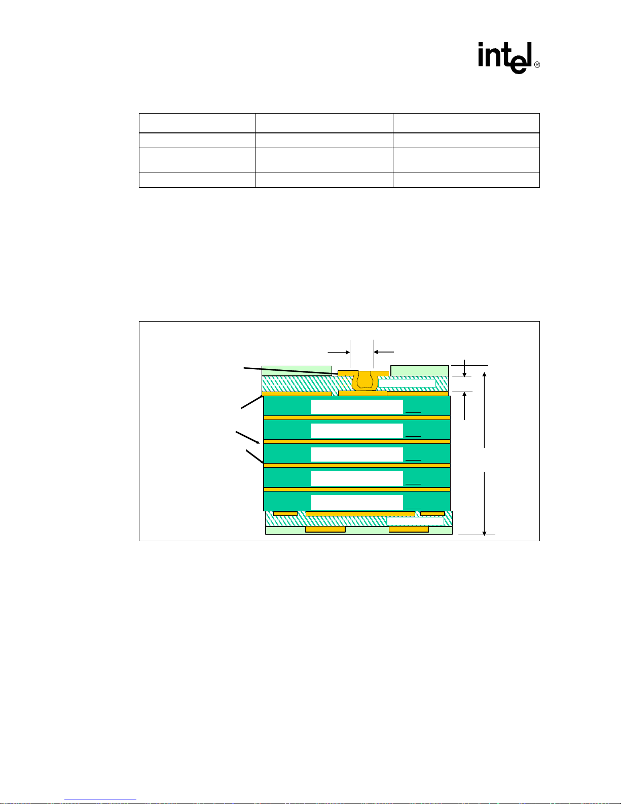
PCB Design Guidelines
Table 2-1. Recommended PCB Design Guidelines (Sheet 2 of 2)
Feature VF-BGA PBGA
Top of Solder Stencil Aperture 0.2790 mm /0.0110 inche s 0.330 mm/0.013 inches
Bottom of Solder Stencil
Aperture
Solder Stencil Thickness 0.1270 mm/0.0050 inches 0.127 mm/.005 inches
0.3000 mm/0.0120 inches 0.356 mm/0.014 inches
2.2.1 PCB Layer Assignment (Stackup)
See Figure 2-1 for illustration of the recommended PCB stackup dimensions and materials. The
illustration shows the recommended PCB layer assignment for an eight-layer PCB using two
power and two ground planes. This configuration provides a continuous VCC_CORE power plane
and a divided I/O power plane for the memory and peripheral domains. See Figure 2-2 for
recommended PCB layer assignment for an eight-layer PCB. See Figure 2-3 for illustration of the
recommended layout of the divided I/O power plane.
Figure 2-1. 1+6+1 uvia PCB Stackup
External Sig. Layers
1 and 8 50% Copper
¼ oz (9um) + plating
Internal Layers
2 thru 7 Copper
Pours 70%
Copper
½ oz (18um)
.102mm (4 mil)
µvia copper
plated
0.13 mm (5.12 mils)
0.13 mm (5.12 mils)
0.13 mm (5.12 mils)
0.13 mm (5.12 mils)
0.13 mm (5.12 mils)
0.070mm 2.8 mils
Resin Coated Copper
FR4
FR4
FR4
FR4
FR4
Resin Coated Copper
0.070mm
2.8 mils
.8-1.0mm
(35 +/-3) mils
For the uvia in pad, design the uvia using RCC (resin-coated copper) surface mount capture pads.
Follow the recommendations for meshing:
• For internal layers: 70% cu = 50 mil (1.27mm) pitch with 14.6 mil (.37mm) trace width.
• For external layers: 50% cu = 50 mil (1.27mm) pitch with 22.6 mil (.57mm) trace width.
Follow the recommendations for surface finish and requirements for physical testing:
• Surface Finish OSP
— Use Organic Solder Preservatives (OSP) Entek 106A.
— Ensure that land pads are as flat as possible (no HASL).
I:2-2 Intel® PXA27x Processor Family Design Guide
Page 25
PCB Design Guid el in es
— Be aware that industry-wide problems with black pad on ENIG (electroless Ni, Immersion
Au) render results useless.
• Physical testing of PCBs
— Moving point probe damages pads that affect mechanical testing results. Therefore, do not
perform physical tests of PC Bs .
Figure 2-2. Recommended PCB Layer Assignment for an Eight-Layer PCB
SIGNAL-1
SIGNAL-2
GROUND-1
VCC-IO (DIVIDED)
VCC_CORE
SIGNAL-3
GROUND-2
SIGNAL-4
Intel® PXA27x Processor Family Design Guide I:2-3
Page 26
PCB Design Guidelines
Figure 2-3. Recommended I/O Power Plane Layout
VCC_MEM
VCC_IO
2.2.2 PCB Component Placement
PCB component placement requires careful planning to consider how signal and power traces map
to the ten power supply domains on the PXA27x processor. See Figure 2-4, Figure 2-5, and
Figure 2-6 for illustrations showing how the processor balls are grouped on the package for each
supply domain. Place the external circuits as close as possible to the output pins of the PXA27x
processor.
VCC_IO
VCC_LCD
VCC_BATT
Recommendations for component placement for the PXA270 processor (VF-BGA, 13 mm x 13
mm) are:
• Place memory components on the left side.
• Place peripherals on the top or bottom side.
• Place the LCD panel in the middle of the right side.
• Place the USIM card interface on the upper right side.
• Place the crystals and power controller signals on the lower right side.
See Figure 2-4, Figure 2-5, and Figure 2-6 for illustrations showing how the VCC_CORE and
VSS_CORE balls are present on all sides of the package. If the VSS references for all domains are
connected to a single common ground plane, connections between all the VSS balls can be made
without difficulty. However, use two power planes to facilitate connection of all VCC supply balls
for each domain. When using two power planes, one continuous plane is assigned to the
VCC_CORE power domain. The second plane is divided for memory and peripheral I/O power
planes (see Figure 2-3).
Place the clock crystals and external load capacitors near the lower right corner of the package as
close as possible to their package balls. If possible, install these components (clock crystals and
external load capacitors) on the bottom of the board under the package to minimize trace
capacitance and noise coupling.
In general, reserve the space on the bottom layer of the PCB under the package for the highfrequency decoupling caps and clock crystals. Install the high-frequency caps and clock crystals on
the bottom layer before installing bulk decoupling caps or other components.
I:2-4 Intel® PXA27x Processor Family Design Guide
Page 27
PCB Design Guid el in es
L
M
Figure 2-4. VF- BG A 13m m x 13 mm Co mp on en t La yo ut Pl ac em en t Gu id e (Top View)
EMORY I/O
MEMORY I/O
1 2 3 4 5 6 7 8 9 101112131415161718192021222324
A
B
C
D
E
F
G
H
J
K
L
M
N
P
R
T
U
V
W
Y
A
A
A
B
A
C
A
D
MEMORY I/O
IO
PERIPHERAL I/OBASEBAND I/F
USB
A
B
C
D
E
F
G
H
J
K
L
M
N
P
R
T
U
V
W
Y
A
A
CONTRO
A
B
A
C
A
D
IO
USIM
LCD
CLOCK &
POWER
CORE
BATT
USB
LCD USIM
BB
MEMSRAM IOPLL
VCC BALL
VSS BALL
Intel® PXA27x Processor Family Design Guide I:2-5
Page 28
PCB Design Guidelines
Figure 2-5. FS-CSP 14mm x 14mm Component Layout Placement Guide (Top View)
IO
USB
1 2 3 4 5 6 7 8 9 10 11 12 13 14 15 16 17 18 19 20
A
B
C
D
E
F
G
H
J
K
L
M
N
P
R
T
U
V
W
Y
1 2 3 4 5 6 7 8 9 10 11 12 13 14 15 16 17 18 19 20
IO
LCDUSIM
v
v
CLOCK & POWER CONTROL
A
B
C
D
E
F
G
IO
H
J
K
L
BB
M
N
P
R
T
U
V
W
Y
MEMORY
CORE
BATT
USB
LCD USIM
BB
MEMSRAM IOPLL
VCC BALL
VSS BALL
RFU
I:2-6 Intel® PXA27x Processor Family Design Guide
Page 29
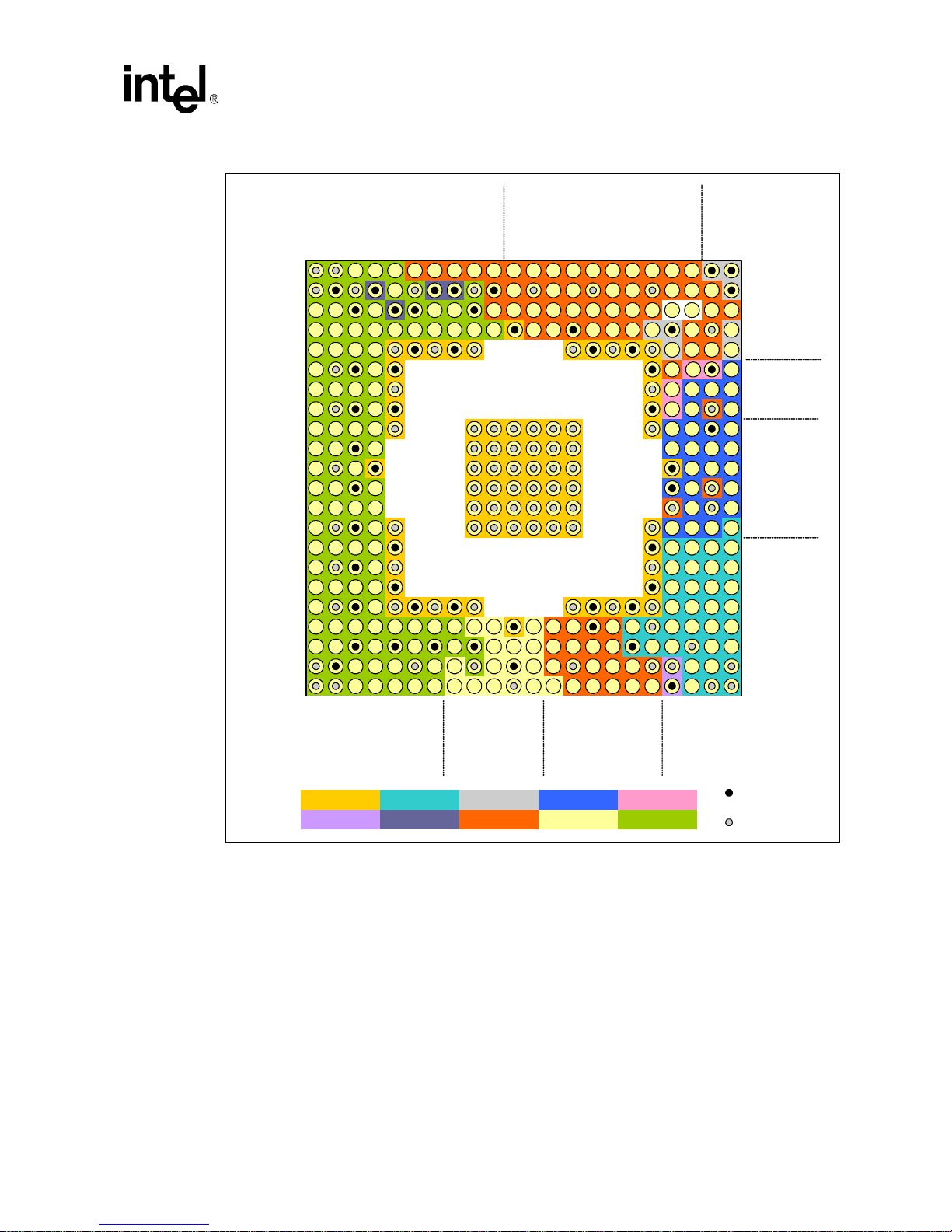
PCB Design Guid el in es
L
M
Figure 2-6. PBG A 23m m x 23m m Co m po ne nt La yo ut Plac em e nt Gu id e (Top View)
EMORY
I/O
MEMORY I/O
1 2 3 4 5 6 7 8 9 10111213141516171819202122
A
B
C
D
E
F
G
H
J
K
L
M
N
P
R
T
U
V
W
Y
A
A
A
B
1 2 3 4 5 6 7 8 9 10111213141516171819202122
IO
USB
A
B
C
D
E
F
G
H
J
K
L
M
N
P
R
T
U
V
CLOCK &
W
Y
CONTRO
A
A
A
B
USIM
LCD
POWER
MEMORY I/O
CORE
2.2.3 PCB Escape Routing
BATT
USB
PERIPHERAL I/OBASEBAND I/F
LCD USIM
BB
VCC BALL
MEMSRAM IOPLL
VSS BALL
One important consideration when implementing chip scale packages (CSP) on a PCB, is the
design of escape routing. Escape routing is the layout of the package signals from underneath the
package to other components on the PCB. Escape routing requires high density interconnect (HDI)
PCB fabrication technology or micro-vias to route signals from the inner rows of balls on these
packages:
• 0.5 mm (0.0197 inches) ball pitch packages (for example, VF-BGA)
• 0.65 mm (0.0256 inches) ball pitch packages (for example, FS-CSP)
Intel® PXA27x Processor Family Design Guide I:2-7
Page 30
PCB Design Guidelines
e
e
2.2.3.1 VF-BGA Escape Routing
This section documents the method of VF-BGA routing along with the recommended dimensions.
Table 2-2. PCB Dimensions for Copper-Defined Land Pads
Feature
A: Land Pad Size
B: Solder Mask Opening
C: Typical Trace Width
D: Reduced Trace Width Between
Land Pads
E: Typical Micro Via (Via-in-Pad)
Drill Size
Finished
.254
(.010)
.381
(.015)
.1016
(.004)
.0635
(.0025)
.102
(.004)
.5 mm
BGA
2
.5 mm
BGA
Designed
.279
(.011)
.381
(.015)
.127
(.005)
.0889
(.0035)
.102
(.004)
NOTES:
1. All dimensions are in mm (inch es).
2. Finished sizes accounts for copper etch.
On the two inner rows of the VF-BGA, route down the signals from the top layer to the inner PCB
layers for routing away from the package. See Figure 2-7 for illustration of the PCB escape routing
using the VF-BGA method.
Figure 2-7. PCB Escape Routing for Copper-Defined Land Pads
Recommended Style:
Copper Defined Land Pads
A: Land Pad Size
A: Land Pad Size
B: Solder Mask Opening
B: Solder Mask Opening
C: Typical Trace Width
C: Typical Trace Width
D: Reduce Trace Width
D: Reduce Trace Width
Between Land Pads
Between Land Pads
Trace on Layer 2
Trace on Layer 2
E: Typical Micro Via (Via-in-Pad) Siz
Top View
Top View
Side View
Side View
I:2-8 Intel® PXA27x Processor Family Design Guide
E: Typical Micro Via (Via-in-Pad) Siz
Land Pad
Land Pad
Land Pad
Solder Mask
Solder Mask
Solder Mask
Page 31

2.2.3.2 FS-CSP Escape Routing
)
This section documents the method of FS-CSP routing along with the recommended dimensions.
Table 2-3. PCB Dimensions for Copper Defined Land Pads
Feature .65 mm BGA
A: Land Pad Size .30 (.012)
B: Solder Mask Opening .432 (.017)
C: Typical Trace Width .100 (.004)
D: Typical Spaces .127 (.005)
E: Trace Width (2 Traces ) .070 (.00275)
F: Spaces (2 Traces) .070 (.00275)
G: Max PTH Via Pad .457 (.018)
H: Max PTH Via Drill Size .25 (.008)
I: Typical Micro Via (Via-in-Pad) Drill Size .127 (.005)
NOTE: All dimens ions are in mm (inches).
On the four inner rows of the FS-CSP, route down the signals from the top layer to the inner PCB
layers fo r rou tin g away from t he pac kag e. Se e Figure 2-7 for illustration of the PCB escape routing
using the FS-CSP method.
PCB Design Guid el in es
Figure 2-8. PCB Escape Routing for Copper Defined Land Pads
A: Land Pad Size
B: Solder Mask Opening
C: Typical Trace Width
D: Typical Spaces
E: Trace Width (2 traces
F: Spaces (2 traces)
G: Max Via Capture Pad
H: Max Via Drill Size
I: Typical Micro Via
(Via-in-Pad) Drill Size
Land Pad
Top View
Side View
Land Pad
Solder Mask
Solder Mask
Intel® PXA27x Processor Family Design Guide I:2-9
Page 32
PCB Design Guidelines
2.2.3.3 PBGA Escape Routing
This section documents the method of PBGA routing along with the recommended dimensions.
Table 2-4. PCB Dimensions for Copper-Defined Land Pads
Feature
A: Land Pa d Size 0.406 (0.016)
B: Solder Mask Opening 0.610 (0.024)
C: Typical Trace Width 0.127 (0.005)
D: Reduced Trace Width Between Land Pads 0.0889 (0.0035)
E: Trace Width (2 Traces) 0.090 (0.0035)
F: Spaces (2 Traces) 0.090 (0.0035)
G: Typical Micro Via (Via-in-Pad) Drill Size N/A
Notes:
1. All dimensions are in mm (inches).
1.0 mm
PBGA
I:2-10 Intel® PXA27x Processor Family Design Guide
Page 33

2.2.4 PCB Ke ep-out Zones
Another key PCB design element is the keep-out zone. The keep-out zone is the distance on each
side of the CSP component to the nearest adjacent component on the board. This keep-out zone
varies depending on the application and is generally much tighter in handheld applications that
require many components in a very small PCB area. While system designers often design keep-out
zones anywhere from 0.100 to 0.050 inches (2.54 mm to 1.27 mm) for embedded applications,
many handheld applications are trending toward 0.025 inches (.635 mm) and smaller. The key
factor to consider is how the component needs to be reworked if the component is replaced. Some
Original Equipment Manufacturers (OEMs) require rework using a hot air nozzle that isolates the
rework area to the specific component that is being reworked. Pay special considerations for
allowing adequate area for the hot air nozzle to surround the CSP being reworked. Currently, there
is no rework procedure for the FS-CSP product.
Another factor that impacts the PCB keepout area requirements is the use of a socket. While
sockets are only used during product development, the sockets require larger keep-out areas to
accommodate mechanical mounting holes. The sockets often require backing plates that prevent
the use of decoupling components under the IC package where the components are most effective.
2.2.5 Recommended Mobile Handset Dimensions
For VF-BGA and FS-CSP packages with bodies >12xY mm and <=14x14 mm, the distance from
board edge to center of package is 14.5 mm (package edge is always 2.5mm from support point).
See Figure 2-9 for illustration of the PCB recommended dimensions.
PCB Design Guid el in es
Figure 2-9. Recommended Mobile Handset Dimensions Diagram
Intel® PXA27x Processor Family Design Guide I:2-11
Page 34

PCB Design Guidelines
2.3 Power Supply Decoupling Requirements
Each major power plane section or feeder trace requires a 4.7 µF or larger bulk decoupling
capacitor near the processor. The processor also requires a 0.1 µF high-frequency decoupling
capacitor on the bottom PCB layer under the package for each group of three to four power supply
pins.
2.4 Thermal Considerations
This subsection describes requirements to ensure the PCB provides adequate thermal dissipation to
ensure compliance with the device operating temperature limitations and long-term reliability.
In battery-powered handset and PDA applications, large heat sinks and forced air cooling are
obviously not practical. For the PXA270 processor, the package heat dissipation is accomplished
primarily using conduction from the 36 center ground balls to the PCB ground plane. For this
reason, the 36 center balls of the VF-BGA package are connected to a solid ground plane under the
package using at least one for every four balls to ensure adequate thermal dissipation.
When the PXA27x processor IC package has a mechanical connection to the product case, this path
also helps dissipate package thermal energy. Refer to Chapter 4 in the Intel
at http://www.intel.com/design/PACKTECH/packbook.htm for more information on package
thermal requirem en ts.
®
Packaging Data Book
2.5 Package to Board Assembly Process
Refer to Chapter 14 in the Intel® Packaging Data Book at http://www.intel.com/design/
PACKTECH/packbook.htm for more information on package to board assembly considerations.
2.6 Silicon Daisy Chain (SDC) Evaluation Units
Intel also offers evaluation units that have been internally shorted together (to the silicon) in a daisy
chain pattern. This ensures that the I/O path of the package is complete through the ball, substrate,
lead beam or bond wire, silicon, and back down through a separate I/O path. These units are useful
for set-up/evaluation of manufacturing equipment.
2.7 Handling: Shipping Media
Intel® VF-BGA and FS-CSPs are shipped in either tape and reel or in mid-temperature thin matrix
trays that comply with JEDEC standards. All JEDEC standard trays have the same 'x' and 'y'
dimensions and are easily stacked for storage and manufacturing.
I:2-12 Intel® PXA27x Processor Family Design Guide
Page 35

PCB Design Guid el in es
2.8 Preconditioning and Moisture Sensitivity
With most surface mount components, if the units are allowed to absorb moisture beyond a certain
point, package damage occurs during the reflow process. Refer to Chapter 8 in the Intel
Packaging Data Book at http://www.intel.com/design/PACKTECH/packbook.htm for package
preconditioning and moisture sensitivity requirements. Specific moisture classification levels are
defined on the box label for the product.
2.9 Tray Specifications
This subsection describes the JEDEC tray specifications for configuring pick and place units. The
JEDEC tray specifications for the VF-BGA are provided in a later revision.
Figure 2-10. FS-CSP (14x14) Tray Specification
®
Intel® PXA27x Processor Family Design Guide I:2-13
Page 36
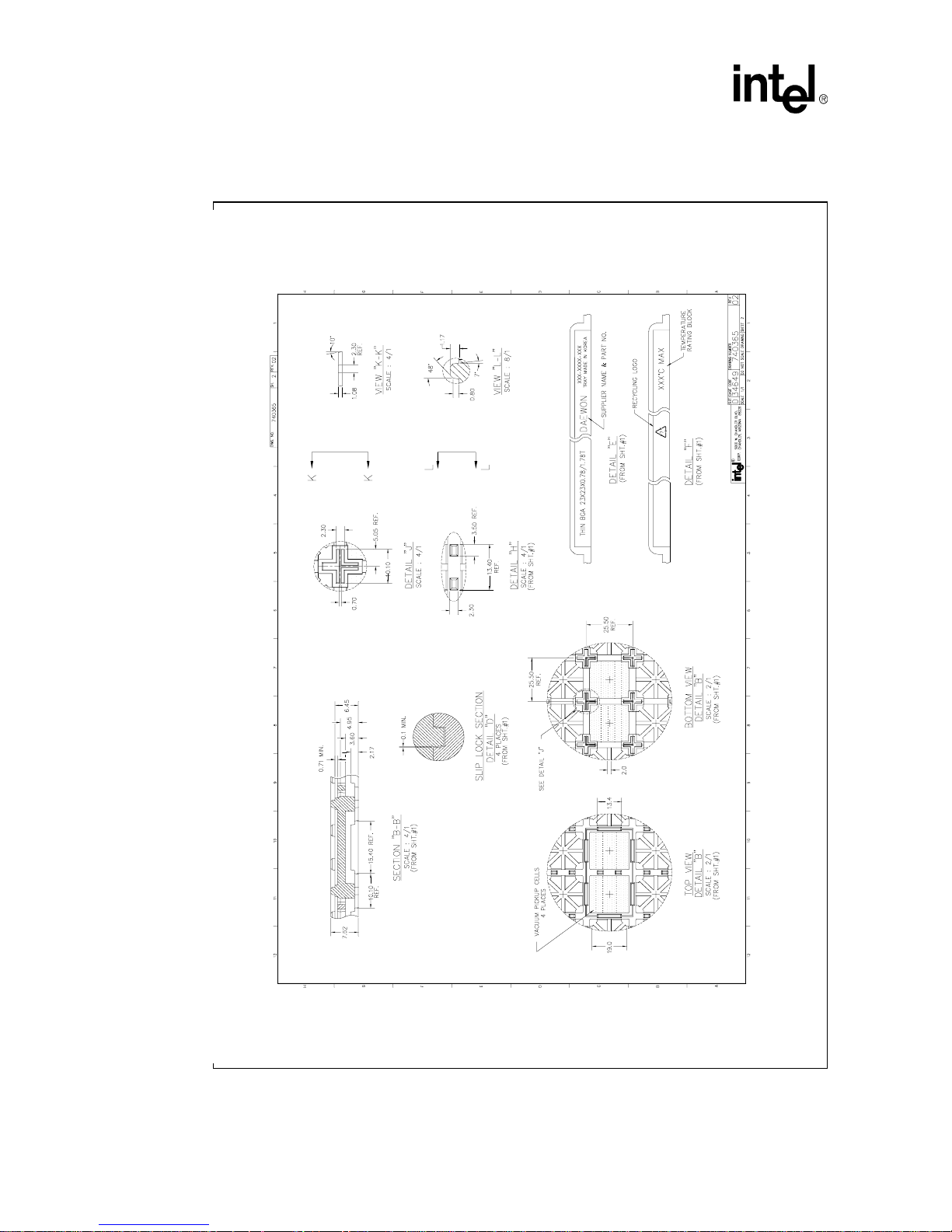
PCB Design Guidelines
Figure 2-11. PBGA (23x23) Tray Specification
I:2-14 Intel® PXA27x Processor Family Design Guide
§§
Page 37

Design Check List 3
For design check list information, refer to the Intel® PXA27x Processor Family Design Check List
Application No te. Se e Table 1-1 for ordering information.
§§
Intel® PXA27x Processor Family Design Guide I:3-1
Page 38

Design Check List
I:3-2 Intel® PXA27x Processor Family Design Guide
Page 39

Mixed Voltage Design Considerations 4
4.1 Overview
The Intel® PXA27x Processor Family (PXA27x processor) uses a complex power management
system that provides the best possible power utilization. The power management system requires
design of several voltage supplies into your system. Use a sophisticated power management
integrated circuit (PMIC) in your system in order to utilize all the power savings possible with the
PXA27x processor.
However, it is not required to incorporate a PMIC into a PXA27x processor-based system. By
using four separate power regulators (optionally five), developing a power management system is
possible for the PXA27x processor. However, the trade-off for such simplicity is increased power
consumption and loss of flexibility in peripheral voltage selection and added requirements for
battery backup.
4.2 Required Power Supplies
See Table 4-1 for the lists of the required power supplies and their associated values for the
PXA27x processor. By careful selection, the three voltage supplies can supply the nine voltages.
Using a 1.1 V, a 1.3 V, and a 3.3 V supply (all regulated at ±10%), satisfy all requirements for the
nine voltage domains.
A fourth voltage regulator supplies the voltage for VCC_BATT. While the supplied voltage is the
same voltage as a regulator already included in the design, a separate regulator must provide the
supplied voltage in order to keep the voltage draw to a minimum. The current required to supply
VCC_BATT is very small and so use a regulator with very small current source capability and
correspondingly small current draw for the voltage supply. The other 3.3 V regulator powers the
peripherals and must have much larger current sourcing capabilities. In a handheld system, the
power draw for the voltage supply is not acceptable.
The trade-off for simplifying these nine supplies to three is that the peripheral supply voltages must
all be 3.3 V. If 3.3 V is unacceptable to the system design, adding a fifth regulator of 1.8 V allows
greater flexibility in the design without dramatically increasing the system cost or complexity. The
addition of a fifth regulator also allows for a mixture of 3.3 V and 1.8 V peripherals for use in the
system design.
Intel® PXA27x Processor Family Design Guide I:4-1
Page 40

Mixed Voltage Design Co ns id er ati on s
Table 4-1. External Power Supply Descriptions
Name Enable Units
VCC_BATT None Sleep-active units, oscillators 3.0 3.0
VCC_IO SYS_EN Peripheral I/O 3.3 3.0, 3.3
VCC_LCD SYS_EN LCD I/O 3.3 1.8, 2.5, 3.0, 3.3
VCC_USB SYS_EN USB I/O 3.3 3.0, 3.3
VCC_MEM SYS_EN Memory Controller Interface 3.3 1.8, 2.5, 3.0, 3.3
VCC_BB SYS_EN Baseband Interface 3.3 1.8, 2.5, 3.0, 3.3
1
VCC_USIM
VCC_PLL P WR _EN Phase Locked Loops 1 .3 1.3
VCC_SRAM PWR_EN Internal SRAM units 1.1 1.1
VCC_CORE PWR_EN All o ther internal units any
NOTES:
1. VCC_USIM must be held to the VCC_IO specification when using alternate function other than USIM signals.
2. Any legal voltage between 0.85 V and 1.55 V is valid. There is no default.
SYS_EN USIM Interface 3.3 1.8, 3.0, 3.3 ±10
Default
Voltage
(V)
Allowed Levels
(V)
2
variable 0.85-1.55 ±10
Tolerance
(%)
±25
±10
±10
±10
±10
±10
±10
±10
4.3 Example Power Supply Utilizing Minimal Regulators
See Figure 4-1 for an example of a power supply system for the PXA27x processor that uses the
minimum number of voltage supplies.
The 1.8 V regulators are shown in dashed lines to indicate where the regulators are used. Use either
the dashed black lines or the dashed lines if that peripheral is used in the system. However, ensure
both voltages (if used) are not connected together.
I:4-2 Intel® PXA27x Processor Family Design Guide
Page 41

Mixed Voltage Design Considerations
M
M
Figure 4-1. Minimal Voltage Regulator Power System Design Example
PWR_EN
ON
1.1V
Regulator
ON
1.3V
Regulator
SYS_EN
ain battery
3.7V
ON
1.8V
Regulator
(optional)
ON
3.3V
Regulator
nReset
VCC_SRAM
VCC_CORE
(drowsy)
VCC_PLL
VCC_IO
VCC_ME
VCC_BB
VCC_USIM
VCC_LCD
Intel® PXA27x Processor Family Design Guide I:4-3
3.3V
Regulator
Supe
rCap
Low
Reference
voltage*
High Reference voltage**
* Battery level where system must enter deep sleep until main battery is
recharged.
** Battery level where system should save state and enter sleep.
VCC_BATT
BATT_FAULT
VCC_FAULT
Page 42

Mixed Voltage Design Co ns id er ati on s
4.4 Cautions
Observe the following cautions for proper operation and reliability of the PXA27x processor:
• All power domains are equal to or lower than VCC_IO (excluding VCC_USB).
• The application of VCC_BATT to the PXA27x processor from a state where there was no
voltage applied to VCC_BATT is referred to as start-of-date. If only VCC_BATT is applied at
the start-of-date, the current internal state of the PXA27x processor causes the current draw to
be higher than when the PXA27x processor is in deep sleep mode. Such a situation is
undesirable for systems that are production units, therefore, do not use these units
immediat ely. Afte r the ba ckup ba tter y is ini tial ly inst alle d, if th e devi ces are not bro ught in to at
least deep sleep mode through software, the backup battery experiences drainage. To avoid
drainage of backup battery and to allow the backup battery to remain connected after
production, boot the device and then place the device in deep sleep mode.
§§
I:4-4 Intel® PXA27x Processor Family Design Guide
Page 43

Power Measurements 5
5.1 Overview
The Intel® PXA27x Processor Family (PXA27x processor) employs a complex power
management system that provides the best possible power utilization. Take additional steps to
minimize total power consumption. This chapter describes recommended methods for measuring
power and provides the recommended steps in detail to minimize overall power usage.
5.2 Measurement Guidelines
There are two methods for measuring power on each of the power domains of the PXA27x
processor:
• Measuring voltage across a series resistor
• Measure current directly with a current meter in series
The development design must allow for each power domain of the PXA27x processor to receive
power inde pen dent ly t hro ugh a dedi cat ed sh unt jump er fo llo wed by a shu nt r esi sto r for eac h powe r
domain to use the two recommended methods.
No matter what method is used, measure the voltage at the PXA27x processor and monitor the
voltage across all power domains during each measurement.
5.2.1 Measure Voltag e Across a Series Resistor
This method measures voltage across a series resistor and calculates the total power consumed.
This method involves using equipment to measure a voltage across a known series resistance and
calculating the current works for calculating power during normal mode operations. This method is
preferred for high current power supplies such as VCC_CORE. However, this method is not ideal
for measuring low power due to the limitations of the equipment being used to measure power. The
voltage drop when measuring low power could be too small for detection by the digital volt meter
(DVM).
5.2.2 Measure Current Directly with a Current Meter in Series
This method measures current directly with a current meter in series, then calculates total power
consumed. This methods works for all power modes, but could be too invasive and negatively
affect the functioning of the PXA27x processor in some cases.
Use the following procedure to measure current directly with a current meter is series:
1. Check the internal resistance for the current meter.
2. Calculate the effective voltage drop across the internal resistance based of the maximum
expected curren t.
3. Verify that the voltage drop minus the voltage supplying the voltage domain being tested does
not fall below the required V
for that domain.
in
Intel® PXA27x Processor Family Design Guide I:5-1
Page 44

Power Measurements
Some DVMs have an internal resistance of 1.0 to 2.0 Ω that could cause the V
minimum required supply voltage depending on the power mode being used. If V
minimum required supply voltage, the external power supply would be required to compensate.
The method of measuring current directly with a current meter in series is preferred for low current.
Use the lowest possible range supported by the DVM. Avoid changing ranges during the operation
of PXA27x processor.
to drop below the
in
drops belo w the
in
5.3 Achieve Minimum Power Usage During All Power
Modes
Methods for achieving the lowest power usage during all power modes:
• Connecting the crystal signals to an external differential oscillator achieves the least amount of
power consumed by the PXA27x processor. Yet, the power consumed by the differential
oscillator are considered for total system power usage. Exercise special care when selecting an
external oscillator rather than an external crystal. Verify that the external oscillator is equally
or more efficient than the PXA27x processor using a crystal.
• Design the system so that all power domains uses the lower voltage level supported within the
specifications, that is, VCC_MEM – 1.8 V.
• Ensure I/O voltage levels track power domain levels, that is, for VCC_MEM – 1.8 V, all MD
pins must drive at 1.8 V, otherwise it could cause negative current.
• Ideally, the system design allows measurements of power across all domains individually,
helping the designer in isolating high current problems down to a specific voltage domain.
• Disable all internal pull-ups/pull-downs on GPIO, which is accomplished through PTCR
register settings.
• Clearly define clock and memory controller settings.
5.4 Achieve Minimum Power Usage During Deep Sleep
Methods for achieving lowest power usage during deep sleep power modes:
• Ground all non VCC_BATT power domains to enable the designer find the lowest power
consumption and validate the design.
• Monitor and register temperature sensitivity.
• Ensure TDI and TMS pins are pulled high or left floating.
• Ensure the USBC differential inputs (USBCP and USBCN) are pulled high or left floating
with no impact to OTG pins.
• Enable DC-DC int ern al pow er supp ly.
• Ensure DC convert er cap s are con ne cte d prop erl y.
I:5-2 Intel® PXA27x Processor Family Design Guide
Page 45

Power Measurements
5.5 Achieve Minimum Power Usage During Sleep
Methods used for achieving lowest power usage during sleep power modes:
• Ground SRAM/PLL/Core power domains to enable the designer find the lowest power
consumptio n and val ida te the desig n.
• Configure GPIO signals of the PXA27x processor as input and drive a low from external
source. Programmers can use PGSR/FS (GPIOs in O/P mode).
• Ensure TDI and TMS pins are pulled high or left floating.
• Ensure the USBC differential inputs (USBCP and USBCN) are pulled high or left floating
with no impact to OTG pins.
• Enable DC-DC internal power supply.
5.6 Achieve Minimum Power Usage During Standby
Methods used to achieve lowest power usage during standby power modes:
• Ensure VCC_CORE and VCC_SRAM voltage is at 1.1 V.
• Configure GPIO signals of the PXA27x processor as input and drive a low from external
source. Programmers can use PGSR/FS (GPIOs in O/P mode).
• Ensure TDI and TMS pins are pulled high or left floating.
• Ensure the USBC differential inputs (USBCP and USBCN) are driven high or left floating
with no impact to OTG pins.
5.7 Achieve Minimum Power Usage During Idle/13M/
Run/Turbo
Methods used to achieve lowest power usage during idle, 13M, run and turbo power modes:
• Run/Turbo
— Set auto power down (APD) bit.
— Enable both instruction and data caches.
— Use read allocate/write back (caching policy).
• 13M
—Disable PLLs.
• Idle
— Ensure interrupts are disabled to prevent unexpected walk-ups.
Intel® PXA27x Processor Family Design Guide I:5-3
§§
Page 46

Power Measurements
I:5-4 Intel® PXA27x Processor Family Design Guide
Page 47

Introduction to Part II 1
The chapters in Part II of the Design Guide describe the design recommendations and constraints
related to specific on-chip peripherals of Intel
These recommendations include information regarding signal connections, block diagrams, and
notes related to system implementation.
The examples and schematics in this document represent one of the many methods to connect and
use the peripherals described. This does not imply that the method recommended in this document
is the best or sole method of connecting and using the peripherals. Carefully consider the
recommendations to ensure they are appropriate for your particular design.
Each peripheral is described in a separate chapter. The chapters in Part II are organized similarly to
the chapters in the Intel
to make the information easier to locate. If multiple configurations of a peripheral exist, all
possible configuration combinations are shown. However, not all configuration combinations are
described.
The recommendations provided here are intended to guide and assist in the implementation of the
peripherals, but they are not necessarily a “drop-in” solution for all designs. The use of this manual
and the information contained within must not replace careful consideration of system
requirements and good design practices.
®
PXA27x Processor Family Developers Manual and use a similar format
®
PXA27x Processor Family (PXA27x processor).
§§
Intel® PXA27x Processor Family Design Guide II:1-1
Page 48

Introduction to Part II
II:1-2 Intel® PXA27x Processor Family Design Guide
Page 49

Package and Pins 2
Refer to Intel® PXA270 Processor Electrical, Mechanical, and Thermal Specification and Intel
PXA27x Processor Family Electrical, Mechanical, and Thermal Specification for complete
information on processor signals, signal-to-package ball mapping, and package mechanical
specifications for Intel
®
PXA27x Family Processor (PXA27x processor).
§§
®
Intel® PXA27x Family Processor Design Guide II:2-1
Page 50

Package and Pins
II:2-2 Intel® PXA27x Family Pr oc es so r De sig n Gu id e
Page 51

Clocks and Power Interface 3
3.1 Overview
This chapter describes design recommendations and requirements for the external clock and power
supply components connected to Intel
3.2 Signals
The following sections describes signals required for the clock and power interface.
3.2.1 Clock Interface Signals
See Table 3-1 for definition of the PXA27x processor clocks signals.
Table 3-1. Clock Interface Signals (Sheet 1 of 2)
Name Type Definition
nRESET Input
nRESET_OUT Output
GPIO<n> Bidirectional
GPIO<3> Bidirectional The GPIO<3> pin is used as standby, sleep, and deep-sleep wake-up sources.
GPIO<1:0> Bidirectional
PXTAL_IN Input
PXTAL_OUT Analog
CLK_PIO Bidirectional
TXTAL_IN Input
TXTAL_OUT Analog
Active-low input
Indicates to the processor to enter hardware-reset state.
Active-low output
Indicates to the system that the processor is in a reset state (configurable for
sleep and deep-sleep exit and GPI O rese t).
The GPIO<n> pins are used as standby and sleep wake-up sources.
For possible values for n, refer to the GPIO chapter in the Intel
Processor Family Deve lopers Manual.
The GPIO<1:0> pins are used as:
• Standby and sleep/deep-sleep wake-up sources
• Deep-sleep wake -u p sour ces, after nBATT_FAULT or nVDD_FAULT is
asserted
Connect to an external 13-MHz crystal or to an external clock source.
For more informatio n, ref er to Section 3.5.1, “Clock Interface.”
Connect to an external 13-MHz crystal or to an external clock source that is
complementary to PXTAL_IN or floated.
Drives a buffered version of the PXTAL_IN oscillator input or used as a clockinput alternative to PXTAL_IN.
Connect to an external 32.768-KHz crystal or to an external clock source that is
distributed to the timekeeping control system and power-management unit. Refer
to Section 3.5.1, “Clock Interface,” for more information.
Connect to an external 32.768-KHz crystal or to an external clock source that is
complementary to TXTAL_IN or floated.
®
PXA27x Processor Family (PXA27x processor).
®
PXA27x
Intel® PXA27x Processor Family Design Guide II:3-1
Page 52

Clocks and Power Interface
Table 3-1. Clock Interface Signals (Sheet 2 of 2)
CLK_TOUT Output Drives a buffered and inverted version of the TXTAL_IN oscillator input.
Input during power-on or hardware reset that indicates whether the processor
CLK_REQ Bidirectional
CLK_EXT Input
oscillator clock input comes from PXTAL_IN (CLK_REQ low) or CLK_PIO
(CLK_REQ floating). If CLK_PIO is the processor oscillator input, CLK_REQ
becomes an output indicating when the processor oscillator is required. For more
information, refer to Section 3.5.1, “Clock Interface.”
Used by the Mobile Scalable Link (MSL), SSP or operating system (OS) timer
module as a clock input (optional).
3.2.2 Power Manager Interface Control Signals
The PXA27x processor has an internal power manager unit (PMU) and a set of I/O signals for
communicating with an external power management integrated circuit (PMIC). The I/O signals are
active for initial power-up, certain reset events, device on/off events, and transitions between some
operating modes. There are also two Fault signals (nBATT_FAULT and nVDD_FAULT) required
from the PMIC to communicate the onset of power supply problems to the processor.
The PXA27x processor communicates to the power controller using the signals defined in
Table 3-2.
Table 3-2. Power Controller Interface Signals
Signal Definition Active State S ig n al Dir ect io n
PWR_EN Power Enable High Output
SYS_EN System Enable High Output
2
PWR_SCL I
PWR_SDA I
nRESET
nBATT_FAULT
nVDD_FAULT
PWR_CAP<3:0>
PWR_OUT
48_MHz
† Input and Output refers to signal direction to or from the PXA27x pro cessor.
C bus clock Clock Output
2
C bus data — Bidirectional
Forces an unconditional hardware
reset
Indicates main battery removed or
discharged
Indicates one or more supplies are out
of regulation
The PWR_CAP pins connect to
external capacitors that are used with
on-chip DC-DC converter circuits to
achieve very low power in sleep
mode.
Connects to an external isolated
capacitor.
48 MHz output clock
Used to generate peripheral timing
from the 312-MHz periph era l cloc k
†
Low Input
Low Input
Low Input
—Analog
—Analog
Clock Output
II:3-2 Intel® PXA27x Processor Family Design Guide
Page 53

3.2.3 Power Enable (PWR_EN)
PWR_EN is an active-high output from the PXA27x processor (input to the PMIC) that enables the
external core power supplies (VCC_CORE, VCC_SRAM, VCC_PLL.) De-asserting PWR_EN
indicates to the external regulator that the processor is going into sleep mode and that the lowvoltage core power supplies are removed.
When PWR_EN is asserted, normal operation resumes and the PMIC turns on the core (lowvoltage) supplies. The power controller must preserve, during sleep or deep sleep, the previous
state of its regulators including the voltage for the core. Then, on resumption of core power, the
regulators return to their last known voltage levels.
3.2.3.1 System Power Enable (SYS_EN)
SYS_EN is an active-high output from the PXA27x processor (input to the PMIC) that enables the
external system power supplies. De-asserting SYS_EN indicates to the power supply that the
processor is going into deep sleep mode, allowing the removal of high-voltage system power
supplies (VCC_IO, VCC_LCD, VCC_MEM, VCC_USIM, VCC_BB, and VCC_USB). When
powering on and off the various voltage domains, assertion and de-assertion of SYS_EN must
occur in the correct sequence with PWR_EN to ensure the correct sequencing of power supplies.
When SYS_EN is asserted, normal operation resumes and the PMIC turns on the system I/O (highvoltage) supplies. Then, when PWR_EN is asserted, the PMIC turns on the core (low-voltage)
supplies. The power controller must return all system I/O voltages to their pre-deep sleep mode
levels.
Clocks and Power Interface
3.2.3.2 Power Manager I2C Clock (PWR_SCL)
The PWR_SCL signal is the power manager I2C clock output to the external PMIC. The I2C serial
bus must operate at a minimum 40 KHz and optionally be capable of operating at 160 KHz clock
rate.
3.2.3.3 Power Manager I2C Data (PWR_SDA)
The PWR_SDA signal is the power manager I2C data pin to the external PMIC. It functions like an
open-drain signal so that either component pulls it down to a logic-low level.
3.2.3.4 nVDD_FAULT
nVDD_FAULT signals the PXA27x processor that one or more of its currently enabled supplies
are below the minimum regulation limit (supplies that are not enabled, do not cause
nVDD_FAULT assertion.) Functionally, nVDD_FAULT indicates to the processor when it is safe
to exit sleep or when it must enter sleep (using the mechanism selected by the PMCR[xIDEA] bits)
until the SYS_DEL timer expires. The PXA27x processor also has a configuration bit that allows
nVDD_FAULT to be ignored in sleep mode. Refer to Intel
Mechanical, and Thermal Specification and Intel
Mechanical, and Thermal Specification for SYS_DEL and PWR_DEL timing specifications.
®
PXA27x Processor Family Electrical,
®
PXA270 Processor Electrical,
Intel® PXA27x Processor Family Design Guide II:3-3
Page 54

Clocks and Power Interface
3.2.3.5 nBATT_FAULT
nBATT_FAULT indicates that the main battery is low or is being removed from the device,
conveying to the PXA27x processor that power will be depleted shortly. During this time, the
processor operates for a limited time from a Lithium/Lithium manganese “coin-cell” backup
battery, or from a “super cap” that supplies the processor only for a few cycles of full-run power.
In the event of nBATT_FAULT assertion, the PXA27x processor enters an emergency form of
sleep. In emergency sleep, the only handshaking is with external SDRAM memory (putting it into
self-refresh mode.) This communication between the PXA27x processor and the external SDRAM
memory ensures that memory contents are preserved, if possible. Obviously, the refresh currents
eventually depletes the cap or backup battery, but not as fast as the PXA27x processor in run mode.
Supporting these features must be understood at both the board level design and by the power
controller/regulator.
Note: The processor does not recognize a wake-up event while nBATT_FAULT is asserted.
3.3 Block Diagram
See the system schematic in Figure 3-1 for illustration of one recommended configuration for
connecting the PXA27x processor directly to the backup battery. In such a configuration, the
regulated main battery powers VCC_BATT through regulator U7 and the backup battery powers
VCC_BATT when the main battery discharges. Regulator U7 also charges the backup battery. The
output voltage of U7 must ensure VCC_BATT remains:
• Between 2.25 V and 3.75 V when VCC_IO is disabled
• Within 200 mV of VCC_IO when VCC_IO is enabled
D1 protects regulator U7 from the back current when the backup battery drives VCC_BATT to a
higher potential than the output of U7. D3 and R2 limit over-charging current to the backup battery.
While the processor is powering up the VCC_REG domain from VCC_BATT, D2 and R1 prevent
the PXA27x processor from over-charging the backup battery. See Figure 3-1. This preventive
action from D2 and R1 occurs if an input signal on the VCC_REG domain is driven above the
backup battery voltage.
II:3-4 Intel® PXA27x Processor Family Design Guide
Page 55

Figure 3-1. Typical Battery and External Regulator Configuration
Clocks and Power Interface
V1
Main Battery
U2
ENABLE
IN
OUT
1.8V, 2.5V, 3.0V or 3.3V Regulator
U3
ENABLE
IN
OUT
1.8V, 3.5V, 3.0V or 3.3V Regulator
U4
ENABLE
IN
OUT
3.3V or 3.0V Regulator
U6
ENABLE
IN
OUT
1.1V Fixed Regulator
U5
ENABLE
IN
OUT
1.3V Fixed Regulator
U8
ENABLE
IN
OUT
0.85V - 1.30V Adj. Regulator
POWER_SWITCH
ADAPTER_PWR
U7
IN OUT
Fixed Regulator
SYS_EN
SYS_EN
SYS_EN
3.0V
1.8V
PWR_EN
PWR_EN
PWR_EN
ALL_REGULATORS_OK
U9
OUT
IN1
IN2
ENABLE
I2C Controlled S witch
D1
PWR_ADAPTER_DETECTED
SYS_EN
SYS_EN
PWR_EN
PWR_EN nBATT_FAULT
REG_OK
MAIN_BATT
PWR_SW _IN I2C_CLK
LOGIC_VCC
Powe r Con trol In terface
U10
nVDD_FAULTSYS_EN
Fault Monitor
U11
PWR_SW _OUT
nRESET
I2C_DATA
PXA27x
U1
VCC_BB
VCC_LCD
VCC_MEM
VCC_IO
VCC_USIM
UVSO
nUVS1
nUVS2
VCC_SRAM
VCC_PLL
VCC_CORE
SYS_EN
PWR_EN
nBATT_FAULT
nVDD_FAULT
nRESET_OUT
nRESET
PWR_SCL
PWR_SDA
GPIO0
GPIO1
VCC_BATT
D3
R2
D2
R1
Intel® PXA27x Processor Family Design Guide II:3-5
V2
Backup Battery
Page 56

Clocks and Power Interface
3.4 Layout Notes
Two external power capacitors must be connected to the PXA27x processor PWR_CAPx signals.
The capacitors, C2 and C3, must be populated to achieve power efficiency using the DC-DC
converter.
The sleep mode DC-DC converter requires three external components:
• C1: 0.1 µF capacitor connected to the PWR_OUT pin and ground (not optional)
• C2: 0.1 µF capacitor connected between the PWR_CAP0 and PWR_CAP1 pins
• C3: 0.1 µF capacitor connected between the PWR_CAP2 and PWR_CAP3 pins
The sleep/deep-sleep mode DC-DC converter is enabled by setting the DC_EN bit field in the
Power Manager General Configuration register.
The DC-DC converter is used when all of these conditions apply:
Note: The sequence of setting these conditions is unimportant.
• The PXA27x processor is in sleep or deep-sleep mode.
• The PXA27x processor oscillator (13.000 MHz) is disabled.
• None of the internal SRAM banks, CPU, power island, or peripheral units are in a state-
retaining mode.
• The power manager I
The capacitors, C2 and C3, must be low equivalent series resistance (ESR), ceramic, unpolarized
capacitors. No other connections are allowed on the PWR_OUT and PWR_CAP<3:0> pins.
2
C, JTAG, and timer are inactive.
3.5 Modes of Operations
This section provides detailed information on different modes of operations for both the clock and
power interface.
3.5.1 Clock Interface
The PXA27x processor requires a 13-MHz timing reference that generates all core and most
peripheral timing. While the real-time clock is operated from the 13-MHz reference to save cost
and space in systems that do require high timekeeping accuracy, most systems use a 32.768-KHz
timing reference. Using a 32.768-KHz timing reference dramatically reduces power consumption
in the standby, sleep, and deep sleep operating modes and provides better accuracy with the realtime clock.
Both timing references are generated using a crystal with the on-chip oscillator or externally by
clock oscillators. This flexibility eliminates the need for duplicate oscillators in systems that
already use a 13.000-MHz or a 32.768-KHz oscillator. Additionally, when the PXA27x processor
generates either clock using its oscillator, this clock drives the clock inputs of other system
components such as a cellular baseband processor.
II:3-6 Intel® PXA27x Processor Family Design Guide
Page 57

Clocks and Power Interface
3.5.1.1 Using the On-Chip Oscillator with a 32.768-KHz Crystal
The Intel® PXA270 Processor Electrical, Mechanical, and Thermal Specification and Intel®
PXA27x Processor Family Electrical, Mechanical, and Thermal Specification provide
specifications for the 32.768-KHz crystal. To use the on-chip crystal oscillator, connect the 32.768KHz crystal between the TXTAL_IN and TXTAL_OUT pins of the processor. The on-chip
oscillator provides the required load capacitance, so do not connect external load capacitors to the
crystal. Place the crystal as close as possible to the TXTAL_IN and TXTAL_OUT pins of the
processor to minimize PCB trace length and capacitance. Route these traces parallel to each other
on the same PCB layer. If the 32.768-KHz oscillator output are used by other components in the
system, connect these inputs to the processor CLK_TOUT output and enable it. Do not attempt to
connect an external load directly to the TXTAL_OUT pin.
3.5.1.2 Using an External 32.768-KHz Clock
When using an external clock oscillator to supply the RTC timing, power up the oscillator from the
same source that is driving the VCC_BATT supply input. Connect the oscillator output to the
TXTAL_IN pin.
Note: The oscillator-output-high-drive level must be between 80% of VCC_BATT (0.8 x VCC_BATT)
and VCC_BATT. Similarly, the oscillator-output-high-drive level must be between 80% of
VCC_BATT (0.8 x VCC_BATT) and VCC_BATT. TXTAL_OUT is left floating or driving
complimenta ry to TX TAL_IN.
3.5.1.3 Using the On-Chip Oscillat or with a 13.000-MHz Crystal
The Intel® PXA270 Processor Electrical, Mechanical, and Thermal Specification and Intel®
PXA27x Processor Family Electrical, Mechanical, and Thermal Specification provide
specifications for the 13.000-MHz crystal. To use the on-chip crystal oscillator, connect the
13.000-MHz crystal between the PXTAL_IN and PXT AL_OUT pins of the processor. To select the
internal oscillator, ground the CLK_REQ input. The on-chip oscillator provides the required load
capacitance, so do not connect an external load capacitors to the crystal. Place the crystal as close
as possible to the PXTAL_IN and PXTAL_OUT pins of the processor to minimize PCB trace
length and capacitance. Route these traces parallel to each other on the same PCB layer. If the
13.000-MHz oscillator output is used by other components in the system, connect these inputs to
the processor CLK_PIO output and enable it. Do not attempt to connect an external load directly to
the PXTAL_OUT pin.
Intel® PXA27x Processor Family Design Guide II:3-7
Page 58

Clocks and Power Interface
3.5.1.4 Using an External 13.00-MHz Clock
When using an external clock oscillator to supply the 13-MHz timing, power the oscillator from the
same source driving the VCC_BATT supply input. Connect the oscillator output to the CLK_PIO
pin. Leave the CLK_REQ pin floating or connect it to the external oscillator’s output enable input.
During reset, sample the CLK_REQ pin to determine the oscillator configuration. During reset,
when not driven externally, CLK_REQ pulls high internally. When CLK_REQ is pulled high
internally, it allows CLK_PIO to be configured as an input and makes CLK_REQ an active high
output enable to control the external oscillator. Refer to Intel
Mechanical, and Thermal Specification and Intel
Mechanical, and Thermal Specification for CLK_REQ timing specification.
Notes:
• The oscillator output high drive level must be between 80% of VCC_BATT (0.8 x
VCC_BATT) and VCC_BATT. Similarly, the oscillator output low drive level must be
between VSS and 20% of VCC_BATT (0.2 x VCC_BATT).
• CLK_REQ must not be pulled high or driven high externally.
3.5.2 Power Interface
®
®
PXA27x Processor Family Elec tri ca l,
PXA270 Processor Electrica l,
To enable low power system design, the PXA27x processor has nine separate power supply
domains for the processor core, memory, and peripherals. All functional units, within a power
domain, connect to the same power supply and are powered up and down together. This
architecture provides flexibility in system configuration (for example, selection of different I/O
voltages for memory and peripherals) and efficient power management (for example, flexibility in
selecting which peripherals are powered at the same time).
In a complete system, there are other components besides the processor such as DRAM and flash
memory, audio CODECs, touchscreen controllers, and specialized companion chips with their own
unique power requirements. In many designs, a highly-integrated power controller supplies power
for the processor and other components, particularly those that interface directly to the PXA27x
processor. An advanced power controller contains circuitry for charging batteries, for powering the
display panel, and includes other analog functions as required by the system. The PXA27x
processor provid es sev era l dedi cat ed con tro l sign als as well as an Int er-Integ rat ed Circu it (I
interface to communicate with an external power management integrated circuit (PMIC).
3.5.2.1 Power Supplies
A summary of the voltage and tolerance requirements for each external supply input is provided in
the Intel
PXA27x Processor Family Electrical, Mechanical, and Thermal Specification. In systems which
dynamically adjust the processor power supply and clock frequency to minimize power, there are
additional requirements for the VCC_CORE power supply. Refer to the Intel
Family Power Requirements Application Note document for more information.
®
PXA270 Processor Electrical, Mechanical, and Thermal Specification and Intel®
2
C)
®
PXA27x Processor
II:3-8 Intel® PXA27x Processor Family Design Guide
Page 59

Clocks and Power Interface
3.5.2.1.1 Power Supply Design Requirements
VCC_BATT powers the real time clock (RTC) and power management circuitry during initial
power-on, sleep, deep sleep and sleep wake-up, so the RTC must remain powered from the backup
battery when the main power source is discharged or removed. When the system main battery is
installed, VCC_BATT must be driven by a regulator whose output matches the output of VCC_IO
regulator. This ensures that VCC_IO and VCC_BATT remain within 200 mV of each other when
the VCC_IO regulator is enabled. Power the external output drivers for the logic signals nRESET,
nVDD_FAULT, nBATT_FAULT, PWR_SDA, GPIO0 and GPIO1 from the VCC_BATT supply.
This also applies to all other digital outputs such as the JTAG signals driving PXA27x processor
inputs on the VCC_REG domain. Refer to Figure 3-1. Any device that ha s a di git al in put driv en by
a PXA27x processor digital output and is powered from the VCC_REG domain, must tolerate
output high drive levels between 2.25 V and 3.75 V.
VCC_PLL must driven by a regulator which cannot be shared with any other devices.
VCC_IO is the fixed sup pl y for stan da rd CM O S I/O interfacing to external comp one nts . VC C_ IO
must be the highest potential in the system (excluding VCC_BATT and VCC_USB) and must be
turned on at the same time or before the other supplies enabled by SYS_EN. VCC_IO are
connected to any of the VCC_USB, VCC_LCD, VCC_MEM, VCC_BB, or VCC_USIM supplies
as long as none of these supplies are driven at a voltage higher than VCC_IO.
Caution: When VCC_IO is connected to a VCC_USIM supply with voltage higher than 3.0V, it does not
damage the silicon, but exceeds the USIM card specification, which in turn can cause damage to
USIM card.
VCC_IO must be enabled when SYS_EN is asserted and disabled when SYS_EN is de-asserted.
The I/Os for external components connected to the corresponding I/O pins on the PXA27x
processor must be supplied from the same regulator generating VCC_IO. VCC_USB powers the
differential I/O signals for the USB client and host 1 interface. Be aware that the USB differential
signals D+ and D- are out of compliance with the USB specification if VCC_USB is below 2.8 V.
The +5 V V
source from USB host controller, which is available for bus-powered peripherals,
BUS
must be supplied from an external source.
§§
Intel® PXA27x Processor Family Design Guide II:3-9
Page 60

Clocks and Power Interface
II:3-10 Intel® PXA27x Processor Family Design Guide
Page 61

Internal SRAM 4
There is no existing hardware requirements related to the internal SRAM since the internal SRAM
is not accessible using an external signal. This chapter provides information on the affects of the
power capacitors on the internal SRAM.
4.1 Overview
The internal memory block provides 256 Kbytes of memory-mapped SRAM. The internal memory
is divided into four banks, each is a 64 Kbytes bank. The memory has special power-saving
features, including individual power management for each memory bank.
4.2 Signals
I/O signals are not assoc iat ed wit h the intern al me mo ry blo c k .
4.3 Block Diagram
The internal memo ry blo ck has six ma jor modu les :
• System Bus Interface
• Control/Status Registers
• Power Management
• Memory Bank Mu xi ng and Con tro l
• Queues
• Four Memory Banks
See the internal memory block diagram in Figure 4-1.
Intel® PXA27x Processor Family Design Guide II:4-1
Page 62

Internal SRAM
M
Figure 4-1. Internal SRAM Block Diagra m
To Clocks/Power
anagement Blcok
Power Management
Control/Status
Registers
To System Bus
System Bus Interface
Queue
Bank 0
Bank Muxing and Control
QueueQueueQueue
Bank 1 Bank 2 Bank 3
Memory Array
ISRAM_001_P2
4.4 Layout Notes
The power caps allows the internal SRAM to be powered up during sleep. Refer to Section 3.4 for
detailed information.
§§
II:4-2 Intel® PXA27x Processor Family Design Guide
Page 63
DMA Controller Interface 5
This chapter describes the procedures for interfacing the DMA controller of the Intel® PXA27x
Processor Family (PXA27x processor) with companion chips using the fly-by and flow-through
DMA transfer.
5.1 Overview
The PXA27x processor contains a DMA controller that transfers data to and from the memory
system in response to requests generated by peripherals or companion chips. These peripheral
devices and companion chips do not directly supply addresses and commands to the memory
system. Instead, the addresses and commands are maintained in 32 DMA channels within the
DMA controller. Every DMA request from the peripheral device and companion chip generates a
memory bus cycle. The DMA controller of the PXA27x processor supports both flow-through and
fly-by transfers.
5.2 Signals
See Table 5-1 for the list of signals used to interface to the DMA controller.
Table 5-1. DMA Interface Signals
Signal Name Type Description
DREQ<2:0> Input
DVAL<1:0> Output
External Companion Chip Request
The DMA contr olle r detect s the po siti ve edge of the DR EQ
signal to log a request. The external companion chip
asserts the DREQ signal when a DMA transfer request is
required. The signal must remain asserted for four
MEM_CLK cycles to allow the DMA controller to recognize
the low-to-high transition. When the signal is de-asserted,
the signal must remain de-asserted for at least four
MEM_CLK cycles. The DMA controller registers the
transition from low to high to identify a new request.
The external companion chip need not wait until the
completion of the data transfer before asserting the next
request. This companion chip has up to 31 outstanding
requests on each of the DREQ<2:0> pins. The number of
pending requests are logged in special status registers,
DRQSRx.
Requests on pins DREQ<1:0> are used for data transfers
in either fly-by or flow-through modes.
Request s on p i ns D R EQ <2> ar e u sed f o r d a ta t ra ns fe rs i n
flow-through mode only.
External Companion Chip Valid
The memory controller asserts DVAL to notify the
companion chip. Either data must be driven or is valid.
Intel® PXA27x Processor Family Design Guide II:5-1
Page 64

DMA Controller Interface
l)
5.3 Block Diagram
See the block diagram for the DMA controller in Figure 5-1.
Figure 5-1. DMA controller Block Diagram
DVAL(1:0)
(external)
Bridge
DMA Co n tro ller P rio rity C o n tro l
Memory Controller
Internal bus (internal)
DMA Controller
DREQ(2:0)
(external)
DMA instruction
Programmed I/O instruction
PREQ(67:0)
(internal)
DMA Descriptor Controller
Control Registers
DINT
Channel 0
DCSR
DRCMR
32 DMA Channels
Channel 31
DDADR0
DSADR0
DTADR0
DCMD0
DMA_IRQ
(interna
Peripheral bus (internal)
5.4 Layout Notes
The DREQ<2:0> signals must remain asserted for four CLK_MEM cycles for the DMA to
recognize the low to high transition. When de-asserted, the DREQ<2:0> signals must remain deasserted for at least four CLK_MEM cycles.
Refer to the Intel
®
Intel
PXA27x Processor Family Electrical, Mechanical, and Thermal Specification for all AC
timing information.
II:5-2 Intel® PXA27x Processor Family Design Guide
®
PXA270 Processor Electrical, Mechanical, and Thermal Specification and
Page 65

5.5 Modes of Operation
The following subsections describe the procedures for interfacing with the PXA27x processor
DMA controller and memory controller when using either fly-by or flow-through DMA transfers.
5.5.1 Fly-By DMA Transfers
Fly-by transfers must occur only between any SDRAM partition and external peripherals or
companion chips.
5.5.1.1 Signals
See Table 5-2 for the list of signals required for interfacing with the PXA27x processor using flyby DMA transfer capabilities.
Table 5-2. Fly-By DMA Transfer Signals
Signal Name Type Description
External Companion Chip Request
The DMA controller detects the positive edge of DREQ
signal to log a request. The external companion chip
DREQ<1:0> Input
DVAL<1:0> Output
asserts the DREQ signal when a DMA transfer request is
required.
Requests on pins DREQ<1:0> are used for data transfers
in fly-by mode.
External Companion Chip Valid
The memory controller asserts DVAL to notify the
companion chip that data must be driven or is valid.
DMA Controller Interface
Intel® PXA27x Processor Family Design Guide II:5-3
Page 66

DMA Controller Interface
5.5.1.2 Block Diagram
See Figure 5-2 for illustration showing how to interface the PXA27x processor to a companion
chip using fly-by DMA transfers to SDRAM memory devices.
Figure 5-2. Companion Chip Using Fly-by DMA Transfer Interface
PXA27x Processor
Controller
DREQx
5.5.1.3 Layout Notes
Using fly -by DMA tran sfe rs, hig h-pe rfo rma nce compa nio n chips ar e dir ect ly co nnec ted to th e dat a
bus of the SDRAM devices. All companion chips are restricted to transfers whose alignment and
length match those of the SDRAM devices.
DMA
Control
Signals
Flyby_DMA_
Request
Memory
Controller
DVALx
Companion Chip
SDCKE<1>
SDCLK<2:1>
nSDCS<3:0>
nSDRAS
nSDCAS
nWE
MA<24:10>
DQM<3:0>
MD<31:0>
SDRAM
Memory
Devices
DMA_001_P2
II:5-4 Intel® PXA27x Processor Family Design Guide
Page 67

5.5.2 Flow-Through DMA Transfers
Unlike fly-by DMA transfers, flow-through DMA transfers have no restrictions on transferring
data to either SDRAM partition, external peripherals or companion chips.
5.5.2.1 Signals
See Table 5-3 for the list of signals requir ed wh en req ue stin g flow -t hro ug h DM A tran sf ers from
external logic.
Table 5-3. Flow-Through DMA Transfer Signals
Signal Name Type Description
External Companion Chip Request
The DMA contr oller d etect s the pos itive ed ge of the DR EQ
DREQ<2:0> Input
5.5.2.2 Block Diagram
signal to log a request. The external companion chip
asserts the DREQ signal when a DMA transfer request i s
required.
Requests on pins DREQ<2:0> are used for data transfers
in flow-through mode.
DMA Controller Interface
See Figure 5-3 for illustration showing how to interface the PXA27x processor to a companion
chip using DMA flow-through transfers. In flow-through mode, a companion chip is addressed as
if the companion chip is a memory device, allowing the companion chip to be the source or the
target of flow-through DMA transfers.
Figure 5-3. Companion Chip Requesting Flow-Through DMA Transfers
PXA27x Processor
Memory Control SignalsControl
MD<31:0>
DMA
Controller
DREQx
Signals
Memory
Controller
Companion Chip
Memory
Devices
(Static or
Dynamic)
Intel® PXA27x Processor Family Design Guide II:5-5
DMA_002_P2
Page 68

DMA Controller Interface
5.5.2.3 Layout Notes
Refer to Section 5.4 for layout notes.
§§
II:5-6 Intel® PXA27x Processor Family Design Guide
Page 69
System Memory Interface 6
This chapter describes guidelines for interfacing with the memory controller of Intel® PXA27x
Processor Family (PXA27x processor) to external memory. See examples of schematics and timing
diagrams for SDRAM, SRAM, flash, and PC Card devices.
6.1 Overview
The external memory bus interface for the PXA27x processor supports:
• SDRAM (100 MHz at 3.3 V, 3.0 V, 2.5 V, and 1.8 V)
• Flash (synchronous and asynchronous burst mode and page mode)
• ROM (page mode)
• SRAM (including variable latency I/O (VLIO) devices)
• PC Card (PCMCIA)/Compact Flash
In addition to supporting the memory types listed above, the memory controller of the PXA27x
processor lets an alternate bus master request the bus and gain access to the SDRAM in partition 0.
See Table 6-1 for the physical addresses used to configure and map the external memory. Shaded
cells in Table 6-1 indicate no alternate address mapping available. SDRAM and static memory are
independently configured. Refer to the memory chapter in the Intel
Developers Manual on how to configure the SDRAM and static memory alternate memory map
Mbytes
locations.
®
PXA27x Processor Family
Table 6-1. Memory Address Map (Sheet 1 of 2)
Address Mapped Funct ion
0x0000_0000
0x0400_0000
0x0800_0000
0x0C00_0000
0x1000_0000
0x1400_0000
0x2000_0000 PCMCIA/CF Slot 0 (256
0x3000_0000 PCMCIA/CF Slot 1 (256
Static Chip Select 0
(64 Mbytes max)
Static Chip Select 1
(64 Mbytes max)
Static Chip Select 2
(64 Mbytes max)
Static Chip Select 3
(64 Mbytes max)
Static Chip Select 4
(64 Mbytes max)
Static Chip Select 5
(64 Mbytes max)
Mbytes)
Mbytes)
Alternate
Address
0x0000_0000
0x0800_0000
0x1000_0000
0x1400_0000
0x2000_0000 PCMCIA/CF Slot 0
0x3000_0000 PCMCIA/CF Slot 1
Alternate Mapped
Locations
Static Chip Select 0
(128 Mbytes max)
Static Chip Select 1
(128 Mbytes max)
Static Chip Select 4
(64 Mbytes max)
Static Chip Select 5
(64 Mbytes max)
(256 Mbytes)
(256 Mbytes)
Intel® PXA27x Processor Design Guide II:6-1
Page 70

System Memory Interface
Table 6-1. Memo ry Add res s Ma p (S he et 2 of 2)
Address Mapped Function
0x4800_0000
0xA000_0000
0xA400_0000
0xA800_0000
0xAC00_0000
Memory Mapped
Registers (Memory Ctl )
SDRAM Bank 0
(64 Mbytes max)
SDRAM Bank 1
(64 Mbytes max)
SDRAM Bank 2
(64 Mbytes max)
SDRAM Bank 3
(64 Mbytes max)
Alternate
Address
0x4800_0000
0x8000_0000
0x9000_0000
0xA000_0000
0xB000_0000
Alternate Mapped
Locations
Memory Mapped
Registers (Memory Ctl)
SDRAM Bank 0
(256 Mbytes max)
SDRAM Bank 1
(256 Mbytes max)
SDRAM Bank 2
(256 Mbytes max)
SDRAM Bank 3
(256 Mbytes max)
II:6-2 Intel® PXA27x Processor Design Guide
Page 71

6.2 Signals
See Table 6-2 for the list of interface signals from the entire external memory controller.
Table 6-2. PXA27x Processor Memory Controller I/O Signals (Sheet 1 of 2)
Signal Name Direction Polarity Description
Shared PXA27x Processor Memory Controller I/O Signals
Bidirectional data for all memory types
MD<31:0> Bidirectional NA
MA<25:0> Output NA Output address to all memory types
DQM<3:0> Output Active High
SDRAM and Static Memory I/O Signals
During reads from 16-bit memory devices, the upper 16
data bits are internally pulled low.
Data byte mask control
DQM<0> corresponds to MD<7:0>
DQM<1> corresponds to MD<15:8>
DQM<2> corresponds to MD<23:16>
DQM<3> corresponds to MD<31:24>
0 = Do no t mask out corresponding byte
1 = Mask out corresponding byte
System Memory Interface
Output clocks to clock external memory
SDCLK<2:0> Output Active High
SDCKE Output Active High
nSDRAS Output Active Low Row address for SDRAM
nSDCAS Output Active Low
1
nSDCS<3:0>
nCS<5:0>
nWE Output Active Low Write enabl e for SDRAM and static memory
nOE Output Active Low Output enable for static memory
RDnWR Output Active High
1
RDY
BOOT_SEL<0> Input
Output Active Low Chips selects for SDRAM
1
Output Active Low Chip selects for static memory
Miscellaneous I/O Signals
Input Active High
Tied at board
level
SDCLK0 is for synchronous flash memory
SDCLK1 is for SDRAM partitions 0 and 1
SDCLK2 is for SDRAM partitions 2 and 3
Output cloc k enable sign al s for external memory
SDCKE is for all SDRAM memory partitions
Column strobe for SDRAM
Also, nADV (address strobe) for synchronous flash
Data direction signal to be used by output transceivers
0 = M D<31:0> is driven by the PXA27x processor
1 = MD<31:0> is not driven by the PXA27x processor
Variable Latency I/O signal for inserting wait states
0 = Wait
1 = VLIO is ready
Boot Select signals – indicates the type of boot memory the
system has
0 = 32-bit ROM/flash
1 = 16-bit ROM/flash
Intel® PXA27x Processor Design Guide II:6-3
Page 72

System Memory Interface
Table 6-2. PXA27x Processor Memory Controller I/O Signals (Sheet 2 of 2)
Signal Name Direction Polarity Description
Alternate Bus Master Mod e I/O Si gn al s
MBREQ
MBGNT
1
1
Input Active High Alternate bus master request
Output Active High Alternate bus master grant
Card Interface I/O Signals
nPCE<2:1>
1
nPREG
1
nPIOR
1
nPIOW
1
nPWE
1
Output Active Low
Output NA
Output Active Low Card interface I/O space output enable
Output Active Low Card interface I/O space write enable
Output Active Low
Byte lane enables for the card interface. nPCE1 enables
byte MD<7:0>; nPCE2 enables byte MD<15:8>
Serves as the card interface address bit <26> and selects
register space (I/O or attribute) versus memory space
Card interface attribute and common memory space Write
enable
Also, write enable for variable latency I/O memory
1
nPOE
nIOIS16
Output Active Low
1
Input Active Low
Card inte rfac e attr ibut e and common mem ory sp ace out put
enable
Card interface input from I/O space telling size of data bus
0 = 16- bi t I/O space
1 = 8-bit I/O space
Card interface input for inserting wait states
0 – Wait
nPWAIT
1
Input Active Low
1 – Card is ready
In a single socket solution, this is the active low output
enable used as the nOE for the data transceivers.
PSKTSEL
Output NA
In a dual socket solutio n, the socket selec t
1
0 – Socket 0
1 – Socket 1
NOTE:
1. The alternate function of the signal must be programmed to be accessed external of the PXA27x
processo r. Refer to the
Intel® PXA27x Processor Family Developers Manual on how to configure the
alternate function.
II:6-4 Intel® PXA27x Processor Design Guide
Page 73

6.3 Block Diagram
See the block diagram in Figure 6-1 for illustration of how the memory controller signals of the
PXA27x processor are used to interface to flash, static memory, SDRAM, PC Card/Compact Flash,
and the use of an alternate bus master.
Figure 6-1. General Memory Interface Configuration
System Memory Interface
PXA27x
Processor
Memory
Controller
Interface
nSDCS<2>
nSDCS<3>
SDCLK<2>, SDCKE
nSDCS<1>
SDCKE
SDCLK<0>
nSDCS<0>
nOE
RDnWR
MBGNT
MBREQ
DQM<3:0>
nSDRAS, nSDCAS, nWE
nOE
MD<31:0>
MA<25:0>
Alternate
Bus Master
SDRAM Partition 3
(up to 256MB)
SDRAM Partition 2
(up to 256MB)
SDRAM Partition 1
(up to 256MB)
SDRAM Partition 0
(up to 256MB)
SDRAM Memory Interface
Up to 4 partitions of SDRAM
memory (1 6- or 32-bit wi de)
Buffers and
Transceivers
PC Card Memory Interface
Up to 2-socket support.
Requires some
exter n al buffe ring.
Card Control
nCS<0>
nCS<1>
nCS<2>
SDCLK<0>
nCS<3>
nCS<4>
nCS<5>
RDY
NOTE:
Static Bank 0 must be populated by
“bootable” memory
Static Bank 0
(up to 128MB)
Static Bank 1
(up to 128M B)
Static Bank 2
(up to 64MB)
Static Bank 3
(up to 64MB)
Static Bank 4
(up to 64MB)
Static Bank 5
(up to 64MB)
Static Memory or
Variable Latenc y I/O In t erface
Up to 6 banks of ROM, Flash,
SRAM, Variable Latency I/O,
(16- or 32-bit wide)
NOTE:
Static Bank 0 must be populated by
“bootable” memory
Synchronous Static
Memory Inte rface
Up to 4 banks of synchronous
Flash (nCS<3:0>).
(16- or 32-bit wide)
Intel® PXA27x Processor Design Guide II:6-5
Page 74

System Memory Interface
6.4 Memory Controller Layout Notes
This section contains information for recommended trace lengths, size, and routing guidelines for
both the HD-CSP and FS-CSP configurations. The recommended targeted PCB trace impedance is
60 Ω +
15%.
6.4.1 Memory Controller Routing Guidelines for 0.5mm an d 0.65
mm Ball Pitch
The following sections describes routing recommendations for HD-CSP using 0.5 mm and 0.65
ball pitch. The guidelines are recommendations and do not guarantee good signal integrity, but are
a good starting point for a working solution.
The subsections describe how to minimize the read cycle hold violation and position clock with
respect to data signal such that it meets both setup and hold requirements and eventually improve
product yield. The recommended topologies are made to improve signal quality.
All guidelines within the section are based on a generic SDRAM driver with a driver impedance
range 25-50 Ω and a rise/fall time range of 1-3 ns.
6.4.1.1 System Bus Recommended Signal Routing Guidelines (Excluding
SDCLK<x> and SDCAS)
The goal is to achieve good signal quality at both driver and receiver as needed. Both data and
clock trace lengths are very sensitive to timing. Lengths beyond the suggested region increases the
risk of having setup or hold violation. The challenge is to deliver a non-monotonic clock to
receivers at SDRAM and return-SDCLK for the PXA27x processor.
Use a balanced-T structure for routing of signals with more than one load. Routing with balancedT structure requires more space than daisy chain. This limitation forces the design to add extra
layers in the PCB overall design.
See Table 6-3 for details of the minimum and maximum trace lengths for all memory signals
connected to the PXA27x processor memory controller, except the clock signals (SDCLKx) and
SDCAS. The trace len gth s are bas ed on speci fic top ol ogi es fro m the mem ory controller. See
Figure 6-2 for illustration of each topology.
Table 6-3. Minimum and Maxi mum Trace Lengths for the SDRAM Signals (Excluding
SDCLK<x> and SDCAS)
Topology Load L1 L2 L3
Point-to-point 1 3 - 4” NA NA Code: 4-6
Balanced -T 2 2 - 3” 1 - 1.5” NA Code: 4-6
Balanced-T 4 1 - 1.5” 0.5 - 0.75” 0.5 - 0.75” Code: 4-6
Note: Refer to Section 6.4.1.3 for information on board stack-up.
PXA27x
Strength
SDR Driver
Impedance
25 - 50 ohms 1 - 3 ns
SDR Driver
rise/fall times
Motherboard
Stack-Up
Micro/strip with
Ω +15%
60
tolerance. 062
board
II:6-6 Intel® PXA27x Processor Design Guide
Page 75

System Memory Interface
M
M
Figure 6-2. PXA27x Processor Memory System Bus Routing Topologies
(ExcludingSDCLK<x> and SDCAS)
SDRAM
L3
SDRA
L2
L1
L2
SDRAM
L1
Bulverde
PXA27x
L2
L3
L1
L3
L2
L3
SDRAM
SDRAM
SDRAM
Bulverde
PXA27x
Bulverde
PXA27x
6.4.1.2 SDCLK and SDCAS Recommended Signal Routing Guidelines
The longer clock trace lengths are needed to overcome hold violations while maintaining good
setup margins. The SDCLK driver signal quality is very important for read cycles. The
recommendations helps maintain non-monotonic clock edge for the return clock with the help of
Schmitt’s trigger of PXA27x SDCLK input path buffer.
See Table 6-4 for details of the minimum and maximum trace lengths for all SDCLK<x> signals
and SDCAS connected to the PXA27x processor memory controller. The trace lengths are based on
a signal topology from the memory controller. See Figure 6-3 for illustration of the topology.
Table 6-4. Minimum and Maximum Trace Lengths for the SDCLK<x> and SDCAS signals
Topology Load L1 L2
Series
Termination
PXA27x
Strength
Motherboard
Stack-Up
SDRA
Point-to-point 1 5 - 6” NA
Daisy Chain 2 5 - 6” 0.5”
Daisy Chain 4 5 - 6” 0.5”
Note: Refer to Section 6.4.1.3 for information on board stack-up.
Intel® PXA27x Processor Design Guide II:6-7
20 ohms Code: 4-B
Stripline with
Ω +15%
60
tolerance. 062
board.
Page 76

System Memory Interface
See Figure 6-3 for the recommended value for the 20 Ω +
5% series termination.
Figure 6-3. PXA27x Processor Memory Clock and SDCAS Routing Topology
L2 L2
L2 L2
L2 L2
SDRAM SDRAM SDRAM
SDRAM SDRAM SDRAM
SDRAM SDRAM SDRAM
Series
Series
Series
termination
termination
termination
SDRAM
SDRAM
SDRAM
Bulverde
Bulverde
Bulverde
PXA27x
PXA27x
PXA27x
Bulverde
Bulverde
Bulverde
PXA27x
PXA27x
PXA27x
Bulverde
Bulverde
Bulverde
PXA27x
PXA27x
PXA27x
termination
termination
termination
Series
Series
Series
Series
Series
Series
termination
termination
termination
L1 L2
L1 L2
L1 L2
SDRAM
SDRAM
SDRAM
L1
L1
L1
SDRAM
SDRAM
SDRAM
L2
L2
L2
6.4.1.3 Minimum Board Stack-up Configuration used for Signal Integrity
Information in Figure 6-4 indicates the board stack-up configuration used for signal integrity
analysis. Refer to Part I: Section 2.2.1, “PCB Layer Assignment (Stackup),” for recommendation
on board stack-up.
L1
L1
L1
SDRAM
SDRAM
SDRAM
Figure 6-4. Minimum Board Stack-up Configuration used for Signal Integrity
Note
•Mask Thickness = 0.2mils +/- 0.1
•Mask Er = 3.65
µ-strips become buried when HDI is
deposited and have no
3 mils +/- 1 width & E2E space
HDI
HDI Insulator 2 mils +/-1 Er = 4.15 +/- 0.55
Preg Er = 4.15 +/-0.55
Plane = 0.7 mils +/-0.2 (031); 1.4 +/- 0 .2 mils (062)
Pre Preg Er = 4.15 +/-0.55
Core Er = 4.15 +/- 0.55
HDI
solder mas k
HDI thick = 1.45 mils +/- 0.55 thick (062)
HDI thick = 0.87 mils +/- 0.28 thick (031)
5 mils +/- 1.5 width & E2E space (031, 062)
4 mils +/- 2
(031, 062)
Strip
5 mils +/- 1.5 width & E2E space (031, 062)
µ -bµ
0.7 mils +/- 0.2 thick (031)
1.4 mils +/- 0.2 thick (062)
µ -bµ
µ/Bµ = 1.45 mils +/- 0.55 thick (062)
µ/Bµ = 1.00 mils +/- 0.28 thick (031)
Preg = 4
mils +/- 2
II:6-8 Intel® PXA27x Processor Design Guide
Page 77

6.5 Modes of Operation Overview
Refer to the following subsections for description of the specific operations and signals including
example schematics, timing diagrams and layout notes for the PXA27x processor memory
controller supported memories:
• Part II: Section 6.5.1, “SDRAM Interface”
• Part II: Section 6.5.2, “Flash Memory Interface (Asynchronous/Synchronous)”
• Part II: Section 6.5.3, “ROM Interface”
• Part II: Section 6.5.5, “Variable Latency Input/Output (VLIO) Interface”
• Part II: Section 6.5.6, “PC Card (PCMCIA) Interface”
• Part II: Section 6.5.7, “Alternate Bus Master Interface”
6.5.1 SDRAM Interface
The PXA27x processor supports an SDRAM interface at a maximum frequency of 100 MHz. The
SDRAM interface supports four 16-bit or 32-bit wide partitions of SDRAM. Each partition is
allocated 64 Mbytes of the internal memory map. However, the actual size of each partition is
dependent on the particular SDRAM configuration used. The four partitions are divided into two
partition pairs: 0/1 pair and the 2/3 pair. Both partitions within a pair must be identical in size and
configuration. However, the two pairs can be different.
System Memory Interface
Example: Partition 0 and Partition 1. The 0/1 pair is 100-MHz SDRAM on a 32-bit data bus
whereas the 2/3 pair is 66-MHz SDRAM on a 16-bit data bus.
6.5.1.1 SDRAM Signals
See Table 6-5 for the list of signals req uir ed to inte rfa ce to SD RA M mem ory devi ces .
Table 6-5. SDRAM I/O Signals (Sheet 1 of 2)
Signal Name Direction Polarity Description
SDCLK<2:1> Output Active High
SDCKE Output Active High
nSDCS<3:0> Output Active Low Chips selects for SDRAM
MA<24:10> Output NA Output address to all memory types
MD<31:0> Bidirectional NA Bidirectional data for all memory types
DQM<3:0> Output Active High
Output clocks to clock external memory
SDCLK1 is for SDRAM partitions 0 and 1
SDCLK2 is for SDRAM partitions 2 and 3
Output clock enable signals for ext ernal memor y
SDCKE is for all SDRAM memory partitions
Data byte mask control
DQM<0> corresponds to MD<7:0>
DQM<1> corresponds to MD<15:8>
DQM<2> corresponds to MD<23:16>
DQM<3> corresponds to MD<31:24>
0 = Do not mask out corresponding byte
1 = Mask out corres ponding byte
Intel® PXA27x Processor Design Guide II:6-9
Page 78

System Memory Interface
Table 6-5. SDRAM I/O Signals (Sheet 2 of 2)
Signal Name Direction Polarity Description
nSDRAS Output Active Low Row address for SDRAM
nSDCAS Output Active Low Column strobe for SDRAM
nWE Output Active Low Write enable for SDRAM and static memory
RDnWR Output Active High
Miscellaneous I/O Signals
Data direction signal to be used by output transceivers
0 = MD<31:0> is driven by the PXA27x processor
1 = MD<31:0> is not driven by the PXA27x processor
II:6-10 Intel® PXA27x Processor Design Guide
Page 79

6.5.1.2 SDRAM Memory Block Diagra m
See Figure 6-5 for example of a wiring diagram showing a system using 1 Mword x 16-bit x 4bank SDRAM devices for a total of 48 Mbytes. Refer to Section 6.5.1.3.2, “SDRAM Address
Signal Mapping ,” on page II: 6-1 3, to determine the individual SDRAM component address.
Figure 6-5. SDRAM Memory System Example
nSDCS<3:0>
nSDRAS, nSDCAS, nWE,
SDCLK<2:1>
MA<24:10>
SDCKE
System Memory Interface
MD<31:0>
DQM<3:0>
0
0
1
15:0
0
1
21:10
23:22
3
31:16
nCS
nRAS
nCAS
nWE
CKE
1
CLK
addr<11:0>
BA<1:0>
DQML
DQMH
DQ<15:0>
nCS
nRAS
nCAS
nWE
CKE
CLK
addr<11:0>
BA<1:0>
2
DQML
DQMH
DQ<15:0>
4Mx16
SDRAM
4Mx16
SDRAM
1
15:0
1
21:10
23:22
31:16
1
nCS
nRAS
nCAS
nWE
CKE
CLK
addr<11:0>
BA<1:0>
0
DQML
1
DQMH
DQ<15:0>
1
nCS
nRAS
nCAS
nWE
CKE
CLK
addr<11:0>
BA<1:0>
2
DQML
3
DQMH
DQ<15:0>
4Mx16
SDRAM
4Mx16
SDRAM
2
15:0
2
21:10
23:22
31:16
2
nCS
nRAS
nCAS
nWE
CKE
CLK
addr<11:0>
BA<1:0>
0
DQML
1
DQMH
DQ<15:0>
2
nCS
nRAS
nCAS
nWE
CKE
CLK
addr<11:0>
BA<1:0>
2
DQML
3
DQMH
DQ<15:0>
4Mx16
SDRAM
4Mx16
SDRAM
Intel® PXA27x Processor Design Guide II:6-11
Page 80

System Memory Interface
6.5.1.3 SDRAM Layout Notes
For recommen da tio ns on trace len gth s, siz e, and routi ng gu ide lin es, ref er to:
• Part II: Section 6.4, “Memory Controller Layout Notes”
For AC timing information, refer to Intel
Thermal Specification and Intel
®
PXA27x Processor Family Electrical, Mechanical, and Thermal
®
PXA270 Processor Electrical, Mechanical, and
Specification
6.5.1.3.1 SDRAM Memory Types Support
See Table 6-6 for the list of SDRAM memory types and densities that are supported by the
PXA27x processor.
Table 6-6. SDRAM Memory Types Supported by PXA27x Processor
SDRAM
Chip
Size
16 Mbit 1 M x 16 1 x 11 x 8 2 Mbyte 4 Mbyte 1 2 4 8 8 Mbyte 16 Mbyte
16 Mbit 2 M x 8 1 x 11 x 9 4 Mbyte 8 Mbyte 2 4 8 16 16 Mbyte 32 Mbyte
16 Mbit 4 M x 4 1 x 11 x 10 8 Mbyte 16 Mbyte 4 8 16 32 32 Mbyte 64 Mbyte
64 Mbit 2 M x 32 2 x 11 x 8 N/A 8 Mbyte N/A 1 N/A 4 N/A 32 Mbyte
64 Mbit 4 M x 16
64 Mbit 8 M x 8
64 Mbit 16 M x 4
128 Mbit 8 M x 16 2 x 12 x 9 16 Mbyte 32 Mbyte 1 2 4 8 64 Mbyte
128 Mbit 16 M x 8 2 x 12 x 10 32 Mbyte 64 Mbyte 2 4 8 16
128 Mbit 32 M x 4 2 x 12 x 11 64 Mbyte N/A 4 8 16 32
256 Mbit
256 Mbit 32 M x 8 2 x 13 x 10 64 Mbyte N/A 2 4 8 16
512 Mbit
Configu-
ration
(Words x
Bits)
16 M x
16
32 M x
16
Bank Bits x
Row bits x
Column
Bits
1 x 13 x 8
2 x 12 x 8
1 x 13 x 9
2 x 12 x 9
1 x 13 x 10
2 x 12 x 10
2 x 13 x 9 32 Mbyte 64 Mbyte 1 2 4 8
2 x 13 x 10 64 Mbyte N/A 1 2 4 8
Partition Size
(Mbyte/Partition)
16-bit
Bus
8 Mbyte 16 Mbyte 1 2 4 8 32 Mbyte 64 Mbyte
16Mbyte 32Mbyte 2 4 8 16 64Mbyte
32 Mbyte 64 Mbyte 4 8 16 32
32-bit
Bus
Number Chips/
Partition
16-bit
Bus
32-bit
bus
Total Number
of Chips
16-bit
Bus
32-bit
Bus
Maximum
Memory
(4 Partitions)
16-bit
Bus
128
Mbyte
128
Mbyte
256
Mbyte
128
Mbyte
256
Mbyte
256
Mbyte
32-bit
Mbyte
Mbyte
Mbyte
Mbyte
Mbyte
Bus
128
256
128
256
N/A
256
N/A
N/A
II:6-12 Intel® PXA27x Processor Design Guide
Page 81

6.5.1.3.2 SDRAM Address Signal Mapping
See Table 6-7 and Table 6-8 for SDRAM address mapping. The bank select signals are listed in
bold format to make it easier to locate signals.
Table 6-7. Normal and Alternate Mode Memory Address Signal Mapping
System Memory Interface
SDRAM
# Bits
Bank x
Device
Techno-
logy
Row x
Col
1 M x 16 16 Mbit 1 x 1 1 x 8
2M x 8 16 Mbit 1 x 1 1 x 9
4 M x 4 16 Mbit 1 x 11 x 10
1 x 12 x 8
1 x 12 x 9
1 x 12 x 10
1 x 12 x 11
1 x 13 x 8
1 x 13 x 9
1 x 13 x 10
1 x 13 x 11
2 M x 32 64 Mbit 2 x 1 1 x 8
2 x 11 x 9
2 x 11 x 10
4M x 16/
4M x 32
8M x 8/
8M x 16
16 M x 4/
16 M x 8
64 Mbit/
128 Mbit
64 Mbit/
128 Mbit
64 Mbit/
128 Mbit
2 x 12 x 8
2 x 12 x 9
2 x 12 x 10
32 M x 4 128 Mbit 2 x 12 x 11
8 M x 32 256 Mbit 2 x 13 x 8
16 M x 16 256 Mbit 2 x 13 x 9
32 M x 16 512 Mbit 2 x 13 x 10
(The address lines at the top of the columns are the processor address lin es)
A24 A23 A22 A21 A20 A19 A18 A17 A16 A15 A14 A13 A12 A11 A10
BS0A12A11A10A9A8A7A6A5A4A3A2A1A0
BS0A12A11A10A9A8A7A6A5A4A3A2A1A0
BS0A12A11A10A9A8A7A6A5A4A3A2A1A0
BS0A12A11A10A9A8A7A6A5A4A3A2A1A0
BS1 BS0 A11 A10 A9 A8 A7 A6 A5 A4 A3 A2 A1 A0
BS1 BS0 A11 A10 A9 A8 A7 A6 A5 A4 A3 A2 A1 A0
BS1 BS0 A11 A10 A9 A8 A7 A6 A5 A4 A3 A2 A1 A0
BS1 BS0 A11 A10 A9 A8 A7 A6 A5 A4 A3 A2 A1 A0
BS1BS0A12A11A10A9A8A7A6A5A4A3A2A1A0
BS1BS0A12A11A10A9A8A7A6A5A4A3A2A1A0
BS1BS0A12A11A10A9A8A7A6A5A4A3A2A1A0
The processor pin mapping to SDRAM devi ces
BS0A10A9A8A7A6A5A4A3A2A1A0
BS0A10A9A8A7A6A5A4A3A2A1A0
BS0A10A9A8A7A6A5A4A3A2A1A0
BS0 A11 A10 A9 A8 A7 A6 A5 A4 A3 A2 A1 A0
BS0 A11 A10 A9 A8 A7 A6 A5 A4 A3 A2 A1 A0
BS0 A11 A10 A9 A8 A7 A6 A5 A4 A3 A2 A1 A0
BS0 A11 A10 A9 A8 A7 A6 A5 A4 A3 A2 A1 A0
BS1BS0A10A9A8A7A6A5A4A3A2A1A0
BS1BS0A10A9A8A7A6A5A4A3A2A1A0
BS1BS0A10A9A8A7A6A5A4A3A2A1A0
Intel® PXA27x Processor Design Guide II:6-13
Page 82

System Memory Interface
See Table 6-8 for the list of physical signal connections to the SDRAM devices if the option to use
SA-1110 address compatibility mode is chose n.
Table 6-8. SA-1110 Address Compatibility Mode Memory Addres s Signal Mapping
SDRAM
# Bits
Bank x
Device
Techno-
logy
Row x
Col
1 M x 16 16 Mbit 1 x 11 x 8
2 M x 8 16 Mbit 1 x 11 x 9
4 M x 4 16 Mbit 1 x 11 x 10
1 x 12 x 8
1 x 1 2x 9
1 x 12 x 10
1 x 12 x 11
1 x 13 x 8
1 x13 x 9
1 x 1 3 x 10
1 x 13 x 11
2 M x 32 64 Mbit 2 x 11 x 8
2 x 11 x 9
2 x 11 x 10
4M x 16/
4M x 32
8M x 8/
8M x 16
16 M x 4/
16 M x 8
64 Mbit/
128 Mbit
64 Mbit/
128 Mbit
64 Mbit/
128 Mbit
2 x 12 x 8
2 x 12 x 9
2 x 12 x 10
32 M x 4 128 Mbit 2 x 12 x 11
8 M x 32 256 Mbit 2 x 13 x 8
16 M x 16 256 Mbit 2 x 13 x 9
(The address lines at the top of the columns are the processor address lines)
MA24MA23MA22MA21MA20MA19MA18MA17MA16MA15MA14MA13MA12MA11MA
A12A11BS0A10A9A8A7A6A5A4A3A2A1A0
A12A11BS0A10A9A8A7A6A5A4A3A2A1A0
A12A11BS0A10A9A8A7A6A5A4A3A2A1A0
A12A11BS0A10A9A8A7A6A5A4A3A2A1A0
BS1 BS0 A11 A10 A9 A8 A7 A6 A5 A4 A3 A2 A1 A0
BS1 BS0 A11 A10 A9 A8 A7 A6 A5 A4 A3 A2 A1 A0
BS1 BS0 A11 A10 A9 A8 A7 A6 A5 A4 A3 A2 A1 A0
BS1 BS0 A11 A10 A9 A8 A7 A6 A5 A4 A3 A2 A1 A0
A12 BS1 BS0 A11 A10 A9 A8 A7 A6 A5 A4 A3 A2 A1 A0
A12 BS1 BS0 A11 A10 A9 A8 A7 A6 A5 A4 A3 A2 A1 A0
The processor pin mapping to SDRAM devices.
10
BS0A10A9A8A7A6A5A4A3A2A1A0
BS0A10A9A8A7A6A5A4A3A2A1A0
BS0A10A9A8A7A6A5A4A3A2A1A0
A11BS0A10A9A8A7A6A5A4A3A2A1A0
A11BS0A10A9A8A7A6A5A4A3A2A1A0
A11BS0A10A9A8A7A6A5A4A3A2A1A0
A11BS0A10A9A8A7A6A5A4A3A2A1A0
BS1BS0A10A9A8A7A6A5A4A3A2A1A0
BS1BS0A10A9A8A7A6A5A4A3A2A1A0
BS1BS0A10A9A8A7A6A5A4A3A2A1A0
II:6-14 Intel® PXA27x Processor Design Guide
Page 83

System Memory Interface
6.5.2 Flash Memory Interface (Asynchronous/Synchronou s )
Memory types are programmable through the memory interface configuration registers. Refer to
the Intel
®
PXA27x Processor Family Dev elo pe rs Ma nu al for detail information on the
configuration registers.
Six chip selects control the static memory interface, nCS<5:0>. All the chip selects are
configurable for non-burst ROM or flash memory, burst ROM or flash, SRAM, or SRAM-like
variable latency I/O devices. The variable latency I/O interface differs from SRAM in regard to its
ability to allow the data ready input signal (RDY) to insert a variable number of memory-cyclewait states. Program the data bus width for each chip select region to 16-bit (D<15:0>) or 32-bit
(D<31:0>). nCS<3:0> signals are also configurable for synchronous static memory.
MA2 connects to the LSB of the static memory when the memory devices used are connected as
32-bit wide data bus interface. MA1 connects to the LSB of the static memory when the memory
devices used are connected as 16-bit wide data bus interface.
6.5.2.1 Flash Memory Signals
See Table 6-9 for the list of signals requir ed to inte rfa ce to flas h me mo ry dev ic es.
Table 6-9. Flash Interface Signals
Signal Name Direction Polar it y Description
nCS<5:0> Output Active Low
MA<25:0> Output NA
nWE Output Active Low Write enabl e for SDRAM and static memory
nOE Output Active Low Output enable for static memory
MD<31:0> Bidirectional NA Bidirectional data for all memory types
Flash Interface Signals
Chip selects for static memory
Only nCS<3:0> is configurable for synchronous flash
memory
Output address to all memory types
NOTE: Do not use MA0 for byte addressing because all
flash dev i ces must ha ve a minimum bus widt h of 16
bits when interfacing to the PXA27x processor
memory controller. Use MA0 to address the upper
64 MBytes of memory within a 128 MBytes partition.
SDCLK0 Output Active High SDCLK<0> is for synchronous flash memory
nSDCAS Output Active Low nADV (address strobe) for synchronous flash
RDnWR Output Active High
BOOT_SEL0 Input
Intel® PXA27x Processor Design Guide II:6-15
Additional I/O Signals Required to support Synchro nous Flash Memory
Miscellaneous I /O Signals
Data direction signal to be used by output transceivers
0 = MD < 31: 0> is driven by the PXA27x processor
1 = MD<31:0> is not driven by the PXA27x processor
Boot Selec t signals all ows two possible configuration for
Tied at board
level
booting – indicates the type of boot memory possessed by
the system
0 = 32-bit ROM/flash
1 = 16-bit ROM/flash
Page 84

System Memory Interface
6.5.2.2 Flash Block Diagram
See Figure 6-6 for illustration of the connection between the synchronous flash memory and the
PXA27x processor memory controller. This particular configuration shown in Figure 6-6 uses two
partitions (chip select 0 and chip select 1). It is not required that both partitions be populated with
synchronous flash memory.
Figure 6-6. Block Diagram Connecting Synchronous Flash to nCS<1:0>
nCS<3:0>
nSDCAS, nWE
SDCLK<0>
MA<25:1>
4Mx16
Sync. Flash
0
nCS
SDCAS SDCAS
23:2 23:2
nADV
nWE
CLK
A<21:0>
nOE
1
4Mx16
Sync. Flash
nCS
nADV
nWE
CLK
A<21:0>
nOE
nOE
MD<31:0>
PXA27x Memory
Controller
6.5.2.3 Flash Layout Note
Refer to Section 6.4 for recommendations on trace lengths, size, and routing guidelines. Refer to
®
Intel
PXA270 Processor Electrical, Mechanical, and Thermal Specification and Intel® PXA27x
Processor Family Electrical, Mechanical, and Thermal Specification for AC timing information.
15:0 15:0
SDCAS
23:2 23:2
31:16 31:16
0
DQ<15:0>
4Mx16
Sync. Flash
nCS
nADV
nWE
CLK
A<21:0>
nOE
DQ<15:0>
SDCAS
DQ<15:0>
4Mx16
Sync. Flash
1
nCS
nADV
nWE
CLK
A<21:0>
nOE
DQ<15:0>
MEM_003_P2
II:6-16 Intel® PXA27x Processor Design Guide
Page 85

6.5.3 ROM Interface
6.5.3.1 ROM Signals
See Table 6-10 for the list of signals required to interface to ROM devices.
Table 6-10. ROM Interface Signals
Signal Name Direction Polarity Description
nCS<5:0> Output Active Low Chip selects for static memory
MA<25:0> Output NA
MD<31:0> Bidirectional NA Bidirectional data for all memory types
DQM<3:0> Output Active High
nOE Output Active Low Output enable for static memory
System Memory Interface
ROM Interface Signals
Output address to all memory types
NOTE: Do not use MA0 for byte addressing because all
ROM devices must have a minimum bus width of 16
bits when interfacing to the PXA27x processor
memory controller. Use MA0 to address the upper
64 MBytes of memory within a 128 MBytes partition.
Data byte enable control
DQM<0> corresponds to MD<7:0>
DQM<1> corresponds to MD<15:8>
DQM<2> corresponds to MD<23:16>
DQM<3> corresponds to MD<31:24>
0 = Do not enable corresponding byte
1 = Enable corresponding byte
Miscellaneous I/O Signals
RDnWR Output Active High
Data direction signal to be used by output transceivers
0 = MD<31:0> is driven by the PXA27x processor
1 = MD<31:0> is not driven by the PXA27x processor
Intel® PXA27x Processor Design Guide II:6-17
Page 86

System Memory Interface
6.5.3.2 ROM Block Diagram
See Figure 6-7 for illustration of the connection between a 16-bit ROM and the PXA27x processor
memory controller on chip select 0. Refer to this diagram when connecting SRAM and VLIO
memories using a 16-bit interface and when using the procedure for connecting byte enable signals
and data signals.
Figure 6-7. Block Diagram Connecting ROM to nCS<0>
nCS<5:0>
nOE
MA<25:1>
2Mx16
0
ROM
nCS
nOE
DQM<3:0>
MD<31:0>
PXA27x Memory
Controller
6.5.3.3 ROM Layout Notes
Refer to Section 6.4 for recommendations on trace lengths, size, and routing guidelines. Refer to
®
Intel
PXA270 Processor Electrical, Mechanical, and Thermal Specification and Intel® PXA27x
Processor Family Electrical, Mechanical, and Thermal Specification for AC timing information.
6.5.4 SRAM Interface
For SRAM, DQM<3:0> signals are used for the write byte enables, where DQM<3> corresponds
to the MSB in little endian mode. The processor supplies 26-bits of byte address for access of up to
128 Mbytes per chip select.
21:1
0
1
15:0
A<20:0>
DQML
DQMH
DQ<15:0>
MEM_005_P2
II:6-18 Intel® PXA27x Processor Design Guide
Page 87

6.5.4.1 SRAM Signals
See Table 6-11 for the list of signals required to interface to SRAM devices.
T able 6-11. SRAM Interface Signals
Signal Name Direction Polarity Description
nCS<5:0> Output Active Low Chip selects for static memory
MA<25:0> Output NA
MD<31:0> Bid irectional NA Bidirectional data for all memory type s
DQM<3:0> Output Active High
nWE Outpu t Active Low Wr ite enable for SRAM memory
nOE Output Active Low Output enable for static me mo ry
System Memory Interface
SRAM Interface Signals
Output address to all memory types
Do no use MA0 for byte addressing because all SRAM
devices must have a minimum bus width of 16 bits when
interfacing to the PXA27x processor
MA0 to address the upper 64 Mbytes of memory within a 128
Mbytes partition.
Data byte enable c ontrol
DQM<0> corresponds to MD<7:0>
DQM<1> corresponds to MD<15:8>
DQM<2> corresponds to MD<23:16>
DQM<3> corresponds to MD<31:24>
0 = Do not enable corresponding byte
1 = Enable corresponding byte
memory controller. Use
Miscellaneous I /O Signals
RDnWR Output Active High
Data direction signal to be used by output transceivers
0 = MD<31:0> is driven by the PXA27x processor
1 = MD<31:0> is not driven by the PXA27x processor
Intel® PXA27x Processor Design Guide II:6-19
Page 88

System Memory Interface
6.5.4.2 SRAM Block Diagram
See Figure 6-8 for illustration of the connection between a SRAM and the PXA27x processor
memory controller. The particular configuration shown in Figure 6-8 connects to chip select 2, but
it is possible to connect SRAM to any of the nCS signals on the PXA27x processor memory
controller.
Figure 6-8. Bl ock Diagram Connecting SRAM to nCS<2>
nCS<5:0>
nOE, nWE
MA<25:1>
22:2
2Mx16
2
0
1
SRAM
nCS
nOE
nWE
A<20:0>
DQML
DQMH
DQM<3:0>
MD<31:0>
PXA27x Memory
Controller
6.5.4.3 SRAM Layout Notes
Refer to Section 6.4 for recommendations on trace lengths, size, and routing guidelines. Refer to
®
Intel
PXA270 Processor Electrical, Mechanical, and Thermal Specification and Intel® PXA27x
Processor Family Electrical, Mechanical, and Thermal Specification for AC timing information.
15:0
2
22:2
2
3
31:16
DQ<15:0>
2Mx16
SRAM
nCS
nOE
nWE
A<20:0>
DQML
DQMH
DQ<15:0>
MEM_004_P2
II:6-20 Intel
®
PXA27x Processor Design Guide
Page 89

System Memory Interface
6.5.5 Variable L atency Input/Output (VLIO ) Inte rface
When a companion chip is used as a variable latency I/O, its functionality is similar to that of an
SRAM. The chip is capable of inserting a variable number of wait states through the use of the
RDY pin. Use variable latency I/O in the memory space for any of the six static memory locations
(nCS<5:0>).
For variable latenc y I/O im ple me nta tio ns , DQM <3 :0> sig nal s are use d for the write byte ena ble s,
where DQM<3> corresponds to the MSB in little endian mode. The PXA27x processor supplies 26
bits of byte address for acce ss of up to 128 MB yte s per chi p sele ct.
Variable latency I/O read accesses differ from SRAM read accesses in that the nOE toggles for
each beat of a burst. The first nOE assertion occurs two CLK_MEM cycles after the assertion of
the chip select, nCS<x>. For VLIO writes, nPWE is used instead of nWE so SDRAM refreshes is
executed while performing the VLIO transfers.
VLIO reads and writes differ from SRAM reads and writes. When the VLIO reads or writes, the
PXA27x processor starts sampling the data-ready input (RDY) on the rising edge of CLK_MEM in
two memory cycles. This is prior to the end of minimum nOE or nPWE assertion (MSCx[RDF]+1
memory cycles). The RDY signal is synchronized on input using a two-stage synchronizer, so
when the synchronized signal is high, the signal indicates that the I/O device is ready for data
transfer. RDY is tied high to cause a zero-wait-state I/O access. Read data is latched one memory
cycle after the third successful sample (on the rising edge). nOE or nPWE is de-asserted on the next
rising edge of CLK_MEM and the address changes on the subsequent rising edge of CLK_MEM.
Prior to a subsequent data beat, nOE or nPWE remains de-asserted for RDN+1 memory cycles.
The chip select and byte selects (DQM<3:0>) remain asserted for one memory cycle after the
burst’s final nOE or nPWE de-assertion.
For both reads and writes to and from VLIO, a special DMA mode exists that causes the address to
not be increment to the VLIO. The special DMA mode allows port-type VLIO chips to interface to
the PXA27x processor. This is only valid VLIO memory. For more information, refer to the DMA
chapter in the Intel
For writes to VLIO, if all byte enables are turned off (masking out the data DQM = 0b1111), then
the write enable is suppressed (nPWE = 1) for this write beat to VLIO. Turning off all byte enables
causes a period when nCS is asserted, but neither nOE nor nPWE are asserted. This occurs when
there is a write of 1 beat to VLIO and all byte enables are turned off.
The memory controller indefinitely waits for assertion of the RDY signal. This hangs the system if
the external VLIO is not responding. System designers may want to consider a pull-up resistor on
the RDY signal to ensure this signal is high under all conditions except when the companion chip
drives this signal low to indicate the memory cycle needs extending.
®
PXA27x Processor Family Developers Manual.
Intel® PXA27x Processor Design Guide II:6-21
Page 90

System Memory Interface
6.5.5.1 VLIO Memory Signals
See Table 6-12 for the list of signals required to interface to VLIO memory devices.
T able 6-12. VLIO Memory Interface Signals
Signal Name Direction Polarity Description
nCS<5:0> Output Active Low Chip selects for static memory
MA<25:0> Output NA
MD<31:0> Bidirectional NA Bidirectional data for all memory types
DQM<3:0> Output Active High
nWE Output Active Low Write enable for VLIO memory
nOE Output Active Low Output enable for Static Memory
RDY Input Active High
VLIO Memory Interface Signals
Output address to all memory types
NOTE: Do not use MA0 for byte addressing because all
VLIO devices must have a minimum bus width of
16 bits when interfacing to the PXA27x processor
memory controller. Use MA0 to address the upper
64 Mbytes of memo ry wit hin a 12 8 Mbyt es p artit ion.
Data byte mask control
DQM<0> corresponds to MD<7:0>
DQM<1> corresponds to MD<15:8>
DQM<2> corresponds to MD<23:16>
DQM<3> corresponds to MD<31:24>
0 = Do not mask out corresponding byte
1 = Mask out corresponding byte
Variable Latency I/O signal for inserting wait states
0 = Wait
1 = VLIO is ready
Miscellaneous I/O Signals
Data direction signal to be used by output transceivers
RDnWR Output Active High
0 = MD<31:0> is driven by the PXA27x processor
1 = MD<31:0> is not driven by the PXA27x processor
II:6-22 Intel
®
PXA27x Processor Design Guide
Page 91

6.5.5.2 VLIO Block Diagram
See Figure 6-9 for illustration of the signals when connecting a companion chip to the PXA27x
processor using the VLIO memory interface.
Figure 6-9. Variable Latency Interface Block Diagram
PXA27x
PXA27x
Memory
Controller
EXTERNAL SYSTE M
nCSx
nOE
nPWE
MA<25:0>
DQM<3:0>
MD<31:0>
RDY
System Memory Interface
Companion
Chip
6.5.5.3 VLIO Memory Layout Notes
Refer to Section 6.4 for recommend ati on on trace len gth s, siz e, and routin g gui de line s. Re fer to
®
Intel
PXA270 Processor Electrical, Mechanical, and Thermal Specification and Intel® PXA27x
Processor Family Electrical, Mechanical, and Thermal Specification for AC timing information.
6.5.6 PC Card (PCMCIA) Interface
The PXA27x processor requires external glue logic to complete the 16-bit PC Card socket interface
that allows either 1-socket or 2-socket solutions.
The following illustrations show general solutions for a one- and two-socket configurations:
• Figure 6-10, “External Logic for a One-Socket Configuration Expansion PC Card,” on page II:
6-27
• Figure 6-11, “External Logic for a Two-Socket Configuration Expansion PC Card,” on
page II: 6-28
The pull-ups shown are included as specified in the PC Card Standard, Volume 2, Electrical
Specification, PCMCIA/JEITA. Low-power systems must remove power from the pull-ups during
sleep to avoid unnecessary power consumption.
GPIO or memory-mapped external registers controls the reset of the 16-bit PC Card interface,
power selection (VCC and VPP), and drive enables. The INPACK# signal is not used.
Intel® PXA27x Processor Design Guide II:6-23
Page 92

System Memory Interface
The following illustrations show the logical connections necessary to support hot insertion
capability:
• Figure 6-10, “External Logic for a One-Socket Configuration Expansion PC Card,” on page II:
6-27
• Figure 6-11, “External Logic for a Two-Socket Configuration Expansion PC Card,” on
page II: 6-28
For dual-voltage support, level shifting buffers are required for all PXA27x processor input signals.
Hot insertion capability requires that each socket be electrically isolated from the other and from
the remainder of the memory system. If hot insertion capability is not required, then some of the
logic shown in the following diagrams is eliminated.
Use software to set the MECR[NOS] and MECR[CIT] bits. MECR[NOS] indicates the number of
sockets that the system supports, while MECR[CIT] is written when the Card is in place. Input pins
nPWAIT and nIOIS16 are three-stated until card detect (CD) signal is asserted. To achieve this
state, software programs the MECR[CIT] bit when a card is detected. If the MECR[CIT] is 0, the
nPWAIT and nIOIS16 inputs are ignored.
Note: If the system design incorporates PCMCIA interface, LCD and MSL (Baseband Interface), refer to
Part II: Section 16.1, “Overview,” for important information on usi ng these interf ace s
simultaneously.
II:6-24 Intel
®
PXA27x Processor Design Guide
Page 93

6.5.6.1 PC Card Signals
See Table 6-13 for the list of signals required to interface to PC Card sockets.
T able 6-13. PC Card Interface Signals
Signal Name Direction Polarity Description
nPCE<2:1> Output Active Low
nPREG Output NA
nPIOR Output Active Low Card interface I/O space output enable
nPIOW Output Active Low Card interface I/O space write enable
nPWE Output Active Low
nPOE Output Active Low
nIOIS16 Input Active Low
nPWA IT Input Active Low
PSKTSEL Output NA
MA<25:0> Output NA Output address to all memory types
MD<15:0 > Bidirectional NA Bidirectional data for all memory types
PC Card Interface Signals
Byte lane enables for the card interface
nPCE1 enables byte MD<7:0>; nPCE2 enables byte
MD<15:8>
Serves as the card in terface add ress bit 26 and selects
register space (I/O or attribute) versus memory space
Card interface attribute and common memory space write
enable
Also, write enable for variable latency I/O memory
Card interface attribute and common memory space output
enable
Card interface input from I/O space telling size of data bus
0 = 16-bit I/O space
1 = 8-bit I/O space
Card interface input for inserting wait states
– Wait
0
1 – Card is ready
In a single socket solution, this is the active low output
enable which is used as the nOE for the data transceivers
In a dual socket solution, the socket select
– Socket 0
0
1
– Socket 1
System Memory Interface
RDnWR Output Active High
Intel® PXA27x Processor Design Guide II:6-25
Miscellaneous I/O Signals
Data direction signal used by output transceivers
0 = MD<31:0> is driven by the PXA27x processor
1 = MD<31:0> is not driven by the PXA27x processor
Page 94

System Memory Interface
6.5.6.2 PC-Card Block Diagrams
This section describes how to interface either one-socket PC Card adapter or a two-socket PC Card
adapter to the PXA27x proc ess or me mo ry con tro lle r.
GPIO<102,86,15> has nPCE<1> as an alternate function and GPIO<105,87,78,54> has nPCE<2>
as an alternate function. These pins are pulled low coming out of hardware reset and while the
RDH bit has GPIOs in input/disabled mode. If these signals are used in transceiver control or
multi-socket glue logic, it appears as though a PC Card or CF card is accessed and causes bus
contention.
This causes unknown behavior if connected to a PC Card or CF Card that is powered and directly
attached to the memory bus at reset, depending on the states of the remaining card interface signals.
In order to prevent erroneous nPCE<2,1> assertions during reset, the signals on GPIO<105, 102,
87, 86, 78, 54, 15> configured at nPCE must have board-level 4.7 KΩ pul l-u ps:
• Pull-up to VCC_MEM for nPCE configured on GPIO<78,15>
• Pull-up to VCC_BB for nPCE configured on GPIO<87,86,85,54>
• Pull-up to VCC_IO for nPCE configured on GPIO<105,102>
®
Refer to Intel
PXA27x Processor Family Electrical, Mechanical, and Thermal Specification for additional
information. The weak (50 KΩ nominal) on-chip pull-downs are released when the RDH bit is
cleared. Subsequently, contentions through the two board-level pull-ups occur only during PCCard accesses.
PXA270 Processor Electrical, Mechanical, and Thermal Specification and Intel®
II:6-26 Intel
®
PXA27x Processor Design Guide
Page 95

System Memory Interface
6.5.6.2.1 External Logic fo r One-Socket Card Implementation Block Diagram
See Figure 6-10 for illustration of the minimal glue logic needed for a 1-socket system. The
illustration shows:
• Data transceivers
• Address buffers
• Level shifting buffers
The transceivers are enabled by the PSKTSEL signal. The DIR pin of the transceiver is driven by
the RD/nWR pin. A GPIO is used for the three-state signal of the address and nPWE lines. These
signals must be three-stated because they are used for memories other than the card interface. The
Card Detect<1:0> signals are driven by the single device.
Figure 6-10. External Logic for a One-Socket Configuration Expansion PC Card
PXA27x Processor
Socket 0
MD<15:0>
RD/nWR
GPIO<w>
GPIO<x>
PSKTSEL
GPIO<y>
GPIO<z>
MA<25:0>
nPWE
nPREG
nPCE<2:1>
nPOE
nPIOR
nPIOW
nPWAIT
nIOIS16
nPCD0
nPCD1
PRDY_BSY0
PADDR_EN0
D<15:0>
nOEDIR
nCD<1>
nCD<2>
RDY/nBSY
A<25:0>
nWE
nREG
nCE<2:1>
nOE
nIOR
nIOW
5V to 3.3V
nWAIT
5V to 3.3V
nIOIS16
Intel® PXA27x Processor Design Guide II:6-27
Page 96

System Memory Interface
6.5.6.2.2 External Lo gic for Two-Socket Card Implementation Bloc k Diagram
See Figure 6-11 for illustration of the glue logic need for a 2-socket system. RDY nBSY signals are
routed through a buffer to two separate GPIO pins. In the data bus transceiver control logic, nPCE1
controls the enable for the low byte lane and nPCE2 controls the enable for the high byte lane.
Figure 6-11. External Logic for a Two-Socket Configuration Expansion PC Card
PXA27x Memory
Controller
D<15:0>
GPIO<w>
GPIO<x>
GPIO<y>
GPIO<z>
PSKTSEL
nPCEx
nPOE
nPIOR
nPCEx
DIR nOE
DIR nOE
VCC_MEM
10K
VCC_MEM
10K
VCC_MEM
10K
VCC_MEM
10K
VCC_MEM
10K
VCC_MEM
10K
Socket 0
D<15:0>
nCD1
nCD2
RDY/nBSY
Socket 1
D<15:0>
nCD1
nCD2
RDY/nBSY
MA<25:0>
nPREG
nPCE<2:1>,
nPOE,
nPWE,
nPIOW,
nPIOR
6 6
nPWAIT
nIOIS16
II:6-28 Intel
A<25:0>
nREG
6
VCC_MEM
10K
VCC_MEM
10K
VCC_MEM
10K
VCC_MEM
10K
nCE<2:1>, nOE,
nWE, nIOR,
nIOW
nWAIT
nIOIS16
A<25:0>
nREG
nCE<2:1>, nOE,
nWE, nIOR,
nIOW
nWAIT
nIOIS16
MEM_006_P2
®
PXA27x Processor Design Guide
Page 97

6.5.6.3 PC Card Layout Notes
Pull-up resisters shown in Figure 6-10 and Figure 6-11 must be 10 KΩ or greater in value. Refer to
®
Intel
PXA270 Processor Electrical, Mechanical, and Thermal Specification and Intel® PXA27x
Processor Family Electrical, Mechanical, and Thermal Specification for the A/C timings
information.
Verify all signals are within the domain of their intended use. For example, some PC Card signals
are on VCC_BB and some are on VCC_MEM. One solution is to tie the domains together that are
used in common to a single interface. Another solution is to level shift one domain to equal that of
the other domain being used.
6.5.7 Alternate Bus Master Interface
The PXA27x processor allows an alternate bus master to take control of the external memory bus
and read/write data from the SDRAM in partition 0 (nSDCS<0>). The alternate master is given
control of the bus using a hardware handshake. This handshake is performed through MBREQ and
MBGNT that are invoked through the alternate functions on GPIO pins.
When the alt e rn at e mas t er ha s t o ta k e co nt r ol of th e me mo ry bu s, it as se r t s MBR EQ . Th e PXA2 7x
processor completes any in-progress memory operation and any outstanding SDRAM refresh
cycle. If the PXA27x processor starts a swap operation, the processor does not begin the alternate
bus master mode grant sequence until the operation is complete.
System Memory Interface
The processor then de-asserts SDCKE and three-states all memory bus pins used with SDRAM
bank 0 (nSDCS0, MA<25:0>, nOE, nWE, nSDRAS, nSDCAS, SDCLK1, MD<31:0>,
DQM<3:0>). All other memory and PC Card pins remain driven. The RDnWR is also three-stated
allowing the alternate bus master to control any transceiver logic that might exist in the design. The
RDnWR pin must still be driven by the alternate bus master:
• If no transceiver logic exist between the processor and the SDRAM
• If the RDnWR is used by any devices within the design to prevent any inputs from floating
For the SA-1110 address compatibility mode, the nOE signal is driven after control is passed to the
alternate bus master. To prevent inputs that receive the nOE signal from floating or possible
contention on the data bus, the nOE signal must be driven high by the alternate bus master while
possessing ownership of the bus.
After that, the PXA27x processor asserts MBGNT, the alternate master must start driving all pins
(including SDCLK<1>), and the PXA27x processor must re-assert SDCKE. The grant sequence
and timing are (the Tmem unit of time is the memory clock period):
1. Alternate master asserts MBREQ.
2. The PXA27x processor memory controller performs an SDRAM refresh if SDRAM clocks
and clock enable are turned on.
3. The PXA27x processor memory controller sends an MRS command to the SDRAMs if the
MDCNFG[SA1110_x] bit is turned on to change the SDRAM burst length to 1 instead of 4.
The burst length is changed to 1 for the SA-1110 address compatibility mode.
4. The PXA27x processor de-asserts SDCKE at time (t).
5. The PXA27x processor three-states SDRAM outputs at time (t + 1 x Tmem).
6. The PXA27x processor asserts MBGNT at time (t + 2 x Tmem).
7. Alternate master drives SDRAM signals prior to time (t + 3 x Tmem).
Intel® PXA27x Processor Design Guide II:6-29
Page 98

System Memory Interface
8. The PXA27x processor asserts SDCKE at time (t + 4 x Tmem).
During th e thr ee- sta te pe rio d, bo th MBR EQ and MBGNT re mai n hig h and an ext ern al de vic e must
assume control of the thre e-s tat ed pin s. The e xte rna l devi ce mu st drive all the three-stated pins
even if some are not actually used. Otherwise, floating inputs causes excessive crossover current or
erroneous SDRAM commands.
Note that during the three-state period, the PXA27x processor cannot perform SDRAM refresh
cycles. The SDRAM memory controller of the PXA27x processor issues a CBR (auto refresh)
command prior to releasing control of the bus. If the system is populated with SRAM in partition 0,
the alternate master must assume the responsibility for SDRAM integrity during this period.
Otherwise, design the system such that the period of alternate mastership is limited to much less
than the refresh period, or that the alternate master implement a refresh counter enabling it to
perform refreshes at the proper intervals. In other words, the alternate bus master must release
control from the bus before the next CBR command is due. This is 7.8 µs for SDRAM with 13 row
address lines, 15.6 µs for SDRAM with 12 row address lines, 31.0 µs for SDRAM with 12 row
address lines.
To give up ownership of the bus, perform the procedure according to the release sequence and
timing:
1. Alternate master de-asserts MBREQ.
2. The PXA27x processor de-asserts SDCKE at time (t).
3. The PXA27x processor de-asserts MBGNT at time (t + 1 x Tmem).
4. Alternate master three-states SDRAM outputs prior to time (t + 2 x Tmem).
5. The PXA27x processor drives SDRAM outputs at time (t + 3 x Tmem).
6. The PXA27x processor asserts SDCKE at time (t + 4 x Tmem).
7. The PXA27x processor memory controller performs an SDRAM refresh if SDRAM clocks
and clock enable are turn ed on .
8. The PXA27x processor memory controller sends an MRS command to the SDRAMs if the
MDCNFG[SA1110_x] bit is turned on. This is done to change the SDRAM burst length back
to 4 instead of 1.
Alternate bus master mode is set up by writing these registers:
• Write the GPIO Pin Direction register (GPDR_x) to set the bit corresponding to MBGNT as an
output and clear the bit corresponding to MBREQ an input.
• Write the GPIO Alternate Function register (GAFR0_x) to set the bits that map the alternate
functions on the specified GPIO pins to the Alternate Bus Master mode operation.
II:6-30 Intel
®
PXA27x Processor Design Guide
Page 99

6.5.7.1 Alternate Bus Master Signals
See Table 6-14 for the list of signals required to interface to an alternate bus master device.
T able 6-14. Alternate Bus Master Interface Signals
Signal Name Direction Polarity Description
Alternate B us Master Inte rface Signals
MBREQ Input Active High Alternate bus master request
MBGNT Output Active High Alternate bus master grant
SDCKE Output Active High
Signals Three-Stated During Alternate Bus Master Ownership
SDCLK1 Output High-Z SDCLK1 is for SDRAM partitions 0 and 1
nSDCS0 Output HIgh-Z Chips select for SDRAM partition 0
MA<25:1> Output High-Z
MD<31:0> Bidirectional High-Z Bidirectional da ta for all memory types
DQM<3:0> Output High-Z
nSDRAS Output High-Z Row address for SDRAM
nSDCAS Output High-Z
nSDCS<3:0> Output High-Z Chips s elects for S DRAM
nCS<5:0> Output High-Z Chip selects for static memory
nWE Output High-Z Write enable for SDRAM and static memory
nOE Output High-Z
RDnWR Output High-Z
Note: All other memory and PC Card signals remain driven during alternate bus master mode.
System Memory Interface
Output clock enable signals for ext ernal memor y
SDCKE is for all SDRAM memory partitions
Output address to all memory types
NOTE: Do not use MA0 because all alternate bus master
devices must have a minimum bus width of 16 bits
when interfacing to the PXA27x processor
controller.
Data byte mask control
DQM<0> corresponds to MD<7:0>
DQM<1> corresponds to MD<15:8>
DQM<2> corresponds to MD<23:16>
DQM<3> corresponds to MD<31:24>
0 = Do not mask out corresponding byte
1 = Mask out corres ponding byte
Column Strobe for SDRAM
Also, nADV (address strobe) for synchronous fla sh
Output enable for static memory
NOTE: This signal is three-stated to be compatible with the
Intel SA- 1110 and m ust be driven by the altern ate
bus master during alternate bus master ownership
Data direction signal to be used by output transceivers
0 = MD<31:0> is driven by the PXA27x processor
1 = MD<31:0> is not driven by the PXA27x processor
memory
Intel® PXA27x Processor Design Guide II:6-31
Page 100

System Memory Interface
6.5.7.2 Alternate Bus Master Block Diagram
See Figure 6-12 for illustration of the connections.
Figure 6-12. A lternate Bus Mast er Mode
PXA27x
SDCKE
SDCLK<1>
nSDCS(0)
nSDRAS
PXA27x
Memory
Controller
nSDCAS
nWE
MA<25:0>
DQM<3:0>
MD<31:0>
EXTERNAL SYSTE M
External
SDRAM
Bank 0
MBGNT
MBREQ
PXA27x
GPIO
Block
RDnWR
GPIO<13> (MBGNT)
GPIO<14> ( MB R E Q)
6.5.7.3 Alternate Bus Master Layout Notes
Refer to Part II: Section 6.5.1.3, “SDRAM Layout Notes,” for recommendation on trace lengths,
size, and routing guidelines. Refer to Intel
Thermal Specification and Intel
®
PXA27x Processor Family Electrical, Mechanical, and Thermal
Specification documents for AC timing information.
®
PXA270 Processor Electrical, Mechanical, and
Companion
Chip
§§
II:6-32 Intel
®
PXA27x Processor Design Guide
 Loading...