

Page 1

Intel® PXA27x Processor Family
Optimization Guide
April, 2004
Order Number: 280004-001
Page 2

INFORMATION IN THIS DOCUMENT IS PROVIDED IN CONNECTION WITH INTELR PRODUCTS. EXCEPT AS PROVIDED IN INTEL’S TERMS
AND CONDITIONS OF SALE FOR SUCH PRODUCTS, INTEL ASSUMES NO LIABILITY WHATSOEVER, AND INTEL DISCLAIMS ANY EXPRESS
OR IMPLIED WARRANTY RELATING TO SALE AND/OR USE OF INTEL PRODUCTS, INCLUDING LIABILITY OR WARRANTIES RELATING TO
FITNESS FOR A PARTICULAR PURPOSE, MERCHANTABILITY, OR INFRINGEMENT OF ANY PATENT, COPYRIGHT, OR OTHER
INTELLECTUAL PROPERTY RIGHT.
Intel Corporation may have patents or pending patent applications, trademarks, copyrights, or other intellectual property rights that relate to the
presented subject matter. The furnishing of documents and other materials and information does not provide any license, express or implied, by
estoppel or otherwise, to any such patents, trademarks, copyrights, or other intellectual property rights.
Intel products are not intended for use in medical, life saving, life sustaining, critical control or safety systems, or in nuclear facility applications.
Intel may make changes to specifications and product descriptions at any time, without notice.
Designers must not rely on the absence or characteristics of any features or instructions marked “reserved” or “undefined.” Intel reserves these for
future definition and shall have no responsibility whatsoever for conflicts or incompatibilities arising from future changes to th em.
The Intel® PXA27x Processor Family may contain design defects or errors known as errata which may cause the product to deviate from published
specifications. Current characterized errata are available on request.
MPEG is an international standard for video compression/decompression promoted by ISO. Implementations of MPEG CODECs, or MPEG enabled
platforms may require licenses from various entities, including Intel Corporation.
This document and the software described in it are furnished under license and may only be used or copied in accordance with the terms of the
license. The information in this document is furnished for informational use only, is subject to change without notice, and should not be construed as a
commitment by Intel Corporation. Intel Corporation assumes no responsibility or liability for any errors or inaccuracies that may appear in this
document or any software that may be provided in association with this document. Except as permitted by such license, no part of this document may
be reproduced, stored in a retrieval system, or transmitted in any form or by any means without the express written consent of Intel Corporation.
Contact your local Intel sales office or your distributor to obtain the latest specifications and before placing your product order.
Copies of documents which have an ordering number and are referenced in this document, or other Intel literature may be obtained by calling
1-800-548-4725 or by visiting Intel's website at http://www.intel.com.
Copyright © Intel Corporation, 2004
AlertVIEW, i960, AnyPoint, AppChoice, BoardWatch, BunnyPeople, CablePort, Celeron, Chips, Commerce Cart, CT Connect, CT Media, Dialogic,
DM3, EtherExpress, ETOX, FlashFile, GatherRound, i386, i486, iCat, iCOMP, Insight960, InstantIP, Intel, Intel logo, Intel386, Intel486, Intel740,
IntelDX2, IntelDX4, IntelSX2, Intel Cha tPad, I ntel Create&Share, Intel D ot.Statio n, Intel GigaBlade, Intel I nBusiness, Intel Inside, Intel Inside logo, Intel
NetBurst, Intel NetStructure, Intel Play, Intel Play logo, Intel Pocket Concert, Intel SingleDriver, Intel SpeedStep, Intel StrataFlash, Intel TeamStation,
Intel WebOutfitter, Intel Xeon, Intel XScale, Itanium, JobAnalyst, LANDesk, LanRover, MCS, MMX, MMX logo , NetPort, NetportExpress, Optimizer
logo, OverDrive, Paragon, PC Dads, PC Parents, Pentium, Pentium II Xeon, Pentium III Xeon, Performance at Your Command, ProShare,
RemoteExpress, Screamline, Shiva, SmartDie, Solutions960, Sound Mark, StorageExpress, The Computer Inside, The Journey Inside, This Way In,
TokenExpress, Trillium, Vivonic, and VTune are trademarks or registered trademarks of Intel Corporation or its subsidiaries in the United States and
other countries.
*Other names and brands may be claimed as the property of others.
ii Intel® PXA27x Processor Family Optimization Guide
Page 3

Contents
Contents
1 Introduction.................................................................................................................................1-1
1.1 About This Document ........................................................................................................1-1
1.2 High-Level Overview..........................................................................................................1-2
1.2.1 Intel XScale® Microarchitecture and Intel XScale® core......................................1-3
1.2.2 Intel XScale® Microarchitecture Features ............................................................1-4
1.2.3 Intel® Wireless MMX™ technology ......................................................................1-4
1.2.4 Memory Architecture.............................................................................................1-5
1.2.4.1 Caches..................................................................................................1-5
1.2.4.2 Internal Memories .................................................................................1-5
1.2.4.3 External Memory Controller ..................................................................1-5
1.2.5 Processor Internal Communications.....................................................................1-5
1.2.5.1 System Bus...........................................................................................1-5
1.2.5.2 Peripheral Bus ......................................................................................1-6
1.2.5.3 Peripherals in the Processor.................................................................1-6
1.2.6 Wireless Intel Speedstep® technology .................................................................1-7
1.3 Intel XScale® Microarchitecture Compatibility...................................................................1-8
1.3.1 PXA27x Processor Performance Features...........................................................1-8
2 Microarchitecture Overview ......................................................................................................2-1
2.1 Introduction ........................................................................................................................2-1
2.2 Intel XScale® Microarchitecture Pipeline...........................................................................2-1
2.2.1 General Pipeline Characteristics...........................................................................2-1
2.2.1.1 Pipeline Organization............................................................................2-1
2.2.1.2 Out of Order Completion .......................................................................2-2
2.2.1.3 Use of Bypassing ..................................................................................2-2
2.2.2 Instruction Flow Through the Pipeline ..................................................................2-2
2.2.2.1 ARM* V5TE Instruction Execution ........................................................2-3
2.2.2.2 Pipeline Stalls .......................................................................................2-3
2.2.3 Main Execution Pipeline .......................................................................................2-3
2.2.3.1 F1 / F2 (Instruction Fetch) Pipestages..................................................2-3
2.2.3.2 Instruction Decode (ID) Pipestage........................................................2-4
2.2.3.3 Register File / Shifter (RF) Pipestage ...................................................2-4
2.2.3.4 Execute (X1) Pipestages ......................................................................2-4
2.2.3.5 Execute 2 (X2) Pipestage .....................................................................2-5
2.2.3.6 Write-Back (WB) ...................................................................................2-5
2.2.4 Memory Pipeline ...................................................................................................2-5
2.2.4.1 D1 and D2 Pipestage............................................................................2-5
2.2.5 Multiply/Multiply Accumulate (MAC) Pipeline........................................................2-5
2.2.5.1 Behavioral Description ..........................................................................2-6
2.2.5.2 Perils of Superpipelining .......................................................................2-6
2.3 Intel® Wireless MMX™ Technology Pipeline ....................................................................2-7
2.3.1 Execute Pipeline Thread.......................................................................................2-7
2.3.1.1 ID Stage ................................................................................................2-7
2.3.1.2 RF Stage...............................................................................................2-7
2.3.1.3 X1 Stage ...............................................................................................2-8
2.3.1.4 X2 Stage ...............................................................................................2-8
2.3.1.5 XWB Stage ...........................................................................................2-8
2.3.2 Multiply Pipeline Thread .......................................................................................2-8
Intel® PXA27x Processor Family Optimization Guide iii
Page 4

Contents
2.3.2.1 M1 Stage...............................................................................................2-8
2.3.2.2 M2 Stage...............................................................................................2-8
2.3.2.3 M3 Stage...............................................................................................2-8
2.3.2.4 MWB Stage...........................................................................................2-8
2.3.3 Memory Pipeline Thread.......................................................................................2-9
2.3.3.1 D1 Stage ...............................................................................................2-9
2.3.3.2 D2 Stage ...............................................................................................2-9
2.3.3.3 DWB Stage ...........................................................................................2-9
3 System Level Optimization ........................................................................................................3-1
3.1 Optimizing Frequency Selection........................................................................................3-1
3.2 Memory System Optimization............................................................................................3-1
3.2.1 Optimal Setting for Memory Latency and Bandwidth............................................3-1
3.2.2 Alternate Memory Clock Setting ...........................................................................3-2
3.2.3 Page Table Configuration.....................................................................................3-3
3.2.3.1 Page Attributes For Instructions............................................................3-3
3.2.3.2 Page Attributes For Data Access..........................................................3-3
3.3 Optimizing for Instruction and Data Caches......................................................................3-4
3.3.1 Increasing Instruction Cache Performance...........................................................3-4
3.3.1.1 Round Robin Replacement Cache Policy.............................................3-5
3.3.1.2 Code Placement to Reduce Cache Misses ..........................................3-5
3.3.1.3 Locking Code into the Instruction Cache..............................................3-5
3.3.2 Increasing Data Cache Performance....................................................................3-5
3.3.2.1 Cache Configuration .............................................................................3-6
3.3.2.2 Creating Scratch RAM in the Internal SRAM........................................3-6
3.3.2.3 Creating Scratch RAM in Data Cache ..................................................3-7
3.3.2.4 Reducing Memory Page Thrashing ......................................................3-7
3.3.2.5 Using Mini-Data Cache.........................................................................3-8
3.3.2.6 Reducing Cache Conflicts, Pollution and Pressure ..............................3-8
3.3.3 Optimizing TLB (Translation Lookaside Buffer) Usage.........................................3-8
3.4 Optimizing for Internal Memory Usage ..............................................................................3-9
3.4.1 LCD Frame Buffer.................................................................................................3-9
3.4.2 Buffer for Capture Interface ..................................................................................3-9
3.4.3 Buffer for Context Switch....................................................................................3-10
3.4.4 Scratch Ram.......................................................................................................3-10
3.4.5 OS Acceleration..................................................................................................3-10
3.4.6 Increasing Preloads for Memory Performance ...................................................3-10
3.5 Optimization of System Components ..............................................................................3-10
3.5.1 LCD Controller Optimization...............................................................................3-11
3.5.1.1 Bandwidth and Latency Requirements for LCD..................................3-11
3.5.1.2 Frame Buffer Placement for LCD Optimization...................................3-13
3.5.1.3 LCD Display Frame Buffer Setting......................................................3-14
3.5.1.4 LCD Color Conversion HW.................................................................3-14
3.5.1.5 Arbitration Scheme Tuning for LCD....................................................3-14
3.5.2 Optimizing Arbiter Settings .................................................................................3-15
3.5.2.1 Arbiter Functionality............................................................................3-15
3.5.2.2 Determining the Optimal Weights for Clients ......................................3-15
3.5.2.3 Taking Advantage of Bus Parking.......................................................3-16
3.5.2.4 Dynamic Adaptation of Weights..........................................................3-16
3.5.3 Usage of DMA ....................................................................................................3-17
3.5.4 Peripheral Bus Split Transactions.......................................................................3-17
iv Intel® PXA27x Processor Family Optimization Guide
Page 5

Contents
4 Intel XScale® Microarchitecture & Intel® Wireless MMX™ Technology Optimization ........4-1
4.1 Introduction........................................................................................................................4-1
4.2 General Optimization Techniques .....................................................................................4-1
4.2.1 Conditional Instructions and Loop Control............................................................4-1
4.2.2 Program Flow and Branch Instructions.................................................................4-2
4.2.3 Optimizing Complex Expressions .........................................................................4-5
4.2.3.1 Bit Field Manipulation............................................................................4-6
4.2.4 Optimizing the Use of Immediate Values..............................................................4-6
4.2.5 Optimizing Integer Multiply and Divide..................................................................4-7
4.2.6 Effective Use of Addressing Modes......................................................................4-8
4.3 Instruction Scheduling for Intel XScale® Microarchitecture and Intel® Wireless
MMX™ Technology ...........................................................................................................4-8
4.3.1 Instruction Scheduling for Intel XScale® Microarchitecture..................................4-8
4.3.1.1 Scheduling Loads .................................................................................4-8
4.3.1.2 Increasing Load Throughput ...............................................................4-11
4.3.1.3 Increasing Store Throughput ..............................................................4-12
4.3.1.4 Scheduling Load Double and Store Double (LDRD/STRD)................4-13
4.3.1.5 Scheduling Load and Store Multiple (LDM/STM)................................4-14
4.3.1.6 Scheduling Data-Processing...............................................................4-15
4.3.1.7 Scheduling Multiply Instructions..........................................................4-15
4.3.1.8 Scheduling SWP and SWPB Instructions...........................................4-16
4.3.1.9 Scheduling the MRA and MAR Instructions (MRRC/MCRR)..............4-17
4.3.1.10 Scheduling MRS and MSR Instructions..............................................4-17
4.3.1.11 Scheduling Coprocessor 15 Instructions ............................................4-18
4.3.2 Instruction Scheduling for Intel® Wireless MMX™ Technology .........................4-18
4.3.2.1 Increasing Load Throughput on Intel® Wireless MMX™ Technology 4-18
4.3.2.2 Scheduling the WMAC Instructions ....................................................4-19
4.3.2.3 Scheduling the TMIA Instruction .........................................................4-20
4.3.2.4 Scheduling the WMUL and WMADD Instructions...............................4-21
4.4 SIMD Optimization Techniques .......................................................................................4-21
4.4.1 Software Pipelining .............................................................................................4-21
4.4.1.1 General Remarks on Software Pipelining...........................................4-23
4.4.2 Multi-Sample Technique .....................................................................................4-23
4.4.2.1 General Remarks on Multi-Sample Technique ...................................4-25
4.4.3 Data Alignment Techniques................................................................................4-25
4.5 Porting Existing Intel® MMX™ Technology Code to Intel® Wireless MMX™
Technology ......................................................................................................................4-26
4.5.1 Intel® Wireless MMX™ Technology Instruction Mapping...................................4-27
4.5.2 Unsigned Unpack Example ................................................................................4-28
4.5.3 Signed Unpack Example ....................................................................................4-29
4.5.4 Interleaved Pack with Saturation Example .........................................................4-29
4.6 Optimizing Libraries for System Performance .................................................................4-29
4.6.1 Case Study 1: Memory-to-Memory Copy............................................................4-29
4.6.2 Case Study 2: Optimizing Memory Fill................................................................4-30
4.6.3 Case Study 3: Dot Product .................................................................................4-31
4.6.4 Case Study 4: Graphics Object Rotation ............................................................4-32
4.6.5 Case Study 5: 8x8 Block 1/2X Motion Compensation ........................................4-33
4.7 Intel® Performance Primitives .........................................................................................4-34
4.8 Instruction Latencies for Intel XScale® Microarchitecture ...............................................4-35
4.8.1 Performance Terms ............................................................................................4-35
4.8.2 Branch Instruction Timings .................................................................................4-37
Intel® PXA27x Processor Family Optimization Guide v
Page 6

Contents
4.8.3 Data Processing Instruction Timings ..................................................................4-38
4.8.4 Multiply Instruction Timings ................................................................................4-39
4.8.5 Saturated Arithmetic Instructions........................................................................4-40
4.8.6 Status Register Access Instructions ...................................................................4-41
4.8.7 Load/Store Instructions.......................................................................................4-41
4.8.8 Semaphore Instructions......................................................................................4-42
4.8.9 CP15 and CP14 Coprocessor Instructions.........................................................4-42
4.8.10 Miscellaneous Instruction Timing........................................................................4-42
4.8.11 Thumb* Instructions............................................................................................4-43
4.9 Instruction Latencies for Intel® Wireless MMX™ Technology.........................................4-43
4.10 Performance Hazards......................................................................................................4-45
4.10.1 Data Hazards......................................................................................................4-45
4.10.2 Resource Hazard................................................................................................4-45
4.10.2.1 Execution Pipeline ..............................................................................4-46
4.10.2.2 Multiply Pipeline ..................................................................................4-47
4.10.2.3 Memory Control Pipeline.....................................................................4-48
4.10.2.4 Coprocessor Interface Pipeline...........................................................4-49
4.10.2.5 Multiple Pipelines................................................................................4-49
5 High Level Language Optimization...........................................................................................5-1
5.1 C and C++ Level Optimization...........................................................................................5-1
5.1.1 Efficient Usage of Preloading ...............................................................................5-1
5.1.1.1 Preload Considerations.........................................................................5-1
5.1.1.2 Preload Loop Limitations ......................................................................5-3
5.1.1.3 Coding Technique with Preload............................................................5-4
5.1.2 Array Merging .......................................................................................................5-6
5.1.3 Cache Blocking.....................................................................................................5-8
5.1.4 Loop Interchange..................................................................................................5-8
5.1.5 Loop Fusion..........................................................................................................5-9
5.1.6 Loop Unrolling.......................................................................................................5-9
5.1.7 Loop Conditionals...............................................................................................5-11
5.1.8 If-else versus Switch Statements........................................................................5-12
5.1.9 Nested If-Else and Switch Statements ...............................................................5-12
5.1.10 Locality in Source Code......................................................................................5-12
5.1.11 Choosing Data Types .........................................................................................5-12
5.1.12 Data Alignment For Maximizing Cache Usage...................................................5-12
5.1.13 Placing Literal Pools ...........................................................................................5-14
5.1.14 Global versus Local Variables ............................................................................5-14
5.1.15 Number of Parameters in Functions...................................................................5-14
5.1.16 Other General Optimizations ..............................................................................5-14
6 Power Optimization ....................................................................................................................6-1
6.1 Introduction ........................................................................................................................6-1
6.2 Optimizations for Core Power............................................................................................6-1
6.2.1 Code Optimization for Power Consumption..........................................................6-1
6.2.2 Switching Modes for Saving Power......................................................................6-1
6.2.2.1 Normal Mode ........................................................................................6-1
6.2.2.2 Idle Mode ..............................................................................................6-2
6.2.2.3 Deep Idle Mode.....................................................................................6-2
6.2.2.4 Standby Mode.......................................................................................6-2
6.2.2.5 Sleep Mode...........................................................................................6-2
vi Intel® PXA27x Processor Family Optimization Guide
Page 7

Contents
6.2.2.6 Deep-Sleep Mode .................................................................................6-2
6.2.3 Wireless Intel Speedstep® Technology Power Manager .....................................6-3
6.2.4 System Bus Frequency Selection .........................................................................6-3
6.2.4.1 Fast-Bus Mode......................................................................................6-4
6.2.4.2 Half-Turbo Mode ...................................................................................6-4
6.3 Optimizations for Memory and Peripheral Power ..............................................................6-5
6.3.1 Improved Caching and Internal Memory Usage ...................................................6-5
6.3.2 SDRAM Auto Power Down (APD) ........................................................................6-5
6.3.3 External Memory Bus Buffer Strength Registers..................................................6-5
6.3.4 Peripheral Clock Gating........................................................................................6-5
6.3.5 LCD Subsystem....................................................................................................6-5
6.3.6 Voltage and Regulators ........................................................................................6-6
6.3.7 Operating Mode Recommendations for Power Savings.......................................6-6
6.3.7.1 Normal Mode ........................................................................................6-6
6.3.7.2 Idle Mode ..............................................................................................6-6
6.3.7.3 Deep-Idle Mode ....................................................................................6-7
6.3.7.4 Standby Mode.......................................................................................6-7
6.3.7.5 Sleep Mode...........................................................................................6-7
6.3.7.6 Deep-Sleep Mode .................................................................................6-7
A Performance Checklist.............................................................................................................. A-1
A.1 Performance Optimization Tips ........................................................................................ A-1
A.2 Power Optimization Guidelines......................................................................................... A-2
Glossary ................................................................................................................................... Glossary-1
Figures
1-1 PXA27x Processor Block Diagram ............................................................................................1-3
2-1 Intel XScale® Microarchitecture RISC Superpipeline................................................................2-1
2-2 Intel® Wireless MMX™ Technology Pipeline Threads and relation with Intel XScale®
Microarchitecture Pipeline .........................................................................................................2-7
4-1 High-Level Pipeline Organization ............................................................................................4-46
Tables
1-1 Related Documentation .............................................................................................................1-1
2-1 Pipelines and Pipe Stages.........................................................................................................2-2
3-1 External SDRAM Access Latency and Throughput for Different Frequencies (Silicon
Measurement Pending) .............................................................................................................3-1
3-2 Internal SRAM Access Latency and Throughput for Different Frequencies (Silicon
Measurement Pending) .............................................................................................................3-2
3-3 Data Cache and Buffer Behavior when X = 0............................................................................3-3
3-4 Data Cache and Buffer Behavior when X = 1............................................................................3-3
3-5 Data Cache and Buffer operation comparison for Intel® SA-1110 and Intel XScale®
Microarchitecture, X=0...............................................................................................................3-4
3-6 Sample LCD Configurations with Latency and Peak Bandwidth Requirements......................3-13
3-7 Memory to Memory Performance Using DMA for Different Memories and Frequencies.........3-17
4-1 PXA27x processor Mapping to Intel® Wireless MMX™ Technology and SSE .......................4-27
Intel® PXA27x Processor Family Optimization Guide vii
Page 8

Contents
4-2 Latency Example .....................................................................................................................4-37
4-3 Branch Instruction Timings (Those Predicted By the BTB (Branch Target Buffer)) ................4-37
4-4 Branch Instruction Timings (Those Not Predicted By the BTB)...............................................4-37
4-5 Data Processing Instruction Timings .......................................................................................4-38
4-6 Multiply Instruction Timings .....................................................................................................4-39
4-7 Multiply Implicit Accumulate Instruction Timings .....................................................................4-40
4-8 Implicit Accumulator Access Instruction Timings.....................................................................4-40
4-9 Saturated Data Processing Instruction Timings ......................................................................4-40
4-10 Status Register Access Instruction Timings ............................................................................4-41
4-11 Load and Store Instruction Timings.........................................................................................4-41
4-12 Load and Store Multiple Instruction Timings ...........................................................................4-41
4-13 Semaphore Instruction Timings...............................................................................................4-42
4-14 CP15 Register Access Instruction Timings .............................................................................4-42
4-15 CP14 Register Access Instruction Timings .............................................................................4-42
4-16 Exception-Generating Instruction Timings...............................................................................4-42
4-17 Count Leading Zeros Instruction Timings................................................................................4-42
4-18 Issue Cycle and Result Latency of the PXA27x processor Instructions ..................................4-43
4-19 Resource Availability Delay for the Execution Pipeline ...........................................................4-46
4-20 Multiply pipe instruction classes ..............................................................................................4-48
4-21 Resource Availability Delay for the Multiplier Pipeline.............................................................4-48
4-22 Resource Availability Delay for the Memory Pipeline ..............................................................4-48
4-23 Resource Availability Delay for the Coprocessor Interface Pipeline........................................4-49
6-1 Power Modes and Typical Power Consumption Summary .......................................................6-3
viii Intel® PXA27x Processor Family Optimization Guide
Page 9

Revision History
Date Revision Description
April 2004 -001 Initial release
Contents
Intel® PXA27x Processor Family Optimization Guide ix
Page 10

Contents
x Intel® PXA27x Processor Family Optimization Guide
Page 11
Introduction 1
1.1 About This Document
This document is a guide to optimizing software, the operating system, and system configuration to
best use the Intel® PXA27x Processor Family (PXA27x processor) feature set. The Intel®
PXA27x Processor Family consists of:
• Intel® PXA270 Processor – discrete processor
• Intel® PXA271 Processor – 32 MBytes of Intel StrataFlash® Memory and 32 MBytes of Low
Power SDRAM
• Intel® PXA272 Processor – 64 MBytes of Intel StrataFlash® Memory
• Intel® PXA273 Processor – 32 MBytes of Intel StrataFlash® Memory
This document assumes users are familiar with the documentation shown in Tab le 1-1.
Table 1-1. Related Documentation
Document Title Order Number
Intel® PXA27x Processor Family Developer’s Manual 280000
Intel® PXA27x Processor Family Design Guide 280001
Intel® PXA270 Processor Electrical, Mechanical, and Thermal Specificiation 280002
Intel® PXA27x Processor Family Electrical, Mechanical, and Thermal
Specificiation
Intel XScale® Microarchitecture for the PXA27x processor 11465
Intel® PXA27x Processor Family User’s Manual 11466
Intel® PXA250 and PXA210 Application Processors Optimization Guide 278552
Intel XScale® Core Developer’s Manual 273473
The Complete Guide to Intel® Wireless MMX™ Technology 278626
Programming with Intel® Wireless MMX™ technology: A Developer's Guide to
Mobile Multimedia Applications
280003
ISBN:
0974364916
This guide is organized into these sections:
• Chapter 2, “Microarchitecture Overview” presents an overview of the Intel XScale®
Microarchitecture and Intel® Wireless MMX™ technology media co-processor.
• Chapter 3, “System Level Optimization” discusses configuration of the PXA27x processor to
achieve optimal performance at the system level.
• Chapter 4, “Intel XScale® Microarchitecture & Intel® Wireless MMX™ Technology
Optimization” discusses how to optimize software (mostly at the assembly programming
level) to take advantage of the Intel XScale® Microarchitecture and Intel® Wireless MMX™
technology media co-processor.
• Chapter 5, “High Level Language Optimization” is a set of guidelines for C and C++ code
developers to maximize the performance by making the best use of the system resources.
Intel® PXA27x Processor Family Optimization Guide 1-1
Page 12

Introduction
• Chapter 6, “Power Optimization” discusses the trade-offs between performance and power
using the PXA27x processor.
• Appendix A, “Performance Checklist” is a set of guidelines for system level optimizations
which allow for obtain greater performance when using the Intel XScale® Microarchitecture
and the PXA27x processor.
1.2 High-Level Overview
Mobile and wireless devices simplify our lives, keep us entertained, increase productivity and
maximize our responsiveness. Enterprise and individual consumers alike realize the potential and
are integrating these products at a rapid rate into their everyday life. Customer expectations exceed
what is being delivered today. The desire to communicate and compute wirelessly - to have access
to information anytime, anywhere, is the expectation. Manufacturers require technologies that
deliver high-performance, flexibility and robust functionality-all in the small-size, low-power
framework of mobile handheld, battery-powered devices. The Intel® Personal Internet Client
Architecture (Intel® PCA) processors with Intel XScale® Microarchitecture help drive wireless
handheld device functionality to new heights to meet customer demand. Combining low-power,
high-performance, compelling new features and second generation memory stacking, Intel PCA
processors help to redefine what a mobile device can do to meet many of the performance demands
of Enterprise-class wireless computing and feature-hungry technology consumers.
Targeted at wireless handhelds and handsets such as cell phones and PDAs with full featured
operating systems, the Intel PXA27x processor family is the next generation of ultra-low-power
applications with industry leading multimedia performance for wireless clients. The Intel PXA27x
processor is a highly integrated solution that includes Wireless Intel Speedstep® technology for
ultra-low-power, Intel® Wireless MMX™ technology and up to 624
multimedia capabilites, and Intel® Quick Capture Interface to give customers the ability to capture
high quality images and video.
The PXA27x processor incorporates a comprehensive set of system and peripheral functions that
make it useful in a variety of low-power applications. The block diagram in
the PXA27x processor system-on-a-chip, and shows a primary system bus with the Intel XScale®
Microarchitecture core (Intel XScale® core) attached along with an LCD controller, USB Host
controller and 256
controller to allow communication to a variety of external memory or companion-chip devices, and
it is also connected to a DMA/bridge to allow communication with the on-chip peripherals. The
key features of all the sub-blocks are described in this section, with more detail provided in
subsequent sections.
KBytes of internal memory. The system bus is connected to a memory
MHz for advanced
Figure 1-1 illustrates
1-2 Intel® PXA27x Processor Family Optimization Guide
Page 13
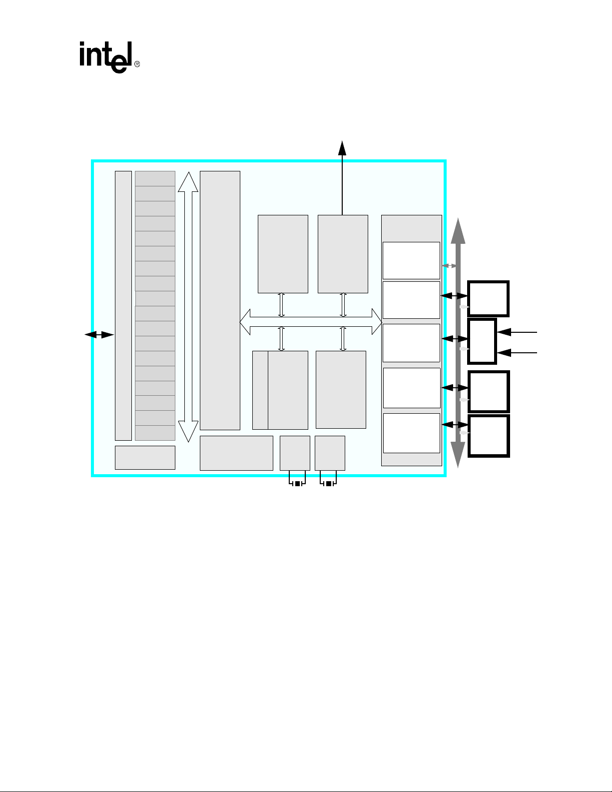
Figure 1-1. PXA27x Processor Block Diagram
RTC
OS Timers
4 x PWM
Interrupt C
3 x SSP
USIM
I2S
AC97
Full Function
Uart
Bluetooth
Uart
Fast IrDA
Slow IrDA
I2C
USB
Client
General Purpose I/O
Baseband
Interface
Keypad
Interface
SDcard/MMC
Interface
Mem Stick
Interface
Primary GPIO
DMA
Controller
And
Peripheral Bus
Bridge
Power Management
Clock Control
Internal
Intel® Wireless
MMX™ Technology
SRAM
System Bus
Intel
XScale®
Core
13
MHz
Osc
LCD
LCD
Controller
USB
HOST
32.768
KHz
Osc
Memory
Controller
Address
and
Data
Variabl e
Latency I/O
Control
PCMCIA & CF
Control
Dynamic
Memory
Control
Stati c
Memory
Control
Introduction
Address and Data
ASIC
XCVR
SDRAM/
SMROM
4 banks
ROM/
Flash/
SRAM
4 Banks
Socket 0
Socket 1
1.2.1 Intel XScale® Microarchitecture and Intel XScale® core
The Intel XScale® Microarchitecture is based on a core that is ARM* version 5TE compliant. The
microarchitecture surrounds the core with instruction and data memory management units;
instruction, data, and mini-data caches; write, fill, pend, and branch-target buffers; power
management, performance monitoring, debug, and JTAG units; coprocessor interface; 32K caches;
MMUs; BTB; MAC coprocessor; and core memory bus.
The Intel XScale® Microarchitecture can be combined with peripherals to provide applicationspecific standard products (ASSPs) targeted at selected market segments. For example, the RISC
core can be integrated with peripherals such as an LCD controller, multimedia controllers, and an
external memory interface to empower OEMs to develop smaller, more cost-effective handheld
devices with long battery life, with the performance to run rich multimedia applications. Or the
microarchitecture could be surrounded by high-bandwidth PCI interfaces, memory controllers, and
networking micro-engines to provide a highly integrated, low-power, I/O or network processor.
Intel® PXA27x Processor Family Optimization Guide 1-3
Page 14

Introduction
1.2.2 Intel XScale® Microarchitecture Features
• Superpipelined RISC technology achieves high speed and low power
• Wireless Intel Speedstep® technology allows on-the-fly voltage and frequency scaling to
enable applications to use the right blend of performance and power
• Media processing technology enables the MAC coprocessor perform two simultaneous 16-bit
SIMD multiplies with 64-bit accumulation for efficient media processing
• Power management unit provides power savings via multiple low-power modes
• 128-entry Branch Target buffer keeps pipeline filled with statistically correct branch choices
• 32-Kbyte instruction cache (I-cache) keeps local copy of important instructions to enable high
performance and low power
• 32-Kbyte data cache (D-cache) keeps local copy of important data to enable high performance
and low power
• 2-Kbyte mini-data cache avoids “thrashing” of the D-cache for frequently changing data
streams
• 32-entry instruction memory management unit enables logical-to-physical address translation,
access permissions, I-cache attributes
• 32-entry data memory management unit enables logical-to-physical address translation, access
permissions, D-cache attributes
• 4-entry Fill and Pend buffers promote core efficiency by allowing “hit-under-miss” operation
with data caches
• Performance monitoring unit furnishes two 32-bit event counters and one 32-bit cycle counter
for analysis of hit rates
• Debug unit uses hardware breakpoints and 256-entry Trace History buffer (for flow change
messages) to debug programs
• 32-bit coprocessor interface provides high performance interface between core and
coprocessors
• 8-entry Write buffer allows the core to continue execution while data is written to memory
See the Intel XScale® Microarchitecture Users Guide for additional information.
1.2.3 Intel® Wireless MMX™ technology
The Intel XScale® Microarchitecture has attached to it a coprocessor to accelerate multimedia
applications. This coprocessor, characterized by a 64-bit Single Instruction Multiple Data (SIMD)
architecture and compatibility with the integer functionality of the
technology
technology
and SSE instruction sets, is known by its Intel project name, Intel® Wireless MMX™
. The key features of this coprocessor are:
• 30 new media processing instructions
• 64-bit architecture up to eight-way SIMD
• 16 x 64-bit register file
• SIMD PSR flags with group conditional execution support
• Instruction support for SIMD, SAD, and MAC
• Instruction support for alignment and video
• Intel® Wireless MMX™ technology and SSE integer compatibility
1-4 Intel® PXA27x Processor Family Optimization Guide
Intel® Wireless MMX™
Page 15

• Superset of existing Intel XScale® Microarchitecture media processing instructions
See the Intel® Wireless MMX™ technology Coprocessor EAS for more details.
1.2.4 Memory Architecture
1.2.4.1 Caches
There are two caches:
• Data cache – The PXA27x processor supports 32 Kbytes of data cache.
• Instruction Cache – The PXA27x processor supports 32 Kbytes of instruction cache.
1.2.4.2 Internal Memories
The key features of the PXA27x processor internal memory are:
• 256 Kbytes of on-chip SRAM arranged as four banks of 64 Kbytes
• Bank-by-bank power management with automatic power management for reduced power
consumption
• Byte write support
Introduction
1.2.4.3 External Memory Controller
The PXA27x processor supports a memory controller for external memory which can access:
• SDRAM up to 100 MHz at 1.8 Volts.
• Flash memories
• Synchronous ROM
• SRAM
• Variable latency input/output (VLIO) memory
• PC card and compact flash expansion memory
1.2.5 Processor Internal Communications
The PXA27x processor supports a hierarchical bus architecture. A system bus supports high
bandwidth peripherals, and a slower peripheral bus supports peripherals with lower data
throughputs.
1.2.5.1 System Bus
• Interconnection between the major key components is through the system bus.
• 64-bit wide, address and data multiplexed bus.
• The system bus allows split transactions, increasing the maximum data-throughput in the
system.
• Different burst sizes are allowed; up to 4 data phases per transactions (that is, 32 bytes). The
burst size is set in silicon for each peripheral and is not configurable.
Intel® PXA27x Processor Family Optimization Guide 1-5
Page 16

Introduction
• The system bus can operate at different frequency ratios with respect to the Intel XScale® core
(up to 208 MHz). The frequency control of the system bus is pivotal to striking a balance
between the desired performance and power consumption.
1.2.5.2 Peripheral Bus
The peripheral bus is a single master bus. The bus master arbitrates between the Intel XScale® core
and the DMA controller with a pre-defined priority scheme between them. The peripheral bus is
used by the low-bandwidth peripherals; the peripheral bus runs at 26
1.2.5.3 Peripherals in the Processor
The PXA27x processor has a rich set of peripherals. The list of peripherals and key features are
described in the subsections below.
1.2.5.3.1 LCD Display Controller
The LCD controller supports single- or dual-panel LCD displays. Color panels without internal
frame buffers up to 262144 colors (18
up to 16777216 colors (24
(8
bits) are supported.
bits) are supported. Monochrome panels up to 256 gray-scale levels
bits) are supported. Color panels with internal frame buffers
MHz.
1.2.5.3.2 DMA Controller
The PXA27x processor has a high performance DMA controller supporting memory-to-memory
transfers, peripheral-to-memory and memory-to-peripheral device transfers. It has support for
32
channels and up to 63-peripheral devices. The controller can perform descriptor chaining. DMA
supports descriptor-fetch, no-descriptor-fetch and descriptor-chaining.
1.2.5.3.3 Other Peripherals
The PXA27x processor offers this peripheral support:
• USB Client Controller with 23 programmable endpoints (compliant with USB Revision 1.1).
• USB Host controller (USB Rev. 1.1 compatible), which supports both low-speed and full-
speed USB devices through a built-in DMA controller.
• Intel® Quick Capture Interface which provides a connection between the processor and a
camera image sensor.
• Infrared Communication Port (ICP) which supports 4 Mbps data rate compliant with Infrared
Data Association (IrDA) standard.
2
• I
C Serial Bus Port, which is compliant with I2C standard (also supports arbitration between
multiple-masters).
• AC97 CODEC Interface (compliant with AC97 2.0) supporting multiple independent channels
(different channels are used for stereo PCM In, stereo PCM Out, MODEM Out, MODEM-In
and mono Mic-in).
2
• I
S Audio CODEC Interface.
• Three flexible synchronous serial ports.
• Multimedia Card Controller supports the MMC, SD and SDIO protocols.
• The PXA27x processor supports three UARTs compatible with 16550 and 16750 standard.
1-6 Intel® PXA27x Processor Family Optimization Guide
Page 17

Introduction
• Memory Stick Host Controller - compliant with Memory Stick V1.3 standard.
• USIM card interface (compliant with ISO standard 7816-3 and 3G TS 31.101)
• MSL – the physical interface of communication subsystems for mobile or wireless platforms.
The operating system and application software uses this to communicate between each other.
• Keypad interface supports both direct key as well as matrix key.
• Real-time clock (RTC) controller which provides a general-purpose, real-time reference clock
for use by the system.
• The pulse width modulator (PWM) controller generates four independent PWM outputs.
• Interrupt controller identifiesand controls the interrupt sources available to the processor.
• The OS timers controller provides a set of timer channels that allow software to generate timed
interrupts or wake-up events.
• General-purpose I/O (GPIO) controller for use in generating and capturing application-
specific input and output signals. Each of the 121
an input (or as bidirectional for certain alternate functions).
1
GPIOs may be programmed as an output,
1.2.6 Wireless Intel Speedstep® technology
Wireless Intel Speedstep® technology advances the capabilities of Intel® Dynamic Voltage
Management - a function already built into the Intel XScale® Microarchitecture - by incorporating
three new low-power states: deep idle, standby and deep sleep. The technology is able to change
both voltage and frequency on-the-fly by intelligently switching the processor into the various low
power modes, saving additional power while still providing the necessary performance to run rich
applications.
The PXA27x processor integrated microprocessor provides a rich set of flexible powermanagement controls for a wide range of usage models, while enabling very low-power operation.
The key features include:
• Five reset sources:
—Power-on
— Hardware
— Watchdog
—GPIO
— Exit from sleep mode
• Three clock-speed controls to adjust frequency:
— Turbo mode
— Divisor mode
—Fast Bus mode
• Switchable clock source
• Functional clock gating
• Programmable frequency-change capability
1. 121 GPIOs are available on the PXA271 processor, PXA271 processor, and PXA271 processor. The PXA270 processor only has 119 GPIOs
bonded out.
Intel® PXA27x Processor Family Optimization Guide 1-7
Page 18

Introduction
• Six power modes to control power consumption:
—Normal
—Idle
— Deep idle
— Standby
— Sleep
— Deep sleep
• Programmable I
See the Intel® PXA27x Processor Family Developer’s Manual for more details.
2
C-based external regulator interface to support voltage changing.
1.3 Intel XScale® Microarchitecture Compatibility
The Intel XScale® Microarchitecture is ARM*Version 5 (V5TE) architecture compliant. The
PXA27x processor implements the integer instruction set architecture of ARM*V5TE.
Backward compatibility for user-mode applications is maintained with the earlier generations of
StrongARM* and Intel XScale® Microarchitecture processors. Operating systems may require
modifications to match the specific Intel XScale® Microarchitecture hardware features, and to take
advantage of the performance enhancements added to this core.
Memory map and register locations are backward-compatible with the previous Intel XScale®
Microarchitecture hand-held products.
The Intel® Wireless MMX™ technology instruction set is compatible with the standard ARM*
coprocessor instruction format (See
for more details).
The Complete Guide to Intel® Wireless MMX™ Technology
1.3.1 PXA27x Processor Performance Features
Performance features of the PXA27x processor are:
• 32-Kbyte instruction cache
• 32-Kbyte data cache
• Intel® Wireless MMX™ technology with sixteen 64-bit registers, optimized instructions for
video, and multi-media applications.
• The PXA27x processor has an internal SRAM of 256 KBytes.
• Capability of locking entries in the instruction or data caches
• 2-Kbyte mini-data cache, separate from the data cache
• L1 caches and the mini-data cache use virtual address indices (or tags)
• Separate instruction and data Translation Lookaside buffers (TLBs), each with 32 entries
• Capability of locking entries in the TLBs
• 16-channel DMA engine with transfer-size control and descriptor chaining
1-8 Intel® PXA27x Processor Family Optimization Guide
Page 19

Introduction
• PID register for fast virtual address remapping
• Vect o r r emap
• Interrupt controller offers faster interrupt latency with the help of programmable priority
sorting mechanism.
• Extensions to the exception model to include imprecise data and instruction preload aborts
• Access control to other coprocessors
• Enhanced set of supported cache-control options
• A branch target buffer for dynamic-branch prediction
• Performance monitoring unit
• Software-debug support, including instruction and data breakpoints, a serial debug link via the
JTAG interface and a 256-entry trace buffer
• Integrated memory controller with support for SDRAM, flash memory, synchronous ROM,
SRAM, variable latency I/O (VLIO) memory, PC card, and compact flash expansion memory.
• Six power-management modes
Intel® PXA27x Processor Family Optimization Guide 1-9
Page 20

Introduction
1-10 Intel® PXA27x Processor Family Optimization Guide
Page 21
Microarchitecture Overview 2
2.1 Introduction
This chapter contains an overview of Intel XScale® Microarchitecture and Intel® Wireless
MMX™ Technology
architecture with an enhanced memory pipeline. The Intel XScale® Microarchitecture instruction
set is based on ARM* V5TE architecture; however, the Intel XScale® Microarchitecture includes
new instructions. Code developed for the Intel® StrongARM* SA-110 (SA-110), Intel®
StrongARM* SA-1100 (SA-1100), and Intel® StrongARM* SA-1110 (SA-1110) microprocessors
is portable to Intel XScale® Microarchitecture based processors. However, to obtain the maximum
performance, the code should be optimized for the Intel XScale® Microarchitecture using the
techniques presented in this document.
2.2 Intel XScale® Microarchitecture Pipeline
This section provides a brief description of the structure and behavior of Intel XScale®
Microarchitecture pipeline.
2.2.1 General Pipeline Characteristics
. The Intel XScale® Microarchitecture includes a superpipelined RISC
The following sections discuss general pipeline characteristics.
2.2.1.1 Pipeline Organization
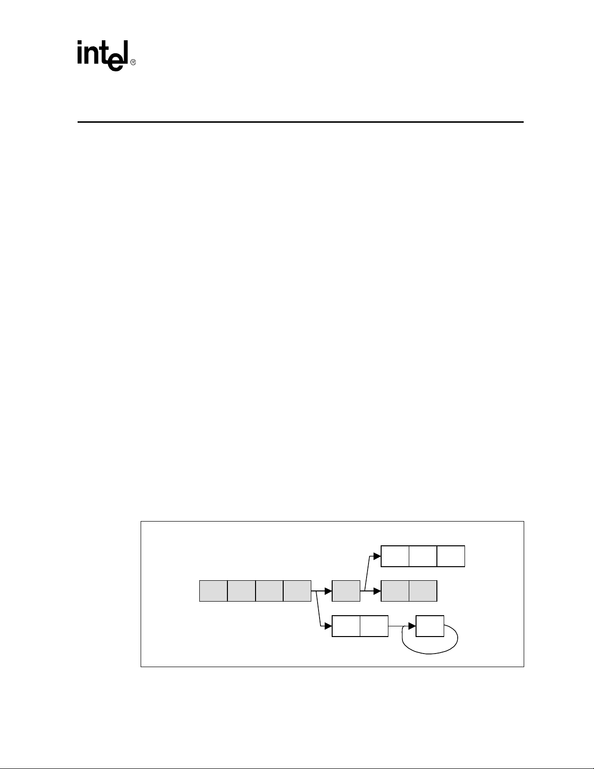
The Intel XScale® Microarchitecture has a 7-stage pipeline operating at a higher frequency than its
predecessors allowing for greater overall performance. The Intel XScale® Microarchitecture
single-issue superpipeline consists of a main execution pipeline, a multiply-accumulate {MAC}
pipeline, and a memory access pipeline.
execution pipeline shaded.
Figure 2-1. Intel XScale® Microarchitecture RISC Superpipeline
Main execution pipeline
F1 F2 ID RF X1 X2
Figure 2-1 shows the pipeline organization with the main
MAC pipeline
M1 M2 Mx
Memory pipeline
D1 D2
XWB
DWB
Intel® PXA27x Processor Family Optimization Guide 2-1
Page 22

Microarchitecture Overview
Tab le 2-1 gives a brief description of each pipe stage and a reference for further information.
Table 2-1. Pipelines and Pipe Stages
Pipe / Pipestage Description For More Information
Main Execution Pipeline
• IF1/IF2
•ID
•RF
•X1
•X2
•XWB
Memory Pipeline
•D1/D2
•DWB
MAC Pipeline
•M1-M5
• MWB (not shown)
Handles data processing instructions
Instruction Fetch
Instruction Decode
Register File / Operand Shifter
ALU Execute
State Execute
Write-back
Handles load/store instructions
Data cache access
Data cache writeback
Handles all multiply instructions
Multiplier stages
MAC write-back occurs during M2-M5
2.2.1.2 Out of Order Completion
While the pipeline is scalar and single-issue, instructions occupy all three pipelines at once. The
main execution pipeline, memory, and MAC pipelines have different execution times because they
are not lock-stepped. Sequential consistency of instruction execution relates to two aspects: first,
the order instructions are completed and second, the order memory is accessed due to load and
store instructions. The Intel XScale® Microarchitecture only preserves a weak processor
consistency because instructions complete out of order (assuming no data dependencies exist).
The Intel XScale® Microarchitecture can buffer up to four outstanding reads. If load operations
miss the data cache, subsequent instructions complete independently. This operation is called a
hit-under-miss operation.
Section 2.2.3
Section 2.2.3.1
Section 2.2.3.2
Section 2.2.3.3
Section 2.2.3.4
Section 2.2.3.5
Section 2.2.3.6
Section 2.2.4
Section 2.2.4.1
Section 2.2.5.1
Section 2.2.5
Section 2.2.5
Section 2.2.5
2.2.1.3 Use of Bypassing
The pipeline makes extensive use of bypassing to minimize data hazards. To eliminate the need to
stall the pipeline, bypassing allows results forwarding from multiple sources.
In certain situations, the pipeline must stall because of register dependencies between instructions.
A register dependency occurs when a previous MAC or load instruction is about to modify a
register value that has not returned to the register file. Core bypassing allows the current instruction
to execute when the previous instruction’s results are available without waiting for the register file
to update.
2.2.2 Instruction Flow Through the Pipeline
With the exception of the MAC unit, the pipeline issues one instruction per clock cycle. Instruction
execution begins at the F1 pipestage and completes at the WB pipestage.
Although a single instruction is issued per clock cycle, all three pipelines are processing
instructions simultaneously. If there are no data hazards, each instruction complete independently
of the others.
2-2 Intel® PXA27x Processor Family Optimization Guide
Page 23

2.2.2.1 ARM* V5TE Instruction Execution
Figure 2-1 uses arrows to show the possible flow of instructions in the pipeline. Instruction
execution flows from the F1 pipestage to the RF pipestage. The RF pipestage issues a single
instruction to either the X1 pipestage or the MAC unit (multiply instructions go to the MAC, while
all others continue to X1). This means that M1 or X1 are idle.
After calculating the effective addresses in XI, all load and store instructions route to the memory
pipeline.
The ARM* V5TE branch and exchange (BX) instruction (used to branch between ARM* and
THUMB* code) causes the entire pipeline to be flushed. If the processor is in THUMB* mode the
ID pipestage dynamically expands each THUMB* instruction into a normal ARM* V5TE RISC
instruction and normal execution resumes.
2.2.2.2 Pipeline Stalls
Pipeline stalls can seriously degrade performance. The primary reasons for stalls are register
dependencies, load dependencies, multiple-cycle instruction latency, and unpredictable branches.
To help maximize performance, it is important to understand some of the ways to avoid pipeline
stalls. The following sections provide more detail on the nature of the pipeline and ways of
preventing stalls.
Microarchitecture Overview
2.2.3 Main Execution Pipeline
2.2.3.1 F1 / F2 (Instruction Fetch) Pipestages
The job of the instruction fetch stages F1 and F2 is to present the next instruction to be executed to
the ID stage. Two important functional units residing within the F1 and F2 stages are the BTB and
IFU.
• Branch Target Buffer (BTB)
The BTB provides a 128-entry dynamic branch prediction buffer. An entry in the BTB is
created when a B or BL instruction branch is taken for the first time. On sequential executions
of the branch instruction at the same address, the next instruction loaded into the pipeline is
predicted by the BTB. Once the branch type instruction reaches the X1 pipestage, its target
address is known. Execution continues without stalling if the target address is the same as the
BTB predicted address. If the address is different from the address that the BTB predicted, the
pipeline is flushed, execution starts at the new target address, and the branch’s history is
updated in the BTB.
• Instruction Fetch Unit (IFU)
The IFU is responsible for delivering instructions to the instruction decode (ID) pipestage. It
delivers one instruction word each cycle (if possible) to the ID. The instruction could come
from one of two sources: instruction cache or fetch buffers.
Intel® PXA27x Processor Family Optimization Guide 2-3
Page 24

Microarchitecture Overview
2.2.3.2 Instruction Decode (ID) Pipestage
The ID pipestage accepts an instruction word from the IFU and sends register decode information
to the RF pipestage. The ID is able to accept a new instruction word from the IFU on every clock
cycle in which there is no stall. The ID pipestage is responsible for:
• General instruction decoding (extracting the opcode, operand addresses, destination addresses
and the offset).
• Detecting undefined instructions and generating an exception.
• Dynamic expansion of complex instructions into sequence of simple instructions. Complex
instructions are defined as ones that take more than one clock cycle to issue, such as LDM,
STM, and SWP.
2.2.3.3 Register File / Shifter (RF) Pipestage
The main function of the RF pipestage is to read and write to the register file unit (RFU). It
provides source data to:
• X1 for ALU operations
• MAC for multiply operations
• Data cache for memory writes
• Coprocessor interface
The ID unit decodes the instruction and specifies the registers accessed in the RFU. Based on this
information, the RFU determines if it needs to stall the pipeline due to a register dependency. A
register dependency occurs when a previous instruction is about to modify a register value that has
not been returned to the RFU and the current instruction needs to access that same register. If no
dependencies exist, the RFU selects the appropriate data from the register file and passes it to the
next pipestage. When a register dependency does exist, the RFU keeps track of the unavailable
register. The RFU stops stalling the pipe when the result is returned.
The ARM* architecture specifies one of the operands for data processing instructions as the shifter
operand. A 32-bit shift can be performed on a value before it is used as an input to the ALU. This
shifter is located in the second half of the RF pipestage.
2.2.3.4 Execute (X1) Pipestages
The X1 pipestage performs these functions:
• ALU calculations – the ALU performs arithmetic and logic operations, as required for data
processing instructions and load/store index calculations.
• Determine conditional instruction executions – the instruction’s condition is compared to the
CPSR prior to execution of each instruction. Any instruction with a false condition is
cancelled and does not cause any architectural state changes, including modifications of
registers, memory, and PSR.
• Branch target determinations – the X1 pipestage flushes all instructions in the previous
pipestages and sends the branch target address to the BTB if a branch is mispredicted by the
BTB. The flushing of these instructions restarts the pipeline.
2-4 Intel® PXA27x Processor Family Optimization Guide
Page 25

2.2.3.5 Execute 2 (X2) Pipestage
The X2 pipestage contains the program status registers (PSR). This pipestage selects the data to be
written to the RFU in the WB cycle including the following items.
The X2 pipestage contains the current program status register (CPSR). This pipestage selects what
is written to the RFU in the WB cycle including program status registers.
2.2.3.6 Write-Back (WB)
When an instruction reaches the write-back stage it is considered complete. Instruction results are
written to the RFU.
2.2.4 Memory Pipeline
The memory pipeline consists of two stages, D1 and D2. The data cache unit (DCU) consists of the
data cache array, mini-data cache, fill buffers, and write buffers. The memory pipeline handles load
and store instructions.
2.2.4.1 D1 and D2 Pipestage
Microarchitecture Overview
Operation begins in D1 after the X1 pipestage calculates the effective address for loads and stores.
The data cache and mini-data cache return the destination data in the D2 pipestage. Before data is
returned in the D2 pipestage, sign extension and byte alignment occurs for byte and half-word
loads.
2.2.4.1.1 Write Buffer Behavior
The Intel XScale® Microarchitecture has enhanced write performance by the use of write
coalescing. Coalescing is combining a new store operation with an existing store operation already
resident in the write buffer. The new store is placed in the same write buffer entry as an existing
store when the address of new store falls in the 4-word aligned address of the existing entry.
The core can coalesce any of the four entries in the write buffer. The Intel XScale®
Microarchitecture has a global coalesce disable bit located in the Control register (CP15, register 1,
opcode_2=1).
2.2.4.1.2 Read Buffer Behavior
The Intel XScale® Microarchitecture has four fill buffers that allow four outstanding loads to the
cache and external memory. Four outstanding loads increases the memory throughput and the bus
efficiency. This feature can also be used to hide latency. Page table attributes affect the load
behavior; for a section with C=0, B=0 there is only one outstanding load from the memory. Thus,
the load performance for a memory page with C=0, B=1 is significantly better compared to a
memory page with C=0, B=0.
2.2.5 Multiply/Multiply Accumulate (MAC) Pipeline
The multiply-accumulate (MAC) unit executes the multiply and multiply-accumulate instructions
supported by the Intel XScale® Microarchitecture. The MAC implements the 40-bit Intel XScale®
Microarchitecture accumulator register acc0 and handles the instructions which transfers its value
to and from general-purpose ARM* registers.
Intel® PXA27x Processor Family Optimization Guide 2-5
Page 26

Microarchitecture Overview
These are important characteristics about the MAC:
• The MAC is not a true pipeline. The processing of a single instruction requires use of the same
data-path resources for several cycles before a new instruction is accepted. The type of
instruction and source arguments determine the number of required cycles.
• No more than two instructions can concurrently occupy the MAC pipeline.
• When the MAC is processing an instruction, another instruction cannot enter M1 unless the
original instruction completes in the next cycle.
• The MAC unit can operate on 16-bit packed signed data. This reduces register pressure and
memory traffic size. Two 16-bit data items can be loaded into a register with one LDR.
• The MAC can achieve throughput of one multiply per cycle when performing a 16-by-32-bit
multiply.
• ACC registers in the Intel XScale® Microarchitecture can be up to 64 bits in future
implementations. Code should be written to depend on the 40-bit nature of the current
implementation.
2.2.5.1 Behavioral Description
The execution of the MAC unit starts at the beginning of the M1 pipestage. At this point, the MAC
unit receives two 32-bit source operands. Results are completed N cycles later (where N is
dependent on the operand size) and returned to the register file. For more information on MAC
instruction latencies, refer to
Microarchitecture”.
Section 4.8, “Instruction Latencies for Intel XScale®
An instruction occupying the M1 or M2 pipestages occupies the X1 and X2 pipestage, respectively.
Each cycle, a MAC operation progresses for M1 to M5. A MAC operation may complete anywhere
from M2-M5.
2.2.5.2 Perils of Superpipelining
The longer pipeline has several consequences worth considering:
• Larger branch misprediction penalty (four cycles in the Intel XScale® Microarchitecture
instead of one in StrongARM* Architecture).
• Larger load use delay (LUD) — LUDs arise from load-use dependencies. A load-use
dependency gives rise to a LUD if the result of the load instruction cannot be made available
by the pipeline in time for the subsequent instruction. To avoid these penalties, an optimizing
compiler should take advantage of the core’s multiple outstanding load capability (also called
hit-under-miss) as well as finding independent instructions to fill the slot following the load.
• Certain instructions incur a few extra cycles of delay with the Intel XScale® Microarchitecture
as compared to StrongARM* processors (LDM, STM).
• Decode and register file lookups are spread out over two cycles with the Intel XScale®
Microarchitecture, instead of one cycle in predecessors.
2-6 Intel® PXA27x Processor Family Optimization Guide
Page 27
Microarchitecture Overview
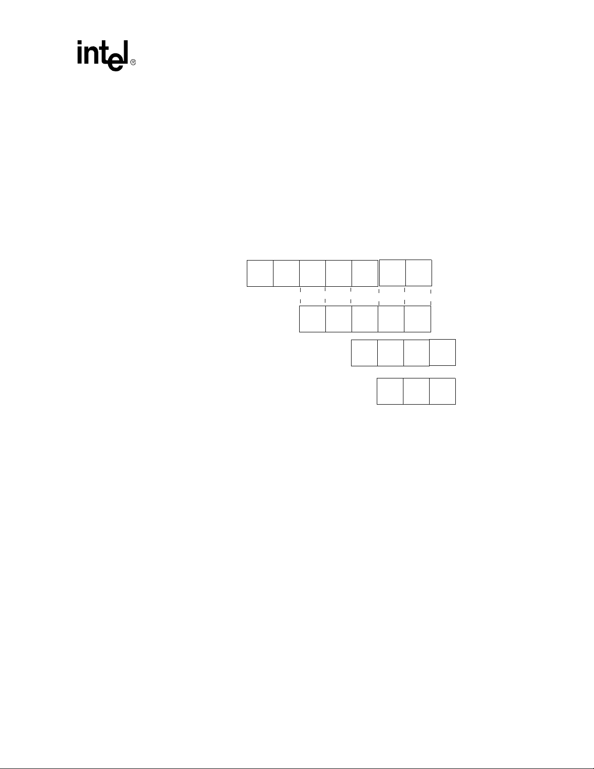
2.3 Intel® Wireless MMX™ Technology Pipeline
As the Intel® Wireless MMX™ Technology is tightly coupled with the Intel XScale®
Microarchitecture; the
structure as the Intel XScale® Microarchitecture.
Technology pipeline, which contains three independent pipeline threads:
• X pipeline - Execution pipe
• M pipeline - Multiply pipe
• D pipeline - Memory pipe
Figure 2-2. Intel® Wireless MMX™ Technology Pipeline Threads and relation with Intel
XScale® Microarchitecture Pipeline
Intel® Wireless MMX™ Technology pipeline follows the similar pipeline
Figure 2-2 shows the Intel® Wireless MMX™
Intel
XScale®
Pipeline
IF1 IF2
ID
RF
X1
X2 XWB
X pipeline
M pipeline
D pipeline
2.3.1 Execute Pipeline Thread
2.3.1.1 ID Stage
The ID pipe stage is where decoding of Intel® Wireless MMX™ Technology instructions
commences. Because of the significance of the transit time from Intel XScale® Microarchitecture
in the ID pipe stage, only group decoding is performed in the ID stage, with the remainder of the
decoding being completed in the RF stage. However, it is worth noting that the register address
decoding is fully completed in the ID stage because the register file needs to be accessed at the
beginning of the RF stage.
All instructions are issued in a single cycle, and they pass through the ID stage in one cycle if no
pipeline stall occurs.
2.3.1.2 RF Stage
ID
RF X1
M1
X2 XWB
M2
D1 D2 DWB
MWBM3
The RF stage controls the reading/writing of the register file, and determines if the pipeline has to
stall due to data or resource hazards. Instruction decoding also continues at the RF stage and
completes at the end of the RF stage. The register file is accessed for reads in the high phase of the
clock and accessed for writes in the low phase.If data or resource hazards are detected, the
Intel® PXA27x Processor Family Optimization Guide 2-7
Intel®
Page 28

Microarchitecture Overview
Wireless MMX™ Technology stalls Intel XScale® Microarchitecture. Note that control hazards
are detected in the Intel XScale® Microarchitecture, and a flush signal is sent from the core to the
Intel® Wireless MMX™ Technology.
2.3.1.3 X1 Stage
The X1 stage is also known as the execution stage, which is where most instructions begin being
executed. All instructions are conditionally executed and that determination occurs at the X1 stage
in the Intel XScale® Microarchitecture. A signal from the core is required to indicate whether the
instruction being executed is committed. In other words, an instruction being executed at the X1
stage may be canceled by a signal from the core. This signal is available to the
MMX™ Technology
2.3.1.4 X2 Stage
The Intel® Wireless MMX™ Technology supports saturated arithmetic operations. Saturation
detection is completed in the X2 pipe stage.
If the Intel XScale® Microarchitecture detects exceptions and flushes in the X2 pipe stage, Intel®
Wireless MMX™ Technology
Intel® Wireless
in the middle of the X1 pipe stage.
also flushes all the pipeline stages.
2.3.1.5 XWB Stage
The XWB stage is the last stage of the X pipeline, where a final result calculated in the X pipeline
is written back to the register file.
2.3.2 Multiply Pipeline Thread
2.3.2.1 M1 Stage
The M pipeline is separated from the X pipeline. The execution of multiply instructions starts at the
beginning of the M1 stage, which aligns with the X1 stage of the X pipeline. While the issue cycle
for multiply operations is one clock cycle, the result latency is at least three cycles. Certain
instructions such as TMIA, WMAC, WMUL, WMADD spend two M1 cycles since the
Wireless MMX™ Technology
level compression occur in the M1 pipe stage.
2.3.2.2 M2 Stage
Additional compression occurs in the M2 pipe stage, and the lower 32 bits of the result are
calculated with a 32 bit adder.
2.3.2.3 M3 Stage
The upper 32 bits of the result are calculated with a 32-bit adder.
has only two 16x16 multiplier arrays. Booth encoding and first-
Intel®
2.3.2.4 MWB Stage
The MWB stage is the last stage of the M pipeline, which is where a final result calculated in the M
pipeline is written back to the register file.
2-8 Intel® PXA27x Processor Family Optimization Guide
Page 29

A forwarding path from the MWB stage to the RF stage serves as a non-critical bypass. Critical and
reasonable logic insertion are allowed.
2.3.3 Memory Pipeline Thread
2.3.3.1 D1 Stage
In the D1 pipe stage, the Intel XScale® Microarchitecture provides a virtual address that is used to
access the data cache. There is no logic inside the
pipe stage.
2.3.3.2 D2 Stage
The D2 stage is where load data is returned. Load data comes from either data cache or external
memory, with external memory having the highest priority. The
Technology
2.3.3.3 DWB Stage
needs to bridge incoming 32-bit data to internal 64-bit data.
Microarchitecture Overview
Intel® Wireless MMX™ Technology in the D1
Intel® Wireless MMX™
The DWB stage—the last stage of the D pipeline—is where load data is written back to the register
file.
Intel® PXA27x Processor Family Optimization Guide 2-9
Page 30

Microarchitecture Overview
2-10 Intel® PXA27x Processor Family Optimization Guide
Page 31

System Level Optimization 3
This chapter describes relevant performance considerations that developers and system designers
should be aware of to efficiently use the Intel® PXA27x Processor Family (PXA27x processor).
3.1 Optimizing Frequency Selection
The PXA27x processor offers a range of combinations of core, system bus and memory clock
speed. The run mode frequency and derived system bus and memory controller frequencies affect
the latency and throughput of external memory interfaces.
Memory latencies depend on the run mode frequency, because a higher run mode frequency
improves performance for memory bound applications. The core clock speed is indicated by the
run frequency, or (if CLKCFG[T] is set) by the turbo frequency. This value is most significant for
computationally bound applications. For a memory bound application, a processor operating in
333-MHz run mode might perform better than a processor operating in 400-MHz turbo mode using
only a 200-MHz run mode frequency. The clock frequency combination should be chosen to fit the
target application mix. Possible frequency selections are listed in the clocks and power manager
section of the Intel® PXA27x Processor Family Developer’s Manual.
3.2 Memory System Optimization
3.2.1 Optimal Setting for Memory Latency and Bandwidth
Because the PXA27x processor has a multi-transactional internal bus, there are latencies involved
with accesses to and from the Intel XScale® core. The internal bus, also called the system bus,
allows many internal operations to occur concurrently such as LCD, DMA controller and related
data transfers.
frequencies. The throughput reported in the tables is only measuring load
Table 3-1. External SDRAM Access Latency and Throughput for Different Frequencies
(Silicon Measurement Pending)
Core Clock
Speed (MHz)
(up to)
104 104 104 104 17 205
208 208 208 104 21 326
312 208 208 104 30 343
Tab le 3-1 and Tabl e 3-2 list latencies and throughputs associated with different
Run Mode
Frequency (MHz)
(up to)
System Bus Clock
Speed (MHz)
(up to)
Memory
Clock Speed
(MHz)
(up to)
Memory
Latency
(core cycles)
Load
Throughput
from Memory
(MBytes/
Sec)
Intel® PXA27x Processor Family Optimization Guide 3-1
Page 32

System Level Optimization
Table 3-2. Internal SRAM Access Latency and Throughput for Different Frequencies (Silicon
Measurement Pending)
Core Clock
Speed (MHz)
(up to)
104 104 104 104 14 236
208 208 208 104 14 472
312 208 208 104 21 473
Store throughput is similar
†
Run Mode
Frequency (MHz)
(up to)
System Bus Clock
Speed (MHz)
(up to)
Memory
Clock Speed
(MHz)
(up to)
Memory
Latency
(core cycles)
Throughput
from Memory
(MBytes/
• Setting wait-states for static memory
For static memory, it is important to use the correct number of wait-states to get optimal
performance. The Intel® PXA27x Processor Family Developer’s Manual explains the
possible values in the MSCx registers. These registers control wait states and set up the access
mode used. For flash memory that supports burst-of-four reads or burst-of-eight reads, these
modes provide improvements in reading and executing from flash.
• CAS latency for SDRAM
For SDRAM the key parameter is the CAS latency. Lower CAS latency gives higher
performance. Most current SDRAM supports a CAS latency of two
• Setting of the APD bit
Use of the APD bit in the memory controller can save power, however can also increase the
memory latency. For high performance the APD bit should be cleared.
Load
Sec)
†
• Buffer Strength registers
The output drivers for the PXA27x processor external memory bus have programmable
strength settings. This feature allows for simple, software-based control of the output driver
impedance for the external memory bus. Use these registers to match the driver strength of the
PXA27x processor to external memory bus. The buffer strength should be set to the lowest
possible setting (minimum drive strength) that still allows for reliable memory system
performance. This will minimize the power usage of the external memory bus, which is a
major component of total system power. Refer to the Programmable Output Buffer Strength
registers described in the Intel® PXA27x Processor Family Developer’s Manual, for more
information.
3.2.2 Alternate Memory Clock Setting
An alternate set of memory bus selections are available through the use of CCCR[A], refer to the
“CCCR Bit Definitions” table in the Intel® PXA27x Processor Family Developer’s Manual. When
this bit is set the memory clock speed is expanded to allow it to be set as high as 208
cleared the maximum memory clock speed is 130
If CCCR[A] is cleared, use the “Core PLL Output Frequencies for 13-MHz Crystal with CCCR[A]
= 0” table in the Intel® PXA27x Processor Family Developer’s Manual when making the clock
setting selections. If CCCR[A] is set, use the “Core PLL Output Frequencies for 13-MHz Crystal
MHz.
MHz. When
3-2 Intel® PXA27x Processor Family Optimization Guide
Page 33

With B=0 and CCCR[A] = 1” table and the “Core PLL Output Frequencies for 13 MHz Crystal
With B=1 and CCCR[A] = 1” table in the Intel® PXA27x Processor Family Developer’s Manual
instead.
3.2.3 Page Table Configuration
Three bits for each page are used to configure each memory page’s cache behavior. Different
values of X,C,B determine the caching, reading and writing, and buffering policies of the pages.
3.2.3.1 Page Attributes For Instructions
When examining these bits in a descriptor, the instruction cache only utilizes the C bit. If the C bit
is clear, the instruction cache considers a code fetch from that memory to be noncacheable, and will
not fill a cache entry. If the C bit is set, then fetches from the associated memory region is cached.
3.2.3.2 Page Attributes For Data Access
For data access, all three attributes are important. If the X bit for a descriptor is zero, the C and B
bits operate as defined by the ARM* architecture. This behavior is detailed in
System Level Optimization
Table 3-3.
If the X bit for a descriptor is one, the C and B bits behave differently, as shown in Tab le 3-4. The
load and store buffer behavior in Intel XScale® Microarchitecture is explained in Section 2.2.4.1.1,
“Write Buffer Behavior” and Section 2.2.4.1.2, “Read Buffer Behavior”
Table 3-3. Data Cache and Buffer Behavior when X = 0
C B Cacheable?
0 0 N N ——Stall until complete
0 1 N Y ——
1 0 Y Y Write-through Read Allocate
1 1 Y Y Write-back Read Allocate
† Normally, the processor continues executing after a data access if no dependency on that access is
encountered. With this setting, the processor stalls execution until the data access completes. This
guarantees to software that the data access has taken effect by the time execution of the data access
instruction completes. External data aborts from such accesses are imprecise.
Load Buffering
and Write
Coalescing?
Write Policy
Line Allocation
Policy
Table 3-4. Data Cache and Buffer Behavior when X = 1 (Sheet 1 of 2)
C B Cacheable?
0 0 — — — — Unpredictable -- do not use
0 1 N Y — —
Load Buffering
and Write
Coalescing?
Write Policy
Line Allocation
Policy
Notes
†
Notes
Writes will not coalesce into
†
buffers
Intel® PXA27x Processor Family Optimization Guide 3-3
Page 34

System Level Optimization
Table 3-4. Data Cache and Buffer Behavior when X = 1 (Sheet 2 of 2)
C B Cacheable?
1 0
1 1 Y Y Write-back
† Normally, "bufferable" writes can coalesce with previously buffered data in the same address range
†† Refer to Intel XScale® Core Developer’s Manual and the Intel® PXA27x Processor Family Developer’s
(Mini-data
cache)
Manual
for a description of this register.
Load Buffering
and Write
Coalescing?
———
Write Policy
Line Allocation
Policy
Read/Write
Allocate
Notes
Cache policy is determined by
MD field of Auxiliary Control
††
register
Note: The Intel XScale® Microarchitecture page-attributes are different than the Intel® StrongARM*
SA-1110 Microprocessor (SA-1110). The SA-1110 code may behave differently on PXA27x
processor systems due to page attribute differences. Table 3- 5 describes the differences in the
encoding of the C and B bits for data accesses. The main difference occurs when cacheable and
nonbufferable data is specified (C=1, B=0); the SA-1110 uses this encoding for the mini-data cache
while the Intel XScale® Microarchitecture uses this encoding to specify write-through caching.
Another difference is when C=0, B=1, where the Intel XScale® Microarchitecture coalesces stores
in the write buffer; the SA-1110 does not.
Table 3-5. Data Cache and Buffer operation comparison for Intel® SA-1110 and Intel XScale®
Microarchitecture, X=0
Encoding SA-1110 Function Intel XScale® Microarchitecture Function
C=1,B=1
C=1,B=0
C=0,B=1
C=0,B=0
Cacheable in data cache; store misses can
coalesce in write buffer
Cacheable in mini-data cache; store misses
can coalesce in write buffer
Noncacheable; no coalescing in write buffer,
but can wait in write buffer
Noncacheable; no coalescing in the write
buffer, SA-110 stalls until this transaction is
done
Cacheable in data cache, store misses can
coalesce in write buffer
Cacheable in data cache, with a write-through
policy. Store misses can coalesce in write
buffer
Noncacheable; stores can coalesce in the write
buffer
Noncacheable, no coalescing in the write
buffer, Intel XScale® Microarchitecture stalls
until the operation completes.
3.3 Optimizing for Instruction and Data Caches
Cache locking allows frequently used code to be locked in the cache. Up to 28 cache lines can be
locked in a set, while the remaining four entries still participate in the round robin replacement
policy.
3.3.1 Increasing Instruction Cache Performance
The performance of the PXA27x processor is highly dependent on the cache miss rate. Due to the
complexity of the processor fetching instructions from external memory can have a large latency.
Moreover, this cycle penalty becomes significant when the Intel XScale® core is running much
faster than external memory. Executing non-cached instructions severely curtails the processor's
performance so it is important to do everything possible to minimize cache misses.
3-4 Intel® PXA27x Processor Family Optimization Guide
Page 35

3.3.1.1 Round Robin Replacement Cache Policy
Both the data and the instruction caches use a round robin replacement policy to evict a cache line.
The simple consequence of this is that every line will eventually be evicted, assuming a non-trivial
program. The less obvious consequence is that predicting when and over which cache lines
evictions take place is difficult to predict. This information must be gained by experimentation
using performance profiling.
3.3.1.2 Code Placement to Reduce Cache Misses
Code placement can greatly affect cache misses. One way to view the cache is to think of it as 32
sets of 32 bytes, which span an address range of 1024 bytes. When running, the code maps into 32
blocks modular 1024 of cache space. Any overused sets will thrash the cache. The ideal situation is
for the software tools to distribute the code on a temporal evenness over this space.
This is not possible for a compiler to do automatically. Most of the input needed to best estimate
how to distribute the code will come from profiling followed by compiler-based two pass
optimizations.
3.3.1.3 Locking Code into the Instruction Cache
System Level Optimization
One important instruction cache feature is the ability to lock code into the instruction cache. Once
locked into the instruction cache, the code is always available for fast execution. Another reason
for locking critical code into cache is that with the round robin replacement policy, eventually the
code is evicted, even if it is a frequently executed function. Key code components to consider
locking are:
• Interrupt handlers
• OS Timer clock handlers
• OS critical code
• Time critical application code
The disadvantage to locking code into the cache is that it reduces the cache size for the rest of the
program. How much code to lock is application dependent and requires experimentation to
optimize.
Code placed into the instruction cache should be aligned on a 1024 byte boundary and placed
sequentially together as tightly as possible so as not to waste memory space. Making the code
sequential also insures even distribution across all cache ways. Though it is possible to choose
randomly located functions for cache locking, this approach runs the risk of locking multiple cache
ways in one set and few or none in another set. This distribution unevenness can lead to excessive
thrashing of instruction cache.
3.3.2 Increasing Data Cache Performance
There are different techniques which can be used to increase the data cache performance. These
include, optimizing cache configuration and programming techniques etc. This section offers a set
of system-level optimization opportunities; however program-level optimization techniques are
equally important.
Intel® PXA27x Processor Family Optimization Guide 3-5
Page 36

System Level Optimization
3.3.2.1 Cache Configuration
The Intel XScale® Microarchitecture allows users to define memory regions whose cache policies
can be set by the user. To support these various memory regions, OS configures the page-tables
accordingly.
The performance of application code depends on what cache policy used for data objects. A
description of when to use a particular policy is described below.
If the application is running under an OS, then the OS may restrict the application from using
certain cache policies.
3.3.2.1.1 Cache Configuration: Write-through and Write-back Cached Memory Regions
Write-back mode avoids some memory transactions by allowing data to collect in the data cache
before eventually being written to memory when the cache line is evicted. When cache lines are
evicted, the writes coalesce and are efficiently written to memory. This differs from write-through
mode where writes are always written to memory immediately. Write-through memory regions
generate more data traffic on the bus and consume more power due to increased bus activity. The
write-back policy is recommended to be used whenever possible. However, in a multi bus master
environment it may be necessary to use a write-through policy if data is shared across multiple
masters. In such a situation all shared memory regions should use write-through policy. Memory
regions that are private to a particular master should use the write-back policy.
3.3.2.1.2 Cache Configuration: Read Allocate and Read-write Allocate Memory Regions
Write-back with read/write allocate caches cause an additional read from the memory during a
write miss. Subsequent read and write performance may be improved by more frequent cache hits.
Most of the regular data and the stack for applications should be allocated to a read-write allocate
region. Data that is write only (or data that is written to and subsequently not used for a long time)
should be placed in a read allocate region. Under the read allocate policy, if a cache write miss
occurs, a new cache line is not allocated, and hence does not evict data from the data cache.
Memory intensive operations like a memcopy can actually be slowed down by the extra reads
required for the write allocate policy.
3.3.2.1.3 Cache Configuration: Noncacheable Regions
Noncachable memory regions (X=0, C=0, B=0) are frequently needed for I/O devices. For these
devices the relevant device registers and memory spaces are mapped as noncacheable. In some
cases making the noncacheable regions bufferable (X=0, C=0, and B =1) can accelerate the
memory performance due to write coalescing. There are cases where a noncached memory regions
must be set as nonbufferable (B=0):
• Any device where consecutive writes to the same address could be over-written in the write
buffer before reaching the target device (e.g. FIFOs).
• Devices where read/write order to the device is required. When coalescing occurs, writes
occur in numerical address order, not in the temporal order.
3.3.2.2 Creating Scratch RAM in the Internal SRAM
A very simple method for creating a fast scratch RAM is to allocate a portion of the Internal SRAM
for this purpose. This will allow data mapped to this area to be accessed much more quickly than if
it resided in external memory. Additionally, there are no considerations for cache locking, as are
discussed in the next section,
Section 3.3.2.3, “Creating Scratch RAM in Data Cache”.
3-6 Intel® PXA27x Processor Family Optimization Guide
Page 37

This is the preferred method for creating Scratch RAM for the PXA27x processor. It is generally
preferable to keep as much of the data cache as possible available for it’s designated use - cache
space. While access to the internal SRAM is slower than accessing data in cache, data in the
scratch RAM generally do not suffer from the increased latency.
3.3.2.3 Creating Scratch RAM in Data Cache
Like the instruction cache, lines of the data cache can be locked as well. This can be thought of as
converting parts of the cache into fast on-chip RAM. Access to objects in this on-chip RAM will
not incur cache miss penalties, thereby reducing the number of processor stalls. Application
performance can be improved by locking data cache lines and allocating frequently allocated
variables to this space. Due to the Intel XScale® Microarchitecture round robin replacement
policy, all non-locked cache data will eventually be evicted. Therefore, to prevent critical or
frequently used data from being evicted it can be allocated to on-chip RAM.
These variables are good candidates for allocating to the on-chip RAM:
• Frequently used global data used for storing context for context switching.
• Global variables that are accessed in time-critical functions such as interrupt service routines.
When locking a memory region into the data cache to create on-chip RAM, care must be taken to
ensure that all sets in the on-chip RAM area of the data cache have approximately the same number
of ways locked. If some sets have more ways locked than others, this will increases the level of
thrashing in some sets and leave other sets under-utilized.
System Level Optimization
For example, consider three arrays arr1, arr2 and arr3 of size 64 bytes each that are allocated to the
on-chip RAM and assume that the address of arr1 is 0, address of arr2 is 1024, and the address of
arr3 is 2048. All three arrays are within the same sets, set0 and set1. As a result, three ways in both
sets set0 and set1 are locked, leaving 29 ways for use by other variables.
This can be overcome by allocating on-chip RAM data in sequential order. In the above example
allocating arr2 to address 64 and arr3 to address 128, allows the three arrays to use only one way in
sets zero through five.
In order to reduce cache pollution between two processes and avoid frequent cache flushing during
context switch, the OS could potentially lock critical data sections in the cache. The OS can also
potentially offer the locking mechanism as a system function to its applications.
3.3.2.4 Reducing Memory Page Thrashing
Memory page thrashing occurs because of the nature of SDRAM. SDRAMs are typically divided
into 4 banks. Each bank can have one selected page where a page address size for current memory
components is often defined as 4k Bytes. Memory lookup time or latency time for a selected page
address is currently 2 to 3 bus clocks. Thrashing occurs when subsequent memory accesses within
the same memory bank access different pages. The memory page change adds 3 to 4 bus clock
cycles to memory latency. This added delay extends the preload distance
it more difficult to hide memory access latencies. This type of thrashing can be resolved by placing
the conflicting data structures into different memory banks or by paralleling the data structures
such that the data resides within the same memory page. It is also extremely important to insure
that instruction and data sections and LCD frame buffer are in different memory banks, or they will
continually trash the memory page selection.
1
correspondingly making
1. Preload distance is defined as the number of instructions required to preload data in order to avoid a core stall.
Intel® PXA27x Processor Family Optimization Guide 3-7
Page 38

System Level Optimization
3.3.2.5 Using Mini-Data Cache
The mini-data cache (X=1, C=1, B=0) is best used for data structures which have short temporal
lives, and/or cover vast amounts of data space. Addressing these types of data spaces from the data
cache would corrupt much, if not all, of the data cache by evicting valuable data. Eviction of
valuable data will reduce performance. Placing this data instead in a mini-data cache memory
region would help prevent data cache corruption while providing the benefits of cached accesses.
These examples of data that could be assigned to mini-data cache:
• The stack space of a frequently occurring interrupt: The stack is used during the short duration
of the interrupt only.
• Streaming media data: In many cases, the media steam’s data has limited time span usage and
would otherwise repeatedly evict the main data cache.
Overuse of the mini-data cache leads to thrashing the cache. This is easy to do because the minidata cache has two ways per set. For example, a loop which uses a simple statement such as:
for (i=0; I< IMAX; i++)
{
A[i] = B[i] + C[i];
}
Where A, B, and C reside in a mini-data cache memory region and each is array is aligned on a 1 K
boundary quickly thrashes the cache.
The mini-data cache could also be used to keep frequently used tables cached. The advantage of
keeping these in the minicache is two-fold. First, the data thrashing in the main cache does not
thrash the frequently used tables and coefficients. Second, it saves main cache space from locking
the critical blocks. For applications like mpeg4, mp3, gsm-amr that handle big data streams,
locking main data cache for these tables is not an efficient use of cache. During execution of such
applications, these are some examples of tables which can effectively make use of the minicache:
• Huffman tables
• Sine-Cosine look-up tables
• Color-conversion look-up tables
• Motion compensation vector tables
3.3.2.6 Reducing Cache Conflicts, Pollution and Pressure
Cache pollution occurs when unused data is loaded in the cache and cache pressure occurs when
data that is not temporal to the current process is loaded into the cache. Excessive pre-loading and
data locking should be avoided. For an example, see
on page 5-2. Increasing data locality through the use of programming techniques will help this
aspect as well.
Section 5.1.1.1.2, “Preload Loop Scheduling”
3.3.3 Optimizing TLB (Translation Lookaside Buffer) Usage
The Intel XScale® Microarchitecture offers 32 entries for instruction and data TLBs. The TLB unit
also offers a hardware page-table walk. This eliminates the need for using a software page table
walk and software management of the TLBs.
3-8 Intel® PXA27x Processor Family Optimization Guide
Page 39

System Level Optimization
The Intel XScale® Microarchitecture allows individual entries to be locked in the TLBs. Each
locked TLB entry reduces the number of TLB entries available to hold other translation
information. The entries one would expect to lock in the TLBs are those used during access to
locked cache lines. A TLB global invalidate does not affect locked entries.
The TLBs can be used translate a virtual address to the physical address. The hardware page-table
walk eliminates the page translation task for the OS. From the performance point of view, HW
TLBs are more efficient than SW managed TLBs. It is recommended that HW TLBs are used for
page table walking - however, to reduce data aborts the page table attributes need to be set
correctly. During context switch, OS implementation may choose to flush the TLBs. However, the
OS is free to lock critical TLB entries in the TLBs reduce excessive thrashing and hence retain
performance.
3.4 Optimizing for Internal Memory Usage
The PXA27x processor has a 256 Kbyte memory which offers low latency and high memory
bandwidth. Any data structure which requires high throughput and lower latency can be placed in
the internal memory. While the LCD frame buffer is highly likely to be mapped to the internal
memory, depending on the LCD size and refresh rate and latency that LCD can tolerate, some
overlays can be placed in the external memory. This scheme may free up some internal memory
space for OS and user applications. Depending on the user profile the internal memory can be used
for different purposes.
3.4.1 LCD Frame Buffer
The LCD is a significant bandwidth consumer in the system. The LCD frame buffer can be mapped
to the internal memory. Apart from using the LCD frame buffer, the internal memory space may be
used for an application frame buffer. Many applications update the image to be displayed in their
local copy of frame buffer and then copy the content into the LCD frame buffer. Depending on the
application’s update rate and LCD size, it might be preferable to allow the application to update the
application’s frame-buffer, while system DMA can copy from the application’s frame-buffer to the
LCD frame-buffer.
The LCD controller uses its DMA controller to fetch data from the frame buffer. This makes it
possible to split the frame buffers between internal SRAM and external memory, if necessary,
through the use of chained DMA descriptors. In this way it is possible to uses the internal SRAM
for a portion of the frame buffer, even if the entire frame buffer cannot fit within the 256KB.
3.4.2 Buffer for Capture Interface
The capture frames at the camera interface are typically processed for image enhancements and
often encoded for transmission or storage. The image enhancement and video encoding application
is accelerated by allowing the storage of the raw data in the internal memory. Note that the capture
interface can be on-board or be an external device. Both benefit from the use of the internal
memory buffering scheme.
Intel® PXA27x Processor Family Optimization Guide 3-9
Page 40

System Level Optimization
3.4.3 Buffer for Context Switch
During context switch the states of the process has to be saved. For the PXA27x processor, the
PCB (process control block) can be large in size due to additional registers for
MMX™ Technology
employed.
. In order to reduce context switch latency the internal memory can be
3.4.4 Scratch Ram
For many application (such as graphics, etc.) the working set may often be larger than the data
cache, and due to the random access nature of the application effective preload may be difficult to
perform. Thus part of the internal ram can be used for storing these critical data-structures. OS can
offer management of such critical data spaces through malloc() or virtual_alloc().
3.4.5 OS Acceleration
There is much OS- and system- related code that is used in a periodic fashion (e.g. device drivers,
OS daemon processes). Codes for these routines can be stored in the internal memory, this will
reduce the instruction cache miss penalties for the periodic routines.
Intel® Wireless
3.4.6 Increasing Preloads for Memory Performance
Apart from increasing cache efficiency, hiding the memory latency is extremely important. The
proper preload scheme can be used to hide the memory latency for data accesses.
The Intel XScale® Microarchitecture has a preload load instruction (PLD). The purpose of this
instruction is to preload data into the data and mini-data caches. Data pre-loading allows hiding of
memory transfer latency while the processor continues to execute instructions. The preload is
important to compiler and assembly code because judicious use of the preload instruction can
enormously improve throughput performance of Intel XScale® Microarchitecture-based
processors. Data preload can be applied not only to loops but also to any data references within a
block of code. Preload also applies to data writing when the memory type is enabled as write
allocate.
Note: The Intel XScale® Microarchitecture PLD instruction encoding translates to a never execute in the
ARM* V4 architecture. This is to allow compatibility between code using PLD on an Intel
XScale® Microarchitecture processor and older devices. Code that has to run on both architectures
can include the PLD instruction, gaining performance on the Intel XScale® Microarchitecture,
while maintaining compatibility for ARM* V4 (for example, StrongARM). A detailed discussion
on the efficient pre-loading of the data and possible use cases has been explained in Section 4,
“Intel XScale® Microarchitecture & Intel® Wireless MMX™ Technology Optimization”,
Section 5, “High Level Language Optimization”, and Section 6, “Power Optimization”.
3.5 Optimization of System Components
In the PXA27x processor, the LCD, DMA controller, Intel® Quick Capture Interface and Intel
XScale® core share the same resources such as system bus, memory controller, etc. Thus, there
may be potential resource conflicts and the sharing of resources may impact the performance of the
end application. For example, a larger LCD display consumes more memory and system bus
3-10 Intel® PXA27x Processor Family Optimization Guide
Page 41

bandwidth and hence an application could potentially run faster in a system with a smaller LCD
display or a display with a lower refresh rate. Also, DMA channels can influence the performance
of applications. This section describes how different sub-systems can be optimized for improving
system performance.
3.5.1 LCD Controller Optimization
The LCD controller provides an interface between the PXA27x processor and a LCD module. The
LCD module can be passive (STN), active (TFT), or an LCD panel with internal frame buffering.
3.5.1.1 Bandwidth and Latency Requirements for LCD
The LCD controller may have up to 7 DMA channels running depending on the mode of operation.
Therefore the LCD can potentially consume the majority of the bus bandwidth when used with
large panels. Bandwidth requirements for each plane (that is: base, overlay1, overlay 2, etc.) must
be considered when determining LCD bandwidth requirements. The formula for each plane is:
Length Width× Refresh Rate BPP××
Plane Bandwidth =
--------------------------------------------------------------
8
System Level Optimization
Bytes / Second
Length and width are the number of lines per panel and pixels per line, respectively. Refresh rate is
in frames per second. BPP is bits per pixel in physical memory, that is: 16 for 16 BPP, 32 for 18
BPP unpacked, 24 for 18 BPP packed (refer to the Intel® PXA27x Processor Family Developer’s
Manual for more info).
Depending on where the overlay planes are placed, there might be variable data bandwidth
requirement during a refresh cycle of the LCD. The sections on the screen with overlaps between
overlay 1 and 2 require fetching data at the highest rate. It is important to understand both the long
term average and the peak bandwidth. The average bandwidth is a long term average of the
consumed bandwidth over the entire frame. The peak bandwidth is the highest (instantaneous) data
rate that the LCD consumes - which occurs when fetching data for the overlapped section of the
frame.
The average bandwidth can be calculated as:
Average Bandwidth Plane Bandwidths()
=
∑
The formula for peak bandwidth is:
Peak Bandwidth Maximum Plane Overlap X Base Plane Bandwidth=
Intel® PXA27x Processor Family Optimization Guide 3-11
Page 42

System Level Optimization
Maximum plane overlap is the maximum number of overlapping planes (base, overlay 1, overlay
2). The planes do not need to completely overlap each other, they simply need to occupy the same
pixel location. It is generally the number of planes used, unless the overlays are guaranteed never
to be positioned over one another. The peak bandwidth is required whenever the LCD controller is
displaying a portion of the screen where the planes overlap. While the peak bandwidth is higher
than the average bandwidth, it does not sustain for long. Sustained period of peak bandwidth
activity is dependent on the overlay sizes and color depth.
The system needs to guarantee the LCD has enough bandwidth available to meet peak bandwidth
requirements for the sustained peak-bandwidth period to avoid underruns during plane overlap
periods. Optimizing arbitration scheme and internal memory usage is encouraged to address this
problem. The LCD controller has an internal buffering mechanism to minimize the impact of
fluctuations in the bandwidths.
The maximum latency the LCD controller can tolerate for it’s 32-byte burst data fetches can be
calculated with the equation below. Note that the latency requirements may vary for different
overlays (refer to
Requirements”).
Tab le 3-6, “Sample LCD Configurations with Latency and Peak Bandwidth
Latency
---------------------------
Peak Bandwidth
32
seconds=
Peak bandwidth comes from the equation above and is in bytes per second.
• So, for example, a 640x480x16 BPP screen with a 320x240x16BPP overlay and a 70 Hz
refresh rate, average bandwidth required is:
[(480 x 640 x 70 x 16) / 8] + [(240 x 320 x 70 x 16) / 8]
= 43008000 + 10752000
= 53,760,000 bytes per sec, or 52 MBytes/sec.
• The Peak bandwidth required is:
2 x [(480 x 640 x 70 x 16) / 8] = 86,016,000 bytes per sec, or 82 Mbytes per sec.
• The Maximum allowable average latency for LCD DMA burst data fetches is:
32 / 86,016,000 = 372 ns,
• For a 195 MHz system bus, this is (372 x 10
Note that each LCD DMA channel has a 16-entry, 8-byte wide FIFO buffer to help deal with
fluctuations in available bandwidth due to spikes in system activity.
-9
) x (195 x 106) = 72 system bus cycles
3-12 Intel® PXA27x Processor Family Optimization Guide
Page 43

System Level Optimization
Table 3-6. Sample LCD Configurations with Latency and Peak Bandwidth Requirements
LCD (Base Plane Size,
Overlay 1, Overlay 2,
Cursor)
320x240+ No Overlay
640x480 + No Overlay 78
640x480 + No Overlay 78
800x600+ No Overlay 73 16 BPP 937.5 456.62 66.83 66.83
800x600 + 176x144
Overlay
Refresh
Rate
(Hz)
77 16 BPP 150 2702.56 11.28 11.28
73 16 BPP
Color
Depth
18 BPP
unpacked
18 BPP
packed
Frame Buffer
Foot Print
Requirement
(KBytes)
1200 333.87 91.41 91.41
900 445.16 68.55 68.55
937.5 base + 49.5
overlay
Maximum
Latency
Tolerance (ns)
223.78 70.52 133.67
Averag e
Bandwidth
Requirements
(MBytes/Sec)
Peak Bandwidth
Requirements
(MBytes / sec)
3.5.1.2 Frame Buffer Placement for LCD Optimization
3.5.1.2.1 Internal Memory Usage
As the bandwidth and latency requirements increase with screen size, it may become necessary to
utilize internal memory in order to meet LCD requirements. Internal memory provides the lowest
latency and highest bandwidth of all memories in the system. In addition, having the frame buffer
located in internal SRAM dramatically reduces the external memory traffic in the system and the
internal bus-utilization.
3.5.1.2.2 Overlay Placement
Most systems that use overlays require more memory for the frame buffers (base plane and
overlays) than is available (or allocated for frame buffer usage) in the internal SRAM. Optimum
system performance is achieved by placing the most frequently accessed frame buffers in internal
SRAM and placing the remainder in external memory. Frame buffer accesses include not only the
OS and applications writing to the plane when updating the content displayed, but also the LCD
controller reading the data from the plane.
For the base plane the total accesses are simply the sum of the refresh rate plus the frequency of
content update of the base plane. For each overlay the total accesses are the same sum multiplied
by the percent of time the overlay is enabled. After estimating the total accesses for the base plane
and all overlays employed, place the frame buffers for the planes with the highest total accesses in
the internal SRAM.
Some systems might benefit from dynamically reconfiguring the location of the frame buffer
memory whenever the overlays are enabled. When overlays are disabled the frame buffer for the
base plane is placed in the internal SRAM. However, when the overlays are enabled, the base
plane’s frame buffer is moved to external memory and the frame buffers of the overlays are placed
in the internal SRAM. This method requires close coordination with the LCD controller to ensure
that no artifacts are seen on the LCD. Refer to the LCD chapter in the Intel® PXA27x Processor
Family Developer’s Manual for more information on reconfiguring the LCD.
Intel® PXA27x Processor Family Optimization Guide 3-13
Page 44

System Level Optimization
3.5.1.2.3 Multiple Descriptor Technique
Another technique for utilizing internal SRAM is the use of multiple-descriptor frames. This
technique can be used if the LCD controller underruns due to occasional slow memory accesses.
The frame buffer is split across two different chained descriptors for a particular LCD DMA
channel. Both descriptors can be stored in internal SRAM for speedy descriptor reloading. One
descriptor points to frame buffer source data in external memory, while the second descriptor
points to the remainder of the frame buffer in internal SRAM. The descriptor that points to frame
data in external memory should have the end of frame (EOF) interrupt bit set. The idea is to queue
slower memory transfers and push them out when the EOF interrupt occurs, indicating that the
LCD is switching to internal SRAM. This allows a ping-pong between slow memory traffic (that
would cause LCD output FIFO underruns) and LCD traffic. This technique is only necessary with
very large screens, and will not work if the offending slow memory accesses also occur when the
LCD is fetching from external memory.
3.5.1.3 LCD Display Frame Buffer Setting
For most products the LCD frame buffer is allocated in a noncacheable region. If this region is set
to noncached but bufferable graphics performance improvements can be achieved.
The noncached but bufferable mode (X=0, C=0, B=1) improves write performance by allowing the
consecutive writes to coalesce in the write buffer and result in more efficient bus transactions.
System developers should set their LCD frame buffer as noncached but bufferable.
3.5.1.4 LCD Color Conversion HW
The LCD controller is equipped with hardware color management capabilities such as:
• Up-scaling from YCbCr 4:2:0 & 4:2:2 to YCbCr 4:4:4
• Color Space Conversion from YCbCr 4:4:4 to RGB 8:8:8 (CCIR 601)
• Conversion from RGB 8:8:8, to RGB 5:5:5 and the supported formats of RGBT
For many video and image applications, the color-conversion routines require a significant amount
of processing power. This work can be off-loaded to the LCD controller by properly configuring
the LCD controller. This has two advantages; first, the Intel XScale® core is not burdened with the
processing, and second, the LCD bandwidth consumption is lowered by using the lower bit
precision format.
3.5.1.5 Arbitration Scheme Tuning for LCD
The most important thing to do in order to enable larger screens is to reprogram the arbiter
ARBCTRL register. The default arbiter weight for the programmable clients is LCD=2, DMA=3
and XScale=4; this is only sufficient for very small screens. Typically the LCD needs to be the
highest weight of the programmable clients - this is discussed further in
Arbiter Settings”.
Section 3.5.2, “Optimizing
3-14 Intel® PXA27x Processor Family Optimization Guide
Page 45

3.5.2 Optimizing Arbiter Settings
3.5.2.1 Arbiter Functionality
The PXA27x processor arbiter features programmable “weights” for the LCD controller, DMA
controller, and Intel XScale® Microarchitecture bus requests. In addition, the “park” bit can be set
which causes the arbiter to grant the bus to a specific client whenever the bus is idle. These two
features should be used to tune PXA27x processor to match your system bandwidth requirements.
The USB host controller cannot tolerate long latencies and is given highest priority whenever it
requests the bus, unless the memory controller is requesting the bus. The memory controller has the
absolute highest priority in the system. Since the weight of the USB host and memory controller
are not programmable, they are not discussed any further in the text below. The weights of the
LCD, DMA controller and Intel XScale® Microarchitecture bus requests are programmable via the
ARBCNTL register. The maximum weight allowed is 15. Each client weight is loaded into a
counter, and whenever a client is granted the bus the counter decrements. When all counters reach
zero, the counters are reloaded with the weights in the ARBCNTL register and the process restarts.
At any given time, the arbiter gives a grant to the client with the highest value in their respective
counter, unless the USB host or memory controller is requesting the bus. If one or more client
counts are at zero and no non-zero clients are requesting the bus, the arbiter grants the bus to the
zero-count client with the oldest pending request. If this happens three times, the counters are all
reloaded even though one more client counts never reached zero. This basic understanding of how
the arbiter works is necessary in order to begin tuning the arbiter settings.
System Level Optimization
3.5.2.2 Determining the Optimal Weights for Clients
The weights are decided based on the real time (RT) deadline1, bandwidth (BW) requirements and
likelihood of a client requesting the bus. Setting the correct weight helps ensuring that each client is
statistically guaranteed to have a fixed amount of bandwidth.
Over-assigning or under-assigning of weights may violate the BW and RT requirements of a client.
Also, when weights for one or more clients becomes zero, the effective arbitration becomes first
come first serve (FCFS).
3.5.2.2.1 Weight for LCD
The first client to consider is the LCD controller. When used with larger panel sizes or overlays, the
LCD controller has very demanding real-time data requirements, which if not satisfied result in
underruns and visual artifacts. Therefore, the LCD controller is usually given the highest weight of
all of the programmable clients. The safest and easiest method of insuring the LCD controller gets
all of the bandwidth it requires is to set the LCD weight to 15. This gives the LCD controller the
bus whenever it needs it, allowing the LCD FIFO buffers to stay as full as possible in order to avoid
underrun situations. The remaining bus bandwidth, which may be very little if a very large panel is
used, is then split up between the DMA controller and the Intel XScale® Microarchitecture.
3.5.2.2.2 Weight for DMA
The DMA controller is a unique client in that it is “friendly” and always deasserts it’s request line
whenever it gets a grant. Therefore, it never performs back-to-back transactions unless nobody else
is requesting the bus. In addition, if the DMA controller is the only non-zero client, there is a fair
chance the client counters are prematurely reloaded due to three zero-count clients getting grants in
1. Real time deadline is the maximum time that a client can wait for data across the bus without impacting the client’s performance (for
example, by causing a stall).
Intel® PXA27x Processor Family Optimization Guide 3-15
Page 46

System Level Optimization
between DMA grants. For these reasons, the DMA controller never consumes all of the bus
bandwidth, even when programmed with a large weight. The best weight to use is systemdependent, based on the number of DMA channels running and the bandwidth requirements of
those channels. Since the LCD controller and USB host have real-time requirements, DMA
bandwidth usually reduces the available bandwidth to the Intel XScale® core.
3.5.2.2.3 Weight for Core
A good method for setting the Intel XScale® core weight and the DMA controller weight is to
determine the ratio of the bandwidth requirements of both. Once the ratio is determined the weights
can be programmed with that same ratio. For instance, if the Intel XScale® core requires twice the
bandwidth of the DMA controller, the DMA weight could be set to two with the Intel XScale®
core weight set to four. Larger weights are used for greater accuracy, but the worst-case time to
grant also increases. It is often best to start with low weights while the LCD weight is high to avoid
LCD problems at this point. The weights can be increased using the same ratio if desired and there
are no LCD underruns.
3.5.2.3 Taking Advantage of Bus Parking
Another arbiter feature is the ability to park the grant on a particular client when the bus is idle. If
the bus is not parked and is idle, it takes 1-2 cycles to get a bus grant. This can be reduced to zero if
the bus is successfully parked on the next client that needs it. However, if the bus is parked on a
particular client and a different client requests the bus, it takes 2-3 cycles to get a grant. Consider
the 1-cycle penalty for a mispredicted park.
For most applications it is recommended to park the bus on the core. Since the bus parking can be
easily and dynamically changed, it is also recommended that the OS and applications use this
feature to park the bus where it results in the best performance for the current task.
While most applications have the highest performance with the bus parked on the Intel XScale®
core, some might perform better with different bus park settings. As an example, it is likely that
parking the bus on the memory controller will result in higher performance than having it parked
on the core if an application was invoked to copy a large section of memory from SDRAM. Use the
performance monitoring capabilities of the Intel XScale® core to verify that the choice of bus
parking resulted in increased performance.
3.5.2.4 Dynamic Adaptation of Weights
Once the initial weights for all of the programmable clients have been determined, the arbiter
settings should be tested with real system traffic. It is important to make sure all real-time
requirements are met with both typical and worst-case traffic loads. It may take several iterations to
find the best arbiter setting. Once the best ratio is determined, arbiter accuracy can be increased by
raising the DMA controller and Intel XScale® core weights as much as possible while still
preserving the ratio between the two. The system should be retested while increasing weights to
ensure the increase in worst-case time-to-grant does not affect performance. Also, LCD output
FIFO buffer underruns have to be monitored to make sure the LCD does not fail as it’s bandwidth
allocation decreases. If worst-case time-to-grant is more important than arbiter accuracy, smaller
weights can be used and the LCD weight can be lowered as long as LCD output FIFO underruns do
not occur with a worst-case traffic load.
A final consideration is dynamically changing the ARBCNTL register based on the current state of
the system. For example, experimentation may show different DMA controller weights should be
used based on the number of channels running. When the system enables a new channel, the
ARBCNTL register can be written. This results in an immediate reload of the client counters.
3-16 Intel® PXA27x Processor Family Optimization Guide
Page 47

System Level Optimization
3.5.3 Usage of DMA
The DMA controller is used by the PXA27x processor peripherals for data transfers between the
peripheral buffers and the memory (internal and external). Also, depending on the use cases and
user profiles, the operating system may use DMA for copying different pages for its own
operations.
Table 3-7. Memory to Memory Performance Using DMA for Different Memories and
Frequencies
Table 3-7 shows DMA controller performance data.
DMA Throughput for
Clock Ratios
104:104:104 127.3 52.9
208:104:104 127.6 52.3
195:195:97.5 238.2 70.9
338:169:84.5 206 59.4
390:195:97.5 237.9 68.6
Ratio = Core Frequency : System Bus Frequency : Memory Bus Frequency
†
†
Internal to Internal
Memory
DMA Throughput for
Internal to External
Memory
Proper DMA controller usage can reduce the workload of the processor by allowing the Intel
XScale® core to use the DMA controller to perform peripheral I/O. The DMA can also be used to
populate the internal memory from the capture interface or external memory, etc.
3.5.4 Peripheral Bus Split Transactions
The DMA bridge between the peripheral bus and the system bus normally performs split
transactions for all operations. This allows for some decoupling of the address and data phases of
transactions and generally improves efficiency. This can be disabled and requires active
transactions complete before another transaction starts. Please refer to the DMA Programmed I/O
Control Status register described in the Intel® PXA27x Processor Family Developer’s Manual for
detailed information on this feature and its usage.
Note: When using split transactions (default): If software requires that a write complete on the peripheral
bus before continuing, then software must write the address, then immediately read the same
address. This guarantees that the address has been updated before letting the core continue
execution. The user must perform this read-after-write transaction to ensure the processor is in a
correct state before the core continues execution.
Intel® PXA27x Processor Family Optimization Guide 3-17
Page 48

System Level Optimization
3-18 Intel® PXA27x Processor Family Optimization Guide
Page 49

Intel XScale® Microarchitecture & Intel® Wireless MMX™ Technology Optimization 4
4.1 Introduction
This section outlines optimizations specific to ARM* architecture and also to the Intel® Wireless
MMX™ Technology
where needed. This chapter focuses mainly on the assembly code level optimization.
explains optimization during high level language programming.
4.2 General Optimization Techniques
The Intel XScale® Microarchitecture provides the ability to execute instructions conditionally.
This feature combined with the ability of the Intel XScale® Microarchitecture instructions to
modify the condition codes makes a wide array of optimizations possible.
4.2.1 Conditional Instructions and Loop Control
The Intel XScale® Microarchitecture instructions can selectively modify the state of the condition
codes. When generating code for if-else and loop conditions it is often beneficial to make use of
this feature to set condition codes, thereby eliminating the need for a subsequent compare
instruction.
. These optimizations are modified for the Intel XScale® Microarchitecture
Chapter 5
Consider the following C statement
if (a + b)
Code generated for the if condition without using an add instruction to set condition codes is:
; Assume r0 contains the value a, r1 contains the value b,
; and r2 is available
add r2,r0,r1
cmp r2, #0
However, code can be optimized as follows making use of add instruction to set condition codes:
; Assume r0 contains the value a, r1 contains the value b,
; and r2 is available
Intel® PXA27x Processor Family Optimization Guide 4-1
Page 50

Intel XScale® Microarchitecture & Intel® Wireless MMX™ Technology Optimization
adds r2,r0,r1
The instructions that increment or decrement the loop counter can also modify the condition codes.
This eliminates the need for a subsequent compare instruction. A conditional branch instruction
can then exit or continue with the next loop iteration.
Consider the following C code segment.
for (i = 10; i!= 0; i--){
do something;
}
The optimized code generated for the preceding code segment would look like:
L6:
subs r3, r3, #1
bne .L6
It is also beneficial to rewrite loops whenever possible to make the loop exit conditions check
against the value 0. For example, the code generated for the code segment below needs a compare
instruction to check for the loop exit condition.
for (i = 0; i < 10; i++){
do something;
}
If the loop were rewritten as follows, the code generated avoids using the compare instruction to
check for the loop exit condition.
for (i = 9; i >= 0; i--){
do something;
}
4.2.2 Program Flow and Branch Instructions
Branches decrease application performance by indirectly causing pipeline stalls. Branch prediction
improves performance by lessening the delay inherent to fetching a new instruction stream. The
Intel® PXA27x Processor Family (PXA27x processor) add a branch target buffer (BTB) which
helps mitigate the penalty due to branch misprediction. However, the BTB must be enabled.
The size of the branch target buffer limits the number of correctly predictable branches. Because
the total number of branches executed in a program is relatively large compared to the size of the
branch target buffer., it is often beneficial to minimize the number of branches in a program.
Consider the following C code segment.
int foo(int a) {
4-2 Intel® PXA27x Processor Family Optimization Guide
Page 51

Intel XScale® Microarchitecture & Intel® Wireless MMX™ Technology Optimization
if (a > 10)
return 0;
else
return 1;
}
The code generated for the if-else portion of this code segment using branches is:
cmp r0, #10
ble L1
mov r0, #0
b L2
L1:
mov r0, #1
L2:
This code takes three cycles to execute the else statement and four cycles for the if statement
assuming best case conditions and no branch misprediction penalties. In the case of the Intel
XScale® Microarchitecture, a branch misprediction incurs a penalty of four cycles. If the branch is
mispredicted 50% of the time and if both the if statement and the else statement are equally likely
to be taken, on an average the code above takes 5.5 cycles to execute.
50
---------4
100
34+
---------- --+×
2
5.5= cycles
.
Using the Intel XScale® Microarchitecture to execute instructions conditionally, the code
generated for the preceding if-else statement is:
cmp r0, #10
movgt r0, #0
movle r0, #1
The preceding code segment would not incur any branch misprediction penalties and would take
three cycles to execute assuming best case conditions. Using conditional instructions speeds up
execution significantly. However, the use of conditional instructions should be considered carefully
to ensure it improve performance. To decide when to use conditional instructions over branches,
consider this hypothetical code segment:
if (cond)
if_stmt
else
else_stmt
Using the following data:
N1BNumber of cycles to execute the if_stmt assuming the use of branch instructions
N2BNumber of cycles to execute the else_stmt assuming the use of branch instructions
Intel® PXA27x Processor Family Optimization Guide 4-3
Page 52

Intel XScale® Microarchitecture & Intel® Wireless MMX™ Technology Optimization
P1 Percentage of times the if_stmt is likely to be executed
P2 Percentage of times likely to incur a branch misprediction penalty
N1CNumber of cycles to execute the if-else portion using conditional instructions assuming
the if-condition to be true
N2CNumber of cycles to execute the if-else portion using conditional instructions assuming
the if-condition to be false
Use conditional instructions when:
N1
P1
---------×
C
100
N2
100 P1–
--------- -------- -----×
C
100
N1
P1
---------×
100
++≤+
B
100 P1–
N2
--------- ------- ------×
B
100
P2
---------4×
100
The following example illustrates a situation in which it is better to use branches instead of
conditional instructions.
cmp r0, #0
bne L1
add r0, r0, #1
add r1, r1, #1
add r2, r2, #1
add r3, r3, #1
add r4, r4, #1
b L2
L1:
sub r0, r0, #1
sub r1, r1, #1
sub r2, r2, #1
sub r3, r3, #1
sub r4, r4, #1
L2:
The CMP instruction takes one cycle to execute, the if statement takes seven cycles to execute, and
the else statement takes six cycles to execute.
If the code were changed to eliminate the branch instructions by using of conditional instructions,
the if-else statement would take 10 cycles to complete.
Assuming an equal probability of both paths being taken and that branch misprediction occur 50%
of the time, compute the costs of branch prediction versus conditional execution as:
• Cost of using conditional instructions:
50
1
---------10×
++ 11= cycles
100
4-4 Intel® PXA27x Processor Family Optimization Guide
50
---------10×
100
Page 53

Intel XScale® Microarchitecture & Intel® Wireless MMX™ Technology Optimization
• Cost of using branches:
50
1
---------7×
+ + + 9.5= cycles
100
50
---------6×
100
50
---------4×
100
Users get better performance by using branch instructions in this scenario.
4.2.3 Optimizing Complex Expressions
Using conditional instructions improves the code generated for complex expressions such as the C
shortcut evaluation feature. The use of conditional instructions in this fashion improves
performance by minimizing the number of branches, thereby minimizing the penalties caused by
branch misprediction.
int foo(int a, int b){
if (a!= 0 && b!= 0)
return 0;
else
return 1;
}
The optimized code for the if condition is:
cmp r0, #0
cmpne r1, #0
Similarly, the code generated for this C segment:
int foo(int a, int b){
if (a!= 0 || b!= 0)
return 0;
else
return 1;
}
is:
cmp r0, #0
cmpeq r1, #0
This approach also reduces the utilization of branch prediction resources.
Intel® PXA27x Processor Family Optimization Guide 4-5
Page 54

Intel XScale® Microarchitecture & Intel® Wireless MMX™ Technology Optimization
4.2.3.1 Bit Field Manipulation
The Intel XScale® Microarchitecture shift and logical operations provide a useful way of
manipulating bit fields. Bit field operations can be optimized as:
;Set the bit number specified by r1 in register r0
mov r2, #1
orr r0, r0, r2, asl r1
;Clear the bit number specified by r1 in register r0
mov r2, #1
bic r0, r0, r2, asl r1
;Extract the bit-value of the bit number specified by r1 of the
;value in r0 storing the value in r0
mov r1, r0, asr r1
and r0, r1, #1
;Extract the higher order 8 bits of the value in r0 storing
;the result in r1
mov r1, r0, lsr #24
The method outlined here can greatly accelerate encryption algorithms such as Data Encryption
Standard (DES), Triple DES (T-DES), Hashing functions (SHA). This approach helps other
application such as network packet parsing, and voice stream parsing.
4.2.4 Optimizing the Use of Immediate Values
Use the Intel XScale® Microarchitecture MOV or MVN instruction when loading an immediate
(constant) value into a register. Refer to the ARM* Architecture Reference Manual for the set of
immediate values that can be used in a MOV or MVN instruction. It is also possible to generate a
whole set of constant values using a combination of MOV, MVN, ORR, BIC, and ADD
instructions. The LDR instruction has the potential of incurring a cache miss in addition to
polluting the data and instruction caches. Use a combination of the above instructions to set a
register to a constant value. An example of this is shown in these code samples.
;Set the value of r0 to 127
mov r0, #127
;Set the value of r0 to 0xfffffefb.
mvn r0, #260
;Set the value of r0 to 257
mov r0, #1
orr r0, r0, #256
;Set the value of r0 to 0x51f
mov r0, #0x1f
orr r0, r0, #0x500
4-6 Intel® PXA27x Processor Family Optimization Guide
Page 55

Intel XScale® Microarchitecture & Intel® Wireless MMX™ Technology Optimization
;Set the value of r0 to 0xf100ffff
mvn r0, #0xff, LSL 16
bic r0, r0, #0xe, LSL 8
; Set the value of r0 to 0x12341234
mov r0, #0x8d, LSL 2
orr r0, r0, #0x1, LSL 12
add r0, r0, r0, LSL #16
; shifter delay of 1 cycle
It is possible to load any 32-bit value into a register using a sequence of four instructions.
4.2.5 Optimizing Integer Multiply and Divide
Optimize when multiplying by an integer constant to make use of the shift operation.
;Multiplication of R0 by 2
mov r0, r0, LSL #n
;Multiplication of R0 by 2n+1
add r0, r0, r0, LSL #n
Multiplication by an integer constant, expressed as , can be optimized.
;Multiplication of r0 by an integer constant that can be
;expressed as (2n+1)*(2m)
add r0, r0, r0, LSL #n
mov r0, r0, LSL #m
n
2n1+()·2m()⋅
Note: Use the preceding optimization in cases where the multiply operation cannot be advanced far
enough to prevent pipeline stalls only.
Optimize when dividing an unsigned integer by an integer constant to make use of the shift
operation.
;Dividing r0 containing an unsigned value by an integer constant
;that can be represented as 2
mov r0, r0, LSR #n
n
Optimize when dividing a signed integer by an integer constant to make use of the shift operation.
;Dividing r0 containing a signed value by an integer constant
;that can be represented as 2
mov r1, r0, ASR #31
add r0, r0, r1, LSR #(32 - n)
mov r0, r0, ASR #n
n
Intel® PXA27x Processor Family Optimization Guide 4-7
Page 56

Intel XScale® Microarchitecture & Intel® Wireless MMX™ Technology Optimization
The add instruction stalls for one cycle. Prevent this stall by filling in another instruction before the
add instruction.
4.2.6 Effective Use of Addressing Modes
The Intel XScale® Microarchitecture provides a variety of addressing modes that make indexing
an array of objects highly efficient. Refer to the ARM* Architecture Reference Manual for a
detailed description of ARM*addressing modes. These code samples illustrate how various kinds
of array operations can be optimized to make use of the various addressing modes:
;Set the contents of the word pointed to by r0 to the value
;contained in r1 and make r0 point to the next word
str r1,[r0], #4
;Increment the contents of r0 to make it point to the next word
;and set the contents of the word pointed to the value contained
;in r1
str r1, [r0, #4]!
;Set the contents of the word pointed to by r0 to the value
;contained in r1 and make r0 point to the previous word
str r1,[r0], #-4
;Decrement the contents of r0 to make it point to the previous
;word and set the contents of the word pointed to the value
;contained in r1
str r1,[r0, #-4]!
4.3 Instruction Scheduling for Intel XScale®
Microarchitecture
and Intel® Wireless MMX™
Technology
This section discusses instruction scheduling optimizations. Instruction scheduling refers to the
rearrangement of a sequence of instructions for the purpose of helping to minimize pipeline stalls.
Reducing the number of pipeline stalls helps improve application performance. While these
rearrangements, ensure the new sequence of instructions has the same effect as the original
sequence of instructions.
4.3.1 Instruction Scheduling for Intel XScale® Microarchitecture
4.3.1.1 Scheduling Loads
On the Intel XScale® Microarchitecture, an LDR instruction has a result latency of 3 cycles,
assuming the data being loaded is in the data cache. If the instruction after the LDR needs to use the
result of the load, then it would stall for 2 cycles. If possible, rearrange the instructions surrounding
the LDR instruction to avoid this stall.
4-8 Intel® PXA27x Processor Family Optimization Guide
Page 57

Intel XScale® Microarchitecture & Intel® Wireless MMX™ Technology Optimization
In the code shown in the following example, the ADD instruction following the LDR stalls for two
cycles because it uses the result of the load.
add r1, r2, r3
ldr r0, [r5]
add r6, r0, r1
sub r8, r2, r3
mul r9, r2, r3
Rearrange the code as shown to prevent the stall:
ldr r0, [r5]
add r1, r2, r3
sub r8, r2, r3
add r6, r0, r1
mul r9, r2, r3
This rearrangement is not always possible. In the following example, the LDR instruction cannot
be moved before the ADDNE or the SUBEQ instructions because the LDR instruction depends on
the result of these instructions.
cmp r1, #0
addne r4, r5, #4
subeq r4, r5, #4
ldr r0, [r4]
cmp r0, #10
This example rewrites this code to make it run faster at the expense of increasing code size:
cmp r1, #0
ldrne r0, [r5, #4]
ldreq r0, [r5, #-4]
addne r4, r5, #4
subeq r4, r5, #4
cmp r0, #10
The optimized code takes six cycles to execute compared to the seven cycles taken by the
unoptimized version.
The result latency for an LDR instruction is significantly higher if the data being loaded is not in
the data cache. To help minimize the number of pipeline stalls in such a situation, move the LDR
instruction as far away as possible from the instruction that uses the result of the load. Moving the
LDR instruction can cause certain register values to be spilled to memory due to the increase in
register pressure. In such cases, use a preload instruction to ensure that the data access in the LDR
instruction hits the cache when it executes.
Intel® PXA27x Processor Family Optimization Guide 4-9
Page 58

Intel XScale® Microarchitecture & Intel® Wireless MMX™ Technology Optimization
In the following code sample, the ADD and LDR instructions can be moved before the MOV
instruction. This helps prevent pipeline stalls if the load hits the data cache. However, if the load is
likely to miss the data cache, move the LDR instruction so it executes as early as possible—before
the SUB instruction. Moving the LDR instruction before the SUB instruction changes the program
semantics.
; all other registers are in use
sub r1, r6, r7
mul r3,r6, r2
mov r2, r2, LSL #2
orr r9, r9, #0xf
add r0,r4, r5
ldr r6, [r0]
add r8, r6, r8
add r8, r8, #4
orr r8,r8, #0xf
; The value in register r6 is not used after this
It is possible to move the ADD and the LDR instructions before the SUB instruction so that the
contents of register R6 are allowed to spill and restore from the stack as shown in this example:
; all other registers are in use
str r6,[sp, #-4]!
add r0,r4,r5
ldr r6, [r0]
mov r2, r2, LSL #2
orr r9, r9, #0xf
add r8, r6, r8
ldr r6, [sp], #4
add r8, r8, #4
orr r8,r8, #0xf
sub r1, r6, r7
mul r3,r6, r2
; The value in register R6 is not used after this
In the previous example, the contents of register R6 are spilled to the stack and subsequently
loaded back to register R6 to retain the program semantics. Using a preload instruction, such as the
one shown in the following example, is another way to optimize the code in the previous example.
; all other registers are in use
add r0,r4, r5
pld [r0]
sub r1, r6, r7
mul r3,r6, r2
mov r2, r2, LSL #2
orr r9, r9, #0xf
ldr r6, [r0]
add r8, r6, r8
4-10 Intel® PXA27x Processor Family Optimization Guide
Page 59

Intel XScale® Microarchitecture & Intel® Wireless MMX™ Technology Optimization
add r8, r8, #4
orr r8,r8, #0xf
; The value in register r6 is not used after this
The Intel XScale® Microarchitecture has four fill buffers used to fetch data from external memory
when a data cache miss occurs. The Intel XScale® Microarchitecture stalls when all fill buffers are
in use. This happens when more than four loads are outstanding and are being fetched from
memory. Write the code to ensure no more than four loads are simultaneously outstanding. For
example, the number of loads issued sequentially should not exceed four. A preload instruction can
cause a fill buffer to be used. As a result, the number of outstanding preload instructions should
also be considered to arrive at the number of loads that are outstanding.
Use the number of outstanding loads to improve performance of the PXA27x processor.
4.3.1.2 Increasing Load Throughput
Increasing load throughput for data-demanding applications is important. Making use of multiple
outstanding loads increases throughput in the PXA27x processor. Use register rotation to allow
multiple outstanding loads. The following code allows one outstanding load at a time due to the
data dependency between the instructions (load and add). Throughput falls drastically in cases
where there is a cache miss.
Loop:
ldr r1, [r0], #32; r0 be a pointer to some initialized memory
add r2, r2, r1
ldr r1, [r0], #32;
add r2, r2, r1
ldr r1, [r0], #32;
add r2, r2, r1
.
.
.
bne Loop
However, the following example uses multiple registers as the target for loads and allows multiple
outstanding loads.
ldr r1, [r0], #32; r0 be a pointer to some initialized memory
ldr r2, [r0], #32
ldr r3, [r0], #32
ldr r4, [r0], #32
Loop:
add r5, r5, r1
ldr r1, [r0], #32
add r5, r5, r3
ldr r2, [r0], #32
add r5, r5, r3
ldr r3, [r0], #32
add r5, r5, r4
Intel® PXA27x Processor Family Optimization Guide 4-11
Page 60

Intel XScale® Microarchitecture & Intel® Wireless MMX™ Technology Optimization
ldr r4, [r0], #32
.
.
.
bne Loop
The modified code not only hides the load-to-use latencies for the cases of cache-hits, but also
increases the throughput by allowing several loads to be outstanding at a time.
Due to the complexity of the PXA27x processor, the memory latency can be higher. Latency hiding
is very critical. Thus, two things to remember: issue loads as early as possible, and make up to four
outstanding loads. Another technique for hiding memory latency is to use preloads. The prefetch
technique is mentioned in
Chapter 5, “High Level Language Optimization”.
4.3.1.3 Increasing Store Throughput
Increasing store throughput is important in applications that process video while updating the
output to the display. Write coalescing in the PXA27x processor (set by the page table attributes)
combines multiple stores going to the same half of the cache line into a single memory transaction.
This approach increases the bus efficiency and throughput. The coalescing operation is transparent
to software. However, software can cause more frequent coalescing by placing store instructions
targeted to the same cache line next to each other and configuring the target page attributes as
bufferable. For example, this code does not take advantage of coalescing:
add r1, r1,r2
str r1,[r0],#4 ; A separate bus transaction
add r1, r1,r3
str r1,[r0],#4; A separate bus transaction
add r1, r1,r4
str r1,[r0],#4; A separate bus transaction
add r1, r1,r5
str r1,[r0],#4; A separate bus transaction
However, it can be modified to allow coalescing to occur as:
add r1, r1,r2
add r6, r1,r3
add r7, r6,r4
add r8, r7,r5
str r1,[r0],#4
str r6,[r0],#4
str r7,[r0],#4
str r8,[r0],#4; All four writes can now coalesce into one trans.
Section 4.6 contains case studies showing typical functions such as memory fill and zero fill, and
their acceleration with coalescing.
4-12 Intel® PXA27x Processor Family Optimization Guide
Page 61

Intel XScale® Microarchitecture & Intel® Wireless MMX™ Technology Optimization
The number of write buffers limits the number of successive writes that can be issued before the
processor stalls. No more than eight uncoalesced store instructions can be issued. If the data caches
are using the write-allocate with writeback policy, then a load operation may cause stores to the
external memory if the read operation evicts a cache line that is dirty (modified). The number of
sequential stores may be limited by this fact.
4.3.1.4 Scheduling Load Double and Store Double (LDRD/STRD)
The Intel XScale® Microarchitecture introduces two new double word instructions: LDRD and
STRD. LDRD loads 64
stores 64
bits from two consecutive registers to an effective address. There are two important
bits of data from an effective address into two consecutive registers. STRD
restrictions on how these instructions are used:
• The effective address must be aligned on an 8-byte boundary
• The specified register must be even (r0, r2)
Using LDRD/STRD instead of LDM/STM to do the same thing is more efficient because
LDRD/STRD issues in only one or two clock cycle. LDM/STM issues in four clock cycles. Avoid
LDRDs targeting R12 because this incurs an extra cycle of issue latency.
The LDRD instruction has a result latency of three or four cycles depending on the destination
register being accessed (assuming the data being loaded is in the data cache).
add r6, r7, r8
sub r5, r6, r9
; The following ldrd instruction would load values
; into registers r0 and r1
ldrd r0, [r3]
orr r8, r1, #0xf
mul r7, r0, r7
In the code example above, the ORR instruction stalls for three cycles because of the four cycle
result latency for the second destination register of an LDRD instruction. The preceding code can
be rearranged to help remove the pipeline stalls:
; The following ldrd instruction would load values
; into registers r0 and r1
ldrd r0, [r3]
add r6, r7, r8
sub r5, r6, r9
mul r7, r0, r7
orr r8, r1, #0xf
Any memory operation following a LDRD instruction (LDR, LDRD, STR and others) stall for one
cycle.
; The str instruction below will stall for 1 cycle
ldrd r0, [r3]
str r4, [r5]
Intel® PXA27x Processor Family Optimization Guide 4-13
Page 62

Intel XScale® Microarchitecture & Intel® Wireless MMX™ Technology Optimization
4.3.1.5 Scheduling Load and Store Multiple (LDM/STM)
LDM and STM instructions have an issue latency of 2 to 20 cycles depending on the number of
registers being loaded or stored. The issue latency is typically two cycles plus an additional cycle
for each of the registers loaded or stored assuming a data cache hit. The instruction following an
LDM stalls whether or not this instruction depends on the results of the load. An LDRD or STRD
instruction does not suffer from this drawback (except when followed by a memory operation) and
should be used where possible. Consider the task of adding two 64-bit integer values. Assume that
the addresses of these values are aligned on an 8-byte boundary. Achieve this using the following
LDM instructions.
; r0 contains the address of the value being copied
; r1 contains the address of the destination location
ldm r0, {r2, r3}
ldm r1, {r4, r5}
adds r0, r2, r4
adc r1,r3, r5
Assuming all accesses hit the cache, this example code takes 11 cycles to complete. Rewriting the
code as shown in the following example using the LDRD instruction would take only seven cycles
to complete. The performance increases further if users fill in other instructions after the LDRD
instruction to reduce the stalls due to the result latencies of the LDRD instructions and the one
cycle stall of any memory operation.
; r0 contains the address of the value being copied
; r1 contains the address of the destination location
ldrd r2, [r0]
ldrd r4, [r1]
adds r0, r2, r4
adc r1,r3, r5
Similarly, the code sequence in the following example takes five cycles to complete.
stm r0, {r2, r3}
add r1, r1, #1
The alternative version which is shown below would only take 3 cycles to complete.
strd r2, [r0]
add r1, r1, #1
4-14 Intel® PXA27x Processor Family Optimization Guide
Page 63

Intel XScale® Microarchitecture & Intel® Wireless MMX™ Technology Optimization
4.3.1.6 Scheduling Data-Processing
Most Intel XScale® Microarchitecture data-processing instructions have a result latency of one
cycle. This means that the current instruction uses the result from the previous data processing
instruction. However, the result latency is two cycles if the current instruction uses the result of the
previous data processing instruction for a shift by immediate. As a result, this code segment would
incur a one-cycle stall for the MOV instruction:
sub r6, r7, r8
add r1, r2, r3
mov r4, r1, LSL #2
This code removes the one-cycle stall:
add r1, r2, r3
sub r6, r7, r8
mov r4, r1, LSL #2
All data processing instructions incur a two-cycle issue penalty and a two-cycle result penalty
when the shifter operand is shifted/rotated by a register or the shifter operand is a register. The next
instruction incur a two-cycle issue penalty and there is no way to avoid such a stall except by
rewriting the assembler instruction. The subtract instruction incurs a one-cycle stall due to the issue
latency of the add instruction as the shifter operand is shifted by a register.
mov r3, #10
mul r4, r2, r3
add r5, r6, r2, LSL r3
sub r7, r8, r2
The issue latency can be avoided by changing the code as:
mov r3, #10
mul r4, r2, r3
add r5, r6, r2, LSL #10
sub r7, r8, r2
4.3.1.7 Scheduling Multiply Instructions
Multiply instructions can cause pipeline stalls due to resource conflicts or result latencies. This
code segment incurs a stall of 0-3 cycles depending on the values in registers R1, R2, R4 and R5
due to resource conflicts:
mul r0, r1, r2
mul r3, r4, r5
Intel® PXA27x Processor Family Optimization Guide 4-15
Page 64

Intel XScale® Microarchitecture & Intel® Wireless MMX™ Technology Optimization
Due to result latency, this code segment incurs a stall of 1-3 cycles depending on the values in
registers R1 and R2:
mul r0, r1, r2
mov r4, r0
A multiply instruction that sets the condition codes blocks the whole pipeline. A four-cycle
multiply operation that sets the condition codes behaves the same as a four-cycle issue operation.
The add operation in the following example stalls for three cycles if the multiply takes three cycles
to complete.
muls r0, r1, r2
add r3, r3, #1
sub r4, r4, #1
sub r5, r5, #1
It is better to replace the previous example code with this sequence:
mul r0, r1, r2
add r3, r3, #1
sub r4, r4, #1
sub r5, r5, #1
cmp r0, #0
Refer to Section 4.8, “Instruction Latencies for Intel XScale® Microarchitecture” for more
information on instruction latencies for various multiply instructions. The multiply instructions
should be scheduled taking into consideration their respective instruction latencies.
4.3.1.8 Scheduling SWP and SWPB Instructions
The SWP and SWPB instructions have a five cycle issue latency. As a result of this latency, the
instruction following the SWP/SWPB instruction stalls for 4 cycles. Only use the SWP/SWPB
instructions where they are needed. For example, use SWP/SWPB to execute an atomic swap for a
semaphore.
For example, the following code can be used to swap the contents of two memory locations. This
code takes nine cycles to complete.
; Swap the contents of memory locations pointed to by r0 and r1
ldr r2, [r0]
swp r2, [r1]
str r2, [r1]
This code takes six cycles to execute:
; Swap the contents of memory locations pointed to by r0 and r1
ldr r2, [r0]
ldr r3, [r1]
4-16 Intel® PXA27x Processor Family Optimization Guide
Page 65

Intel XScale® Microarchitecture & Intel® Wireless MMX™ Technology Optimization
str r2, [r1]
str r3, [r0]
4.3.1.9 Scheduling the MRA and MAR Instructions (MRRC/MCRR)
The MRA (MRRC) instruction has an issue latency of one cycle, a result latency of two or three
cycles depending on the destination register value being accessed, and a resource latency of two
cycles. The code in the following example incurs a one-cycle stall due to the two-cycle resource
latency of an MRA instruction.
mra r6, r7, acc0
mra r8, r9, acc0
add r1, r1, #1
Rearrange the code to prevent the stall:
mra r6, r7, acc0
add r1, r1, #1
mra r8, r9, acc0
Similarly, the following code incurs a two-cycle penalty due to the three-cycle result latency for the
second destination register.
mra r6, r7, acc0
mov r1, r7
mov r0, r6
add r2, r2, #1
Rearrange the code to prevent the stall:
mra r6, r7, acc0
add r2, r2, #1
mov r0, r6
mov r1, r7
The MAR (MCRR) instruction has an issue latency, a result latency, and a resource latency of
2-cycles. Due to the two-cycle issue latency in this example, the pipeline always stalls for one
cycle following an MAR instruction. Only use the MAR instruction when necessary.
4.3.1.10 Scheduling MRS and MSR Instructions
The issue latency of the MRS instruction is one cycle and the result latency is two cycles. The issue
latency of the MSR instruction is two cycles (six if updating the mode bits) and the result latency is
one cycle. The ORR instruction in the following example incurs a one cycle stall due to the 2-cycle
result latency of the MRS instruction.
mrs r0, cpsr
orr r0, r0, #1
add r1, r2, r3
Intel® PXA27x Processor Family Optimization Guide 4-17
Page 66

Intel XScale® Microarchitecture & Intel® Wireless MMX™ Technology Optimization
Move the ADD instruction to after the ORR instruction to prevent this stall.
4.3.1.11 Scheduling Coprocessor 15 Instructions
The MRC instruction has an issue latency of one cycle and a result latency of three cycles. The
MCR instruction has an issue latency of one cycle. The MOV instruction in the following example,
incurs a 2-cycle latency due to the 3-cycle result latency of the MRC instruction.
add r1, r2, r3
mrc p15, 0, r7, C1, C0, 0
mov r0, r7
add r1, r1, #1
Rearrange the code to avoid these stalls:
mrc p15, 0, r7, C1, C0, 0
add r1, r2, r3
add r1, r1, #1
mov r0, r7
4.3.2 Instruction Scheduling for Intel® Wireless MMX™ Technology
The Intel® Wireless MMX™ Technology provides an instruction set which offers the same
functionality as the
integer instructions.
4.3.2.1 Increasing Load Throughput on Intel® Wireless MMX™ Technology
The constraints on issuing load transactions with Intel XScale® Microarchitecture also hold with
Intel® Wireless MMX™ Technology. The considerations reviewed using the Intel XScale®
Microarchitecture instructions are re-illustrated in this section using the
Technology
instruction set. The primary observations with load transactions are:
• The buffering in the memory pipeline allows two load double transactions to be outstanding
without incurring a penalty (stall).
• Back-to-back WLDRD instructions incur a stall, back-to-back WLDR(BHW) instructions do
not incur a stall
• The WLDRD requires 4 cycles to return the DWORD assuming a cache hit, back-to-back
WLDR (BHW) require 3 cycles to return the data.
• Use prefetching schemes with the above suggestions.
The overhead on issuing load transactions can be minimized by instruction scheduling and load
pipelining. In most cases it is straightforward to interleave other operation to avoid the penalty with
back-to-back LDRD instructions. In the following code sequence three WLDRD instructions are
issued back-to-back incurring a stall on the second and third instruction.
Intel® Wireless MMX™ Technology and Streaming SIMD Extensions (SSE)
Intel® Wireless MMX™
WLDRD wR3,R4,#8
WLDRD wR5,r4,#8 - STALL
4-18 Intel® PXA27x Processor Family Optimization Guide
Page 67

Intel XScale® Microarchitecture & Intel® Wireless MMX™ Technology Optimization
WLDRD wR4,R4,#8 -STALL
WADDB wR0,wR1,wR2
WADDB wR0,wR0,wR6
WADDB wR0,wR0,wR7
The same code sequence is reorganized to avoid a back-to-back issue of WLDRD instructions.
WLDRD wR3,R4,#8
WADDB wR0,wR1,wR2
WLDRD wR4,R4,#8
WADDB wR0,wR0,wR6
WLDRD wR5,r4,#8
WADDB wR0,wR0,wR7
Always try to separate 3 consecutive WLDRD instructions so that only 2 are outstanding at any
one time and the loads are always interleaved with other instructions
WLDRD wR0, [r2] , #8
WZERO wR15
WLDRD wR1, [r4] , #8
SUBS r3, r3, #8
WLDRD wR3, [r4] , #8
Always try to interleave additional operations between the load instruction and the instruction
which will first use the data.
WLDRD wR0, [r2] , #8
WZERO wR15
WLDRD wR1, [r4] , #8
SUBS r3, r3, #8
WLDRD wR3, [r4] , #8
SUBS r4, r4, #1
WMACS R15, wR1, wR0
4.3.2.2 Scheduling the WMAC Instructions
The issue latency of the WMAC instruction is one cycle and the result and resource latency is two
cycles. The second WMAC instruction in the following example stalls for one cycle due to the two
cycle resource latency.
WMACS wR0, wR2, wR3
WMACS wR1, wR4, wR5
The WADD instruction in the following example stalls for one cycle due to the two cycle result
latency.
WMACS wR0, wR2, wR3
WADD wR1, wR0, wR2
Intel® PXA27x Processor Family Optimization Guide 4-19
Page 68

Intel XScale® Microarchitecture & Intel® Wireless MMX™ Technology Optimization
It is often possible to interleave instructions and effectively overlap their execution with multicycle instructions that utilize the multiply pipe-line. The 2-cycle WMAC instruction may be easily
interleaved with operations which do not utilize the same resources:
WMACS wR14, wR2, wR3
WLDRD wR3, [r4] , #8
WMACS R15, wR1, wR0
WALIGNI wR5, wR6, wR7, #4
WMACS wR15, wR5, wR0
WLDRD wR0, [r3], #8
In the above example, the WLDRD and WALIGNI instructions do not incur a stall since they are
utilizing the memory and execution pipelines respectively and there are no data dependencies.
When utilizing both Intel XScale® Microarchitecture and Intel® Wireless MMX™ Technology
execution resources, it is also possible to overlap the multicycle instructions. The ADD instruction
in the following example executes with no stalls.
WMACS wR14, wR1, wR2
ADD R1, R2, R3
Refer to Section 4.8, “Instruction Latencies for Intel XScale® Microarchitecture” for more
information on instruction latencies for various multiply instructions. The multiply instructions
should be scheduled taking into consideration their respective instruction latencies.
4.3.2.3 Scheduling the TMIA Instruction
The issue latency of the TMIA instruction is one cycle and the result and resource latency are two
cycles. The second TMIA instruction in the following example stalls for one cycle due to the two
cycle resource latency.
TMIA wR0, r2, r3
TMIA wR1, r4, r5
The WADD instruction in the following example stalls for one cycle due to the two cycle result
latency.
TMIA wR0, r2, r3
WADD wR1, wR0, wR2
Refer to Section 4.8, “Instruction Latencies for Intel XScale® Microarchitecture” for more
information on instruction latencies for various multiply instructions. The multiply instructions
should be scheduled taking into consideration their respective instruction latencies
4-20 Intel® PXA27x Processor Family Optimization Guide
Page 69

Intel XScale® Microarchitecture & Intel® Wireless MMX™ Technology Optimization
4.3.2.4 Scheduling the WMUL and WMADD Instructions
The issue latency of the WMUL and WMADD instructions is one cycle and the result and resource
latency are two cycles. The second WMUL instruction in the following example stalls for one
cycle due to the two cycle resource latency.
WMUL wR0, wR1, wR2
WMUL wR3, wR4, wR5
The WADD instruction in the following example stalls for one cycle due to the two cycle result
latency.
WMUL wR0, wR1, wR2
WADD wR1, wR0, wR2
4.4 SIMD Optimization Techniques
The Single Instruction Multiple Data, (SIMD), architectures provided by the Intel® Wireless
MMX™ Technology
multimedia and communication applications. The most time-consuming code sequences have
certain characteristics in common:
enables us to exploit the inherent parallelism found in the wide domain of
• Operations are performed on small-native-data types (8-bit pixels, 16-bit voice, 32-bit audio)
• Regular and recurring memory access patterns, usually data independent
• Localized, recurring computations performed on the data
• Compute-intensive processing
In the following sections we illustrate how the rules for writing fast sequences of Intel® MMX™
Technology instructions on
optimization of short loops of Intel® MMX™ Technology code.
Intel® Wireless MMX™ Technology can be applied to the
4.4.1 Software Pipelining
Software pipelining or loop unrolling is a well known optimization technique where multiple
calculations are in executed with each loop iteration. The disadvantages of applying this technique
include: increases in code size for critical loops and restrictions on the minimum and multiples of
taps or samples
The obvious advantage is in reduced cycle consumption. Overhead from loop exit testing may be
reduced load-use stalls may be minimized and in some cases eliminated completely instruction
scheduling opportunities may be created and exploited.
To illustrate the need for software pipe-lining, lets consider a key kernel of Intel® MMX™
Technology code that is central to many signal-processing algorithms, the real block FiniteImpulse-Response (FIR) filter. A real block FIR filter operates on two real vectors c(i) and x(i) and
produces and output vector y(n). The vectors are represented for Intel® MMX™ Technology
programming as arrays of 16-bit integers of some length N. The real FIR filter is represented by the
equation:
Intel® PXA27x Processor Family Optimization Guide 4-21
Page 70

Intel XScale® Microarchitecture & Intel® Wireless MMX™ Technology Optimization
−
1
L
−≤≤∨−⋅=
10),()(
∑
=
i
i
0
Nninxcny
or, in C-code,
for (i = 0; i < N; i++) {
s = 0;
for (j = 0; j < T; j++) {
s += a[j]*x[i-j]);
}
y[i] = round (s);
}
The WMAC instruction is utilized for this calculation and provides for four parallel 16-bit by 16bit multiplications with accumulation. The first level of unrolling is a direct function of the fourway SIMD instruction that is used to implement the filter.
The C-code for the real block FIR filter is re-written to illustrate that 4-taps are computed for each
loop iteration.
for (i = 0; i < N; i++) {
s0= 0;
for (j = 0; j < T/4; j++4) {
s0 += a[j]*x[i+j];
s0 += a[j+1]*x[i+j+1];
s0 += a[j+2]*x[i+j+2];
s0 += a[j+3]*x[i+j+3];
}
y[i] = round (s0);
}
The direct assembly code implementation of the inner loop illustrates clearly that optimum
execution has not been accomplished. In the following code sequence we have several undesirable
stalls. The back-to-back LDRD instructions incur a 1
3
cycle stall. In addition, the loop overhead is high with 2 cycles being consumed for every
cycle stall, the load-to-use penalty incurs a
fourtaps.
; Pointers r0 -> val , r1 -> pResult, r2 -> pTapsQ15 r3 -> tapsLen
WZERO wR15
Loop_Begin:
WLDRD wR0, [r2], #8
WLDRD wR1, [r4], #8
4-22 Intel® PXA27x Processor Family Optimization Guide
Page 71

Intel XScale® Microarchitecture & Intel® Wireless MMX™ Technology Optimization
WMACS wR2, wR1, wR0
SUBS r3, r3, #4
BNE Loop_Begin
The parallelism of the filter may be exposed further by unrolling the loop to provide for eight taps
per iteration. In the following code sequence, the loop has been unrolled once allowing several
load-to-use stalls to be eliminated. The loop overhead has also been further amortized reducing it
from two cycles for every four taps to 2
cycles for every eight taps. There is still a single load-touse stall present between the second WLDRD instruction and the second WMACS instruction
within the inner loop
; Pointers r0 -> val , r1 -> pResult, r2 -> pTapsQ15 r3 -> tapsLen
WLDRD wR0, [r2] , #8
WZERO wR15
WLDRD wR1, [r4] , #8
Loop_Begin:
WLDRD wR2, [r2] , #8
SUBS r3, r3, #8
WLDRD wR3, [r4] , #8
WMACS wR15, wR1, wR0
WLDRDNE wR0, [r2] , #8
WMACS wR15, wR2, wR3
WLDRDNE wR1, [r4] , #8
BNE Loop_Begin
4.4.1.1 General Remarks on Software Pipelining
In the example for the real block FIR filter, two copies of the basic sequence of code were
interleaved eliminating all but one of the stalls. The throughput for the sequence went from
cycles for every four taps to 9 cycles for every eight taps. This corresponds to a throughput of
9
1.125
cycles per tap represents a 2X throughput improvement.
It is useful to define a metric to describe the number of copies of a basic sequence of instructions
which need to be interleaved in order to remove all stalls. We can call this the interleave factor, k.
The real block FIR filter requires k=2 to eliminate all possible stalls primarily because it is a small
sequence which must take into account the long load-to-use latency. In practice, k=2 is sufficient
for most loops encountered in real applications. This is fortunate because each interleaving requires
its own set of temporary registers and with some algorithms interleaving with k=3 is not possible.
A good rule of thumb is to try k=2 first, as it is usually the right choice.
4.4.2 Multi-Sample Technique
The multi-sample optimization technique provides for calculating multiple outputs with each loop
iteration similar to loop unrolling. The disadvantages of applying this technique include, increases
in code size for critical loops. Restrictions on the minimum and multiples of taps or samples are
also imposed. The obvious advantage is in reduced cycle consumption.
• Memory bandwidth is reduced by data re-use.
• Load-to-use stalls may be easily eliminated with scheduling.
Intel® PXA27x Processor Family Optimization Guide 4-23
Page 72

Intel XScale® Microarchitecture & Intel® Wireless MMX™ Technology Optimization
• Multi-cycles may be interleaved with other instructions
The C-code for the N-Sample, T-Tap block FIR filter is also used to illustrate the multi-sample
technique.
for (i = 0; i < N; i++4) {
s0=s1=s2=s3=0;
for (j = 0; j < T/4; j++4) {
s0 += a[j]*x[i-j];
s1 += a[j]*x[i-j+1];
s2 += a[j]*x[i-j+2];
s3 += a[j]*x[i-j+3]);
}
y[i] = round (s0);
y[i+1] = round (s1);
y[i+2] = round (s2);
y[i+3] = round (s3);
}
In the inner loop, we are calculating four output samples using the adjacent data samples x(n-i),
x(n-1+1), x(n-i+2) and x(n-i+3). The output samples y(n), y(n+1), y(n+2), and y(n+3) are assigned
to four 64-bit
throughput, the inner loop is unrolled to provide for eight taps for each of the four output samples
per loops iteration.
; ** Update pointers,
Outer_Loop:
; ** Update pointers,zero accumulators and prime the loop with DWORD loads
Intel® Wireless MMX™ Technology registers. In order to obtain near ideal
WLDRD wR0, [R1], #8 ; Load first 4 input samples
WZERO wR15
WLDRD wR1, [R1], #8 ; Load even groups of 4
; input samples
WZERO wR14
WLDRD wR8, [R2], #8; Load first 4 coefficients
WZERO wR13
WZERO wR12
InnerLoop:
; ** Executes 8-Taps for each four outputs samples
; y(n),y(n+1), y(n+2),y(n+3)
SUBS R0 ,R0 , #8 ; Decrement loop counter
WMAC wR15,wR8 , wR0 ; y(n)+=
WALIGNI wR3 ,wR1 , wR0, #2
WMAC wR14,wR8 , wR3 ; y(n+1) +=
WALIGNI wR3 ,wR1 , wR0, #4
WMAC wR13,wR8 , wR3 ; y(n+2) +=
WLDRD wR0, [R1], #8 ;next 4 input samples
WALIGNI wR3 ,wR1 , wR0, #6
WLDRD wR9, [R2], #8 ; odd groups of 4 coeff.
WMAC wR12,wR8 , wR3 ; y(n+3) +=
4-24 Intel® PXA27x Processor Family Optimization Guide
Page 73

Intel XScale® Microarchitecture & Intel® Wireless MMX™ Technology Optimization
WALIGNI wR3 ,wR0 , wR1, #2
WALIGNI wR4 ,wR0 , wR1, #4
WMAC wR15,wR9 , wR1 ; y(n) +=
WALIGNI wR5 ,wR0 , wR1, #6
WMAC wR14,wR9 , wR3 ; y(n+1) +=
WLDRD wR1, [R1], #8 ; even groups of 4 inputs
WMAC wR13,wR9 , wR4 ; y(n+2) +=
WLDRD wR8, [R2], #8 ; even groups of 4 coeff.
WMAC wR12,wR8 , wR5 ; y(n+3) +=
BNE Inner_Loop
; ** Outer loop code calculates the last four taps for
; y(n), y(n+1), y(n+2), y(n+3)**
; ** Store results
BNE Outer_Loop
4.4.2.1 General Remarks on Multi-Sample Technique
In the example for the real block FIR filter, four outputs are computed simultaneously in the same
inner loop. This has allowed the re-use of coefficients and sample data loaded into the register for
computation of the first output to be used for the computation of the next three outputs. The
interleave factor is set at k=2, which results in the elimination of load-to-use stalls. The throughput
for the sequence is 20
saturation of the execution resources.
cycles for every 32 taps, or 0.625 cycles per tap. This represents near ideal
The multi-sample technique may be applied whenever the same data is being utilized for multiple
calculations. The large register file on
Intel® Wireless MMX™ Technology facilitates this
approach and a number of variations are possible.
4.4.3 Data Alignment Techniques
The exploitation of the data parallelism present in multimedia algorithms is accomplished by
executing the same operation on different elements in parallel. This is accomplished by packing
several data elements into a single register and using the packed data instructions provided by the
Intel® Wireless MMX™ Technology.
An important guideline for achieving optimum performance is always to align memory references.
This means that an N-byte memory read or write should always be on an N-byte boundary. In some
it is easy to align data so that all of the reads and writes are aligned. In other cases it is more
difficult because an algorithm naturally reads data in a misaligned fashion. A couple of examples
of this include the single-sample FIR and video motion estimation.
The Intel® Wireless MMX™ Technology provides a mechanism for reducing the overhead
associated with the classes of algorithms which require data to be accessed on 32-bit, 16-bit, or 8bit binaries. The ALIGNI instruction is useful when the sequence of alignment is known
beforehand as with the single-sample FIR filter. The ALIGNR instruction is useful when sequence
of alignments are calculated when the algorithm executes as with the fast motion search algorithms
used in video compression. Both of these instructions operate on register pairs which may be
effectively ping-ponged with alternate loads reducing the alignments overhead significantly.
Intel® PXA27x Processor Family Optimization Guide 4-25
Page 74

Intel XScale® Microarchitecture & Intel® Wireless MMX™ Technology Optimization
The following code sequence illustrates the set-up processo for an unaligned array access. The
procedure involves loading one of the general purpose registers on
Technology
accesses to the array are on a 64-bit boundary.
;r0 -> pointer to misaligned array.
MOV r5,#7
AND r7,r0,r5
TMCR wCGR1, r7
SUB r0,r0,r7;r0 psrc 64 bit aligned
Following the initial setup for alignment, the data can now be accessed, aligned, and presented to
the execution resources.
WLDRD wR0, [r0]
WLDRD wR1, [r0,#8]
WALIGNR1 wR4, wR0, wR1
In the above code sequence it is also necessary to interleave additional operations to avoid the
back-to-back WLDRD and load-to-use penalties.
with the lower 3-bits of the address pointer and then clearing the LSBs so that future
Intel® Wireless MMX™
4.5 Porting Existing Intel® MMX™ Technology Code to Intel® Wireless MMX™ Technology
The re-use of existing Intel® MMX™ Technology code is encouraged since algorithm mapping to
Intel® Wireless MMX™ Technology may be significantly accelerated. The Intel® MMX™
Technology target pipeline and architecture is different than Intel® Wireless MMX™ Technology
and several changes are required for optimal mapping. The algorithms may require some re-design
and attention to several aspects will make the task more manageable
• Data width – Intel® MMX™ Technology uses different designators for data types:
— Packed words for 16-bit operands, Intel® Wireless MMX™ Technology uses halfword
(H)
— Packed double words for 32-bit operands, Intel® Wireless MMX™ Technology uses
word (W)
— Quadwords for 64-bit operands, Intel® Wireless MMX™ Technology used doubleword
(D)
• Instruction latencies – Instruction latencies are different with Intel® Wireless MMX™
Technology. May need to alter the scheduling of instructions.
• Instruction pairing – Intel® MMX™ Technology interleaves with x86 to reduce stalls. May
need alter the pairing of instructions in some cases on Intel® Wireless MMX™ Technology.
• Operand alignment – DWORD load/store requires 64-bit alignment. The pointers must be on a
64b boundary to avoid an exception.
• Memory latency – Memory latency for the PXA27x processor is different than existing Intel®
MMX™ Technology.
4-26 Intel® PXA27x Processor Family Optimization Guide
Page 75

Intel XScale® Microarchitecture & Intel® Wireless MMX™ Technology Optimization
Software pipelining, load pipelining and register rotation will influence performance on the
PXA27x processor.
• Increased register space - Intel® Wireless MMX™ Technology offers 16-doubleword
registers.
These registers can be used to store intermediate results and coefficients for tight multi-media
inner-loops without having to perform memory operations.
• The Intel® Wireless MMX™ Technology instructions provide encoding for three registers
unlike the Intel® MMX™ Technology instructions which provide for two registers only. The
destination registers may be different from the source registers when converting Intel®
MMX™ Technology code to Intel® Wireless MMX™ Technology. Remove all code
sequences in Intel® MMX™ Technology that have MOV instructions associated with the
destructive register behavior to improve throughput.
The following is an example of Intel® MMX™ Technology to Intel® Wireless MMX™
Technology
Instructions
instruction mapping.
Intel® Wireless MMX™ Technology
Instructions Intel® MMX™ Technology
WADDHSS wR0, wR0, wR7 PADDWSS mm0, mm7
WSUBHSS wR7, wR8, wR7 PSUBWSS mm7, mm8
4.5.1 Intel® Wireless MMX™ Technology Instruction Mapping
The following table shows the mapping of PXA27x processor instructions to Intel® Wireless
MMX™ Technology
Table 4-1. PXA27x processor Mapping to Intel® Wireless MMX™ Technology and SSE (Sheet
1 of 2)
PXA27x processor
WADD{b/h/w} PADD{b/w/d} —
WSUB{b/h/w} PSUB{b/w/d} —
WCMPEQ{b/h/w} PCMPEQ{b/w/d} —
WCMPGT{b/h/w} PCMPGT{b/w/d} —
WMUL{L} PMULLW —
WMUL{H} PMULHW —
WMADD PMADDWD —
WSRA{h/w} PSRA{w/d} —
WSLL{h/w/d} PSLL{w/d/q} —
WSRL{h/w/d} PSRL{w/d/q} —
WUNPCKIL{b/h/w} PUNPCKL{bw/wd/dq}
WUNPCKIH{b/h/w} PUNPCKH{bw/wd/dq}
WPACK{h/w}{SS} PACKSS{wb/dw}
and SSE integer instructions:
Intel® Wireless
MMX™ Technology
SSE Comments
PXA27x processor is a
superset
PXA27x processor is a
superset
—
Intel® PXA27x Processor Family Optimization Guide 4-27
Page 76

Intel XScale® Microarchitecture & Intel® Wireless MMX™ Technology Optimization
Table 4-1. PXA27x processor Mapping to Intel® Wireless MMX™ Technology and SSE (Sheet
2 of 2)
PXA27x processor
WPACK{h/w}{US} PACKUS{wb/dw} —
WAN D PAND —
WANDN PANDN —
WOR POR —
WXOR PXOR —
WMOV/WLDR MOV{d/q} —
WMAX{B}{U} — PMAXUB
WMAX{H}{S}
WMIN{B}{U}
WMAX{H}{S}
TMOVMSK{B}
WAVG2{B,W}
TINSR{W}
TEXTRM{W}
WSAD{B,W}
WSHUFH
Intel® Wireless
MMX™ Technology
— PMAXSW
— PMINUB
— PMIXSW
— PMOVMSKB Transfer instruction
— PAVG{ BW }
— PINSRW
— PEXTRW
— PSAD{BW}
— PSHUFW
SSE Comments
PXA27x processor is a
superset
PXA27x processor is a
superset
PXA27x processor is a
superset
PXA27x processor is a
superset
PXA27x processor is a
superset
PXA27x processor is a
superset
PXA27x processor is a
superset
Following is a set of examples showing subtle differences between Intel® MMX™ Technology
Intel® Wireless MMX™ Technology codes. The number of cases have been limited for the
and
sake of brevity.
4.5.2 Unsigned Unpack Example
The Intel® Wireless MMX™ Technology provides instructions for unpacking 8 bit, 16 bit, or
32
bit data and either sign-extending or zero extending.
The unsigned unpack replaces the Intel® MMX™ Technology sequence:
Intel® Wireless MMX™ Technology
Instructions Intel® MMX™ Technology
Instructions
4-28 Intel® PXA27x Processor Family Optimization Guide
Input: wR0 : Source Value Input: mm0 : Source Value
mm7 : 0
WUNPCKELU wR1 , wR0 MOVQ mm1, mm0
WUNPCKEHU wR2 , wR0 PUNPCKLWD mm0, mm7
PUNPCKHWD mm1, mm
Page 77

Intel XScale® Microarchitecture & Intel® Wireless MMX™ Technology Optimization
4.5.3 Signed Unpack Example
The signed unpack replaces the Intel® MMX™ Technology sequence:
Intel® Wireless MMX™ Technology
Instructions Intel® MMX™ Technology Instructions
Input: wR0 : Source Value Input: mm0 : Source Value
WUNPCKELS wR1 , wR0 PUNPCKHWD mm1, mm0
WUNPCKEHS wR2 , wR0 PUNPCKLWD mm0, mm0
PSRAD mm0, 16
PSRAD mm1, 16
4.5.4 Interleaved Pack with Saturation Example
This example uses signed words as source operands and the result is interleaved signed halfwords.
Intel® Wireless MMX™ Technology
Instructions Intel® MMX™ Technology
Instructions
Input: wR0 : Source Value 1 Input: mm0 : Source Value 1
wR1 : Source Value 2 mm1 : Source Value 2
WPACKWSS wR2 , wR0, wR1 PACKSSDW mm0, mm0
WSHUFH wR2 , wR2, #216 PACKSSDW mm1, mm1
PUNPKLWD mm0, mm1
4.6 Optimizing Libraries for System Performance
Many of the standard C library routines can benefit greatly by being optimized for the Intel
XScale® Microarchitecture. The following string and memory manipulation routines are good
candidates to be tuned for the Intel XScale® Microarchitecture.
strcat, strchr, strcmp, strcoll, strcpy, strcspn, strlen, strncat, strncmp, strpbrk, strrchr, strspn,
strstr, strtok, strxfrm, memchr, memcmp, memcpy, memmove, memset
Apart from the C libraries, there are many critical functions that can be optimized in the same
fashion. For example, graphics drivers and graphics applications frequently use a set of key
functions. These functions can be optimized for the PXA27x processor. In the following sections a
set of routines are provided as optimization case studies.
4.6.1 Case Study 1: Memory-to-Memory Copy
The performance of memory copy (memcpy) is influenced by memory-access latency and memory
throughput. During memcpy, if the source and destination are both in cache, the performance is the
highest and simple load-instruction scheduling can ensure the most efficient performance.
However, if the source or the destination is not in the cache, a load-latency-hiding technique has to
be applied.
Intel® PXA27x Processor Family Optimization Guide 4-29
Page 78

Intel XScale® Microarchitecture & Intel® Wireless MMX™ Technology Optimization
Using preloads appropriately, the code can be desensitized to the memory latency (preload and
prefetches are the same). Preloads are described further in
Section 5.1.1.1.2, “Preload Loop
Scheduling” on page 5-2. The following code performs memcpy with optimizations for latency
desensitization.
; for cache-line-aligned case
PLD [r5]
PLD [r5, #32]
PLD [r5, #64]
PLD [r5, #96]
LOOP :
ldrd r0, [r5], #8
ldrd r2, [r5], #8
ldrd r4, [r5], #8
str r0, [r6], #4
str r1, [r6], #4
ldrd r0, [r5], #8
pld r5, #96]; preloading 3 cache lines ahead
str r2, [r6], #4
str r3, [r6], #4
str r4, [r6], #4
str r5, [r6], #4
str r0, [r6], #4
str r1, [r6], #4
....
This code preloads three cache lines ahead of its current iteration. It also uses LDRD and groups
STRs together to coalesce.
the
4.6.2 Case Study 2: Optimizing Memory Fill
Graphics applications use fill routines. Most of the personal data assistant (PDA) LCD displays use
output color format of RGB (16-bits or 8-bits). Therefore, most of the fill routines write out pixels
as bytes or half-words which is not recommended in terms of bus-bandwidth usage. However,
multiple pixels can be packed into a 32-bit data format and used for writing to the memory. Use
packing to improve efficiency.
Fill routines effectively make use of the write-coalescing feature which the PXA27x processor
provide if the LCD frame buffer is allocated as un-cached but bufferable. This code example shows
a common fill function:
unsigned short wColor, *pDst, DstStride;
BlitFill( ){
for (int i = 0; i < iRows; i++) {
// Set this solid color for whole scanline, then advance to next
for (int j=0; j<iCols; j++)
*pDst++ = wColor;
pDst += DstStride;
}
4-30 Intel® PXA27x Processor Family Optimization Guide
Page 79

Intel XScale® Microarchitecture & Intel® Wireless MMX™ Technology Optimization
return;
}
The optimized assembly is shown as:
Start
; Set up code …
; Get wColor for each pixel arranged into hi and lo half-words
; of register so that multiple pixels can be written out
orr r4,r1,r1,LSL #16
; code to check alignment of source and destination
; and code to handle end cases
; setup counters etc. is not shown
; Optimized loop may look like …
LOOP
str r4,[r0],#4 ; inner loop that fills destination scan line
str r4,[r0],#4 ; pointed by r0
str r4,[r0],#4 ; these stores take advantage of write coalescing
str r4,[r0],#4
str r4,[r0],#4 ; writing out as words
str r4,[r0],#4 ; instead of bytes or half-words
str r4,[r0],#4 ; achieves optimum performance
str r4,[r0],#4
str r4,[r0],#4
str r4,[r0],#4
str r4,[r0],#4
str r4,[r0],#4
str r4,[r0],#4
str r4,[r0],#4
str r4,[r0],#4
str r4,[r0],#4
subs r5,r5,#1 ;Fill 32 units(16 bits WORD) in each loop here
bne LOOP
If the data is going to the internal memory, the same code offers even a greater throughput.
4.6.3 Case Study 3: Dot Product
Dot product is a typical vector operation for signal processing applications and graphics. For
example, vertex transformation uses a graphic dot product. Using
Technology
to attain this acceleration. These items are key issues for optimizing the dot-product code:
• Use LDRD if input is aligned
• Use the 2 cycle WMAC instruction
features can help accelerate these applications. The following code demonstrates how
Intel® Wireless MMX™
Intel® PXA27x Processor Family Optimization Guide 4-31
Page 80

Intel XScale® Microarchitecture & Intel® Wireless MMX™ Technology Optimization
• Schedule around the load-to-use-latency
This example code is for the dot product:
; r0 points to source vector 1
; r1 points to source vector 2
WLDRD wR0, [r0], #8
WZERO wR15
WLDRD wR1, [r1], #8
MOV r10, #Eighth_Vector_len
Loop:
WLDRD wR2, [r0], #8
SUBS r10, #1
WLDRD wR3, [r1], #8
WMACS wR15, wR0, wR1
WLDRDNE wR0, [r0], #8
WMACS wR15, wR3, wR2
WLDRDNE wR1, [r1], #8
BNE Loop
4.6.4 Case Study 4: Graphics Object Rotation
Many handheld devices use native landscape orientation for internal graphics application
processing. However, if the end user views the output in portrait mode, a portrait-to-landscape
conversion needs to occur each time the frame buffer writes to the display.
The display driver usually implements a landscape to portrait conversion when the frame is copied
from the off-screen buffer to the display buffer. The following C code example shows a landscape
to portrait rotation.
In the following example, row indicates the current row of the off-screen buffer. pDst and pSrc are
single-byte pointers to the display and off-screen buffer respectively.
for (row=Top; row < Bottom; row++) {
for (j=0;j<2;j++) {
*pDst++=*(pSrc+j);
}
pSrc-=bytesPerRow; // bytesPerRow = Stride
}
This is an optimized version of the previous example in assembly:
;Set up for loop goes here
;This shows only the critical loop in the implementation
LOOP:
4-32 Intel® PXA27x Processor Family Optimization Guide
Page 81

Intel XScale® Microarchitecture & Intel® Wireless MMX™ Technology Optimization
ldr r5, [r0], r4 ; r0 = pSrc,
ldr r11, [r0], r4
ldr r8, [r0], r4
ldr r12, [r0], r4
; These loads are scheduled to distinct destination registers
and r6, r5, r9 ; r6->tmp = tmp0 & 0xffff;
orr r6, r6, r11, lsl #16 ; r6->tmp |= tmp1 << 16;
and r11, r11, r9, lsl #16 ; r11->tmp1 &= 0xffff0000;
and r7, r8, r9 ; r7->tmp = tmp0 & 0xffff;
orr r11, r11, r5, lsr #16 ; r11->tmp1 |= tmp0 >> 16;
orr r7, r7, r12, lsl #16 ; r6->tmp |= tmp1 << 16;
str r6, [r1], #4 ; Write Coalesce the two stores
str r7, [r1], #4
and r12, r12, r9, lsl #16 ; r11->tmp1 &= 0xffff0000;
orr r12, r12, r8, lsr #16 ; r11->tmp1 |= tmp0 >> 16;
str r11, [r10], #4 ; Write Coalesce the two stores
str r12, [r10], #4
subs r14, r14, #1
bgt LOOP
In the following example, scheduled instructions take advantage of write-coalescing of multiple
store instructions to the same line. In this example, the two stores are combined in a single writebuffer entry and issued as a single write request.
str r11, [r10], #4; Write Coalesce the two stores
str r12, [r10], #4
This can be exploited by either unrolling the C loop or by explicitly inlining multiple stores which
can be combined.
The register rotation technique also allows multiple loads to be outstanding.
4.6.5 Case Study 5: 8x8 Block 1/2X Motion Compensation
Bi-linear interpolation is a typical operation in image and video processing applications. For
example the video decode motion compensation uses the 1/2X interpolation operation. Using
Intel® Wireless MMX™ Technology features can help to accelerate these key applications. The
following code demonstrates how to attain this acceleration. These items are key issues for
optimizing the 1/2X motion compensation:
• Use WALIGNR instruction for aligning the packed byte array
• Use the WAVG2BR instruction for calculating the average of bytes.
• Schedule around the load-to-use-latency
This example code is for the 1/2X interpolation:
; Test for special case of aligned ( LSBs = 110b and 000b)
; r0 -> pointer to misaligned array.
MOV r5,#7 ; r5 =0x7
AND r7,r0,r5 ; r7 -> 3 LSBs of *psrc
MOV r12,#4 ; counter
Intel® PXA27x Processor Family Optimization Guide 4-33
Page 82

Intel XScale® Microarchitecture & Intel® Wireless MMX™ Technology Optimization
SUB r0,r0,r7 ; r0 psrc 64 bit aligned
WLDRD wR0, [r0] ; load first group of 8 bytes
ADD r8,r7,#1 ; r8 -> 3LSBs of *psrc + 1
WLDRD wR1, [r0,#8] ; load second group of 8 bytes
TMCR wCGR1, r7 ; transfer alignment to wCGR1
WLDRD wR2, [r0]
TMCR wCGR2, r8
WLDRD wR3, [r0,#8]
LOOP
; We recommend completely unrolling this loop it will save 8 cycles
ADD r0,r0,r1
SUBS r12,r12,#1
WALIGNR1 wR4, wR0, wR1
WALIGNR2 wR5, wR0, wR1
WLDRD wR0, [r0]
WAVG2BR wR6, wR4, wR5
WLDRD wR1, [r0,#8]
SUB r12,r12,#1
WSTRD wR6, [r2]
WALIGNR1 wR4, wR2, wR3
WALIGNR2 wR5, wR2, wR3
WLDRD wR2, [r0]
WAVG2BR wR6, wR4, wR5
WLDRD wR3, [r0,#8]
ADD r2,r2,r3 ; Adding stride
WSTRD wR6, [r2]
ADD r2,r2,r3 ; Adding stride
BNE LOOP
4.7 Intel® Performance Primitives
Users who want to take full advantage of many of the optimizations in this guide are likely to use
these techniques:
• Write hand-optimized assembly code.
• Take advantage of a compiler tuned for the Intel XScale® Microarchitecture and the ARM*
v5TE instruction set architecture.
• Incorporate a library with optimizations present.
For the last item, a listing of fully optimized code, the Intel® Integrated Performance Primitives
(IPP) is available. The IPP comprises a rich and powerful set of general and multimedia signal
processing kernels optimized for high performance on the PXA27x processor. Besides
optimization, the IPP offers application developers a number of significant advantages, including
accelerated time-to-market, compatibility with many major real-time embedded operating systems,
and support for porting across certain Intel® platforms.
4-34 Intel® PXA27x Processor Family Optimization Guide
Page 83

Intel XScale® Microarchitecture & Intel® Wireless MMX™ Technology Optimization
The IPP include optimized general signal and image processing primitives, as well as primitives for
use in constructing internationally standardized audio, video, image, and speech encoder/decoders
(CODECs) for the PXA27x processor.
IPP available for general one-dimensional (1D) signal processing include:
• Vector initialization, arithmetic, statistics, thresholding, and measure
• Deterministic and random signal generation
• Convolution, filtering, windowing, and transforms
IPP for general two-dimensional (2D) image processing include:
• Vector initialization, arithmetic, statistics, thresholding, and measure
• Color conversions
• Morphological operations
• Convolution, filtering, windowing, and transforms
Additional IPP are available allowing construction of these multimedia CODECs:
• Video - ITU H.263 decoder, ISO/IEC 14496-2 MPEG-4 decoder
• Audio - ISO/IEC 11172-3 and 13818-3 (MPEG-1, -2) Layer 3 (“MP3”) decoder.
• Speech - ITU-T G.723.1 CODEC and ETSI GSM-AMR codec
• Image - ISO/IEC JPEG CODEC
For more details on the IPP, as well as upcoming libraries for 3D graphics and encryption, browse
http://intel.com/software/products/ipp/.
4.8 Instruction Latencies for Intel XScale® Microarchitecture
The following sections show the latencies for all the instructions with respect to their functional
groups: branch, data processing, multiply, status register access, load/store, semaphore, and
coprocessor.
Section 4.8.1, “Performance Terms” explains how to read Tab le 4-2 through Tabl e 4-17.
4.8.1 Performance Terms
• Issue Clock (cycle 0)
The first cycle when an instruction is decoded and allowed to proceed to further stages in the
execution pipeline.
• Cycle Distance from A to B
The cycle distance from cycle A to cycle B is (B-A) — the number of cycles from the start of
cycle A to the start of cycle B. For example, the cycle distance from cycle 3 to cycle 4 is one
cycle.
Intel® PXA27x Processor Family Optimization Guide 4-35
Page 84

Intel XScale® Microarchitecture & Intel® Wireless MMX™ Technology Optimization
• Issue Latency
The cycle distance from the first issue clock of the current instruction to the issue clock of the
next instruction. Cache-misses, resource-dependency stalls, and resource availability conflicts
can influence the actual number of cycles.
• Result Latency
The cycle distance from the first issue clock of the current instruction to the issue clock of the
first instruction using the result without incurring a resource dependency stall. Cache-misses,
resource-dependency stalls, and resource availability conflicts influence the actual number of
cycles.
• Minimum Issue Latency (without branch misprediction)
This represents the minimum cycle distance is the distance from the issue clock of the current
instruction to the first possible issue clock of the next instruction. For example, the issuing of
the next instruction is not stalled due to these situations:
— Resource dependency stalls
— The next instruction can be immediately fetched from the cache or memory interface
— The current instruction does not incur a resource dependency stall during execution that
can not be detected at its issue time
— The instruction uses dynamic branch prediction, correct prediction is assumed.
• Minimum Result Latency
This represents the required minimum cycle is the distance from the issue clock of the current
instruction to the issue clock of the first instruction that uses the result without incurring a
resource dependency stall. For example, the issuing of the next instruction is not stalled due to
these situations:
— Resource dependency stalls
— The next instruction can be immediately fetched from the cache or memory interface.
— The current instruction does not incur resource dependency stalls during executions that
cannot be detected at issue time.
• Minimum Issue Latency (with branch misprediction)
It represents the minimum cycle distance from the issue clock of the current branching
instruction to the first possible issue clock of the next instruction. The value of this is identical
to minimum issue latency except the branching instruction is mispredicted. It is calculated by
adding minimum issue latency (without branch misprediction) to the minimum branch latency
penalty cycles using Table 4-3 and Table 4- 4 .
• Minimum Resource Latency
The minimum cycle distance from the issue clock of the current multiply instruction to the
issue clock of the next multiply instruction assuming the second multiply does not incur a data
dependency and is immediately available from the instruction cache or memory interface.
This code is an example of computing latencies:
UMLAL r6,r8,r0,r1
ADD r9,r10,r11
SUB r2,r8,r9
MOV r0,r1
4-36 Intel® PXA27x Processor Family Optimization Guide
Page 85

Intel XScale® Microarchitecture & Intel® Wireless MMX™ Technology Optimization
Tabl e 4-2 shows how to calculate issue latency and result latency for each instruction. The
UMLAL instruction (shown in the issue column) starts to issue on cycle 0 and the next instruction,
ADD, issues on cycle
result dependency between the UMLAL instruction and the SUB instruction. In
UMLAL starts to issue at cycle 0 and the SUB issues at cycle 5, thus the result latency is five.
Table 4-2. Latency Example
Cycle Issue Executing
0 umlal (1st cycle) —
1 umlal (2nd cycle) umlal
2 add umlal
3 sub (stalled) umlal & add
4 sub (stalled) umlal
5 sub umlal
6mov sub
7—mov
2, so the issue latency for UMLAL is two. From the code fragment, there is a
Tab le 4-2,
4.8.2 Branch Instruction Timings
Table 4-3. Branch Instruction Timings (Those Predicted By the BTB (Branch Target Buffer))
Instruction
B1 5
BL 1 5
(
Minimum Issue Latency When Correctly
Predicted By The Btb
Table 4-4. Branch Instruction Timings (Those Not Predicted By the BTB)
Instruction
BLX(1) — 5
BLX(2) 1 5
BX 1 5
Data Processing Instruction with
PC as the destination
LDR PC,<> 2 8
LDM with PC in register list 3 + numreg
† numreg is the number of registers in the register list including the PC.
Minimum Issue Latency When
the Branch Is Not Taken
Same as Table 4-5 4 + numbers in Table 4-5
Minimum Issue Latency With Branch
†
Misprediction
Minimum Issue Latency When
the Branch is Taken
10 + max (0, numreg-3)
Intel® PXA27x Processor Family Optimization Guide 4-37
Page 86

Intel XScale® Microarchitecture & Intel® Wireless MMX™ Technology Optimization
4.8.3 Data Processing Instruction Timings
Table 4-5. Data Processing Instruction Timings
<shifter operand> Is Not a Shift/Rotate
Instruction
Minimum Issue
Latency
ADC 1 1 2 2
ADD 1 1 2 2
AND 1 1 2 2
BIC 1 1 2 2
CMN 1 1 2 2
CMP 1 1 2 2
EOR 1 1 2 2
MOV 1 1 2 2
MVN 1 1 2 2
ORR 1 1 2 2
RSB 1 1 2 2
RSC 1 1 2 2
SBC1122
SUB 1 1 2 2
TEQ 1 1 2 2
TST 1 1 2 2
† If the next instruction uses the result of the data processing for a shift by immediate or as Rn in a QDADD or
QDSUB, one extra cycle of result latency is added to the number listed above
by Register
Minimum Result
Latency
†
<shifter operand> is a Shift/Rotate by
Minimum Issue
Latency
Register Or
<shifter operand> is RRX
Minimum Result
Latency
†
4-38 Intel® PXA27x Processor Family Optimization Guide
Page 87

Intel XScale® Microarchitecture & Intel® Wireless MMX™ Technology Optimization
4.8.4 Multiply Instruction Timings
Table 4-6. Multiply Instruction Timings (Sheet 1 of 2)
Instruction
MLA
MUL
SMLAL
SMLALxy N/A N/A 2 RdLo = 2; RdHi = 3 2
SMLAWy N/A N/A 1 3 2
SMLAxy N/A N/A 1 2 1
SMULL
SMULWy N/A N/A 1 3 2
SMULxy N/A N/A 1 2 1
UMLAL
Rs Value
(Early Termination)
Rs[31:15] = 0x00000
or
Rs[31:15] = 0x1FFFF
Rs[31:27] = 0x00
or
Rs[31:27] = 0x1F
all others
Rs[31:15] = 0x00000
or
Rs[31:15] = 0x1FFFF
Rs[31:27] = 0x00
or
Rs[31:27] = 0x1F
all others
Rs[31:15] = 0x00000
or
Rs[31:15] = 0x1FFFF
Rs[31:27] = 0x00
or
Rs[31:27] = 0x1F
all others
Rs[31:15] = 0x00000
or
Rs[31:15] = 0x1FFFF
Rs[31:27] = 0x00
or
Rs[31:27] = 0x1F
all others
Rs[31:15] = 0x00000
Rs[31:27] = 0x00
all others
S-Bit
Value
01 2 1
12 2 2
01 3 2
13 3 3
01 4 3
14 4 4
01 2 1
12 2 2
01 3 2
13 3 3
01 4 3
14 4 4
0 2 RdLo = 2; RdHi = 3 2
13 3 3
0 2 RdLo = 3; RdHi = 4 3
14 4 4
0 2 RdLo = 4; RdHi = 5 4
15 5 5
0 1 RdLo = 2; RdHi = 3 2
13 3 3
0 1 RdLo = 3; RdHi = 4 3
14 4 4
0 1 RdLo = 4; RdHi = 5 4
15 5 5
0 2 RdLo = 2; RdHi = 3 2
13 3 3
0 2 RdLo = 3; RdHi = 4 3
14 4 4
0 2 RdLo = 4; RdHi = 5 4
15 5 5
Minimum
Issue Latency
Minimum Result
Latency
†
Minimum Resource
Latency (Throughput)
Intel® PXA27x Processor Family Optimization Guide 4-39
Page 88

Intel XScale® Microarchitecture & Intel® Wireless MMX™ Technology Optimization
Table 4-6. Multiply Instruction Timings (Sheet 2 of 2)
Instruction
UMULL
† If the next instruction needs to use the result of the multiply for a shift by immediate or as Rn in a QDADD or
QDSUB, one extra cycle of result latency is added to the number listed.
Rs Value
(Early Termination)
Rs[31:15] = 0x00000
Rs[31:27] = 0x00
all others
S-Bit
Value
0 1 RdLo = 2; RdHi = 3 2
13 3 3
0 1 RdLo = 3; RdHi = 4 3
14 4 4
0 1 RdLo = 4; RdHi = 5 4
15 5 5
Minimum
Issue Latency
Table 4-7. Multiply Implicit Accumulate Instruction Timings
Instruction
MIA
MIAxyN/A111
MIAPHN/A122
Rs Value (Early
Ter mina tion)
Rs[31:15] = 0x0000
or
Rs[31:15] = 0xFFFF
Rs[31:27] = 0x0
or
Rs[31:27] = 0xF
all others 1 3 3
Minimum Issue
Latency
111
122
Minimum Result
Latency
Minimum Result
†
Latency
Minimum Resource
Latency (Throughput)
Minimum Resource
Latency
(Throughput)
Table 4-8. Implicit Accumulator Access Instruction Timings
Instruction Minimum Issue Latency Minimum Result Latency
MAR222
MRA 1 (RdLo = 2; RdHi = 3)
† If the next instruction needs to use the result of the MRA for a shift by immediate or as Rn in a QDADD or
QDSUB, one extra cycle of result latency is added to the number listed.
Minimum Resource Latency
(Throughput)
†
2
4.8.5 Saturated Arithmetic Instructions
Table 4-9. Saturated Data Processing Instruction Timings
Instruction Minimum Issue Latency Minimum Result Latency
QADD 1 2
QSUB 1 2
QDADD 1 2
QDSUB 1 2
4-40 Intel® PXA27x Processor Family Optimization Guide
Page 89

Intel XScale® Microarchitecture & Intel® Wireless MMX™ Technology Optimization
4.8.6 Status Register Access Instructions
Table 4-10. Status Register Access Instruction Timings
Instruction Minimum Issue Latency Minimum Result Latency
MRS 1 2
MSR 2 (6 if updating mode bits) 1
4.8.7 Load/Store Instructions
Table 4-11. Load and Store Instruction Timings
Instruction Minimum Issue Latency Minimum Result Latency
LDR 1 3 for load data; 1 for writeback of base
LDRB 1 3 for load data; 1 for writeback of base
LDRBT 1 3 for load data; 1 for writeback of base
LDRD 1 (+1 if Rd is R12)
LDRH 1 3 for load data; 1 for writeback of base
LDRSB 1 3 for load data; 1 for writeback of base
LDRSH 1 3 for load data; 1 for writeback of base
LDRT 1 3 for load data; 1 for writeback of base
PLD 1 N/A
STR 1 1 for writeback of base
STRB 1 1 for writeback of base
STRBT 1 1 for writeback of base
STRD 2 2 for writeback of base
STRH 1 1 for writeback of base
STRT 1 1 for writeback of base
3 for Rd; 4 for Rd+1;
1 (+1 if Rd is R12) for writeback of base
Table 4-12. Load and Store Multiple Instruction Timings
Instruction Minimum Issue Latency Minimum Result Latency
5-18 for load data (4 + numreg for last register
†
LDM
STM 2 + numreg 2 + numreg for writeback of base
† See Table 4-4 for LDM timings when R15 is in the register list
†† numreg is the number of registers in the register list
2 + numreg
††
Intel® PXA27x Processor Family Optimization Guide 4-41
in list; 3 + numreg for 2nd to last register in list;
2 + numreg for all other registers in list);
2+ numreg for writeback of base
Page 90

Intel XScale® Microarchitecture & Intel® Wireless MMX™ Technology Optimization
4.8.8 Semaphore Instructions
Table 4-13. Semaphore Instruction Timings
Instruction Minimum Issue Latency Minimum Result Latency
SWP 5 5
SWPB 5 5
4.8.9 CP15 and CP14 Coprocessor Instructions
Table 4-14. CP15 Register Access Instruction Timings
Instruction Minimum Issue Latency Minimum Result Latency
†
MRC
MCR 2 N/A
† MRC to R15 is unpredictable / MRC and MCR to CP0 and CP1 is described in the Intel® Wireless MMX™ Technology
section
44
Table 4-15. CP14 Register Access Instruction Timings
Instruction Minimum Issue Latency Minimum Result Latency
MRC 8 8
MRC to R15 9 9
MCR 8 N/A
LDC 11 N/A
STC 8 N/A
4.8.10 Miscellaneous Instruction Timing
Table 4-16. Exception-Generating Instruction Timings
Instruction Minimum latency to first instruction of exception handler
SWI 6
BKPT 6
UNDEFINED 6
Table 4-17. Count Leading Zeros Instruction Timings
Instruction Minimum Issue Latency Minimum Result Latency
CLZ 1 1
4-42 Intel® PXA27x Processor Family Optimization Guide
Page 91

Intel XScale® Microarchitecture & Intel® Wireless MMX™ Technology Optimization
4.8.11 Thumb* Instructions
In general, the timing of THUMB* instructions is the same as their equivalent ARM* instructions,
except for these cases:
• If the equivalent ARM* instruction maps to an entry in Table 4-3, the “Minimum Issue
Latency with branch misprediction” goes from 5 to 6 cycles. This is due to the branch latency
penalty.
• If the equivalent ARM* instruction maps to one in Table 4-4, the “Minimum Issue Latency
when the Branch is Taken” increases by one cycle. This is due to the branch latency penalty.
• The timings of a THUMB* BL instruction and an ARM* data processing instruction when
H=0 are the same.
The mapping of THUMB* instructions to ARM* instructions can be found in the
ARM*Architecture Reference Manual
4.9 Instruction Latencies for Intel® Wireless MMX™ Technology
The issue cycle and result latency of all the PXA27x processor instructions is shown in Table 4-18.
In this table, the issue cycle is the number of cycles that an instruction takes to leave the register
file. The
result latency is the number of cycles required to calculate the result and make it
available to the bypassing logic. A result latency of 1 indicates that the value is available
immediately to the following instruction.
Tab le 4-18 shows the best case result latency that can be
degraded by data or resource hazards.
Table 4-18. Issue Cycle and Result Latency of the PXA27x processor Instructions (Sheet 1 of
2)
Instructions Issue Cycle Result Latency
WADD 1 1
WSUB 1 1
WCMPEQ 1 2
WCMPGT 1 2
WAND 1 1
WANDN 1 1
WOR 1 1
WXOR 1 1
WAVG2 1 1
WMAX 1 2
WMIN 1 2
WSAD 1 1
WACC 1 1
WMUL 1 1
WMADD 1 1
Intel® PXA27x Processor Family Optimization Guide 4-43
Page 92

Intel XScale® Microarchitecture & Intel® Wireless MMX™ Technology Optimization
Table 4-18. Issue Cycle and Result Latency of the PXA27x processor Instructions (Sheet 2 of
2)
Instructions Issue Cycle Result Latency
WMAC 1 2
TMIA 1 2
TMIAPH 1 1
TMIAxy 1 1
WSLL 1 1
WSRA 1 1
WSRL 1 1
WROR 1 1
WPACK 1 2
WUNPCKEH 1 1
WUNPCKEL 1 1
WUNPCKIH 1 1
WUNPCKIL 1 1
WALIGNI 1 1
WALIGNR 1 1
WSHUF 1 1
TAN DC 1 1
TORC 1 1
TEXTRC 1 1
TEXTRM 1 2
TMCR 1 3
TMCRR 1 1
TMRC 1 2
TMRRC 1 3
TMOVMSK 1 2
TINSTR 1 1
TBCST 1 1
†
††
,
WLDR (BHW) to main regfile 1 4 (3)
WLDRW to control regfile 1 4
WSTR 1 na
WLDRD is 4 cycles WLDR<B,H,W> is 3 cycles
†
†† Base address register update for WLDR and WSTR is the same as the core
load/store operation
††
††
4-44 Intel® PXA27x Processor Family Optimization Guide
Page 93

Intel XScale® Microarchitecture & Intel® Wireless MMX™ Technology Optimization
4.10 Performance Hazards
The basic performance of the system can be effected by stalls caused by data or resource hazards.
This section describes the factors effecting each type of hazard and the implications for
performance.
4.10.1 Data Hazards
A data hazard occurs when an instruction requires data that cannot be provided by the register file
or the data-forwarding mechanism or if two instructions update the same destination register in an
out of order fashion. The first hazard is termed as Read-After-Write (RAW) and the second hazard is
termed as Write-After-Write (WAW). The processing of the new instruction is stalled until the data
becomes available for RAW hazards, and until it can be guaranteed that the new instruction will
update the register file after previous instruction has updated the same destination register, for
WAW hazards. The PXA27x processor device contains a bypassing mechanism for ensuring that
data and different stages of the pipeline can forwarded to the correct instructions. There are,
however, certain combinations of instructions where it is not possible to forward directly between
instructions in the PXA27x processor 1.0 implementation.
The result latency shown in Tab le 4-18 and best-case result latency are generally achievable.
However there are certain instruction combinations where these result latencies do not hold
because not all combinations of bypassing logic exist in the hardware, and some instructions
require more time to calculate the result when certain qualifiers are specified. This list describes the
data hazards for the PXA27x processor 1.0 implementation:
• When saturation is specified for WADD or WSUB, the result latency is increased to two cycles
• The destination register (accumulator) for certain multiplier instructions (WMAC, WSAD,
TMIA, TMIAph, TMIAxy) can be forwarded for accumulation to the same destination register
only. If the destination register results are needed by another instruction as source operands,
there is an additional result latency as the result is available from the regular forwarding paths,
external to the multiplier. The exact number of extra cycles depends upon the multiplier
instruction that is delivering results to source operands of other instructions.
• If an instruction is updating a destination register from the multiply pipeline, a following
instruction in the execute, memory or core interface pipelines updating the same destination
register is stalled till it can be guaranteed that the following instruction will update the register
file after the previous instruction in the multiply pipe, has updated the register file
• If an instruction is updating a destination register from the memory pipeline, a following
instruction updating the same destination register is stalled till it can be guaranteed that the
following instruction will update the register file after the previous instruction in the memory
pipe, has updated the register file.
• If the Intel XScale® Microarchitecture MAC unit is in use, the resulting latency of a TMRC,
TMRRC, and TEXRM increases accordingly.
4.10.2 Resource Hazard
A resource hazard is caused when an instruction requires a resource that is already in use. When
this condition is detected, the processing of the new instruction is stalled at the register file stage.
Intel® PXA27x Processor Family Optimization Guide 4-45
Page 94

Intel XScale® Microarchitecture & Intel® Wireless MMX™ Technology Optimization
Figure 4-1 shows a high-level representation of the operation of the PXA27x processor
coprocessor. After the register file, there are four concurrent pipelines to which an instruction can
be dispatched. An instruction can be issued to a pipeline if the resource is available and there are no
unresolved data dependencies. For example, a load instruction that uses the Memory pipeline can
be issued while a multiply instruction is completing in the Multiply pipeline (assuming there are no
data hazards.)
Figure 4-1. High-Level Pipeline Organization
Execution Pipeline
Multiply Pipeline
Register
File
Memory Pipeline
Core Interface Pipeline
The performance effect of resource contention can be quantified by examining the delay taken for a
particular instruction to release the resource after starting execution. The definition of “release the
resource” in this context is that the resource can accept another instruction (note: the resource may
still be processing the previous instruction further down its internal pipeline). A delay of one clock
cycle indicates that the resource is available immediately to the next instruction. A delay greater
than one clock cycle stalls the next instruction if the same resource is required. The following
sections examine the resource-usage delays for the four pipelines, and how these map onto the
instruction set.
4.10.2.1 Execution Pipeline
An instruction can be accepted into the execution pipeline when the first stage of the pipeline is
Tab le 4-19 shows the instructions that execute in the main execution pipeline. All these
empty.
instructions have a resource usage delay of one clock cycle. Therefore, the execution pipeline will
always be available to the next instruction.
Table 4-19. Resource Availability Delay for the Execution Pipeline (Sheet 1 of 2)
Instructions Delay (Clocks)
WADD 1
WSUB 1
WCMPEQ 1
WCMPGT 1
WAND 1
WAN DN 1
WOR 1
WXOR 1
4-46 Intel® PXA27x Processor Family Optimization Guide
Page 95

Intel XScale® Microarchitecture & Intel® Wireless MMX™ Technology Optimization
Table 4-19. Resource Availability Delay for the Execution Pipeline (Sheet 2 of 2)
Instructions Delay (Clocks)
WAVG2 1
WMAX 1
WMIN 1
WSAD 1
WSLL 1
WSRA 1
WSRL 1
WROR 1
WPACK 1
WUNPCKEH 1
WUNPCKEL 1
WUNPCKIH 1
WUNPCKIL 1
WALIGNI 1
WAL IGNR 1
WSHUF 1
TMIA 1
TMIAph 1
TMIAxy 1
TMCR 1
TMCRR 1
TINSR 1
TBCST 1
TANDC 1
TORC 1
TEXTRC 1
† The WSAD, TMIA, TMIAph, TMIAxy execute in both the
main execution pipeline and the multiplier pipeline. They
execute for one cycle in the execution pipeline and the
rest in the multiplier pipeline. See Section 4.10.2.5 for
more details
†
†
†
†
4.10.2.2 Multiply Pipeline
Instructions issued to the multiply pipeline may take up to two cycles before another instruction
can be issued to the pipeline. The instructions in the multiply pipe can be categorized into 4 classes
shown in
multiplier pipeline depend upon the class of the multiply instruction that subsequently wants to use
the multiply resource. These delays for are shown below in
instruction is followed by a TMIAph (class3) instruction, then the TMIAph sees a resource
availability of 2
Intel® PXA27x Processor Family Optimization Guide 4-47
Tab le 4-20. The resource-availability delay for the instructions that are mapped onto the
Tab le 4-21. For example if a TMIA
cycles.
Page 96

Intel XScale® Microarchitecture & Intel® Wireless MMX™ Technology Optimization
Table 4-20. Multiply pipe instruction classes
Instructions Class
WAC C 1
WMAC, WMUL, WMADD 2
WSAD, TMIAph, TMIAxy 3
TMIA 4
Table 4-21. Resource Availability Delay for the Multiplier Pipeline
Delay(Clocks) for a
Instruc-
tions
WSAD2211
WACC1111
WMUL2211
WMADD2211
WMAC2211
TMIA3322
TMIAPH2211
TMIAxy2211
WSAD, TMIA, TMIAxy, TMIAph execute in both the main execution pipeline and the multiplier
pipeline. See Section 4.10.2.5 for more details
subsequent class 1
multiply pipe
instruction
Delay(Clocks) for a
subsequent class 2
4.10.2.3 Memory Control Pipeline
The memory control pipeline is responsible for coordinating the load/store activity with the main
core. The external interface to memory is 32-bits so the 64-bit load/store issued by the PXA27x
processor device are sequenced as two 32-bit load/stores to memory. This is transparent to end
users and is already factored into the result latencies show in
processor device issues the 64-bit memory transaction, it must buffer the data until the two 32-bit
half transactions are complete. Currently, there are two 64-bit buffer slots for load operations and
one 64-bit buffer slot available for store transactions. If the memory buffer is currently empty, the
Memory pipeline resource- availability delay is only one clock. However, if the buffer is currently
full due to a sequence of memory transactions, the following instruction must wait for space in the
buffer. The resource availability delay in this case is two cycles. This is summarized in
multiply pipe
instruction
Delay(Clocks) for a
subsequent class 3
multiply pipe
instruction
Tabl e 4-18. After the PXA27x
Delay(Clocks) for a
subsequent class 4
multiply pipe
instruction
Table 4-22.
Table 4-22. Resource Availability Delay for the Memory Pipeline
Instructions Delay(Clocks) Condition
WLDRD 1 Two loads not already outstanding
WSTRD 2
WLDRD 3+M
4-48 Intel® PXA27x Processor Family Optimization Guide
Two loads already outstanding (M is
delay for main memory if cache miss)
Page 97

Intel XScale® Microarchitecture & Intel® Wireless MMX™ Technology Optimization
4.10.2.4 Coprocessor Interface Pipeline
The coprocessor interface pipeline also contains buffering to allow multiple outstanding
MRC/MRRC operations. The coprocessor interface pipeline can continue to accept MRC and
MRRC instructions every cycle until its buffers are full. Currently there is sufficient storage in the
buffer for either four MRC data values (32-bit) or two MRRC data values (64-bit).
shows a summary of the resource availability delay for the Coprocessor interface.
Table 4-23. Resource Availability Delay for the Coprocessor Interface Pipeline
Instructions Delay(Clocks) Condition
TMRC 1 Buffer Empty
TMRC 2 Buffer Full
TMRRC 1 Buffer empty
TMRRC 2 Buffer Full
There is also an interaction between TMRC/TMRRC and any instructions in the core that utilize
the MAC unit of the core. For optimum performance, the MAC unit in the core should not be used
adjacent to TMRC instructions as they both share the route back to the core register file.
Table 4-23
4.10.2.5 Multiple Pipelines
The WSAD, TMIA, TMIAph and TMIAxy instructions execute in both the main Execution
pipeline and the Multiplier pipeline. The instruction executes one cycle in the Execution pipeline
and the rest in the Multiplier pipeline. The WSAD, TMIA, TMIAph, TMIAxy instructions will
always issue without stalls to the Execution pipeline (see
multiplier pipeline depends on a previous instruction that was using the multiply resource. If the
previous instruction was a TMIA, there is an effective resource availability of two cycles.
Section 4.10.2.1). The availability of the
Intel® PXA27x Processor Family Optimization Guide 4-49
Page 98

Intel XScale® Microarchitecture & Intel® Wireless MMX™ Technology Optimization
4-50 Intel® PXA27x Processor Family Optimization Guide
Page 99

High Level Language Optimization 5
5.1 C and C++ Level Optimization
For embedded systems, the system’s performance is greatly affected by the software programming
techniques. In order to attain performance at the application level, there are many techniques which
can be applied at the C/ C++ code development phase. This chapter covers a set of programming
optimization techniques which are relevant to deeply embedded system such as the Intel® PXA27x
Processor Family (PXA27x processor).
5.1.1 Efficient Usage of Preloading
The Intel XScale® Microarchitecture preload instruction is a true preload instruction because the
load destination is the data or mini-data cache and not a register. Compilers for processors which
have data caches, but do not support preload, sometimes use a load instruction to preload the data
cache. This technique has the disadvantages of using a register to load data and requiring additional
registers for subsequent preloads and thus increasing register pressure. By contrast, the Intel
XScale® Microarchitecture preload can be used to reduce register pressure instead of increasing it.
The Intel XScale® Microarchitecture preload is a hint instruction and does not guarantee that the
data is loaded. Whenever the load would cause a fault or a table walk, then the processor ignores
the preload instruction, the fault or table walk, and continue processing the next instruction. This is
particularly advantageous in the case where a linked list or recursive data structure is terminated by
a NULL pointer. Preloading the NULL pointer does not cause a fault.
The preload instructions (PLD) can be inserted by the compiler during compilation. However, the
programmer can effectively insert preload operations in the code. A function can be defined during
high level language programming which results in a PLD instruction being inserted in-line. This
function can the be called at other suitable places in the code to insert PLD instructions.
5.1.1.1 Preload Considerations
The issues associated with using preloading which require consideration are explained below.
5.1.1.1.1 Preload Distances In the Intel XScale® Microarchitecture
Scheduling the preload instruction requires understanding the system latency times and system
resources which determine when to use the preload instruction.
The optimum advantage of using preload is obtained if the preload issue-to-use distance is equal to
the memory latency. The memory latency shown in
Latency and Bandwidth” should be used to determine the proper insertion point for preloads.
Depending on whether the target is in the internal memory or in the external memory, the preload
distance may need to be varied. Also, for external memory in which the target address is not
aligned to a cacheline the memory latency can increase due to the critical word first (CWF) mode
of the memory accesses. CWF mode returns the requested data starting with the requested word
instead of starting with the word at the aligned address.When using preloads, align the target
address to a cache-line boundary in order to avoid the extra memory bus usage.
Section 3.2.1, “Optimal Setting for Memory
Intel® PXA27x Processor Family Optimization Guide 5-1
Page 100

High Level Language Optimization
Consider this code sample:
add r1, r1, #1
; Sequence of instructions using r2, but leave r3 unchanged.
ldr r2, [r3]
add r3, r3, #4
mov r4, r3
sub r2, r2, #1
The sub instruction above would stall if the data being loaded misses the cache. These stalls can be
avoided by using a PLD instruction as:
pld [r3]
add r1, r1, #1
; Sequence of instructions using r2, but leave r3 unchanged.
ldr r2, [r3]
add r3, r3, #4
mov r4, r3
sub r2, r2, #1
For most cases, optimizing for the external memory latency also satisfies the requirements for the
internal memory latency.
5.1.1.1.2 Preload Loop Scheduling
When adding preload instructions to a loop which operates on arrays, preload ahead one, two, or
more iterations. The data for future iterations is located in memory a fixed offset from the data for
the current iteration. This makes it easy to predict where to fetch the data. The number of iterations
to preload ahead is referred to as the preload scheduling distance (PSD). For the Intel XScale®
Microarchitecture this can be calculated as:
N
linexferNpref
=
PSD floor
--------- -------- -------- ----------- -------- ---------- -------- -------- ----------- ------- -------- ---
Where:
N
N
N
N
N
The number of core clocks required to transfer one complete cache line.
linexfer
The number of cache lines to be pre-loaded for both reading and writing.
pref
The number of cache half line evictions caused by the loop.
evict
The number of instructions executed in one iteration of the loop
inst
hwlinexfer
The number of core clocks required to write half a cache line (as if) only one of the
cache line dirty bits were set when a line eviction occurred.
CPI This is the average number of core clocks per instruction (of the instructions within the
loop).
× N
CPI N
×()
hwlinexferNevict
inst
×+()
PSD calculated in the above equation is a good initial estimation, but may not be the optimum
scheduling distance. Estimating N
is difficult from static code. However, if the operational data
evict
uses the mini-data cache and if the loop operations overflow the mini-data cache, then a first order
5-2 Intel® PXA27x Processor Family Optimization Guide
 Loading...