

Page 1

Intel® PXA250 and PXA210 Applications Processors
Design Guide
February, 2002
Order Number: 278523-001
Page 2

Information in this document is provided in connection with Intel® products. No license, express or implied, by estoppel or otherwise, to any intellectual
property rights is granted by this document. Except as provided in Intel’s Terms and Conditions of Sale for such products, Intel assumes no liability
whatsoever, and Intel disclaims any express or implied warranty, relating to sale and/or use of Intel products including liability or warranties relating to
fitness for a particular purpose, merchantability, or infringement of any patent, copyright or other intellectual property right. Intel products are not
intended for use in medical, life saving, or life sustaining applications.
Intel may make changes to specifications and product descriptions at any time, without notice.
Designers must not rely on the absence or characteristics of any features or instructions marked “reserved” or “undefined.” Intel reserves these for
future definition and shall have no responsibility whatsoever for conflicts or incompatibilities arising from future changes to the m.
The PXA250 and PXA210 applications pr ocessors m ay con tain design defect s or erro rs known as err at a whic h may ca use the product to deviate from
published specifications. Current characterized errata are available on request.
MPEG is an international standard for video compression/decompression promoted by ISO. Implementations of MPEG CODECs, or MPEG enabled
platforms may require licenses from various entities, including Intel Corporation.
This document and the software described in it are furnished under license and may only be used or copied in accordance with the terms of the
license. The i nf orm at i o n i n t h is do cum en t i s f ur n is he d f o r i nf o rm ati o na l u s e o nl y, is su b jec t t o ch a ng e wi th o ut n ot i ce , an d sh o uld not be construed as a
commitment by Intel Corporation. Intel Corporation assumes no responsibility or liability for any errors or inaccuracies that may appear in this
document or any software that may be provided in association with this document. Except as permitted by such license, no part of this document may
be reproduced, stored in a retrieval system, or transmitted in any form or by any means without the express written consent of Intel Corporation.
Contact your local Intel sales office or your distributor to obtain the latest specifications and before placing your product order.
Copies of documents which have an ordering number and are referenced in this document, or other Intel literature may be obtained by calling
1-800-548-4725 or by visiting Intel's website at http://www.intel.com.
Copyright © Intel Corporation, 2002
AlertVIEW, i960, AnyPoint, AppChoice, BoardWatch, BunnyPeople, CablePort, Celeron, Chips, Commerce Cart, CT Connect, CT Media, Dialogic,
DM3, EtherExpress, ETOX, FlashFile, GatherRound, i386, i486, iCat, iCOMP, Insight960, InstantIP, Intel, Intel logo, Intel386, Intel486, Intel740,
IntelDX2, IntelDX4, IntelSX2, Intel ChatPad, Intel Create&Share, Intel Dot.Station, Intel GigaBlade, Intel InBusiness, Intel Inside, Intel Inside logo, Intel
NetBurst, Intel NetStructure, Intel Play, Intel Play logo, Intel Pocket Concert, Intel SingleDriver, Intel SpeedStep, Intel StrataFlash, Intel TeamStation,
Intel WebOutfitter, Intel Xeon, Intel XScale, Itanium, JobAnalyst, LANDesk, LanRover, MCS, MMX, MMX logo, NetPort, NetportExpress, Optimizer
logo, OverDrive, Paragon, PC Dads, PC Parents, Pentium, Pentium II Xeon, Pentium III Xeon, Performance at Your Command, ProShare,
RemoteExpress, Screamline, Shiva, SmartDie, Solutions960, Sound Mark, StorageExpress, The Computer Inside, The Journey Inside, This Way In,
TokenExpress, Trillium, Vivonic, and VTune are trademarks or registered trademarks of Intel Corporation or its subsidiaries in the United States and
other countries.
*Other names and brands may be claimed as the property of others.
ii PXA250 and PXA210 Applications Proc ess ors D esig n Guide
Page 3

Contents
Contents
1 Introduction.................................................................................................................................1-1
1.1 Functional Overview ..........................................................................................................1-1
1.2 Package Information..........................................................................................................1-2
1.2.1 Package Introduction ............................................................................................1-2
1.2.2 Signal Pin Descriptions.........................................................................................1-4
2 System Memory Interface..........................................................................................................2-1
2.1 Overview............................................................................................................................2-1
2.2 SDRAM Interface...............................................................................................................2-3
2.3 SDRAM memory wiring diagram .......................................................................................2-3
2.4 SDRAM Support ................................................................................................................2-5
2.5 SDRAM Address Mapping.................................................................................................2-6
2.6 Static Memory....................................................................................................................2-7
2.6.1 Overview...............................................................................................................2-7
2.6.2 Boot Time Defaults ...............................................................................................2-8
2.6.3 SRAM / ROM / Flash / Synchronous Fast Flash Memory Options.......................2-9
2.6.4 Variable Latency I/O Interface Overview ..............................................................2-9
2.6.5 External Logic for PCMCIA Implementation .......................................................2-11
2.6.6 DMA / Companion Chip Interface.......................................................................2-14
2.7 System Memory Layout Guidelines ... ...... ....... ...... ....................................... ...... ....... ...... .2-17
2.7.1 System Memory Topologies (Min and Max Simulated Loading).........................2-17
2.7.2 System Memory Recommended Trace Lengths.................................................2-18
3 LCD Display Controller ..............................................................................................................3-1
3.1 LCD Display Overview.......... ...... .......................................................................................3-1
3.2 Passive (DSTN) Displays ........................ ....... ...................................................................3-1
3.2.1 Typical Connections for Passive Panel Displays..................................................3-2
3.2.1.1 Passive Monochrome Single Panel Displays........................................3-2
3.2.1.2 Passive Monochrome Single Panel Displays, Double-Pixel Data.........3-3
3.2.1.3 Passive Monochrome Dual Panel Displays ..........................................3-3
3.2.1.4 Passive Color Single Panel Displays....................................................3-4
3.2.1.5 Passive Color Dual Panel Displays.......................................................3-4
3.3 Active (TFT) Displays ........................................................................................................3-5
3.3.1 Typical connections for Active Panel Displays......................................................3-6
3.4 PXA250 Pinout ..................... ...... ....... ...... ....................................... ...... ....... ...... ....... ...... ...3-7
3.5 Additional Design Considerations......................................................................................3-8
3.5.1 Contrast Voltage ...................................................................................................3-8
3.5.2 Backlight Inverter..................................................................................................3-8
3.5.3 Signal Routing and Buffering................................................................................3-8
3.5.4 Panel Connector...................................................................................................3-9
4 USB Interface ..............................................................................................................................4-1
4.1 Self Powered Device .........................................................................................................4-1
4.1.1 Operation if GPIOn and GPIOx are Different Pins................................................4-1
4.1.2 Operation if GPIOn and GPIOx are the Same Pin................................................4-2
4.2 Bus Powered Device .........................................................................................................4-2
PXA250 and PXA210 Applications Processors Design Guide iii
Page 4

Contents
5 MultiMediaCard (MMC)...............................................................................................................5-1
5.1 Schematics........................................................................................................................5-1
5.1.1 Signal Description.................................................................................................5-1
5.1.2 How to Wire ..........................................................................................................5-2
5.1.2.1 SDCard Socket.....................................................................................5-4
5.1.2.2 MMC Socket .........................................................................................5-4
5.1.3 Simplified Schematic ............................................................................................5-5
5.1.4 Pull-up and Pull-down...........................................................................................5-6
5.2 Utilized Features................................................................................................................5-6
6 AC97 ............................................................................................................................................6-1
6.1 Schematics........................................................................................................................6-1
6.2 Layout................................................................................................................................6-2
7I2C................................................................................................................................................7-1
7.1 Schematics........................................................................................................................7-1
7.1.1 Signal Description.................................................................................................7-1
7.1.2 Digital-to-Analog Converter (DAC) .......................................................................7-2
7.1.3 Other Uses of I2C.................................................................................................7-2
7.1.4 Pull-Ups and Pull-Downs......................................................................................7-3
7.2 Utilized Features................................................................................................................7-4
8 Power and Clocking...................................................................................................................8-1
8.1 Operating Conditions.........................................................................................................8-1
8.2 Electrical Specifications.....................................................................................................8-2
8.3 Power Consumption Specifications ...................................................................................8-2
8.4 Oscillator Electrical Specifications.....................................................................................8-4
8.4.1 32.768 kHz Oscillator Specifi ca tio ns ................ ....... ...... ....... ...... ....... ...................8-4
8.4.2 3.6864 MHz Oscillator Specifications ...................................................................8-5
8.5 Reset and Power AC Timing Specifications ......................................................................8-6
8.5.1 Power Supply Connectivity...................................................................................8-6
8.5.2 Power On Timing................................................................................................8-11
8.5.3 Hardware Reset Timing......................................................................................8-12
8.5.4 Watchdog Reset Timing .....................................................................................8-13
8.5.5 GPIO Reset Timing........... ....... ...... ....... ...... ...... ....... ....................................... ....8-13
8.5.6 Sleep Mode Timing.............................................................................................8-14
8.6 Memory Bus and PCMCIA AC Specifications .................................................................8-15
8.7 Example Form Factor Reference Design Power Delivery Example................................8-20
8.7.1 Power System.....................................................................................................8-20
8.7.1.1 Power System Configuration ..............................................................8-21
8.7.2 CORE Power ......................................................................................................8-22
8.7.3 PLL Power ..........................................................................................................8-22
8.7.4 I/O 3.3 V Power ..................................................................................................8-23
8.7.5 Peripheral 5.5 V Power.......................................................................................8-23
9 JTAG/Debug Port........................................................................................................................9-1
9.1 Description.........................................................................................................................9-1
9.2 Schematics........................................................................................................................9-1
9.3 Layout................................................................................................................................9-2
A SA-1110/Applications Processor Migration............................................................................ A-1
iv PXA250 and PXA210 Applications Processors Design Guide
Page 5

Contents
A.1 SA-1110 Hardware Migration Issues................................................................................ A-2
A.1.1 Hardware Compatibility........................................................................................A-2
A.1.2 Signal Changes ................................................................................................... A-2
A.1.3 Power Delivery..................................................................................................... A-4
A.1.4 Package............................................................................................................... A-4
A.1.5 Clocks.................................................................................................................. A-4
A.1.6 UCB1300 ............................................................................................................. A-5
A.2 SA-1110 to PXA250 Software Migration Issues ............................................................... A-5
A.2.1 Software Compatibility.......... ...... ....... ...................................... ....... ...... ....... ...... .. A-6
A.2.2 Address space..................................................................................................... A-6
A.2.3 Page Table Changes ........................................................................................... A-6
A.2.4 Configuration registers.........................................................................................A-6
A.2.5 DMA..................................................................................................................... A-7
A.3 Using New PXA250 Features ........................................................................................... A-7
A.3.1 Intel® XScale™ Microarchitecture....................................................................... A-8
A.3.2 Debugging ........................................................................................................... A-8
A.3.3 Cache Attributes .................................................................................................. A-8
A.3.4 Other features...................................................................................................... A-8
A.3.5 Conclusion........................................................................................................... A-9
B Example Form Factor Reference Design Schematic Diagrams ............................................ B-1
B.1 Notes ................................................................................................................................ B-1
B.2 Schematic Diagrams.........................................................................................................B-1
C BBPXA2xx Development Baseboard Schematic Diagram .................................................... C-1
C.1 Schematic Diagram ..........................................................................................................C-1
D PXA250 Processor Card Schemat ic Diagra m .........................................................................D-1
D.1 Schematic Diagram ..........................................................................................................D-1
E PXA21 0 Processor Card Schematic Diagram ......................................................................... E-1
E.1 Schematic Diagram .......................................................................................................... E-1
PXA250 and PXA210 Applications Processors Design Guide v
Page 6

Contents
Figures
1-1 Applications Processor Block Diagram......................................................................................1-2
1-2 PXA250 Applications Process or................................ ...... ...... ....... ...... ....... ...... ....... ...... ...........1-11
1-3 PXA210 Applications Process or................................ ...... ...... ....... ...... ....... ...... ....... ...... ...........1-15
2-1 General Memory Interface Configuration ..................................................................................2-2
2-2 SDRAM Memory System Example............................................................................................2-4
2-3 32-Bit Variable Latency I/O Read Timing (Burst-of-Four, One Wait Cycle Per Beat)..............2-10
2-4 Expansion Card External Logic for a Two-Socket Configuration.............................................2-12
2-5 Expansion Card External Logic for a One-Socket Configuration.............................................2-13
2-6 Alternate Bus Master Mode.....................................................................................................2-15
2-7 Variable Latency I/O................................................................................................................2-16
2-8 CS, CKE, DQM, CLK, MA minimum loading topology.............................................................2-17
2-9 CS, CKE, DQM, CLK, MA Maximum Loading Topology .........................................................2-17
2-10MD Minimum Loading Topology..............................................................................................2-17
2-11MD maximum loading topology ...............................................................................................2-18
3-1 Single Panel Monochrome Passive Display Typical Connection ..............................................3-3
3-2 Passive Monochrome Single Panel Displays, Double-Pixel Data Typical Connection..............3-3
3-3 Passive Monochrome Dual Panel Displays Typical Connection ...............................................3-4
3-4 Passive Color Single Panel Displays Typical Connection.........................................................3-4
3-5 Passive Color Dual Panel Displays Typical Connection............................................................3-5
3-6 Active Color Display Typical Connection...................................................................................3-7
4-1 Self Powered Device .................................................................................................................4-1
5-1 Applications Processor MMC and SDCard Signal Connections................................................5-3
5-2 Applications Processor MMC to SDCard Simplified Signal Connection....................................5-5
6-1 AC97 connection .......................................................................................................................6-1
7-1 Linear Technology DAC with I2C Interface ...............................................................................7-2
7-2 Using an Analog Switch to Allow a Second CF Card ................................................................7-3
2
7-3 I
C Pull-Ups and Pull-Downs.....................................................................................................7-3
8-1 Power-On Reset Timing ..........................................................................................................8-12
8-2 Hardware Reset Timing...........................................................................................................8-13
8-3 GPIO Reset Timing .................................................................................................................8-13
8-4 Sleep Mode Timing..................................................................................................................8-14
8-5 Example Form Factor Reference Design Power System Design............................................8-22
9-1 JTAG/Debug Port Wiring Diagram ............................................................................................9-1
Tables
1-1 Revision History.........................................................................................................................1-1
1-2 Related Documentation .............................................................................................................1-1
1-3 Signal Pin Descriptions..............................................................................................................1-4
1-4 PXA250 Applications Processor Pinout — Ballpad Number Order .........................................1-12
1-5 PXA210 Applications Processor Pinout — Ballpad Number Order .........................................1-16
2-1 Memory Address Map ...............................................................................................................2-3
2-2 SDRAM Memory Types Supported by the Applications Processor...........................................2-5
2-3 Normal Mode Memory Address Mapping..................................................................................2-6
2-4 Applications Processor Compatibility Mode Address Line Mapping..........................................2-7
2-5 Valid Booting Configurations Based on Package Type.............................................................2-8
2-6 BOOT_SEL Definitions..............................................................................................................2-8
vi PXA250 and PXA210 Applications Processors Design Guide
Page 7

Contents
2-7 SRAM / ROM / Flash / Synchronous Fast Flash AC Specifications ..........................................2-9
2-8 Variable Latency I/O Interface AC Specifications....................................................................2-10
2-9 Card Interface (PCMCIA or Compact Flash) AC Specifications..............................................2-13
2-10Minimum and Maximum Trace Lengths for the SDRAM Signals.............................................2-18
3-1 LCD Controller Data Pin Utilization............................................................................................3-1
3-2 Passive Display Pins Required..................................................................................................3-2
3-3 Active Display Pins Required.....................................................................................................3-6
3-4 PXA250 LCD Controller Ball Positions ......................................................................................3-7
5-1 MMC Signal Description ............................................................................................ ....... .........5-1
5-2 SDCard Socket Signals.............................................................................................................5-2
5-3 MMC Controller Supported Sockets and Dev ices ..................... ....................................... ...... ...5-2
5-4 SDCard Pull-up and Pull-down Resistors..................................................................................5-6
5-5 MMC Pull-up and Pull-down Resistors ......................................................................................5-6
7-1 I2C Signal Description ...............................................................................................................7-1
8-1 Voltage, Temperature, and Frequency Electrical Specifications ...............................................8-1
8-2 Absolute Maximum Ratings.......................................................................................................8-2
8-3 Power Consumption Specifications...........................................................................................8-3
8-4 32.768 kHz Oscillator Specifications .........................................................................................8-4
8-5 3.6864 MHz Oscillator Specifi ca tio ns .............................................. ....... ...... ....... ...... ....... ...... ...8-5
8-6 PXA250 and PXA210 VCCN vs. VCCQ....................................................................................8-6
8-7 Power-On Timing Specificat ion s... ...... ....... ...................................... ....... ...... ....... ...... ....... ...... .8-12
8-8 Hardware Reset Timing Specifications....................................................................................8-13
8-9 GPIO Reset Timing Specifications ..........................................................................................8-14
8-10Sleep Mode Timing Specifications...........................................................................................8-14
8-11SRAM / ROM / Flash / Synchronous Fast Flash AC Specifications (3.3 V) ............................8-15
8-12Variable Latency I/O Interface AC Specifications (3.3 V)........................................................8-16
8-13Card Interface (PCMCIA or Compact Flash) AC Specifications (3.3 V) ..................................8-16
8-14Synchronous Memory Interface AC Specifications (3.3 V)......................................................8-17
8-15SRAM / ROM / Flash / Synchronous Fast Flash AC Specifications (2.5 V) ............................8-18
8-16Variable Latency I/O Interface AC Specifications (2.5 V)........................................................8-19
8-17Card Interface (PCMCIA or Compact Flash) AC Specifications (2.5 V) ..................................8-19
8-18Synchronous Memory Interface AC Specifications (2.5 V)......................................................8-20
PXA250 and PXA210 Applications Processors Design Guide vii
Page 8

Contents
viii PXA250 and PXA210 Applications Proc ess ors D esig n Guide
Page 9
Introduction 1
T a ble 1-1. Revision History
Date Revision Description
Nov 2000 0.1 Initial Release: RS-Intel
Nov 2000 0.2 Second draft
Jan 2001 0.3
May 2001 0.6 Added reference to PXA210 and performed editorial clean-up.
February 2002 1.0 Public Release
Corrected name of FFRTS in Table 1-4.
Reorganized Table 1-4 and Table 1-5 for readability.
This document presents design recommendations, board schematics, and debug recommendations
for the Intel® PXA250 and PXA210 applications processors. The PXA250 applications processor
is the 32-bit version of the device and the PXA210 applications processor is the 16-bit version.
This document refers to both versions as the applications processor. When differences are
discussed, the specific applications processor is called by name.
The guidelines presented in this document ensure maximum flexibility for board designers, while
reducing the risk of board-related issues. Use the schematics in Appendix B, “Example Form
Factor Reference Design Schematic Diagrams” as a reference for your own design. While the
included schematics cover a specific design, the core schematics remain the same for most
PXA250 and PXA210 applications processor based platforms. Consult the debug
recommendations when debugging an applications processor based system. To ensure the correct
implementation of the debug port (refer to Section 9 for more information), these debug
recommendations should be understood before completing board design, in addition to other debug
features.
®
PXA250 Platform Design Guide
T a ble 1-2. Related Documentation
Document Title Order Number
Intel® PXA250 and PXA210 Applications Processors Developer’s Manual 278522
Intel® PXA250 and PXA210 Applications Processors Electrical, Mechanical,
and Thermal Specification
278524
1.1 Functional Overview
The PXA250 and PXA210 applications process ors are the f irst integr ated-s ystem-on -a-chip des ign
based on the Intel® XScale™ microarchitecture. The PXA250 and PXA210 applications
processors integrate the Intel® XScale™ microarchitecture core with many peripherals to let you
design products for the handheld market.
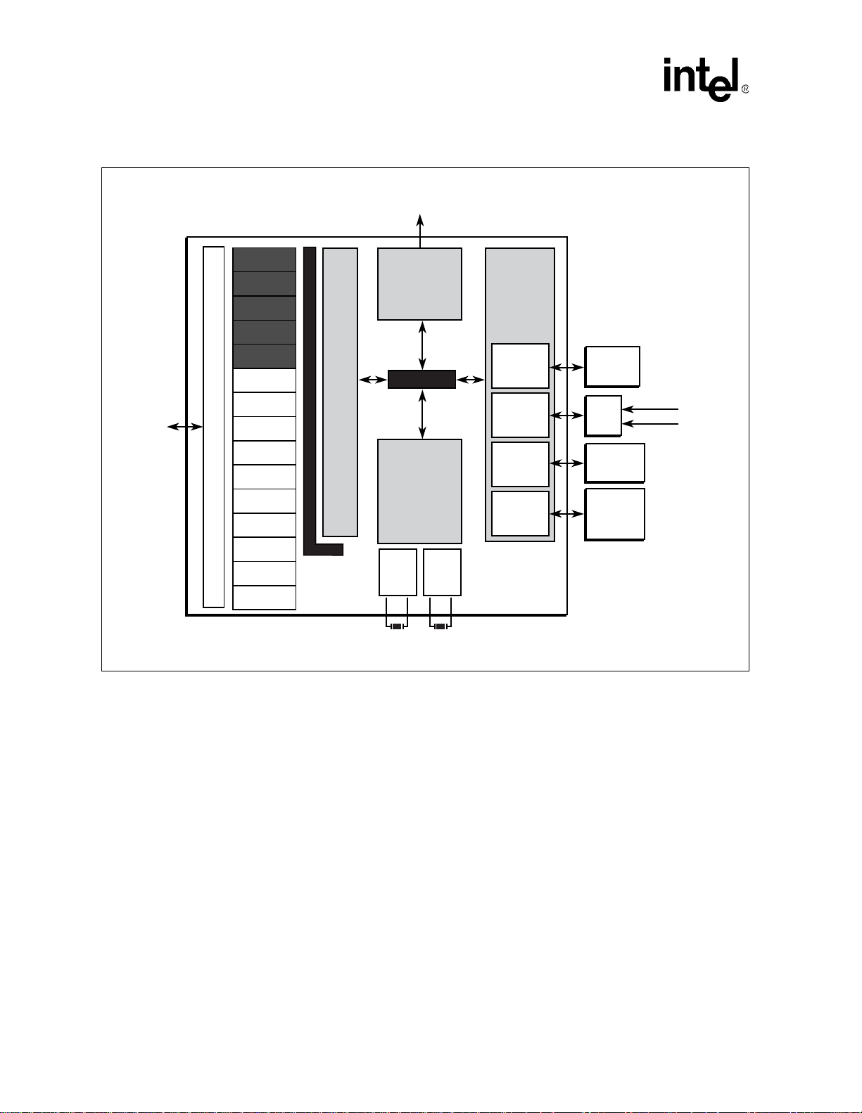
Figure 1-1 on page 1-2 is a block diagram of the applications processor.
PXA250 and PXA210 Applications Processors Design Guide 1-1
Page 10
Introduction
s
Figure 1-1. Applications Processor Block Diagram
RTC
OS Timer
PWM(2)
Int.
Controller
Clocks &
Power Man.
I2S
I2C
AC97
UART1
General Purpose I/O
UART2
Slow IrDA
Fast IrDA
SSP
USB
Client
MMC
and Bridge
Peripheral Bus
DMA Controller
Color or
Grayscale
LCD
Controller
System Bus
Megacell
Core
3.6864
MHz
Osc
32.768
KHz
Osc
Memory
Controller
Variable
Latency I/O
Control
PCMCIA
& CF
Control
Dynamic
Memory
Control
Static
Memory
Control
ASIC
XCVR
SDRAM/
SMROM
4 banks
ROM/
Flash/
SRAM
4 banks
Socket 0
Socket 1
A8651-01
The PXA250 applications processor package is: 256 pin, 17x17 mBGA – 32-b i t funct ionality . The
PXA210 applications processor package is: 225 pin, 13x13 MMAP – 16-bit functionality, a subset
of the PXA250 applications processor feature set.
Section 1.2.1, “Package Introduction” contains a breakdown of the features supported by the two
different packages.
1.2 Package Information
This section describes the package types, pinouts, and signal descriptions.
1.2.1 Package Introduction
Package features of the PXA250 applications processor are:
• Core frequencies supported - 100 MHz - 400 MHz
1-2 PXA250 and PXA210 Applications Processors Design Guide
Page 11

Introduction
• System memory interface
—100MHz SDRAM
— 4 MB to 256 MB of SDRAM memory
— Support for 16, 64, 12 8, or 256 Mbit DRAM techno l o gies
— 4 Banks of SDRAM, each supporting 64 MB of memory
— Clock enable (1 CKE pin is provided to put the entire SDRAM interface into self refresh)
— Supports as many as 6 static memory devices (SRAM, Flash, or VLIO)
• PCMCIA/Compact Flash card control pins
• LCD Controller pins
• Full Function UART
• Bluetooth UART
• MMC Controller pins
• SSP Pins
• USB Client Pins
• AC’97 Controller Pins
• Standard UART Pins
2
• I
C Controller pins
• PWM pins
• 15 dedicated GPIOs pins
• Integrated JTAG support
Package features of the PXA210 applications processor are:
• Core frequencies supported – 100 MHz, 133 MHz, 200 MHzSystem memory interface
— 100 MHz SDRAM, 16-bit only
— 2 MB to 128 MB of SDRAM memory
— Support for 16, 64, 12 8, or 256 Mbit DRAM techno l o gies
— 2 Banks of SDRAM, each supporting 64 MB of memory
— Supports as many as 6 static memory devices (SRAM, Flash, or VLIO)
• Clock enable (1 CKE pin is provided to put the entire SDRAM interface into self refresh)
• LCD Controller pins
• Bluetooth UART
• MMC Controller pins
• SSP Pins
• USB Client Pins
• AC97 Con t roller Pins
• Standard UART Pins
PXA250 and PXA210 Applications Processors Design Guide 1-3
Page 12
Introduction
2
• I
C Controller pins
• PWM pins
• 2 dedicated GPIOs pins
• Integrated JTAG support
1.2.2 Signal Pin Descriptions
Table 1-3 defines the signal descriptions for the applications processor.
Table 1-3. Signal Pin Descriptions (Sheet 1 of 7)
Name Type Description
Memory Controller Pins
MA[25:0] OCZ Memory address bus. This bus signals the address requested for memory accesses.
MD[15:0] ICOCZ Memory data bus. D[15:0] are used for 16-bit and 32-bit data modes.
Memory data bus. D[31:16]: These signals are the upper memory data bus address
MD[31:16] ICOCZ
nOE OCZ
nWE OCZ Memory write enable. Connect this signal to the write enables of memory devices.
nSDCS[3:0] OCZ
DQM[3:0] OCZ
nSDRAS OCZ
nSDCAS OCZ
SDCKE[0] OC
SDCKE[1] OC
SDCLK[2:0] OCZ
bits.
See Note [1]
Memory output enable. Connect this signal to the output enables of memory devices
to control their data bus drivers.
SDRAM CS for banks 0 through 3. Connect these signals to the chip select (CS) pins
for SDRAM. nSDCS0 is a three-state signal, while nSDCS1-3 are not three-state.
SDRAM DQM for data bytes 0 through 3. Connect these signals to the data output
mask enables (DQM) for SDRAM.
SDRAM RAS. Connect this signal to the row address strobe (RAS) pins for all banks
of SDRAM.
SDRAM CAS. Connect this signal to the column address strobe (CAS) pins for all
banks of SDRAM.
SDRAM and/or Synchronous Static Memory/SDRAM-like synchronous Flash clock
enable clock enable.
ConnectSDCKE[0] to the CKE pins of SMROM and SDRAM-timing Synchronous
Flash.
The memory controller provides control regist er bits for deassertion of each SDCKE
pin.
SDRAM device clock enable.
Connect SDCKE[1] to the clock enable pins of SDRAM. It is de-asserted (held low)
during sleep. SDCKE[1] is always deasserted upon reset.
The memory controller provides control regist er bits for deassertion of each SDCKE
pin.
See Note [1]
Use these clocks to clock synchronous memory devices:
SDCLK0 - connected to either SMROM or synchronous Flash devices
SDCLK1 - connected to SDRAM banks 0/1
SDCLK2 - connected to SDRAM banks 2/3
See Note [1]
1-4 PXA250 and PXA210 Applications Processors Design Guide
Page 13
Introduction
Table 1-3. Signal Pin Descriptions (Sheet 2 of 7)
Name Type Description
nCS[5]/
GPIO[33]
nCS[4]/
GPIO[80]
nCS[3]/
GPIO[79]
nCS[2]/
GPIO[78]
nCS[1]/
GPIO[15]
nCS[0] ICOCZ
RD/nWR OCZ Read/Write for static interface. Intended for use as a steering signal for buffering logic
RDY/
GPIO[18]
MBGNT/GP[13] ICOCZ
MBREQ/GP[14] ICOCZ
PCMCIA/CF Control Pins - PXA250 Applications Processor only
nPOE/ GPIO[48] ICOCZ
nPWE/
GPIO[49]
nPIOW/
GPIO[51]
nPIOR/
GPIO[50]
nPCE[2:1]/
GPIO[53, 52]
nIOIS16/
GPIO[57]
nPWAIT/
GPIO[56]
nPSKTSEL/
GPIO[54]
ICOCZ
ICOCZ
ICOCZ
ICOCZ
ICOCZ
ICOCZ
ICOCZ
ICOCZ
ICOCZ
ICOCZ
ICOCZ
ICOCZ
ICOCZ
Static chip selects. These signals are chip selects to static memory devices such as
ROM and Flash. They are individually programmable in the memory configuration
registers. nCS[5:3] may be used with variable data latency variable latency I/O
devices.
See Note [2]
Static chip select 0. This is the chip select for the boot memory. nCS[0] is a dedicated
pin.
Variable Latency I/O Ready pin (input)
See Note [2]
Memory Controller grant. (output) Notifies an external device that it has been granted
the system bus.
Memory Controller alternate bus master request. (input) Allows an external device to
request the system bus from the Memory Controller.
PCMCIA output enable. Output PCMCIA signal that performs reads from memory and
attribute space.
See Note [2]
PCMCIA write enable. Output signal that performs writes to memory and attribute
space.
See Note [2]
PCMCIA I/O write. Output signal that performs write transactions to the PCMCIA I/O
space.
See Note [2]
PCMCIA I/O read. Output signal that performs read transactions from the PCMCIA I/O
space.
See Note [2]
PCMCIA card enable. Output signals that selects a PCMCIA card. Bit one enables the
high byte lane and bit zero enables the low byte lane.
See Note [2]
I/O Select 16. Input signal from the PCMCIA card that indicates the current address is
a valid 16 bit wide I/O address.
See Note [2]
PCMCIA wait. Input signal that is driven low by the PCMCIA card to extend the length
of the transfers to/from the applications processor.
See Note [2]
PCMCIA socket select. Output signal used by external steering logic to route control,
address, and data signals to one of the two PCMCIA sockets. When PSKTSEL is low,
socket zero is selected. When PSKTSEL is high, socket one is selected. This signal
has the same timing as address.
See Note [2]
PXA250 and PXA210 Applications Processors Design Guide 1-5
Page 14
Introduction
Table 1-3. Signal Pin Descriptions (Sheet 3 of 7)
Name Type Description
nPREG/
GPIO[55]
LCD Controller Pins
L_DD(15:0)/
GPIO[73:58]
L_FCLK/
GPIO[74]
L_LCLK/
GPIO[75]
L_PCLK/
GPIO[76]
L_BIAS/
GPIO[77]
Full Function UART Pins
FFRXD/
GPIO[34]
FFTXD/
GPIO[39]
FFCTS/
GPIO[35]
FFDCD/
GPIO[36]
FFDSR/
GPIO[37]
FFRI/
GPIO[38]
FFDTR/
GPIO[40]
FFRTS/
GPIO[41]
Bluetooth UART Pins
BTRXD/
GPIO[42]
BTTXD/
GPIO[43]
BTCTS/
GPIO[44]
BTRTS/
GPIO[45]
MMC Controller Pins
MMCMD ICOCZ Multimedia Card Command pin (I/O)
ICOCZ
ICOCZ
ICOCZ
ICOCZ
ICOCZ
ICOCZ
ICOCZ
ICOCZ
ICOCZ
ICOCZ
ICOCZ
ICOCZ
ICOCZ
ICOCZ
ICOCZ
ICOCZ
ICOCZ
ICOCZ
PCMCIA register select. Output signal that indicates the target address is attribute
space, on a memory transaction. This signal has the same timing as address.
See Note [2]
LCD Controller display data
See Note [2]
LCD Frame clock
See Note [2]
LCD Line clock
See Note [2]
LCD pixel clock
See Note [2]
AC Bias Drive
See Note [2]
Full Function UART Receive pin
See Note [2]
Full Function UART Transmit pin
See Note [2]
Full Function UART Clear-to-Send pin
See Note [2]
Full Function UART Data-Carrier-Detect Pin
See Note [2]
Full Function UART Data-Set-Ready Pin:
See Note [2]
Full Function UART Ring Indicator Pin
See Note [2]
Full Function UART Data-Terminal-Ready pin
See Note [2]
Full Function UART Ready-to-Send pin
See Note [2]
Bluetooth UART Receive pin
See Note [2]
Bluetooth UART Transmit pin
See Note [2]
Bluetooth UART Clear-to-Send pin
See Note [2]
Bluetooth UART Data-Terminal-Ready pin
See Note [2]
1-6 PXA250 and PXA210 Applications Processors Design Guide
Page 15
Table 1-3. Signal Pin Descriptions (Sheet 4 of 7)
Name Type Description
MMDAT ICOCZ Multimedia Card Data Pin (I/O)
MMCCLK/GP[6] ICOCZ MMC clock. (output) Clock signal for the MMC Controller.
MMCCS0/GP[8] ICOCZ MMC chip select 0. (output) Chip select 0 for the MMC Controller.
MMCCS1/GP[9] ICOCZ MMC chip select 1. (output) Chip select 1 for the MMC Controller.
SSP Pins
SSPSCLK/
GPIO[23]
SSPSFRM/
GPIO[24]
SSPTXD/
GPIO[25]
SSPRXD/
GPIO[26]
SSPEXTCLK/
GPIO[27]
USB Client Pins
USB_P IAOA USB Client port positive Pin of differential pair.
USB_N IAOA USB Client port negative Pin of differential pair.
AC97 Controller Pins
BITCLK/
GPIO[28]
SDATA_IN0/
GPIO[29]
SDATA_IN1/
GPIO[32]
SDATA_OUT/
GPIO[30]
SYNC/
GPIO[31]
nACRESET OC
Standard UART and ICP Pins
IRRXD/
GPIO[46]
IRTXD/
GPIO[47]
I2C Controller Pins
SCL ICOCZ
ICOCZ
ICOCZ
ICOCZ
ICOCZ
ICOCZ
ICOCZ
ICOCZ
ICOCZ
ICOCZ
ICOCZ
ICOCZ
ICOCZ
Synchronous Serial Port Clock (output)
See Note [2]
Synchronous serial port Frame Signal (output)
See Note [2]
Synchronous serial port transmit (output)
See Note [2]
Synchronous serial port receive (input)
See Note [2]
Synchronous Serial port external clock (input)
See Note [2]
AC97 Audio Port bit clock (output)
See Note [2]
AC97 Audio Port data in (input)
See Note [2]
AC97 Audio Port data in (input)
See Note [2]
AC97 Audio Port data out (output)
See Note [2]
AC97 Audio Port sync signal (output)
See Note [2]
AC97 Audio Port reset signal (output)
This pin is a dedicated output.
IrDA Receive signal (input).
See Note [2]
IrDA Transmit signal (output).
Transmit pin for both the SIR and FIR functions.
See Note [2]
I2C clock (Bidirectional)
Bidirectional signal. When it is driving, it functions as an open collector device and
requires a pull up resistor. As an input, it expects standard CMOS levels.
Introduction
PXA250 and PXA210 Applications Processors Design Guide 1-7
Page 16
Introduction
Table 1-3. Signal Pin Descriptions (Sheet 5 of 7)
Name Type Description
I2C Data signal (bidirectional).
SDA ICOCZ
PWM Pins
PWM[1:0]/
GPIO[17,16]
Dedicated GPIO Pins
GPIO[1:0] ICOCZ
GPIO[14:2]) ICOCZ
GPIO[22:21] ICOCZ
Crystal Pins
PXTAL IA Input connection for 3.6864 Mhz crystal
PEXTAL OA Output connection for 3.6864 Mhz crystal
TXTAL IA Input connection for 32.768 khz crystal
TEXTAL OA Output connection for 32.768 khz crystal
48MHz/GP[7] ICOCZ 48 MHz clock. (output) Peripheral clock output derived from the PLL.
RTCCLK/GP[10] I COC Z Real time clock. (output) HZ output derived from the 32kHz or 3.6864MHz output.
3.6MHz/GP[11] ICOCZ 3.6864 MHz clock. (output) Output from 3.6864 MHz oscillator.
32kHz/GP[12] ICOCZ 32 kHz clock. (output) Output from the 32 kHz oscillator.
Miscellaneous Pins
BOOT_SEL
[2:0]
PWR_EN OCZ
nBATT_FAULT IC
ICOCZ
IC
Bidirectional signal. When it is driving, it functions as an open collector device and
requires a pull up resistor. As an input, it expects standard CMOS levels.
Pulse Width Modulation channels 0 and 1 (outputs)
See Note [2]
General Purpose I/O: These two pins are contained in both the PXA250
applications processors. They are preconfigured at a hard reset (nRESET) as wakeup
sources for both rising and falling edge detects.
These GPIOs do not have alternate functions and are intended to be used as the main
external sleep wakeup stimulus.
General Purpose I/O
See Note [1]
See Note [2]
General Purpose I/O
Additional general purpose I/O pins.
Boot programming select pins. These pins are sampled to indicate the type of boot
device present per the following table;
BOOT_SEL[2:0] Description
000Asynchronous 32-bit ROM
001Asynchronous 16-bit ROM
100One 32-bit SMROM
101One 16 bit SMROM
110Two 16 bit SMROMs (32 bit bus)
111Reserved
Power Enable. Active high Output.
PWR_EN enables the external power supply. Negating it signals the power supply
that the system is going into sleep mode and that the VDD power supply should be
removed.
Battery Fault. Active low input.
The assertion of nBATT_FAULT causes the applications processor
Mode.The applications processor
is asserted. Use nBATT_F AUL T signal to flag a critical power failure, such as the main
battery being removed. Minimum assertion time for nBATT_FAULT is 1ms.
will not recognize a wakeup event while this signal
and PXA210
to enter Sleep
1-8 PXA250 and PXA210 Applications Processors Design Guide
Page 17
Introduction
Table 1-3. Signal Pin Descriptions (Sheet 6 of 7)
Name Type Description
VDD Fault. Active low input.
nVDD_FAULT IC
nRESET IC
nRESET_OUT OC
JTAG Pins
nTRST IC
TDI IC JTAG test interface data input. Note this pin has an internal pullup resistor.
TDO OCZ
TMS IC JTAG test interface mode select. Note this pin has an internal pullup resistor.
TCK IC
TEST IC Test Mode. You should ground this pin. This pin is for manufacturing purposes only.
TESTCLK I C Test Clock. Use this pin for test purposes only. An end user should ground this pin.
Power and Ground Pins
VCC SUP
VSS SUP
PLL_VCC SUP P ositive supply for PLLs and oscillators must be shorted to VCC.
PLL_VSS SUP Gr ound supply for the PLL. Must be connected to common ground plane on the PCB.
VCCQ SUP
VSSQ SUP
VCCN SUP
nVDD_FAULT causes the applications processor
is ignored after a wakeup event until the power supply timer completes (approximately
10 ms). use the nVDD_FAUL T signal to flag a low battery . Minimum assertion time for
nVDD_FAULT is 1 ms.
Hard reset. Active low input.
nRESET is a level sensitive input which starts the processor from a known address. A
LOW level causes the current instruction to terminate abnormally, and all on-chip state
to be reset. When nRESET is driven HIGH, the processor re-starts from address 0.
nRESET must remain LOW until the power supply is stable and the internal 3.6864
MHz oscillator has come up to speed. While nRESET is LOW the processor performs
idle cycles.
Reset Out. Active low output.
This signal is asserted when nRESET is asserted and de-asserts after nRESET is
negated but before the first instruction fetch. nRESET_OUT is also asserted for “soft”
reset events (sleep, watchdog reset, GPIO reset)
JTAG Test Interface Reset. Resets the JTAG/Debug port. If JTAG/Debug is used,
drive nTRST from low to high either before or at the same time as nRESET. If JTAG is
not used, nTRST must be either tied to nRESET or tied low. Intel recommends that a
JTAG/Debug port be added to all systems for debug and download. See Chapter 9 for
details.
JTAG test interface data output. Note this pin does NOT have an internal pullup
resistor.
JTAG test interface reference Clock. TCK is the reference clock for all transfers on the
JTAG test interface.
NOTE: This pin needs an external pulldown resistor.
Positive supply for the internal logic. Connect this supply to the low voltage (.85 -
1.65v) supply on the PCB.
Ground supply for the internal logic. Connect these pins to the common ground plane
on the PCB.
Positive supply for all CMOS I/O except memory bus and PCMCIA pins. Connect
these pins to the common 3.3v supply on the PCB.
Ground supply for all CMOS I/O except memory bus and PCMCIA pins. Connect
these pins to the common ground plane on the PCB.
Positive supply for memory bus and PCMCIA pins. Connect these pins to the common
3.3 V or 2.5 V supply on the PCB.
to enter Sleep Mode. nVDD_FAULT
PXA250 and PXA210 Applications Processors Design Guide 1-9
Page 18
Introduction
Table 1-3. Signal Pin Descriptions (Sheet 7 of 7)
Name Type Description
VSSN SUP
BATT_VCC SUP
NOTES:
1. Not pinned out for the PXA210 applications processor.
2. GPIO Reset Operation: After any reset, these pins are configured as GPIO inputs by default. The input buffers for these pins
are disabled to prevent current drain and must be enabled prior to use by clearing the Read Disable Hold (RDH) bit.
To use a GPIO pin as an alternate function, follow this sequence:
1) Program the pin to the desired direction (input or output) using the GPIO Pin Direction Registers (GPDR).
2) Enable the input buffer by clearing the RDH bit, described above.
3) If needed, select the desired alternate function by programming the proper bits in the GPIO Alternate Function
Register (GAFR).
Ground supply for memory bus and PCMCIA pins. Connect these pins to the common
ground plane on the PCB.
Backup battery connection. Connect this pin to the backup battery supply. If a backup
battery is not required then this pin may be connected to the common 3.3v supply on
the PCB.
1-10 PXA250 and PXA210 Applications Processors Design Guide
Page 19
Figure 1-2. PXA250 Applications Processor
Introduction
PXA250 and PXA210 Applications Processors Design Guide 1-11
Page 20
Introduction
T a ble 1-4. PXA250 Applications Processor Pinout — Ballpad Number Order (Sheet 1 of 3)
Ball # Signal Ball # Signal Ball # Signal
A1 VCCN F7 GPIO[10] L13 GPIO[2]
A2 L_DD[13]/GPIO[71] F8 FFRTS/GPIO[41] L14 VSSQ
A3 L_DD[12]/GPIO[70] F9 SSPSCLK/GPIO[23] L15 TEXTAL
A4 L_DD[11]/GPIO[69] F10 FFDTR/GPIO[40] L16 TXTAL
A5 L_DD[9]/GPIO[67] F11 VCC M1 MA[14]
A6 L_DD[7]/GPIO[65] F12 GPIO[9] M2 MD[21]
A7 GPIO[11] F13 BOOT_SEL[2] M3 MA[15]
A8 L_BIAS/GPIO[77] F14 GPIO[8] M4 VCCN
A9 SSPRXD/GPIO[26] F15 VSSQ M5 MD[1]
A10 SDATA_OUT/GPIO[30] F16 VSSQ M6 MD[6]
A11 SDA G1 MA[0] M7 MD[7]
A12 FFDCD/GPIO[36] G2 VSSN M8 DQM[0]
A13 FFRXD/GPIO[34] G3 nSDCS[2] M9 MD[8]
A14 FFCTS/GPIO[35] G4 nWE M10 MD[15]
A15 BTCTS/GPIO[44] G5 nOE M11 BATT_VCC
A16 SDATA_IN1/GPIO[32] G6 nSDCS[1] M12 GPIO[22]
B1 DQM[1] G7 VCC M13 nPREG/GPIO[55]
B2 DQM[2] G8 VSSQ M14 VCCN
B3 L_DD[15]/GPIO[73] G9 VCC M15 VSSN
B4 GPIO[14] G10 VSSQ M16 nIOIS16/GPIO[57]
B5 GPIO[13] G11 TESTCLK N1 MD[22]
B6 GPIO[12] G12 TEST N2 VSSN
B7 L_DD[3]/GPIO[61] G13 BOOT_SEL[1] N3 MA[16]
B8 L_PCLK/GPIO[76] G14 VCCQ N4 MD[0]
B9 SSPEXTCLK/GPIO[27] G15 GPIO[7] N5 VCCN
B10 FFRI/GPIO[38] G16 BOOT_SEL[0] N6 MD[4]
B11 FFDSR/GPIO[37] H1 MA[2] N7 VCCN
B12 USB_N H2 MA[1] N8 nCS[0]
B13 BTRXD/GPIO[42] H3 MD[16] N9 VCCN
B14 BTRTS/GPIO[45] H4 VCCN N10 MD[13]
B15 IRRXD/GPIO[46] H5 MD[17] N11 VCCN
B16 MMDAT H6 MA[3] N12 DREQ[0]/GPIO[20]
C1 RDY/GPIO[18] H7 VSSQ N13 VCCN
C2 VSSN H8 VSS N14 DREQ[1]/GPIO[19]
C3 L_DD[14]/GPIO[72] H9 VSS N15 GPIO[21]
C4 VSSQ H10 VCC N16 nPWAIT/GPIO[56]
C5 L_DD[8]/GPIO[66] H11 nTRST P1 MA[17]
1-12 PXA250 and PXA210 Applications Processors Design Guide
Page 21
Introduction
Table 1-4. PXA250 Applications Processor Pinout — Ballpad Number Order (Sheet 2 of 3)
Ball # Signal Ball # Signal Ball # S ignal
C6 VCCQ H12 TCK P2 MA[19]
C7 L_DD[2]/GPIO[60] H13 TMS P 3 VCCN
C8 VSSQ H14 GPIO[6] P4 MA[25]
C9 BITCLK/GPIO[28] H15 TDI P5 MA[23]
C10 VCCQ H16 TDO P6 MD[24]
C11 VSSQ J1 MA[7] P7 MD[26]
C12 USB_P J2 VSSN P8 MD[27]
C13 VCCQ J3 MA[6] P9 nCS[2]/GPIO[78]
C14 V SSQ J4 MD[18] P10 MD[29]
C15 IRTXD/GPIO[47] J5 MA[5] P11 MD[12]
C16 V SS J6 MA[4] P12 MD[31]
D1 SDCLK[2] J7 VCC P13 nPO E/ GPIO[ 48]
D2 SDCLK[0] J8 VSS P 14 nPCE[1]/GPIO[52]
D3 RDnWR J9 VSS P15 VSSN
D4 VCCN J10 VSS Q P16 nPSKTSEL/GPIO[54]
D5 L_DD[10]/GPIO[68] J11 GPIO[5] R1 MA[18]
D6 L_DD[5]/GPIO[63] J12 GPIO[4] R2 VSSN
D7 L_DD[1]/GPIO[59] J13 nRESET R3 MA[20]
D8 L_LCLK/GPIO[75] J14 VSSQ R4 VSSN
D9 SSPTXD/GPIO[25] J15 PLL_VCC R5 MA[22]
D10 nA CRESET J16 PLL_VSS R6 VSSN
D11 SCL K1 MA[8] R7 MD[25]
D12 PWM[1]/GPIO[17] K2 MA[9] R8 VSSN
D13 B TTXD/GPIO[43] K3 MD[19] R9 MD[10]
D14 MMCMD K4 VCCN R10 VSSN
D15 VCCQ K5 MA[10] R11 MD[30]
D16 VSSQ K6 MA[11] R12 VSSN
E1 nSDRAS K7 VSSQ R13 nCS[4]/GPIO[80]
E2 VSSN K8 VCC R14 VSSN
E3 SDCKE[1] K9 VSSQ R15 nPIOW/GPIO[51]
E4 SDCKE[0] K10 VCC R16 nPCE[2]/GPIO[53]
E5 L_DD[6]/GPIO[64] K11 nRESET_OUT T1 VSS
E6 L_DD[4]/GPIO[62] K 12 nBATT_FAULT T2 VCCN
E7 L_DD[0]/GPIO[58] K13 nVDD_FAULT T3 MD[23]
E8 L_FCLK/GPIO[74] K 14 GPIO[3] T4 MA[21]
E9 SSPSFRM/GPIO[24] K15 PXTAL T5 MA[24]
E10 SDATA_IN0/GPIO[29] K16 PEXTAL T6 MD[3]
E11 SYNC/GPIO[31] L1 MA[12] T7 M D[5]
PXA250 and PXA210 Applications Processors Design Guide 1-13
Page 22
Introduction
T a ble 1-4. PXA250 Applications Processor Pinout — Ballpad Number Order (Sheet 3 of 3)
Ball # Signal Ball # Signal Ball # Signal
E12 PWM[0]/GPIO[16] L2 VSSN T8 nCS[1]/GPIO[15]
E13 FFTXD/GPIO[39] L3 MA[13] T9 nCS[3]/GPIO[79]
E14 VCCQ L4 MD[20] T10 MD[9]
E15 VSSQ L5 MD[2] T11 MD[11]
E16 VSSQ L6 VCC T12 MD[14]
F1 nSDCS[0] L7 DQM[3] T13 nCS[5]/GPIO[33]
F2 nSDCS[3] L8 MD[28] T14 nPWE/GPIO[49]
F3 nSDCAS L9 VCC T15 nPIOR/GPIO[50]
F4 VCCN L10 GPIO[0] T16 VCCN
F5 SDCLK[1] L11 PWR_EN
F6 VSSQ L12 GPIO[1]
1-14 PXA250 and PXA210 Applications Processors Design Guide
Page 23
Figure 1-3. PXA210 Applications Processor
φ
Introduction
PXA250 and PXA210 Applications Processors Design Guide 1-15
Page 24

Introduction
T a ble 1-5. PXA210 Applications Processor Pinout — Ballpad Number Order (Sheet 1 of 2)
Ball # Signal Ball # Signal Ball # Signal
A1 DQM[1] F1 VSSN L1 VSSN
A2 L_DD[14]/GPIO[72] F2 nSDCS[0] L2 VCCN
A3 L_DD[10]/GPIO[68] F3 nSDRAS L3 MA[12]
A4 VSSQ F4 nSDCS[1] L4 MA[13]
A5 L_DD[6]/GPIO[64] F5 VCC L5 MA[11]
A6 L_DD[2]/GPIO[60] F6 L_DD[8]/GPIO[66] L6 VSSQ
A7 L_LCLK/GPIO[75] F7 L_FCLK/GPIO[74] L7 MD[2]
A8 SPPSCLK/GPIO[23] F8 SSPRXD/GPIO[26] L8 MD[6]
A9 SPPEXTCLK/GPIO[27] F9 VCC L9 VSSN
A10 nACRESET F10 FFTXD/GPIO[39] L10 MD[11]
A11 PWM[1]/GPIO[17] F11 VCC L11 BATT_VCC
A12 VSSQ F12 VSSQ L12 GPIO[54]
A13 FFRXD/GPIO[34] F13 TESTCLK L13 GPIO[55]
A14 BTCTS/GPIO[44] F14 BOOT_SEL[0] L14 GPIO[57]
A15 IRRXD/GPIO[46] F15 TEST L15 GPIO[0]
B1 RDY/GPIO[18] G1 MA[0] M1 MA[14]
B2 VSSN G2 nOE M2 MA[15]
B3 L_DD[13]/GPIO[71] G3 nWE M3 VCCN
B4 L_DD[9]/GPIO[67] G4 VCCN M4 MA[16]
B5 VSSQ G5 VSSN M5 VCCN
B6 L_DD[3]/GPIO[61] G6 RDnW R M6 VSSN
B7 L_PCLK/GPIO[76] G7 VSS M7 MD[3]
B8 VSSQ G8 VSS M8 MD[7]
B9 BITCLK/GPIO[28] G9 VSS M9 nCS[1]/GPIO[15]
B10 SDA G10 BTRXD/GPIO[42] M10 MD[10]
B11 VSSQ G11 nTRST M11 MD[ 13]
B12 USB_N G12 TDI M12 GPIO[48]
B13 BTRTS/GPIO[45] G13 TCK M13 GPIO[52]
B14 IRTXD/GPIO[47] G14 TMS M14 VSSN
B15 MMDAT G15 TDO M15 GPIO[56]
C1 SDCKE[1] H1 VCCN N1 VSSN
C2 SDCKE[0] H2 VSSN N2 MA[18]
C3 VCCN H3 MA[2] N3 VSS1
C4 L_DD[12]/GPIO[70] H4 MA[1] N4 MA[22]
C5 VCCQ H5 VCC N5 MA[24]
C6 L_DD[4]/GPIO[62] H6 VSSQ N6 VCCN
C7 L_BIAS/GPIO[77] H7 VSS N7 VCC
1-16 PXA250 and PXA210 Applications Processors Design Guide
Page 25

Introduction
Table 1-5. PXA210 Applications Processor Pinout — Ballpad Number Order (Sheet 2 of 2)
Ball # Signal Ball # Signal Ball # S ignal
C8 VCCQ H8 VSS N8 VSSN
C9 SDATA_IN0/GPIO[29] H9 VSS N9 DQM[0]
C10 PWM[0]/GPIO[16] H10 VSSQ N10 VCCN
C11 USB_P H11 VCC N11 MD[12]
C12 BTTXD/GPIO[43] H12 VSSQ N12 VSSN
C13 VSSQ H13 VCC N13 nCS[5]/GPIO[33]
C14 V SS H14 PLL_VCC N14 GPIO[53]
C15 VCCQ H15 PLL_VSS N15 VCCN
D1 VCC J1 MA[5] P1 MA[17]
D2 VSSQ J2 MA[6] P2 VSSN
D3 SDCLK[1] J3 VSSN P3 VCCN
D4 L_DD[15]/GPIO[73] J4 MA[4] P4 MA[23]
D5 VCC J5 MA[3] P5 MD[0]
D6 L_DD[5]/GPIO[63] J6 VSSQ P6 VSSN
D7 L_DD[0]/GPIO[58] J7 VSS1 P7 MD[4]
D8 SPPSFRM/GPIO[24] J8 VSS1 P8 VCCN
D9 SDATA_OUT/GPIO[30] J9 VSS1 P9 nCS[2]/GPIO[78]
D10 SCL J10 VSSQ P10 MD[8]
D11 SDATA_IN1/GPIO[32] J11 nRESET P11 VCCn
D12 B OOT_SEL[1] J12 nRESET_OUT P12 MD[15]
D13 VSSQ J13 P W R_EN P13 VCCN
D14 VSSQ J14 nVDD_FAULT P14 GPIO[50]
D15 VSSQ J15 nBATT_FAULT P15 VSSQ
E1 nSDCAS K1 MA[8] R1 MA[19]
E2 VCCN K2 MA[9] R2 MA[20]
E3 VSSN K3 MA[10] R3 MA[21]
E4 SDCLK[0] K4 MA[7] R4 MA[25]
E5 L_DD[11]/GPIO[69] K5 VCCN R5 MD[1]
E6 L_DD[7]/GPIO[65] K6 VCC R6 VCCN
E7 L_DD[1]/GPIO[59] K7 VSSQ R7 MD[5]
E8 SSPTXD/GPIO[25] K8 VCC R8 nCS[0]
E9 SYNC/GPIO[31] K9 VSSQ R9 nCS[3]/GPIO[79]
E10 VCCQ K10 VCC R10 MD[9]
E11 MMCMD K11 GPIO[1] R11 VSSN
E12 VCCQ K12 TEX TAL R12 MD[14]
E13 VSSQ K13 TXTAL R13 nCS[4]/GPIO[80]
E14 VSSQ K14 PEXTAL R14 nPWE/GPIO[49]
E15 BOOT_SEL[2] K15 PXTAL R15 GPIO[51]
PXA250 and PXA210 Applications Processors Design Guide 1-17
Page 26

Introduction
1-18 PXA250 and PXA210 Applications Processors Design Guide
Page 27

System Memory Interface 2
This section is the design guidelines for the system memory interface.
2.1 Overview
The external memory bus interface for the applications processor supports:
• 100 MHz SDRAM at 3.3 V
• 100 MHz SDRAM at 2.5 V
• Synchronous and asynchronous Burst mode and Page mode Flash
• Synchronous Mask ROM (SMROM)
• Page Mode ROM
• SRAM
• SRAM-like Variable Latency I/O (VLIO)
• PCMCIA expansion memory
• Compact Flash
Use the memory interface configuration registers to program the memory types. Refer to
Figure 1-1, “Applicati ons Processor Block Diagra m” on page 1-2 fo r the block diagram of the
Memory Controller configuration. Refer to Figure 2-1, “Memory Address Map” on page 2-3 for
the applications processor memory map. Refer to Table 2-3, “Normal Mode Memory Address
Mapping” on page 2-6 for alternate mode address mapping.
PXA250 and PXA210 Applications Processors Design Guide 2-1
Page 28
System Memory Interface
Figure 2-1. General Memory Interface Configuration
PXA250
Memory
Controller
Interface
nSDCS<0>
nSDCS<1>
SDCLK<1>, SDCKE<1>
nSDCS<2>
nSDCS<3>
SDCLK<2>, SDCKE<1>
DQM<3:0>
nSDRAS, nSDCAS
MD<31:0>
MA<25:0>
Card Control
nCS<0>
nCS<1>
nCS<2>
SDCLK<0>,
nCS<3>
SDCKE<0>
SDRAM Partition 0
SDRAM Partition 1
SDRAM Partition 2
SDRAM Partition 3
Static Bank 0
Static Bank 1
Static Bank 2
Static Bank 3
SDRAM Memory Interface
Up to 4 partitions of SDRAM
memory (16- or 32-bit wide)
Buffers and
Transceivers
Static Memory or
Variable Latency I/O Interface
Up to 6 banks of ROM, Flash,
SRAM, Variable Latency I/O,
(16- or 32-bit wide)
NOTE:
Static Bank 0 must be populated by
“bootable” memory
Card Memory Interface
Up to 2-socket support.
Requires some
external buffering.
nCS<4>
nCS<5>
RDY
Static Bank 4
Static Bank 5
Synchronous Static Memory Interface
Up to 4 banks of synchronous
static memory (nCS<3:0>).
(16- or 32-bit wide)
NOTE:
Static Bank 0 must be populated by
“bootable” memory
2-2 PXA250 and PXA210 Applications Processors Design Guide
Page 29
T a ble 2-1. Memory Address Map
0x6000 0000 Reserved Address Space
0x5C00 0000 Reserved Addres s Space
0x5800 0000 Reserved Address Space
0x5400 0000 Reserved Address Space
0x5000 0000 Reserved Address Space
0x4C00 0000 Reserved Addres s Space
0x4800 0000 Memory Mapped Registers (Memory Ctl)
0x4400 0000 Memory Mapped Registers (LCD)
0x4000 0000 Memory Mapped Registers (Peripherals)
0x3000 0000 PCMCIA/CF – Slot 1
0x2000 0000 PCMCIA/CF – Slot 0
0x1C00 0000 Reserved Addres s Space
0x1800 0000 Reserved Address Space
0x1400 0000 Static Chip Select 5
0x1000 0000 Static Chip Select 4
0x0C00 0000 Static Chip Select 3
0x0800 0000 Static Chip Select 2
0x0400 0000 Static Chip Select 1
0x0000 0000 Static Chip Select 0
System Memory Interface
2.2 SDRAM Interface
The applications processor supports an SDRAM interface at a maximum frequency of 100 MHz.
The SDRAM Interface supports four 16-bit or 32-bit wide partitions of SDRAM. Each partition is
allocated 64 MBytes of the internal memory map. However, the actual size of each partition is
dependent on the parti cular SDRAM c onfiguration used. The four partitions are divided into two
partition pairs: the 0/1 pair and the 2/3 pair. Both partitions within a pair (for example, partition 0
and partition 1) must be identical in size and configuration; however, th e two pairs can be different.
For example, the 0/1 pair can be 100 MHz SDRAM on a 32-bit data bus, while the 2/3 pair can be
50 MHz SDRAM on a 16-bit data bus.
Note: For proper SDRAM operation above 50 MHz, 22 ohm series resistors must be placed on the
memory address lines.
2.3 SDRAM memory wiring diagram
Figure 2-2, “SDRAM Memory System Example” on page 2-4 is a wiring diagram example that
shows a system using 1Mword x 16-bit x 4-bank SDRAM devices for a total of 48 Mbytes. Refer
to Section 2.5, “SDRAM Address Mapping” on page 2-6 to determine the individual SDRAM
component address.
PXA250 and PXA210 Applications Processors Design Guide 2-3
Page 30
System Memory Interface
Figure 2-2. SDRAM Memory System Example
nSDCS(3:0)
nSDRAS, nSDCAS, nWE, CKE(1)
SDCLK(2:1)
MA(23:10)
MD(31:0)
DQM(3:0)
15:0
31:16
2
3
0
1
0
1
0
1
4Mx16
SDRAM
nCS
nRAS
nCAS
nWE
CKE
CLK
addr(11:0)
BA(1:0)
DQML
DQMH
DQ(15:0)
4Mx16
SDRAM
nCS
nRAS
nCAS
nWE
CKE
CLK
addr(11:0)
BA(1:0)
DQML
DQMH
DQ(15:0)
1
1
1
1
4Mx16
SDRAM
nCS
nRAS
nCAS
nWE
CKE
CLK
addr(11:0)
BA(1:0)
DQML
DQMH
DQ(15:0)
4Mx16
SDRAM
nCS
nRAS
nCAS
nWE
CKE
CLK
addr(11:0)
BA(1:0)
DQML
DQMH
DQ(15:0)
21:10
23:22
2
2
2
2
4Mx16
SDRAM
nCS
nRAS
nCAS
nWE
CKE
CLK
addr(11:0)
BA(1:0)
DQML
DQMH
DQ(15:0)
4Mx16
SDRAM
nCS
nRAS
nCAS
nWE
CKE
CLK
addr(11:0)
BA(1:0)
DQML
DQMH
DQ(15:0)
2-4 PXA250 and PXA210 Applications Processors Design Guide
Page 31

2.4 SDRAM Support
Table 2-2 shows the SDRAM memory types and densities that are supported by the applications
.
Table 2-2. SDRAM Memory Types Supported by the Applications Processor
processor.
System Memory Interface
Partition Siz e
(Mbyte/Partition)
16-bit
Bus
2 Mbyte 4 Mbyte 1M x 16 16 Mbit 1 2 1 x 11 x 8 8 Mbyte 16 Mbyte 4 8
4 Mbyte 8 Mbyte 2 M x 8 16 Mb it 2 4 1 x 11 x 9 16 Mbyte 32 Mbyte 8 16
8 Mbyte 16 Mbyte 4 M x 4 16 Mbit 4 8 1 x 11 x 10 32 Mbyte 64 Mbyte 16 32
N/A 8 Mbyte 2 M x 32 64 Mbit N/A 1 2 x 11 x 8 N/A 32 Mbyte N/A 4
8 Mbyte 16 Mbyte 4 M x 16 64 Mbit 1 2
16 Mbyte 32 Mbyte 8 M x 8 64 Mbit 2 4
32 Mbyte 64 Mbyte 16 M x 4 64 Mbit 4 8
16 Mbyte 32 Mbyte 8 M x 16 128 Mbit 1 2 2 x 12 x 9 64 Mbyte
32 Mbyte 64 Mbyte 16 M x 8 128 Mbit 2 4 2 x 12 x 10
64 Mbyte N/A 32 M x 4 128 Mbit 4 8 2 x 12 x 11
32-bit
Bus
SDRAM
Configu-
ration
(Words x
Bits)
Chip
Size
Number Chips/
Partition
16-bit
Bus
32-bit
bus
Bank Bits x
Row bits x
Column
Bits
1 x 13 x 8
2 x 12 x 8
1 x 13 x 9
2 x 12 x 9
1 x 13 x 10
2 x 12 x 10
Maximum
Memory
(4 Partitions)
16-bit
Bus
32 Mbyte 64 Mbyte 4 8
64 Mbyte
128
Mbyte
128
Mbyte
256
Mbyte
32-bit
Bus
128
Mbyte
256
Mbyte
128
Mbyte
256
Mbyte
N/A 16 32
Total Number
of Chips
16-bit
Bus
32-bit
816
16 32
48
816
Bus
32 Mbyte 64 Mbyte
64 Mbyte N/A 32 M x 8 256 Mbit 2 4 2 x 13 x 10
16 M x
16
256 Mbit 1 2 2 x 13 x 9
128
Mbyte
256
Mbyte
256
Mbyte
N/A 8 16
48
PXA250 and PXA210 Applications Processors Design Guide 2-5
Page 32

System Memory Interface
2.5 SDRAM Address Mapping
SDRAM Address Mapping is shown in Table 2-3 and Table 2-4.
Table 2-3. Normal Mode Memory Address Mapping
SDRAM
Device Technology
1Mx16 16Mbit 1x11x8 BS0 A10 A9 A8 A7 A6 A5 A4 A3 A2 A1 A0
2Mx8 16Mbit 1x11x9 BS0 A10 A9 A8 A7 A6 A5 A4 A3 A2 A1 A0
4Mx4 16Mbit 1x11x10 BS0 A10 A9 A8 A7 A6 A5 A4 A3 A2 A1 A0
2Mx32 64Mbit 2x11x8 BS1BS0A10A9A8A7A6A5A4A3A2A1A0
4Mx16/4Mx32 64Mbit/128Mbit 2x12x8 BS1 BS0 A11 A10 A9 A8 A7 A6 A5 A4 A3 A2 A1 A0
8Mx8/8Mx16 64Mbit/128Mbit 2x12x9 BS1 BS0 A11 A10 A9 A8 A7 A6 A5 A4 A3 A2 A1 A0
16Mx4/16Mx8 64Mbit/128Mbit 2x12x10 BS1 BS0 A11 A10 A9 A8 A7 A6 A5 A4 A3 A2 A1 A0
32Mx4 128Mbit 2x12x11 BS1 BS0 A11 A10 A9 A8 A7 A6 A5 A4 A3 A2 A1 A0
8Mx32 256Mbit 2x13x8 BS1BS0A12A11A10A9A8A7A6A5A4A3A2A1A0
16Mx16 256Mbit 2x13x9 BS1BS1A12A11A10A9A8A7A6A5A4A3A2A1A0
# Bits
Bank x
Row x
1x12x8 BS0A11A10A9A8A7A6A5A4A3A2A1A0
1x12x9 BS0A11A10A9A8A7A6A5A4A3A2A1A0
1x12x10 BS0A11A10A9A8A7A6A5A4A3A2A1A0
1x12x11 BS0A11A10A9A8A7A6A5A4A3A2A1A0
1x13x8 BS0 A12 A11 A10 A9 A8 A7 A6 A5 A4 A3 A2 A1 A0
1x13x9 BS0 A12 A11 A10 A9 A8 A7 A6 A5 A4 A3 A2 A1 A0
1x13x10 BS0 A12 A11 A10 A9 A8 A7 A6 A5 A4 A3 A2 A1 A0
1x13x11 BS0 A12 A11 A10 A9 A8 A7 A6 A5 A4 A3 A2 A1 A0
2x11x9 BS1BS0A10A9A8A7A6A5A4A3A2A1A0
2x11x10 BS1BS0A10A9A8A7A6A5A4A3A2A1A0
A24 A23 A22 A21 A20 A19 A18 A17 A16 A15 A14 A13 A12 A11 A10
Col
The applications processor pin mapping to SDRAM devices
(The address lines at the top of the columns are the processor address lines)
2-6 PXA250 and PXA210 Applications Processors Design Guide
Page 33

System Memory Interface
Table 2-4. Applications Processor Compatibility Mode Address Line Mapping
SDRAM
Device Technology
1Mx16 16Mbit 1x11x8 BS0 A10 A9 A8 A7 A6 A5 A4 A3 A2 A1 A0
2Mx8 16Mbit 1x11x9 BS0 A10 A9 A8 A7 A6 A5 A4 A3 A2 A1 A0
4Mx4 16Mbit 1x11x10 BS0 A10 A9 A8 A7 A6 A5 A4 A3 A2 A1 A0
2Mx32 64Mbit 2x11x8 BS1BS0A10A9A8A7A6A5A4A3A2A1A0
4Mx16/4Mx32 64Mbit/128Mbit 2x12x8 BS1 BS0 A11 A10 A9 A8 A7 A6 A5 A4 A3 A2 A1 A0
8Mx8/8Mx16 64Mbit/128Mbit 2x12x9 BS1 BS0 A11 A10 A9 A8 A7 A6 A5 A4 A3 A2 A1 A0
16Mx4/16Mx8 64Mbit/128Mbit 2x12x10 BS1 BS0 A11 A10 A9 A8 A7 A6 A5 A4 A3 A2 A1 A0
32Mx4 128Mbit 2x12x11 BS1 BS0 A11 A10 A9 A8 A7 A6 A5 A4 A3 A2 A1 A0
8Mx32 256Mbit 2x13x8 A12BS1BS0A11A10A9A8A7A6A5A4A3A2A1A0
16Mx16 256Mbit 2x13x9 A12BS1BS0A11A10A9A8A7A6A5A4A3A2A1A0
# Bits
Bank x
Row x
Col
1x12x8 A11BS0A10A9A8A7A6A5A4A3A2A1A0
1x12x9 A11BS0A10A9A8A7A6A5A4A3A2A1A0
1x12x10 A11BS0A10A9A8A7A6A5A4A3A2A1A0
1x12x11 A11BS0A10A9A8A7A6A5A4A3A2A1A0
1x13x8 A12 A11 BS0 A10 A9 A8 A7 A6 A5 A4 A3 A2 A1 A0
1x13x9 A12 A11 BS0 A10 A9 A8 A7 A6 A5 A4 A3 A2 A1 A0
1x13x10 A12 A11 BS0 A10 A9 A8 A7 A6 A5 A4 A3 A2 A1 A0
1x13x11 A12 A11 BS0 A10 A9 A8 A7 A6 A5 A4 A3 A2 A1 A0
2x11x9 BS1BS0A10A9A8A7A6A5A4A3A2A1A0
2x11x10 BS1BS0A10A9A8A7A6A5A4A3A2A1A0
A24 A23 A22 A21 A20 A19 A18 A1 7 A16 A15 A14 A13 A12 A11 A10
The applications processor pin mapping to SDRAM devices
(The address lines at the top of the columns are the processor address lines)
2.6 Static Memory
2.6.1 Overview
The applications processor external memory bus interface supports the following static memory
types:
• Synchronous and asynchronous Burst mode and Page mode Flash
• Synchronous Mask ROM (SMROM)
• Page Mode ROM
• SRAM
• SRAM-like Variable Latency I/O (VLIO)
• PCMCIA expansion memory
• Compact Flash
PXA250 and PXA210 Applications Processors Design Guide 2-7
Page 34

System Memory Interface
Memory types are programmable through the memory interface configuration registers.
Six chip selects control the static memory interface, nCS<5:0>. All are configurable for nonburst
ROM or Flash memory, burst ROM or Flash, SRAM, or SRAM-like variable latency I/O devices.
The variable latency I/O interface differs from SRAM in that it allows the data ready input signal
(RDY) to insert a variable number of memory-cycle-wait states. The data bus width for each chip
select region may be programmed to be 16-bi t or 32-bit. nCS<3:0> are also configurable for
Synchronous Static Memory.
For SRAM and variable latency I/O implementations, DQM<3:0> signals are used for the write
byte enables, where DQM<3> corresponds to the MSB. The applications processor supplies 26bits of byte address for access of up to 64 Mbytes per chip select. However, when the address is
sent out on the MA pins, MA reflects the actual address, not the byte address. The lower one or two
internal address bits are truncated appropriately.
2.6.2 Boot Time Defaults
Booting configuration is device specific. For example, you cannot use a 32-bit memory booting
configuration with a PXA210 applications processor . Table 2-5 shows valid booting configurations
based on processor type, while Table 2-6 shows boot selection definitions. See Section 7.10.2,
“Boot-Time Configurations” in the Intel® PXA250 and PXA210 Applications Processors
Developer’s Manual for more detailed descriptions of these Boot Time Configurations.
Table 2-5. Valid Booting Configurations Based on Package Type
Processor Type Valid Booting Configurations
0 (PXA210
applications
processor)
1 (PXA250
applications
processor)
001
101
111
000
001
100
101
110
111
Table 2-6. BOOT_SEL Definitions (Sheet 1 of 2)
BOOT_SEL
210
0 0 0 Asynchronous 32-bit ROM
0 0 1 Asynchronous 16-bit ROM
100
1 32-bit Synchronous Mask ROM (64 Mbits)
2 16-bit Synchronous Mask ROMs = 32-bits (32 Mbits each)
Boot From . . .
2-8 PXA250 and PXA210 Applications Processors Design Guide
Page 35

T a ble 2-6. BOOT_SEL Definitions (Sheet 2 of 2)
System Memory Interface
BOOT_SEL
210
1 0 1 1 16-bit Synchronous Mask ROM (64 Mbits)
1 1 0 2 16-bit Synchronous Mask ROMs = 32-bits (64 Mbits each)
1 1 1 1 16-bit Synchronous Mask ROM (64 Mbits)
Boot From . . .
2.6.3 SRAM / ROM / Flash / Sync hronous Fast Flash Memory Options
Table 2-7 contains the AC specification for SRAM / ROM / Flash / Synchronous Fast Flash.
Table 2-7. SRAM / ROM / Flash / Synchronous Fast Flash AC Specifications
Symbol Description
SRAM / ROM / Flash / Synchronous Fast Flash (WRITES) (Asynchronous)
tromAS
tromAH
tromASW MA(25:0) setup to nWE asserted 30 25.5 22.5 20.4 18 ns, 3
tromAHW MA(25:0) hold after nWE de-asserted 10 8.5 7.5 6.8 6 ns, 1
tromCES nCS setup to nWE asserted 20 17 15 13.6 12 ns, 2
tromCEH nCS hold after nWE de-asserted 10 8.5 7.5 6.8 6 ns, 1
tromDS
tromDSWH
tromDH
tromNWE
NOTES:
1. This number represents 1 MEMCLK period
2. This number represents 2 MEMCLK periods
MA(25:0) setup to nOE, nSDCAS (as
nADV) asserted
MA(25:0) hold after nCS, nOE,
nSDCAS (as nADV) de-asserted
MD(31:0), DQM(3:0) write data setup to
nWE asserted
MD(31:0), DQM(3:0) write data setup to
nWE de-asserted
MD(31:0), DQM(3:0) write data hold
after nWE de-asserted
nWE high time between beats of write
data
99.5 118.0 132.7 147.5 165.9
10 8.5 7.5 6.8 6 ns, 1
10 8.5 7.5 6.8 6 ns, 1
10 8.5 7.5 6.8 6 ns, 1
20 17 15 13.6 12 ns, 2
10 8.5 7.5 6.8 6 ns, 1
20 17 15 13.6 12 ns, 2
MEMCKLK
Units
Notes
2.6.4 Variable Latency I/O Interface Overview
Both reads and writes for VLIO differ from SRAM in that the PXA250 applications processor
samples the data-ready input, RDY. The RDY signal is level sensitive and goes through a two-stage
synchronizer on input. When the internal RDY signal is high, the I/O device is ready for data
transfer. This means that for a transaction to complete at the minimum assertion time for either
nOE or nPWE (RDF+1), th e RDY signal must be high two clocks prior to the mini mum assertion
time for either nOE or nPWE (RDF-1). Data will be latched on the rising edge of memclk once the
internal RDY signal is high and the minimum assertion time of RDF+1 has been reached. Once the
PXA250 and PXA210 Applications Processors Design Guide 2-9
Page 36

System Memory Interface
data has been latched, the address may change on the next rising edge of MEMCLK or any cycles
thereafter. The nOE or nPWE signal de-asserts one MEMCLK after data is latched. Before a
subsequent data beat, nOE or nPWE remains deasserted for RDN+1 memory cycles. The chip
select and byte selects, DQM[3:0], remain asserted for one memory cycle after the burst’s final
nOE or nPWE deassertion. Refer to
Figure 2-3 for 32-Bit Variable Latency I/O read timing and
Figure 2-8 for Variable Latency I/O Interface AC Specifications
Figure 2-3. 32-Bit Variable Latency I/O Read Timing (Burst-of-Four, One Wait Cycle Per Beat)
0ns 100ns 200ns 300ns
memlk
nCS[0]
tAS
MA[25:2]
MA[1:0]
tASRW0
nOE
nPWE
RDnWR
RDY
MD[31:0]
DQM[3:0]
nCS[1]
012 3
"00"
tAH
tCES RDN+1
tASWN
tCEH
RDF+1+Waits
"0000"
RRR+1
A8867-01
T able 2-8. Variable Latency I/O Interface AC Specifications (Sheet 1 of 2)
Symbol Description
Variable Latency IO Interface (VLIO) (Asynchronous)
tvlioAS MA(25:0) setup to nCS asserted 10 8.5 7.5 6.8 6 ns, 1
tvlioASRW
tvlioAH
tvlioCES nCS setup to nOE or nPWE asserted 20 17 15 13.6 12 ns, 2
tvlioCEH
MA(25:0) setup to nOE or nPWE
asserted
MA(25:0) hold after nOE or nPWE deasserted
nCS hold after nOE or nPWE deasserted
99.5 118.0 132.7 147.5 165.9
10 8.5 7.5 6.8 6 ns, 1
10 8.5 7.5 6.8 6 ns, 1
10 8.5 7.5 6.8 6 ns, 1
MEMCKLK
Units
Notes
2-10 PXA250 and PXA210 Applications Processors Design Guide
Page 37

System Memory Interface
T able 2-8. Variable Latency I/O Interface AC Specifications (Sheet 2 of 2)
Symbol Description
tvlioDSW
tvlioDSWH
tvlioDHW
tvlioDHR
tvlioRDYH
tvlioNPWE
NOTES:
1. This number represents 1 MEMCLK period
2. This number represents 2 MEMCLK periods
MD(31:0), DQM(3:0) write data setup to
nPWE asserted
MD(31:0), DQM(3:0) write data setup to
nPWE de-asserted
MD(31:0), DQM(3:0) hold after nPWE
de-asserted
MD(31:0) read data hold after nOE deasserted
RDY hold after nOE, nPWE deasserted
nPWE, nOE high time between beats of
write or read data
99.5 118.0 132.7 147.5 165.9
10 8.5 7.5 6.8 6 ns, 1
20 17 15 13.6 12 ns, 2
10 8.5 7.5 6.8 6 ns, 1
00000ns
00000ns
20 17 15 13.6 12 ns, 2
MEMCKLK
2.6.5 External Logic for PCMCIA Implementation
The PXA250 applications processor requires external glue logic to complete the PCMCIA socket
interface. Figure 2-4, “Expansion Card External Logic for a Two-Socket Configuration” on page 2-
12 and Figure 2-5, “Expansion Card External Logic for a One-So cket Confi gurati on ” on page2-13
show general solutions for one and two socket configurations. Use GPIO or memory-mapped
external registers to control the PCMCIA interface’s reset, power selection (V
drive enables. These diagrams show the logical connections necessary to support hot insertion
capability. For dual-voltage support, level shifting buffers are required for all the applications
processor input signals. Hot insertion capability requires each socket be electrically isolated from
the other and from the remainder of the memory system. If one or both of these features are not
required, you may eliminate some of the logic shown in these diagrams. T he applications processor
allows either 1-socket or 2-socket solutions. In the 1-socket solution, only minimal glue logic is
required (typically for the data transceiver s, add ress buf fer s, and level shifting buffer s.) To achieve
this some of the signals are routed through dual-duty GPIO pins. The nOE of the transceivers is
driven through the PSKTSEL pin, which is not needed in the one-socket solution. The DIR pin of
the transceiver is driven through the RDnWR pin. A GPIO is used for the three-state signal of the
address and nPWE lines. These signals are used for memories other than the card interface and
must be three-stated.
and VPP), and
CC
Units
Notes
Note: For 2.5 V VCCN, 5 V to 2.5 V level shifters are required.
Note: PCMCIA is only implemented on the PXA250 applications processor.
In the 2-socket solution, all pins assume their normal duties and glue logic is necessary for proper
operation of the system. The pull-ups shown are included fo r comp lian ce with PC Card Standard -
Volume 2 - Electrical Specification. Remove power from these pull-ups during sleep to avoid
unnecessary power consumption. Refer to Table 2-9 for the PCMCIA or compact Flash card
interface AC specifications.
PXA250 and PXA210 Applications Processors Design Guide 2-11
Page 38

System Memory Interface
Figure 2-4. Expansion Card External Logic for a Two-Socket Configuration
PXA250
Applications
Processor
Socket 0
D(15:0)
GPIO(w)
GPIO(x)
GPIO(y)
GPIO(z)
PSKTSEL
MA(25:0)
nPREG
nPCE(1:2)
nPOE,
nPWE
nPIOW,
nPIOR
nPWAIT
DIR
OE#
nPCEx
nPOE
nPIOR
nPCEx
6 6
DIR OE#
D(15:0)
Socket 1
D(15:0)
CD1#
CD2#
CD1#
CD2#
RDY/BSY#
RDY/BSY#
A(25:0)
REG#
A(25:0)
CE(1:2)#
OE#
WE#
IOR#
6
IOW#
WAIT#
WAIT#
REG#
CE(1:2)#
OE#
WE#
IOR#
IOW#
WAIT#
WAIT#
IOIS1616#
nPIOIS16
IOIS1616#
A8863-02
2-12 PXA250 and PXA210 Applications Processors Design Guide
Page 39

System Memory Interface
Figure 2-5. Expansion Card External Logic for a One-Socket Configuration
PXA250
Socket 0
MD<15:0> D<15:0>
nOE
DIR
RD/nWR
GPIO<w>
GPIO<x>
nPCD0
nPCD1
nCD<1>
nCD<2>
PSKTSEL
GPIO<y>
GPIO<z>
MA<25:0>
nPWE
nPREG
nPCE<2:1>
nPOE
nPIOR
nPIOW
PRDY_BSY0
PADDR_EN0
RDY/nBSY
A<25:0>
nWE
nREG
nCE<2:1>
nOE
nIOR
nIOW
5V to 3.3V
nPWAIT
nWAIT
5V to 3.3V
nIOIS16
nIOIS16
Table 2-9. Card Interface (PCMCIA or Compact Flash) AC Specifications (Sheet 1 of 2)
Symbol Description
Card Interface (PCMCIA or Compact Flash) (Asynchronous)
tcardAS
tcardAH
tcardDS
MA(25:0), nPREG, PSKTSEL, nPCE
setup to nPWE, nPOE, nPIOW, or
nPIOR asserted
MA(25:0), nPREG, PSKTSEL, nPCE
hold after nPWE, nPOE, nPIOW, or
nPIOR de-asserted
MD(31:0) setup to nPWE, nPOE,
nPIOW, or NPIOR asserted
99.5 118.0 132.7 147.5 165.9
20 17 15 13.6 12 ns, 1
10 8.5 7.5 6.8 6 ns, 1
10 8.5 7.5 6.8 6 ns, 1
MEMCKLK
PXA250 and PXA210 Applications Processors Design Guide 2-13
Units
Notes
Page 40

System Memory Interface
Table 2-9. Card Interface (PCMCIA or Compact Flash) AC Specifications (Sheet 2 of 2)
Symbol Description
tcardDH
tcardCMD
NOTE:
1. These numbers are minmums. They can be much larger based on the programmable Card Interface
timing registers.
MD(31:0) hold after nPWE, nPOE,
nPIOW, or NPIOR de-asserted
nPWE, nPOE, nPIOW, or nPIOR
command assertion
99.5 118.0 132.7 147.5 165.9
10 8.5 7.5 6.8 6 ns, 1
30 25.5 22.5 20.4 18 ns, 1
2.6.6 DMA / Companion Chip Interface
Connect a companion chip to the applications processor via:
• Alternate Bus Master Mode
• Variable Latency I/O
• Flow through DMA
These connections are illustrated in Figure 2-6 and Figure 2-7.
MEMCKLK
Units
Notes
2-14 PXA250 and PXA210 Applications Processors Design Guide
Page 41

Figure 2-6. Alternate Bus Master Mode
PXA250
System Memory Interface
EXTERNAL SYSTEM
SDCKE<1>
SDCLK<1>
PXA250
Memory
Controller
MBREQ
MBGNT
PXA250
GPIO
Block
nSDCS(0)
nSDRAS
nSDCAS
nWE
MA<25:0>
DQM<3:0>
MD<31:0>
GPIO<13> (MBGNT)
GPIO<14> (MBREQ)
External
SDRAM
Bank 0
Companion
Chip
PXA250 and PXA210 Applications Processors Design Guide 2-15
Page 42

System Memory Interface
Figure 2-7. Variable Latency I/O
PXA250
PXA250
Memory
Controller
EXTERNAL SYSTEM
nCS(0,1,2,3,4,5)
nOE
nPWE
MA<25:0>
DQM<3:0>
MD<31:0>
RDY
Companion
Chip
2-16 PXA250 and PXA210 Applications Processors Design Guide
Page 43

System Memory Interface
2.7 System Memory Layout Guidelines
2.7.1 System Memory Topologies (Min and Max Si mulated
Loading)
Figure 2-8, Figure 2-9, Figure 2-10, and Figure 2-11 are the topologies that where simulated to
develop the trace length recommendations in Section 2.7.2. These topologies are for reference
only.
Figure 2-8. CS, CKE, DQM, CLK, MA minimum loading topology
CS, CKE, DQM,
CLK, MA
Figure 2-9. CS, CKE, DQM, CLK, MA Maximum Loading Topology
CS, CKE, DQM,
CLK, MA
SDRAM
SDRAM
SDRAM
SDRAM
SDRAM
Figure 2-10. MD Minimum Loading Topology
MD
PXA250 and PXA210 Applications Processors Design Guide 2-17
SDRAM
Page 44

System Memory Interface
Figure 2-11. MD maximum loading to pology
MD
SDRAM SDRAM
AUXAUXAUXAUX
2.7.2 System Memory Recommended Trace Lengths
Table 2-10 details the minimum and maximum trace lengths that were simulated for the
applications processor. These trace lengths are not the absolute trace lengths that will work given
the loading conditions. The trace lengths in Table 2-10 are measured from the applications
processor to the individual component pins. The board impedance for the simulations was 60ohm
+/- 10%.
Table 2-10. Minimum and Maximum Trace Lengths for the SDRAM Signals
Signal
CS, CKE, DQM 0.75 in 4.5 in
CLK 1.0 in 4.25 in
MA 1.0 in 4.5 in
MD 1.0 in 4.25 in
Min
Trace Length
Max
Trace Length
2-18 PXA250 and PXA210 Applications Processors Design Guide
Page 45

LCD Display Controller 3
This chapter describes sample hardware connections from the PXA250 applications processor to
various types of LCD controllers. Active (TFT) as well as passive (DSTN) displays are discussed
as well as single and dual panel displays. These should not be considered the only possible ways to
connect an LCD panel to the PXA250 applications processor, but should serve as a reference to
assist with hardware design considerations. Other panels, for example panels without L_FCLK or
L_LCLK, have been successfully connected to the PXA250.
3.1 LCD Display Overview
The PXA250 applications processor supports both active and passive LCD displays. Active
displays generally produce better looking images, but at a higher cost. Passive displays are
generally less expensive, but their displays are inferior to active displays. However, recent
advances in dithering technology are closing the quality gap between passive and active displays.
Note: Names used for “LCD Panel Pin” are representative names and may no t match those on all LCD
panels. Refer to the LCD panel reference documentation for the actual name.
3.2 Passive (DSTN) Displays
Several different types of passive displays are available in both color and monochrome. These
maybe single or dual panel displays. Additionally, some monochrome displays use double-pixel
data mode (twice the number of pixels as a normal mo nochrome display). W ith the exception of the
number of data pins required, all of these choices affect the sof tware configu ration and support, not
the system hardware design. In fact, most pa ssive displays use a single interconn ection scheme. For
information on the software changes and performance considerations of the various display
options, refer to the PXA250 and PXA210 Applications Processors Developer’s Manual.
Passive displays drive dithered data to the LCD panel - which means that for each pixel clock cycle
a single data line drives an ON/OFF signal for one color of a single pixel.
Table 3-1 describes the number of L_DD pins required for the various types of passive displays, as
well as which LCD data pins are used for which panel (upper or lowe r).
Table 3-1. LCD Controller Data Pin Utilization (Sheet 1 of 2)
Color/
Monochrome
Panel
Monochrome Single No Whole L_DD<3:0>
Monochrome Single Yes Whole L_DD<7:0>
Monochrome Dual No
Color Single N/A Whole L_DD<7:0>
Single/
Dual Panel
Double-Pixel
Mode
Screen Portion Pins
1
Top L_DD<3:0>
Bottom L_DD<7:4>
PXA250 and PXA210 Applications Processor Design Guide 3-1
Page 46

LCD Display Controller
Table 3-1. LCD Controller Data Pin Utilization (Sheet 2 of 2)
Color/
Monochrome
Panel
Color Dual N/A
NOTE: 1. Double pixel data mode (DPD)=1.
Single/
Dual Panel
Double-Pixel
Mode
Screen Portion Pins
Top L_DD<7:0>
Bottom L_DD<15:8>
For passive displays , the pins describ ed in Table 3-2 are required connections between the PXA250
applications processor and your LCD panel.
T able 3-2. Passive Display Pins Required
PXA250 Pin LCD Panel Pin PIn Type
L_DD DU_x, DL_x Output
L_PCLK Pixel_Clock Output
L_LCLK Line_Clock Output
L_FCLK Frame_Clock Output
L_BIAS Bias Output
N/A Vcon
NOTES:
1. “Pin Type” is in reference to the PXA250 applications processor. Therefore, outputs are pins that drive a signal from the processor to another
device.
2. Vcon is a signal external to the PXA250 applications processor. Please re fer to “Contrast Voltage” on page 8
2
N/A
1
Definition
Data lines used to transmit either four or eight data values at a time to
the LCD display. For monochrome displays, each pin value represents
a single pixel; for passive color, groupings of three pin values represent
one pixel (red, green, and blue data values). Either the bottom four pins
(L_DD<3:0>), the bottom 8 pins (L_DD<7:0>) or all 16 pixel data pins
(L_DD<15:0>)will be used as shown in Table3-1
Pixel Clock - used by the LCD display to clock the pixel data into the
line shift register.
Line Clock - used by the LCD display to signal the end of a line of pixels
that transfers the line data from the shift register to the screen and
increment the line pointers.
Frame Clock - used by the LCD displays to signal the start of a new
frame of pixels that resets the line pointers to the top of the screen.
AC bias used to signal the LCD display to switch the polarity of the
power supplies to the row and column axis of the screen to counteract
DC offset.
Contrast Voltage - Adjustable voltage input to LCD panel - external
voltage circuitry is required (no pin available on PXA250).
3.2.1 Typical Connections for Passive Panel Displays
The following diagrams are typical connections and serve a guide for designing systems which
contain passive LCD displays. Panels differ on which is the panel’s lest significant bit (Refer to the
LCD panel reference documentation for the lest significant bit.) Each figure indicates the top-left
pixel (1,1) bit. While dual panels indicates the top-left pixel (1,n/2) of the upper and lower panel s
and color passive panels show the top-left-pixel color bits.
3.2.1.1 Passive Monochrome Single Panel Displays
Figure 3-1 is a typical single-panel-monochrome passive display connection.
3-2 PXA250 and PXA210 Applications Processor Design Guide
Page 47

LCD Display Controller
Figure 3-1. Single Panel Monochrome Passive Display Typical Connection
L_DD0 - Top left
L_DD1
L_DD2
L_DD3
PXA250 Processor
L_PCLK
L_LCLK
L_FCLK
L_BIAS
D0
D1
D2
D3
LCD Display
Pixel_Clock
Line_Clock
Frame_Clock
Bias
3.2.1.2 Passive Monochrome Single Panel Displays, Double-Pixel Data
Figure 3-2 shows typical connections for a single-panel-monochrome passive display using
double-pixel data mode.
Figure 3-2. Passive Monochrome Single Panel Displays, Double-Pixel Data Typical
Connection
D0
D1
D2
D3
D4
D5
LCD Display
D6
D7
PXA250 Processor
L_DD0 - Top left
L_DD1
L_DD2
L_DD3
L_DD4
L_DD5
L_DD6
L_DD7
L_PCLK
L_LCLK
L_FCLK
L_BIAS
Pixel_Clock
Line_Clock
Frame_Clock
Bias
3.2.1.3 Passive Monochrome Dual Panel Displays
Figure 3-3 is a typical dual-panel-monochrome passive display connection.
PXA250 and PXA210 Applications Processor Design Guide 3-3
Page 48

LCD Display Controller
Figure 3-3. Passive Monochrome Dual Panel Displays Typical Connection
L_DD0 - Top left for upper panel
L_DD1
L_DD2
L_DD3
PXA250 Processor
L_PCLK
L_LCLK
L_FCLK
L_BIAS
L_DD4 - Top left for lower panel
L_DD5
L_DD6
L_DD7
3.2.1.4 Passive Color Single Panel Displays
Figure 3-4 is a typical single-panel-color passive display connection.
Figure 3-4. Passive Color Single Panel Displays Typical Connection
L_DD0
L_DD1
L_DD2
L_DD3
L_DD4
PXA250 Processor
L_DD5 - Top left Blue
L_DD6 - Top left Green
L_DD7 - Top left Red
DU_0
DU_1
DU_2
DU_3
Pixel_Clock
Line_Clock
Frame_Clock
Bias
DL_0
DL_1
DL_2
DL_3
D0
D1
D2
D3
D4
D5
D6
D7
Upper Panel
LCD Display
Lower Panel
LCD Display
L_PCLK
L_LCLK
L_FCLK
L_BIAS
Pixel_Clock
Line_Clock
Frame_Clock
Bias
3.2.1.5 Passive Color Dual Panel Displays
Figure 3-5 is a typical dual-panel-color passive display connection.
3-4 PXA250 and PXA210 Applications Processor Design Guide
Page 49

Figure 3-5. Passive Color Dual Panel Displays Typical Connection
LCD Display Controller
L_DD0
L_DD1
L_DD2
L_DD3
L_DD4
L_DD5 - Top left Blue for upper panel
L_DD6 - Top left Green for upper panel
L_DD7 - Top left Red for upper panel
PXA250 Processor
L_PCLK
L_LCLK
L_FCLK
L_BIAS
L_DD8
L_DD9
L_DD10
L_DD11
L_DD12
L_DD13 - Top left Blue for lower panel
L_DD14 - Top left Green for lower panel
L_DD15 - Top left Red for lower panel
3.3 Active (TFT) Displays
Because data is sent to the panel as raw 16-bit pixel data, active displays require16 data pins in
order to transfer the pixel data from the controller. All 16 data lines are also required to drive one
pixel value. The 16 bits of da ta describe the intensity lev el of the red, green and blue for each pixel.
T ypically, this is formatted as 5 bits for red, 6 bits for green and 5 bits for blue, but this can vary by
display and is controlled by the software writing to the frame buffer. Refer to the display datasheet
to ensure that the correct the PXA250 applications processor LCD data lines are connected to the
correct LCD panel data lines.
DU_0
DU_1
DU_2
DU_3
DU_4
DU_5
DU_6
DU_7
Pixel_Clock
Line_Clock
Frame_Clock
Bias
DL_0
DL_1
DL_2
DL_3
DL_4
DL_5
DL_6
DL_7
Upper Panel
LCD Display
Lower Panel
Many active displays actually have more than 16 data lines - usually 1 8 (6 of each color). For these
panels it is recommended that the most significant lines of the panel lines are connected to the data
lines from the PXA250 applications processor. This maintains the panel’s full range of colors but
increases the granularity of the color spectrum with an insufficient number of data lines. All unused
panel data lines can be tied either high or low. Other options include tying the LSB of red and blue
to the next bit, R1 or B1.
For active displays, connect the pins described in Table 3-3 between the PXA250 applications
processor and the LCD panel.
PXA250 and PXA210 Applications Processor Design Guide 3-5
Page 50

LCD Display Controller
Table 3-3. Active Display Pins Required
PXA250 Pin LCD Panel Pin PIn Type
L_DD<15:0>
L_PCLK Clock Output
L_LCLK Horizontal Sync Output
L_FCLK Vertical Sync Output
L_BIAS
N/A Vcon
NOTES:
1. In reference to
applications processor to another device.
2. Vcon is a signal external to
R<4:0>,G<5:0>,
B<4:0>
DE (Data
Enable)
2
Output Data lines used to transmit the 16 bit data values to the LCD display.
Output
N/A
the PXA250 applications processor. Therefore, outputs are pins that drive a signal from the PXA250
the PXA250 applications processor. Please refer to Section 3.5.1, “Contrast Voltage” on page 8.
1
Pixel Clock - used by the LCD display to clock the pixel data into the
line shift register. In active mode this clock transitions constantly.
Line Clock - used by the LCD display to signal the end of a line of pixels
that transfers the line data from the shift register to the screen and
increment the line pointers. Also signals the panel to start a new line.
Frame Clock - used by the LCD displays to signal the start of a new
frame of pixels that resets the line pointers to the top of the screen.
AC biases used in active mode as a data enable signal when data
should be latched by the pixel clock from the data lines.
Contrast Voltage - Adjustable voltage input to LCD panel - external
voltage circuitry is required (no pin available on the PXA250
applications processor).
Definition
3.3.1 Typical connections for Active Panel Displays
Figure 3-6, “Active Color Display Typical Connection” on page 7 shows a typical connection for
an active panel display and should serve as a guide for designing systems which contain active
LCD displays. The MSB of each color is indicated. The panel is 18-bit, with the LSB of red and
blue tied to ground.
3-6 PXA250 and PXA210 Applications Processor Design Guide
Page 51

LCD Display Controller
Note: This example shows 6 red, 6 green and 6 blue bits on the LCD panel. However, different active
display panels might have more or different dat a lines. Consult the LCD p anel manufa cturer’s
datasheet for the actual data lines.
Figure 3-6. Active Color Display Typical Connection
PXA250 Processor
3.4 PXA250 Pinout
Table 3-4 describes the ball positio ns for the LCD controller on the PXA250 applications
processor.
L_DD0
L_DD1
L_DD2
L_DD3
L_DD4 - MSB of Blue
L_DD5
L_DD6
L_DD7
L_DD8
L_DD9
L_DD10 - MSB of Green
L_DD11
L_DD12
L_DD13
L_DD14
L_DD15 - MSB of Red
L_PCLK
L_LCLK
L_FCLK
L_BIAS
Clock
Horizontal Sync
Vertical Sync
Data Enable
G3
R1
B0
B1
B2
B3
B4
B5
G0
G1
G2
G4
G5
R0
R2
R3
R4
R5
LCD Panel
Table 3-4. PXA250 LCD Controller Ball Positions (Sheet 1 of 2)
Pin Name Ball Position
L_DD0 E7
L_DD1 D7
L_DD2 C7
L_DD3 B7
L_DD4 E6
L_DD5 D6
L_DD6 E5
L_DD7 A6
L_DD8 C5
L_DD9 A5
L_DD10 D5
L_DD11 A4
PXA250 and PXA210 Applications Processor Design Guide 3-7
Page 52

LCD Display Controller
Table 3-4. PXA250 LCD Controller Ball Positions (Sheet 2 of 2)
Pin Name Ball Posi tion
L_DD12 A3
L_DD13 A2
L_DD14 C3
L_DD15 B3
L_FCLK E8
L_LCLK D8
L_PCLK B8
Bias A8
3.5 Additional Design Considerations
3.5.1 Contrast Voltage
Many displays, both active and pa ssive, includ e a pin for adj usting the display contra st voltage.
This is a variable analog voltage that is supplied to the panel via an voltage source on the system
board. The contrast voltage is adjusted via a variable resistor on the circuit board.
The required voltage range and current capabilities vary between panel manufacturers. Consult the
datasheet for your panel to determine the variable voltage circuit design. Ensure that the contrast
voltage is stable, otherwise visual artifacts might result. Possible contrast-voltage circuits are often
suggested by the panel manufacture rs.
3.5.2 Backlight Inverter
One potential source of noise for the LCD panel can be the backlight inverter. Since this is a high
voltage device with frequent voltage inversions, it has the potential to inject spurious noise onto the
LCD panel lines. To minimize noise:
• Use a shielded backlight inverter
• Physically locate the inverter as far away from the LCD data lines and system board as
possible, usually located with the LCD panel
If power consumption is an issue, chose a backlig ht inverter that can be disab led thr oug h s oftware.
This lets you save power by automatically disabling the backlight if no activity occurs within a
preset period of time
3.5.3 Signal Routing and Buffering
Signal transmission rates between the LCD controller and the LCD panel are moderate, which
helps to simplify the design of the LCD system. The minimum Pix e l Clock Divider (PCD) value
results in a pixel clock rate of one half of the LCLK (this is not the L_LCLK of the LCD
controller.) The maximum LCLK for the PXA250 applications processor is 166 MHz, resulting in
a maximum pixel clock rate of 83 MHz. Thus, use of 100 MHz design considerations are suf ficient
to ensure LCD panel signal integrity.
3-8 PXA250 and PXA210 Applications Processor Design Guide
Page 53

LCD Display Controller
However, typical transfer rates are considerably less than 83 Mhz. For example, an 800x600 color
active display running at 75 Hz requires a transfer rate of approximately 36 MHz. To determined
this, calculate the number of pixels (800 x 600 = 480,000) and multiply by the screen refresh rate
(75 Hz). Since active panels replace 1 pixel of data with every clock cycle this determines the fin al
transfer rate. Active displays normally do not require refresh rates as high as 75 Hz, so you may use
a lower refresh rate to reduce transmission rates even more.
Passive displays often do require refresh r ates greater th an 75 Hz, which transfers more pixels each
clock cycle. For instance, a color passive display with 8 data lines transfers 2 2/3 pixels’ worth of
data each clock cycle. This divides the transmission rate by 2 2/3. Further reductions in the transfer
rate come by using dual panel displays which use twice as many data lines to transfer data - halving
the rate again.
Generally, this gives you lower transfer rates to even large displays and thus simpler design
considerations and fewer layout constraints.
When laying out your design, minimize trace length of the LCD panel signals and allow sufficient
spacing between signals to avoid crosstalk. Crosstalk decreases the signal integrity, especially the
data line signals.
LCD system design is not considered to be critical as infrequent or single bit errors are, typically,
not noticed by the user. Also, the errors are transitory, as the old data is constantly being replaced
with new data. Slower panel refresh rates increase the likelihood that a single error is noticed by the
user. However, there is an counteracting effect in that slower refresh rates relax LCD timing and
therefore result in fewer screen transmission errors. There are other factors related to choosing a
refresh rate for an LCD system, most significant is the impact on system bandwidth.
If you must use excessively long or poorly routed signals, one possible solution is to add buffers
between the PXA250 applications processor and the LCD panel. This helps strengthen the LCD
panel signal levels and synchronizes signal timing. However, this is usually not required as the
LCD panel timings are fairly relaxed. Since the LCD display essentially operates asynch ron ously
from the processor, the propagation delay of the buffers is not a major concern.
When mounting the LCD panel, it is critical to shield the touchscreen control lines, if present.
Noise from the LCD panel and its control signals can become injected in to the touchs creen con trol
lines, causing spurious touch interrupts or loss of resolution.
3.5.4 Panel Connector
Most LCD panels are connected to the system board via a connector, instead of being directly
mounted on the system board. This increases flexibility and ease of manufacture. Typically the
manufacturer of the panel recommends a particular connector for the panel. Follow the panel
manufacturer’s recommendation.
PXA250 and PXA210 Applications Processor Design Guide 3-9
Page 54

LCD Display Controller
3-10 PXA250 and PXA210 Applications Processor Design Guide
Page 55

USB Interface 4
4.1 Self Powered Device
Figure 4-1 shows the USB interface connection for a self-powered device. The 0 ohm resistors are
optional, and if not used, then connect USB UDC+ directly to the device UDC+ and connect USB
UDC- directly to device UDC-. The device UDC+ and UDC- pins match the impedance of a USB
cable, 90 ohms, without the use of external series resi stors. You may install 0 ohm resistors on your
board to compensate for minor differences between the USB cable and your board trace
impedance.
The 5 to 3.3 voltage divider is required since the device GPIO pins cannot exceed 3.3 V. This
voltage divider can be implemented in a number of ways. The most robust and expensive solution
is to use a MAX6348 Power-On-Reset device. This solution p roduces a v ery clean sig nal edge and
minimizes signal bounce. The more inexpensive solution is to use a 3.3 V line buffer with 5 V
tolerant inputs. This solution does not reduce signal bounce, so software must compensate by
reading the GPIO signal after it stabilizes. A third solution is to implement a signal bounce
minimization circuit that is 5 V tolerant, but produces a 3.3 V signal to the GPIO pin.
Note: If GPIOn and GPIOx are the same pin, never put the device to sleep while the USB cable is
connected to the device. During sleep, the USB controller is in reset and will not respond to the
host; after sleep, the device will not respond to its host-assigned address.
Figure 4-1. Self Powered Device
USB 5V
USB UDC+
USB UDC-
USB GND
5V to 3.3V
470K
1.5K
0 ohm
(optional)
0 ohm
(optional)
GPIOn
GPIOx
UDC+
UDC-
Board GND
4.1.1 Operation if GPIOn and GPIOx are Different Pins
Any GPIO pins can be defined as GPIOn and GPIOx. GPIOn should be a GPIO which can bring
the device out of sleep. Out of reset, configure GPIOx as an input that causes the UDC+ line to
float. GPIOn is configured as an input that causes an interrupt whenever a rising or falling edge is
PXA250 and PXA210 Applications Processors Design Guide 4-1
Page 56

USB Interface
detected. When an interrupt occurs, software must read the GPIOn pin to determine if the cable is
connected or not. GPIOn is 1 if the cable is connected or 0 if the cable is disconnected. If a USB
connect is detected, then software enables the UDC peripheral and drives a 1 onto the GPIOx pin to
indicate to the host PC a fast USB device is connected. If a USB disconnect is detected, then
software must configure the GPIOx pin as an input, configure the GPIOn pin to detect a wakeup
event, and then put the part into sleep mode.
Also, at any time, you may use software to put the part into sleep mode. Before entering sleep
mode, configure the GPIOx pin as an input to cause the UDC+ line to float. This looks like a
disconnect to the host PC. The device can then be put into sleep mode. When the device becomes
active, software must drive a 1 onto the GPIOx pin to indicate to the host PC a fast USB dev ice has
been connected.
4.1.2 Operation if GPIOn and GPIOx are the Same Pin
Out of reset, GPIOn is configured as an input and configured to cause an interrupt whenever a
rising or falling edge is detected. When an interrupt occurs, software must read the GPIOn pin to
determine if the cable is connected or not. This pin is 1 if the cable is connected or 0 if the cable is
disconnected. If the USB cable is connected, then software must enable the UDC peripheral before
the host sends the first USB command. If the USB cable is not connected, then software must
configure the GPIOn pin to detect a wakeup event, and then put the part into sleep mode.
4.2 Bus Powered Device
The applications processor cannot support a bus powered device model. When the host sends a
suspend, the device is requi red to cons ume less than 500uA (Section 7.2.3 of the USB spec version
1.1). The applications processor cannot limit its current consumption to 500 uA unless it enters
sleep mode. If it enters sleep mode, all USB registers are reset and it does not respond to its hostassigned address.
4-2 PXA250 and PXA210 Applications Processors Design Guide
Page 57

MultiMediaCard (MMC) 5
The MultiMediaCard (MMC) is a low cost data storage and communication media. The MMC
supports the translation protocol from a standard MMC or Serial Peripheral Interface (SPI) bus to
an application bus.
The MMC controller in the applications processor is compliant with The Mult iMediaCard System
Specification, Version 2.1. The only exception is one and three byte data transfers are not
supported. The MMC controller is capable of communicating with a card in MMC or SPI mode.
Your application is responsible for specifying the MMC controll er communication mode.
5.1 Schematics
The MultiMediaCard (MMC) controller on the applications processor supports MMC and SDCard
devices. (The MMC controller does not support SDCard nibble mode.) This section presents
several options on how to connect each type of device to the controller.
5.1.1 Signal Description
MMC controller signal functions are described in Table 5-1.
Table 5-1. MMC Signal Description
Signal Name Input/Output Description
MMCLK Output Clock signal to MMC
MMCMD BiDirectional Command line
MMDAT BiDirectional Data line
MMCCS0 Output Chip Select 0
MMCCS1 Output Chip Select 1
The MMCLK, MMCCS0, and MMCCS1 signals are routed through alternate functions within the
applications processor general purpose input/output (GPIO) module. Each of these signals can be
programmed to a particular GPIO pin.
The signals defined in The MultiMediaCard System Specification for an MMC device are CLK,
CMD, and DAT which correspond to the MMCLK, MMCMD, and MMDAT in the applications
processor, respectively. The two chip selects in the controller are for the MMC SPI mode and
correspond to the reserved pin of two different devices, defined in the specification.
The signals defined in the Physical Layer Specification of the SD Memory Card Specifications for
an SDCard device are CLK, CMD, and DAT0-DAT3. The obvious difference is the number of
DAT signals. In addition, the socket for an SDCard contains mechanical switches for write protect
(WP) and card detect (CD). For an SDCard to be connected to the MMC controller, only one data
line, DAT0, is used. Otherwise the signal mapping remains the same as an MMC device. The WP
and CD switches on the socket are discussed in Section 5.1.2, “How to Wire” on page 5-2.
PXA250 and PXA210 Applications Processors Design Guide 5-1
Page 58

MultiMediaCard (MMC)
5.1.2 How to Wire
Notice in the example schematic (Figure 5-1, “Applications Processor MMC and SDCard Signal
Connections” on page 5-3) an SDCard socket is used. The signals on the socket are defined in
Table 5-2.
Table 5-2. SDCard Socket Signals
Signal Name Pin #
DAT3 1
CMD 2
VSS1 3
VDD 4
CLK 5
VSS2 6
DAT0 7
DAT1 8
DAT2 9
As stated previously, the PXA250 MMC controller can be connected to either an MMC device or
an SDCard device, but you are limited to which device installs in which socket. Refer to Table 5-3
for information on sockets and device supported by the MMC controller.
T able 5-3. MMC Controller Supported Sockets and Devices
Sockets Devices Supported
SDCard socket
MMC socket MMC device
SDCard device
MMC device
Figure 5-1 is a schematic that supports both MMC an d SDC ar d devices. In the schematic, the
signals SA_MMCLK, SA_MMCMD, and SA_DAT correspond to the applications processor
signals MMCLK, MMCMD, and MMDAT, respectively. These three signals are also directly
connected to the socket.
5-2 PXA250 and PXA210 Applications Processors Design Guide
Page 59

MultiMediaCard (MMC)
Figure 5-1. Applications Processor MMC and SDCard Signal Connections
DC3P3V
J10
10K
Bottom Mount
CHECK II
WP
10
R229
COMM
11
100K
DAT2
CD_DAT3
CMD
VSS1
VDD
CLK
VSS2
DAT0
DAT1
CD
12
DC3P3V
MMC_WP
0
1
2
3
4
5
6
7
8
MMC_C50
SA_MMCCLK
CARD Selection Resistors and Values
Resistors SDCard MMC
R226
R227
R225
R228
R147
SA_MMDAT
DC3P3V
R150
47.5K
DNI
DNI
0
100K
C91
R226
SA_MMCMD
0.1uF
R225
0K
DNI
IF
0K
SD
0
100K
DNI
DNI
DNI IF MMC
DC3P3V
R227
R228
100K
100K
MMC_PWR
DNI
IF
SD
nMMC_DETECT
DNI
IF
MMC
U27
DC5P5V
MMC_ON
MIC5207- 3.38M5
3.3V LDO REG 180ns
1
VIN
2
GND
3
EN
LE33
VOUT
BYP
5
4
4.7uF
MMC_PWR
12
C92
A8698-01
MMC_CS0, which corresponds to the applications processor MMCCS0 signal, is connected to the
socket at pin 1. This connection is the SPI mode chip select and is available on both MMC and
SDCard. This pin is also labeled DAT3. DAT3 is only used with an SDCard in SDCard mode and
not available on the applications processor MMC controller.
The signals DAT1 and DAT2 are not connected because these are specific to SDCard operation in
SDCard mode.
PXA250 and PXA210 Applications Processors Design Guide 5-3
Page 60

MultiMediaCard (MMC)
Three other signals shown on the connector are COMM and the mechanical switches write protect
(WP) and card detect (CD). WP and CD are both connected to COMM via a mechanical switch
inside the socket when a device is inserted.
Three other signals shown on the connector are COMM and the mechanical switches WP and CD.
When a device is inserted in the example schematic ( Figure 5-1), WP may be and CD is connected
to COMM via a mechanical switch inside the socket
SDCard devices have a write protect tab. Depending on the position of the tab, the WP signal may
or may not be connected to the COMM signal. Connect the WP signal to a CPLD or other device
capable of indicating to the driver software that the card is write protected. In this example,
COMM is tied to a VCC and WP has a pu ll-down res istor. This causes a rising edge when the tab is
in the write protect position and the WP signal remains low when the tab is in the read/write
position.
The CD signal, MMC_DETECT, indicates to the MMC controller when a card is installed. It is
used for both an SDCard socket and an MMC socket. Since the MMC socket does not have the
mechanical CD switch, other measures must be taken to produce a card detect. Thus, the SDCard
and MMC cases are discussed separately.
Note: While this schematic shows two ways to create a card detect, it is recommended that an SDCard
socket be used if a card detect and write protection signal are desired even if only MMC devices
are being used.
5.1.2.1 SDCard Socket
When using Figure 5-1, “Applications Processor MMC and SDCard Signal Connections” on
page 5-3 as a template for your SDCard circuit design, all resistors labeled “DNI IF SD” should not
be installed and all resistors labeled “DNI IF MMC” should be installed in the circuit. Removing
R226 and inserting R225 causes the VSS2 signal on pin 6 to be tied to ground. Also, the SDC ard
needs a pull-down resistor in position R228.
SDCard sockets have a card detect switch internal to the socket. The CD signal is physically
connected to the COMM signal. Connect the CD signal to a CPLD or other device capable of
indicating to the driver software that a card has been inserted in the socket. In this example,
COMM is tied to a V
card is inserted while the CD signal remains low if no card is in the socket.
5.1.2.2 MMC Socket
When using Figure 5-1, “Applications Processor MMC and SDCard Signal Connections” on
page 5-3 as a template for your MMC circuit design, all resistors labeled “DNI IF MMC” should
not be installed and all resistors labeled “DNI IF SD” should be installed in the circuit. This causes
the VSS2 signal on pin 6 to be pulled-up through resistor R227.
Unlike SDCard sockets, MMC sockets do not have a card detect or write protect switch. In order to
implement this, a pull-up is placed on the VSS2 signal (pin 6 of the socket.) Since VSS2 and VSS1
are connected internally on the MMC device, the signal called nMMC_DETECT on the schematic
is driven low when the MMC device is inserted.
and CD has a pull-down resistor. This causes a rising edge on CD when a
CC
5-4 PXA250 and PXA210 Applications Processors Design Guide
Page 61

MultiMediaCard (MMC)
Warning: Connecting VSS 2 to something other than the power supply ground violates The MultiMediaCard
System Specification, Ve rsion 2.1. Because the MMC specification does not state that VSS1 and
VSS2 must be connected internal to the MMC device, the design in Figure 5-1 may not work with
all MMC devices. Use caution when using the card detection method shown in Figure 5-1.
5.1.3 Simplified S ch e ma t ic
Figure 5-2 shows another SDCard socket. In this case, all applications processor signals are
connected to the socket. This socket does not have a common signal for the write protect and card
detect and are connected to the two tabs shown on the left side of the diagram. Inserting a card into
the socket may cause the write protect signal and will cause the card detect signal to change states
and must be interpreted by the CPLD software.
Figure 5-2. Applications Processor MMC to SDCard Simplified Signal Connection
+3.3V
Jx
ESD
WP
CD
DAT1
DAT0
VSS2
CLK
VDD
VSS1
CMD
CD/DAT3
DAT2
GND
5638 SDMC_NORMAL_SPRG_EJCT
12 13
Kyoc 10 5638 009 353 833
Rx
10K Ω
11
10
8
7
6
5
4
3
2
1
9
5% 0.1W
Rx
10K Ω
5% 0.1W
Rx
10K Ω
5% 0.1W
Rx
10K Ω
5% 0.1W
SD_WP
SD_CD
MMDAT
MMCLK
MMCMD
MMCCS0
A8699-01
PXA250 and PXA210 Applications Processors Design Guide 5-5
Page 62

MultiMediaCard (MMC)
5.1.4 Pull-up and Pull-down
Table 5-4 and Table 5-5 show the pull-up and pull-down resistors required for SDCard and MMC
devices according to their respective specifications.
Table 5-4. SDCard Pull-up and Pull-down Resistors
Signal P ul l-up or Pull-down Min Max Remark
CMD pull-up 10kΩ 100kΩ Prevents bus floating
DAT0-DAT3 pull-up 10kΩ 100kΩ Prevents bus floating
1
WP
NOTE: 1. This resistor is shown in the specification but the value is not specified
Table 5-5. MMC Pull-up and Pull-down Resistors
Signal Pull-up or Pull-down Min Max Remark
CMD pull-up 4.7kΩ 100kΩ Prevents bus floating
DAT pull-up 50kΩ 100kΩ Prevents bus floating
pull-up — — Any value sufficient to prevent bus floating
5.2 Utilized Features
The applications processor MultiMediaCard controller has these features:
• Data transfer rates as fast as 20 Mbps
• A16 bit response FIFO
• Dual receive data FIFOs
• Dual transmit FIFOs
• Support for two MMCs in either MMC or SPI mode
The sample schematics in this section support MMC and SDCard and are configured to use MMC
or SPI mode.
The applications processor MultiMediaCard controller and the MMC device have the same
maximum data rate, 20 Mbps, so their communication rates are compatible. However, because the
maximum applications processor MultiMediaCard controller data rate is 20 Mbps and the
maximum SDCard data rate is 25 Mbps, SDCard devices are not utilized to their fullest extent.
The circuit designs presented in this guide (Figure 5-1 and Figure 5-2) only show supp ort for one
SDCard or MMC device, but the applications processor MultiMediaCar d con troller handles as
many as two devices.
5-6 PXA250 and PXA210 Applications Processors Design Guide
Page 63

AC97 6
The AC97 controller unit (ACUNIT) connects audio chips and codecs to the applications
processor. It uses a six-wire interface to transmit and receive data from AC97 2.0 compliant
codecs. The AC97 port is a bidirectional, serial PCM digital stream. A maximum of two codecs
may be connected to the ACUNIT.
6.1 Schematics
The schematics for an AC97 connection are shown in Figure 6-1. The primary codec supplies the
12.288 MHz clock to the AC97. This clock is then driven into the ACUNIT on the applications
processor and the AC97 Secondary Codec.
Figure 6-1. AC97 connection
nACRESET
SDATA_OUT
PXA250
AC97
Controller
SYNC (48KHz)
SDATA_IN_0
SDATA_IN_1
BITCLK (12.288MHz)
AC97
Primary
CODEC
AC97
Secondary
Codec
PXA250 and PXA210 Applications Processors Design Guide 6-1
Page 64

AC97
6.2 Layout
Because of the analog/digital nature of the codecs, it is important that proper mixed-signal layout
procedures be followed. Intel recommends you follow the layout recommendations given in your
Codec datasheet. Some general recommendations are:
• Use a separate power supply for the analog audio portion of the design.
• Place a digital power/ground plane keep-out underneath the analog portion. Use a separate
analog ground plane. You can create an island inside the keep-out. Connect the digital ground
pins of the codec to the digital ground. Keep the two ground planes on the same layer, with at
least 1/8 of an inch separation between them.
• Connect the two ground planes underneath your codec with a 0 ohm jumper. Add optional Do
Not Populate 0 ohm jumpers between analog and digital ground at the power supply.
Excessive noise on the board may be reduced by installing the 0 ohm resistor.
• Do not to route digital signals underneath the analog portion. Digital traces must go over the
digital ground plane, analog traces over the analog plane.
• Buffer any digital signals to or from the codec that go of f the board , for ex ample, if yo ur codec
is on a daughter card.
• Fill the areas between analog traces with copper tied to the analog ground. Fill the regions
between digital traces with copper tied to the digital ground.
• Locate the decoupling capacitors for the analog portion as close to the codec as possible.
6-2 PXA250 and PXA210 Applications Processors Design Guide
Page 65

2
I
C 7
The Inter-Integrated Circuit (I2C) bus interface unit lets the applications processor serve as a
master and slave device residing on the I
Corporation consisting of a two-pin interface. SDA is the serial data line and SCL is the serial
clock line.
Using the I
microcontrollers for system management functions. The serial bus requires a minimum of
hardware for an economical system to relay status and reliability information to an external device.
The I
bus. Data is transmitted to and received from the I
status information is relayed through a set of memory-mapped registers. Refer to the I
Specification for complete details on I
2
C bus lets the applications processor interface to other I2C peripherals and
2
C bus interface unit is a peripheral device that resides on the applications processor internal
7.1 Schematics
The I2C bus is used by many different applications. This reference guide presents two possible
methods for using the I
(DAC) to vary the DC voltage to the processor core. The second method expands the capabilities of
an existing compact flash socket.
7.1.1 Signal Description
The I2C bus interface unit signals are SDA and SCL. Table 7-1 describes the function of each
signal.
2
T able 7-1. I
C Signal Description
2
C bus interface. The first method controls a digital-to-analog converter
2
C bus. The I2C bus is a seri al bus develope d by Philips
2
C bus via a buffered interface. Control and
2
C bus operation.
2
C Bus
Signal Name Input/Output Description
SDA BiDirectional Serial data
SCL BiDirectional Serial clock
2
The I
C bus serial operation uses an open-drain, wired-AND bus structure, which allows multiple
devices to drive the bus lines and to communicate status about events such as arbitration, wait
states, error conditions and so on . For example, when a mas ter drives the clock (SCL) line during a
data transfer, it transfers a bit on every instance that the clock is high. When the slave is unable to
accept or drive data at the rate that the master is requesting, the slave can hold the clock line low
between the high states to insert a wait interval. The master’s clock can only be altered by a slow
slave peripheral keeping the clock line low or by another master during arbitration.
2
The I
C bus lets you design a multi-master system; meaning more than one device can initiate data
transfers at the same time. To support this feature, the I
connection of all I
provided they are driving identical data. The first master to drive SDA high while another master
drives SDA low loses the arbitration. The SCL line consists of a synchronized combination of
clocks generated by the masters using the wired-AND connection to the SCL line.
PXA250 and PXA210 Applications Processors Design Guide 7-1
2
C interfaces to the I2C bus. Two masters can drive the bus simultaneously
2
C bus arbitration relies on the wired-AND
Page 66

I2C
7.1.2 Digital-to-Analog Converter (DAC)
Figure 7-1 shows the schematic for connecting the I2C interface to a Linear Technology
micropower DAC. The DAC output is connected to the buck converter feedback path and is
controlled by the I
which effects the processor core voltage.
Figure 7-1. Linear Technology DAC with I
2
C bus interface unit. The DAC can modify the voltage of the feedback path,
2
C Interface
SA_I2C_SDA
SA_I2C_SCL
The signals SA_I2C_SDA and SA_I2C_SCL correspond to the applications processor signals
SDA and SCL, respectively.
7.1.3 Other Uses of I2C
Figure 7-2 shows the I2C signals passing through an analog switch to a compact flash socket. Since
the CF socket has all of the signals to support two CF cards, and this design only uses one CF card,
the signals meant for a second card are b eing used fo r alternate fun ctions. If yo u decide no t to use a
CF card, a different application using a CF card socket could be designed to utilize the I
interface unit. If this alternate function is used, the I
asserting the signal SA_I2C_ENAB shown in the diagram. If the user decides to use a CF Card,
negate the SA_I2C_ENAB signal so the I
DC3P3V
R165 1.00M
U30
4
1
5
LTC1663
VCC
3
SDA
SCL
LTEP
LTC1663C35
2
C bus traffic does not interfere with the CF card.
VOUT
2
GND
2
C bus can be enabled to the CF socket by
A8752-01
2
C bus
Note: The CF card socket is disabled if a device is inserted in the expansion bus.
7-2 PXA250 and PXA210 Applications Processors Design Guide
Page 67

.
Figure 7-2. Using an Analog Switch to Allow a Second CF Card
U26
MAX4547
8
7
4
3
COM_1
IN_7
COM_7
IN_2
AAAF
SA_I2C_SCL
SA_I2C_SDA
SA_I2C_ENAB
NC_1
NC_2
GND
I2C
DC3P3V
2
V*
1
5
6
CF_I2C_SCL
CI_I2C_SDA
7.1.4 Pull-Ups and Pull-Downs
The I2C Bus Specification, available from Philips Corporation, states:
The external pull-up devices connected to the bus lines must be adapted to accommodate the shorter
maximum permissible rise time for the Fast-mode
device for each bus line can be a resistor; for bus loads between 200 pF and 400 pF, the pull-up device
can be a current source (3 mA max.) or a switched r e sistor circuit.
The design presented in this guide is not intended for loa d s lar g er than 200pF, so the pull-up device is a
resistor as shown in Figure 7-3.
Figure 7-3. I2C Pull-Ups and Pull-Downs
SA_I2C_SCL
SA_I2C_SDA
A8750-01
I2C-bus. For bus loads up to 200 pF, the pull-up
DC3P3V
R4
4.99K
R5
4.99K
A8751-01
PXA250 and PXA210 Applications Processors Design Guide 7-3
Page 68

I2C
The actual value of the pull-up is system dependant and a guide is presented in the I2C Bus
Specification on determining the maximum and minimum resistors to use when the system is
intended for standard or fast-mode I
7.2 Utilized Features
The applications processor I2C bus interface unit is compatible with the two pin interface
developed by Phillips Corporation. A complete list o f features and capabilities can be found in the
2
C Bus Specification.
I
2
C bus devices.
7-4 PXA250 and PXA210 Applications Processors Design Guide
Page 69

Power and Clocking 8
8.1 Operating Conditions
Table 8-1 shows voltage, frequency, and temperature specifications for the applications processor
for four different ranges. The temperature specification for each range is constant; the frequency
range is operation voltage dependen t. On a prot otype desi gn, the VCC/ PLL_VC C regula tor shoul d
have a range from 0.85 V to 1.65 V. PLL_VCC and VCC must be connected together on the board
or driven by the same supply.
T able 8-1. Voltage, Temperature, and Frequency Electrical Specifications
Symbol Description Min Typical Max
t
A
V
VSS
V
VCCQ
V
VCCN_H
V
VCCN_L
Low Voltage Range (PXA210 and PXA250)
V
VCC_L
f
TURBO_L
f
SDRAM_L
Medium Voltage Range (PXA250 and PXA210)
V
VCC_M
f
TURBO_M
f
SDRAM_M
High Voltage Range (PXA250 applications processor only)
V
VCC_H
f
TURBO_H
f
SDRAM_H
Peak Voltage Range (PXA250 applications processor only)
V
VCC_P
f
TURBO_P
f
SDRAM_P
NOTE: When VCCN=2.5 V, the I/O signals that are supplied by VCCN are 2.5 V tolerant only. Do not apply 3.3 V to any pin
Ambient Temperature -40°C — 85° C
VSS, VSSN, VSSQ Voltage -0.3 V 0V 0.3 V
VCCQ 3.0 V 3.3 V 3.6 V
VCCN @ 3.3V 3.0 V 3.3 V 3.6 V
VCCN @ 2.5V 2.375 V 2.5 V 2.625 V
VCC, PLL_VCC Voltage, Low Range 0.8075 V 0.85 V 0.935 V
Turbo Mode Frequency, Low Range 99.5 MHz — 132.7 MHz
External Synchronous Memory Frequency, Low Range — — 66.4 MHz
VCC, PLL_VCC Voltage, Mid Range 0.9 V 1.0 V 1.1 V
Turbo Mode Frequency, Mid Range 99.5 MHz — 199.1 MHz
External Synchronous Memory Frequency, Mid Range — — 99.5 MHz
VCC, PLL_VCC Voltage, High Range 1.0 V 1.1 V 1.21 V
Turbo Mode Frequency, High Range 99.5 MHz — 298.7 MHz
External Synchronous Memory Frequency, High Range — — 99.5 MHz
VCC, PLL_VCC Voltage, Peak Range 1.17 V 1.3 V 1.43 V
Turbo Mode Frequency, Peak Range 99.5 MHz — 398.2 MHz
External Synchronous Memory Frequency, Peak Range — — 99.5 MHz
supplied by VCCN in this case.
PXA250 and PXA210 Applications Processors Design Guide 8-1
Page 70

Power and Clocking
8.2 Electrical Specifications
Table 8-2 provides the Absolute Maximum ratings for the applications processor. These parameters
may not be exceeded or the part may be permanently damaged. Operation at Absolute Maximum
Ratings is not guaranteed.
Table 8-2. Absolute Maximum Ratings
Symbol Description Min Max
T
S
V
SS_O
V
CC_O
V
CC_HV
V
CC_LV
V
IP
V
IP_X
V
ESD
I
EOS
Storage Temperature -40° C 125° C
Offset Voltage between any two VSS pins
(VSS, VSSQ, VSSN)
Offset Voltage between any of the following pins:
VCCQ, VCCN
Voltage Applied to High Voltage Supplies
(VCCQ, VCCN)
Voltage Applied to Low Voltage Supplies
(VCC, PLL_VCC)
Voltage Applied to non-Supply pins except XTAL pins VSS-0.3 V
Voltage Applied to XTAL pins
(PXTAL, PEXTAL, TXTAL, TEXTAL)
Maximum ESD stress voltage, Human Body Model;
Any pin to any supply pin, either polarity, or
Any pin to all non-supply pins together, either polarity.
Three stresses maximum.
Maximum DC Input Current (Electrical Overstress) for any non-supply pin 5mA
8.3 Power Consumption Specifications
Power consumption on any highly integrated device is extremely dependent on the operating
voltage, external switching activity, and external loading (shown in Table 8-3, “Power
Consumpt ion Specifications” on page 8-3). Because power consumption on the applications
processor is optimized, power varies based on which functions are being performed and by the data
and frequency requirements of the module.
-0.3 V 0.3 V
-0.3 V 0.3 V
VSS-0.3 V VSS+4.0 V
VSS-0.3 V VSS+1.45 V
max of
VCCQ+0.3 V,
VSS+4.0 V
max of
VSS-0.3 V
VCC+0.3 V,
VSS+1.45 V
2000 V
The maximum power consumption specification is determined by all units r unning at their
maximum: processor speed, voltage, and loading conditions. This method generates a conservative
power consumption value; however, power supply and thermal management design requires the
highest possible power consumption for robust design.The applications processor’s maximum
power consumption is calculated using the following conditions:
• All peripheral units operating at maximum frequency and size configuration
• All I/O loads maximum (50pF for Memory interface, 100pF for peripherals)
• Core operating at worst case power scenario (hit rates adjusted for worst power)
• All voltages at maximum of range
8-2 PXA250 and PXA210 Applications Processors Design Guide
Page 71

Since few systems operate at maximum loading, performance, and voltage, a more optimal system
design requires more typical power consumptio n parameters. These parameters are impo rtant when
considering battery size and optimizing regulator efficiency. Typical systems operate with fewer
modules active and at nominal voltage and load. Typical power consumption for the applications
processor is calculated using these conditions:
• SSP, STUART, USB, PWM, Timer, I2S peripherals operating
• LCD enabled with 320x240x16bit color
• MMC, AC97, BTUART, FFUART, ICP, I2C peripherals disabled
• I/O loa ds at nominal (35pf for a ll pins)
• Core operating at 98% Instruction Hit Rate, 95% Data Hit Rate
• All voltages at nominal value
The individual power supply specifications add up to more than the total because the operating
conditions which cause maximum power consumption on each supply are sometimes mutually
Table 8-3. Power Consumption Specifications (Sheet 1 of 2)
Symbol Description Min
exclusive.
Power and Clocking
1
Typical
1
Max
1
Package, Frequency, and Voltage Range Independent Power Supplies
P
VCCQ
Low Voltage Range (PXA210 and PXA250)
P
T_L
P
VCC_L
P
VCCN_L
@2.5V
P
VCCN_L
@3.3V
PT_IDLE_L Total Power, IDLE Mode, Low Range — 110mW —
Medium Voltage Range (PXA250 and PXA210)
P
T_MM
P
T_MB
P
VCC_M
P
VCCN_MM
P
VCCN_MB
@2.5V
P
VCCN_MB
@3.3V
PT_IDLE_M Total Power, IDLE Mode, Medium Range — 110mW —
High Voltage Range (PXA250 applications processor only)
P
T_HB
P
VCC_H
Power from VCCQ Supply — 16 mW 115 mW
Total Power, Low Range — 250 mW 550 mW
Power from VCC Supply, Low Range — 110 mW 65 mW
Power from VCCN Supply, Low Range — 65 mW 145 mW
Power from VCCN Supply, Low Range — 120 mW 250 mW
Total Power, Mid Range (PXA210 applications processor) — 350 mW 690mW
Total Power, Mid Range (PXA250 applications processor) — 420 mW 840mW
Power from VCC Supply, Mid Range — 180 mW 130 mW
Power from VCCN Supply, Mid Range (PXA210 applications
processor)
Power from VCCN Supply, Mid Range (PXA250 applications
processor)
Power from VCCN Supply, Mid Range (PXA250 applications
processor)
Total Power, High Range (PXA250 applications processor) — 450 mW 890 mW
Power from VCC Supply, High Range — 275 mW 220 mW
— 160 mW 325 mW
— 100 mW 250 mW
— 160 mW 440 mW
PXA250 and PXA210 Applications Processors Design Guide 8-3
Page 72

Power and Clocking
Table 8-3. Power Consumption Specifications (Sheet 2 of 2)
Symbol Description Min
P
VCCN_HB
@2.5V
P
VCCN_HB
@3.3V
PT_IDLE_H
Power from VCCN Supply, High Range (PXA250 applications
processor)
Power from VCCN Supply, High Range (PXA250 applications
processor)
Total Power, IDLE Mode, High Range — 135mW —
1
— 115 mW 250 mW
— 160 mW 440 mW
Peak Voltage Range (PXA250 applications processor only)
P
T_P
P
VCC_P
P
VCCN_P
@2.5V
P
VCCN_P
@3.3V
Total Power, Peak Range — 635 mW 950 mW
Power from VCC Supply, Peak Range — 470 mW 360 mW
Power from VCCN Supply, Peak Range — 115 mW 255 mW
Power from VCCN Supply, Peak Range — 160 mW 440 mW
PT_IDLE_H Total Power, IDLE Mode, High Range — 185mW —
NOTE: 1. These numbers are pre-silicon estimates, and will be replaced with the correct values when characterization is complete.
Typical
1
Max
1
8.4 Oscillator Electrical Specifications
The applications processor contains two oscillators – 32.768 kHz and 3.6864 MHz; each chosen
for a specific crystal. When choosing a crystal, match the crystal parameters as closely as possible.
8.4.1 32.768 kHz Oscillator Specifications
The 32.768 kHz Oscillator is connected between the TXTAL (amplifier input) and TEXTAL
(amplified output). The 32.768 kHz specifications are shown in Table 8-4.
Table 8-4. 32.768 kHz Oscillator Specifications (Sheet 1 of 2)
Symbol Description Min Typical Max
Crystal Specifications - Typical is FOX NC38
F
XT
L
MT
C
MT
R
MT
C
OT
C
LT
Amplifier Specifications
V
IH_X
V
IL_X
I
IN_XT
C
IN_XT
Crystal Frequency, TXTAL/TEXTAL — 32.768 kHz —
Motional Inductance, TXTAL/TEXTAL — 6827.81 H —
Motional Capacitance, TXTAL/TEXTAL — 3.455 fF —
Motional Resistance, TXTAL/TEXTAL 6kΩ 16 kΩ 35 kΩ
Shunt Capacitance TXTAL to TEXTAL — 1.6 pF —
Load Capacitance TXTAL/TEXTAL — 12.5 pF —
Input High Voltage, TXTAL 0.8 V*VCC — VCC
Input Low Voltage, TXTAL VSS — 0.2 V*VCC
Input Leakage, TXTAL — — 1 µA
Input Capacitance, TXTAL/TEXTAL — 18 pF 25 pF
8-4 PXA250 and PXA210 Applications Processors Design Guide
Page 73

Power and Clocking
T able 8-4. 32.768 kHz Oscillator Specifications (Sheet 2 of 2)
Symbol Description Min Typical Max
t
S_XT
Board Specifications
R
P_XT
C
P_XT
C
OP_XT
Stabilization Time 2s — 10 s
Parasitic Resistance, TXTAL/TEXTAL to any node 20 MΩ — —
Parasitic Capacitance, TXTAL/TEXTAL, total — — 5pF
Parasitic Shunt Capacitance, TXTAL to TEXTAL — — 0.4 pF
To drive the 32.768 kHz crystal pins from an external source:
• Drive the TEXT AL pin with a d igital sig nal that has a low level near 0 V an d a high level near
VCC. Do not exceed VCC or go below VSS by more than 100 mV. The minimum slew rate is
1V per
µs. The maximum current drawn by the external clock source when the clock is at its
maximum positive voltage should be about 1mA.
• Float the TXTAL pin or drive it complementary to the TEXTAL pin, using the same voltage
level, slew rate, and input current restrictions.
8.4.2 3.6864 MHz Oscillator Specifications
The 3.6864 MHz Oscillator is connected between the PXTAL (amplifier input) and PEXTAL
(amplified output). The 3.6864 MHz specifications are shown in Table 8-5
T able 8-5. 3.6864 MHz Oscillator Specifications
Symbol Description Min Typical Max
Crystal Specifications - Typical is FOX HC49S
F
XP
L
MP
C
MP
R
MP
C
OP
C
LP
Amplifier Specifications
V
IH_X
V
IL_X
I
IN_XP
C
IN_XP
t
S_XP
Board Specifications
R
P_XP
C
P_XP
C
OP_XP
Crystal Frequency, PXT AL/PEXTAL — 3.6864 MHz —
Motional Inductance, PXTAL/PEXTAL — 0.50593 H —
Motional Capacitance, PXTAL/PEXTAL — 3.68488 fF —
Motional Resistance, PXTAL/PEXTAL 50 Ω 99.3 Ω 200Ω
Shunt Capacitance PXTAL to PEXTAL — 1.7 pF —
Load Capacitance PXTAL/PEXTAL — 20 pF —
Input High Voltage, PXTAL 0.8V*VCC — VCC
Input Low Voltage, PXTAL VSS — 0.2V*VCC
Input Leakage, PXTAL — — 10 µA
Input Capacitance, PXTAL/PEXTA L — 40 pF 50 pF
Stabilization Time 17.8ms — 67.8 ms
Parasitic Resistance, PXTAL/PEXTAL to any node 20 MΩ — —
Parasitic Capacitance, PXTAL/PEXTAL, total — — 5pF
Parasitic Shunt Capacitance, PXTAL to PEXTAL — — 0.4 pF
To drive the 3.6864 MHz crystal pins from an external source:
PXA250 and PXA210 Applications Processors Design Guide 8-5
Page 74

Power and Clocking
• Drive the PEXTAL pin with a digital signal that has a low level near 0 V and a high level near
VCC. Do not exceed VCC or go below VSS by more than 100 mV. The minimum slew rate is
1 V per 100 ns. The maximum current drawn by the external clock sou rce when the clock is at
its maximu m positive vo ltage should b e about 1 mA.
• Float the PXTAL pin or drive it complementary to the PEXTAL p in, usin g the sam e voltage
level, slew rate, and input current restrictions. If floated, some degree of noise susceptibility
will be introduced in the system, and it is therefore not recommended.
8.5 Reset and Power AC Timing Specifications
The applications processor asserts the nRESET_OUT pin in one of several mod es:
• Power On
• Hardware Reset
• Watchdog Reset
• GPIO Reset
• Sleep Mode
The following sections give the timing and other specifications for the entry and exit of these
modes.
8.5.1 Power Supply Connectivity
The PXA250 applications processor requires two or three externally-supplied voltage levels.
VCCQ requires high voltage, VCCN requires high or medium voltage, and VCC and PLL_VCC
require low voltage. PLL_VCC must be separated from other low voltage supplies. Depending on
the availability of independent regulator outputs and the desired memory voltage, VCCQ may have
to be separated from VCCN. VCCN does not have to be separated at the board level.
Note: Shaded sections are not supported for the PXA210 applications processor.
T a ble 8-6. PXA250 and PXA210 VCCN vs. VCCQ (Sheet 1 of 6)
Pin
MA(25:0) 26 Main Memory Address Bus VCCN
MD(31:16) 16 Main Memory Data Bus (high) VCCN
MD(15:0) 16 Main Memory Data Bus (low) VCCN
nOE 1 Main Memory Bus Output Enable VCCN
nWE 1 Main Memory Bus Write Enable VCCN
nSDRAS 1 Main Memory Bus RAS VCCN
nSDCAS 1 Main Memory Bus CAS VCCN
DQM(3:2) 2
Pin
Count
Alt_fn
1-(in)
Alt_fn
2-(in)
Alt_fn
1-(out)
Alt_fn
2-(out)
Signal Description and
Comments
Main Memory Bus SDRAM byte
selects
Power
Supply
VCCN
8-6 PXA250 and PXA210 Applications Processors Design Guide
Page 75

T a ble 8-6. PXA250 and PXA210 VCCN vs. VCCQ (Sheet 2 of 6)
Power and Clocking
Pin
DQM(1:0) 2
nSDCS(3:2) 2
nSDCS(1:0) 2
SDCKE(1:0) 2
SDCLK(2) 1 Main Memory Bus SDRAM clocks VCCN
SDCLK(1:0) 2 Main Memory Bus SDRAM clocks VCCN
RD/nWR 1 CC Steering Signal VCCN
CS(0) 1 Static chip selects VCCN
GP15 1 nCS_1 Active low chip select 1 VCCN
GP18 1 RDY Ext. Bus Ready VCCN
GP19 1 DREQ[1] Ext. Bus Master Request VCCN
GP20 1 DREQ[0] Ext. Bus Master Request VCCN
GP21 1 General Purpose I/O pin VCCN
GP22 1 General Purpose I/O pin VCCN
Pin
Count
Alt_fn
1-(in)
Alt_fn
2-(in)
Alt_fn
1-(out)
Alt_fn
2-(out)
Signal Description and
Comments
Main Memory Bus SDRAM byte
selects
Main Memory Bus SDRAM chip
selects
Main Memory Bus SDRAM chip
selects
Main Memory Bus SDRAM clock
enable
Power
Supply
VCCN
VCCN
VCCN
VCCN
GP33 1 nCS[5] Active low chip select 5 VCCN
GP48 1
GP49 1
GP50 1
GP51 1
GP52 1
GP53 1
GP54 1
GP55 1
GP56 1
GP57 1
GP78 1 nCS[2] Active low chip select 2 VCCN
GP79 1 nCS[3] Active low chip select 3 VCCN
GP80 1 nCS[4] Active low chip select 4 VCCN
nPWAIT Wait signal for Card Space VCCN
nIOIS16
MMCCLK MMC CLock
MMCCLK MMC CLock
nPOE Output Enable for Card Space VCCN
nPWE Write Enable for Card Space VCCN
nPIOR I/O Read for Card Space VCCN
nPIOW I/O Write for Card Space VCCN
nPCE[1] Card Enable for Card Space VCCN
nPCE[2] Card Enable for Card Space
pSKTSEL Socket Sel ect for Ca rd Spac e
nPREG Card Address bit 26 VCCN
Bus Width select for I/O Card
Space
VCCN
VCCN
VCCN
PXA250 and PXA210 Applications Processors Design Guide 8-7
Page 76

Power and Clocking
T a ble 8-6. PXA250 and PXA210 VCCN vs. VCCQ (Sheet 3 of 6)
Pin
MMCMD 1 MMC Command VCCQ
MMDAT 1 MMC Data VCCQ
AC_RESET_n 1 ac97 RESET VCCQ
UDC+ 1 USB client high differential signal VCCQ
UDC- 1 USB client low differential signal VCCQ
SCL 1 I2C Clock VCCQ
SDA 1 I2C Bidirectional Data VCCQ
nRESET 1 Hardware reset VCCQ
nRESET_OUT 1 Reset output VCCQ
BOOT_SEL[2:0] 3 ROM Width Select (16/32) VCCQ
PWR_EN 1 power enable VCCQ
nBATT_FAULT 1 Battery Fault VCCQ
nVDD_FAULT 1 VDD Fault VCCQ
nTRST 1 JTAG Reset VCCQ
TDI 1 JTAG Data In VCCQ
TDO 1 JTAG Data Out VCCQ
Pin
Count
Alt_fn
1-(in)
Alt_fn
2-(in)
Alt_fn
1-(out)
Alt_fn
2-(out)
Signal Description and
Comments
Power
Supply
TMS 1 JTAG Mode Select VCCQ
TCK 1 JTAG Clock VCCQ
TESTCLK 1 TEST Clock VCCQ
TEST 1 TEST mode VC CQ
GP0 1 Reserved for sleep wakeup VCCQ
GP1 1 GP_RST Active low GP_reset VCCQ
GP2 1 General Purpose I/O pin VCCQ
GP3 1 General Purpose I/O pin VCCQ
GP4 1 General Purpose I/O pin VCCQ
GP5 1 General Purpose I/O pin VCCQ
GP6 1 MMCCLK MMC Clock VCCQ
GP7 1 48 MHz 48 mhz clock output VCCQ
GP8 1 MMCCS0 MMC Chip Select 0 VCCQ
GP9 1 MMCCS1 MMC Chip Select 1 VCCQ
GP10 1 RTCCLK real time clock (1Hz) VCCQ
8-8 PXA250 and PXA210 Applications Processors Design Guide
Page 77

T a ble 8-6. PXA250 and PXA210 VCCN vs. VCCQ (Sheet 4 of 6)
Power and Clocking
Pin
GP11 1 3.6 MHz 3.6 MHz oscillator out VCCQ
GP12 1 32 KHz 32 KHz out VCCQ
GP13 1 MBGNT memory controller grant VCCQ
GP14 1 MBREQ Alternate Bus Master Request VCCQ
GP16 1 PWM0 PWM0 output VCCQ
GP17 1 PWM1 PWM1 output VCCQ
GP23 1 SCLK SSP clock VCCQ
GP24 1 SFRM SSP Frame VCCQ
GP25 1 TXD SSP transmit VCCQ
GP26 1 RXD SSP receive VCCQ
GP27 1 EXTCLK SSP ext_clk VCCQ
GP28 1
GP29 1
Pin
Count
Alt_fn
1-(in)
BITCLK AC97 bit_clk
SDATA_IN0 AC97 Sdata_in0
Alt_fn
2-(in)
BITCLK I2S bit_clk
SDATA_
IN
Alt_fn
1-(out)
BITCLK I2S bit_clk
Alt_fn
2-(out)
BITCLK AC97 bit_clk
Signal Description and
I2S Sdata_in
Comments
Power
Supply
VCCQ
VCCQ
SDATA_
OUT
GP30 1
SDATA_
OUT
SYNC I2S sync
GP31 1
SYNC AC97 sync
SYSCLK I2S sysclk
GP32 1
SDATA_IN1 AC97 Sdata_in1
FFRXD FFUART receive
GP34 1
MMCCS0 MMC Chip Select 0
GP35 1 CTS FFUART Clear to send VCCQ
GP36 1 DCD FFUART Data carrier detect VCCQ
GP37 1 DSR FFUART data set ready VCCQ
GP38 1 RI FFUART Ring Indicator VCCQ
MMCCS1 MMC Chip Select 1
GP39 1
FFTXD FFUART transmit data
I2S Sdata_out
VCCQ
AC97 Sdata_out
VCCQ
VCCQ
VCCQ
VCCQ
PXA250 and PXA210 Applications Processors Design Guide 8-9
Page 78

Power and Clocking
T a ble 8-6. PXA250 and PXA210 VCCN vs. VCCQ (Sheet 5 of 6)
Pin
GP40 1 DTR FFUART data terminal Ready VCCQ
GP41 1 RTS FFUART request to send VCCQ
GP42 1 BTRXD BTUART receive data VCCQ
GP43 1 BTTXD BTUART transmit data VCCQ
GP44 1 CTS BTUART clear to send VCCQ
GP45 1 RTS BTUART request to send VCCQ
GP46 1
GP47 1
GP58 1 LDD[ 0] LCD data pin 0 VCCQ
GP59 1 LDD[ 1] LCD data pin 1 VCCQ
GP60 1 LDD[ 2] LCD data pin 2 VCCQ
GP61 1 LDD[ 3] LCD data pin 3 VCCQ
GP62 1 LDD[ 4] LCD data pin 4 VCCQ
GP63 1 LDD[ 5] LCD data pin 5 VCCQ
GP64 1 LDD[ 6] LCD data pin 6 VCCQ
Pin
Count
Alt_fn
1-(in)
ICP_RXD ICP receive data
Alt_fn
2-(in)
RXD STD_UART receive data
Alt_fn
1-(out)
TXD STD_UA RT transmit data
Alt_fn
2-(out)
ICP_TXD ICP transmit data
Signal Description and
Comments
Power
Supply
VCCQ
VCCQ
GP65 1 LDD[ 7] LCD data pin 7 VCCQ
GP66 1
MBREQ Alternate Bus Master Request
GP67 1
MMCCS0 MMC Chip Select 0
MMCCS1 MMC Chip Select 1
GP68 1
MMCCLK MMC_CLK
GP69 1
RTCCLK Real Time clock (1Hz)
GP70 1
3.6 MH z 3.6MHz Oscillator clock
GP71 1
32 KHz 32 KHz clock
GP72 1
LDD[8] LCD data pin 8
VCCQ
LDD[9] LCD data pin 9
VCCQ
VCCQ
LDD[10] LCD data pin 10
VCCQ
LDD[11] LCD data pin 11
VCCQ
LDD[12] LCD data pin 12
VCCQ
LDD[13] LCD data pin 13
VCCQ
LDD[14] LCD data pin 14
8-10 PXA250 and PXA210 Applications Processors Design Guide
Page 79

T a ble 8-6. PXA250 and PXA210 VCCN vs. VCCQ (Sheet 6 of 6)
Power and Clocking
Pin
GP73 1
GP74 1
GP75 1
GP76 1
GP77 1
PXTAL 1 3.6Mhz Crystal input 0.8 * VCC
PEXTAL 1 3.6Mhz Crystal output 0.8 * VCC
TXTAL 1 32khz Crystal input 0.8 * VCC
TEXTAL 1 32khz Crystal output 0.8 * VCC
Pin
Count
Alt_fn
1-(in)
Alt_fn
2-(in)
Alt_fn
1-(out)
MBGNT memory controller grant
Alt_fn
2-(out)
LDD[15] LCD data pin 15
LCD_FCL
K
LCD_LCL
K
LCD_PCL
K
LCD_AC
BIAS
Signal Description and
Comments
LCD Frame clock VCCQ
LCD line clock VCCQ
LCD Pixel clock VCCQ
LCD AC Bias VCCQ
8.5.2 Power On Timing
The External Voltage Regulator and other power-on devices must provide the applications
processor with a specific sequence of power and resets to ensure proper operation. This sequence is
shown in Figure 8-1, “Power-On Reset Timing” on page 8-12 and detailed in Table 8-7, “Power-
On Timing Specifications” on page 8-12.
Power
Supply
VCCQ
It is important that the applications processor power supplies be powered-up in a certain order to
avoid high current situations. The required order is:
1. VCCQ
2. VCCN
3. VCC and PLL_VCC
VCCN may be powered at the same time as VCCQ, however do not apply power to VCCN before
powering VCCQ.
PXA250 and PXA210 Applications Processors Design Guide 8-11
Page 80

Power and Clocking
Note: If Hardware Reset is entered during Sleep Mode, the proper power-supply stabilization times and
nRESET timing requirements indicated in Table 8-7, “Power-On Timing Specifications” on
page 8-12 must be observed.
Figure 8-1. Power-On Reset Timing
VCCQ, PWR_EN
VCCN
VCC
nTRST
JT AG PINS
nRESET
nRESET_OUT
Note: nBATT_FAULT and nVDD_FAULT must be high before nRESET_OUT is
deasserted or PXA250 enters Sleep Mode
t
R_VCCQ
t
D_VCCN
t
R_VCCN
t
D_VCC
t
R_VCC
t
D_NTRST
t
D_NRESET
t
D_JTAG
t
D_OUT
Table 8-7. Power-On Timing Specifications
Symbol Description Min Typical Max
t
R_VCCQ
t
R_VCCN
t
R_VCC
t
D_VCCN
t
D_VCC
t
D_NTRST
t
D_JTAG
t
D_NRESET
t
D_OUT
VCCQ Rise / Stabilization time 0.01 ms — 100 ms
VCCN Rise / Stabilization time 0.01 ms — 100 ms
VCC, PLL_VCC Rise / Stabilization time 0.01 ms — 10 ms
Delay between VCCQ stable and VCCN applied 0ms — —
Delay from VCCN stable and VCC, PLL_VCC applied 0ms — —
Delay between VCC, PLL_VCC stable and nTRST deasserted 50 ms — —
Delay between nTRST deasserted and JTAG pins active, with
nRESET asserted
Delay between VCC, PLL_VCC stable and nRESET
deasserted
Delay between nRESET deasserted and nRESET_OUT
deasserted
0.03 ms — —
50 m s — —
18.1 ms — 18.2 ms
8.5.3 Hardware Reset Timing
The timing sequences shown in Figure 8-2 “Hardware Reset Timing” assumes the power supplies
are stable at the assertion of nRESET. If the power supplies are unstable, follow the timings
indicated in Section 8.5.2, “Power On Timing” on page 11.
8-12 PXA250 and PXA210 Applications Processors Design Guide
Page 81

Power and Clocking
Figure 8-2. Hardware Reset Timing
t
nRESET
nRESET_OUT
t
DHW_OUT_A
Note: nBATT_FAULT and nVDD_FAULT must be high before nRESET is deasserted
or PXA250 enters Sleep Mode
DHW_NRESET
t
DHW_OUT
T a ble 8-8. Hardware Reset Timing Specifications
Symbol Description Min Typical Max
t
DHW_NRESET
t
DHW_OUT_A
t
DHW_OUT
Minimum assertion time of nRESET 0.001 ms — —
Delay between nRESET Asserted and nRESET_OUT Asserted 0ms — 0.001 ms
Delay between nRESET deasserted and nRESET_OUT
deasserted
18.1 ms — 18.2 ms
8.5.4 Watchdog Reset Timing
Watchdog Reset is an internally generated reset and therefore has no external pin dependencies.
The nRESET_OUT pin is the only indicator of Watchdog Reset, and it stays asserted for
t
DHW_OUT
. Refer to Figure 8-2, “Hardware Reset Timing” on page 8-13 for more information.
8.5.5 GPIO Reset Timing
GPIO Reset is generated externally. The pin used as the GPIO Reset is reconfigured as a standard
GPIO after the reset propagates internally. Because the clock module is not reset by GPIO Reset,
timing varies based on the frequency of the selected clock. Timing also varies in the Frequency
Change Sequence (see Section 8.4.1, “32.768 kHz Oscillator Specifications” on page 4). Figure
8-3 “GPIO Reset Timing” shows the possible GPIO Reset timing.
Figure 8-3. GPIO Reset Timing
GP[1]
nRESET_OUT
Note: nBATT_FAULT and nVDD_FAULT must be high before nRESET is deasserted
t
A_GP[1]
t
DGP_OUT_A
or PXA250 enters Sleep Mode
t
DGP_OUT
PXA250 and PXA210 Applications Processors Design Guide 8-13
Page 82

Power and Clocking
T a ble 8-9. GPIO Reset Timing Specifications
Symbol Description Min Typical Max
t
A_GP[1]
t
DGP_OUT_A
t
DGP_OUT
t
DGP_OUT_F
Minimum assert time of GP[1]1 in 3.6864 MHz input clock cycles 4 cycles — —
Delay between GP[1] Asserted and nRESET_OUT Asserted in
3.6864 MHz input clock cycles
Delay between nRESET_OUT asserted and nRESET_OUT
deasserted, Run or Turbo Mode
Delay between nRESET_OUT asserted and nRESET_OUT
deasserted, during Frequency Change Sequence
2
3
6 cycles — 8 cycles
5 µs — 28 µs
5 µs — 380 µs
NOTES:
1. GP[1] is not recognized as a reset source again until configured to do so in software. Software should check the state of
GP[1] before configuring it as a Reset to ensure no spurious reset is generated.
2. Time is 512*N Processor Clock Cycles plus as many as 4 cycles of the 3.6864 MHz input clock.
3. Time during the Frequency Change Sequence depends on the state of the PLL Lock Detector at the assertion of GPIO
Reset. The Lock Detector has a maximum time of 350 us plus synchronization.
8.5.6 Sleep Mode Timing
Sleep Mode is internally asserted, and asserts the nRESET_OUT and PWR_EN signals. The
sequence indicated in Figure 8-4 “Sleep Mode Timing” and detailed in Table 8-10, “Sleep Mode
Timing Specifications” on pag e 8-14 are the required timing parameters for Sleep Mode.
Figure 8-4. Sleep Mode Timing
t
A_GP[x]
GP[x]
t
PWR_EN
t
D_PWR_F
D_PWR_R
t
DSM_VCC
VCC
t
nVDD_FAULT
nRESET_OUT
Note: nBATT_FAULT must be high or PXA250 will not exit Sleep Mode
D_FAULT
t
DSM_OUT
Table 8-10. Sleep Mode Timing Specifications (Sheet 1 of 2)
Symbol Description Min Typical Max
t
A_GP[x}
t
D_PWR_F
t
D_PWR_R
t
DSM_VCC
Assert Time of GPIO Wake up Source (x=[15:0]) 91.6 µs — —
Delay from nRESET_OUT asserted to PWR_EN deasserted 61 µs — 91.6 µs
Delay between GP[x] asserted to PWR_EN asserted 30.5 µs — 122.1 µs
Delay between PWR_EN asserted and VCC stable — — 10 ms
8-14 PXA250 and PXA210 Applications Processors Design Guide
Page 83

Power and Clocking
T able 8-10. Sleep Mode Timing Specifications (Sheet 2 of 2)
Symbol Description Min Typical Max
t
D_FAULT
t
DSM_OUT
t
DSM_OUT_O
Delay between PWR_EN asserted and nVDD_FAULT
deasserted
Delay between PWR_EN asserted and nRESET_OUT
deasserted, OPDE Set
Delay between PWR_EN asserted and nRESET_OUT
deasserted, OPDE Clear
— — 10 ms
28.0 ms — 80 ms
10.35 ms — 10.5 ms
8.6 Memory Bus and PCMCIA AC Specifications
This section gives the timing information for the following types of me mor y:
• SRAM / ROM / Flash / Synchron ous Fast Flash Asynchronous writes (Table 8-11)
• Variable Latency I/O (Table 8-12)
• Card Interface (PCMCIA or Compact Flash) (Table 8-13)
• Synchronous Memories (Table 8-14)
Table 8-11. SRAM / ROM / Flash / Synchronous Fast Flash AC Specifications (3.3 V)
Symbol Description
SRAM / ROM / Flash / Synchronous Fast Flash (WRITES) (Asynchronous)
tromAS
tromAH
tromASW MA(25:0) setup to nWE asserted 30 ns 25.5 ns 22.5 ns 20.4 ns 18 ns 2
tromAHW M A(25:0) hold after nWE deass erted 10 ns 8.5 ns 7 .5 ns 6.8 ns 6 ns 1
tromCES nCS setup to nWE asserted 20 ns 17 ns 15 ns 13.6 ns 12 ns 3
tromCEH nCS hold after nWE deasserted 10 ns 8.5 ns 7.5 ns 6.8 ns 6 ns 1
tromDS MD(31:0), DQM(3:0) write data setup to nWE asserted 10 ns 8.5 ns 7. 5 ns 6.8 ns 6 ns 1
tromDSWH
tromDH
tromNWE nWE high time between beats of write data 20 ns 17 ns 1 5 ns 13.6 ns 12 ns 3
NOTES:
1. This number represents 1 MEMCLK period
2. This number represents 3 MEMCLK periods
3. This number represents 2 MEMCLK periods
MA(25:0) setup to nCS, nOE, nSDCAS (as nADV)
asserted
MA(25:0) hold after nCS, nOE, nSDCAS (as nADV)
deasserted
MD(31:0), DQM(3:0) write data setup to nWE
deasserted
MD(31:0), DQM(3:0) write data hold after nWE
deasserted
MEMCLK Frequency (MHz)
Notes
99.5 118.0 132.7 147.5 165.9
10 ns 8.5 ns 7.5 ns 6.8 ns 6 ns 1
10 ns 8.5 ns 7.5 ns 6.8 ns 6 ns 1
20 ns 17 ns 15 ns 13.6 ns 12 ns 3
10 ns 8.5 ns 7.5 ns 6.8 ns 6 ns 1
PXA250 and PXA210 Applications Processors Design Guide 8-15
Page 84

Power and Clocking
Table 8-12. Variable Latency I/O Interface AC Specifications (3.3 V)
Symbol Description
Variable Latency IO Interface (VLIO) (Asynchronous)
tvlioAS MA(25:0) setup to nCS asserted 10 ns 8.5 ns 7.5 ns 6.8 ns 6 ns 1
tvlioASRW MA(25:0) setup to nOE or nPWE asserted 10 ns 8.5 ns 7.5 ns 6.8 ns 6 ns 1
tvlioAH MA(25:0) hold after nOE or nPWE deasserted 10 ns 8.5 ns 7.5 ns 6.8 ns 6 ns 1
tvlioCES nCS setup to nOE or nPWE asserted 20 ns 17 ns 15 ns 13.6 ns 12 ns 2
tvlioCEH nCS hold after nOE or nPWE deasserted 10 ns 8.5 ns 7.5 ns 6.8 ns 6 ns 1
tvlioDSW MD(31:0), DQM(3:0) write data setup to nPWE asserted 10 ns 8.5 ns 7.5 ns 6.8 ns 6 ns 1
tvlioDSWH
tvlioDHW MD(31:0), DQM(3:0) hold after nPWE deasserted 10 ns 8.5 ns 7.5 ns 6.8 ns 6 ns 1
tvlioDHR MD(31:0) read data hold after nOE deasserted 0 ns 0 ns 0 ns 0 ns 0 ns —
tvlioRDYH RDY hold after nOE, nPWE deasserted 0 ns 0 ns 0 ns 0 ns 0 ns
tvlioNPWE
NOTES:
1. This number represents 1 MEMCLK period
2. This number represents 2 MEMCLK periods
MD(31:0), DQM(3:0) write data setup to nPWE
deasserted
nPWE, nOE high time between beats of write or read
data
MEMCLK Frequency (MHz)
Notes
99.5 118.0 132.7 147.5 165.9
20 ns 17 ns 15 ns 13.6 ns 12 ns 2
—
20 ns 17 ns 15 ns 13.6 ns 12 ns 2
Table 8-13. Card Interface (PCMCIA or Compact Flash) AC Specifications (3.3 V)
Symbol Description
Card Interface (PCMCIA or Comp act Flash) (Asynchronous)
tcardAS
tcardAH
tcardDS
tcardDH
tcardCMD nPWE, nPOE, nPIOW, or nPIOR command assertion 30 ns 25.5 ns 22.5 ns 20.4 ns 18 ns 1
NOTE:
1. These numbers are minimums. They can be much longer based on the programmable Card Interface timing registers.
MA(25:0), nPREG, PSKTSEL, nPCE setup to nPWE,
nPOE, nPIOW, or nPIOR asserted
MA(25:0), nPREG, PSKTSEL, nPCE hold after nPWE,
nPOE, nPIOW, or nPIOR deasserted
MD(31:0) setup to nPWE, nPOE, nPIOW, or nPIOR
asserted
MD(31:0) hold after nPWE, nPOE, nPIOW, or nPIOR
deasserted
MEMCLK Frequency (MHz)
Notes
99.5 118.0 132.7 147.5 165.9
20 ns 17 ns 15 ns 13.6 ns 12 ns 1
10 ns 8.5 ns 7.5 ns 6.8 ns 6 ns 1
10 ns 8.5 ns 7.5 ns 6.8 ns 6 ns 1
10 ns 8.5 ns 7.5 ns 6.8 ns 6 ns 1
8-16 PXA250 and PXA210 Applications Processors Design Guide
Page 85

Power and Clocking
Table 8-14. Synchronous Memory Interface AC Specifications (3.3 V)
Symbol Description MIN MAX Notes
SDRAM / SMROM
tsynCLK SDCLK period 10 ns 20 ns 2
tsynCMD nSDCAS, nSDRAS, nWE, nSDCS assert time 1sdclk — —
tsynRCD nSDRAS to nSDCAS assert time 1 sdclk — —
tsynCAS nSDCAS to nSDCAS assert time 2 sdclk — —
tsynSDOS
tsynSDOH
tsynSDIS MD(31:0) read data input setup time from SDCLK(2:0) rise 0.5 ns —
tsynDIH MD(31:0) read data input hold time from SDCLK(2:0) rise 1.5 ns — —
tffCLK SD C L K p e ri o d 15 ns 20 ns 4
tffAS MA(25:0) setup to nSDCAS (as nADV) asserted 0.5 sdclk — —
tffCES nCS setup to nSDCAS (a s nADV) asserted 0.5 sdclk — —
tffADV nSDCAS (as nADV) pulse width 1 sdclk — —
tffOS nSDCAS (as nADV) deassertion to nOE assertion 3 sdclk — —
tffCEH nOE deassertion to nCS deassertion 4 sdclk — —
NOTES:
1. These numbers are for a maximum 99.5 MHz MEMCLK and 99.5 MHz output SDCLK.
2. SDCLK for SDRAM and SMROM can be at the slowest, divide-by-2 of the 99.5 MHz MEMCLK. It can be 99.5 MHz at the
fastest.
3. This number represents 1/2 SDCLK period.
4. SDCLK for Fast Flash can be at the slowest, divide-by-2 of the 99.5 MHz MEMCLK. It can be divide-by-2 of the 132.7 MHz
MEMCLK at its fastest.
MA(25:0), MD(31:0), DQM(3:0), nSDCS(3:0), nSDRAS, nSDCAS, nWE, nOE,
SDCKE(1:0), RDnWR output setup time to SDCLK(2:0) rise
MA(25:0), MD(31:0), DQM(3:0), nSDCS(3:0), nSDRAS, nSDCAS, nWE, nOE,
SDCKE(1:0), RDnWR output hold time from SDCLK(2:0) rise
Fast Flash (Synchronous READS only)
5ns — 3
5ns — 3
1
PXA250 and PXA210 Applications Processors Design Guide 8-17
Page 86

Power and Clocking
Table 8-15. SRAM / ROM / Flash / Synchronous Fast Flash AC Specifications (2.5 V)
Symbol Description
SRAM / ROM / Flash / Synchronous Fast Flash (WRITES) (Asynchronous)
tromAS
tromAH
tromASW MA(25:0) setup to nWE asserted
tromAHW MA(25:0) hold after nWE deasserted
tromCES nCS setup to nWE asserted
tromCEH nCS hold after nWE deasserted
tromDS MD(31:0), DQM(3:0) write data setup to nWE asserted
tromDSWH
tromDH
tromNWE nWE high time between beats of write data
NOTES:
1. This number represents 1 MEMCLK period
2. This number represents 3 MEMCLK periods
3. This number represents 2 MEMCLK periods
MA(25:0) setup to nCS, nOE, nSDCAS (as nADV)
asserted
MA(25:0) hold after nCS, nOE, nSDCAS (as nADV)
deasserted
MD(31:0), DQM(3:0) write data setup to nWE
deasserted
MD(31:0), DQM(3:0) write data hold after nWE
deasserted
MEMCLK Frequency (MHz)
Notes
99.5 118.0 132. 7 147.5 165.9
TBD
8-18 PXA250 and PXA210 Applications Processors Design Guide
Page 87

T able 8-16. Variable Latency I/O Interface AC Specifications (2.5 V)
Power and Clocking
Symbol Description
Variable Latency IO Interface (VLIO) (Asynchronous)
tvlioAS MA(25:0) setup to nCS asserted
tvlioASRW MA(25:0) setup to nOE or nPWE asserted
tvlioAH MA(25:0) hold after nOE or nPWE deass e rted
tvlioCES nCS setup to nOE or nPWE asserted
tvlioCEH nCS hold after nOE or nPWE deasserted
tvlioDSW MD(31:0), DQM(3:0) write data setup to nPWE asserted
tvlioDSWH
tvlioDHW MD(31:0), DQM(3:0) hold after nPWE deasserted
tvlioDHR MD(31:0) read data hold after nOE deasserted
tvlioRDYH RDY hold after nOE, nPWE deasserted
tvlioNPWE
NOTES:
1. This number represents 1 MEMCLK period
2. This number represents 2 MEMCLK periods
MD(31:0), DQM(3:0) write data setup to nPWE
deasserted
nPWE, nOE high time between beats of write or read
data
MEMCLK Frequency (MHz)
99.5 118.0 132.7 147.5 165.9
TBD
T a ble 8-17. Card Interface (PCMCIA or Compact Flash) AC Specifications (2.5 V)
Notes
Symbol Description
Card Interface (PCMCIA or Compact Flash) (Asynchronous)
tcardAS
tcardAH
tcardDS
tcardDH
tcardCMD nPWE, nPOE, nPIOW, or nPIOR command assertion
NOTE:
1. These numbers are minimums. They can be much longer based on the programmable Card Interface timing registers.
MA(25:0), nPREG, PSKTSEL, nPCE setup to nPWE,
nPOE, nPIOW, or nPIOR asserted
MA(25:0), nPREG, PSKTSEL, nPCE hold after nPWE,
nPOE, nPIOW, or nPIOR deasserted
MD(31:0) setup to nPWE, nPOE, nPIOW, or nPIOR
asserted
MD(31:0) hold after nPWE, nPOE, nPIOW, or nPIOR
deasserted
MEMCLK Frequency (MHz)
99.5 118.0 132.7 147.5 165.9
TBD
Notes
PXA250 and PXA210 Applications Processors Design Guide 8-19
Page 88

Power and Clocking
Table 8-18. Synchronous Memory Interface AC Specifications (2.5 V)
Symbol Description MIN MAX Notes
SDRAM / SMROM
tsynCLK SDCLK period
tsynCMD nSDCAS, nSDRAS, nWE, nSDCS assert time
tsynRCD nSDRAS to nSDCAS assert time
tsynCAS nSDCAS to nSDCAS assert time
tsynSDOS
tsynSDOH
tsynSDIS MD(31:0) read data input setup time from SDCLK(2:0) rise
tsynDIH MD(31:0) read data input hold time from SDCLK(2:0) rise
tffCLK SDCLK period
tffAS MA(25:0) setup to nSDCAS (as nADV) asserted
tffCES nCS setup to nSDCAS (as nADV) asserted
tffADV nSDCAS (as nADV) pulse width
tffOS nSDCAS (as nADV) deassertion to nOE assertion
tffCEH nOE deassertion to nCS deassertion
NOTES:
1. These numbers are for a maximum 99.5 MHz MEMCLK and 99.5 MHz output SDCLK.
2. SDCLK for SDRAM and SMROM can be at the slowest, divide-by-2 of the 99.5 MHz MEMCLK. It can be 99.5 MHz at the
fastest.
3. This number represents 1/2 SDCLK period.
4. SDCLK for Fast Flash can be at the slowest, divide-by-2 of the 99.5 MHz MEMCLK. It can be divide-by-2 of the 132.7 MHz
MEMCLK at its fastest.
MA(25:0), MD(31:0), DQM(3:0), nSDCS(3:0), nSDRAS, nSDCAS, nWE, nOE,
SDCKE(1:0), RDnWR output setup time to SDCLK(2:0) rise
MA(25:0), MD(31:0), DQM(3:0), nSDCS(3:0), nSDRAS, nSDCAS, nWE, nOE,
SDCKE(1:0), RDnWR output hold time from SDCLK(2:0) rise
Fast Flash (Synchronous READS only)
TBD
TBD
1
8.7 Example Form Factor Reference Design Power Delivery Example
8.7.1 Power System
Features of the example form factor reference design power system (example in Figure 8-5,
“Example Form Factor Reference Design Power System Design” on page 8-22) are:
• A standard-size cylindrical single-cell Li+ 3.6 V battery with a 1.8 Ahr capacity
• Battery temperature monitoring thermistor during charge cycles
• Battery voltage monitoring
• Charger supply voltage fault monitoring
• Low battery interrupt sign al to the m icrop rocessor.
8-20 PXA250 and PXA210 Applications Processors Design Guide
Page 89

• Provide power gating switches for the CF, LCD, backlight, RS-232, MMC, Radio, and audio
amplifier subsystems
• Provide a high-efficiency 5.5 V supply rail for LCD and other devices
• Provide a high-efficiency 3.3 V supply rail for I/O and general system power
• Provide a high-efficiency 0.8 – 1.3 V Core/PLL supply for the microprocessor
• Provide separate, clean power rails for the LCD and Audio subsystems
• A small, low-cost, low-heat dissipation pulse-charge method for the battery
8.7.1.1 Power System Configuration
The example form factor reference design power system design is described in Figure 8-5,
“Example Form Factor Reference Design Power Sys tem Des i gn” on p age 8-22. Note that there are
four main power rails in the system:
• 3.3 V I/O power
• 0.8-1.3 V Core power
• 1.3 V PLL power
• 5.5 V power
Power and Clocking
PXA250 and PXA210 Applications Processors Design Guide 8-21
Page 90

Power and Clocking
Figure 8-5. Example Form Factor Reference Design Power System Design
Wall
Input
Current
Limited
CF_VDD
MMC_VDD
ON/OFF
ON/OFF
ON/OFF
Battery
Charger
LTC1730
LDO
ON/OFF
LDO
ON/OFF
LDO
3.3V
LDO
3.2 V
ON/OFF
DC_5P5V
LDO
DC_CORE
0.8 - 1.3 V
LDO
3.2V
LDO
3.3V
Boost
Converter
LTC1308A
LDO
3.3 V
Buck
Converter
LTC1878
battery
Audio AMP
Audio_DC3P3V
Converter
DC_PLL
LDO
1.3 V
LDO
ON/OFF
LDO
ON/OFF
Boost
MAX633
LCD_DC3P3V
LCD_DC5V
LCD_DC4V
LCD_DC15V
LCD_DC14V-
LCD_DC11P7V-
DC_3P3V
8.7.2 CORE Power
The example form factor reference design has a variable 0.8 V – 1.3 V core power supply for the
applications processor. This voltage varies depending on the performance required by the
application. A Linear Technologies LTC1878 buck converter is chosen for this application. The
power is drawn directly from the Li+ battery. This device operates at 550kHz and can supply up to
1 A at 0.8 V and 800 mA at 1.3 V with up to 95% efficiency. The device is turned on/off by the
SA_PWR_EN signal directly from the applications processor.
The required output voltage is statically adjusted by selecting the value of the feed-back resistor.
Ultimately, output voltage can be changed using software control of the Linear Technologies
LTC1663 DAC. This DAC is controllable via the standard I2C bus, and can modify t he voltage of
the feedback path of the buck converter, which effects a change in the output voltage.
8.7.3 PLL Power
DC_PLL supplies power to the three PLLs within the applications processor. This pin requires a
0.85 V to 1.3 V nominal supply at an expected 20 mA load.
8-22 PXA250 and PXA210 Applications Processors Design Guide
Page 91

8.7.4 I/O 3.3 V Power
A simple LDO linear regulator supplies the 3.3V rail. The Analog Devices ADP3335 is chosen for
its very low drop-out – 200 mV at 500 mA and 110 mV at 200 mA. So typically, the input cut-off
voltage for this device is about 3.3V + 0.11 V = 3.41 V. The power is drawn directly from the Li+
battery. For a 3.6 V battery, this device has a 82% efficiency. There are four zones of operation for
the Li+ battery:
• 4.1 – 3.8 V zone 10% of the time;
• 3.7 – 3.6 V zone at 70% of the time;
• 3.5 – 3.4 V at 10% of the time; and
• 3.4 – 3.1 V at 10% of the time.
The ADP3335 operates in zone 1,2, 3, and cutoffs in zone 4.
The overall efficiency is:
0.1(3.3/4.0) + 0.7(3. 3/3.6) + 0.1(3.3/3.4) = 0.0825 + 0.642 + 0.097 = 0.82
T o access the ener gy in zone 4 use the second LDO linear regulator in a parallel conf iguration with
the ADP3335 and set it to output 3.2 V. Input to this regulator is 5 .5 V from the boost converter.
When the battery voltage drops below 3.5 V, the ADP3335 drops-out and the second regulator
takes over.
Power and Clocking
8.7.5 Peripheral 5.5 V Power
The example form factor reference design provides a 5.5 V rail to supply power to LCD, Audio
amplifier and Radio modules. A n LT1308A boost converter is used. This device supp lies up to 1 A
at 5.5 V while operating at 600 kHz with up to 90% efficiency at rated load and 3.6 V input.
In addition, a low battery voltage detect circuit has an open-drain output. The detect voltage is set
at 3.45 V by a resistor divider circuit. When the batte ry drops below 3.45 V the output transitions
to a logic low. This output signal is used as a processor interrupt.
PXA250 and PXA210 Applications Processors Design Guide 8-23
Page 92

Power and Clocking
8-24 PXA250 and PXA210 Applications Processors Design Guide
Page 93

JTAG/Debug Port 9
9.1 Description
The JTAG/Debug port is essentially several shift registers, with the destination controlled by the
TMS pin and data I/O with TDI/TDO. nTRST provides initialization of the test logic. JTAG is
testable via the IEEE 1149.1. Many use JTAG to control the address/data bus for Flash
programming. JTAG is also a hardware debug port.
9.2 Schematics
All JTAG pins, except for nTRST and TCK, are directly connected. TCK is not driven internally
and so you must add an external pull-up or pull-down resistor. Intel recommends adding a 1.5 k
pull-down resistor to TCK. nTRST must be asserted during power-on. Asserting nRESET or
nTRST must not cause the other reset signal to assert. Also, use an external pull-up resistor on
nTRST to prevent spurious resets of the JTAG port when disconnected. The circuit in Figure 9-1
drives nTRST. It uses a reset IC on nTRST to ensure that nTRST is reset at power-on. nRESET
must be directly connected to the CPU nRESET. Do not connect pins 17 and 19 – they are special
purpose functions an d not used.
Figure 9-1. JTAG/Debug Port Wiring Diagram
3.3 V
1
nTRST
nRESET
RESET
MAX823
TCK
MR
1.5K
TDI
TMS
GND
TDO
2
3
4
5
6
7
8
9
10
11
12
13
14
15
16
17
18
19
20
If you are not utilizing either JTAG or the hardware debug functions, it is highly recommended that
you design in a JTAG/debug port on your system anyway. This greatly facilitates board debug,
startup, and software development. During final production you would not have to populate the
JTAG connector.
PXA250 and PXA210 Applications Processors Design Guide 9-1
Page 94

JTAG/Debug Port
9.3 Layout
Use the JT AG/Debug the port layout recommend ations given in ARM’s application note, MultiICE System Design Conside rations, Ap pl ication Note 72. The recommended connector is a 2x10-
way, 2.54mm pitch pin header, shown in Figure 9-1.
If board space is critical, use a small form-factor recep tacle with a smaller pitch. Then use a cable
interface that has a wire “dongle” with a 2.54 mm pitch pin header on one end and the smaller pitch
connector on the other.
Place the JTAG/Debug connector as close as possible to the applications processor to minimize
signal degradation.
If you follow these design recommendations, a JTAG bridge board is not required. Essentially, the
JTAG bridge board for the example form factor reference design uses a 220 ohm resistor to tie
nTRST high so that the JTAG logic can be brought out of reset (otherwise it would not come out of
reset since nTRST is open-drain).
9-2 PXA250 and PXA210 Applications Processors Design Guide
Page 95

SA-1110/Applications Processor Migration A
The Intel® PXA250 an PXA210 applications processors represent the next generation follow-on to
Intel® StrongARM* SA-1110 product. This appendix highlights the migration path needed to
change an SA-1110 design to one that uses the applications processor.
The majority of application code running on the SA-1110 will directly run on the applications
processor, but there are substantial differences in hardware implementation and low-level coding,
especially device configuration, that need to be noted.
The applications processor has numerous new hardware and software features that substantially
benefit a h andheld product design. The applic ations processor can be considered a superset of the
SA-1110, but with so many new features direct socket compatibi lity is impractical.
For a detailed analysis of the differences between these products, refer to the full specifications of
each device:
• SA-1110 Advanced Developers Manual, Order# 278240 [http://developer.intel.com]
• Intel® PXA250 and PXA210 Applications Processors Developer’s Manual, Order# 278522
• ARM* Architecture Reference Manual, Order# ARM DDI 0100D-10
• Intel 80200 Developers’ manual, Order# 273411-002 [http://developer.intel.com]
Or later updated versions of any of the above.
This appendix is separated into sections that focus on three different issues:
1. SA-1110 hardware migration issues
— Hardware Compatibility
—Signal Changes
— Power Delivery
— Package
—Clocks
—UCB1300
2. SA-1110 softwa re migration issues
— Software Compatibility
— Address space
— Page Table Changes
— Configuration registers
—DMA
3. Using new features in the applications processor
PXA250 and PXA210 Applications Processors Design Guide A-1
Page 96

SA-1110/Applications Processor Migration
— Intel® XScale™ microarchitecture
—Debugging
- Cache attributes
- Other Features
- Conclusion
A.1 SA-1110 Hardware Migration Issues
A.1.1 Hardware Compatibility
The majority of the features provided in the SA-1110 are also provided in the PXA250 applications
processor. However, with the additional functionality of the PXA250 applications processor, the
two devices are not pin compatible and cannot occupy the same socket.
There has been an effort to ensure Companion Devices that take advantage of SA-1110 memory
interface access works with the PXA250 applications processor. The memory controls for taking
over the memory bus such as those exercised by the SA-1111, are included in the PXA250
applications processor memory bus interface however, there are some issues.
One difference in particular is the way PXA250 applications processor toggles the A1 and A0
address lines. The SA-1110 toggled A1 and A0 regardless of the size of the data bus. With
PXA250, if the data bus is set to 16-bit, then A0 does not toggle and if the data bus is set to 32-bit,
then neither A1 nor A0 toggles.
There is a big difference in manufacturing technology between the SA-1110 and the PXA250
applications processors. The most significant change being from a 0.35 micron CMOS tech nology
to a finer lithography of 0.18 microns. Aside from a potential impact to signal edge rat e s th is
allows for lower applications processor voltage operation.
A.1.2 Signal Changes
There are two pins that control SA-1110 boot-up:
• ROM select pin that selects a 16 or 32-bit interface
• Synchronous Mask ROM enable pin that selects a synchronous or asynchronous ROM access
The PXA250 applications processor has three pins that select eight different boot select options
(see Table A-1. The subset of these options that are SA-11 10 equivalent are not comp atible with the
PXA250 applications processor pin polarities, so these pins must be select ed afresh when
designing w i th the PXA250 applications processor.
Table A-1. PXA250 Boot Select Options (Sheet 1 of 2)
Boot Select Pins
210
0 0 0 Asynchronous 32-bit ROM
0 0 1 Asynchronous 16-bit ROM
0 1 0 Synchronous 32-bit Flash
Boot Location
A-2 PXA250 and PXA210 Applications Processors Design Guide
Page 97

SA-1110/Application s Proc ess or Mig ratio n
T able A-1. PXA250 Boot Select Options (Sheet 2 of 2)
Boot Select Pins
210
0 1 1 Synchronous 16-bit Flash
100
1 0 1 (1) Synchronous 16-bit Mask ROM (64 Mbit)
1 1 0 (2) Synchronous 16-bit Mask ROM = 32bits (64 Mbit)
1 1 1 (1) Synchronous 16-bit Mask ROM (32 Mbit)
(1) Synchronous 32-bit Mask ROM (64 Mbit)
(2) Synchronous 16-bit Mask ROM = 32bits (32 Mbit)
Boot Location
The power fault (VDD_FAULT) and b attery fault (BATT_FAULT) pins that drive the SA-1110
sleep mode are negated with respect to the PXA250 applications processor. You must invert these
signals or change the design to make sure that these signals are negated with respect to the SA1110 design.
The PXA250 applications processor treats variable latency IO differently than the SA-1110. The
difference occurs only wh en a st atic chip select is configured to support variable latency IO, i.e. the
bus cycle is to be extended by a value on the RDY pin. In this configuration, the SDRAM refresh
cycle retains the use of the nWE pin to allow the memory bus to be held for an indeterminate time.
During any variable latency IO cycle, the PCMCIA pin nPWE is used to write to an external device
instead of the nWE pin.
Note: Holding the bus for extended periods is not recommended becau se it interferes with the LCD DMA
and prevents an LCD panel refresh.
This change in write enables only causes an issue if an external companion bus master d evice has a
single write enable pin and requires variable latency IO to be accessed. As shown in Figure A-1,
the write enable to the companion master has to be gated to differentiate between a case where the
PXA250 applications processor uses the WE to write to the companion and a case where the
companion uses the WE to write into SDRAM memory. Gating the WE pin with the Bus Grant
signal (as shown) segregates the two different memory bus cycle types. If the companion bus
master has both a WE input pin and a WE output pin to SDRAM, this logic is unnecessary.
Figure A-1. Write Enable Control Pins
nWE
PXA250
nPWE
MBGNT
SDRAM
~MBGNT
WE#
SA-1110
Companion
Device
PXA250 and PXA210 Applications Processors Design Guide A-3
Page 98

SA-1110/Applications Processor Migration
A.1.3 Power Delivery
Although both products are tolerant to 3.3 V inputs and outputs, there is a difference in the supply
voltage that drives the transistors of the microprocessor megacell. The PXA250 applications
processor takes advantage of lower supply voltages to offer substantial power consumption
savings. A design using SA- 1110 has a supply voltage of 1.55 V to 1.75 V. The PXA250
applications processor is rated to 1.4 V maximum.
Drive the PXA250 applications processor core voltage pins at a lower voltage than the SA-1110 to
reduce overall power consumption. The ch oice of vo ltag e impacts the m aximum up per frequency
of operation so check the PXA250 documentation for the corr ect voltages as they are application
dependent.
Also notice that the PXA250 applications processor supports ind e pend ent power sources for Core,
IO, Memory Bus, phase lock loops (PLLs), and a backup battery. It is recommended that these be
independent power sources.
A.1.4 Package
The SA-1110 and the PXA250 applications processors are similar but not identical. The ball pitch
of 1 mm is the same and the body outlines are both 17x17 mm but the heights are different. The
PXA250 applications processor contains 4-layers within the package making it fractionally thicker
than the SA-1110 2-layer package.
When migrating to the PXA210
• The upper 16-bits of the databus are unavailable
• Only two of the primary GPIO pins are available
• The upper two SDRAM bank strobes are unavailable
• UART hardware flow control and external DMA are not accessible
This smaller package than the SA-1110 accommodates a lower overall power envelope that may
restrict upper voltage oper a tio n and maximu m frequency for power consumption reas ons. Th e ball
pitch is reduced to 0.8 mm and the package is much thinner than the mBGA.
A.1.5 C locks
The crystal inputs for the PXA250 applications processor are at the same frequency as those for the
SA-1110:
• High frequency input of 3.6864 MHz
• Slow real-time clock source of 32.768 KHz.
The input frequency requirements are relatively low, such that any crystal that is an AT-cut style
with a certain amount of shunt capacitance will work for both products.
The actual PLL design and process technology is different between the two products, such that a
marginal SA-1110 design may not work with the PXA250 applications processor. Please refer to
the product specifications of each device for further details.
applications processor there a few limits to functionality:
A-4 PXA250 and PXA210 Applications Processors Design Guide
Page 99

SA-1110/Application s Proc ess or Mig ratio n
You can progra m GPIO pins to generate various clocks in both the SA-1110 and the PXA250
applications processors. For example, these are often used in audio codec designs to generate
clocks. The inter-relationships of some of these clocks have changed from the SA-1110 to the
PXA250 applications processor . You may need to select different GPIO pins and program different
configuration registers to provide similar func tionality.
A.1.6 UCB1300
The SA-1110 supports a unique serial protocol for communi cation with the Philip’s UCB product
family: UCB1100, 1200 and 1300. This serial interface is not available on the PXA250
applications processor. Instead the PXA250 applications processor supports several industry
standard Audio codec Interfaces. You may also use I
If an SA-111 0 design utilizes this UCB interface then an alternative choice of components is
necessary for the PXA250 applications processor.
2
S/I2C combinations and an AC’97 interface.
A.2 SA-1110 to PXA250 Software Migration Issues
The difficulty of migrating software from the SA-1110 to the PXA250 applications processor
depends on the amount of hardware and software in teraction. SA -1110 applications run ni ng under
an Operating System, which use device driver interfaces, should m ove seamlessly between the two
devices.
There is one exception; any application that explicitly uses the Read Buffer to prefetch external
memory data into the SA-1110. This buffer does not exist on the PXA250 applications processor
and register #9 in Coprocessor #15 that was used to access it are not compatible to software.
As the Read Buffer prefetching activity was deemed to be a hint rather than an instruction,
applications can simply delete all references to the Read Buffer and still function correctly. They
may not even suffer a performance penalty, as the PXA250 ’hit-under-miss’ cache feature can turn
the entire data space into a prefetchable region without any explicit software direction.
Alternately, as a patch for software that cannot be modified, all applications must be limited to
User Mode execution, whereupon an Exception can be generated for all Coprocessor activity.
Such an exception manager needs to filter out the Read Buffer coprocessor calls, or convert them to
PXA250 PLD instructions that can preload a data cache value.
There are major software difference within the device initialization/configuration software and
device drivers, such as low-level code that controls the hardware.
The PXA250 applications processor has enhanced functionality and extra instructions not found in
the SA-1110. The PXA250 applications processor software is not backward compatibility to the
SA-11 10. Once code is compiled for the PXA250 applications processor it is unlikely to run on the
SA-1110.
PXA250 and PXA210 Applications Processors Design Guide A-5
Page 100

SA-1110/Applications Processor Migration
A.2.1 Software Compatibility
Because the PXA250 applications processor uses Intel® XScale™ microarchitecture, the PXA250
applications processor has a different pipeline length relative to the SA-1110. This effects code
performance when migrating between the two devices var ies because of the number of clock cycles
needed for execution. Any application that relies on specific cycle counts, or has specific timing
components, will show a difference in performance.
The PXA250 applications processor features: larger caches, Branch target buffering, and faster
multiplication, and so many applications run faster than the SA-1110 when running at the same
clock frequency.
A.2.2 Address space
The physical address mapping of gross memory regions is not compatible between the PXA250
applications processor and SA-1110. For example, on the PXA250 applications processor, Static
chip selects 4 and 5 are lower in memory than PCMCIA, on the SA-1110 they are higher in the
memory space.
Changes of this kind could be managed by the Operating System remapping virtual memory pages
to new physical addresses. This assumes that the Operating System has basic support for virtual
memory, but not if this could be managed by initialization code modifications effecting the same
change.
More significantly, memory-mapped registers may have different names, new addresses and
different functionality. This impacts all device drivers and register-level firmware, that at a
minimum, requires re-mapping regist er address and changing the default configuration.
A.2.3 Page Table Changes
There are differences in the virtual memory Page Table Descriptors between the SA-1110 and the
PXA250 applications processors that impact software executio n s peed. A new bit has been added
to differentiate ARM* compliant operation modes fro m some features Intel includes such as access
to the Mini-Data-Cache.
If any software attempts to explicitly control page table modifications, normally the domain of the
Operating System, then that software may need annotation to allow for the extra opportunities the
PXA250 applications processor offers.
Any SA-1110 code that explicitly uses the Mini-Data-Cache is executed correctly, but it's ability to
utilize a different cache is lost without a page table bit being changed. The impact here is
performance not functionality.
A.2.4 Configuration registers
There are numerous device configuration changes in the PXA250 applications processor. You must
now select the configuration options for clock speeds such as Turbo Mode. This requirement is not
found on the SA-1110.
A-6 PXA250 and PXA210 Applications Processors Design Guide
 Loading...