

Page 1

USER’S
MANUAL
PSB-701LF
Intel® Core 2 Duo/Quad
Full Size CPU Card
With VGA/Sound/2LAN
PSB-701LF M1
Page 2

Copyright Notice
PSB-701LF Intel® Core 2
Duo/Quad
Full Size CPU Card
With VGA/ Sound/ 2LAN
OPERATION MANUAL
COPYRIGHT NOTICE
This operation manual is meant to assist both Embedded Computer
manufacturers and end users in installing and setting up the system. The
information contained in this document is subject to change without any
notice.
This manual is copyrighted in March, 2008. You may not reproduce or
transmit in any form or by any means, electronic, or mechanical, including
photocopying and recording.
ACKNOWLEDGEMENTS
All trademarks and registered trademarks mentioned herein are the
property of their respective owners.
CE NOTICE
This is a class A product. In a domestic environment this product may
cause radio interference in which case the user may be required to take
adequate measures.
Page 3

Copyright Notice
FCC NOTICE
This equipment has been tested and found to comply with the limits for a
Class A digital device, pursuant to part 15 of the FCC Rules. These limits
are designed to provide reasonable protection against harmful
interference when the equipment is operated in a commercial
environment. This equipment generates, uses, and can radiate radio
frequency energy and, if not installed and used in accordance with the
instruction manual, may cause harmful interference to radio
communications. Operation of this equipment in a residential area is
likely to cause harmful interference in which case the user will be
required to correct the interference at his own expense.
You are cautioned that any change or modifications to the equipment not
expressly approve by the party responsible for compliance could void
your authority to operate such equipment.
Page 4

Contents
TABLE OF CONTENTS
CHAPTER 1 INTRODUCTION
1-1 About This Manual ........................................................ 1-2
1-2 System Specification ...................................................... 1-3
1-3 Safety Precautions ......................................................... 1-5
CHAPTER 2 HARDWARE CONFIGURATION
2-1 Jumper & Connector Quick Reference Table ................ 2-2
2-2 Component Locations .................................................... 2-3
2-3 How to Set the Jumpers ................................................. 2-4
2-4 COM Port Connector ……..…………………………... 2-6
2-5 RS232/422/485(COM2) Selection ................................ 2-7
2-6 Keyboard and PS/2 Mouse Connector .....................….. 2-8
2-7 Keyboard or PS/2 Mouse Selection …………………… 2-8
2-8 External Keyboard Connector ………………………… 2-9
2-9 Reset Connector ............................................................ 2-9
2-10 Hard Disk Drive LED Connector .................................. 2-9
2-11 ATX Power Button ….................................................... 2-10
2-12 External Speaker Connector .......................................... 2-10
2-13 Power LED Connector ……............................................ 2-10
2-14 KeyLock Connector ..………………………………… 2-11
2-15 External SMI Connector ……………………………… 2-11
2-16 Clear CMOS Data Selection ………………………… 2-12
2-17 CPU Fan Connector ………………………………….. 2-12
2-18 System Fan Connector ………………………………… 2-13
2-19 Inverter Connector …………………………..……….. 2-13
2-20 Printer Connector ……………………………………… 2-14
2-21 TPM Connector ………………………….…………….. 2-15
2-22 VGA Connector …………………..…………………… 2-16
2-23 Serial ATA Connector ………………………………… 2-17
2-24 Universal Serial Bus Connector ……………………… 2-19
2-25 LAN Connector …………….………………………… 2-21
2-26 ATX Power Connector ………………………………. 2-23
2-27 Memory Installation ………………………………….. 2-23
2-28 Sound Connector ……………………………………… 2-24
2-29 CD Audio-In Connector ………………………………. 2-24
2-30 LVDS Connector ……………………………………… 2-25
2-31 LVDS Panel Voltage Selection ……………………….. 2-26
2-32 PCI Express/ SDVO Interface Selection ……………… 2-27
Page 5

Contents
CHAPTER 3 SOFTWARE UTILITIES
3-1 Introduction …………..........................................…....... 3-2
3-2 VGA Driver Utility ……………………………….…… 3-3
3-3 Flash BIOS Update ..............................................…....... 3-4
3-4 LAN Driver Utility …...........................................…...... 3-6
3-5 Sound Driver Utility …………………………………… 3-7
3-6 Intel Chipset Software Installation Utility …..……..….. 3-8
3-7 USB2.0 Software Installation Utility ………………….. 3-9
3-8 Watchdog Timer Configuration ……………………….. 3-10
CHAPTER 4 AWARD BIOS SETUP
4-1 Introduction ................................................................... 4-2
4-2 Entering Setup ............................................................... 4-3
4-3 The Standard CMOS Features ………............................ 4-4
4-4 The Advanced BIOS Features ....................................... 4-7
4-5 Advanced Chipset Features ........................................... 4-9
4-6 Integrated Peripherals …............................................... 4-12
4-7 Power Management Setup ............................................. 4-16
4-9 PC Health Status …….................................................... 4-19
4-10 Load Fail-Safe Defaults ................................................. 4-18
4-11 Load Optimized Defaults .........................................…. 4-18
4-12 Password Setting ……………………………………… 4-19
4-13 Save & Exit Setup ......................................................... 4-20
4-14 Exit Without Saving ………………………………… 4-21
APPENDIX A EXPANSION BUS
SHB Connector Pin Assignment ……………………………… A-2
APPENDIX B TECHNICAL SUMMARY
Block Diagram ........................................................................... B-2
Interrupt Map ............................................................................ B-3
RTC & CMOS RAM Map ........................................................ B-4
Timer & DMA Channels Map .................................................. B-5
I/O & Memory Map ...............................................…................ B-6
Page 6

Page:1-1
INTRODUCTION
This chapter gives you the information for PSB-701LF. It also
outlines the System specifications.
Section includes:
z About This Manual
z System Specifications
z Safety Precautions
Experienced users can skip to chapter 2 on page 2-1
for a Quick Start.
CHAPTER
1
Page 7

Chapter 1 Introduction
Page: 1-2
PSB-701LF USER
′
S MANUAL
1-1. ABOUT THIS MANUAL
Thank you for purchasing our PSB-701LF Intel® Core 2 Duo/ Core 2
Quad Full Size CPU Card enhanced with VGA/Sound/2LAN, which is
fully PC / AT compatible. The PSB-701LF provides faster processing
speed, greater expandability and can handle more tasks than before. This
manual is designed to assist you how to install and set up the system. It
contains four chapters. The user can apply this manual for configuration
according to the following chapters:
Chapter 1 Introduction
This chapter introduces you to the background of this manual, and the
specifications for this system. The final page of this chapter will indicate
how to avoid damaging this board.
Chapter 2 Hardware Configuration
This chapter outlines the component locations and their functions. In the
end of this chapter, you will learn how to set jumper and how to con figure
this card to meet your own needs.
Chapter 3 Software Utilities
This chapter contains helpful information for proper installations of the
VGA utility, LAN utility, Sound utility, and Flash BIOS Update. It also
describes the Watchdog-timer configuration.
Chapter 4 Award BIOS Setup
This chapter indicates you how to set up the BIOS configurations.
Appendix A Expansion Bus
This Appendix introduces you the expansion bus for SHB connector.
Appendix B Technical Summary
This section gives you the information about the Technical maps.
Page 8

Chapter 1 Introduction
PSB-701LF USER′S MANUAL
Page: 1-3
1-2. SYSTEM SPECIFICATIONS
z CPU (LGA775):
Intel® Core 2 Quad/ Core 2 Duo/ Celeron M with LGA775 CPU socket.
(Support Process Technology of Intel: 65nm, 45nm).
Auto detect voltage regulator.
z CHIPSET :
Intel® Q35 + ICH9DO + FWH (FSB:800/1066/1333MHz).
z MEMORY :
2×240Pin 667/800MHz DDR2-DIMM.
If want to enable the iAMT function, please plug the DDR2 memory in the
DIMM1
.
z CACHE :
Built-in CPU.
z REAL-TIME CLOCK :
Build in South Bridge.
z BIOS :
Phoenix-Award BIOS for plug & play function.
32 Mb flash with VGA BIOS.
Support S/IO Setup.
z KEYBOARD CONNECTOR :
PS/2 K/B, with mini DIN or external connector (1×5-pin Boxheader
) with
mini DIN cable; Support Y-Cable.
z MOUSE CONNECTOR :
PS/2 Mouse, with mini DIN connector (selectable with KB DIN connector).
z DISPLAY :
Build-in Intel® Q35; Support CRT, LVDS.
LVDS: Support 18-bit, 24-bit LVDS. Use Chrontel CH7308A by
SDVO bus to transfer to LVDS.
Page 9

Chapter 1 Introduction
Page: 1-4
PSB-701LF USER
′
S MANUAL
z SATA INTERFACE :
6 ports S-ATA. Support RAID 0,1,5,10.
4 connectors are on SHB and 2 ports signals be linked to gold fingers.
z SERIAL PORT :
2 port, 16550 UARTs RS-232.
COM1 for RS-232,COM2 for RS-232/422/485.
z PARALLEL PORT :
One port supports SPP / ECP / EPP Function.
z USB CONNECTOR :
10 port, support USB 2.0.
6 connectors are on SHB and 4 ports signals be linked to gold fingers.
z LAN ADAPTER :
Dual Ports to support 100/1000Mbps with Intel® 82566DM, Intel® 82573L.
Support Wake-on-LAN wtih ATX power
z SOUND :
High Definition Audio with Realtek ALC262 IC.
z HARDWARE MONITORING FUNCTION :
Monitor Voltage, CPU temperature, & Cooling fan.
If CPU Temperature is over setting, the buzzer will send out a warming (only
under DOS system).
z GREEN FUNCTION :
Controlled by hardware and software.
z LED INDICATOR :
System power
Hard Disk access
z DMA CONTROLLER :
82C37 x 2
z DMA CHANNELS :
7
Page 10

Chapter 1 Introduction
PSB-701LF USER′S MANUAL
Page: 1-5
z INTERRUPT CONTROLLERS :
82C59 x 2
z INTERRUPT LEVELS :
15
z OPERATING TEMPERATURE :
0 to 60°C.
z INPUT POWER REQUIREMENT :
ATX power: +5V, +12V, -12V, 5VSB.
z BOARD DIMENSIONS :
338.5mm x 122mm, 13.33” x 4.8”
z BOARD NET WEIGHT :
370 gram. (0.82lb)
1-3. SAFETY PRECAUTIONS
Follow the messages below to avoid your systems from damage:
1. Keep your system away from static electricity on all occasions.
2. Prevent electric shock. Don‘t touch any components of this card when the
card is power-on. Always disconnect power when the system is not in use.
3. Disconnect power when you change any hardware devices. For instance,
when you connect a jumper or install any cards, a surge of power may
damage the electronic components or the whole system.
Page 11

Page 2-1
HARDWARE
CONFIGURATION
** QUICK START **
CHAPTER
2
Helpful information describes the jumper & connector settings, and
component locations.
Section includes:
z Jumper & Connector Quick Reference Table
z Component Locations
z Configuration and Jumper settings
z Connector’s Pin Assignments
Page 12

Chapter 2 Hardware Configuration
Page: 2-2
PSB-701LF USER
′
S MANUAL
2-1. JUMPER & CONNECTOR QUICK REFERENCE TABLE
COM Port Connector ....................…..................………
COM1, COM2
RS232/422/485 (COM2) Selection .....................………
JP10
Keyboard/ PS/2 Mouse Connector ……………………..
DIN1
Keyboard/ PS/2 Mouse Selection ………………………
JP9
External Keyboard Connector ………………………….
EXKB1
Reset Connector …......................…….................……
JP7 (5, 7)
Hard Disk Drive LED Connector …....................………
JP7 (1, 3)
ATX Power Button ……………………………………..
JP7 (6, 8)
External Speaker Connector ….…….....................……
JP7 (14, 16, 18, 20)
PLED Connector …………….…….……............……
JP7 (2, 4)
KeyLock Connector ……………………………………
JP7 (13, 15)
External SMI Connector ……………..…………..…….
JP7 (17, 19)
Clear CMOS Data Selection ……………………………
JP3
CPU Fan Connector ……………………………………
CPU_FAN1
System Fan Connector …………………………………
SYS_FAN1
Inverter Connector ……………………………………..
INV1
Printer Connector ………………………………………
LPT1
TPM Connector ……………………………………….
JP12
VGA Connector ………………………………………..
VGA1
Serial ATA Connector ………………………………….
SATA1, SATA2, SATA3, SATA4
Universal Serial Bus Connector …….....................……
USB1, USB2, USB3
LAN Connector ………………………………………
LAN1, LAN2
ATX Power Connector …………………………………
ATX_PWR1
Memory Installation ..................................…......………
DIMM1, DIMM2
Sound Connector ………………………….……………
AUDIO1
CD Audio-In Connector ………………………………..
CD_IN1
LVDS Connector ……………………………………….
LVDS1
LVDS Voltage Selection ……………………………….
JP2
PCI Express / SDVO Interface Selection ………………
JP1, JP5
Reserved Pin ……………………………………………
JP4
Page 13
Chapter 2 Hardware Configuration
PSB-701LF USER′S MANUAL
Page: 2-3
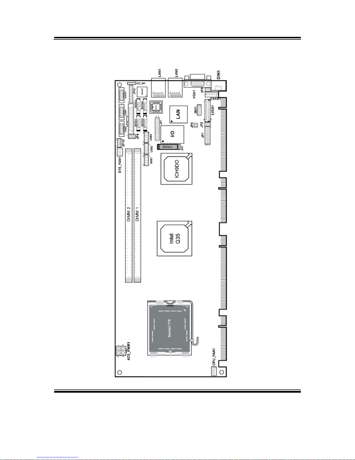
2-2. COMPONENT LOCATIONS
PSB-701LF Connector, Jumper and Component locations
Page 14
Chapter 2 Hardware Configuration
Page: 2-4
PSB-701LF USER
′
S MANUAL
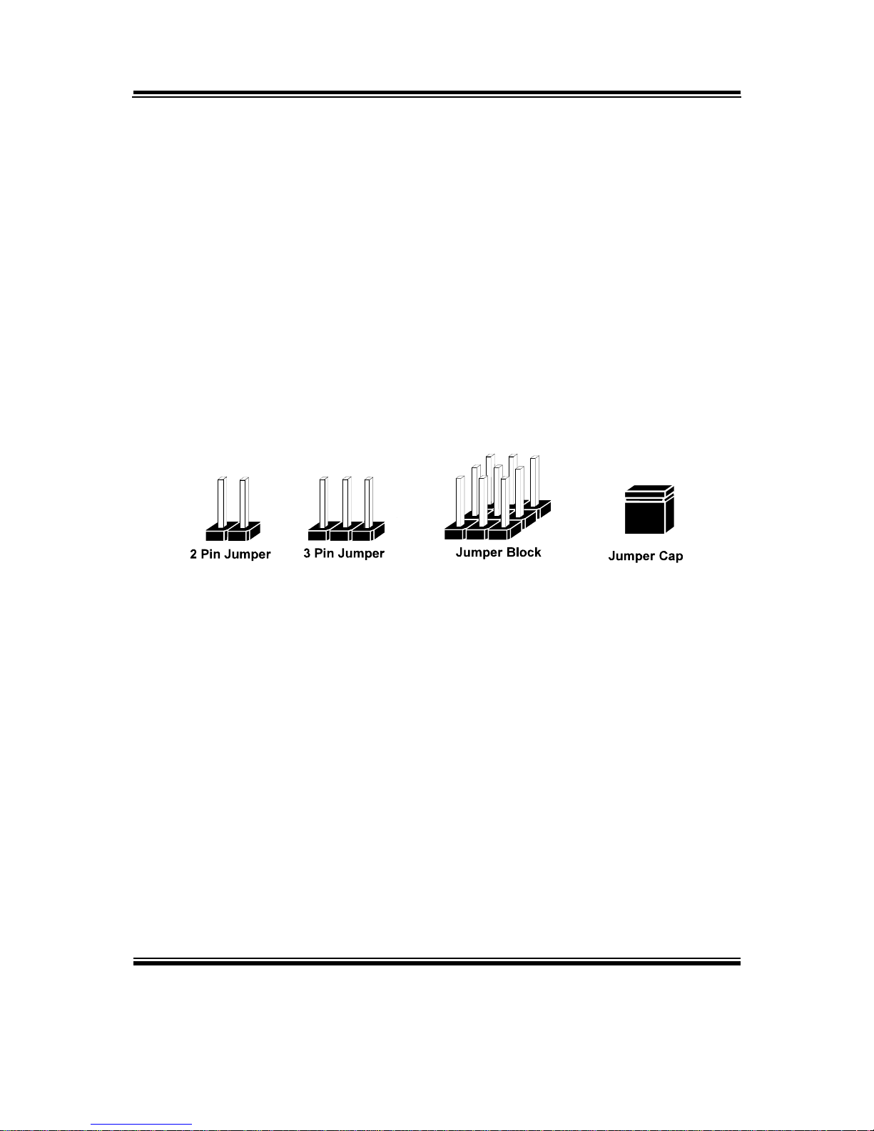
2-3. HOW TO SET THE JUMPERS
You can configure your board by setting jumpers. Jumper is consists of
two or three metal pins with a plastic base mounted on the card, and by
using a small plastic "cap", Also known as the jumper cap (with a metal
contact inside), you are able to connect the pins. So you can set-up your
hardware configuration by "open" or "close" pins.
The jumper can be combined into sets that called jumper blocks. When
the jumpers are all in the block, you have to put them together to set up
the hardware configuration. The figure below shows how this looks like.
JUMPERS AND CAPS
If a jumper has three pins (for examples, labelled PIN1, PIN2, and PIN3),
You can connect PIN1 & PIN2 to create one setting by shorting. You can
either connect PIN2 & PIN3 to create another setting. The same jumper
diagrams are applied all through this manual. The figure below shows
what the manual diagrams look and what they represent.
Page 15
Chapter 2 Hardware Configuration
PSB-701LF USER′S MANUAL
Page: 2-5
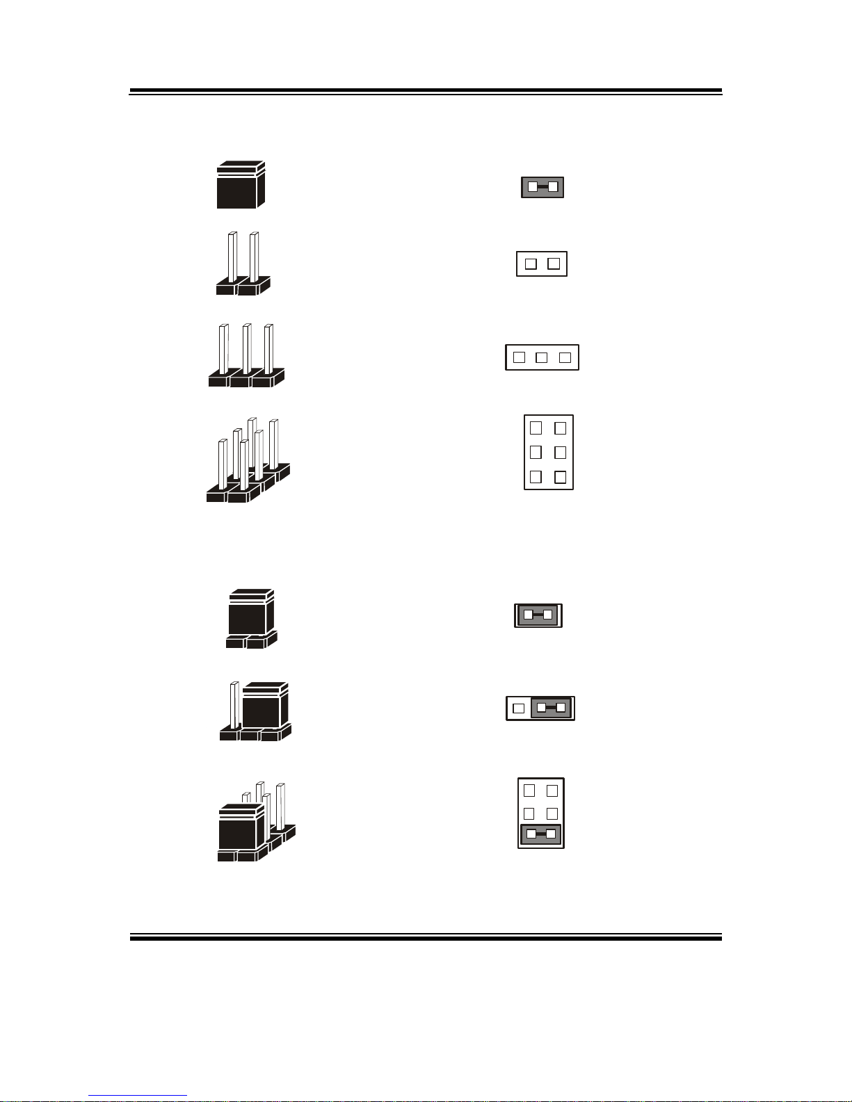
JUMPER DIAGRAMS
2 pin Jumper
looks like this
Jumper Ca p
looks like this
3 pin Jumper
looks like this
Jumper Bl o ck
looks like this
JUMPER SETTINGS
Looks like this
3 pin Jumper
2-3 pin close(ena b led)
Looks like this
Jumper Block
1-2 pin close(ena b led)
2 pin Jumper close(enabled)
1
1
1
2
12
1
1
Looks like this
Page 16
Chapter 2 Hardware Configuration
Page: 2-6
PSB-701LF USER
′
S MANUAL
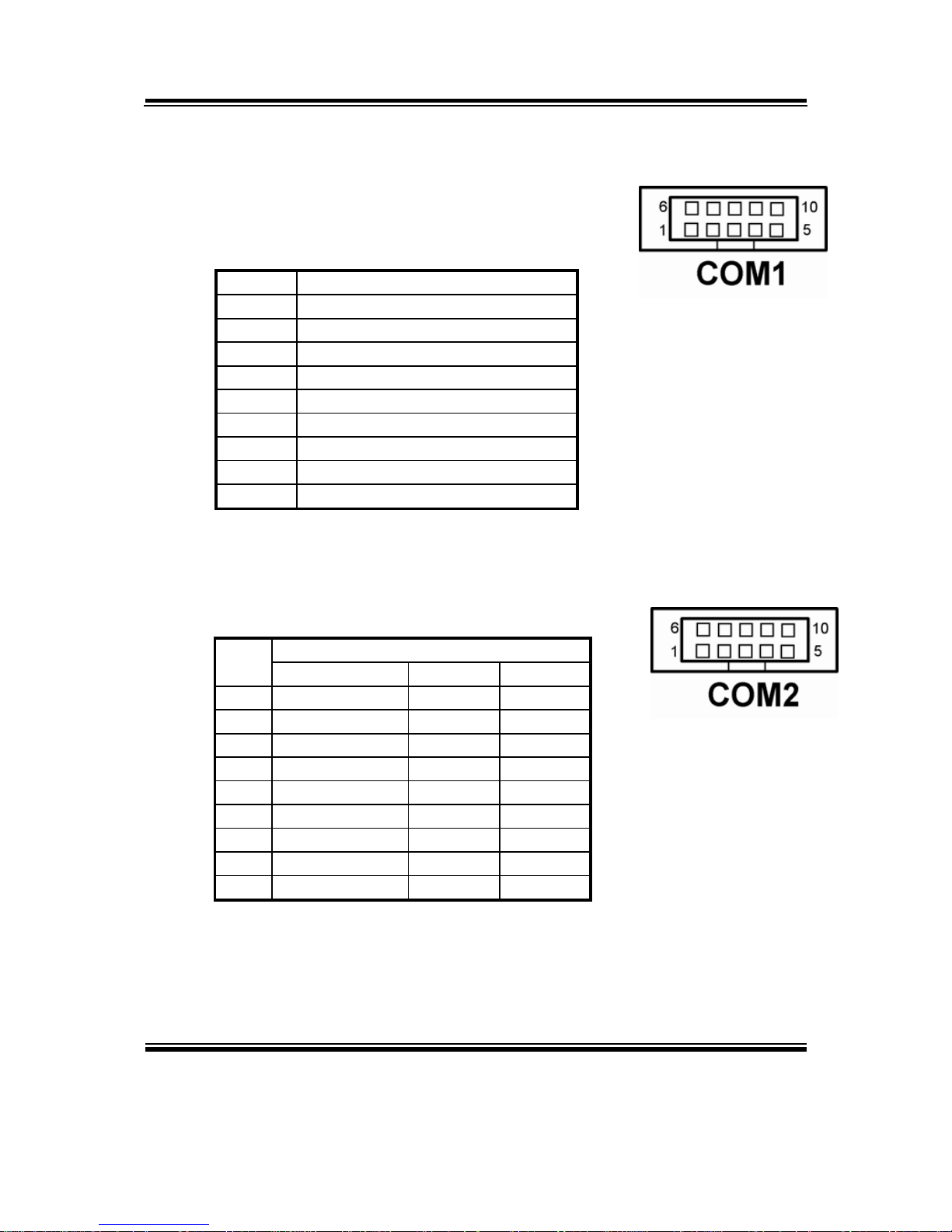
2-4. COM PORT CONNECTOR
COM1 : COM1 Connector
COM1 is fixed as RS-232.
The pin assignment is as follows :
PIN ASSIGNMENT
1 COM1_DCD#
2 COM1_RX
3 COM1_TX
4 COM1_DTR#
5 GND
6 COM1_DSR#
7 COM1_RTS#
8 COM1_CTS#
9 COM1_RI#
COM2 : COM2 Connector
The COM2 is selectable as RS-232/422/485.
The pin assignment is as follows :
ASSIGNMENT
PIN
RS-232 RS-422 RS-485
1 COM2_DCD# TX- TX2 COM2_RX TX+ TX+
3 COM2_TX RX+ RX+
4 COM2_DTR# RX- RX5 GND GND GND
6 COM2_DSR# RTS- GND
7 COM2_RTS# RTS+ GND
8 COM2_CTS# CTS+ GND
9 COM2_RI# CTS- GND
Page 17
Chapter 2 Hardware Configuration
PSB-701LF USER′S MANUAL
Page: 2-7
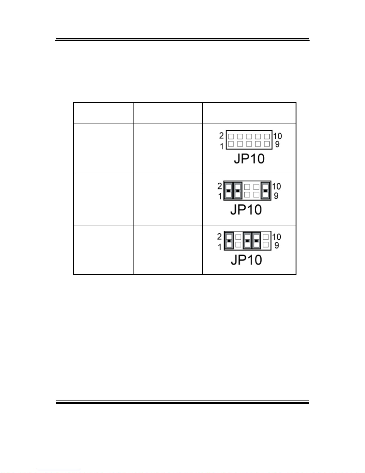
2-5. RS232/422/485 (COM2) SELECTION
JP10 : RS-232/422/485 (COM2) Selection
This connector is used to set the COM2 function.
The jumper settings are as follows :
COM 2
Function
Jumper Settings
(pin closed)
Jumper
Illustrations
RS-232 All Open
RS-422 1-2, 3-4, 9-10
RS-485 1-2, 5-6, 7-8
*** Manufacturing default -- RS-232.
Page 18
Chapter 2 Hardware Configuration
Page: 2-8
PSB-701LF USER
′
S MANUAL
2-6. KEYBOARD AND PS/2 MOUSE CONNECTOR
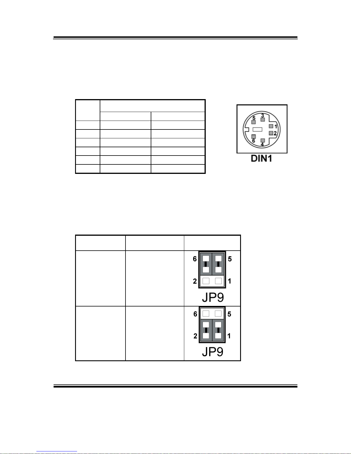
DIN1 : Keyboard or PS/2 Mouse Connector
DIN connector can support keyboard, Y-cable, or PS/2 Mouse, user may
select the right device to used on “Keyboard or PS/2 Mouse Selection”.
The pin assignments are as follows :
ASSIGNMENT
PIN
Keyboard PS/2 Mouse
1 KBDATA MSDATA
2 MSDATA MSDATA
3 GND GND
4 5VSB 5VSB
5 KBCLK MSCLK
6 MSCLK MSCLK
2-7. KEYBOARD OR PS/2 MOUSE SELECTION
JP9 : Keyboard or PS/2 Mouse Selection
For Y-Cable user, please set the jumper same as AT keyboard.
The jumper settings are as follows:
DEVICE TYPE
JUMPER SETTING
(pin closed)
JUMPER
ILLUSTRATION
AT KEYBOARD
3-5
4-6
PS/2 MOUSE
1-3
2-4
*** Manufactory default -- AT Keyboard
Page 19
Chapter 2 Hardware Configuration
PSB-701LF USER′S MANUAL
Page: 2-9
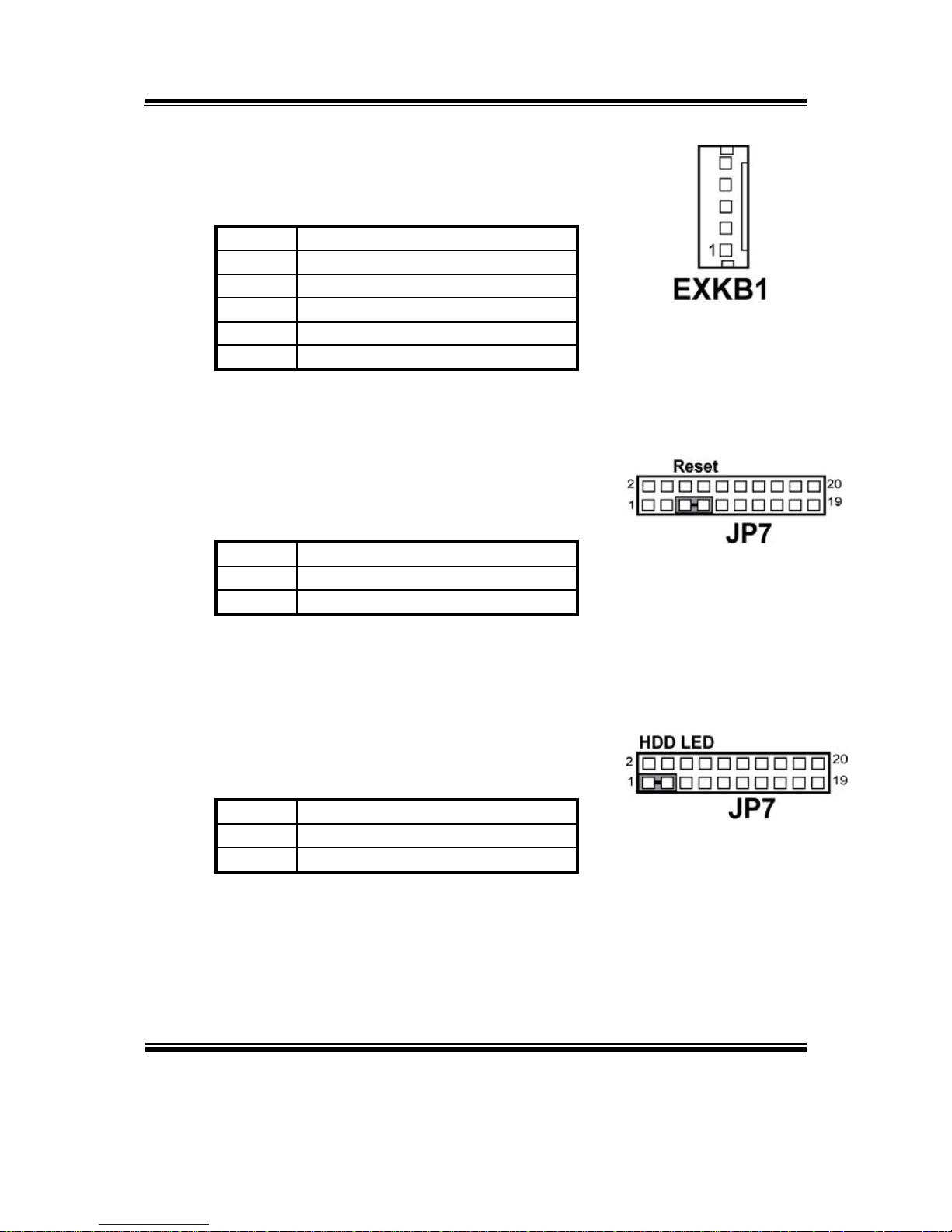
2-8. EXTERNAL KEYBOARD CONNECTOR
EXKB1 : External Keyboard Connector
The pin assignment is as follows :
PIN ASSIGNMENT
1 5VSB
2 GND
3 NC
4 KBDATA
5 KBCLK
2-9. RESET CONNECTOR
JP7 (5, 7) : Reset Connector.
The pin assignment is as follows :
PIN ASSIGNMENT
5 GND
7 RST_BTN
2-10. HARD DISK DRIVE LED CONNECTOR
JP7 (1, 3) : Hard Disk Drive LED Connector
The pin assignment is as follows :
PIN ASSIGNMENT
1 HD_LED+
3 HD_LED-
Page 20
Chapter 2 Hardware Configuration
Page: 2-10
PSB-701LF USER
′
S MANUAL
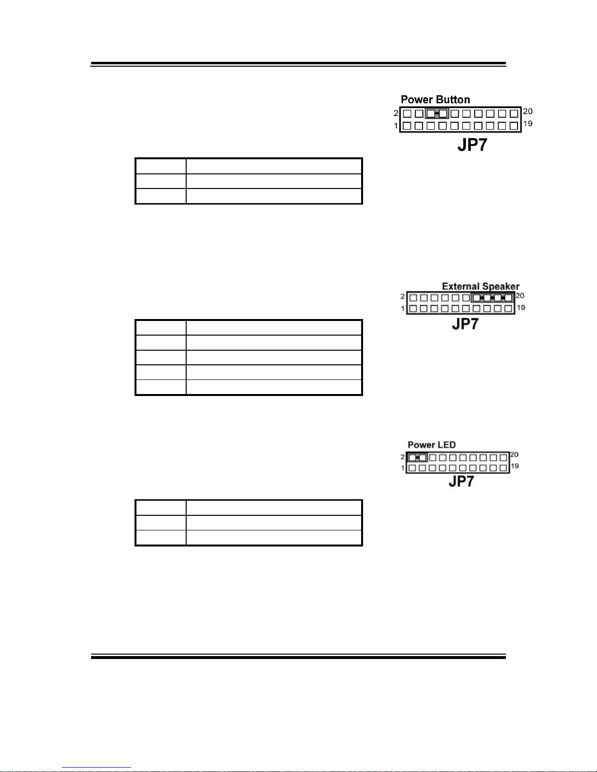
2-11. ATX POWER BUTTON
JP7 (6, 8) : ATX Power Button
The pin assignment is as follows :
PIN ASSIGNMENT
6 PWRBTNSW
8 GND
2-12. EXTERNAL SPEAKER CONNECTOR
JP7 (14, 16, 18, 20) : External Speaker Connector
The pin assignment is as follows :
PIN ASSIGNMENT
14 SPK_VCC
16 SPEAKER SIGNAL
18 SPEAKER SIGNAL
20 SPEAKER SIGNAL
2-13. POWER LED CONNECTOR
JP7 (2, 4) : Power LED Connector
The pin assignment is as follows:
PIN ASSIGNMENT
2 PW_LED+
4 PW_LED-
Page 21

Chapter 2 Hardware Configuration
PSB-701LF USER′S MANUAL
Page: 2-11
2-14. KEYLOCK CONNECTOR
JP7 (13, 15) : Keylock Connector
The pin assignment is as follows:
PIN ASSIGNMENT
13 KEYLOCK
15 GND
2-15. EXTERNAL SMI CONNECTOR
JP7 (17,19) : External SMI Connector
The pin assignment is as follows:
PIN ASSIGNMENT
17 SLP_BTN
19 GND
Page 22

Chapter 2 Hardware Configuration
Page: 2-12
PSB-701LF USER
′
S MANUAL
2-16. CLEAR CMOS DATA SELECTION
JP3 : Clear CMOS Data Selection
The selections are as follows :
FUNCTION
JUMPER SETTING
(pin closed)
JUMPER
ILLUSTRATION
Normal 1-2
Clear CMOS 2-3
*** Manufacturing Default -- Normal.
Note: To clear CMOS data, user must power-off the computer and set the jumper
to “Clear CMOS” as illustrated above. After five to six seconds, set the
jumper back to “Normal” and power-on the computer.
2-17. CPU FAN CONNECTOR
CPU_FAN1 : CPU Fan connector
The pin assignment is as follows:
PIN ASSIGNMENT
1 GND
2 VCC12
3 LPC1_FANIO1
4 LPC1_FANPWM1
Page 23

Chapter 2 Hardware Configuration
PSB-701LF USER′S MANUAL
Page: 2-13
2-18. SYSTEM FAN CONNECTOR
SYS_FAN1 : System Fan connector
The pin assignment is as follows:
PIN ASSIGNMENT
1 GND
2 VCC12
3 LPC1_FANIO2
2-19. INVERTER CONNECTOR
INV1 : Inverter Connector
The pin assignment is as follows:
PIN ASSIGNMENT
1 +12V
2 GND
3 VCC
4 NC
5 ENABKL(Inverter backlight
ON/OFF control signal)
Page 24
Chapter 2 Hardware Configuration
Page: 2-14
PSB-701LF USER
′
S MANUAL
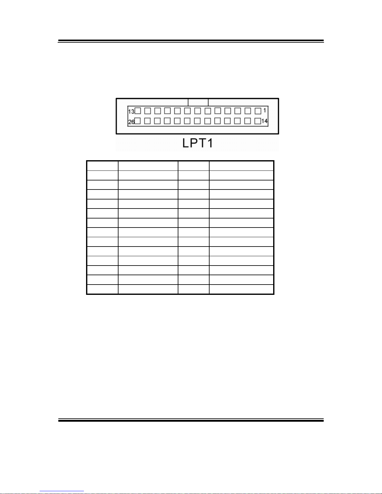
2-20. PRINTER CONNECTOR
LPT1: Printer Connector
As to link the Printer to the card, you need a cable to connect both
DB25 connector and parallel port.
The pin assignments are as follows :
PIN ASSIGNMENT PIN ASSIGNMENT
1 STB 14 AFD#
2 PDR0 15 ERROR#
3 PDR1 16 PAR_INIT#
4 PDR2 17 SLIN#
5 PDR3 18 GND
6 PDR4 19 GND
7 PDR5 20 GND
8 PDR6 21 GND
9 PDR7 22 GND
10 ACK# 23 GND
11 BUSY 24 GND
12 PE 25 GND
13 SLCT 26 NC
Page 25

Chapter 2 Hardware Configuration
PSB-701LF USER′S MANUAL
Page: 2-15
2-21. TPM CONNECTOR
JP12: TPM Connector
PIN ASSIGNMENT PIN ASSIGNMENT
1 LCLK 2 GND
3 LFRAMEJ 4 NC
5 LRESTJ 6 NC
7 LAD3 8 LAD2
9 VCC3_3 10 LAD1
11 LAD0 12 GND
13 NC 14 NC
15 3_3USB 16 SERIRQ
17 GND 18 CLKRUN
19 LPCPDJ 20 NC
Page 26

Chapter 2 Hardware Configuration
Page: 2-16
PSB-701LF USER
′
S MANUAL
2-22. VGA CONNECTOR
VGA1: VGA Connector
PIN ASSIGNMENT
1 GMCH_CRTRED
2 GMCH_GRTGREEN
3 GMCH_CRTBLUE
4 NC
5 GND
6 GND
7 GND
8 GND
9 GMCH_CRTVCC_L
10 GND
11 NC
12 GMCH_CRTDATA
13 GMCH_HSYNC
14 GMCH_VSYNC
15 GMCH_CRTCLK
Page 27

Chapter 2 Hardware Configuration
PSB-701LF USER′S MANUAL
Page: 2-17
2-23. SERIAL ATA CONNECTOR
SATA1, SATA2, SATA3, SATA4 : The PSB-701LF possesses four
Serial ATA Connector. The pin assignments are as follows:
SATA1:
PIN ASSIGNMENT
1 GND
2 SATAHDR_TXP0
3 SATAHDR_TXN0
4 GND
5 SATAHDR_RXN0
6 SATAHDR_RXP0
7 GND
SATA2:
PIN ASSIGNMENT
1 GND
2 SATAHDR_TXP1
3 SATAHDR_TXN1
4 GND
5 SATAHDR_RXN1
6 SATAHDR_RXP1
7 GND
Page 28

Chapter 2 Hardware Configuration
Page: 2-18
PSB-701LF USER
′
S MANUAL
SATA3:
PIN ASSIGNMENT
1 GND
2 SATAHDR_TXP2
3 SATAHDR_TXN2
4 GND
5 SATAHDR_RXN2
6 SATAHDR_RXP2
7 GND
SATA4:
PIN ASSIGNMENT
1 GND
2 SATAHDR_TXP3
3 SATAHDR_TXN3
4 GND
5 SATAHDR_RXN3
6 SATAHDR_RXP3
7 GND
Page 29

Chapter 2 Hardware Configuration
PSB-701LF USER′S MANUAL
Page: 2-19
2-24. UNIVERSAL SERIAL BUS CONNECTOR
USB1: Universal Serial Bus Connector
The pin assignments are as follows:
PIN ASSIGNMENT
1 USB1_VCC5
2 USBN0_L
3 USBP0_L
4 GND
5 NC
6 USB1_VCC5
7 USBN1_L
8 USBP1_L
9 GND
10 NC
USB2: Universal Serial Bus Connector
The pin assignments are as follows:
PIN ASSIGNMENT
1 USB2_VCC5
2 USBN2_L
3 USBP2_L
4 GND
5 NC
6 USB2_VCC5
7 USBN3_L
8 USBP3_L
9 GND
10 NC
Page 30

Chapter 2 Hardware Configuration
Page: 2-20
PSB-701LF USER
′
S MANUAL
USB3: Universal Serial Bus Connector
The pin assignments are as follows:
PIN ASSIGNMENT
1 USB3_VCC5
2 USBN4_L
3 USBP4_L
4 GND
5 NC
6 USB3_VCC5
7 USBN5_L
8 USBP5_L
9 GND
10 NC
Page 31

Chapter 2 Hardware Configuration
PSB-701LF USER′S MANUAL
Page: 2-21
2-25. LAN CONNECTOR
LAN1 : LAN Connector
The pin assignments are as follows:
PIN ASSIGNMENT
1 P1_MDIP0
2 P1_MDIN0
3 P1_MDIP1
4 P1_MDIN1
5 P1_MDIP2
6 P1_MDIN2
7 P1_MDIP3
8 P1_MDIN3
LAN LED Indicator:
Left Side LED
Green Color On 10/100 LAN Speed Indicator
Orange Color On Giga LAN Speed Indicator
Off No LAN switch/ hub connected.
Right Side LED
Yellow Color Blinking LAN Message Active
Off No LAN Message Active
Page 32

Chapter 2 Hardware Configuration
Page: 2-22
PSB-701LF USER
′
S MANUAL
LAN2 : LAN Connector
The pin assignments are as follows:
PIN ASSIGNMENT
1 P2_MDIP0
2 P2_MDIN0
3 P2_MDIP1
4 P2_MDIN1
5 P2_MDIP2
6 P2_MDIN2
7 P2_MDIP3
8 P2_MDIN3
LAN LED Indicator:
Left Side LED
Green Color On 10/100 LAN Speed Indicator
Orange Color On Giga LAN Speed Indicator
Off No LAN switch/ hub connected.
Right Side LED
Yellow Color Blinking LAN Message Active
Off No LAN Message Active
Page 33

Chapter 2 Hardware Configuration
PSB-701LF USER′S MANUAL
Page: 2-23
2-26. ATX POWER CONNECTOR
ATX_PW1 : ATX 12V Connector
The pin assignments are as follows:
PIN ASSIGNMENT
1 GND
2 GND
3 +12V
4 +12V
2-27. MEMORY INSTALLATION
PSB-701LF CPU Card can support up to 4GB in two DIMM sockets.
DRAM BANK CONFIGURATION
DIMM 1 DIMM 2 TOTAL MEMORY
256MB 256MB 512MB
512MB 512MB 1GB
1GB 1GB 2GB
2GB 2GB 4GB
Page 34

Chapter 2 Hardware Configuration
Page: 2-24
PSB-701LF USER
′
S MANUAL
2-28. SOUND CONNECTOR
AUDIO1 : Sound Connector.
The pin assignments are as follows :
PIN ASSIGNMENT
1 AC97_MIC-IN
2 AUDIO_GND
3 AUDIO_GND
4 AUDIO_GND
5 AC97_LINE-L
6 AC97_LINE-R
7 AUDIO_GND
8 AUDIO_GND
9 AC97_SPK-L
10 AC97_SPK-R
2-29. CD AUDIO-IN CONNECTOR
CD_IN1 : CD Audio-In Connector
The pin assignments are as follows:
PIN ASSIGNMENT
1 CD L
2 CDGND
3 CDGND
4 CD R
Page 35

Chapter 2 Hardware Configuration
PSB-701LF USER′S MANUAL
Page: 2-25
2-30. LVDS CONNECTOR
LVDS1 : LVDS Connector.
The pin assignments are as follows:
PIN ASSIGNMENT PIN ASSIGNMENT
1 LVDS_VCC 2 GND
3 CLKBM 4 CLKBP
5 GND 6 YBM2
7 YBP2 8 GND
9 YBM1 10 YBP1
11 YBP3 12 YBM3
13 YBP0 14 YBM0
15 GND 16 CLKAP
17 CLKAM 18 GND
19 YAP2 20 YAM2
21 GND 22 YAP1
23 YAM1 24 GND
25 YAP0 26 YAM0
27 YAP3 28 YAM3
29 LVDS_VCC 30 LVDS_VCC
Page 36

Chapter 2 Hardware Configuration
Page: 2-26
PSB-701LF USER
′
S MANUAL
2-31. LVDS PANEL VOLTAGE SELECTION
JP2 : LVDS Panel Voltage Selection.
The selections are as follows:
FUNCTION
JUMPER SETTING
(pin closed)
JUMPER
ILLUSTRATION
LVDS_VCC3
1-3
2-4
LVDS_VCC5
3-5
4-6
*** Manufactory default --- LVDS_VCC3.
Page 37

Chapter 2 Hardware Configuration
PSB-701LF USER′S MANUAL
Page: 2-27
2-32. PCI EXPRESS / SDVO INTERFACE SELECTION
JP1, JP5 : PCI Express / SDVO Interface Selection
The selections are as follows:
JUMPER SETTING
(pin closed)
SELECTION
JP15 JP16
JUMPER
ILLUSTRATION
PCI Express
open
2-3, 5-6, 8-9,
11-12, 14-15,
17-18, 20-21,
23-24, 26-27,
29-30
SDVO
1-2, 3-4
1-2, 4-5, 7-8,
10-11, 13-14,
16-17, 19-20,
22-23, 25-26,
28-29
*** Manufacturing Default: SDVO
Page 38

Page: 3-1
SOFTWARE
UTILITIES
This chapter comprises the detailed information of VGA driver, LAN
driver, Sound driver, and flash BIOS update. It also describes on how to
configuration the watchdog timer.
Section includes:
z Introduction.
z VGA Driver Utility
z Flash BIOS Update
z LAN Driver Utility
z Sound Driver Utility
z Intel® Chipset Software Installation Utility
z USB2.0 Chipset Software Installation Utility
z Watchdog Timer Configuration
CHAPTER
3
Page 39

Chapter 3 Software Configuration
Page:3-2
PSB-701LF USER
′
S MANUAL
3-1. INTRODUCTION
Enclosed with our PSB-701LF package is our driver utility, which may
comes in a form of a CD ROM disc or floppy diskettes. For CD ROM disc
user, you will only need some of the files contained in the CD ROM disc,
please kindly refer to the following chart:
Filename
(Assume that CD ROM drive is D:)
Purpose
D:\Driver\VGA Intel Q35
For VGA driver installation
D:\Driver\FLASH For BIOS update utility
D:\Driver\LAN For INTEL LAN Driver
installation
D:\Driver\SOUND Realtel ALC262 Audio HD
For Sound driver installation
D:\Driver\UTILITY Intel® Chipset Software
Installation Utility
For Win 2000, XP,VISTA
D:\Driver\RAID\SOFTWARE Intel® ICH9-DO RAID Software
Installation Utility For Win 2000,
XP,VISTA
D:\Driver\USB 2.0 USB 2.0 Software Installation
Utility
For Win 2000, XP
D:\Driver\RAID\DRIVER\F6flpy32 Intel® ICH9-DO driver used for
FLOPPY when Install Win2000,
XP,VISTA
D:\Driver\RAID\DRIVER\F6flpy64 Intel® ICH9-DO driver used for
FLOPPY when Install WinXP-
64,VISTA-64
User should remember to install the Utility right after the OS fully installed.
Page 40

Chapter 3 Software Configuration
PSB-701LF USER′S MANUAL
Page:3-3
3-2. VGA DRIVER UTILITY
The VGA interface embedded with our PSB-701LF can support a wide
range of display. You can display CRT, PCI-E (SDVO) simultaneously
with the same mode.
3-2-1. Installation of VGA Driver:
To install the VGA Driver, simply follow the following steps:
1. Place insert the Utility Disk into Floppy Disk Drive A/B or CD
ROM drive.
2. Under Windows 2000/XP/Vista system, go to the directory where
VGA driver is located.
3. Click Setup.exe file for VGA driver installation.
4. Follow the instructions on the screen to complete the installation.
5. Once installation is completed, shut down the system and restart in
order for the changes to take effect.
Page 41

Chapter 3 Software Configuration
Page:3-4
PSB-701LF USER
′
S MANUAL
3-3. FLASH BIOS UPDATE
3-3-1. System BIOS Update:
Users of PSB-701LF can use the program “
AWDFLASH.EXE” contained in CD
ROM for BIOS update. This is found in
D:\DRIVER\FLASH\AWDFLASH.EXE.
3-3-2. To update BIOS :
(1) Install “
AWDFLASH.EXE” from the CD ROM Disk into your system.
(2) Insert the new BIOS file you have obtained from Protech.
(3) Type the pathname to Awdflash.exe and execute the BIOS update with
file F701xxxx.bin
D:\DRIVER\FLASH\AWDFLASH F701XXXX.BIN
(4) The screen will display the table below:
AwardBIOS Flash Utility V8.89
( C )Phoenix Technologies Ltd. All Rights Reserved
For Broadwater-6A79LP69C-00 DATE : 01/16/2007
Flash Type - SST 49LF008A /3.3V
File Name to Program : F701xxxx.bin
Message : Do You Want To Save BIOS (Y/N)
Page 42

Chapter 3 Software Configuration
PSB-701LF USER′S MANUAL
Page:3-5
If you want to save up the original BIOS, enter “Y ”and press < Enter > .
If you choose “N”, the following table will appear on screen.
AwardBIOS Flash Utility V8.89
( C )Phoenix Technologies Ltd. All Rights Reserved
For Broadwater-6A79LP69C-00 DATE : 01/16/2007
Flash Type - SST 49LF008A /3.3V
File Name to Program : F701xxxx.bin
Message : Press ‘Y’ to Program or ‘N’ to Exit
Select “Y”, and the BIOS will be renewed. When you are refreshing your BIOS,
do not turn off or reset the system, or you will damage the BIOS. After you have
completed all the programming. Please turn off the system. Then the Flash BIOS
is fully implemented.
Page 43

Chapter 3 Software Configuration
Page:3-6
PSB-701LF USER
′
S MANUAL
3-4. LAN DRIVER UTILITY
3-4-1. Introduction
PSB-701LF is enhanced with LAN function that can support various
network adapters. Installation programs for LAN drivers are listed as
follows:
For more details on Installation procedure, please refer to Readme.txt
file found on LAN DRIVER UTILITY.
Page 44

Chapter 3 Software Configuration
PSB-701LF USER′S MANUAL
Page:3-7
3-5. SOUND DRIVER UTILITY
3-5-1. Introduction
The Realtek ALC262 sound function enhanced in this system is fully
compatible with Windows 2000, Windows XP and Windows Vista. Below,
you will find the content of the Sound driver :
3-5-2. Installation Procedure for Windows 2000/XP/Vista
1. From the task bar, click on Start, and then Run.
2. In the Run dialog box, type D:\Sound\path\setup, where
“D:\Sound\pathname” refers to the full path to the source files.
3. Click on the OK button or press the ENTER key.
4. Click on the “Next” and OK prompts as they appear.
5. Reboot the system to complete the driver installation.
Page 45

Chapter 3 Software Configuration
Page:3-8
PSB-701LF USER
′
S MANUAL
3-6. INTEL® C HIPSET SOFTWARE INSTALLATION UTILITY
3-6-1. Introduction
The Intel® Chipset Software Installation Utility installs to the target
system the Windows* INF files that outline to the operating system how
the chipset components will be configured. This is needed for the
proper functioning of the following features:
- Core PCI and ISAPNP Services
- AGP Support
- IDE/ATA33/ATA66/ATA100 Storage Support
- USB Support
- Identification of Intel® Chipset Components in Device Manager
3-6-2. Installation of Utility for Windows 2000/XP/Vista
The Utility Pack is to be installed only for Windows 2000 and XP
program.
It should be installed right after the OS installation, kindly follow the
following steps:
1. Place insert the Utility Disk into Floppy Disk Drive A/B or CD
ROM drive.
2. Under Windows 2000/XP/Vista system, go to the directory where
Utility Disc is located.
3. Click Setup.exe file for utility installation.
4. Follow the instructions on the screen to complete the installation.
5. Once installation is completed, shut down the system and restart in
order for the changes to take effect.
Page 46

Chapter 3 Software Configuration
PSB-701LF USER′S MANUAL
Page:3-9
3-7. USB2.0 SOFTWARE INSTALLATION UTILITY
3-7-1. Installation of Utility for Windows 2000/XP
Intel USB 2.0 Enhanced Host Controller driver can only be used on
Windows 2000 and Windows XP on Intel Desktop boards. It should be
installed right after the OS installation, kindly follow the followin g steps:
1. Place insert the Utility Disk into Floppy Disk Drive A/B or CD
ROM drive.
2. Under Windows 2000, and XP system, go to the directory where
Utility Disc is located.
3. Start the “System” wizard in control panel. (Click
Start/Settings/Control Panel).
4. Select “Hardware” and click “Device Manager ” button.
5. Double Click “USB Root Hub”.
6. Select “Driver”.
7. Click “Install” to install the driver.
8. Follow the instructions on the screen to complete the installation.
9. Click “Finish” after the driver installation is complete.
Page 47

Chapter 3 Software Configuration
Page:3-10
PSB-701LF USER
′
S MANUAL
3-7. WATCHDOG TIMER CONFIGURATION
This board has watchdog timer function for monitoring whether the system
is still work or not after a period of time. The user can select watchdog
timer to system reset or NMI (Non Maskable interrupt). This is defined at
I/O port 444H and 448H. When you want to enable the watchdog timer,
please write I/O port 444H and 448H, then the system will either reset itself
or perform the NMI function. If you want to stop watchdog timer, you can
read I/O port 440H, then timer will stop count.
In PSB-701LF watchdog function, You must write your program so when it
writes I/O port address 444H and 448H for enable watchdog. The timer's
intervals have a tolerance of 25% so you should program an instruction that
will refresh the timer about every second.
The following program shows you how to program the watch timer in your
program.
Watchdog of system reset enable program:
MOV AX, 0FH (choose the values you need; start from 0)
MOV DX, 0444H
OUT DX, AX
Watchdog of NMI enable program:
MOV AX, 0FH (choose the values you need; start from 0)
MOV DX, 0448H
OUT DX, AX
Stop Watchdog Timer program:
MOV DX, 0440H
In AX , DX
The Watchdog Timer control table is as follows:
Level Value Time/sec Level Value Time/sec
1 F 0 9 7 64
2 E 8 10 6 72
3 D 16 11 5 80
4 C 24 12 4 88
5 B 32 13 3 96
6 A 40 14 2 104
7 9 48 15 1 112
8 8 56 16 0 120
Page 48

Page: 4-1
AWARD
BIOS SETUP
This chapter shows how to set up the Award BIOS.
Section includes:
z Introduction
z Entering Setup
z The Standard CMOS Features
z The Advanced BIOS Features
z The Advanced Chipset Features
z Integrated Peripherals
z Power Management Setup
z PC Health Status
z Frequency Control
z Load Fail-Safe Defaults
z Load Optimized Defaults
z Password Setting
z Save and Exit Setup
z Exit Without Saving
CHAPTER
4
Page 49

Chapter 4 Award BIOS Setup
Page: 4-2
PSB-701LF USER
′
S MANUAL
4-1. INTRODUCTION
This chapter will show you the function of the BIOS in managing the
features of your system. The PSB-701LF Intel Core 2 Duo/Quad Full Size
CPU Card is equipped with the BIOS for system chipset from Phoenix Award Software Inc. This page briefly explains the function of the BIOS in
managing the special features of your system. The following pages describe
how to use the BIOS for system chipset Setup menu.
Your application programs (such as word processing, spreadsheets, and
games) rely on an operating system such as DOS or OS/2 to manage such
things as keyboard, monitor, disk drives, and memory.
The operating system relies on the BIOS (Basic Input and Output system), a
program stored on a ROM (Read-only Memory) chip, to initialize and
configure your computer's hardware. As the interface between the hardware
and the operating system, the BIOS enables you to make basic changes to
your system's hardware without having to write a new operating system.
The following diagram illustrates the interlocking relationships between the
system hardware, BIOS, operating system, and application program:
Page 50

Chapter 4 Award BIOS Setup
PSB-701LF USER′S MANUAL
Page: 4-3
4-2. ENTERING SETUP
When the system is powered on, the BIOS will enter the Power-On Self
Test (POST) routines and the following message will appear on the lower
screen:
PRESS <DEL> TO ENTER SETUP, ESC TO SKIP MEMORY TEST
As long as this message is present on the screen you may press the <Del>
key (the one that shares the decimal point at the bottom of the number
keypad) to access the Setup program. In a moment, the main menu of the
Award SETUP program will appear on the screen:
Phoenix - AwardBIOS CMOS Setup Utility
►Standard CMOS Features
►Advanced BIOS Features
►Advanced Chipset Features
►Integrated Peripherals
►Power Management Setup
►PC Health Status
Load Fail-Safe Defaults
Load Optimized Defaults
Set Supervisor Password
Set User Password
Save & Exit Setup
Exit Without Saving
Esc : Quit ↑↓→← : Select Item
F10 : Save & Exit Setup
Time, Date, Hard Disk Type .…
Setup program initial screen
You may use the cursor the up/down keys to highlight the individual menu
items. As you highlight each item, a brief description of the highlighted
selection will appear at the bottom of the screen.
Page 51

Chapter 4 Award BIOS Setup
Page: 4-4
PSB-701LF USER
′
S MANUAL
4-3. THE STANDARD CMOS FEATURES
Highlight the〝STANDARD CMOS FEATURES〞and press the <ENTER>
key and the screen will display the following table:
Phoenix - AwardBIOS CMOS Setup Utility
Standard CMOS Features
Date (mm:dd:yy)
Time (hh:mm:ss)
Mon, Jan
1 2007
0 : 5 : 4
Item Help
▶ IDE Channel 0 Master
▶ IDE Channel 0 Slave
▶ IDE Channel 1 Master
▶ IDE Channel 1 Slave
▶ IDE Channel 2 Master
▶ IDE Channel 3 Master
Drive A
Halt On
Base Memory
Extended Memory
Total Memory
[ ST3120026AS]
[ ST3120026AS]
[ None]
[ None]
[PIONEER DVD-ROM DVE-]
[None]
[None]
[All Errors]
639K
496640K
497664K
Menu Level ►
Change the day,
month, year and
century
↑↓→←: Move Enter: Select +/-/PU/PD:Value F10:Save ESC:Exit F1:General Help
F5: Previous Values F6: Fail-Safe Defaults F7:Optimized Defaults
CMOS Setup screen
In the above Setup Menu, use the arrow keys to highlight the item and then use
the <PgUp> or <PgDn> keys to select the value you want in each item.
DATE:
< Month >, < Date > and <Year >. Ranges for each value are in the CMOS
Setup Screen, and the week-day will skip automatically.
TIME:
< Hour >, < Minute >, and < Second >. Use 24 hour clock format, i.e., for PM
numbers, add 12 to the hour. For example: 4: 30 P.M. You should enter the
time as 16:30:00.
Page 52

Chapter 4 Award BIOS Setup
PSB-701LF USER′S MANUAL
Page: 4-5
IDE CHANNEL 0/1 MASTER/ SLAVE,
IDE CHANNEL 2/3 MASTER:
The BIOS can automatically detect the specifications and optimal operating
mode of almost all SATA hard drives. When you select type AUTO for a
hard drive, the BIOS detect its specifications during POST, every time system
boots.
If you do not want to select drive type AUTO, other methods of selecting
drive type are available:
1. Match the specifications of your installed SATA hard drive(s) with
the preprogrammed values for hard drive types 1 through 45.
2. Select USER and enter values into each drive parameter field.
3. Use the SATA HDD AUTO DETECTION function in Setup.
Here is a brief explanation of drive specifications:
Type: The BIOS contains a table of pre-defined drive types. Each
defined drive type has a specified number of cylinders, number of heads,
write precompensation factor, landing zone, and number of sectors.
Drives whose specifications do not accommodate any predefine type are
classified as type USER.
• Size: Disk drive capacity (approximate). Note that this size is usually
greater than the size of a formatted disk given by a disk-checking
program.
• Cyls: number of cylinders.
• Head: number of heads.
• Precomp: write precompensation cylinders.
• Landz: landing zone.
• Sector: number of sectors.
• Mode: Auto, Normal, Large or LBA.
Auto: The BIOS automatically determines the optimal mode.
Normal: Maximum number of cylinders, heads, sectors
supported are 1024, 16 and 63.
Large: For drives that do not support LBA and have more
than 1024 cylinders.
Page 53

Chapter 4 Award BIOS Setup
Page: 4-6
PSB-701LF USER
′
S MANUAL
LBA (Logical Block Addressing): During drive accesses, the
SATA controller transforms the data address described by
sector, head and cylinder number into a physical block
address, significantly improving data transfer rates. For
drives greater than 1024 cylinders.
HALT ON:
This category allows user to choose whether the computer will stop if an error
is detected during power up. Available options are “All errors”, “No errors”,
and “All, But keyboard”.
BASE MEMORY:
Displays the amount of conventional memory detected during boot up.
EXTENDED MEMORY:
Displays the amount of extended memory detected during boot up.
TOTAL MEMORY:
Displays the total memory available in the system.
Page 54

Chapter 4 Award BIOS Setup
PSB-701LF USER′S MANUAL
Page: 4-7
4-4. THE ADVANCED BIOS FEATURES
Choose the〝ADVANCED BIOS FEATURES〞in the main menu, the screen
shown as below.
Phoenix - AwardBIOS CMOS Setup Utility
Advanced BIOS Features
Item Help
▶ Hard Disk Boot Priority
First Boot Device
Second Boot Device
Third Boot Device
Boot Other Device
Security Option
APIC Mode
MPS Version Control For OS
Console Redirection
X Baud Rate
Agent after boot
[Press Enter]
[Hard Disk]
[CDROM]
[LS120]
[Enabled]
[Setup]
[Enabled]
[1.4]
Disabled
19200
Enabled
Menu Level ►
↑↓→←: Move Enter: Select +/-/PU/PD:Value F10:Save ESC:Exit F1:General Help
F5: Previous Values F6: Fail-Safe Defaults F7:Optimized Defaults
BIOS Features Setup Screen
The “BIOS FEATURES SETUP” allow you to configure your system for
basic operation. The user can select the system’s boot-up sequence and
security.
A brief introduction of each setting is given below.
Page 55

Chapter 4 Award BIOS Setup
Page: 4-8
PSB-701LF USER
′
S MANUAL
HARD DISK BOOT PRIORITY:
The options for these items are found in its sub menu. By pressing the
<ENTER> key, you are prompt to enter the sub menu of the detailed options
as shown below:
Phoenix – Award CMOS Setup Utility
Hard Disk Boot Priority
Item Help
1. Ch0 M. : ST3120026AS
2. Ch0 S. : ST3120026AS
3. Bootable Add-in Cards
Menu Level ►
Use<Ç> or <È> to select a
device, then press <+> to move
it up, or <-> to move it down
the list. Press <ESC> to exit
this menu.
↑↓→←:Move Enter: Select +/-/PU/PD:Value F10:Save ESC:Exit F1:General Help
F5: Previous Values F6:Fail-Safe Defaults F7:Optimized Defaults
Select Hard Disk Boot Device Priority
FIRST/SECOND/ THIRD/ OTHER BOOT DEVICE:
The BIOS attempt to load the operating system from the devices in the
sequence selected in these items.
SECURITY OPTION:
This category allows you to limit access to the system and Setup, or just to
Setup.
System The system will not boot and access to Setup will be
denied if the correct password is not entered at the
prompt.
Setup The system will boot, but access to Setup will be
denied if the correct password is not entered at the
prompt.
To disable security, select PASSWORD SETTING at Main Menu and
then you will be asked to enter password. Do not type anything and just
press <Enter>, it will disable security. Once the security is disabled, the
system will boot and you can enter Setup freely.
Page 56

Chapter 4 Award BIOS Setup
PSB-701LF USER′S MANUAL
Page: 4-9
APIC MODE:
To Enable Advanced Programmable Interrupt Controller
MPS VERSION CONTROL FOR OS:
This option is only valid for multiprocessor motherboards as it specifies the
version of the Multiprocessor Specification (MPS) that the motherboard will
use. The MPS is a specification by which PC manufacturers design and build
Intel architecture systems with two or more processors.
4-5. ADVANCED CHIPSET FEATURES
Choose the〝ADVANCED CHIPSET FEATURES〞from the main menu,
the screen shown as below.
Phoenix - AwardBIOS CMOS Setup Utility
Advanced Chipset Features
Item Help
DRAM Timing Selectable
X CAS Latency Time
X DRAM RAS# to CAS# Delay
X DRAM RAS# Precharge
X Precharge dealy (tRAS)
X System Memory Frequency
VT-d
AMT BIOS Support
GbE LAN
SOL Support
IDE-R Support
Platform Mng Selection
** VGA Setting **
DVMT Mode
DVMT/ FIXED Memory Size
PCI SERR# NMI
[By SPD]
Auto
Auto
Auto
Auto
By SPD
[Disabled]
[Enabled]
[Enabled]
Enabled
Enabled
Intel AMD
[DVMT]
[128 MB]
[Disabled]
Menu Level ►
↑↓→←: Move Enter: Select +/-/PU/PD:Value F10:Save ESC:Exit F1:General Help
F5: Previous Values F6: Fail-Safe Defaults F7:Optimized Defaults
Chipset Features Setup Screen
This parameter allows you to configure the system based on the specific
features of the installed chipset. The chipset manages bus speed and
access to system memory resources, such as DRAM and the external cache.
Page 57

Chapter 4 Award BIOS Setup
Page: 4-10
PSB-701LF USER
′
S MANUAL
It also coordinates communications between conventional ISA bus and the
PCI bus. It must be stated that these items should never need to be altered.
The default settings have been chosen because they provide the best operating conditions for the system. The only time you might consider making
any changes would be if you discovered that data was being lost while
using your system.
DRAM TIMEING SELECTABLE:
The value in this field depends on performance parameters of the installed
memory chips (DRAM). Do not change the value from the factory setting
unless you install new memory that has a different performance rating than
the original DRAMs.
CAS LATENCY TIME:
When synchronous DRAM is installed, the number of clock cycles of CAS
latency depends on the DRAM timing.
DRAM RAS# TO CAS# DELAY:
This item let you insert a timing delay between the CAS and RAS strobe
signals, used when DRAM is written to, read from, or refreshed. Fast
gives faster performance; and Slow gives more stable performance. This
field applies only when synchronous DRAM is installed in the system.
The choices are 2 and 3.
DRAM RAS# PRECHARGE TIME:
If an insufficient number of cycles is allowed for the RAS to accumulate its
charge before DRAM refresh, the refresh may be incomplete and the DRAM
may fail to retain data. Fast gives faster performance; and Slow gives more
stable performance. This field applies only when synchronous DRAM is
installed in the system. The choices are 2 & 3.
PRECHARGE DEALY (tRAS):
Precharge Delay This setting controls the precharge delay, which
determines the timing delay for DRAM precharge
SYSTEM MEMORY FREQUENCY:
Allow to choose different frequency of memory module.
VT-d:
Intel Virtualization Technology for Directed I/O.
Page 58

Chapter 4 Award BIOS Setup
PSB-701LF USER′S MANUAL
Page: 4-11
AMT BIOS SUPPORT:
Support Intel Active Management Technology.
GbE LAN:
Control onboard Lan.
SOL SUPPORT:
The message show enable or disable Serial Over Lan.
IDR-R SUPPORT:
The message show enable or disable IDE Redirection.
PLATFORM MNG SELECTION:
The message shows which managed function user choose.
DVMT MODE:
Intel Dynamic Video Memory Technology Mode.
DVMT/FIXED MEMORY SIZE:
DVMT Memory Size Select.
PCI SERR# NMI
To Enable/Disable the PCI SERR# interrupt
Page 59

Chapter 4 Award BIOS Setup
Page: 4-12
PSB-701LF USER
′
S MANUAL
4-6. INTEGRATED PERIPHERALS
Choose〝INTEGRATED PERIPHERALS〞from the main setup menu, a
display will be shown on screen as below:
Phoenix - AwardBIOS CMOS Setup Utility
Integrated Peripherals
Item Help
X OnChip IDE Device
X SuperIO Device
X USB Device Setting
Onboard Lan2 Controller
[Press Enter]
[Press Enter]
[Press Enter]
[Enabled]
Menu Level ►
↑↓→←: Move Enter: Select +/-/PU/PD:Value F10:Save ESC:Exit F1:General Help
F5: Previous Values F6: Fail-Safe Defaults F7:Optimized Defaults
Integrated Peripherals Setup Screen
By moving the cursor to the desired selection and by pressing the <F1> key,
the all options for the desired selection will be displayed for choice.
If bios setup menu item supports USB device boot, it will cause Win9x detects
the same storages twice when the system is rebooted, and USB HDD will fail.
Note: this cause just happen under Win9x, the phenomenon is a limitation.
Page 60

Chapter 4 Award BIOS Setup
PSB-701LF USER′S MANUAL
Page: 4-13
ONCHIP IDE DEVICE:
The options for these items are found in its sub menu. By pressing the
<ENTER> key, you are prompt to enter the sub menu of the detailed options
as shown below:
Phoenix – Award CMOS Setup Utility
OnChip IDE Device
Item Help
SATA Mode
LEGACY Mode Support
[IDE]
[Enabled]
Menu Level ►
↑↓→←:Move Enter: Select +/-/PU/PD:Value F10:Save ESC:Exit F1:General Help
F5: Previous Values F6:Fail-Safe Defaults F7:Optimized Defaults
Descriptions on each item above are as follows:
1. SATA MODE
Set the Serial ATA configuration. When set in Advanced Host
Controller Interface (AHCI) or RAID mode, the SATA controller is set
to Native mode. Configuration options: [IDE] [RAID] [AHCI]
2. LEGACY MODE SUPPORT
Certain OS (Windows 9X/ME) is not supported under Native mode
Page 61

Chapter 4 Award BIOS Setup
Page: 4-14
PSB-701LF USER
′
S MANUAL
SUPER IO DEVICE:
The options for these items are found in its sub menu. By pressing the
<ENTER> key, you are prompt to enter the sub menu of the detailed options
as shown below:
Phoenix – Award CMOS Setup Utility
SuperIO Device
Item Help
Onboard Serial Port 1
Onboard Serial Port 2
Onboard Parallel Port
Parallel Port Mode
X ECP Mode Use DMA
PWRON After PWR-Fail
[3F8/IRQ4]
[2F8/IRQ3]
[378/IRQ7]
[SPP]
3
[On]
Menu Level ►
↑↓→←:Move Enter: Select +/-/PU/PD:Value F10:Save ESC:Exit F1:General Help
F5: Previous Values F6:Fail-Safe Defaults F7:Optimized Defaults
Descriptions on each item above are as follows:
1. ONBOARD SERIAL PORT 1/2
Select an address and corresponding interrupt for the first and second
serial ports.
2. ONBOARD PARALLEL PORT
This item allows you to determine access onboard parallel port
controller with which I/O address.
3. PARALLEL PORT MODE
Select an operating mode for the onboard parallel (printer) port.
Select Normal, Compatible, or SPP unless you are certain your
hardware and software both support one of the other available modes.
4. ECP MODE USE DMA
Select a DMA channel for the parallel port for use during ECP mode.
5. PWRON AFTER PWR-FAIL
This item allows you to select if you want to power on the system after
power failure. The choice:Off,On,Former-Sts.
Page 62

Chapter 4 Award BIOS Setup
PSB-701LF USER′S MANUAL
Page: 4-15
USB DEVICE SETTING:
The options for these items are found in its sub menu. By pressing the
<ENTER> key, you are prompt to enter the sub menu of the detailed options
as shown below:
Phoenix – Award CMOS Setup Utility
Onboard Device
Item Help
USB 1.0 Controller
USB 2.0 Controller
USB Keyboard Function
USB Storage Function
*** USB Mass Storage Device Boot
JetFlashTS4GJFV20 0.00
[Enabled]
[Enabled]
[Enabled]
[Enabled]
Setting ***
[Auto mode]
Menu Level ►
[Enable] or [Disable]
Universal Host
Controller
Interfacefor Universal
Serial Bus.
↑↓→←:Move Enter: Select +/-/PU/PD:Value F10:Save ESC:Exit F1:General Help
F5: Previous Values F6:Fail-Safe Defaults F7:Optimized Defaults
Descriptions on each item above are as follows:
1. USB 1.0 CONTROLLER
This should be enabled if your system has a USB installed on the
system board and you want to use it. Even when so equipped, if you
add a higher performance controller, you will need to disable this
feature.
2. USB 2.0 CONTROLLER
Enable the USB 2.0 controller.
3. USB KEYBOARD FUNCTION
Select Enabled if your system contains a Universal Serial Bus (USB)
controller and you have a USB keyboard.
4. USB STORAGE FUNCTION
Enable the USB Storage Function
5. USB MASS STORAGE DEVICE BOOT
[Auto]: According to contents of USB MSD decide boot up type
[FDD Mode]: The USB MSD always boot up as floppy disk
'[HDD Mode]: The USB MSD always boot up as hard disk.
ONBOARD LAN 2 CONTROLLER:
Enable the LAN controller.
Page 63

Chapter 4 Award BIOS Setup
Page: 4-16
PSB-701LF USER
′
S MANUAL
4-7. POWER MANAGEMENT SETUP
Choose〝POWER MANAGEMENT SETUP〞option on the main menu, a
display will be shown on screen as below :
Phoenix - AwardBIOS CMOS Setup Utility
Power Management Setup
[Enabled]
[S3 (STR)]
[Instant-Off]
[Enabled]
Item Help
ACPI Function
ACPI Suspend Type
Soft-Off by PWR-BTTN
PME Event Wake Up
Menu Level ►
↑↓→←: Move Enter: Select +/-/PU/PD:Value F10:Save ESC:Exit F1:General Help
F5: Previous Values F6: Fail-Safe Defaults F7:Optimized Defaults
Power Management Setup Screen
The “Power Management Setup” allows the user to configure the system to
the most effectively save energy while operating in a manner consistent with
your own style of computer use.
ACPI FUNCTION:
Users are allowed to enable or disable the Advanced Configuration and
Power Management (ACPI).
ACPI SUSPEND TYPE:
User can choose S1 (Power On Suspend) or S3 (Suspend To Ram)
SOFT-OFF BY PWR-BTTN:
Pressing the power button for more than 4 seconds forces the system to
enter the Soft-Off state when the system has “hung”. The choices are
Delay 4 Sec and Instant-Off.
PME EVENT WAKE UP:
An input signal PME wake the system from the soft-off state
Page 64

Chapter 4 Award BIOS Setup
PSB-701LF USER′S MANUAL
Page: 4-17
4-8. PC HEALTH STATUS
Choose 〝PC HEALTH STATUS〞 from the main menu, a display will
be shown on screen as below:
Phoenix - AwardBIOS CMOS Setup Utility
PC Health Status
Item Help
Shutdown Temperature
Vcore
+1.8V
+3.3V
+12V
+5V
System Temperature
CPU Temperature
CPU FAN
System FAN
[Enabled]
1.28V
1.79V
3.34V
12.223V
4.94V
35 C
29 C
4687 RPM
0 RPM
Menu Level ►
↑↓→←: Move Enter: Select +/-/PU/PD:Value F10:Save ESC:Exit F1:General Help
F5: Previous Values F6: Fail-Safe Defaults F7:Optimized Defaults
PC Health Status Setup Screen
The PC Health Status Setup allows you to select whether to choose between
monitoring or to ignore the hardware monitoring function of your system.
SHUTDOWN TEMPERATURE:
This item allows you to set up the CPU shutdown Temperature.
VCORE:
This item shows you the current system voltage.
1.8V/3.3V/12V / 5V :
Show you the voltage of 1.8V/3.3V/12V/5V.
SYSTEM/CPU TEMPERATURE:
This item shows you the current System/CPU temperature.
CPU/SYSTEM/POWER FAN:
This item shows you the current CPU/ SYSTEM /Power FAN speed.
Page 65

Chapter 4 Award BIOS Setup
Page: 4-18
PSB-701LF USER
′
S MANUAL
4-9. LOAD FAIL-SAFE DEFAULTS
By pressing the <ENTER> key on this item, you get a confirmation dialog
box with a message similar to the following:
Load Fail-Safe Defaults ( Y/N ) ? N
To use the BIOS default values, change the prompt to "Y" and press the
<Enter > key. CMOS is loaded automatically when you power up the
system.
4-10. LOAD OPTIMIZED DEFAULTS
When you press <Enter> on this category, you get a confirmation dialog
box with a message similar to the following:
Load Optimized Defaults ( Y/N ) ? N
Pressing "Y" loads the default values that are factory setting for optimal
performance system operations.
Page 66

Chapter 4 Award BIOS Setup
PSB-701LF USER′S MANUAL
Page: 4-19
4-11. PASSWORD SETTING
User is allowed to set either supervisor or user password, or both of them.
The difference is that the supervisor password can enter and change the
options of the setup menus while the user password can enter only but do not
have the authority to change the options of the setup menus.
TO SET A PASSWORD
When you select this function, the following message will appear at the
center of the screen to assist you in creating a password.
Enter Password:
Type the password up to eight characters in length, and press < Enter >.
The password typed now will clear any previously entered password from
CMOS memory. You will be asked to confirm the password. Type the
password again and press the < Enter > key. You may also press < Esc >
to abort the selection and not enter a password.
User should bear in mind that when a password is set, you will be
asked to enter the password everything you enter CMOS setup Menu.
TO DISABLE THE PASSWORD
To disable the password, select this function (do not enter any key when
you are prompt to enter a password), and press the <Enter> key and a
message will appear at the center of the screen:
PASSWORD DISABLED!!!
Press any key to continue...
Press the < Enter > key again and the password will be disabled. Once the
password is disabled, you can enter Setup freely.
Page 67

Chapter 4 Award BIOS Setup
Page: 4-20
PSB-701LF USER
′
S MANUAL
4-12. SAVE & EXIT SETUP
After you have completed adjusting all the settings as required, you must
remember to save these setting into the CMOS RAM. To save the settings,
select “SAVE & EXIT SETUP” and press <Enter>, a display will be shown
as follows:
Phoenix - AwardBIOS CMOS Setup Utility
►Standard CMOS Features
►Advanced BIOS Features
►Advanced Chipset Features
►Integrated Peripherals
►Power Management
►PC Health Status
Load Fail-Safe Defaults
Load Optimized Defaults
Set Supervisor Password
word
etup
Saving
Esc : Quit ↑↓→← : Select Item
F10 : Save & Exit Setup
Save Data to CMOS
When you confirm that you wish to save the settings, your system will be
automatically restarted and the changes you have made will be implemented.
You may always call up the setup program at any time to adjust any of the
individual items by pressing the <Del> key during boot up.
Save to CMOS and EXIT Y/N)? Y
Page 68

Chapter 4 Award BIOS Setup
PSB-701LF USER′S MANUAL
Page: 4-21
4-13. EXIT WITHOUT SAVING
If you wish to cancel any changes you have made, you may select the
“EXIT WITHOUT SAVING” and the original setting stored in the CMOS
will be retained. The screen will be shown as below:
Phoenix - AwardBIOS CMOS Setup Utility
►Standard CMOS Features
►Advanced BIOS Features
►Advanced Chipset Features
►Integrated Peripherals
►Power Management
►PC Health Status
Load Fail-Safe Defaults
Load Optimized Defaults
Set Supervisor Password
word
etup
Saving
Esc : Quit ↑↓→← : Select Item
F10 : Save & Exit Setup
Abandon all Datas
Quit Without Saving (Y/N)? N
Page 69

Page: A-1
EXPANSION BUS
This appendix indicates the pin assignments.
Section includes:
z SHB Connector Pin Assignment
APPENDIX
A
Page 70

Appendix A Expansion Bus
Page: A-2
PSB-701LF USER
′
S MANUAL
SHB CONNECTOR PIN ASSIGNMENT
The following table shows pin assignments for the PCI Express edge connectors:
Connector A Connector B Connector C Connector D
Side B Side A Side B Side A Side B Side A Side B Side A
1 SMCLK SMDAT 1 +5Vaux +5Vaux 1 USB0P GND 1 INTB# INTA#
2 GND GND 2 GND RSVD** 2 USB0N GND 2 INTD# INTC#
3 TDI TCK 3 a_PETp8 GND 3 GND USB1P 3 GND VIO
4 TDO TMS 4 a_PETn8 GND 4 GND USB1N 4 REQ3# GNT3#
5 TRST# WAKE# 5 GND a_PERp8 5 USB2P GND 5 REQ2# GNT2#
6 PWRBT# PME# 6 GND a_PERn8 6 USB2N GND 6 PCI_RST# GNT1#
7 PWRGD PSON# 7 a_PETp9 GND 7 GND USB3P 7 REQ1# GNT0#
8 SHB_RST# PERST# 8 a_PETp9 GND 8 GND USB3N 8 REQ0# SERR#
9 CFG0 CFG1 9 GND a_PERp9 9 USBOC0# GND 9 SDONE +3.3V
10 CFG2 CFG3 10 GND a_PERn9 10 GND USBOC1# 10 GND CLKF1
11 RSVD GND 11 RSVD GND 11 USBOC2# GND 11 CLKFO GND
Mechanical Key Mechanical Key Mechanical Key Mechanical Key
12 GND RSVD 12 GND RSVD 12 GND USBOC3# 12 CLKC CLKD
13 b_PETp0 GND 13 a_PETp10 GND 13 NC GND 13 GND +3.3V
14 b_PETn0 GND 14 a_PETn10 GND 14 NC GND 14 CLKA CLKB
15 GND b_PERp0 15 GND a_PERp10 15 GND NC 15 +3.3V GND
16 GND b_PERn0 16 GND a_PERn10 16 GND NC 16 AD31 GND
17 b_PETp1 GND 17 a_PETp11 GND 17 NC GND 17 AD29 +3.3V
18 b_PETn1 GND 18 a_PETn11 GND 18 NC GND 18 M66EN AD30
19 GND b_PERp1 19 GND a_PERp11 19 GND NC 19 AD27 AD28
20 GND b_PERn1 20 GND a_PERn11 20 GND NC 20 AD25 GND
21 b_PETp2 GND 21 a_PETp12 GND 21 a_MDI0p GND 21 GND AD26
22 b_PETn2 GND 22 a_PETn12 GND 22 a_MDI0n GND 22 C/BE3# AD24
23 GND b_PERp2 23 GND a_PERp12 23 GND a_MDI1p 23 AD23 +3.3V
24 GND b_PERn2 24 GND a_PERn12 24 GND a_MDI1n 24 GND AD22
25 b_PETp3 GND 25 a_PETp13 GND 25 a_MDI2p D GND 25 AD21 AD20
26 b_PETn3 GND 26 a_PETn13 GND 26 a_MDI2n GND 26 AD19 PCIXCAP
27 GND b_PERp3 27 GND a_PERp13 27 GND a_MDI3p 27 +5V AD18
28 GND b_PERn3 28 GND a_PERn13 28 GND a_MDI3n 28 AD17 AD16
29 REFCLK0+ GND 29 a_PETp14 GND 29 IPMB_CL GND 29 C/BE2# GND
30 REFCLK0- GND 30 a_PETn14 GND 30 IPMB_DA GND 30 PCI_PRST# FRAME#
31 GND REFCLK1+ 31 GND a_PERp14 31 NC NC 31 IRDY# TRDY#
32 RSVD-G REFCLK1- 32 GND a_PERn14 32 NC NC 32 DEVSEL# +5V
33 REFCLK2+ GND 33 a_PETp15 GND 33 NC NC 33 LOCK# STOP#
34 REFCLK2- GND 34 a_PETn15 GND 34 b_MDI0p GND 34 PERR# GND
35 GND REFCLK3+ 35 GND a_PERp15 35 b_MDI0n GND 35 GND C/BE1#
36 RSVD-G REFCLK3- 36 GND a_PERn15 36 GND b_MDI1p 36 PAR AD14
37 REFCLK4+ GND 37 RSVD GND 37 GND b_MDI1n 37 SB0# GND
38 REFCLK4- GND 38 RSVD RSVD 38 b_MDI2p GND 38 GND AD12
39 GND REFCLK5+ 39 GND GND 39 b_MDI2n GND 39 AD15 AD10
40 RSVD-G REFCLK5- 40 GND GND 40 GND b_MDI3p 40 AD13 GND
41 REFCLK6+ GND 41 GND GND 41 GND b_MDI3n 41 GND AD09
42 REFCLK6- GND 42 GND GND 42 +3.3V +3.3V 42 AD11 C/BE0#
43 GND REFCLK7+ 43 GND GND 43 +3.3V +3.3V 43 AD08 GND
44 GND REFCLK7- 44 +12V +12V 44 +3.3V +3.3V 44 GND AD06
45 a_PETp0 GND 45 +12V +12V 45 +3.3V +3.3V 45 AD07 AD05
46 a_PETn0 GND 46 +12V +12V 46 +3.3V +3.3V 46 AD04 GND
47 GND a_PERp0 47 +12V +12V 47 +3.3V +3.3V 47 GND AD02
48 GND a_PERn0 48 +12V +12V 48 +3.3V +3.3V 48 AD03 AD01
49 a_PETp1 GND 49 +12V +12V 49 +3.3V +3.3V 49 AD00 GND
50 a_PETn1 GND 50 +3.3V +3.3V
Page 71

Appendix A Expansion Bus
PSB-701LF USER′S MANUAL
Page: A-3
Connector A Connector B Connector C Connector D
Side B Side A Side B Side A Side B Side A Side B Side A
51 GND a_PERp1 51 GND GND
52 GND a_PERn1 52 GND GND
53 a_PETp2 GND 53 GND GND
54 a_PETn2 GND 54 GND GND
55 GND a_PERp2 55 GND GND
56 GND a_PERn2 56 GND GND
57 a_PETp3 GND 57 GND GND
58 a_PETn3 GND 58 GND GND
59 GND a_PERp3 59 +5V +5V
60 GND a_PERn3 60 +5V +5V
61 a_PETp4 GND 61 +5V +5V
62 a_PETn4 GND 62 +5V +5V
63 GND a_PERp4 63 GND GND
64 GND a_PERn4 64 GND GND
65 a_PETp5 GND 65 GND GND
66 a_PETn5 GND 66 GND GND
67 GND a_PERp5 67 GND GND
68 GND a_PERn5 68 GND GND
69 a_PETp6 GND 69 GND GND
70 a_PETn6 GND 70 GND GND
71 GND a_PERp6 71 GND GND
72 GND a_PERn6 72 GND GND
73 a_PETp7 GND 73 +12V +12V
74 a_PETn7 GND 74 +12V +12V
75 GND a_PERp7 75 +12V +12V
76 GND a_PERn7 76 +12V +12V
77 RSVD* GND 77 +12V +12V
78 +3.3V +3.3V 78 +12V +12V
79 +3.3V +3.3V 79 +12V +12V
80 +3.3V +3.3V 80 +12V +12V
81 +3.3V +3.3V 81 +12V +12V
82 +3.3V +3.3V 82 +12V +12V
Page 72

Page: B-1
TECHNICAL
SUMMARY
This section introduce you the maps concisely.
Section includes:
z Block Diagram
z Interrupt Map
z RTC & CMOS RAM Map
z Timer & DMA Channels Map
z I / O & Memory Map
APPENDIX
B
Page 73

Appendix B Technical Summary
Page: B-2
PSB-701LF USER
′
S MANUAL
BLOCK DIAGRAM
Page 74

Appendix B Technical Summary
PSB-701LF USER′S MANUAL
Page: B-3
INTERRUPT MAP
IRQ ASSIGNMENT
0 System TIMER
1 Keyboard
2 Cascade
3 Serial port 2
4 Serial port 1
5 Available
6 Floppy
7 Parallel port 1
8 RTC clock
9 Available
10 Available
11 Available
12 PS/2 Mouse
13 Math coprocessor
14 IDE1
15 IDE2
Page 75

Appendix B Technical Summary
Page: B-4
PSB-701LF USER
′
S MANUAL
RTC & CMOS RAM MAP
CODE ASSIGNMENT
00 Seconds
01 Second alarm
02 Minutes
03 Minutes alarm
04 Hours
05 Hours alarm
06 Day of week
07 Day of month
08 Month
09 Year
0A Status register A
0B Status register B
0C Status register C
0D Status register D
0E Diagnostic status byte
0F Shutdown byte
10 Floppy Disk drive type byte
11 Reserve
12 Hard Disk type byte
13 Reserve
14 Equipment byte
15 Base memory low byte
16 Base memory high byte
17 Extension memory low byte
18 Extension memory high byte
30 Reserved for extension memory low byte
31 Reserved for extension memory high byte
32 Date Century byte
33 Information Flag
34-3F Reserve
40-7f Reserved for Chipset Setting Data
Page 76

Appendix B Technical Summary
PSB-701LF USER′S MANUAL
Page: B-5
TIMER & DMA CHANNELS MAP
Timer Channel Map
:
Timer Channel Assignment
0 System timer interrupt
1 DRAM Refresh request
2 Speaker tone generator
DMA Channel Map
:
DMA Channel Assignment
0 Available
1 Available
2 Floppy
3 Available
4 Cascade
5 Available
6 Available
7 Available
Page 77

Appendix B Technical Summary
Page: B-6
PSB-701LF USER
′
S MANUAL
I/O & MEMORY MAP
Memory Map :
MEMORY MAP ASSIGNMENT
0000000-009FFFF System memory used by DOS and
application
00A0000-00BFFFF Display buffer memory for VGA/ EGA /
CGA / MONOCHROME adapter
00C0000-00DFFFF Reserved for I/O device BIOS ROM or
RAM buffer.
00E0000-00EFFFF Reserved for PCI device ROM
00F0000-00FFFFF System BIOS ROM
0100000-FFFFFFF System extension memory
I/O Map :
I/O MAP ASSIGNMENT
000-01F DMA controller (Master)
020-021 Interrupt controller (Master)
022-023 Chipset controller registers I/O ports.
040-05F Timer control regsiters.
060-06F Keyboard interface controller (8042)
070-07F RTC ports & CMOS I/O ports
080-09F DMA register
0A0-0BF Interrupt controller (Slave)
0C0-0DF DMA controller (Slave)
0F0-0FF Math coprocessor
1F0-1F8 Hard Disk controller
278-27F Parallel port-2
2B0-2DF Graphics adapter controller
2F8-2FF Serial port-2
360-36F Net work ports
378-37F Parallel port-1
3B0-3BF Monochrome & Printer adapter
3C0-3CF EGA adapter
3D0-3DF CGA adapter
3F0-3F7 Floppy disk controller
3F8-3FF Serial port-1
 Loading...