

Page 1

Intel® Core
i7-620LE/UE, i7-610E,
®
TM
i5-520E and Intel
Celeron®
Processor P4500, P4505 Series
Datasheet Addendum
April 2010
Document Numbe r: 323178-002
Page 2

Lega l Li nes and Discl a imers
INFORMATION IN THIS DOCUMENT IS PROVIDED IN CONNECTION WITH INTEL® PRODUCTS. NO LICENSE, EXPRESS OR IMPLIED, BY ESTOPPEL OR
OTHERWISE, TO ANY INTELLECTUAL PROPERTY RIGHTS IS GRANTED BY THIS DOCUMENT. EXCEPT AS PROVIDED IN INTEL'S TERMS AND CONDITIONS
OF SALE FOR SUCH PRODUCTS, INTEL ASSUMES NO LIABILITY WHAT SOEVER, AND INTEL DISCLAIMS ANY EXPRESS OR IMPLIED WARRANTY, RELA TING
TO SALE AND/OR USE OF INTEL PRODUCTS INCLUDING LIABILITY OR WARRANTIES RELATING TO FITNESS FOR A PARTICULAR PURPOSE,
MERCHANTABILITY, OR INFRINGEMENT OF ANY PATENT, COPYRIGHT OR OTHER INTELLECTUAL PROPERTY RIGHT. Intel products are not intended for
use in medical, life saving, life sustaining, critical control or safety systems, or in nuclear facility applications.
Intel may make changes to specifications and product descriptions at any time, without notice.
Intel Corporation may have patents or pending patent applications, trademarks, copyrights, or other intellectual property rights that relate to the
present e d subject matter. The furn is hi ng o f do cu m ent s a nd ot h er mat e ri al s a nd i nfo rm at io n do es n ot provide any lice n se , e xp res s o r impli ed, by es topp el
or otherwise, to any such patents, trademarks, copyrights, or other intellectual property rights.
Designers must not rely on the absence or characteristics of any features or instructions marked “reserved” or “undefined.” Intel reserves these for
future definition and shall have no responsibility whatsoever for conflicts or incompatibilities arising from future changes to them.
Intel processor numbers are not a measure of performance. Processor numbers differentiate features within each processor family, not across different
processor families. See http://www.intel.com/products/processor_number for details.
The Intel® CoreTM i7-620LE/UE, i7-610E and i5-520E Processor Series may contain design defects or errors known as errata which may cause the
product to deviate from published specifications. Current characterized errata are available on request.
Hyper-Threading Technology requires a computer system with an Intel® Pentium® 4 processor supporting HT Technology and a HT Technology enabled
chipset, BIOS and operating system. Performance will vary depending on the specific hardware and software you use. See http://www.intel.com/
products/ht/Hyperthreading_more.htm for additional information.
Contact your local Intel sales office or your distributor to obtain the latest specifications and before placing your product order.
Copies of documents w hich have an order number and are referenced in this document, or other Intel literature may be obtained by calling
1-800-548-4725 or by visiting Intel's website at http://www.intel.com.
BunnyPeople, Celeron, Celeron Inside, Centrino, Centrino logo, Core Inside, Dialogic, FlashFile, i960, InstantIP, Intel, Intel logo, Intel386, Intel486,
Intel740, IntelDX2, IntelDX4, IntelSX2, Intel Core, Intel Inside, Intel Inside logo, Intel. Leap ahead., Intel. Leap ahead. logo, Intel NetBurst, Intel
NetMerge, Intel NetStructure, Intel SingleDriver, Intel SpeedStep, Intel StrataFlash, Intel Viiv, Intel vPro, Intel XScale, IPLink, Itanium, Itanium Inside,
MCS, MMX, Oplus, OverDrive, PDCharm, Pentium, Pentium Inside, skoool, Sound Mark, The Journey Inside, VTune, Xeon, and Xeon Inside are
trademarks or registered trademarks of Intel Corporation or its subsidiaries in the United States and other countries.
*Other na m es and bra nds may be claimed as th e pro perty of others .
Copyright © 2010, Intel Corporation. All Rights Reserved.
Intel® Core
Datashe et A dd en d um April 2010
TM
i7-620LE/UE, i7-610E, i5-520E and Intel® Celeron® Processor P4500, P4505 Series
2 Document Numbe r: 32 31 78-002
Page 3

Contents
1 Introduction and Features Summary .........................................................................8
1.1 Introduction .......................................................................................................8
1.2 Interfaces ........................................................................................................10
1.2.1 System Memory Support.........................................................................10
1.2.2 PCI Express* .........................................................................................10
1.3 Package........................................................................................................... 11
1.4 Terminology .....................................................................................................12
1.5 Related Documents ...........................................................................................13
2Interfaces................................................................................................................15
2.1 System Memory Interface .................................................................................. 15
2.1.1 System Memory Technology Supported.....................................................15
2.1.2 System Memory Timing Support............................................................... 16
2.1.3 System Memory Organization Modes.........................................................16
2.1.4 Rules for Populating Memory Slots............................................................ 18
2.1.5 Technology Enhancements of Intel
2.1.6 DRAM Clock Generation...........................................................................19
2.1.7 DDR3 On-Die Termination ....................................................................... 19
2.2 PCI Express* Interface.......................................................................................19
2.2.1 PCI Express* Configuration Mechanism .....................................................19
2.2.2 PCI Express Port Bifurcation..................................................................... 20
3 Signal Description ...................................................................................................21
3.1 System Memory Interface .................................................................................. 21
3.2 Reset and Miscellaneous Signals..........................................................................24
4 Electrical Specifications ...........................................................................................25
4.1 Signal Groups...................................................................................................25
4.2 DC Specifications ............. .................................................................................25
4.2.1 Voltage and Current Specifications............................................................25
5 Processor Ball and Signal Information.....................................................................27
5.1 Processor Ball Assignments.................................................................................27
6 Processor Configuration Registers...........................................................................69
6.1 Register Terminology.........................................................................................69
6.1.1 DEVEN - Device Enable ...........................................................................71
6.1.2 ERRSTS - Error Status ............................................................................72
6.1.3 ERRCMD - Error Command ......................................................................73
6.1.4 SMICMD - SMI Command........................................................................75
6.1.5 C0WRDATACTRL - Channel 0 Write Data Control.........................................76
6.1.6 COECCERRLOG - Channel 0 ECC Error Log.................................................77
6.1.7 C1WRDATACTRL - Channel 1 Write Data Control.........................................79
6.1.8 C1ECCERRLOG - Channel 1 ECC Error Log .................................................79
6.2 PCI Device 6.....................................................................................................80
6.2.1 VID6 - Vendor Identification ....................................................................84
6.2.2 DID6 - Device Identification.....................................................................84
6.2.3 PCICMD6 - PCI Command........................................................................ 85
6.2.4 PCISTS6 - PCI Status..............................................................................87
6.2.5 RID6 - Revision Identification...................................................................89
6.2.6 CC6 - Class Code ...................................................................................89
6.2.7 CL6 - Cache Line Size .............................................................................90
6.2.8 HDR6 - Header Type...............................................................................90
6.2.9 PBUSN6 - Primary Bus Number ................................................................91
®
Fast Memory Access (Intel® FMA).......... 18
April 2010 Datasheet Addendum
Document Number: 32 31 78 - 00 2 3
Intel® Core
TM
i7-620LE/UE, i7-610E, i5-520E and Intel® Celeron® Processor P4500, P4505 Series
Page 4

6.2.10 SBUSN6 - Secondary Bus Number.............................................................91
6.2.11 SUBUSN6 - Subordinate Bus Number ........................................................92
6.2.12 IOBASE6 - I/O Base Address....................................................................92
6.2.13 IOLIMIT6 - I/O Limit Address ...................................................................93
6.2.14 SSTS6 - Secondary Status.......................................................................94
6.2.15 MBASE6 - Memory Base Address...............................................................95
6.2.16 MLIMIT6 - Memory Limit Address..............................................................96
6.2.17 PMBASE6 - Prefetchable Memory Base Address...........................................97
6.2.18 PMLIMIT6 - Prefetchable Memor y Limit Address ..........................................98
6.2.19 PMBASEU6 - Prefetchable Memory Base Address Upper................................99
6.2.20 PMLIMITU6 - Prefetchable Memory Limit Address Upper.............................100
6.2.21 CAPPTR6 - Capabilities Pointer................................................................101
6.2.22 INTRLINE6 - Interrupt Line ........................................ ............................101
6.2.23 INTRPIN6 - Interrupt Pin........................................................................102
6.2.24 BCTRL6 - Bridge Control........................................................................102
6.2.25 PM_CAPID6 - Power Management Capabilities ..........................................104
6.2.26 PM_CS6 - Power Management Control/Status...........................................105
6.2.27 SS_CAPID - Subsystem ID and Vendor ID Capabilities...............................107
6.2.28 SS - Subsystem ID and Subsystem Vendor ID..........................................107
6.2.29 MSI_CAPID - Message Signaled Interrupts Capability ID ............................108
6.2.30 MC - Message Control............................................................................108
6.2.31 MA - Message Addre ss...........................................................................110
6.2.32 MD - Message Data...............................................................................110
6.2.33 PEG_CAPL - PCI Express-G Capability List............................ ....................111
6.2.34 PEG_CAP - PCI Express-G Capabilities.....................................................111
6.2.35 DCAP - Device Capabilities.....................................................................112
6.2.36 DCTL - Device Co ntrol...........................................................................113
6.2.37 DSTS - Device Status............................................................................114
6.2.38 LCAP - Link Capab ilities.........................................................................115
6.2.39 LCTL - Link Control ...............................................................................118
6.2.40 LSTS - Link Status ................................................................................120
6.2.41 SLOTCAP - Slot Capabilities....................................................................122
6.2.42 SLOTCTL - Slot Control..........................................................................123
6.2.43 SLOTSTS - Slot Status...........................................................................126
6.2.44 RCTL - Root Control ..............................................................................128
6.2.45 RSTS - Root Status................................ ...............................................129
6.2.46 LCTL2 - Link Control 2...........................................................................129
6.2.47 LSTS2 - Link Status 2............................................................................131
6.2.48 PEGLC - PCI Express-G Legacy Control ........................................... .........132
6.3 PCI Device 6 - Extended Configuration................................................................133
6.3.1 VCECH - Virtual Channel Enhanced Capability Header................................133
6.3.2 PVCCAP1 - Port VC Capability Register 1..................................................133
6.3.3 PVCCAP2 - Port VC Capability Register 2..................................................134
6.3.4 PVCCTL - Port VC Control.......................................................................135
6.3.5 VC0RC AP - VC0 Re sou r ce Capab ilit y ..... ... .... . ... .. ... ... .. ... ... .. ... . .... ... . .... ... . ..135
6.3.6 VC0RCTL - VC0 Resource Control............................................................136
6.3.7 VC0RSTS - VC0 Resource Status................ .............................................137
Intel® Core
Datashe et A dd en d um April 2010
4 Document Numbe r: 32 31 78-002
TM
i7-620LE/UE, i7-610E, i5-520E and Intel® Celeron® Processor P4500, P4505 Series
Page 5

Figures
1Intel® CoreTM i7-620LE/UE, i7-610E, i5-520E and Intel® Celeron® Processor P4500, P4505
Series on the Intel
2Intel
®
Flex Memory Technology Operation...................................................................17
3 Dual-Channel Symmetric (Interleaved) and Dual-Channel Asymmetric Modes ............. ..... 18
4 PCI Express* Related Register Structures in the
5Intel
®
Intel
Series.....................................................................................................................20
®
Core
Core
TM
TM
Series Ballmap
(Top View, Upper-Left Quadrant) ...............................................................................28
6Intel
®
Core
TM
Series Ballmap
(Top View, Upper-Right Quadrant) .............................................................................29
7Intel
®
Core
TM
Series Ballmap
(Top View, Lower-Left Quadrant) ...............................................................................30
8Intel
®
Core
TM
Series Ballmap
(Top View, Lower-Right Quadrant) .............................................................................31
®
CoreTM i7 processor based low-power platform.................................9
i7-620LE/UE, i7-610E, i5-520E and Intel® Celeron® Processor P4500, P4505
i7-620LE/UE, i7-610E, i5-520E and Intel® Celeron® Processor P4500, P4505
i7-620LE/UE, i7-610E, i5-520E and Intel® Celeron® Processor P4500, P4505
i7-620LE/UE, i7-610E, i5-520E and Intel® Celeron® Processor P4500, P4505
i7-620LE/UE, i7-610E, i5-520E and Intel® Celeron® Processor P4500, P4505
Tables
1 Processor Documents ...............................................................................................13
2 PCH Documents.......................................................................................................14
3 Public Specifications .................................................................................................14
4 Supported DIMM Module Configurations......................................................................15
5 DDR3 System Memory Timing Support........................................................................16
6 Signal Description Buffer Types..................................................................................21
7 Memory Channel A...................................................................................................21
8 Memory Channel B...................................................................................................23
9 Reset and Miscellaneous Signals ................................................................................ 24
10 Mobile Signal Groups1..............................................................................................25
11 DDR3 Signal Group DC Specifications .........................................................................25
12 Intel
13 Intel
14 Register Terminology................................................................................................69
15 DEVEN - Device Enable Register.................................................................................71
16 Error Status Register................................................................................................72
17 Error Command Registers .........................................................................................74
18 SMI Command Registers...........................................................................................75
19 Channel 0 Write Data Control Registers....................................................................... 76
20 Channel 0 ECC Error Registers...................................................................................77
21 Channel 1 Write Data Control Registers....................................................................... 79
22 Channel 1 ECC Error Registers...................................................................................80
23 PCI Device 6 Register...............................................................................................81
24 VID6 - Vendor Identification Register..........................................................................84
25 DID6 - Device Identification Register..........................................................................84
26 PCICMD6 - PCI Command Register.............................................................................85
27 PCISTS6 - PCI Status Register...................................................................................87
28 RID6 - Revision Identification Register........................................................................89
29 CC6 - Class Code Register.........................................................................................89
30 CL6 - Cache Line Size Register...................................................................................90
31 HDR6 - Header Type Register....................................................................................90
32 PBUSN6 - Primary Bus Number Register......................................................................91
®
Series Ball List by Ball Name .....................................................................................32
®
Core
Core
TM
i7-620LE/UE, i7-610E, i5-520E and Intel® Celeron® Processor P4500, P4505
TM
i7-620LE/UE, i7-610E, i5-520E and Intel® Celeron® Processor P4500, P4505
Series Ball List by Ball Number ..................................................................................49
April 2010 Datasheet Addendum
Document Number: 32 31 78 - 00 2 5
Intel® Core
TM
i7-620LE/UE, i7-610E, i5-520E and Intel® Celeron® Processor P4500, P4505 Series
Page 6

33 SBUSN6 - Secondary Bus Number Register..................................................................91
34 SUBUSN6 - Subordinate Bus Number Register..............................................................92
35 IOBASE6 - I/O Base Address Register .........................................................................93
36 IOLIMIT6 - I/O Limit Address Register................................................ .........................93
37 SSTS6 - Secondary Status Register.............................................................................94
38 MBASE6 - Memory Base Address Register....................................................................95
39 MLIMIT6 - Memory Limit Address Register ...................................................................96
40 PMBASE6 - Prefetchable Memory Base Address Register ................................................97
41 PMLIMIT6 - Prefetchable Mem o ry Limit Address Register................................................98
42 PMBASEU6 - Prefetchable Memory Base Address Upper Register.....................................99
43 PMLIMITU6 - Prefetchable Memory Limit Address Upper Register ..................................100
44 CAPPTR6 - Capabilities Pointer Register.....................................................................101
45 INTRLINE6 - Interrupt Line Register..........................................................................101
46 INTRPIN6 - Interrupt Pin Register.............................. ...............................................102
47 BCTRL6 - Bridge Control Register .............................................................................102
48 PM_CAPID6 - Power Management Capabilities Register................................................104
49 PM_CS6 - Power Management Control/Status Register ................................................105
50 SS_CAPID - Subsystem ID and Vendor ID Capabilities Register ....................................107
51 SS - Subsystem ID and Subsystem Vend or ID Register................................................107
52 MSI_CAPID - Message Signaled Interrupts Capability ID Register..................................108
53 MC - Message Control Register.................................................................................108
54 MA - Message Address Register................................................................................110
55 MD - Message Data Register ....................................................................................110
56 PEG_CAPL - PCI Express-G Capability List Register......................................................111
57 PEG_CAP - PCI Express-G Capabilities Register...........................................................111
58 DCAP - Device Capabilities Register ..........................................................................112
59 DCTL - Device Control Register.................................................................................113
60 DSTS - Device Status Register .................................................................................114
61 LCAP - Link Capabilities Register...............................................................................115
62 LCTL - Link Control Register.....................................................................................118
63 LSTS - Link Status Register......................................................................................120
64 SLOTCAP - Slot Capabilities Register.........................................................................122
65 SLOTCTL - Slot Control Register ...............................................................................123
66 SLOTSTS - Slot Status Register ................................................................................126
67 RCTL - Root Control Register....................................................................................128
68 RSTS - Root Status Register ....................................................................................129
69 LCTL2 - Link Control 2 Register ................................................................................129
70 LSTS2 - Link Status 2 Register.................................................................................131
71 PEGLC - PCI Express-G Legacy Control Register..........................................................132
72 PCI Device 6 - Extended Configuration ......................................................................133
73 VCECH - Virtual Channel Enhanced Capability Header..................................................133
74 PVCCAP1 - Port VC Capability Register 1....................................................................134
75 PVCCAP2 - Port VC Capability Register 2....................................................................135
76 PVCCTL - Port VC Control ........................................................................................135
77 VC0RCAP - VC0 Resource Capability..........................................................................135
78 VC0RCTL - VC0 Resource Control.............................................................................. 137
79 VC0RSTS - VC0 Resource Status ..............................................................................138
Intel® Core
Datashe et A dd en d um April 2010
6 Document Numbe r: 32 31 78-002
TM
i7-620LE/UE, i7-610E, i5-520E and Intel® Celeron® Processor P4500, P4505 Series
Page 7

Revision History
Date Revision Description
January 2010 001 • Initial release of this document.
April 20 10 002
• Added information for the Intel® Celeron® Processor P4500 and P4505 Series.
•Corrected first bullet in Section 2.1.1 to “No support for mixed ECC and non-ECC DIMM
configurations.”
April 2010 Datasheet Addendum
Document Number: 32 31 78 - 00 2 7
Intel® Core
TM
i7-620LE/UE, i7-610E, i5-520E and Intel® Celeron® Processor P4500, P4505 Series
Page 8

Introduction and Features Summary
1 Introduction and Features
Summary
1.1 Introduction
This Datasheet Addendum is a supplement to the Intel® CoreTM i7-600, i5-500 and i3-
300 Mobile Processor Series Datasheet. It contains the additional DC and AC electrical
specifications, signal integrity, differential signaling specifications, pinout and signal
definitions, interface functional descriptions, additional feature information and
configuration registers pertinent to the implementation and operation of the Intel
TM
Core
Series on its respective platform.
Intel
P4505 Series is the next generation of 64-bit, multi-core mobile processor built on a
32- nanometer process technology. Throughout this document, Intel
620LE/UE, i7-610E, i5-520E and Intel
be referred to as simply the processor. The processor is designed for a two-chip
platform as opposed to the traditional three-chip platforms (processor, GMCH, and
ICH). The two-chip platform consists of a processor and the Platform Controller Hub
(PCH) and enables higher performance, lower cost, easier validation, and improved x-y
footprint. The PCH may also be referred to as Mobile Intel® 5 Series Chipset (formerly
Ibex Peak-M). Intel
Processor P4500, P4505 Series is designed for the Intel
low-power platform and is offered in a BGA1288 package.
i7-620LE/UE, i7-610E, i5-520E and Intel® Celeron® Processor P4500, P4505
®
Core
TM
i7-620LE/UE, i7-610E, i5-520E and Intel® Celeron® Processor P4500,
®
Core
®
Core
®
Celeron® Processor P4500, P4505 Series may
TM
i7-620LE/UE, i7-610E, i5-520E and Intel® Celeron®
®
CoreTM i7 processor based
TM
i7-
®
Included in this family of processors is an integrated graphics and memory controller
die on the same package as the processor core die. This two-chip solution of a
processor core die with an integrated graphics and memory controller die is known as a
multi-chip package (MCP) processor.
Note: Integrated graphics and memory controller die is built on 45-nanometer process
technology.
®
Intel
Datashe et A dd en d um April 2010
8 Document Numbe r: 32 31 78-002
TM
Core
i7-620LE/UE, i7-610E, i5-520E and Intel® Celeron® Processor P4500, P4505 Series
Page 9

Introduc tion and Features Summary
ts
Figure 1. Intel® CoreTM i7-620LE/UE, i7-610E, i5-520E and Intel® Celeron® Processor
P4500, P4505 Series on the Intel
®
CoreTM i7 processor based low-p ow er
platform
Dual-core
Processor
Discrete Graphics
(PE G)
OR
Embedded
DisplayPort* (eDP)
PCI Express* x16
Intel C o reTM i7/i5 and C e lero n
Processor
(MCP Proces so r)
GPU, Memor y
800/1066 MT/s
2 Channels
1 DIM M / Channel
Cont r ol le r
DDR3 DIMMs
PCI Express x 1
Intel® F lexib le
Display Int erf ace
Digital Dis p la y x 3
LVDS Flat Panel
DMI2
(x4)
Intel®
Management
Engine
Serial ATA
U SB 2.0
6 Ports
3 Gb/s
14 Por
Analog C R T
SPI Flash
PCI
FWH
TP M 1.2
Super I/ O
M o bile Intel 5 S eries Chipset
PC H
SPI
PCI
LPC
PEC I
GPI O
PC I Express*
8 PCI Express* x1
(2.5 G T/s)
Intel® HD Audio
SMBUS 2.0
C ontroller Link 1
Gigabit
Network Connection
Port s
April 2010 Datasheet Addendum
Document Number: 32 31 78 - 00 2 9
Intel® Core
TM
i7-620LE/UE, i7-610E, i5-520E and Intel® Celeron® Processor P4500, P4505 Series
Page 10

1.2 Interfaces
1.2.1 System Memory Support
• One or two channels of DDR3 memory with a maximum of one DIMM per channel
• Single- and dual-channel memory organization modes
• Data burst length of eight for all memory organization modes
• Memory DDR3 data transfer rates of 800 and 1066 MT/s
• 64-bit wide channels (72-bit wide including ECC)
• DDR3 I/O Voltage of 1.5 V
• Supports ECC and non-ECC, unbuffered DDR3 DIMMs
— Mixing of ECC and Non-ECC DIMMS is not supported
• Theoretical maximum memory bandwidth of:
— 12.8 GB/s in dual-channel mode assuming DDR3 800 MT/s
— 17.1 GB/s in dual-channel mode assuming DDR3 1066 MT/s
• 1-Gb, and 2-Gb DDR3 DRAM technologies for x8 and x16 devices
• Using 2-Gb device technologies, the largest memory capacity possible is 8 GB,
assuming dual-channel mode with two x8, dual-rank, un-buffered, DIMM memory
configuration.
• Up to 32 simultaneous open pages, 16 per channel (assuming 4 Ranks of 8 Bank
Devices)
• Memory organizations:
— Single-channel modes
— Dual-channel modes
Dual-channel symmetric (Interleaved)
Dual-channel asymmetric
®
Flex Memory Technology
Intel
• Command launch modes of 1n/2n
• Partial Writes to memory using Data Mask (DM) signals
• On-Die Termination (ODT)
®
•Intel
Fast Memory Ac ce ss (I nte l® FMA):
— Just-in-Time Command Scheduling
—Command Overlap
— Out-of-Order Scheduling
Introduction and Features Summary
1.2.2 PCI Express*
• The processor PCI Express* port(s) are fully-compliant to the PCI Express Base
Specification, Revision 2.0 at 2.5GT/s.
• The processor supports:
— One 16-lane PCI Express port for graphics or I/O.
— Two 8-lane PCI Express ports for graphics or I/O.
• PCI Express Port 0 is mapped to PCI Device 1.
• PCI Express Port 1 is mapped to PCI Device 6.
®
Intel
Datashe et A dd en d um April 2010
10 Document Numbe r: 32 31 78-002
TM
Core
i7-620LE/UE, i7-610E, i5-520E and Intel® Celeron® Processor P4500, P4505 Series
Page 11

Introduc tion and Features Summary
1.3 Package
The Intel Core i7-620LE/UE, i7-610E, i5-520E and Intel Celeron Processor P4500,
P4505 Series are available on a 34 x 28 mm BGA package (BGA1288).
Note: Although the BGA1288 package is shared with Intel
UM/LM, i5-540M, i5-520M/UM and i5-430M Processor Series they are not ball-out
compatible.
®
CoreTM i7-640UM/LM, i7-620M/
April 2010 Datasheet Addendum
Document Number: 32 31 78 - 00 2 11
Intel® Core
TM
i7-620LE/UE, i7-610E, i5-520E and Intel® Celeron® Processor P4500, P4505 Series
Page 12
1.4 Terminology
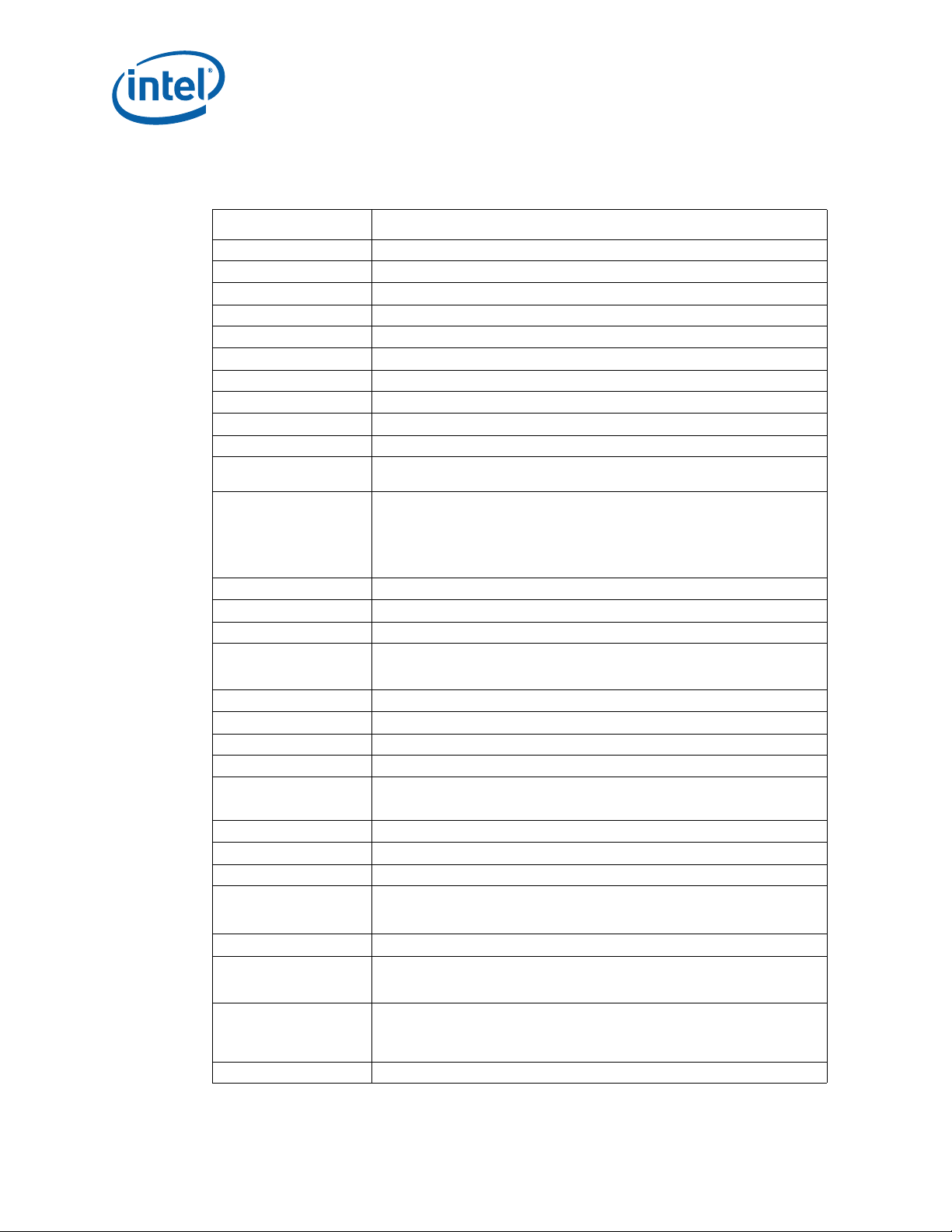
Term Description
BLT Block Level Transfer
CRT Cathode R ay Tube
DDR3 Third generation Double Data Rate SDRAM memory technology
DP DisplayPort*
DMA Direct Memory Access
DMI Direct Media Interface
DTS Digital Thermal Sensor
ECC Error Correction Code
eDP* Embedded DisplayPort*
®
DPST Intel® Disp lay P ower Saving Technology
Intel
Enhanced Intel
SpeedStep
Execute Disa b le Bit
EU Execution Unit
(G)MCH Legacy component - Graphics Memory Controller Hub.
GPU Graphics Processing Unit
ICH
IMC I ntegrated Me mo ry Con troller
Intel
Intel
Intel® TXT Intel® Trusted Execution Technology
Intel
Technology
ITPM Integrated Trusted Platform Module
IOV I/O Virtualization
LCD Liquid Crystal Display
LVDS
MCP Multi- Chip Package
NCTF
PCH
PECI Platform Environment Control Interface
®
Technolog y
®
64 Technology 64-bit memory extensions to the IA-32 architecture.
®
FDI Intel® Flexible Display Interface.
®
Virtualization
Introduction and Features Summary
Technology that provides power management capabilities to laptops.
The Execute Disable bit allows memory to be marked as executable or nonexecutable, when combined with a supporting operating system. If code
attempts to run in non-executable memory the processor raises an error to the
operating system. This feature can prevent some classes of viruses or worms
that exploit buffer overrun vulnerabilities and can thus help improve the overall
security of the system. See the Intel® 64 and IA-32 Architectures Software
Devel oper's Man uals for more detailed information.
The legacy I/O Controller Hub component that contains the main PCI interface,
LPC interface, USB2, Serial ATA, and other I/O functions. It communicates with
the legacy (G)MCH over a proprietary interconnect called DMI.
Processor virtualizatio n which when used in conj unction with Virtual Machine
Monitor software enables multiple, robust independent software environments
inside a single platform.
Low Voltage Differential Signaling
A high speed, low power data transmission standard used for display connections
to LCD panels.
Non-Critical to Function: NCTF locations are typically redundant ground or noncritical reserved, so the loss of the solder joint continuity at end of life conditions
will not affect the overall product functionality.
Platform Controller Hub. The new 2009 chipset with centralized platform
capabilities including the main I/O interfaces along with display connectivity,
audio features, power management, manageability, security and storage
features. The PCH may also be referred to using the code name Ibex Peak.
®
Intel
Datashe et A dd en d um April 2010
TM
Core
i7-620LE/UE, i7-610E, i5-520E and Intel® Celeron® Processor P4500, P4505 Series
12 Document Numbe r: 32 31 78-002
Page 13
Introduc tion and Features Summary
Term Description
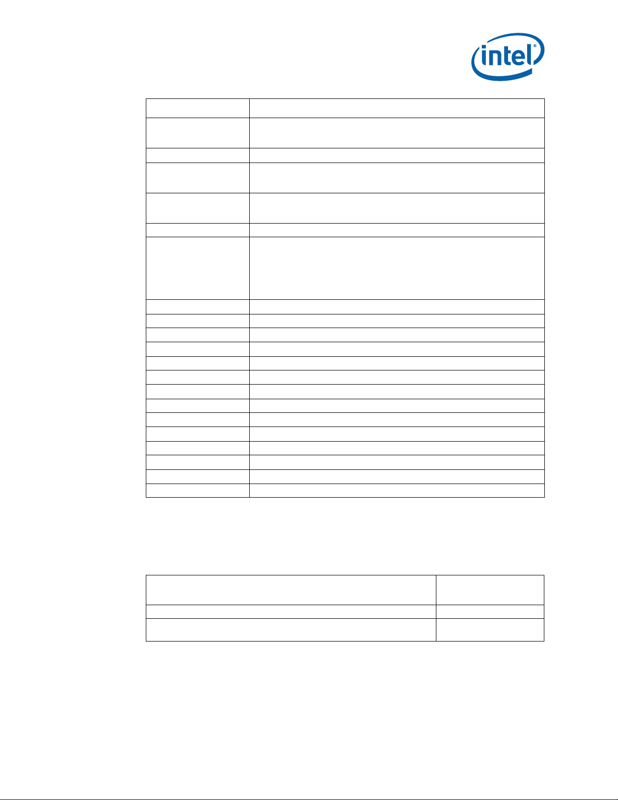
PEG
Processor The 64-bit, single-core or multi-core component (package)
Processo r Co re
Rank
SCI Sy st em Control I nterrupt. Used in ACPI protocol.
Storage Conditions
TA C Thermal Averaging Constant
TDP Thermal Design Power
TOM Top of Mem o r y
TTM Time-To-Market
V
CC
V
SS
V
AXG
V
TT
V
DDQ
VLD Variable Length Decoding
x1 Refers to a Link or Port with one Physical Lane
x4 Refers to a Link or Port with four Physical Lanes
x8 Refers to a Link or Port with eight Physical Lanes
x16 Refers to a Link or Port with sixteen Physical Lanes
PCI Express* Graphics. External Graphics using PCI Express Architecture. A
high-speed serial interface whose configuration is software compatible with the
existing PCI specifications.
The term “processor core” refers to Si die itself which can contain multiple
execution cores. Each execution core has an instruction cache, data cache, and
256-KB L2 cache. All execution cores share the L3 cache.
A unit of DRAM corresponding four to eight devices in parallel, ignoring ECC.
These devices are usually, but not always, mounted on a single side of a SODIMM.
A non-operational state. The processor may be installed in a platform, in a tray,
or loose. Processors may be sealed in packaging or exposed to free air. Under
these conditions, processor landings should not be connected to any supply
voltages, have any I/Os biased or receive any clocks. Upon exposure to “free air”
(i.e., unsealed packaging or a device removed from packaging material) the
processor must be handled in accordance with moisture sensitivity labeling
(MSL) as indicated on the packaging material.
Processor core power supply
Processor ground
Graphics core power supply
L3 shared cache, memory controller, and processor I/O power rail
DDR3 powe r rail
1.5 Related Documents
Refer to the documents in Table 1 for additional information.
Table 1. Processor Documents
Document
Intel® CoreTM i7-600, i5-500 and i3-300 Mobile Processor Series Datasheet http://www.intel.com
Intel® CoreTM i7-620LE/UE, i7-610E and i5-520E Processor Series Datasheet
Addendum Specification Update
April 2010 Datasheet Addendum
Document Number: 32 31 78 - 00 2 13
Intel® Core
TM
i7-620LE/UE, i7-610E, i5-520E and Intel® Celeron® Processor P4500, P4505 Series
Document Number/
Location
http://www.intel.com
Page 14

Table 2. PCH Docu ments
Introduction and Features Summary
Intel® 5 Series Chipset and Intel® 3400 Series Chipset Datasheet http://www.intel.com
Table 3. Public Specifications
Advanced Configuration and Power Interface Specification 3.0 http://www.acpi.info/
PCI Local Bus Specification 3.0
PCI Express Base Specification 2.0 http://www.pcisig.com
DDR3 SDRAM Specification http://www.jedec.org
DisplayPort Specification http://www.vesa.org
®
Intel
64 and IA-32 Architectures Software Developer's Manuals
Volume 1: Basic Architecture 253665
Volume 2A: Instruction Set Reference, A-M 253666
Volume 2B: Instruction Set Reference, N-Z 253667
Volume 3A: System Programming Guide 253668
Volume 3B: System Programming Guide 253669
Document
Document
Document Number/
Location
Document Number/
Location
http://www.pcisig.com/
specifications
http://www.intel.com/
products/processor/
manuals/index.htm
§ §
®
Intel
Datashe et A dd en d um April 2010
14 Document Numbe r: 32 31 78-002
TM
Core
i7-620LE/UE, i7-610E, i5-520E and Intel® Celeron® Processor P4500, P4505 Series
Page 15
Interfaces
2Interfaces
This chapter describes the interfaces supported by the processor.
2.1 System Memory Interface
2.1.1 System Memory Technology Supported
The Integrated Memory Controller (IMC) supports DDR3 protocols with two,
independent, 64-bit wide channels each accessing one DIMM. It supports:
— ECC and non-ECC un-buffered DIMMs. No support for mixed ECC and non-ECC
DIMM configurations.
DDR3 Data Transfer Rates:
— 800 MT/s (PC3-6400), and 1066 MT/s (PC3-8500)
• DDR3 DIMM Modules:
— Raw Card A – single rank x8 unbuffered non-ECC
— Raw Card B – dual rank x8 unbuffered non-ECC
— Raw Card C – single rank x16 unbuffered non-ECC
— Raw Card D – single rank x8 unbuffered ECC
— Raw Card E – dual rank x8 unbuffered ECC
— Raw Card F - dual rank x16 unbuffered non-ECC
• DDR3 DRAM Device Technology:
— Standard 1-Gb, and 2-Gb technologies and addressing are supported for x16
and x8 devices. There is no support for memory modules with different
technologies or capacities on opposite sides of the same memory module. If
one side of a memory module is populated, the other side is either identical or
empty.
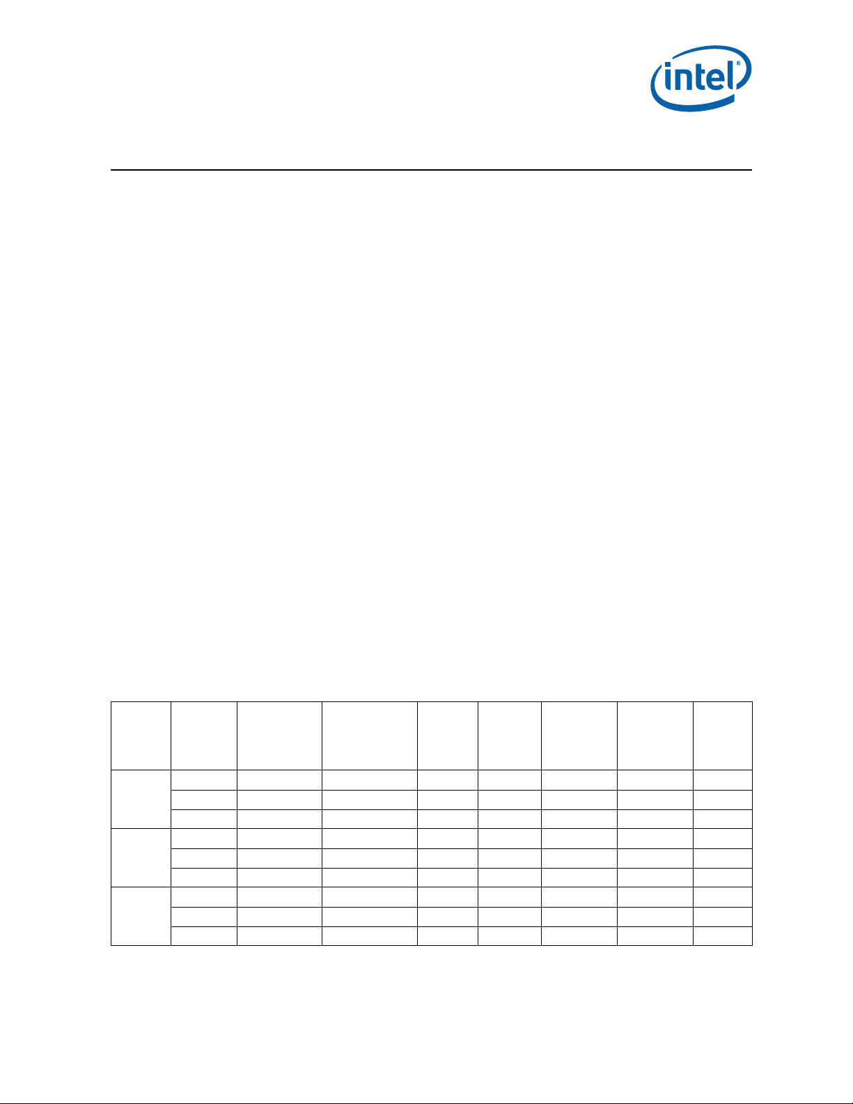
Table 4. Supported DIMM Module Configurations (Sheet 1 of 2)
Raw
Card
Version
A
B
C
April 2010 Datasheet Addendum
Document Number: 32 31 78 - 00 2 15
DIMM
Capacity
512 MB 512 Mb 64 M x 8 8 1 13/10 8 8K
1 GB 1 Gb 128 M x 8 8 1 14/10 8 8K
2 GB 2 Gb 256M x 8 8 1 15/ 10 8 8K
1 GB 512 Mb 64 M x 8 16 2 13/10 8 8K
2 GB 1 Gb 128 M x 8 16 2 14/1 0 8 8K
4 GB 2 Gb 256 M x 8 16 2 15/1 0 8 8K
256MB 512 Mb 32 M x 16 4 1 12/10 8 8K
512 MB 1 Gb 6 4 M x 8 4 1 13 / 10 8 8K
1 GB 2 Gb 128 M x 16 4 1 14/10 8 8K
DRAM
Device
Technology
Intel® Core
DRAM
Organization
TM
i7-620LE/UE, i7-610E, i5-520E and Intel® Celeron® Processor P4500, P4505 Series
# of
DRAM
Devices
# of
Physical
Device
Ranks
# of Row/
Col
Address
Bits
# of
Banks
Inside
DRAM
Page
Size
Page 16
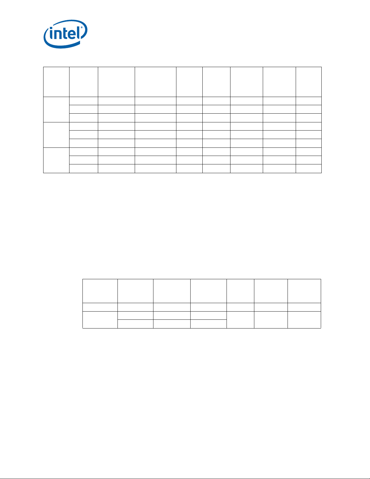
Table 4. Supported DIM M Modu l e Conf igurations (Sheet 2 of 2)
Interfaces
Raw
Card
Version
D
E
F
DIMM
Capacity
512 MB 512 Mb 64 M x 8 9 1 13/10 8 8K
1 GB 1 Gb 128 M x 8 9 1 14/10 8 8K
2 GB 2 Gb 256 M x 8 9 1 15/10 8 8K
1 GB 512 Mb 64M x 8 18 2 13/10 8 8K
2 GB 1 Gb 128 M x 8 18 2 14/10 8 8K
4 GB 2 Gb 256 M x 8 18 2 15/10 8 8K
512 MB 512 Mb 32 M x 16 8 2 12/10 8 8K
1 GB 1 Gb 64 M x 16 8 2 13/10 8 8K
2 GB 2 Gb 128 M x 16 8 2 14/10 8 8K
DRAM
Device
Technology
DRAM
Organization
# of
DRAM
Devices
Physical
Device
2.1.2 System Memory Timing Support
The IMC supports the following DDR3 Speed Bin, CAS Write Latency (CWL), and
command signal mode timings on the main memory interface:
• tCL = CAS Latency
• tRCD = Activate Command to READ or WRITE Command delay
• tRP = PRECHARGE Command Period
•CWL = CAS Write Latency
• Command Signal modes = 1n indicates a new command may be issued every clock
and 2n indicates a new command may be issued every 2 clocks. Command launch
mode programming depends on the transfer rate and memory configuration.
# of
Ranks
# of Row/
Col
Address
Bits
# of
Banks
Inside
DRAM
Page
Size
Table 5. DDR3 System Memory Timing Support
Transfer
Rate
(MT/s)
800 6 6 6 5 1n and 2n 1
1066
NOTES:
1. System Memory timing support is based on availability and is subject to change.
tCL
(tCK)
777
888
tRCD
(tCK)
tRP
(tCK)
CWL
(tCK)
CMD Mode Notes
61n and 2n 1
2.1.3 System Memory Organizati on Modes
The IMC supports two memory organization modes, single-channel and dual-channel.
Depending upon how the DIMM Modules are populated in each memory channel, a
number of different configurations can exist.
2.1.3.1 Single-Channel Mode
In this mode, all memory cycles are directed to a single-channel. Single-channel mode
is used when either Channel A or Channel B DIMM connectors are populated in any
order, but not both.
®
Intel
Datashe et A dd en d um April 2010
16 Document Numbe r: 32 31 78-002
TM
Core
i7-620LE/UE, i7-610E, i5-520E and Intel® Celeron® Processor P4500, P4505 Series
Page 17
Interfaces
2.1.3.2 Dual-Channel Mode - Intel® Flex Memory Technology Mode
The IMC supports Intel® Flex Memory Technology Mode. This mode combines the
advantages of the Dual-Channel Symmetric (Interleaved) and Dual-Channel
Asymmetric Modes. Memory is divided into a symmetric and a asymmetric zone. The
symmetric zone starts at the lowest address in each channel and is contiguous until the
asymmetric zone begins or until the top address of the channel with the smaller
capacity is reached. In this mode, the system runs with one zone of dual-channel mode
and one zone of single-channel mode, simultaneously, across the whole memory array.
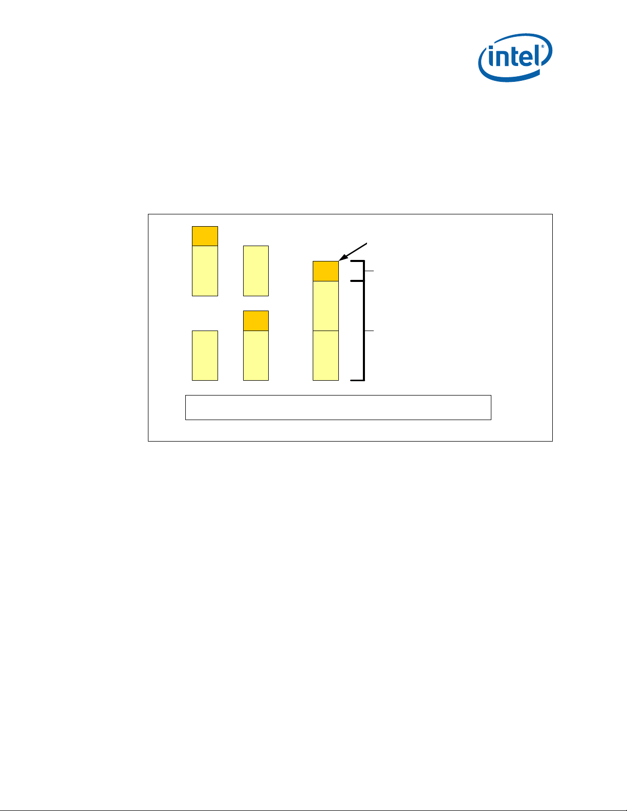
Figure 2. Intel
®
Flex Memory Technology Operation
C
B B
CH BCH A
C
BB
CH BCH A
B – Th e largest physical memory amou nt of the smaller size mem ory m o dule
C – T he rem aining physical mem ory am ount of the la rger siz e m emory mo dule
2.1.3.2.1 Dual-Channel Symmetric Mode
Dual-Channel Symmetric mode, also known as interleaved mode, provides maximum
performance on real world applications. Addresses are ping-ponged between the
channels after each cache line (64-byte boundary). If there are two requests, and the
second request is to an address on the opposite channel from the first, that request can
be sent before data from the first request has returned. If two consecutive cache lines
are requested, both may be retrieved simultaneously, since they are ensured to be on
opposite channels. Use Dual-Channel Symmetric mode when both Channel A and
Channel B DIMM connectors are populated in any order, with the total amount of
memory in each channel being the same.
TOM
C
B
B
Non interleaved
access
Du al channel
interleaved access
When both channels are populated with the same memory capacity and the boundary
between the dual channel zone and the single channel zone is the top of memory, IMC
operates completely in Dual-Channel Symmetric mode.
Note: The DRAM device technology and width may vary from one channel to the other.
2.1.3.2.2 Dual-Channel Asymmetric Mode
This mode trades performance for system design flexibility. Unlike the previous mode,
addresses start at the bottom of Channel B and stay there until the end of the highest
rank in Channel B, and then addresses continue from the bottom of Channel A to the
top. Real world applications are unlikely to make requests that alternate between
addresses that sit on opposite channels with this memory organization, so in most
cases, bandwidth is limited to a single channel.
April 2010 Datasheet Addendum
Document Number: 32 31 78 - 00 2 17
Intel® Core
TM
i7-620LE/UE, i7-610E, i5-520E and Intel® Celeron® Processor P4500, P4505 Series
Page 18

Interfaces
This mode is u sed whe n Inte l® Flex Memory Technology is disabled and both Channel A
and Channel B DIMM connectors are populated in any order with the total amount of
memory in each channel being different.
Figure 3. Dual-Channel Symmetric (Interleaved) and Dual-Channel Asymmetric Modes
Dual Channel Interleaved
(memory sizes mus t m atch)
CL
CH. B
CH. A
CH. B
CH. A
CH. B
CH. A
Top of
Memory
0
Dual Channel Asymmetric
(memory sizes can differ)
2.1.4 Rules for Populating Memory Slots
CL
CH. A
CH. B
Top of
Memory
CH.B-top
DRB
0
In all modes, the frequency of system memory is the lowest frequency of all memory
modules placed in the system, as determined through the SPD registers on the
memory modules. The system memory controller supports only one DIMM connector
per channel.For dual-channel modes both channels must have an DIMM connector
populated and for single-channel mode only a single-channel must have an DIMM
connector populated.
2.1.5 Technology Enhancements of Intel® Fast Memory Access (Intel® FMA)
The following sections describe the Just-in-Time Scheduling, Command Overlap, and
Out-of-Order Scheduling Intel
2.1.5.1 Just-in-Time Command Scheduling
The memory controller has an advanced command scheduler where all pending
requests are examined simultaneously to determine the most efficient request to be
issued next. The most efficient request is picked from all pending requests and issued
to system memory Just-in-Time to make optimal use of Command Overlapping. Thus,
instead of having all memory access requests go individually through an arbitration
mechanism forcing requests to be executed one at a time, they can be started without
®
Intel
Datashe et A dd en d um April 2010
18 Document Numbe r: 32 31 78-002
TM
Core
i7-620LE/UE, i7-610E, i5-520E and Intel® Celeron® Processor P4500, P4505 Series
®
FMA technology enhancements.
Page 19

Interfaces
interfering with the current request allowing for concurrent issuing of requests. This
allows for optimized bandwidth and reduced latency while maintaining appropriate
command spacing to meet system memory protocol.
2.1.5.2 Command Overlap
Command Overlap allows the insertion of the DRAM commands between the Activate,
Precharge, and Read/Write commands normally used, as long as the inserted
commands do not affect the currently executing command. Multiple commands can be
issued in an overlapping manner, increasing the efficiency of system memory protocol.
2.1.5.3 Out-of-Order Scheduling
While leveraging the Just-in-Time Scheduling and Command Overlap enhancements,
the IMC continuo usl y monit or s pen ding req uest s to sy st em memory f or the best use of
bandwidth and reduction of latency. If there are multiple requests to the same open
page, these requests would be launched in a back to back manner to make optimum
use of the open memory page. This ability to reorder requests on the fly allows the IMC
to further reduce latency and increase bandwidth efficiency.
2.1.6 DRAM Clock Generation
T wo differential clock pairs for every supported DIMM. There are total of four clock pairs
driven directly by the processor to two DIMMs.
2.1.7 DDR3 On-Die Termination
On-Die Termination (ODT) is a feature that allows a DRAM device to turn on/off internal
termin ation resi stan ce for ea ch DQ, DQS/DQ S#, and DM sign al via the ODT contr ol pin.
The ODT feature improves signal integrity of the memory channel by allowing the
DRAM controller to independently turn on or off the termination resistance for any or all
DRAM devices themselves instead of on the motherboard.
The IMC drives out the required ODT signals, based on the memory configuration and
which rank is being written to or read from, to the DRAM devices on a targeted DIMM
module rank to enable or disable their termination resistance.
2.2 PCI Express* Interface
This section describes the PCI Express* interface capabilities of the processor. See the
PCI Expres s Bas e Spe ci fica t ion for further details on PCI Express.
The processor has two options for PCI Express controllers available:
• 1 x16 PCI Express Port
or
•2 x8 PCI Express Ports
— Enabled with CFG[0] strapping, see Section 2.2.2 an d Section 3.2
2.2.1 PCI Express* Configuration Mechanism
The PCI Express* link is mapped through a PCI-to-PCI bridge structure.
April 2010 Datasheet Addendum
Document Number: 32 31 78 - 00 2 19
Intel® Core
TM
i7-620LE/UE, i7-610E, i5-520E and Intel® Celeron® Processor P4500, P4505 Series
Page 20

Interfaces
Figure 4. PCI Express* Related Register Structures in the
Intel
®
Core
TM
i7-620LE/UE, i7-610E, i5-520E and Intel® Celeron® Processor
P4500, P4505 Series
PCI Express
Device
PCI Express
Device
Port 0
Port 1
PCI- PCI Bridge
representing r oot
PCI Express port
(Device 1)
PCI- PCI Bridge
representing r oot
PCI Express port
(Device 6)
2.2.2 PCI Express Port Bifurcation
When bifurcated, the wires which had previously been assigned to lanes 15:8 of the
single x16 primary port (Port 0) are reassigned to lanes 7:0 of the x8 secondary port
(Port 1). This assignment applies whether the lane numbering is reversed or not. The
controls for the secondary port (Port 1) and the associated virtual PCI-to-PCI bridge
can be found in PCI Device 6.
PCI Compatible
Host Bridge Device
(Device 0)
DMI
When the primary port is not bifurcated, Device 6 is hidden from the discovery
mechanism used in PCI enumeration, such that configuration of the device is neither
possible nor necessary.
®
Intel
Datashe et A dd en d um April 2010
20 Document Numbe r: 32 31 78-002
TM
Core
i7-620LE/UE, i7-610E, i5-520E and Intel® Celeron® Processor P4500, P4505 Series
Page 21
Signal Description
3 Signal Description
This chapter describes the processor signals. They are arranged in functional groups
according to their associated interface or category. The following notations are used to
describe the signal type:
Notatio n s Signal Ty pe
IInput Pin
OOutput Pin
I/O Bi-directional Input/Output Pin
The signal description also includes the type of buffer used for the particular signal:
Table 6. Signal Description Buffer Types
Signal Description
PCI Express*
FDI
DMI
CMOS CMOS buffers. 1.1-V tolerant
DDR3 DDR3 buffers: 1.5-V tolerant
A
GTL Gunning Transceiver Logic signaling technology.
Ref Voltage reference signal.
Asynchronous
1
PCI Express interface signals. These signals are compatible with PCI Express 2.0
Signalling Environment AC Specifications and are AC coupled. The buffers are not 3.3V tolerant. Refer to the PCIe specification.
Intel Flexible Display interface signals. These signals are compatible with PCI Express
2.0 Signaling Environment AC Specifications, but are DC coupled. The buffers are not
3.3-V tolerant.
Direct Media Interface signals. These signals are compatible with PCI Express 2.0
Signaling Environment AC Specifications, but are DC coupled. The buffers are not 3.3V tole rant.
Analog reference or output. May be u sed as a threshold voltage or for buffer
compensation.
Signal has no timing relationship with any reference clock.
NOTES:
1. Qualifier for a buffer type.
3.1 System Memory Interface
Table 7. Memory Channel A (Sheet 1 of 2)
Signal Name Description
SA_BS[2:0]
SA_WE#
April 2010 Datasheet Addendum
Document Number: 32 31 78 - 00 2 21
Intel® Core
TM
Bank Select: These signals define which banks
are se lected within each SD RAM rank.
Write Enable Control Signal: Used with
SA_RAS# and SA_CAS# (along with SA_CS#) to
define the SDRAM Commands.
i7-620LE/UE, i7-610E, i5-520E and Intel® Celeron® Processor P4500, P4505 Series
Direction/Buffer
Type
O
DDR3
O
DDR3
Page 22

Table 7. Memory Channel A (Sheet 2 of 2)
Signal Description
Signal Name Description
SA_RAS#
SA_CAS#
SA_DM[7:0]
SA_DQS[8]
SA_DQS[7:0]
SA_DQS#[8]
SA_DQS#[7:0]
SA_DQ[71:64]
SA_DQ[63:0]
SA_MA[15:0]
SA_CK[1:0]
SA_CK#[1:0]
SA_CKE[1:0]
SA_CS#[1:0]
SA_ODT[1:0] O n Die Termination: Active Termination Control.
RAS Control Signal: Used with SA_CAS# and
SA_WE# (along with SA_CS#) to define the SRAM
Commands.
CAS Control Signal: Used with SA_RAS# and
SA_WE# (along with SA_CS#) to define the SRAM
Commands.
Data Mask: These signals ar e used to mask
individual bytes of data in the case of a partial
write and to interrupt burst writes. When activated
during writes, the corresponding data groups in
the SDRAM are masked. There is one SA_DM[7:0]
for every data byte lane.
ECC Data Strobe: SA_DQS[8] is the data strobe
for the ECC check data bits SA_DQ[71:64]
Note: Not required for non-ECC mode
Data Strobes: SA_DQS[7:0] and its complement
signal group make up a differential strobe pair . The
data is captured at the crossing point of
SA_DQS[7:0] and its SA_DQS#[7:0] during read
and write transactions
ECC Data Strobe Complement: SA_DQS#[8] is
the complement strobe for the ECC check data bits
SA_DQ[71:64]
Note: Not required for non-ECC mode
Data Strobe Complements: These are the
complementary str obe signals .
ECC Check Data Bits: SA_DQ[71:64] are the ECC
check data bits for Channel A.
Note: Not required for non-ECC mode
Data Bus: Channel A data signal interface to the
SDRAM data bus.
Memory Address: These signals are used to
provide the multiplexed row and column address
to the SDRAM.
SDRAM Differential Clock: Channel A SDRAM
Differential clock signal pair. The crossing of the
positive edge of SA_CK and the negative edge of
its complement SA_CK# are used to sample the
command and control signals on the SDRAM.
SDRAM Inverted Differential Clock: Channel A
SDRAM Differential clock signal-pair complement.
Clock Enable: (1 per rank) Used to:
- Initialize the SDRAMs during power-up
- Power-down SD RAM ranks
- Place all SDRAM ranks into a nd out of se lf-refresh
during STR
Chip Select: (1 per rank) Used to select particular
SDRAM components during the active state. There
is one Chip Select for each SDRAM rank.
Direction/Buffer
Type
O
DDR3
O
DDR3
O
DDR3
I/O
DDR3
I/O
DDR3
I/O
DDR3
I/O
DDR3
I/O
DDR3
I/O
DDR3
O
DDR3
O
DDR3
O
DDR3
O
DDR3
O
DDR3
O
DDR3
®
Intel
Datashe et A dd en d um April 2010
22 Document Numbe r: 32 31 78-002
TM
Core
i7-620LE/UE, i7-610E, i5-520E and Intel® Celeron® Processor P4500, P4505 Series
Page 23

Signal Description
Table 8. Memory Channel B (Sheet 1 of 2)
Signal N ame Descr iption
SB_BS[2:0]
SB_WE#
SB_RAS#
SB_CAS#
SB_DM[7:0]
SB_DQS[8]
SB_DQS[7:0]
SB_DQS#[8]
SB_DQS#[7:0]
SB_DQ[71:64]
SB_DQ[63:0]
SB_MA[15:0]
SB_CK[1:0]
SB_CK#[1:0]
SB_CKE[1:0]
SB_CS#[1:0]
Bank Select: These signals define which banks
are se lected withi n each SDRAM rank.
Write Enable Control Signal: Used with
SB_RAS# and SB_CAS# (along with SB_CS#) to
define the SDRAM Commands.
RAS Control Signal: Used with SB_CAS# and
SB_WE# (along with SB_CS#) to define the SRAM
Commands.
CAS Control Signal: Used with SB_RAS# and
SB_WE# (along with SB_CS#) to define the SRAM
Commands.
Data Mask: These signals are used to mask
individual bytes of data in the case of a partial
write, and to interrupt burst writes. When
activa ted during writes, the corr esponding d at a
groups in the SDRAM are masked. There is one
SB_DM[7:0] for every data byte lane.
ECC Data Strobe: SB_DQS[8] is the data strobe
for the ECC check data bits SB_DQ[71:64]
Note: Not required for non-ECC mode
Data Strobes: SB_DQS[7:0] and its complement
signal group make up a differential strobe pair. The
data is captured at the crossing point of
SB_DQS[7:0] and its SB_DQS#[7:0] during read
and write transactions.
ECC Data Strobe Complement: SB_DQS#[8] is
the complement strobe for the ECC check data bits
SB_DQ[71:64]
Note: Not required for non-ECC mode
Data Strobe Complements: These are th e
complementary strobe signals.
ECC Check Data Bits: SB_DQ[71: 64] are the ECC
check data bits for Channel B
Note: Not required for non-ECC mode
Data Bus: Channel B data signal interface to the
SDRAM data bus.
Memory Address: These signals are used to
provide the multiplexed row and column address
to the SDRAM.
SDRAM Differential Clock: Channel B SDRAM
Differential clock signal pair. The crossing of the
positive edge of SB_CK and the negative edge of
its complement SB_CK# are used to sample the
command and control signals on the SDRAM.
SDRAM Inverted Differential Clock: Channel B
SDRAM Differential clock signal-pair complement.
Clock Enable: (1 per rank) Used to:
- Initialize the SDRAMs during power-up.
- Power-down SDRAM ranks.
- Place all SDRAM ranks into and out of self -refresh
during STR.
Chip Select: (1 per rank) Used to select particular
SDRAM components during the active state. There
is one Chip Select for each SDRAM rank.
Direction/Buffer
Type
O
DDR3
O
DDR3
O
DDR3
O
DDR3
O
DDR3
I/O
DDR3
I/O
DDR3
I/O
DDR3
I/O
DDR3
I/O
DDR3
I/O
DDR3
O
DDR3
O
DDR3
O
DDR3
O
DDR3
O
DDR3
April 2010 Datasheet Addendum
Document Number: 32 31 78 - 00 2 23
Intel® Core
TM
i7-620LE/UE, i7-610E, i5-520E and Intel® Celeron® Processor P4500, P4505 Series
Page 24

Table 8. Memory Channel B (Sheet 2 of 2)
Signal Description
Signal Name Description
SB_ODT[1:0] On Die Termination: Active T erm ination Control.
3.2 Reset and Miscellaneous Signals
Table 9. Reset and Misce l laneous Signals
Signal N ame Desc ription
SM_DRAMRST#
CFG[17:0]
DDR3 DRAM Reset: Reset signal from processor
to DRAM devices. One for all channels of DIMMs.
Configuration signals:
The CFG signals have a default value of 1 if not
terminated on the board. Refer to the Platfo rm
Design Guide for pull-down recommendations
when logic low is desired.
• CFG[0]: PCI Express* Bifurcation:
—1 = 1 x16 PCI Express I/O
— 0 = 2 x 8 PCI Express I/O
• CFG[1]: Rese rve d
• CFG[2]: Reserved configuration lands. A test
point may be placed on the board for this land.
• CFG[3]: PCI Express* Static Lane Numbering
Reversal. A test point may be placed on the
board for this land. Lane reversal will be
applied across all 16 lanes.
—1: No Reversal
—0: Reversal
In the case of Bifurcation with NO Lane Reversal
the physical lane mapping is as follows:
— Lanes 15:8 => Port 1 Lanes 7:0
— Lanes 7: 0 => Po rt 0 Lanes 7:0
In the case of Bifurcation with WITH Lane Reversal
the physical lane mapping is as follows:
— Lanes 15:8 => Port 0 Lanes 0:7
— Lanes 7: 0 => Po rt 1 Lanes 0:7
• CFG[4]: Embedded DisplayPort Detection:
This is used to detect the presence of a device
on the Embedded DisplayPort.
— 1: No Physical Display Port attached to
the Embedded Display Port
— 0: An external Display Port device is
connected to the Embedded Display Port
• CFG[17:5]: Reserved configuration lands.
Intel does not recommend a test point on the
board for these lands.
Direction/Buffer
Type
O
DDR3
Direction/Buffer
Type
O
DDR3
I
CMOS
§ §
®
Intel
Datashe et A dd en d um April 2010
24 Document Numbe r: 32 31 78-002
TM
Core
i7-620LE/UE, i7-610E, i5-520E and Intel® Celeron® Processor P4500, P4505 Series
Page 25
Electrical Specifications
4 Electrical Specifications
4.1 Signal Groups
Signals are grouped by buffer type and similar characteristics as listed in Table 10. The
buffer type indicates which signaling technology and specifications apply to the signals.
All the differential signals, and selected DDR3 and Control Sideband signals have OnDie Termination (ODT) resistors. There are some signals that do not have ODT and
need to be terminated on the board.
Table 10. Mobile Signal Groups
Signal Group
DDR3 Data Signals
Single ended (e) DDR3 Bi-directional SA_DQ[71:0], SB_DQ[71:0]
Differential (f) DDR3 Bi-directional
Power/Ground/Other
Single Ended (z) Other DBR#, PROC_DETECT, VCAP0, VCAP1, VCAP2
1
Alpha
Group
2
NOTES:
1. Refer to Chapter 3 for signal description details.
2. SA and SB refer to DDR3 Channel A and DDR3 Channel B.
All Control Sideband Asynchronous signals are required to be asserted/deasserted for
at least eight BCLKs in order for the processor to recognize the proper signal state. See
Section 4.2 for the DC specif icat io ns.
4.2 DC Specifications
The processor DC specifications in this section are defined at the processor
pins, unless noted otherwise. See Chapter 5 for the processor pin listings and
Chapter 3 for signal definitions.
The DC specifications for the DDR3 signals are listed in Table 11.
Type Signals
SA_DQS[8:0], SA_DQS#[8:0]
SB_DQS[8:0], SB_DQS#[8:0]
4.2.1 Voltage and Current Specifications
Table 11. DDR3 Signal Group DC Specifications (Sheet 1 of 2)
Symbol Parameter
V
IL
Input L o w Voltage (e,f) 0.43*V
Alpha
Group
Min Typ Max Units Notes
DDQ
V2,4
NOTES:
1. Unless otherwise noted, all specifications in this table apply to all processor frequencies.
2. V
3. V
4. V
5. R
April 2010 Datasheet Addendum
Document Number: 32 31 78 - 00 2 25
is defined as the maximum voltage level at a receiving agent that will be interpreted as a logical low value.
IL
is defined as the minimum voltage level at a receiving agent that will be interpreted as a logical high value.
IH
and VOH may experience exc u rsio ns abo ve V
IH
specifications.
is the termination on the DIMM and in not controlled by the processor.
VTT_TERM
Intel® Core
TM
i7-620LE/UE, i7-610E, i5-520E and Intel® Celeron® Processor P4500, P4505 Series
. However, input signal drivers must comply with the signal quality
DDQ
1,9
Page 26
Table 11. DDR3 Signal Group DC Specifications (Sheet 2 of 2)
Electrical Specifications
Symbol Parameter
V
IH
V
OL
V
OH
Input Hi gh Voltage (e, f) 0.57*V
Output Low Volt age (c,d,e,f)
Output High Voltage (c,d,e,f)
Alpha
Group
Min Typ Max Units Notes
DDQ
/ 2)* (R
(V
DDQ
(R
ON+RVTT_TERM
- ((V
V
DDQ
(R
(R
ON+RVTT_TERM
ON
DDQ
/
/
ON
))
/ 2)*
))
NOTES:
1. Unless otherwise noted, all specifications in this table apply to all processor frequencies.
2. V
3. V
4. V
5. R
is defined as the maximum voltage level at a receiving agent that will be interpreted as a logical low value.
IL
is defined as the minimum voltage level at a receiving agent that will be interpreted as a logical high value.
IH
and VOH may experience exc ursions abo ve V
IH
specifications.
is the termination on the DIMM and in not controlled by the processor.
VTT_TERM
. However, input signal drivers must comply with the signal quality
DDQ
1,9
V3
5
V4,5
®
Intel
Datashe et A dd en d um April 2010
TM
Core
i7-620LE/UE, i7-610E, i5-520E and Intel® Celeron® Processor P4500, P4505 Series
26 Document Numbe r: 32 31 78-002
Page 27

Process or Ball and Signal Information
5 Processor Ball and Signal
Information
5.1 Processor Ball Assignments
• Table 12 provides a listing of all processor pins ordered alphabetically by ball name
for the Intel
P4500, P4505 Series package respectively.
• Table 13 provides a listing of all processor pins ordered alphabetically by ball
number for the Intel® Core
Processor P4500, P4505 Series package respectively.
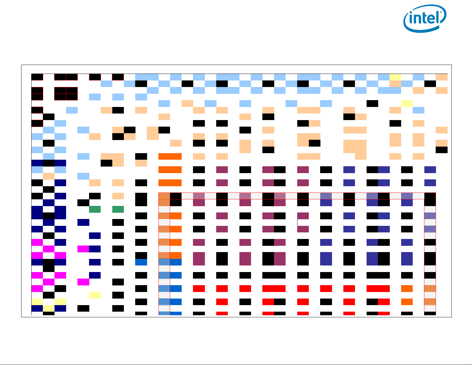
• Figure 5, Figure 6, Figure 7, and Figure 8 show the Top-Down view of the Intel
TM
Core
P4505 Series ballmap
®
TM
Core
i7-620LE/UE, i7-610E, i5-520E and Intel® Celeron® Processor P4500,
i7-620LE/UE, i7-610E , i5-52 0E and Int el® Celeron® Process or
TM
i7-620LE/UE, i7-610E, i5-520E and Intel® Celeron®
®
April 2010 Datasheet Addendum
Document Number: 32 31 78 - 00 2 27
Intel® Core
TM
i7-620LE/UE, i7-610E, i5-520E and Intel® Celeron® Processor P4500, P4505 Series
Page 28
Processor Ball and Signal Information
Figure 5. Intel® Core
TM
i7-620LE/UE, i7-610E, i5-520E and Intel® Celeron® Processor P4500, P4505 Series Ballmap
(Top View, U pper-Left Quadrant)
71 70 69 68 67 66 65 64 63 62 61 60 59 58 57 56 55 54 53 52 51 50 49 48 47 46 45 44 43 42 41 40 39 38 37 36
DC_TES
BV
T_BV71
BU
DC_TES
BT
T_BT71
DC_TES
BR
T_BR71
BP
VSS
BN
BM
VSS
BL
BK
SB_DQ[5
BJ
6]
BH
SB_DQ[5
BG
8]
BF
RSVD VSS RSVD VSS
BE
SB_DQ[6
BD
2]
BC
VSS RSVD
BB
BA
VSS RSVD VSS
AY
AW
RSVD RSVD
AV
RSVD VSS RSVD VSS VT T0 VT T0 VSS VCAP0 VSS VC AP0 VSS VC AP0 VSS VCAP1 VSS VCAP1 VSS VCAP 1
AU
AT
RSVD RSVD VS S VTT 0 VTT 0 VS S VC AP0 VSS VCAP0 VSS VCAP0 VSS VCAP 1 VS S VC AP1 VSS VCAP1
AR
AP
GFX_ VID
AN
[4]
AM
GFX_DP
AL
RSLPVR
RSVD VSS RSVD RSVD VSS VCAP 2 VCAP2 VCAP2 VCAP0 VS S VC AP0 VSS VCAP0 VSS VCAP1 VSS VC AP1 VSS VC AP1 VSS
AK
AJ
GFX_ VID
AH
[3]
AG
GFX_ VID
AF
[0]
AE
COMP3 COMP1 VSS VCAP2 VCAP2 VSS VCC VSS VCC VSS VC C VSS VCC VSS VCC VT T0 VT T0
AD
RSVD COMP2 RSVD VSS VSS
AC
DC_TES
DC_TES
T_BV69
T_BV68
DC_TES
VSS
T_BT69
VSS VSS
SB_DQ[5
VSS
SB_DQ[6
0]
VSS
SB_DQ[5
7]
SA_DQ[6
3]
VSS
RSVD VSS VS S VT T0 VSS VCAP 0 VS S VC AP0 VSS VCAP0 VSS VCAP1 VSS VC AP1 VSS VC AP1 VSS
RSVD RSVD VSS
VSS RSVD VSS
GFX_ VID
[6]
VSS
GFX_ VID
[2]
VSS COMP0 VSS
4]
SB_DQ[5
5]
SB_DQS
[7]
SB_DQS
#[7]
SB_DQ[6
3]
RSVD VSS VT T0 VT T0 VCAP0 VSS VCAP 0 VS S VC AP0 VSS VCAP1 VSS VCAP 1 VS S VC AP1 VSS
GFX_IM
ON
GFX_ VR
_EN
VSS VSS VCAP2 VCAP2 VCC VCC VCC VC C VCC VC C VCC VC C VCC VCC VTT 0 VTT 0
VSS VSS
SB_DM[6
]
SB_DQ[5
0]
SB_DQ[6
1]
SA_DQ[6
0]
SB_DM[7
]
SB_DQ[5
9]
SA_DQ[5
9]
PM_EXT
_TS#[0]
GFX_ VID
RSVD VSS
[5]
RSVD VSS VCAP2 VCAP2 VSS VSS VS S VS S VS S VS S VS S VS S VS S VSS VS S VS S
GFX_ VID
[1]
SB_DQ[5
1]
SA_DQ[5
VSS
0]
SA_DQ[5
4]
VSS
SA_DQ[61]SA_DQ[5
7]
SA_DQS[
7]
SA_DQ[5
8]
SA_DQ[6
2]
PM_EXT
_TS#[1]
VSS
SB_DQS
SB_DQ[4
[6]
SB_DQS
#[6]
VSS
SA_DQ[5
6]
8]
VSS
SB_DQ[5
3]
SB_DQ[5
2]
SA_DM[6
]
SA_DQ[5
5]
SA_DQ[5
1]
VSS VTT0 VTT0
SA_DQS
#[7]
VSS VT T0 VT T0 VSS VCAP0 VSS VC AP0 VSS VC AP0 VSS VCAP1 VSS VCAP1 VSS VCAP 1
VSS VT T0 VSS VCAP0 VSS VCAP 0 VS S VC AP0 VSS VCAP1 VSS VCAP 1 VS S VC AP1 VSS
VSS VT T0 VT T0 VCAP0 VSS VCAP 0 VS S VC AP0 VSS VCAP1 VSS VCAP 1 VS S VC AP1 VSS
SB_DQ[4
7]
SB_DQ[4
6]
SB_DQ[4
2]
SB_DQ[4
9]
SA_DQS[
6]
VSS VSS
SA_DM[7
VTT 0 VTT 0 VSS VCAP 0 VS S VC AP0 VSS VCAP0 VSS VCAP1 VSS VCAP 1 VS S VC AP1
SB_DM[5
]
VSS
SB_DQ[4
3]
SA_DQS
#[6]
SA_DQ[4
9]
VSS VSS VSS
SA_DQ[5
3]
]
VSS VSS
SA_DQ[5
2]
SB_DQS
[5]
SB_DQ[4
5]
SB_DQS
SB_DQ[3
#[5]
9]
VSS
SB_DQ[44]SB_DQ[3
8]
SA_DQ[4
7]
SA_DQ[4
3]
SA_DQ[4
8]
SB_DQ[4
1]
SB_DQ[4
0]
SA_DQ[4
6]
SA_DQ[4
2]
SA_DM[5
]
SB_DQ[3
7]
SB_DQS
[4]
SB_DQ[3
4]
VSS
SB_DQS
#[4]
SA_DQ[4
1]
VSS VSS
SA_DQS
#[5]
SA_DQS[
5]
VSS
SB_ODT
[1]
SB_DQ[3
5]
SB_DQ[33]SB_DM[4
]
VSS
SB_DQ[32]SB_DQ[3
6]
SA_DQ[40]SA_DQ[3
9]
SA_ODT[
1]
SA_DQ[45]SA_CS#[
1]
SA_DQ[4
VSS
4]
SA_DQ[35]SA_DQ[3
4]
SB_CAS
#
SB_CS#[
0]
SB_ODT
[0]
SB_MA[1
3]
SB_BS[1
]
VSS
SB_CS#[
1]
SA_DQ[3
8]
SA_DQ[3
3]
SA_DQS[4]SA_CAS
#
SA_DQS
SA_DQ[3
#[4]
7]
SA_DM[4]SA_DQ[7
0]
SA_ODT[
0]
SB_MA[1
0]
VSS
SB_BS[0]SM_RCO
MP[2]
SA_DQ[66]SB_CK#[
SB_RAS
SB_WE#
#
SA_DQ[3
6]
VSS
SA_DQ[3
2]
SA_CS#[
0]
SA_MA[1
3]
1]
SM_RCO
MP[1]
SB_CK[1
]
SA_BS[0]
SB_DQ[6
8]
SA_RAS
#
SA_DQ[7
1]
SA_BS[1]
SA_WE#
SA_MA[2
]
VSS
SA_MA[0
]
SA_CK#[
1]
SA_CK[1
]
VSS
323178-002 28
Page 29

Processor Ball and Signal Information
VCCPW
SM_DRA
Figure 6. Intel® Core
TM
i7-620LE/UE, i7-610E, i5-520E and Intel® Celeron® Processor P4500, P4505 Series Ballmap
(Top View, Upper-Right Qu adrant)
3534333231302928272625242322212019181716151413121110987654321
SB_CK#[0]SM_RCO
SA_DQ[6
7]
SA_CK#[
0]
VDDQ
VDDQ VDDQ VDDQ VDDQ VDDQ VDDQ VDDQ VDDQ VDDQ VDDQ VDDQ VDDQ
VSS VSS VSS VSS VSS VS S VS S VS S VSS VSS VS S VSS VSS VSS VT T0 VS S
VTT0 VTT0
VSS VSS VSS VSS VSS VS S VS S VS S VSS VSS VS S VSS VSS VT T0 VSS RSVD
VSS VSS VSS VSS VSS VS S VS S VS S VSS VSS VS S VSS VSS VT T0 VSS VSS
VTT 0 VTT 0 VAXG VAXG VAXG VAXG VAXG VAXG VAXG VAXG VTT 0 VTT 0 VTT 0 VTT 0 VTT 0
VSS VSS VAXG VAXG VAXG VAXG VAXG VAXG VAXG VAXG VTT 0 VTT 0 VTT 0 VTT 0 CFG[0] VSS
VTT 0 VT T0 VS S VS S VSS VS S VS S VSS VS S VS S VSS VS S VAXG VAXG BC LK # BC LK CFG[4] CFG[3] CFG[2]
VSS VSS VSS VSS VSS VS S VS S VS S VSS VSS VS S VSS VAXG VAXG VSS CFG[10]
VTT 0 VTT 0 VTT 0 VTT 0 VAXG VAXG VAXG VAXG VAXG VAXG VAXG VAXG VAXG
VTT 0 VTT 0 VTT 0 VTT 0 VAXG VAXG VAXG VAXG VAXG VAXG VAXG VTT1 VTT1 VTT1 VSS CFG[14]
MP[0]
SB_CK[0
]
SB_MA[0]SB_MA[5
]
SA_MA[1
]
SA_CK[0
]
VSS
SA_MA[1
0]
SA_MA[3
]
SA_DQS[8]SA_DQS
VSS
SA_MA[5
]
VSS
SA_MA[6
]
SB_DQ[6
6]
SA_MA[4
]
#[8]
VTT0_D
DR
SB_MA[4
]
SB_MA[6
]
SB_MA[3
]
SB_MA[1
]
SA_MA[8
]
SB_DQ[7
0]
SA_MA[7
]
SA_MA[1
1]
VSS
SA_DQ[6
4]
VTT0_D
DR
SB_MA[2
]
SB_MA[1
2]
SB_DQ[7
1]
SA_MA[1
4]
VSS
SA_MA[1
2]
SA_DQ[6
9]
SA_MA[9
]
SA_DQ[6
5]
VTT0_D
DR
SB_MA[8]SB_MA[1
4]
SB_MA[1
1]
SB_MA[9]SB_CKE[
0]
SB_MA[7
]
SA_DQ[6
8]
VTT0_D
DR
SB_BS[2
]
VSS
SB_CKE[
1]
SA_MA[15]SA_DM[3
]
SB_DQ[6
VSS VSS
7]
SA_DQ[26]SA_CKE[
1]
SA_DQ[2
VSS
7]
SA_DQ[31]SA_DQ[3
0]
SB_DQ[65]SB_DQ[6
VTT0_DDRVTT0_D
SB_MA[1
5]
9]
DR
SB_DQ[2
6]
SB_DQ[2
7]
SB_DM[3
]
SB_DQ[30]SB_DQ[2
VSS
SB_DQ[31]SB_DQS
SA_DQS[3]SA_DQ[2
4]
SA_DQS
VSS
#[3]
SA_DQ[2
VSS
8]
SA_DQ[2
VSS
9]
SA_CKE[
SA_BS[2]
0]
SB_DQ[6
4]
VTT0_D
DR
9]
SB_DQ[2
5]
#[3]
SB_DQ[2
8]
SB_DQS
[8]
VTT0_D
DR
VSS
SB_DQ[2
2]
SB_DQ[2
3]
SB_DQS
[3]
SA_DQ[1
6]
SA_DQ[2
3]
SA_DQ[1
8]
SA_DQ[1
9]
VDDQ VDDQ VSS
SB_DQS
#[8]
VTT0_D
DR
SB_DQ[1
9]
SB_DQ[1
8]
SB_DQ[2
4]
SA_DM[2
]
SA_DQ[2
2]
VSS
SA_DQ[2
5]
VDDQ VSS
VTT0_D
DR
SB_DQS
[2]
VSS
SB_DM[2]SB_DQ[1
SA_DQS
#[2]
SA_DQS[
2]
SA_DQ[1
1]
VDDQ_C
K
VTT0 VTT0
SB_DQ[2
0]
SB_DQS
#[2]
7]
SB_DQ[2
1]
SM_DRA
MRST#
VDDQ_C
K
VAXG_S
ENSE
SB_DQ[1
5]
VSS
SB_DQ[1
6]
SA_DQ[2
0]
VSS
SA_DQ[1
0]
SA_DQ[9
]
SA_DQ[8
]
SA_DM[0]SA_DQ[3
VSS
VTT0 VSS
VAXG CFG[5]
VSSAXG
_SENSE
RSVD_N
CTF
SB_DQ[1
4]
SB_DQ[1
1]
SA_DQ[17]SA_DQ[1
5]
SA_DQ[2
1]
VSS
SA_DQ[1
VSS
2]
SA_DQ[7
VSS
]
]
VSS
SA_DQ[0
]
VSS CFG[7] VSS CFG[9]
CFG[15] CFG[16] CFG[8] VSS
FDI_FSY FDI_FSY
RSVD_N
CTF
VSS
SB_DQ[10]RSVD_N
VSS
SA_DQ[1
4]
SA_DQS
#[1]
SA_DQ[1
3]
SA_DQ[6
]
VSS
SA_DQS[
0]
SA_DQ[4]SA_DQ[5
]
SA_DQ[1
]
RSVD_T
P
RGOOD
DC_TES
T_BV5
RSVD_N
CTF
CTF
SB_DQS
SB_DM[1
SA_DM[1
]
SA_DQS[1]SB_DQ[1
SB_DQ[8
SB_DQ[3
SB_DQS
SA_DQ[2]SB_DM[0
SA_DQS
#[0]
VSS VSS
MPWRO
DC_TES
T_BV3
DC_TES
T_BT3
VSS
#[1]
SB_DQS
[1]
]
2]
]
]
[0]
]
VSS
RSVD VSS
SB_DQ[1
3]
SB_DQ[7
]
SB_DQ[6
]
SB_DQS
#[0]
SB_DQ[5
]
SB_DQ[0
]
SB_DQ[1
]
CFG[6]
RSVD_T
P
CFG[1]
CFG[13]
DC_TES
T_BV1
DC_TES
T_BT1
DC_TES
T_BR1
SB_DQ[9
SB_DQ[2
SB_DQ[4
RSVD_T
VTT_SE
LECT
VSS
VSS
VSS
VSS
VSS
BV
BU
BT
BR
BP
BN
BM
BL
BK
BJ
BH
BG
]
BF
BE
BD
]
BC
BB
BA
AY
]
AW
AV
AU
P
AT
AR
AP
AN
AM
AL
AK
AJ
AH
AG
AF
AE
AD
29
323178-002
Page 30

Processor Ball and Signal Information
VCCPW
PROC_D
P
Figure 7. Intel® Core
TM
i7-620LE/UE, i7-610E, i5-520E and Intel® Celeron® Processor P4500, P4505 Series Ballmap
(Top View, Lower-Left Quadrant)
COMP3 COMP1 VSS VCAP2 VCAP2 VSS VCC VSS VCC VSS VCC VSS VCC VSS VCC VTT0 VTT0
AD
RSVD COMP2 RSVD VSS VSS
AC
AB
AA
Y
W
V
U
T
R
P
N
M
L
K
J
H
G
F
E
D
C
B
A
VSS VSS VCAP2 VCAP2 VSS VCC VSS VCC VSS VCC VSS VCC VSS VCC VSS VSS
RSVD RSVD VSS VSS VSS VCAP2 VCAP2 VSS VCC VSS VCC VSS VCC VSS VCC VSS VCC VSS VSS
TAPPWR
GOOD
DBR# VSS RSVD RSVD VSS VCAP2 VCAP2 VSS VCC VSS VCC VSS VCC VSS VCC VSS VCC VCCPLL VCCPLL
VSS
PRDY# PREQ# VSS VSS VCAP2 VCAP2 VSS VCC VSS VCC VSS VCC VSS VCC VSS VCC VSS VCCPLL
TDO TDO_M TDI TCK
VSS RSVD RSVD VSS VCAP2 VCAP2 VSS VCC VSS VCC VSS VCC VSS VCC VSS VCC VCCPLL VCCPLL
TDI_M TRST# VCC
RESET_
OBS#
PROC_D
ETECT
BCLK_IT
P
VSS VCC VSS VCC VCC VSS VSS
VSS PSI#
DC_TES
T_E71
DC_TES
T_C71
DC_TES
T_A71
BPM#[7] VCC VSS VCC VCC VSS VSS
VSS VSS VCC VSS VSS
BPM#[6] BPM#[3] VSS BPM#[4] VCC VSS VCC VCC VSS VSS
BCLK_IT
BPM#[0] BPM#[1] VSS BPM#[5] BPM#[2] VSS VCC VSS VSS VSS
P #
VSS VCC VSS VCC VSS VCC VSS VSS VCC VSS
VSS VSS VCC VCC VCC VCC VCC VCC VSS
DC_TES
T_C69
DC_TES
T_A69
VSS
DC_TES
T_A68
RGOOD
PROCH
OT#
TMS VSS
VCC_SE
PRSLPV
VID[6] VID[5] VID[2] VID[1] VCC VCC VCC VCC VCC VCC VCC VCC VCC VCC VSS
VSS VID[4] VSS VCC VSS VCC VSS VCC VSS VCC VSS VCC VSS VCC VSS
VSS VSS VID[3] VID[0] VSS VCC VSS VCC VSS VCC VSS VCC VSS VCC ISENSE VSS
NSE
VSS_SE
NSE
CATERR
#
VSS VCC VSS VSS
VSS VCC VSS VCC VSS VCC VSS VCC VCC
PEG_TX
#[0]
PEG_TX[
0]
PEG_RX
#[0]
PEG_RX[
0]
PEG_TX
#[3]
PEG_TX[
71 70 69 68 67 66 65 64 63 62 61 60 59 58 57 56 55 54 53 52 51 50 49 48 47 46 45 44 43 42 41 40 39 38 37 36
PEG_TX[
1]
PEG_TX
#[1]
PEG_RX[
1]
PEG_RX
#[1]
PEG_TX[
4]
PEG_TX[
7]
VSS
VSS
3]
PEG_TX
#[4]
323178-002 30
Page 31

Processor Ball and Signal Information
CFG[13]
AE
DPLL_R
DPLL_R
VSS_SE
Figure 8. Intel® Core
TM
i7-620LE/UE, i7-610E, i5-520E and Intel® Celeron® Processor P4500, P4505 Series Ballmap
(Top View, Lower-Right Quadrant)
VTT0 VTT0 VTT0 VTT0 VAXG VAXG VAXG VAXG VAXG VAXG VAXG VTT1 VTT1 VTT1 VSS CFG[14]
VSS VSS VSS VSS VSS VSS VSS VSS VSS VSS VSS VSS VSS VTT1 VSS CFG[17] FDI_INT
VSS VSS VSS VSS VSS VSS VSS VSS VSS VSS VSS VSS VSS VTT1 VSS
VTT0 VTT0 VTT0 VTT0 VTT0 VTT0 VTT0 VTT0 VTT1 VTT1 VTT1 VTT1 VTT1 VTT1
VTT0 VTT0 VTT0 VTT0 VTT0 VTT0 VTT0 VTT0 VTT1 VTT1 VTT1 VTT1 VTT1 VTT1 VSS
VTT0 VTT0 VTT0 VTT0 VTT0 VTT0 VTT0 VTT0 VTT1 VTT1 VTT1 VTT1 VSS
PEG_RX
#[3]
PEG_TX
#[7]
PEG_RX[
3]
PEG_RX
#[2]
PEG_RX[
2]
VSS
PEG_TX[
6]
VSS
VSS VSS VSS VSS
VSS
EG_TX[
7]
VSS
PEG_TX[
2]
PEG_TX
#[2]
PEG_TX[
5]
PEG_TX
#[5]
VSS VSS VSS VSS VSS
PEG_TX[
10]
PEG_TX
PEG_TX
#[6]
#[10]
VSS
VSS
PEG_TX
#[9]
VSS
PEG_TX
#[8]
PEG_TX[
8]
VSS
PEG_TX[
9]
PEG_RX
#[7]
VSS
PEG_TX[
11]
PEG_TX
#[11]
PEG_RX[
4]
PEG_RX
#[4]
VSS
PEG_RX[
7]
VSS
PEG_RX[
8]
PEG_TX
#[12]
PEG_RX
#[9]
PEG_RX
#[8]
VSS
PEG_TX[
12]
PEG_RX
#[5]
PEG_RX[
5]
PEG_RX[
9]
PEG_TX[
13]
PEG_TX
#[13]
PEG_RX[
6]
PEG_RX
#[6]
VSS
VSS
PEG_RX[
10]
PEG_RX
#[10]
PEG_RX
#[11]
VSS
VSS PECI
PEG_CLKPEG_TX[
15]
PEG_CLK#PEG_TX
#[15]
PEG_TX
VSS
#[14]
PEG_TX[
VSS
14]
VSS
PEG_RX[
11]
PEG_RX
#[12]
PEG_RX
#[13]
PEG_RX[
12]
VSS
PEG_RX[
13]
THERMT
RIP#
PM_SYN
C
VSS
DMI_TX#
[0]
DMI_TX[
0]
VSS
PEG_RX
#[14]
PEG_RX[
VSS
DMI_TX[
1]
DMI_TX#
[1]
VTTPWR
GOOD
VSS
PEG_RX[
15]
VSS
PEG_RX
#[15]
14]
NSE_VT
VTT_SE
NSE
VSS
DMI_TX#
[2]
DMI_TX[
2]
VSS
PEG_IC
OMPO
VSS
DMI_TX[
3]
PEG_RC
OMPO
PEG_IC
PEG_RBI
OMPI
AS
VSS RSVD VSS
363534333231302928272625242322212019181716151413121110987654321
FDI_FSY
VSS
NC[1]
FDI_TX[7
]
FDI_TX#[4]FDI_TX[4
]
DMI_RX[2]DMI_RX#
VSS
DMI_TX#
DMI_RX[
[3]
0]
VSS RSVD VSS
RSVD RSVD
FDI_FSY
NC[0]
FDI_TX#[
7]
FDI_TX#[6]FDI_TX[6
FDI_TX[5]FDI_TX#[
5]
FDI_TX#[
1]
[2]
DMI_RX#
[1]
DMI_RX#
[0]
VSS CFG[12] CFG[11] VSS
VSS
]
VSS VSS
DMI_RX[
1]
RSVD_N
CTF
EF_SSC
VSS RSVD
RSVD RSVD VSS
VSS
VSS
FDI_TX[1
]
FDI_TX#[
2]
DMI_RX#
[3]
VSS
RSVD_N
CTF
DC_TES
T_A5
RSTIN#
RSVD_N
CTF
DC_TES
T_C3
FDI_LSY
NC[1]
EF_SSC
RSVD
FDI_TX[3
]
FDI_TX[2
]
FDI_TX#[
0]
DMI_RX[
3]
FDI_LSY
FDI_TX#[
FDI_TX[0
RSVD_N
DC_TES
NC[0]
VSS
VSS
VSS
CTF
T_E1
AD
AC
AB
AA
Y
W
V
U
T
R
P
3]
N
M
L
K
]
J
H
G
F
E
D
C
B
A
31
323178-002
Page 32

Processor Ball and Signal Information
Table 12. Intel® Core
UE, i7-610E , i 5-520E
and Intel
TM
i7-620LE/
®
Celeron®
Proces sor P4500, P4 505
Series Ball List by Ball
Name
Pin Name Pin #
BCLK AK7 DIFF CLK I
BCLK # AK8 DIFF CLK I
BCLK_ITP K71 DIFF CLK O
BCLK_ITP # J70 DIFF CLK O
BPM#[0] J69 GTL I/O
BPM#[1] J67 GTL I/O
BPM#[2] J62 GTL I/O
BPM#[3] K65 GTL I/O
BPM#[4] K62 GTL I/O
BPM#[5] J64 GTL I/O
BPM#[6] K69 GTL I/O
BPM#[7] M69 GTL I/O
CATERR# N61 GTL I/O
CFG[0] AL4 CMOS I
CFG[1] AM2 CMOS I
CFG[2] AK1 CMOS I
CFG[3] AK2 CMOS I
CFG[4] AK4 CMOS I
CFG[5] AJ2 CMOS I
CFG[6] A T2 CMOS I
CFG[7] AG7 CMOS I
CFG[8] AF4 CMOS I
CFG[9] AG2 CMOS I
CFG[10] AH1 CMOS I
CFG[11] AC2 CMOS I
CFG[12] AC4 CMOS I
CFG[13] AE2 CMOS I
CFG[14] AD1 CMOS I
CFG[15] AF8 CMOS I
CFG[16] AF6 CMOS I
CFG[17] AB7 CMOS I
COMP0 AE66 Analog I
COMP1 AD69 Analog I
COMP2 AC70 Analog I
COMP3 AD71 Analog I
DBR# W71 O
DC_TEST_A5 A5
Buffer
Type
Dir
Table 12. Intel® Core
UE, i7-610E, i5-520E
and Intel
TM
i7-620LE/
®
Celeron®
Process or P4500, P4505
Series Ball List by Ball
Name
Pin Name Pin #
DC_TEST_A68 A68
DC_TEST_A69 A69
DC_TEST_A71 A71
DC_TEST_BR1 BR1
DC_TEST_BR71 BR71
DC_TEST_BT1 BT1
DC_TEST_BT3 BT3
DC_TEST_BT69 BT69
DC_TEST_BT71 BT71
DC_TEST_BV1 BV1
DC_TEST_BV3 BV3
DC_TEST_BV5 BV5
DC_TEST_BV68 BV68
DC_TEST_BV69 BV69
DC_TEST_BV71 BV71
DC_TEST_C3 C3
DC_TEST_C69 C69
DC_TEST_C71 C71
DC_TEST_E1 E1
DC_TEST_E71 E71
DMI_RX[0] F9 DMI I
DMI_RX[1] J6 DMI I
DMI_RX[2] K9 DMI I
DMI_RX[3] J2 DMI I
DMI_RX#[0] F7 DMI I
DMI_RX#[1] J8 DMI I
DMI_RX#[2] K8 DMI I
DMI_RX#[3] J4 DMI I
DMI_TX[0] G17 DMI O
DMI_TX[1] M15 DMI O
DMI_TX[2] G13 DMI O
DMI_TX[3] J11 DMI O
DMI_TX#[0] H17 DMI O
DMI_TX#[1] K15 DMI O
DMI_TX#[2] J13 DMI O
DMI_TX#[3] F10 DMI O
DPLL_REF_SSCLK Y2 DIFF CLK I
Buffer
Type
Dir
415827 32
Page 33

Processor Ball and Signal Information
Table 12. Intel® Core
UE, i7-610E, i5-520E
and Intel
TM
i7-620LE/
®
Celeron®
Processor P4500, P4505
Series Ball List by Ball
Name
Pin Name Pin #
DPLL_REF_SSCLK
#
FDI_FSYNC[0] AC7 CMOS I
FDI_FSYNC[1] AC9 CMOS I
FDI_INT AB5 CMOS I
FDI_LSYNC[0] AA1 CMOS I
FDI_LSYNC[1] AB2 CMOS I
FDI_TX[0] K1 FDI O
FDI_TX[1] N5 FDI O
FDI_TX[2] N2 FDI O
FDI_TX[3] R2 FDI O
FDI_TX[4] N9 FDI O
FDI_TX[5] R8 FDI O
FDI_TX[6] U6 FDI O
FDI_TX[7] W10 FDI O
FDI_TX#[0] L2 FDI O
FDI_TX#[1] N7 FDI O
FDI_TX#[2] M4 FDI O
FDI_TX#[3] P1 FDI O
FDI_TX#[4] N10 FDI O
FDI_TX#[5] R7 FDI O
FDI_TX#[6] U7 FDI O
FDI_TX#[7] W8 FDI O
GFX_DPRSLPVR AL71 CMOS O
GFX_IMON AL69 CMOS I
GFX_VID[0] AF71 CMOS O
GFX_VID[1] AG67 CMOS O
GFX_VID[2] AG70 CMOS O
GFX_VID[3] AH71 CMOS O
GFX_VID[4] AN71 CMOS O
GFX_VID[5] AM67 CMOS O
GFX_VID[6] AM70 CMOS O
GFX_VR_EN AH69 CMOS O
ISENSE A41 Analog I
PECI N19 Async I/O
PEG_CLK L21 Diff CLK I
PEG_CLK # J21 DIFF CLK I
PEG_ICOMPI B12 Analog I
W4 DIFF CLK I
Buffer
Type
Dir
Table 12. Intel® Core
UE, i7-610E, i5-520E
and Intel
TM
i7-620LE/
®
Celeron®
Process or P4500, P4505
Series Ball List by Ball
Name
Pin Name Pin #
PEG_ICOMPO A13 Analog I
PEG_RBIAS B11 Analog I
PEG_RCOMPO D12 Analog I
PEG_RX[0] F40 PCIe I
PEG_RX[1] J38 PCIe I
PEG_RX[2] G34 PCIe I
PEG_RX[3] M34 PCIe I
PEG_RX[4] J28 PCIe I
PEG_RX[5] G25 PCIe I
PEG_RX[6] K24 PCIe I
PEG_RX[7] B28 PCIe I
PEG_RX[8] A27 PCIe I
PEG_RX[9] B25 PCIe I
PEG_RX[10] A24 PCIe I
PEG_RX[11] B21 PCIe I
PEG_RX[12] B19 PCIe I
PEG_RX[13] B18 PCIe I
PEG_RX[14] B16 PCIe I
PEG_RX[15] D15 PCIe I
PEG_RX#[0] G40 PCIe I
PEG_RX#[1] G38 PCIe I
PEG_RX#[2] H34 PCIe I
PEG_RX#[3] P34 PCIe I
PEG_RX#[4] G28 PCIe I
PEG_RX#[5] H25 PCIe I
PEG_RX#[6] H24 PCIe I
PEG_RX#[7] D29 PCIe I
PEG_RX#[8] B26 PCIe I
PEG_RX#[9] D26 PCIe I
PEG_RX#[10] B23 PCIe I
PEG_RX#[11] D22 PCIe I
PEG_RX#[12] A20 PCIe I
PEG_RX#[13] D19 PCIe I
PEG_RX#[14] A17 PCIe I
PEG_RX#[15] B14 PCIe I
PEG_TX[0] L40 PCIe O
PEG_TX[1] N38 PCIe O
Buffer
Type
Dir
33 Intel Confidential 415827
Page 34

Processor Ball and Signal Information
Table 12. Intel® Core
UE, i7-610E , i 5-520E
and Intel
TM
i7-620LE/
®
Celeron®
Proces sor P4500, P4 505
Series Ball List by Ball
Name
Pin Name Pin #
PEG_TX[2] N32 PCIe O
PEG_TX[3] B39 PCIe O
PEG_TX[4] B37 PCIe O
PEG_TX[5] H32 PCIe O
PEG_TX[6] A34 PCIe O
PEG_TX[7] D36 PCIe O
PEG_TX[8] J30 PCIe O
PEG_TX[9] B30 PCIe O
PEG_TX[10] D33 PCIe O
PEG_TX[11] N28 PCIe O
PEG_TX[12] M25 PCIe O
PEG_TX[13] N24 PCIe O
PEG_TX[14] F21 PCIe O
PEG_TX[15] L20 PCIe O
PEG_TX#[0] N40 PCIe O
PEG_TX#[1] L38 PCIe O
PEG_TX#[2] M32 PCIe O
PEG_TX#[3] D40 PCIe O
PEG_TX#[4] A38 PCIe O
PEG_TX#[5] G32 PCIe O
PEG_TX#[6] B33 PCIe O
PEG_TX#[7] B35 PCIe O
PEG_TX#[8] L30 PCIe O
PEG_TX#[9] A31 PCIe O
PEG_TX#[10] B32 PCIe O
PEG_TX#[11] L28 PCIe O
PEG_TX#[12] N26 PCIe O
PEG_TX#[13] M24 PCIe O
PEG_TX#[14] G21 PCIe O
PEG_TX#[15] J20 PCIe O
PM_EXT_TS#[0] AV66 CMOS I
PM_EXT_TS#[1] AV64 CMOS I
PM_SYNC M17 CMOS I
PRDY# U71 A s y nc GT L O
PREQ# U69 Async GTL I
PROC_DETECT M71
PROC_DPRSLPVR F66 CMOS O
Buffer
Type
Dir
Table 12. Intel® Core
UE, i7-610E, i5-520E
and Intel
TM
i7-620LE/
®
Celeron®
Process or P4500, P4505
Series Ball List by Ball
Name
Pin Name Pin #
PROCHOT# N67 Async GTL I/O
PSI# F68 Async CMOS O
RESET_OBS# N70 Async CMOS O
RSTIN# G3 CMOS I
RSVD BE71
RSVD BE69
RSVD BB69
RSVD AY69
RSVD AW70
RSVD A10
RSVD AA69
RSVD AA71
RSVD AC69
RSVD AC71
RSVD AH66
RSVD AK66
RSVD AK69
RSVD AK71
RSVD AM66
RSVD AN69
RSVD AP66
RSVD AR69
RSVD AR71
RSVD AT67
RSVD AT70
RSVD AU2
RSVD AU69
RSVD AU71
RSVD AV4
RSVD AV69
RSVD AV71
RSVD B7
RSVD B9
RSVD D8
RSVD R64
RSVD R66
RSVD T2
Buffer
Type
Dir
415827 34
Page 35

Processor Ball and Signal Information
Table 12. Intel® Core
UE, i7-610E, i5-520E
and Intel
TM
i7-620LE/
®
Celeron®
Processor P4500, P4505
Series Ball List by Ball
Name
Pin Name Pin #
RSVD T4
RSVD U1
RSVD V2
RSVD W64
RSVD W66
RSVD_NCTF A6
RSVD_NCTF BR5
RSVD_NCTF BT5
RSVD_NCTF BV6
RSVD_NCTF BV8
RSVD_NCTF C5
RSVD_NCTF E3
RSVD_NCTF F1
RSVD_TP AN7
RSVD_TP AP2
RSVD_TP AU1
SA_BS[0] BT38 DDR3 O
SA_BS[1] BH38 DDR3 O
SA_BS[2] BF21 DDR3 O
SA_CAS# BK43 DDR3 O
SA_CK[0] BM34 DDR3 O
SA_CK[1] BH36 DDR3 O
SA_CK#[0] BP35 DDR3 O
SA_CK#[1] BK36 DDR3 O
SA_CKE[0] BF20 DDR3 O
SA_CKE[1] BK24 DDR3 O
SA_CS#[0] BH40 DDR3 O
SA_CS#[1] BJ47 DDR3 O
SA_DM[0] BB10 DDR3 O
SA_DM[1] BK5 DDR3 O
SA_DM[2] BM15 DDR3 O
SA_DM[3] BN24 DDR3 O
SA_DM[4] BG44 DDR3 O
SA_DM[5] BG53 DDR3 O
SA_DM[6] BN62 DDR3 O
SA_DM[7] BH59 DDR3 O
SA_DQ[0] AT8 DDR3 I/O
Buffer
Type
Dir
Table 12. Intel® Core
UE, i7-610E, i5-520E
and Intel
TM
i7-620LE/
®
Celeron®
Process or P4500, P4505
Series Ball List by Ball
Name
Pin Name Pin #
SA_DQ[1] AT6 DDR3 I/O
SA_DQ[2] BB5 DDR3 I/O
SA_DQ[3] BB9 DDR3 I/O
SA_DQ[4] AV7 DDR3 I/O
SA_DQ[5] AV6 DDR3 I/O
SA_DQ[6] BE6 DDR3 I/O
SA_DQ[7] BE8 DDR3 I/O
SA_DQ[8] BE11 DDR3 I/O
SA_DQ[9] BF11 DDR3 I/O
SA_DQ[10] BJ10 DDR3 I/O
SA_DQ[11] BH13 DDR3 I/O
SA_DQ[12] BF9 DDR3 I/O
SA_DQ[13] BF6 DDR3 I/O
SA_DQ[14] BK7 DDR3 I/O
SA_DQ[15] BN8 DDR3 I/O
SA_DQ[16] BN17 DDR3 I/O
SA_DQ[17] BN9 DDR3 I/O
SA_DQ[18] BH17 DDR3 I/O
SA_DQ[19] BG17 DDR3 I/O
SA_DQ[20] BN11 DDR3 I/O
SA_DQ[21] BK9 DDR3 I/O
SA_DQ[22] BK15 DDR3 I/O
SA_DQ[23] BK17 DDR3 I/O
SA_DQ[24] BN20 DDR3 I/O
SA_DQ[25] BG15 DDR3 I/O
SA_DQ[26] BK25 DDR3 I/O
SA_DQ[27] BH25 DDR3 I/O
SA_DQ[28] BJ20 DDR3 I/O
SA_DQ[29] BH21 DDR3 I/O
SA_DQ[30] BG24 DDR3 I/O
SA_DQ[31] BG25 DDR3 I/O
SA_DQ[32] BJ40 DDR3 I/O
SA_DQ[33] BM43 DDR3 I/O
SA_DQ[34] BF47 DDR3 I/O
SA_DQ[35] BF48 DDR3 I/O
SA_DQ[36] BN40 DDR3 I/O
SA_DQ[37] BH43 DDR3 I/O
Buffer
Type
Dir
35 Intel Confidential 415827
Page 36

Processor Ball and Signal Information
Table 12. Intel® Core
UE, i7-610E , i 5-520E
and Intel
TM
i7-620LE/
®
Celeron®
Proces sor P4500, P4 505
Series Ball List by Ball
Name
Pin Name Pin #
SA_DQ[38] BN44 DDR3 I/O
SA_DQ[39] BN47 DDR3 I/O
SA_DQ[40] BN48 DDR3 I/O
SA_DQ[41] BN51 DDR3 I/O
SA_DQ[42] BH53 DDR3 I/O
SA_DQ[43] BJ55 DDR3 I/O
SA_DQ[44] BH48 DDR3 I/O
SA_DQ[45] BJ48 DDR3 I/O
SA_DQ[46] BM53 DDR3 I/O
SA_DQ[47] BN55 DDR3 I/O
SA_DQ[48] BF55 DDR3 I/O
SA_DQ[49] BN57 DDR3 I/O
SA_DQ[50] BN65 DDR3 I/O
SA_DQ[51] BJ61 DDR3 I/O
SA_DQ[52] BF57 DDR3 I/O
SA_DQ[53] BJ57 DDR3 I/O
SA_DQ[54] BK64 DDR3 I/O
SA_DQ[55] BK61 DDR3 I/O
SA_DQ[56] BJ63 DDR3 I/O
SA_DQ[57] BF64 DDR3 I/O
SA_DQ[58] BB64 DDR3 I/O
SA_DQ[59] BB66 DDR3 I/O
SA_DQ[60] BJ66 DDR3 I/O
SA_DQ[61] BF65 DDR3 I/O
SA_DQ[62] AY64 DDR3 I/O
SA_DQ[63] BC70 D DR 3 I/O
SA_DQ[64] BD30 DDR3 I/O
SA_DQ[65] BD28 DDR3 I/O
SA_DQ[66] BU40 DDR3 I/O
SA_DQ[67] BU35 DDR3 I/O
SA_DQ[68] BD26 DDR3 I/O
SA_DQ[69] BH28 DDR3 I/O
SA_DQ[70] BG43 DDR3 I/O
SA_DQ[71] BJ38 DDR3 I/O
SA_DQS[0] AY7 DDR3 I/O
SA_DQS[1] BJ5 DDR3 I/O
SA_DQS[2] BL13 DDR3 I/O
Buffer
Type
Dir
Table 12. Intel® Core
UE, i7-610E, i5-520E
and Intel
TM
i7-620LE/
®
Celeron®
Process or P4500, P4505
Series Ball List by Ball
Name
Pin Name Pin #
SA_DQS[3] BN21 DDR3 I/O
SA_DQS[4] BK44 DDR3 I/O
SA_DQS[5] BH51 DDR3 I/O
SA_DQS[6] BM60 DDR3 I/O
SA_DQS[7] BE64 DDR3 I/O
SA_DQS[8] BD33 DDR3 I/O
SA_DQS#[0] AY5 DDR3 I/O
SA_DQS#[1] BJ7 DDR3 I/O
SA_DQS#[2] BN13 DDR3 I/O
SA_DQS#[3] BL21 DDR3 I/O
SA_DQS#[4] BH44 DDR3 I /O
SA_DQS#[5] BK51 DDR3 I/O
SA_DQS#[6] BP58 DDR3 I/O
SA_DQS#[7] BE62 DDR3 I/O
SA_DQS#[8] BD32 DDR3 I/O
SA_MA[0] BT36 DDR3 O
SA_MA[1] BP33 DDR3 O
SA_MA[2] BV36 DDR3 O
SA_MA[3] BG34 DDR3 O
SA_MA[4] BG32 DDR3 O
SA_MA[5] BN32 DDR3 O
SA_MA[6] BK32 DDR3 O
SA_MA[7] BJ30 DDR3 O
SA_MA[8] BN30 DDR3 O
SA_MA[9] BF28 DDR3 O
SA_MA[10] BH34 DDR3 O
SA_MA[11] BH30 DDR3 O
SA_MA[12] BJ28 DDR3 O
SA_MA[13] BF40 DDR3 O
SA_MA[14] BN28 DDR3 O
SA_MA[15] BN25 DDR3 O
SA_ODT[0] BF43 DDR3 O
SA_ODT[1] BL47 DDR3 O
SA_RAS# BL38 DDR3 O
SA_WE# BF38 DDR3 O
SB_BS[0] BV41 DDR3 O
SB_BS[1] BV43 DDR3 O
Buffer
Type
Dir
415827 36
Page 37

Processor Ball and Signal Information
Table 12. Intel® Core
UE, i7-610E, i5-520E
and Intel
TM
i7-620LE/
®
Celeron®
Processor P4500, P4505
Series Ball List by Ball
Name
Pin Name Pin #
SB_BS[2] BV24 DDR3 O
SB_CAS# BU46 DDR3 O
SB_CK[0] BU33 DDR3 O
SB_CK[1] BV38 DDR3 O
SB_CK#[0] BV34 DDR3 O
SB_CK#[1] BU39 DDR3 O
SB_CKE[0] BT26 DDR3 O
SB_CKE[1] BT24 DDR3 O
SB_CS#[0] BP46 DDR3 O
SB_CS#[1] BT43 DDR3 O
SB_DM[0] BB4 DDR3 O
SB_DM[1] BL4 DDR3 O
SB_DM[2] BT13 DDR3 O
SB_DM[3] BP22 DDR3 O
SB_DM[4] BV47 DDR3 O
SB_DM[5] BV57 DDR3 O
SB_DM[6] BU65 DDR3 O
SB_DM[7] BF67 DDR3 O
SB_DQ[0] BA2 DDR3 I/O
SB_DQ[1] AW2 DDR3 I/O
SB_DQ[2] BD1 DDR3 I/O
SB_DQ[3] BE4 DDR3 I/O
SB_DQ[4] AY1 DDR3 I/O
SB_DQ[5] BC2 DDR3 I/O
SB_DQ[6] BF2 DDR3 I/O
SB_DQ[7] BH2 DDR3 I/O
SB_DQ[8] BG4 DDR3 I/O
SB_DQ[9] BG1 DDR3 I/O
SB_DQ[10] BR6 DDR3 I/O
SB_DQ[11] BR8 DDR3 I/O
SB_DQ[12] BJ4 DDR3 I/O
SB_DQ[13] BK2 DDR3 I/O
SB_DQ[14] BU9 DDR3 I/O
SB_DQ[15] BV10 DDR3 I/O
SB_DQ[16] BR10 DDR3 I/O
SB_DQ[17] BT12 DDR3 I/O
SB_DQ[18] BT15 DDR3 I/O
Buffer
Type
Dir
Table 12. Intel® Core
UE, i7-610E, i5-520E
and Intel
TM
i7-620LE/
®
Celeron®
Process or P4500, P4505
Series Ball List by Ball
Name
Pin Name Pin #
SB_DQ[19] BV15 DDR3 I/O
SB_DQ[20] BV12 DDR3 I/O
SB_DQ[21] BP12 DDR3 I/O
SB_DQ[22] BV17 DDR3 I/O
SB_DQ[23] BU16 DDR3 I/O
SB_DQ[24] BP15 DDR3 I/O
SB_DQ[25] BU19 DDR3 I/O
SB_DQ[26] BV22 DDR3 I/O
SB_DQ[27] BT22 DDR3 I/O
SB_DQ[28] BP19 DDR3 I/O
SB_DQ[29] BV19 DDR3 I/O
SB_DQ[30] BV20 DDR3 I/O
SB_DQ[31] BT20 DDR3 I/O
SB_DQ[32] BT48 DDR3 I/O
SB_DQ[33] BV48 DDR3 I/O
SB_DQ[34] BV50 DDR3 I/O
SB_DQ[35] BP49 DDR3 I/O
SB_DQ[36] BT47 DDR3 I/O
SB_DQ[37] BV52 DDR3 I/O
SB_DQ[38] BT54 DDR3 I/O
SB_DQ[39] BV54 DDR3 I/O
SB_DQ[40] BP53 DDR3 I/O
SB_DQ[41] BU53 DDR3 I/O
SB_DQ[42] BT59 DDR3 I/O
SB_DQ[43] BT57 DDR3 I/O
SB_DQ[44] BT55 DDR3 I/O
SB_DQ[45] BP56 DDR3 I/O
SB_DQ[46] BU60 DDR3 I/O
SB_DQ[47] BV59 DDR3 I/O
SB_DQ[48] BV61 DDR3 I/O
SB_DQ[49] BP60 DDR3 I/O
SB_DQ[50] BR66 DDR3 I/O
SB_DQ[51] BR64 DDR3 I/O
SB_DQ[52] BR62 DDR3 I/O
SB_DQ[53] BT61 DDR3 I/O
SB_DQ[54] BN68 DDR3 I/O
SB_DQ[55] BL69 DDR3 I/O
Buffer
Type
Dir
37 Intel Confidential 415827
Page 38

Processor Ball and Signal Information
Table 12. Intel® Core
UE, i7-610E , i 5-520E
and Intel
TM
i7-620LE/
®
Celeron®
Proces sor P4500, P4 505
Series Ball List by Ball
Name
Pin Name Pin #
SB_DQ[56] BJ71 DDR3 I/O
SB_DQ[57] BF70 DDR3 I/O
SB_DQ[58] BG71 DDR3 I/O
SB_DQ[59] BC67 DDR3 I/O
SB_DQ[60] BK70 DDR3 I/O
SB_DQ[61] BK67 DDR3 I/O
SB_DQ[62] BD71 DDR3 I/O
SB_DQ[63] BD69 DDR3 I/O
SB_DQ[64] BD21 DDR3 I/O
SB_DQ[65] BD24 DDR3 I/O
SB_DQ[66] BH32 DDR3 I/O
SB_DQ[67] BM25 DDR3 I/O
SB_DQ[68] BN38 DDR3 I/O
SB_DQ[69] BD23 DDR3 I/O
SB_DQ[70] BL30 DDR3 I/O
SB_DQ[71] BU28 DDR3 I/O
SB_DQS[0] BD4 DDR3 I/O
SB_DQS[1] BM3 DDR3 I/O
SB_DQS[2] BV13 DDR3 I/O
SB_DQS[3] BT17 DDR3 I/O
SB_DQS[4] BT52 DDR3 I/O
SB_DQS[5] BU56 DDR3 I/O
SB_DQS[6] BV62 DDR3 I/O
SB_DQS[7] BJ69 DDR3 I/O
SB_DQS[8] BD19 DDR3 I/O
SB_DQS#[0] BE2 DDR3 I/O
SB_DQS#[1] BN4 DDR3 I/O
SB_DQS#[2] BU12 DDR3 I/O
SB_DQS#[3] BT19 DDR3 I/O
SB_DQS#[4] BT50 DDR3 I/O
SB_DQS#[5] BV55 DDR3 I/O
SB_DQS#[6] BU63 DDR3 I/O
SB_DQS#[7] BG69 DDR3 I/O
SB_DQS#[8] BD17 DDR3 I/O
SB_MA[0] BT34 DDR3 O
SB_MA[1] BP30 DDR3 O
SB_MA[2] BV29 DDR3 O
Buffer
Type
Dir
Table 12. Intel® Core
UE, i7-610E, i5-520E
and Intel
TM
i7-620LE/
®
Celeron®
Process or P4500, P4505
Series Ball List by Ball
Name
Pin Name Pin #
SB_MA[3] BU30 DDR3 O
SB_MA[4] BV31 DDR3 O
SB_MA[5] BT33 DDR3 O
SB_MA[6] BT31 DDR3 O
SB_MA[7] BP26 DDR3 O
SB_MA[8] BV27 DDR3 O
SB_MA[9] BT27 DDR3 O
SB_MA[10] BU42 DDR3 O
SB_MA[11] BU26 DDR3 O
SB_MA[12] BT29 DDR3 O
SB_MA[13] BT45 DDR3 O
SB_MA[14] BV26 DDR3 O
SB_MA[15] BU23 DDR3 O
SB_ODT[0] BV45 DDR3 O
SB_ODT[1] BU49 DDR3 O
SB_RAS# BT40 DDR3 O
SB_WE# BT41 DDR3 O
SM_DRAMPWROK AM5 Async CMOS I
SM_DRAMRST# BJ12 DDR3 O
SM_RCOMP[0] BV33 Analog I
SM_RCOMP[1] BP39 Analog
SM_RCOMP[2] BV40 Analog I
TAPPWRG OOD Y70 Async CMOS O
TCK T67 CMOS I
TDI T69 CMOS I
TDI_M P71 CMOS I
TDO T71 CMOS O
TDO_M T70 CMOS O
THERMTRIP# N17 Async GTL O
TMS N65 CMOS I
TRST# P69 CMOS I
VAXG AD17 REF
VAXG AD19 REF
VAXG AD21 REF
VAXG AD23 REF
VAXG AD24 REF
VAXG AD26 REF
Buffer
Type
Dir
415827 38
Page 39

Processor Ball and Signal Information
Table 12. Intel® Core
UE, i7-610E, i5-520E
and Intel
TM
i7-620LE/
®
Celeron®
Processor P4500, P4505
Series Ball List by Ball
Name
Pin Name Pin #
VAXG AD28 REF
VAXG AF14 REF
VAXG AF15 REF
VAXG AF17 REF
VAXG AF19 REF
VAXG AF21 REF
VAXG AF23 REF
VAXG AF24 REF
VAXG AF26 REF
VAXG AF28 REF
VAXG AH12 REF
VAXG AH14 REF
VAXG AJ10 REF
VAXG AK12 REF
VAXG AK14 REF
VAXG AL19 REF
VAXG AL21 REF
VAXG AL23 REF
VAXG AL24 REF
VAXG AL26 REF
VAXG AL28 REF
VAXG AL30 REF
VAXG AL32 REF
VAXG AN19 REF
VAXG AN21 REF
VAXG AN23 REF
VAXG AN24 REF
VAXG AN26 REF
VAXG AN28 REF
VAXG AN30 REF
VAXG AN32 REF
VAXG_SENSE AF12 Analog O
VCAP0 AK50 PWR
VCAP0 AK53 PWR
VCAP0 AK57 PWR
VCAP0 AL50 PWR
VCAP0 AL53 PWR
Buffer
Type
Dir
Table 12. Intel® Core
UE, i7-610E, i5-520E
and Intel
®
Process or P4500, P4505
Series Ball List by Ball
Name
Pin Name Pin #
VCAP0 AL57 PWR
VCAP0 AN50 PWR
VCAP0 AN53 PWR
VCAP0 AN57 PWR
VCAP0 AR48 PWR
VCAP0 AR51 PWR
VCAP0 AR55 PWR
VCAP0 AU48 PWR
VCAP0 AU51 PWR
VCAP0 AU55 PWR
VCAP0 AW50 PWR
VCAP0 AW53 PWR
VCAP0 AW57 PWR
VCAP0 AY50 PWR
VCAP0 AY53 PWR
VCAP0 AY57 PWR
VCAP0 BB48 PWR
VCAP0 BB51 PWR
VCAP0 BB55 PWR
VCAP0 BD48 PWR
VCAP0 BD51 PWR
VCAP0 BD55 PWR
VCAP1 AK39 PWR
VCAP1 AK42 PWR
VCAP1 AK46 PWR
VCAP1 AL39 PWR
VCAP1 AL42 PWR
VCAP1 AL46 PWR
VCAP1 AN39 PWR
VCAP1 AN42 PWR
VCAP1 AN46 PWR
VCAP1 AR37 PWR
VCAP1 AR41 PWR
VCAP1 AR44 PWR
VCAP1 AU37 PWR
VCAP1 AU41 PWR
VCAP1 AU44 PWR
TM
i7-620LE/
Celeron®
Buffer
Type
Dir
39 Intel Confidential 415827
Page 40

Processor Ball and Signal Information
Table 12. Intel® Core
UE, i7-610E , i 5-520E
and Intel
®
Proces sor P4500, P4 505
Series Ball List by Ball
Name
Pin Name Pin #
VCAP1 AW39 PWR
VCAP1 AW42 PWR
VCAP1 AW46 PWR
VCAP1 AY39 PWR
VCAP1 AY42 PWR
VCAP1 AY46 PWR
VCAP1 BB37 PWR
VCAP1 BB41 PWR
VCAP1 BB44 PWR
VCAP1 BD37 PWR
VCAP1 BD41 PWR
VCAP1 BD44 PWR
VCAP2 AA59 P W R
VCAP2 AA60 P W R
VCAP2 AB59 PWR
VCAP2 AB60 PWR
VCAP2 AD59 PWR
VCAP2 AD60 PWR
VCAP2 AF59 PWR
VCAP2 AF60 PWR
VCAP2 AH59 PWR
VCAP2 AH60 PWR
VCAP2 AK59 PWR
VCAP2 AK60 PWR
VCAP2 AK62 PWR
VCAP2 R59 PWR
VCAP2 R60 PWR
VCAP2 U59 PWR
VCAP2 U60 PWR
VCAP2 W59 P W R
VCAP2 W60 P W R
VCC A43 REF
VCC A47 REF
VCC A50 REF
VCC A54 REF
VCC A57 REF
VCC AA41 REF
TM
i7-620LE/
Celeron®
Buffer
Type
Dir
Table 12. Intel® Core
UE, i7-610E, i5-520E
and Intel
®
Process or P4500, P4505
Series Ball List by Ball
Name
Pin Name Pin #
VCC AA44 REF
VCC AA48 REF
VCC AA51 REF
VCC AA55 REF
VCC AB41 REF
VCC AB44 REF
VCC AB48 REF
VCC AB51 REF
VCC AB55 REF
VCC AD41 REF
VCC AD44 REF
VCC AD48 REF
VCC AD51 REF
VCC AD55 REF
VCC AF41 REF
VCC AF42 REF
VCC AF44 REF
VCC AF46 REF
VCC AF48 REF
VCC AF50 REF
VCC AF51 REF
VCC AF53 REF
VCC AF55 REF
VCC AF57 REF
VCC B42 REF
VCC B46 REF
VCC B49 REF
VCC B53 REF
VCC B56 REF
VCC B60 REF
VCC D43 REF
VCC D45 REF
VCC D47 REF
VCC D48 REF
VCC D50 REF
VCC D52 REF
VCC D54 REF
TM
i7-620LE/
Celeron®
Buffer
Type
Dir
415827 40
Page 41

Processor Ball and Signal Information
Table 12. Intel® Core
UE, i7-610E, i5-520E
and Intel
®
Processor P4500, P4505
Series Ball List by Ball
Name
Pin Name Pin #
VCC D55 REF
VCC D57 REF
VCC D59 REF
VCC E42 REF
VCC E46 REF
VCC E50 REF
VCC E53 REF
VCC E57 REF
VCC E60 REF
VCC F55 REF
VCC G44 REF
VCC G51 REF
VCC G55 REF
VCC G60 REF
VCC H44 REF
VCC H51 REF
VCC H60 REF
VCC J55 REF
VCC K44 REF
VCC K51 REF
VCC K60 REF
VCC L55 REF
VCC M44 REF
VCC M51 REF
VCC M60 REF
VCC N42 REF
VCC N44 REF
VCC N48 REF
VCC N51 REF
VCC N55 REF
VCC P60 REF
VCC R41 REF
VCC R44 REF
VCC R48 REF
VCC R51 REF
VCC R55 REF
VCC U41 REF
TM
i7-620LE/
Celeron®
Buffer
Type
Dir
Table 12. Intel® Core
UE, i7-610E, i5-520E
and Intel
TM
i7-620LE/
®
Celeron®
Process or P4500, P4505
Series Ball List by Ball
Name
Pin Name Pin #
VCC U44 REF
VCC U48 REF
VCC U51 REF
VCC U55 REF
VCC W41 REF
VCC W44 REF
VCC W48 REF
VCC W51 REF
VCC W55 REF
VCC_SENSE F64 Analog O
VCCPLL R37 REF
VCCPLL R39 REF
VCCPLL U37 REF
VCCPLL W37 REF
VCCPLL W39 REF
VCCPWRGOOD_0 Y67 Async CMOS I
VCCPWRGOOD_1 AM7 Async CMOS I
VDDQ BB15 REF
VDDQ BB17 REF
VDDQ BB19 REF
VDDQ BB21 REF
VDDQ BB23 REF
VDDQ BB24 REF
VDDQ BB26 REF
VDDQ BB28 REF
VDDQ BB30 REF
VDDQ BB32 REF
VDDQ BB33 REF
VDDQ BB35 REF
VDDQ BD15 REF
VDDQ BD35 REF
VDDQ BF15 REF
VDDQ BF16 REF
VDDQ_CK BB12 REF
VDDQ_CK BB14 REF
VID[0] A61 CMOS O
VID[1] D61 CMOS O
Buffer
Type
Dir
41 Intel Confidential 415827
Page 42

Processor Ball and Signal Information
Table 12. Intel® Core
UE, i7-610E , i 5-520E
and Intel
TM
i7-620LE/
®
Celeron®
Proces sor P4500, P4 505
Series Ball List by Ball
Name
Pin Name Pin #
VID[2] D62 CMOS O
CSC[0]/VID[3] A62 CMOS I/O
CSC[1]VID[4] B63 CMOS I/O
CSC[2]VID[5] D64 CMOS I/O
VID[6] D66 CMOS O
VSS A12 GND
VSS A15 GND
VSS A19 GND
VSS A22 GND
VSS A26 GND
VSS A29 GND
VSS A33 GND
VSS A36 GND
VSS A40 GND
VSS A45 GND
VSS A48 GND
VSS A52 GND
VSS A55 GND
VSS A59 GND
VSS A64 GND
VSS A66 GND
VSS A8 GND
VSS AA14 GND
VSS AA15 GND
VSS AA17 GND
VSS AA19 GND
VSS AA21 GND
VSS AA23 GND
VSS AA24 GND
VSS AA26 GND
VSS AA28 GND
VSS AA30 GND
VSS AA32 GND
VSS AA33 GND
VSS AA35 GND
VSS AA37 GND
VSS AA39 GND
Buffer
Type
Dir
Table 12. Intel® Core
UE, i7-610E, i5-520E
and Intel
®
Process or P4500, P4505
Series Ball List by Ball
Name
Pin Name Pin #
VSS AA4 GND
VSS AA42 GND
VSS AA46 GND
VSS AA50 GND
VSS AA53 GND
VSS AA57 GND
VSS AA62 GND
VSS AA64 GND
VSS AA66 GND
VSS AB14 GND
VSS AB15 GND
VSS AB17 GND
VSS AB19 GND
VSS AB21 GND
VSS AB23 GND
VSS AB24 GND
VSS AB26 GND
VSS AB28 GND
VSS AB30 GND
VSS AB32 GND
VSS AB33 GND
VSS AB35 GND
VSS AB37 GND
VSS AB39 GND
VSS AB42 GND
VSS AB46 GND
VSS AB50 GND
VSS AB53 GND
VSS AB57 GND
VSS AB62 GND
VSS AB70 GND
VSS AB9 GND
VSS AC1 GND
VSS AC10 GND
VSS AC5 GND
VSS AC64 GND
VSS AC67 GND
TM
i7-620LE/
Celeron®
Buffer
Type
Dir
415827 42
Page 43

Processor Ball and Signal Information
Table 12. Intel® Core
UE, i7-610E, i5-520E
and Intel
®
Processor P4500, P4505
Series Ball List by Ball
Name
Pin Name Pin #
VSS AD4 GND
VSS AD42 GND
VSS AD46 GND
VSS AD50 GND
VSS AD53 GND
VSS AD57 GND
VSS AD62 GND
VSS AE64 GND
VSS AE70 GND
VSS AF1 GND
VSS AF62 GND
VSS AF69 GND
VSS AG6 GND
VSS AG64 GND
VSS AG9 GND
VSS AH15 GND
VSS AH17 GND
VSS AH19 GND
VSS AH21 GND
VSS AH23 GND
VSS AH24 GND
VSS AH26 GND
VSS AH28 GND
VSS AH30 GND
VSS AH32 GND
VSS AH33 GND
VSS AH35 GND
VSS AH37 GND
VSS AH39 GND
VSS AH4 GND
VSS AH41 GND
VSS AH42 GND
VSS AH44 GND
VSS AH46 GND
VSS AH48 GND
VSS AH50 GND
VSS AH51 GND
TM
i7-620LE/
Celeron®
Buffer
Type
Dir
Table 12. Intel® Core
UE, i7-610E, i5-520E
and Intel
®
Process or P4500, P4505
Series Ball List by Ball
Name
Pin Name Pin #
VSS AH53 GND
VSS AH55 GND
VSS AH57 GND
VSS AH62 GND
VSS AJ70 GND
VSS AK15 GND
VSS AK17 GND
VSS AK19 GND
VSS AK21 GND
VSS AK23 GND
VSS AK24 GND
VSS AK26 GND
VSS AK28 GND
VSS AK30 GND
VSS AK32 GND
VSS AK37 GND
VSS AK41 GND
VSS AK44 GND
VSS AK48 GND
VSS AK51 GND
VSS AK55 GND
VSS AK64 GND
VSS AK70 GND
VSS AL1 GND
VSS AL33 GND
VSS AL35 GND
VSS AL37 GND
VSS AL41 GND
VSS AL44 GND
VSS AL48 GND
VSS AL51 GND
VSS AL55 GND
VSS AL62 GND
VSS AM64 GND
VSS AM8 GND
VSS AN37 GND
VSS AN4 G ND
TM
i7-620LE/
Celeron®
Buffer
Type
Dir
43 Intel Confidential 415827
Page 44

Processor Ball and Signal Information
Table 12. Intel® Core
UE, i7-610E , i 5-520E
and Intel
®
Proces sor P4500, P4 505
Series Ball List by Ball
Name
Pin Name Pin #
VSS AN41 GND
VSS AN44 GND
VSS AN48 GND
VSS AN5 GND
VSS AN51 GND
VSS AN55 GND
VSS AN62 GND
VSS AP64 GND
VSS AP70 GND
VSS AR1 GND
VSS AR14 GND
VSS AR15 GND
VSS AR17 GND
VSS AR19 GND
VSS AR21 GND
VSS AR23 GND
VSS AR24 GND
VSS AR26 GND
VSS AR28 GND
VSS AR30 GND
VSS AR32 GND
VSS AR33 GND
VSS AR35 GND
VSS AR39 GND
VSS AR4 GND
VSS AR42 GND
VSS AR46 GND
VSS AR50 GND
VSS AR53 GND
VSS AR57 GND
VSS AR62 GND
VSS AT10 GND
VSS AT64 GND
VSS AU14 GND
VSS AU15 GND
VSS AU17 GND
VSS AU19 GND
TM
i7-620LE/
Celeron®
Buffer
Type
Dir
Table 12. Intel® Core
UE, i7-610E, i5-520E
and Intel
®
Process or P4500, P4505
Series Ball List by Ball
Name
Pin Name Pin #
VSS AU21 GND
VSS AU23 GND
VSS AU24 GND
VSS AU26 GND
VSS AU28 GND
VSS AU30 GND
VSS AU32 GND
VSS AU33 GND
VSS AU35 GND
VSS AU39 GND
VSS AU4 GND
VSS AU42 GND
VSS AU46 GND
VSS AU50 GND
VSS AU53 GND
VSS AU57 GND
VSS AU62 GND
VSS AU70 GND
VSS AV1 GND
VSS AV9 GND
VSS AW37 GND
VSS AW41 GND
VSS AW44 GND
VSS AW48 GND
VSS AW51 GND
VSS AW55 GND
VSS AW59 GND
VSS AW62 GND
VSS AW67 GND
VSS AY12 GND
VSS AY14 GND
VSS AY15 GND
VSS AY17 GND
VSS AY19 GND
VSS AY21 GND
VSS AY23 GND
VSS AY24 GND
TM
i7-620LE/
Celeron®
Buffer
Type
Dir
415827 44
Page 45

Processor Ball and Signal Information
Table 12. Intel® Core
UE, i7-610E, i5-520E
and Intel
®
Processor P4500, P4505
Series Ball List by Ball
Name
Pin Name Pin #
VSS AY26 GND
VSS AY28 GND
VSS AY30 GND
VSS AY32 GND
VSS AY33 GND
VSS AY35 GND
VSS AY37 GND
VSS AY4 GND
VSS AY41 GND
VSS AY44 GND
VSS AY48 GND
VSS AY51 GND
VSS AY55 GND
VSS AY59 GND
VSS AY62 GND
VSS AY66 GND
VSS AY71 GND
VSS AY8 GND
VSS B40 GND
VSS B44 GND
VSS B48 GND
VSS B51 GND
VSS B55 GND
VSS B58 GND
VSS B62 GND
VSS B65 GND
VSS BA70 GND
VSS BB1 GND
VSS BB39 GND
VSS BB42 GND
VSS BB46 GND
VSS BB50 GND
VSS BB53 GND
VSS BB57 GND
VSS BB62 GND
VSS BB7 GND
VSS BB71 GND
TM
i7-620LE/
Celeron®
Buffer
Type
Dir
Table 12. Intel® Core
UE, i7-610E, i5-520E
and Intel
®
Process or P4500, P4505
Series Ball List by Ball
Name
Pin Name Pin #
VSS BD14 GND
VSS BD39 GND
VSS BD42 GND
VSS BD46 GND
VSS BD50 GND
VSS BD53 GND
VSS BD57 GND
VSS BE1 GND
VSS BE65 GND
VSS BE70 GND
VSS BE9 GND
VSS BF13 GND
VSS BF30 GND
VSS BF62 GND
VSS BF8 GND
VSS BG36 GND
VSS BG51 GND
VSS BH15 GND
VSS BH20 GND
VSS BH24 GND
VSS BH47 GND
VSS BH55 GND
VSS BH57 GND
VSS BH70 GND
VSS BJ1 GND
VSS BJ21 GND
VSS BJ64 GND
VSS BJ9 GND
VSS BK10 GND
VSS BK34 GND
VSS BK53 GND
VSS BK60 GND
VSS BK63 GND
VSS BL1 GND
VSS BL20 GND
VSS BL28 GND
VSS BL40 GND
TM
i7-620LE/
Celeron®
Buffer
Type
Dir
45 Intel Confidential 415827
Page 46

Processor Ball and Signal Information
Table 12. Intel® Core
UE, i7-610E , i 5-520E
and Intel
®
Proces sor P4500, P4 505
Series Ball List by Ball
Name
Pin Name Pin #
VSS BL48 GND
VSS BL55 GND
VSS BL57 GND
VSS BL71 GND
VSS BM17 GND
VSS BM24 GND
VSS BM32 GND
VSS BM44 GND
VSS BM51 GND
VSS BM70 GND
VSS BN1 GND
VSS BN6 GND
VSS BN64 GND
VSS BN71 GND
VSS BP42 GND
VSS BR3 GND
VSS BR68 GND
VSS BR69 GND
VSS BT68 GND
VSS BU11 GND
VSS BU14 GND
VSS BU18 GND
VSS BU21 GND
VSS BU25 GND
VSS BU32 GND
VSS BU37 GND
VSS BU44 GND
VSS BU48 GND
VSS BU51 GND
VSS BU55 GND
VSS BU58 GND
VSS BU62 GND
VSS BU7 GND
VSS BV64 GND
VSS BV66 GND
VSS C68 GND
VSS D10 GND
TM
i7-620LE/
Celeron®
Buffer
Type
Dir
Table 12. Intel® Core
UE, i7-610E, i5-520E
and Intel
®
Process or P4500, P4505
Series Ball List by Ball
Name
Pin Name Pin #
VSS D13 GND
VSS D17 GND
VSS D20 GND
VSS D24 GND
VSS D27 GND
VSS D31 GND
VSS D34 GND
VSS D38 GND
VSS D41 GND
VSS D6 GND
VSS E12 GND
VSS E16 GND
VSS E30 GND
VSS E33 GND
VSS E37 GND
VSS E5 GND
VSS E68 GND
VSS E69 GND
VSS F20 GND
VSS F28 GND
VSS F4 GND
VSS F47 GND
VSS F48 GND
VSS F61 GND
VSS F71 GND
VSS G15 GND
VSS G20 GND
VSS G24 GND
VSS G30 GND
VSS G43 GND
VSS G47 GND
VSS G48 GND
VSS G53 GND
VSS G57 GND
VSS G70 GND
VSS H1 GND
VSS H36 GND
TM
i7-620LE/
Celeron®
Buffer
Type
Dir
415827 46
Page 47

Processor Ball and Signal Information
Table 12. Intel® Core
UE, i7-610E, i5-520E
and Intel
®
Processor P4500, P4505
Series Ball List by Ball
Name
Pin Name Pin #
VSS H43 GND
VSS H53 GND
VSS H71 GND
VSS J40 GND
VSS J47 GND
VSS J48 GND
VSS J57 GND
VSS J65 GND
VSS J9 GND
VSS K11 GND
VSS K17 GND
VSS K25 GND
VSS K32 GND
VSS K34 GND
VSS K36 GND
VSS K4 GND
VSS K43 GND
VSS K53 GND
VSS K6 GND
VSS K64 GND
VSS L13 GND
VSS L47 GND
VSS L48 GND
VSS L57 GND
VSS L70 GND
VSS M1 GND
VSS M36 GND
VSS M42 GND
VSS M53 GND
VSS N15 GND
VSS N21 GND
VSS N30 GND
VSS N46 GND
VSS N50 GND
VSS N53 GND
VSS N57 GND
VSS N63 GND
TM
i7-620LE/
Celeron®
Buffer
Type
Dir
Table 12. Intel® Core
UE, i7-610E, i5-520E
and Intel
TM
i7-620LE/
®
Celeron®
Process or P4500, P4505
Series Ball List by Ball
Name
Pin Name Pin #
VSS P4 GND
VSS R14 GND
VSS R42 GND
VSS R46 GND
VSS R5 GND
VSS R50 GND
VSS R53 GND
VSS R57 GND
VSS R62 GND
VSS R70 GND
VSS T1 GND
VSS U39 GND
VSS U4 GND
VSS U42 GND
VSS U46 GND
VSS U50 GND
VSS U53 GND
VSS U57 GND
VSS U62 GND
VSS U64 GND
VSS U9 GND
VSS V70 GND
VSS W1 GND
VSS W42 GND
VSS W46 GND
VSS W50 GND
VSS W53 GND
VSS W57 GND
VSS W6 GND
VSS W62 GND
VSS W69 GND
VSS_SENSE F63 Analog O
VSS_SENSE_VTT R12 Analog O
VSSAXG_SENSE AF10 Analog O
VTT_SELECT AN1 CMOS O
VTT_SENSE N13 Analog O
VTT0 AD30 R EF
Buffer
Type
Dir
47 Intel Confidential 415827
Page 48

Processor Ball and Signal Information
Table 12. Intel® Core
UE, i7-610E , i 5-520E
and Intel
®
Proces sor P4500, P4 505
Series Ball List by Ball
Name
Pin Name Pin #
VTT0 AD32 REF
VTT0 AD33 REF
VTT0 AD35 REF
VTT0 AD37 REF
VTT0 AD39 REF
VTT0 AF30 REF
VTT0 AF32 REF
VTT0 AF33 REF
VTT0 AF35 REF
VTT0 AF37 REF
VTT0 AF39 REF
VTT0 AK33 REF
VTT0 AK35 REF
VTT0 AL12 REF
VTT0 AL14 REF
VTT0 AL15 REF
VTT0 AL17 REF
VTT0 AL59 REF
VTT0 AL60 REF
VTT0 AM10 REF
VTT0 AN12 REF
VTT0 AN14 REF
VTT0 AN15 REF
VTT0 AN17 REF
VTT0 AN33 REF
VTT0 AN35 REF
VTT0 AN59 REF
VTT0 AN60 REF
VTT0 AN9 REF
VTT0 AR12 REF
VTT0 AR59 REF
VTT0 AR60 REF
VTT0 AU12 REF
VTT0 AU59 REF
VTT0 AU60 REF
VTT0 AW12 REF
VTT0 AW14 REF
TM
i7-620LE/
Celeron®
Buffer
Type
Dir
Table 12. Intel® Core
UE, i7-610E, i5-520E
and Intel
®
Process or P4500, P4505
Series Ball List by Ball
Name
Pin Name Pin #
VTT0 AW33 REF
VTT0 AW35 REF
VTT0 AW60 REF
VTT0 AY10 REF
VTT0 AY60 REF
VTT0 BB59 REF
VTT0 BB60 REF
VTT0 BD59 REF
VTT0 BD60 REF
VTT0 BF59 REF
VTT0 BF60 REF
VTT0 R23 REF
VTT0 R24 REF
VTT0 R26 REF
VTT0 R28 REF
VTT0 R30 REF
VTT0 R32 REF
VTT0 R33 REF
VTT0 R35 REF
VTT0 U23 REF
VTT0 U24 REF
VTT0 U26 REF
VTT0 U28 REF
VTT0 U30 REF
VTT0 U32 REF
VTT0 U33 REF
VTT0 U35 REF
VTT0 W23 REF
VTT0 W24 REF
VTT0 W26 REF
VTT0 W28 REF
VTT0 W30 REF
VTT0 W32 REF
VTT0 W33 REF
VTT0 W35 REF
VTT0_DDR AW15 REF
VTT0_DDR AW17 REF
TM
i7-620LE/
Celeron®
Buffer
Type
Dir
415827 48
Page 49

Processor Ball and Signal Information
Table 12. Intel® Core
UE, i7-610E, i5-520E
and Intel
TM
i7-620LE/
®
Celeron®
Processor P4500, P4505
Series Ball List by Ball
Name
Pin Name Pin #
VTT0_DDR AW19 REF
VTT0_DDR AW21 REF
VTT0_DDR AW23 REF
VTT0_DDR AW24 REF
VTT0_DDR AW26 REF
VTT0_DDR AW28 REF
VTT0_DDR AW30 REF
VTT0_DDR AW32 REF
VTT1 AA12 REF
VTT1 AB12 REF
VTT1 AD12 REF
VTT1 AD14 REF
VTT1 AD15 REF
VTT1 R1 5 REF
VTT1 R1 7 REF
VTT1 R1 9 REF
VTT1 R2 1 REF
VTT1 U12 REF
VTT1 U14 REF
VTT1 U15 REF
VTT1 U17 REF
VTT1 U19 REF
VTT1 U21 REF
VTT1 W 12 REF
VTT1 W 14 REF
VTT1 W 15 REF
VTT1 W 17 REF
VTT1 W 19 REF
VTT1 W 21 REF
VTTPWRGOOD H15 Async CMOS I
Buffer
Type
Dir
Table 13. Intel® Core
UE, i7-610E, i5-520E
and Intel
TM
i7-620LE/
®
Celeron®
Process or P4500, P4505
Series Ball List by Ball
Number
Pin # Pin Name
A5 DC_TEST_A5
A6 RSVD_NCTF
A8 VSS GND
A10 RSVD
A12 VSS GND
A13 PEG_ICOMPO Analog I
A15 VSS GND
A17 PEG_RX#[14] PCIe I
A19 VSS GND
A20 PEG_RX#[12] PCIe I
A22 VSS GND
A24 PEG_RX[10] PCIe I
A26 VSS GND
A27 PEG_RX[8] PCIe I
A29 VSS GND
A31 PEG_TX#[9] PCIe O
A33 VSS GND
A34 PEG_TX[6] PCIe O
A36 VSS GND
A38 PEG_TX#[4] PCIe O
A40 VSS GND
A41 ISENSE Analog I
A43 VCC REF
A45 VSS GND
A47 VCC REF
A48 VSS GND
A50 VCC REF
A52 VSS GND
A54 VCC REF
A55 VSS GND
A57 VCC REF
A59 VSS GND
A61 VID[0] CMOS O
A62 CSC[0]/VID[3] CMOS I/O
A64 VSS GND
A66 VSS GND
Buffer
Type
Dir
49 Intel Confidential 415827
Page 50

Processor Ball and Signal Information
Table 13. Intel® Core
UE, i7-610E , i 5-520E
and Intel
TM
i7-620LE/
®
Celeron®
Proces sor P4500, P4 505
Series Ball List by Ball
Number
Pin # Pin Name
A68 DC_TEST_A68
A69 DC_TEST_A69
A71 DC_TEST_A71
AA1 FDI_LSYNC[0] CMOS I
AA4 VSS GND
AA12 VTT1 REF
AA14 VSS GND
AA15 VSS GND
AA17 VSS GND
AA19 VSS GND
AA21 VSS GND
AA23 VSS GND
AA24 VSS GND
AA26 VSS GND
AA28 VSS GND
AA30 VSS GND
AA32 VSS GND
AA33 VSS GND
AA35 VSS GND
AA37 VSS GND
AA39 VSS GND
AA41 VCC REF
AA42 VSS GND
AA44 VCC REF
AA46 VSS GND
AA48 VCC REF
AA50 VSS GND
AA51 VCC REF
AA53 VSS GND
AA55 VCC REF
AA57 VSS GND
AA59 VCAP2 PWR
AA60 VCAP2 PWR
AA62 VSS GND
AA64 VSS GND
AA66 VSS GND
AA69 RSVD
Buffer
Type
Dir
Table 13. Intel® Core
UE, i7-610E, i5-520E
and Intel
TM
i7-620LE/
®
Celeron®
Process or P4500, P4505
Series Ball List by Ball
Number
Pin # Pin Nam e
AA71 RSVD
AB2 FDI_LSYNC[1] CMOS I
AB5 FDI_INT CMOS I
AB7 CFG[17] CMOS I
AB9 VSS GND
AB12 VTT1 REF
AB14 VSS GND
AB15 VSS GND
AB17 VSS GND
AB19 VSS GND
AB21 VSS GND
AB23 VSS GND
AB24 VSS GND
AB26 VSS GND
AB28 VSS GND
AB30 VSS GND
AB32 VSS GND
AB33 VSS GND
AB35 VSS GND
AB37 VSS GND
AB39 VSS GND
AB41 VCC REF
AB42 VSS GND
AB44 VCC REF
AB46 VSS GND
AB48 VCC REF
AB50 VSS GND
AB51 VCC REF
AB53 VSS GND
AB55 VCC REF
AB57 VSS GND
AB59 VCAP2 PWR
AB60 VCAP2 PWR
AB62 VSS GND
AB70 VSS GND
AC1 VSS GND
AC2 CFG[11] CMOS I
Buffer
Type
Dir
415827 50
Page 51

Processor Ball and Signal Information
Table 13. Intel® Core
UE, i7-610E, i5-520E
and Intel
TM
i7-620LE/
®
Celeron®
Processor P4500, P4505
Series Ball List by Ball
Number
Pin # P in Na m e
AC4 CFG[12] CMOS I
AC5 VSS GND
AC7 FDI_FSYNC[0] CMOS I
AC9 FDI_FSYNC[1] CMOS I
AC10 VSS GND
AC64 VSS GND
AC67 VSS GND
AC69 RSVD
AC70 COMP2 Analog I
AC71 RSVD
AD1 CFG[14] CMOS I
AD4 VSS GND
AD12 VTT1 REF
AD14 VTT1 REF
AD15 VTT1 REF
AD17 VAXG REF
AD19 VAXG REF
AD21 VAXG REF
AD23 VAXG REF
AD24 VAXG REF
AD26 VAXG REF
AD28 VAXG REF
AD30 VTT0 REF
AD32 VTT0 REF
AD33 VTT0 REF
AD35 VTT0 REF
AD37 VTT0 REF
AD39 VTT0 REF
AD41 VCC REF
AD42 VSS GND
AD44 VCC REF
AD46 VSS GND
AD48 VCC REF
AD50 VSS GND
AD51 VCC REF
AD53 VSS GND
AD55 VCC REF
Buffer
Type
Dir
Table 13. Intel® Core
UE, i7-610E, i5-520E
and Intel
TM
i7-620LE/
®
Celeron®
Process or P4500, P4505
Series Ball List by Ball
Number
Pin # Pin Name
AD57 VSS GND
AD59 VCAP2 PWR
AD60 VCAP2 PWR
AD62 VSS GND
AD69 COMP1 Analog I
AD71 COMP3 Analog I
AE2 CFG[13] CMOS I
AE64 VSS GND
AE66 COMP0 Analog I
AE70 VSS GND
AF1 VSS G N D
AF4 CFG[8] CMOS I
AF10 VSSAXG_SENSE Analog O
AF12 VAXG_SENSE Analog O
AF14 VAXG REF
AF15 VAXG REF
AF17 VAXG REF
AF19 VAXG REF
AF21 VAXG REF
AF23 VAXG REF
AF24 VAXG REF
AF26 VAXG REF
AF28 VAXG REF
AF30 VTT0 REF
AF32 VTT0 REF
AF33 VTT0 REF
AF35 VTT0 REF
AF37 VTT0 REF
AF39 VTT0 REF
AF41 VCC REF
AF42 VCC REF
AF44 VCC REF
AF46 VCC REF
AF48 VCC REF
AF50 VCC REF
AF51 VCC REF
AF53 VCC REF
Buffer
Type
Dir
51 Intel Confidential 415827
Page 52

Processor Ball and Signal Information
Table 13. Intel® Core
UE, i7-610E , i 5-520E
and Intel
TM
i7-620LE/
®
Celeron®
Proces sor P4500, P4 505
Series Ball List by Ball
Number
Pin # Pin Name
AF55 VCC REF
AF57 VCC REF
AF59 VCAP2 PWR
AF6 CFG[16] CMOS I
AF60 VCAP2 PWR
AF62 VSS GND
AF69 VSS GND
AF71 GFX_VID[0] CMOS O
AF8 CFG[15] CMOS I
AG2 CFG[9] CMOS I
AG6 VSS GND
AG7 CFG[7] CMOS I
AG9 VSS GND
AG64 VSS GND
AG67 GFX_VID[1] CMOS O
AG70 GFX_VID[2] CMOS O
AH1 CFG[10] CMOS I
AH4 VSS GND
AH12 VAXG REF
AH14 VAXG REF
AH15 VSS GND
AH17 VSS GND
AH19 VSS GND
AH21 VSS GND
AH23 VSS GND
AH24 VSS GND
AH26 VSS GND
AH28 VSS GND
AH30 VSS GND
AH32 VSS GND
AH33 VSS GND
AH35 VSS GND
AH37 VSS GND
AH39 VSS GND
AH41 VSS GND
AH42 VSS GND
AH44 VSS GND
Buffer
Type
Dir
Table 13. Intel® Core
UE, i7-610E, i5-520E
and Intel
TM
i7-620LE/
®
Celeron®
Process or P4500, P4505
Series Ball List by Ball
Number
Pin # Pin Nam e
AH46 VSS GND
AH48 VSS GND
AH50 VSS GND
AH51 VSS GND
AH53 VSS GND
AH55 VSS GND
AH57 VSS GND
AH59 VCAP2 PWR
AH60 VCAP2 PWR
AH62 VSS GND
AH66 RSVD
AH69 GFX_VR_EN CMOS O
AH71 GFX_VID[3] CMOS O
AJ10 VAXG REF
AJ2 CFG[5] CMOS I
AJ70 VSS GND
AK1 CFG[2] CMOS I
AK2 CFG[3] CMOS I
AK4 CFG[4] CMOS I
AK7 BCLK DIFF CLK I
AK8 BCLK # DIFF CLK I
AK12 VAXG REF
AK14 VAXG REF
AK15 VSS GND
AK17 VSS GND
AK19 VSS GND
AK21 VSS GND
AK23 VSS GND
AK24 VSS GND
AK26 VSS GND
AK28 VSS GND
AK30 VSS GND
AK32 VSS GND
AK33 VTT0 REF
AK35 VTT0 REF
AK37 VSS GND
AK39 VCAP1 PWR
Buffer
Type
Dir
415827 52
Page 53

Processor Ball and Signal Information
Table 13. Intel® Core
UE, i7-610E, i5-520E
and Intel
TM
i7-620LE/
®
Celeron®
Processor P4500, P4505
Series Ball List by Ball
Number
Pin # P in Na m e
AK41 VSS GND
AK42 VCAP1 PWR
AK44 VSS GND
AK46 VCAP1 PWR
AK48 VSS GND
AK50 VCAP0 PWR
AK51 VSS GND
AK53 VCAP0 PWR
AK55 VSS GND
AK57 VCAP0 PWR
AK59 VCAP2 PWR
AK60 VCAP2 PWR
AK62 VCAP2 PWR
AK64 VSS GND
AK66 RSVD
AK69 RSVD
AK70 VSS GND
AK71 RSVD
AL1 VSS GND
AL4 CFG[0] CMOS I
AL12 VTT0 REF
AL14 VTT0 REF
AL15 VTT0 REF
AL17 VTT0 REF
AL19 VAXG REF
AL21 VAXG REF
AL23 VAXG REF
AL24 VAXG REF
AL26 VAXG REF
AL28 VAXG REF
AL30 VAXG REF
AL32 VAXG REF
AL33 VSS GND
AL35 VSS GND
AL37 VSS GND
AL39 VCAP1 PWR
AL41 VSS GND
Buffer
Type
Dir
Table 13. Intel® Core
UE, i7-610E, i5-520E
and Intel
TM
i7-620LE/
®
Celeron®
Process or P4500, P4505
Series Ball List by Ball
Number
Pin # Pin Name
AL42 VCAP1 PWR
AL44 VSS GND
AL46 VCAP1 PWR
AL48 VSS GND
AL50 VCAP0 PWR
AL51 VSS GND
AL53 VCAP0 PWR
AL55 VSS GND
AL57 VCAP0 PWR
AL59 VTT0 REF
AL60 VTT0 REF
AL62 VSS GND
AL69 GFX_IMON CMOS I
AL71 GFX_DPRSLPVR CMOS O
AM10 VTT0 REF
AM2 CFG[1] CMOS I
AM5 SM_DRAMPWROK Async CMOS I
AM7 VCCPWRGOOD_1 Async CMOS I
AM8 VSS GND
AM64 VSS GND
AM66 RSVD
AM67 GFX_VID[5] CMOS O
AM70 GFX_VID[6] CMOS O
AN1 VTT_SELECT CMOS O
AN4 VSS GND
AN5 VSS GND
AN7 RSVD_TP
AN9 VTT0 REF
AN12 VTT0 REF
AN14 VTT0 REF
AN15 VTT0 REF
AN17 VTT0 REF
AN19 VAXG REF
AN21 VAXG REF
AN23 VAXG REF
AN24 VAXG REF
AN26 VAXG REF
Buffer
Type
Dir
53 Intel Confidential 415827
Page 54

Processor Ball and Signal Information
Table 13. Intel® Core
UE, i7-610E , i 5-520E
and Intel
TM
i7-620LE/
®
Celeron®
Proces sor P4500, P4 505
Series Ball List by Ball
Number
Pin # Pin Name
AN28 VAXG REF
AN30 VAXG REF
AN32 VAXG REF
AN33 VTT0 REF
AN35 VTT0 REF
AN37 VSS GND
AN39 VCAP1 PWR
AN41 VSS GND
AN42 VCAP1 PWR
AN44 VSS GND
AN46 VCAP1 PWR
AN48 VSS GND
AN50 VCAP0 PWR
AN51 VSS GND
AN53 VCAP0 PWR
AN55 VSS GND
AN57 VCAP0 PWR
AN59 VTT0 REF
AN60 VTT0 REF
AN62 VSS GND
AN69 RSVD
AN71 GFX_VID[4] CMOS O
AP2 RSVD_TP
AP64 VSS GND
AP66 RSVD
AP70 VSS GND
AR1 VSS GND
AR4 VSS GND
AR12 VTT0 R EF
AR14 VSS GND
AR15 VSS GND
AR17 VSS GND
AR19 VSS GND
AR21 VSS GND
AR23 VSS GND
AR24 VSS GND
AR26 VSS GND
Buffer
Type
Dir
Table 13. Intel® Core
UE, i7-610E, i5-520E
and Intel
TM
i7-620LE/
®
Celeron®
Process or P4500, P4505
Series Ball List by Ball
Number
Pin # Pin Nam e
AR28 VSS GND
AR30 VSS GND
AR32 VSS GND
AR33 VSS GND
AR35 VSS GND
AR37 VCAP1 PWR
AR39 VSS GND
AR41 VCAP1 PWR
AR42 VSS GND
AR44 VCAP1 PWR
AR46 VSS GND
AR48 VCAP0 PWR
AR50 VSS GND
AR51 VCAP0 PWR
AR53 VSS GND
AR55 VCAP0 PWR
AR57 VSS GND
AR59 VTT0 REF
AR60 VTT0 REF
AR62 VSS GND
AR69 RSVD
AR71 RSVD
AT2 CFG[6] CMOS I
AT6 SA_DQ[1] DDR3 I/O
AT8 SA_DQ[0] DDR3 I/O
AT10 VSS GND
AT64 VSS GND
AT67 RSVD
AT70 RSVD
AU1 RSVD_TP
AU2 RSVD
AU4 VSS GND
AU12 VTT0 REF
AU14 VSS GND
AU15 VSS GND
AU17 VSS GND
AU19 VSS GND
Buffer
Type
Dir
415827 54
Page 55

Processor Ball and Signal Information
Table 13. Intel® Core
UE, i7-610E, i5-520E
and Intel
TM
i7-620LE/
®
Celeron®
Processor P4500, P4505
Series Ball List by Ball
Number
Pin # P in Na m e
AU21 VSS GND
AU23 VSS GND
AU24 VSS GND
AU26 VSS GND
AU28 VSS GND
AU30 VSS GND
AU32 VSS GND
AU33 VSS GND
AU35 VSS GND
AU37 VCAP1 PWR
AU39 VSS GND
AU41 VCAP1 PWR
AU42 VSS GND
AU44 VCAP1 PWR
AU46 VSS GND
AU48 VCAP0 PWR
AU50 VSS GND
AU51 VCAP0 PWR
AU53 VSS GND
AU55 VCAP0 PWR
AU57 VSS GND
AU59 VTT0 REF
AU60 VTT0 REF
AU62 VSS GND
AU69 RSVD
AU70 VSS GND
AU71 RSVD
AV1 VSS GND
AV4 RSVD
AV6 SA_DQ[5] DDR3 I/O
AV7 SA_DQ[4] DDR3 I/O
AV9 VSS GND
AV64 PM_EXT_TS#[1] CMOS I
AV66 PM_EXT_TS#[0] CMOS I
AV69 RSVD
AV71 RSVD
AW12 VTT0 REF
Buffer
Type
Dir
Table 13. Intel® Core
UE, i7-610E, i5-520E
and Intel
TM
i7-620LE/
®
Celeron®
Process or P4500, P4505
Series Ball List by Ball
Number
Pin # Pin Name
AW14 VTT0 REF
AW15 VTT0_DDR REF
AW17 VTT0_DDR REF
AW19 VTT0_DDR REF
AW2 SB_DQ[1] DDR3 I/O
AW21 VTT0_DDR REF
AW23 VTT0_DDR REF
AW24 VTT0_DDR REF
AW26 VTT0_DDR REF
AW28 VTT0_DDR REF
AW30 VTT0_DDR REF
AW32 VTT0_DDR REF
AW33 VTT0 REF
AW35 VTT0 REF
AW37 VSS GND
AW39 VCAP1 PWR
AW41 VSS GND
AW42 VCAP1 PWR
AW44 VSS GND
AW46 VCAP1 PWR
AW48 VSS GND
AW50 VCAP0 PWR
AW51 VSS GND
AW53 VCAP0 PWR
AW55 VSS GND
AW57 VCAP0 PWR
AW59 VSS GND
AW60 VTT0 REF
AW62 VSS GND
AW67 VSS GND
AW70 RSVD DDR3
AY1 SB_DQ[4] DDR3 I/O
AY4 VSS GND
AY5 SA_DQS#[0] DDR3 I/O
AY7 SA_DQS[0] DDR3 I/O
AY8 VSS GND
AY10 VTT0 REF
Buffer
Type
Dir
55 Intel Confidential 415827
Page 56

Processor Ball and Signal Information
Table 13. Intel® Core
UE, i7-610E , i 5-520E
and Intel
TM
i7-620LE/
®
Celeron®
Proces sor P4500, P4 505
Series Ball List by Ball
Number
Pin # Pin Name
AY12 VSS GND
AY14 VSS GND
AY15 VSS GND
AY17 VSS GND
AY19 VSS GND
AY21 VSS GND
AY23 VSS GND
AY24 VSS GND
AY26 VSS GND
AY28 VSS GND
AY30 VSS GND
AY32 VSS GND
AY33 VSS GND
AY35 VSS GND
AY37 VSS GND
AY39 VCAP1 PWR
AY41 VSS GND
AY42 VCAP1 PWR
AY44 VSS GND
AY46 VCAP1 PWR
AY48 VSS GND
AY50 VCAP0 PWR
AY51 VSS GND
AY53 VCAP0 PWR
AY55 VSS GND
AY57 VCAP0 PWR
AY59 VSS GND
AY60 VTT0 REF
AY62 VSS GND
AY64 SA_DQ[62] DDR3 I/O
AY66 VSS GND
AY69 RSVD
AY71 VSS GND
B7 RSVD
B9 RSVD
B11 PEG_RBIAS Analog I
B12 PEG_ICOMPI Analog I
Buffer
Type
Dir
Table 13. Intel® Core
UE, i7-610E, i5-520E
and Intel
TM
i7-620LE/
®
Celeron®
Process or P4500, P4505
Series Ball List by Ball
Number
Pin # Pin Nam e
B14 PEG_RX#[15] PCIe I
B16 PEG_RX[14] PCIe I
B18 PEG_RX[13] PCIe I
B19 PEG_RX[12] PCIe I
B21 PEG_RX[11] PCIe I
B23 PEG_RX#[10] PCIe I
B25 PEG_RX[9] PCIe I
B26 PEG_RX#[8] PCIe I
B28 PEG_RX[7] PCIe I
B30 PEG_TX[9] PCIe O
B32 PEG_TX#[10] PCIe O
B33 PEG_TX#[6] PCIe O
B35 PEG_TX#[7] PCIe O
B37 PEG_TX[4] PCIe O
B39 PEG_TX[3] PCIe O
B40 VSS GND
B42 VCC REF
B44 VSS GND
B46 VCC REF
B48 VSS GND
B49 VCC REF
B51 VSS GND
B53 VCC REF
B55 VSS GND
B56 VCC REF
B58 VSS GND
B60 VCC REF
B62 VSS GND
B63 CSC[1]/VID[4] CMOS I/O
B65 VSS GND
BA2 SB_DQ[0] DDR3 I/O
BA70 VSS GND
BB1 VSS GND
BB4 SB_DM[0] DDR3 O
BB5 SA_DQ[2] DDR3 I/O
BB7 VSS GND
BB9 SA_DQ[3] DDR3 I/O
Buffer
Type
Dir
415827 56
Page 57

Processor Ball and Signal Information
Table 13. Intel® Core
UE, i7-610E, i5-520E
and Intel
TM
i7-620LE/
®
Celeron®
Processor P4500, P4505
Series Ball List by Ball
Number
Pin # P in Na m e
BB10 SA_DM[0] DDR3 O
BB12 VDDQ_CK REF
BB14 VDDQ_CK REF
BB15 VDDQ REF
BB17 VDDQ REF
BB19 VDDQ REF
BB21 VDDQ REF
BB23 VDDQ REF
BB24 VDDQ REF
BB26 VDDQ REF
BB28 VDDQ REF
BB30 VDDQ REF
BB32 VDDQ REF
BB33 VDDQ REF
BB35 VDDQ REF
BB37 VCAP1 PWR
BB39 VSS GND
BB41 VCAP1 PWR
BB42 VSS GND
BB44 VCAP1 PWR
BB46 VSS GND
BB48 VCAP0 PWR
BB50 VSS GND
BB51 VCAP0 PWR
BB53 VSS GND
BB55 VCAP0 PWR
BB57 VSS GND
BB59 VTT0 REF
BB60 VTT0 REF
BB62 VSS GND
BB64 SA_DQ[58] DDR3 I/O
BB66 SA_DQ[59] DDR3 I/O
BB69 RSVD
BB71 VSS GND
BC2 SB_DQ[5] DDR3 I/O
BC67 SB_DQ[59] DDR3 I/O
BC70 SA_DQ[63] DDR3 I/O
Buffer
Type
Dir
Table 13. Intel® Core
UE, i7-610E, i5-520E
and Intel
TM
i7-620LE/
®
Celeron®
Process or P4500, P4505
Series Ball List by Ball
Number
Pin # Pin Name
BD1 SB_DQ[2] DDR3 I/O
BD4 SB_DQS[0] DDR3 I/O
BD14 VSS GND
BD15 VDDQ REF
BD17 SB_DQS#[8] DDR3 I/O
BD19 SB_DQS[8] DDR3 I/O
BD21 SB_DQ[64] DDR3 I/O
BD23 SB_DQ[69] DDR3 I/O
BD24 SB_DQ[65] DDR3 I/O
BD26 SA_DQ[68] DDR3 I/O
BD28 SA_DQ[65] DDR3 I/O
BD30 SA_DQ[64] DDR3 I/O
BD32 SA_DQS#[8] DDR3 I/O
BD33 SA_DQS[8] DDR3 I/O
BD35 VDDQ REF
BD37 VCAP1 PWR
BD39 VSS GND
BD41 VCAP1 PWR
BD42 VSS GND
BD44 VCAP1 PWR
BD46 VSS GND
BD48 VCAP0 PWR
BD50 VSS GND
BD51 VCAP0 PWR
BD53 VSS GND
BD55 VCAP0 PWR
BD57 VSS GND
BD59 VTT0 REF
BD60 VTT0 REF
BD69 SB_DQ[63] DDR3 I/O
BD71 SB_DQ[62] DDR3 I/O
BE1 VSS GND
BE2 SB_DQS#[0] DDR3 I/O
BE4 SB_DQ[3] DDR3 I/O
BE6 SA_DQ[6] DDR3 I/O
BE8 SA_DQ[7] DDR3 I/O
BE9 VSS GND
Buffer
Type
Dir
57 Intel Confidential 415827
Page 58

Processor Ball and Signal Information
Table 13. Intel® Core
UE, i7-610E , i 5-520E
and Intel
TM
i7-620LE/
®
Celeron®
Proces sor P4500, P4 505
Series Ball List by Ball
Number
Pin # Pin Name
BE11 SA_DQ[8] DDR3 I/O
BE62 SA_DQS#[7] DDR3 I/O
BE64 SA_DQS[7] DDR3 I/O
BE65 VSS GND
BE69 RSVD
BE70 VSS GND
BE71 RSVD
BF2 SB_DQ[6] DDR3 I/O
BF6 SA_DQ[13] DDR3 I/O
BF8 VSS GND
BF9 SA_DQ[12] DDR3 I/O
BF11 SA_DQ[9] DDR3 I/O
BF13 VSS GND
BF15 VDDQ REF
BF16 VDDQ REF
BF20 SA_CKE[0] DDR3 O
BF21 SA_BS[2] DDR3 O
BF28 SA_MA[9] DDR3 O
BF30 VSS GND
BF38 SA_WE# DDR3 O
BF40 SA_MA[13] DDR3 O
BF43 SA_ODT[0] DDR3 O
BF47 SA_DQ[34] DDR3 I/O
BF48 SA_DQ[35] DDR3 I/O
BF55 SA_DQ[48] DDR3 I/O
BF57 SA_DQ[52] DDR3 I/O
BF59 VTT0 REF
BF60 VTT0 REF
BF62 VSS GND
BF64 SA_DQ[57] DDR3 I/O
BF65 SA_DQ[61] DDR3 I/O
BF67 SB_DM[7] DDR3 O
BF70 SB_DQ[57] DDR3 I/O
BG1 SB_DQ[9] DDR3 I/O
BG4 SB_DQ[8] DDR3 I/O
BG15 SA_DQ[25] DDR3 I/O
BG17 SA_DQ[19] DDR3 I/O
Buffer
Type
Dir
Table 13. Intel® Core
UE, i7-610E, i5-520E
and Intel
TM
i7-620LE/
®
Celeron®
Process or P4500, P4505
Series Ball List by Ball
Number
Pin # Pin Nam e
BG24 SA_DQ[30] DDR3 I/O
BG25 SA_DQ[31] DDR3 I/O
BG32 SA_MA[4] DDR3 O
BG34 SA_MA[3] DDR3 O
BG36 VSS GND
BG43 SA_DQ[70] DDR3 I/O
BG44 SA_DM[4] DDR3 O
BG51 VSS GND
BG53 SA_DM[5] DDR3 O
BG69 SB_DQS#[7] DDR3 I/O
BG71 SB_DQ[58] DDR3 I/O
BH2 SB_DQ[7] DDR3 I/O
BH13 SA_DQ[11] DDR3 I/O
BH15 VSS GND
BH17 SA_DQ[18] DDR3 I/O
BH20 VSS GND
BH21 SA_DQ[29] DDR3 I/O
BH24 VSS GND
BH25 SA_DQ[27] DDR3 I/O
BH28 SA_DQ[69] DDR3 I/O
BH30 SA_MA[11] DDR3 O
BH32 SB_DQ[66] DDR3 I/O
BH34 SA_MA[10] DDR3 O
BH36 SA_CK[1] DDR3 O
BH38 SA_BS[1] DDR3 O
BH40 SA_CS#[0] DDR3 O
BH43 SA_DQ[37] DDR3 I/O
BH44 SA_DQS#[4] DDR3 I/O
BH47 VSS GND
BH48 SA_DQ[44] DDR3 I/O
BH51 SA_DQS[5] DDR3 I/O
BH53 SA_DQ[42]
BH55 VSS GND
BH57 VSS GND
BH59 SA_DM[7] DDR3 O
BH70 VSS GND
BJ1 VSS GND
Buffer
Type
DDR3+C28
5
Dir
I/O
415827 58
Page 59

Processor Ball and Signal Information
Table 13. Intel® Core
UE, i7-610E, i5-520E
and Intel
TM
i7-620LE/
®
Celeron®
Processor P4500, P4505
Series Ball List by Ball
Number
Pin # P in Na m e
BJ4 SB_DQ[12] DDR3 I/O
BJ5 SA_DQS[1] DDR3 I/O
BJ7 SA_DQS#[1] DDR3 I/O
BJ9 VSS GND
BJ10 SA_DQ[10] DDR3 I/O
BJ12 SM_DRAMRST# DDR3 O
BJ20 SA_DQ[28] DDR3 I/O
BJ21 VSS GND
BJ28 SA_MA[12] DDR3 O
BJ30 SA_MA[7] DDR3 O
BJ38 SA_DQ[71] DDR3 I/O
BJ40 SA_DQ[32] DDR3 I/O
BJ47 SA_CS#[1] DDR3 O
BJ48 SA_DQ[45] DDR3 I/O
BJ55 SA_DQ[43] DDR3 I/O
BJ57 SA_DQ[53] DDR3 I/O
BJ61 SA_DQ[51] DDR3 I/O
BJ63 SA_DQ[56] DDR3 I/O
BJ64 VSS GND
BJ66 SA_DQ[60] DDR3 I/O
BJ69 SB_DQS[7] DDR3 I/O
BJ71 SB_DQ[56] DDR3 I/O
BK2 SB_DQ[13] DDR3 I/O
BK5 SA_DM[1] DDR3 O
BK7 SA_DQ[14] DDR3 I/O
BK9 SA_DQ[21] DDR3 I/O
BK10 VSS GND
BK15 SA_DQ[22] DDR3 I/O
BK17 SA_DQ[23] DDR3 I/O
BK24 SA_CKE[1] DDR3 O
BK25 SA_DQ[26] DDR3 I/O
BK32 SA_MA[6] DDR3 O
BK34 VSS GND
BK36 SA_CK#[1] DDR3 O
BK43 SA_CAS# DDR3 O
BK44 SA_DQS[4] DDR3 I/O
BK51 SA_DQS#[5] DDR3 I/O
Buffer
Type
Dir
Table 13. Intel® Core
UE, i7-610E, i5-520E
and Intel
TM
i7-620LE/
®
Celeron®
Process or P4500, P4505
Series Ball List by Ball
Number
Pin # Pin Name
BK53 VSS G N D
BK60 VSS G N D
BK61 SA_DQ[55] DDR3 I/O
BK63 VSS G N D
BK64 SA_DQ[54] DDR3 I/O
BK67 SB_DQ[61] DDR3 I/O
BK70 SB_DQ[60] DDR3 I/O
BL1 VSS GND
BL4 SB_DM[1] DDR3 O
BL13 SA_DQS[2] DDR3 I/O
BL20 VSS GND
BL21 SA_DQS#[3] DDR3 I/O
BL28 VSS GND
BL30 SB_DQ[70] DDR3 I/O
BL38 SA_RAS# DDR3 O
BL40 VSS GND
BL47 SA_ODT[1] DDR3 O
BL48 VSS GND
BL55 VSS GND
BL57 VSS GND
BL69 SB_DQ[55] DDR3 I/O
BL71 VSS GND
BM3 SB_DQS[1] DDR3 I/O
BM15 SA_DM[2] DDR3 O
BM17 VSS GND
BM24 VSS GND
BM25 SB_DQ[67] DDR3 I/O
BM32 VSS GND
BM34 SA_CK[0] DDR3 O
BM43 SA_DQ[33] DDR3 I/O
BM44 VSS GND
BM51 VSS GND
BM53 SA_DQ[46] DDR3 I/O
BM60 SA_DQS[6] DDR3 I/O
BM70 VSS GND
BN1 VSS GND
BN4 SB_DQS#[1] DDR3 I/O
Buffer
Type
Dir
59 Intel Confidential 415827
Page 60

Processor Ball and Signal Information
Table 13. Intel® Core
UE, i7-610E , i 5-520E
and Intel
TM
i7-620LE/
®
Celeron®
Proces sor P4500, P4 505
Series Ball List by Ball
Number
Pin # Pin Name
BN6 VSS GND
BN8 SA_DQ[15] DDR3 I/O
BN9 SA_DQ[17] DDR3 I/O
BN11 SA_DQ[20] DDR3 I/O
BN13 SA_DQS#[2] DDR3 I/O
BN17 SA_DQ[16] DDR3 I/O
BN20 SA_DQ[24] DDR3 I/O
BN21 SA_DQS[3] DDR3 I/O
BN24 SA_DM[3] DDR3 O
BN25 SA_MA[15] DDR3 O
BN28 SA_MA[14] DDR3 O
BN30 SA_MA[8] DDR3 O
BN32 SA_MA[5] DDR3 O
BN38 SB_DQ[68] DDR3 I/O
BN40 SA_DQ[36] DDR3 I/O
BN44 SA_DQ[38] DDR3 I/O
BN47 SA_DQ[39] DDR3 I/O
BN48 SA_DQ[40] DDR3 I/O
BN51 SA_DQ[41] DDR3 I/O
BN55 SA_DQ[47] DDR3 I/O
BN57 SA_DQ[49] DDR3 I/O
BN62 SA_DM[6] DDR3 O
BN64 VSS GND
BN65 SA_DQ[50] DDR3 I/O
BN68 SB_DQ[54] DDR3 I/O
BN71 VSS GND
BP12 SB_DQ[21] DDR3 I/O
BP15 SB_DQ[24] DDR3 I/O
BP19 SB_DQ[28] DDR3 I/O
BP22 SB_DM[3] DDR3 O
BP26 SB_MA[7] DDR3 O
BP30 SB_MA[1] DDR3 O
BP33 SA_MA[1] DDR3 O
BP35 SA_CK#[0] DDR3 O
BP39 SM_RCOMP[1] Analog
BP42 VSS GND
BP46 SB_CS#[0] DDR3 O
Buffer
Type
Dir
Table 13. Intel® Core
UE, i7-610E, i5-520E
and Intel
TM
i7-620LE/
®
Celeron®
Process or P4500, P4505
Series Ball List by Ball
Number
Pin # Pin Nam e
BP49 SB_DQ[35] DDR3 I/O
BP53 SB_DQ[40] DDR3 I/O
BP56 SB_DQ[45] DDR3 I/O
BP58 SA_DQS#[6] DDR3 I/O
BP60 SB_DQ[49] DDR3 I/O
BR1 DC_TEST_BR1
BR3 VSS GND
BR5 R SVD_NCTF
BR6 SB_DQ[10] DDR3 I/O
BR8 SB_DQ[11] DDR3 I/O
BR10 SB_DQ[16] DDR3 I /O
BR62 SB_DQ[52] DDR3 I /O
BR64 SB_DQ[51] DDR3 I /O
BR66 SB_DQ[50] DDR3 I /O
BR68 VSS GND
BR69 VSS GND
BR71 DC_TEST_BR71
BT1 DC_TEST_BT1
BT3 DC_TEST_BT3
BT5 RSVD_NCTF
BT12 SB_DQ[17] DDR3 I/O
BT13 SB_DM[2] DDR3 O
BT15 SB_DQ[18] DDR3 I/O
BT17 SB_DQS[3] DDR3 I/O
BT19 SB_DQS#[3] DDR3 I/O
BT20 SB_DQ[31] DDR3 I/O
BT22 SB_DQ[27] DDR3 I/O
BT24 SB_CKE[1] DDR3 O
BT26 SB_CKE[0] DDR3 O
BT27 SB_MA[9] DDR3 O
BT29 SB_MA[12] DDR3 O
BT31 SB_MA[6] DDR3 O
BT33 SB_MA[5] DDR3 O
BT34 SB_MA[0] DDR3 O
BT36 SA_MA[0] DDR3 O
BT38 SA_BS[0] DDR3 O
BT40 SB_RAS# DDR3 O
Buffer
Type
Dir
415827 60
Page 61

Processor Ball and Signal Information
Table 13. Intel® Core
UE, i7-610E, i5-520E
and Intel
TM
i7-620LE/
®
Celeron®
Processor P4500, P4505
Series Ball List by Ball
Number
Pin # P in Na m e
BT41 SB_WE# DDR3 O
BT43 SB_CS#[1] DDR3 O
BT45 SB_MA[13] DDR3 O
BT47 SB_DQ[36] DDR3 I/O
BT48 SB_DQ[32] DDR3 I/O
BT50 SB_DQS#[4] DDR3 I/O
BT52 SB_DQS[4] DDR3 I/O
BT54 SB_DQ[38] DDR3 I/O
BT55 SB_DQ[44] DDR3 I/O
BT57 SB_DQ[43] DDR3 I/O
BT59 SB_DQ[42] DDR3 I/O
BT61 SB_DQ[53] DDR3 I/O
BT68 VSS GND
BT69 DC_TEST_BT69
BT71 DC_TEST_BT71
BU7 VSS GND
BU9 SB_DQ[14] DDR3 I/O
BU11 VSS GND
BU12 SB_DQS#[2] DDR3 I/O
BU14 VSS GND
BU16 SB_DQ[23] DDR3 I/O
BU18 VSS GND
BU19 SB_DQ[25] DDR3 I/O
BU21 VSS GND
BU23 SB_MA[15] DDR3 O
BU25 VSS GND
BU26 SB_MA[11] DDR3 O
BU28 SB_DQ[71] DDR3 I/O
BU30 SB_MA[3] DDR3 O
BU32 VSS GND
BU33 SB_CK[0] DDR3 O
BU35 SA_DQ[67] DDR3 I/O
BU37 VSS GND
BU39 SB_CK#[1] DDR3 O
BU40 SA_DQ[66] DDR3 I/O
BU42 SB_MA[10] DDR3 O
BU44 VSS GND
Buffer
Type
Dir
Table 13. Intel® Core
UE, i7-610E, i5-520E
and Intel
TM
i7-620LE/
®
Celeron®
Process or P4500, P4505
Series Ball List by Ball
Number
Pin # Pin Name
BU46 SB_CAS# DDR3 O
BU48 VSS GND
BU49 SB_ODT[1] DDR3 O
BU51 VSS GND
BU53 SB_DQ[41] DDR3 I/O
BU55 VSS GND
BU56 SB_DQS[5] DDR3 I/O
BU58 VSS GND
BU60 SB_DQ[46] DDR3 I/O
BU62 VSS GND
BU63 SB_DQS#[6] DDR3 I/O
BU65 SB_DM[6] DDR3 O
BV1 DC_TEST_BV1
BV3 DC_TEST_BV3
BV5 DC_TEST_BV5
BV6 RSVD_NCTF
BV8 RSVD_NCTF
BV10 SB_DQ[15] DDR3 I/O
BV12 SB_DQ[20] DDR3 I/O
BV13 SB_DQS[2] DDR3 I/O
BV15 SB_DQ[19] DDR3 I/O
BV17 SB_DQ[22] DDR3 I/O
BV19 SB_DQ[29] DDR3 I/O
BV20 SB_DQ[30] DDR3 I/O
BV22 SB_DQ[26] DDR3 I/O
BV24 SB_BS[2] DDR3 O
BV26 SB_MA[14] DDR3 O
BV27 SB_MA[8] DDR3 O
BV29 SB_MA[2] DDR3 O
BV31 SB_MA[4] DDR3 O
BV33 SM_RCOMP[0] Analog I
BV34 SB_CK#[0] DDR3 O
BV36 SA_MA[2] DDR3 O
BV38 SB_CK[1] DDR3 O
BV40 SM_RCOMP[2] Analog I
BV41 SB_BS[0] DDR3 O
BV43 SB_BS[1] DDR3 O
Buffer
Type
Dir
61 Intel Confidential 415827
Page 62

Processor Ball and Signal Information
Table 13. Intel® Core
UE, i7-610E , i 5-520E
and Intel
TM
i7-620LE/
®
Celeron®
Proces sor P4500, P4 505
Series Ball List by Ball
Number
Pin # Pin Name
BV45 SB_ODT[0] DDR3 O
BV47 SB_DM[4] DDR3 O
BV48 SB_DQ[33] DDR3 I/O
BV50 SB_DQ[34] DDR3 I/O
BV52 SB_DQ[37] DDR3 I/O
BV54 SB_DQ[39] DDR3 I/O
BV55 SB_DQS#[5] DDR3 I/O
BV57 SB_DM[5] DDR3 O
BV59 SB_DQ[47] DDR3 I/O
BV61 SB_DQ[48] DDR3 I/O
BV62 SB_DQS[6] DDR3 I/O
BV64 VSS GND
BV66 VSS GND
BV68 DC_TEST_BV68
BV69 DC_TEST_BV69
BV71 DC_TEST_BV71
C3 DC_TEST_C3
C5 RSVD_NCTF
C68 VSS GND
C69 DC_TEST_C69
C71 DC_TEST_C71
D6 VSS GND
D8 RSVD
D10 VSS GND
D12 PEG_RCOMPO Analog I
D13 VSS GND
D15 PEG_RX[15] PCIe I
D17 VSS GND
D19 PEG_RX#[13] PCIe I
D20 VSS GND
D22 PEG_RX#[11] PCIe I
D24 VSS GND
D26 PEG_RX#[9] PCIe I
D27 VSS GND
D29 PEG_RX#[7] PCIe I
D31 VSS GND
D33 PEG_TX[10] PCIe O
Buffer
Type
Dir
Table 13. Intel® Core
UE, i7-610E, i5-520E
and Intel
TM
i7-620LE/
®
Celeron®
Process or P4500, P4505
Series Ball List by Ball
Number
Pin # Pin Nam e
D34 VSS GND
D36 PEG_TX[7] PCIe O
D38 VSS GND
D40 PEG_TX#[3] PCIe O
D41 VSS GND
D43 VCC REF
D45 VCC REF
D47 VCC REF
D48 VCC REF
D50 VCC REF
D52 VCC REF
D54 VCC REF
D55 VCC REF
D57 VCC REF
D59 VCC REF
D61 VID[1] CMOS O
D62 VID[2] CMOS O
D64 CSC[2]/VID[5] CMOS I/O
D66 VID[6] CMOS O
E1 DC_TEST_E1
E3 RSVD_NCTF
E5 VSS GND
E12 VSS GND
E16 VSS GND
E30 VSS GND
E33 VSS GND
E37 VSS GND
E42 VCC REF
E46 VCC REF
E50 VCC REF
E53 VCC REF
E57 VCC REF
E60 VCC REF
E68 VSS GND
E69 VSS GND
E71 DC_TEST_E71
F1 RSVD_NCTF
Buffer
Type
Dir
415827 62
Page 63

Processor Ball and Signal Information
Table 13. Intel® Core
UE, i7-610E, i5-520E
and Intel
TM
i7-620LE/
®
Celeron®
Processor P4500, P4505
Series Ball List by Ball
Number
Pin # P in Na m e
F4 VSS GND
F7 DMI_RX#[0] DMI I
F9 DMI_RX[0] DMI I
F10 D MI_TX#[3] DMI O
F20 VSS GND
F21 P EG_TX[14] PCIe O
F28 VSS GND
F40 PEG_RX[0] PCIe I
F47 VSS GND
F48 VSS GND
F55 VCC REF
F61 VSS GND
F63 VSS_SENSE Analog O
F64 VCC_SENSE Analog O
F66 PROC_DPRSLPVR CMOS O
F68 PSI# Async CMOS O
F71 VSS GND
G3 RSTIN# CMOS I
G13 DMI_TX[2] DMI O
G15 VSS GND
G17 DMI_TX[0] DMI O
G20 VSS GND
G21 PEG_TX#[14] PCIe O
G24 VSS GND
G25 PEG_RX[5] PCIe I
G28 PEG_RX#[4] PCIe I
G30 VSS GND
G32 PEG_TX#[5] PCIe O
G34 PEG_RX[2] PCIe I
G38 PEG_RX#[1] PCIe I
G40 PEG_RX#[0] PCIe I
G43 VSS GND
G44 VCC REF
G47 VSS GND
G48 VSS GND
G51 VCC REF
G53 VSS GND
Buffer
Type
Dir
Table 13. Intel® Core
UE, i7-610E, i5-520E
and Intel
TM
i7-620LE/
®
Celeron®
Process or P4500, P4505
Series Ball List by Ball
Number
Pin # Pin Name
G55 VCC REF
G57 VSS GND
G60 VCC REF
G70 VSS GND
H1 VSS GND
H15 VTTPWRGOOD Async CMOS I
H17 DMI_TX#[0] D MI O
H24 PEG_RX#[6] PCIe I
H25 PEG_RX#[5] PCIe I
H32 PEG_TX[5] PCIe O
H34 PEG_RX#[2] PCIe I
H36 VSS GN D
H43 VSS GN D
H44 VCC REF
H51 VCC REF
H53 VSS GN D
H60 VCC REF
H71 VSS GN D
J11 DMI_TX[3] DMI O
J13 DMI_TX#[2] DMI O
J2 DMI_RX[3] DMI I
J4 DMI_RX#[3] DMI I
J6 DMI_RX[1] DMI I
J8 DMI_RX#[1] DMI I
J9 VSS GND
J20 PEG_TX#[15] PCIe O
J21 PEG_ CLK # DIFF CLK I
J28 PEG_RX[4] PCIe I
J30 PEG_TX[8] PCIe O
J38 PEG_RX[1] PCIe I
J40 VSS GND
J47 VSS GND
J48 VSS GND
J55 VCC REF
J57 VSS GND
J62 BPM#[2] GTL I/O
J64 BPM#[5] GTL I/O
Buffer
Type
Dir
63 Intel Confidential 415827
Page 64

Processor Ball and Signal Information
Table 13. Intel® Core
UE, i7-610E , i 5-520E
and Intel
TM
i7-620LE/
®
Celeron®
Proces sor P4500, P4 505
Series Ball List by Ball
Number
Pin # Pin Name
J65 VSS GND
J67 BPM#[1] GTL I/O
J69 BPM#[0] GTL I/O
J70 BCLK_ITP # DIFF CLK O
K1 FDI_TX[0] FDI O
K4 VSS GND
K6 VSS GND
K8 DMI_RX#[2] DMI I
K9 DMI_RX[2] DMI I
K11 VSS GND
K15 DMI_TX#[1] DMI O
K17 VSS GND
K24 PEG_RX[6] PCIe I
K25 VSS GND
K32 VSS GND
K34 VSS GND
K36 VSS GND
K43 VSS GND
K44 VCC REF
K51 VCC REF
K53 VSS GND
K60 VCC REF
K62 BPM#[4] GTL I/O
K64 VSS GND
K65 BPM#[3] GTL I/O
K69 BPM#[6] GTL I/O
K71 BCLK_ITP DIFF CLK O
L2 FDI_TX#[0] FDI O
L13 VSS GND
L20 PEG_TX[15] PCIe O
L21 PEG_CLK Diff CLK I
L28 PEG_TX#[11] PCIe O
L30 PEG_TX#[8] PCIe O
L38 PEG_TX#[1] PCIe O
L40 PEG_TX[0] PCIe O
L47 VSS GND
L48 VSS GND
Buffer
Type
Dir
Table 13. Intel® Core
UE, i7-610E, i5-520E
and Intel
TM
i7-620LE/
®
Celeron®
Process or P4500, P4505
Series Ball List by Ball
Number
Pin # Pin Nam e
L55 VCC REF
L57 VSS GND
L70 VSS GND
M1 VSS GND
M4 FDI_TX#[2] FDI O
M15 DMI_TX[1] DMI O
M17 PM_SYNC CMOS I
M24 PEG_TX#[13] PCIe O
M25 PEG_TX[12] PCIe O
M32 PEG_TX#[2] PCIe O
M34 PEG_RX[3] PCIe I
M36 VSS GND
M42 VSS GND
M44 VCC REF
M51 VCC REF
M53 VSS GND
M60 VCC REF
M69 BPM#[7] GTL I/O
M71 PROC_DETECT
N2 FDI_TX[2] FDI O
N5 FDI_TX[1] FDI O
N7 FDI_TX#[1] FDI O
N9 FDI_TX[4] FDI O
N10 FDI_TX#[4] FDI O
N13 VTT_SENSE Analog O
N15 VSS GND
N17 THERMTRIP# Async GTL O
N19 PECI Async I/O
N21 VSS GND
N24 PEG_TX[13] PCIe O
N26 PEG_TX#[12] PCIe O
N28 PEG_TX[11] PCIe O
N30 VSS GND
N32 PEG_TX[2] PCIe O
N38 PEG_TX[1] PCIe O
N40 PEG_TX#[0] PCIe O
N42 VCC REF
Buffer
Type
Dir
415827 64
Page 65

Process or Ball and Signal Information
Table 13. Intel® Core
UE, i7-610E, i5-520E
and Intel
TM
i7-620LE/
®
Celeron®
Process or P4500, P4505
Series Ball List by Ball
Number
Pin # Pin Name
N44 VCC REF
N46 VSS GND
N48 VCC REF
N50 VSS GND
N51 VCC REF
N53 VSS GND
N55 VCC REF
N57 VSS GND
N61 CATERR# GTL I/O
N63 VSS GND
N65 TMS CMOS I
N67 PROCHOT# Async GTL I/O
N70 RESET_OBS# Async CMOS O
P1 FD I_TX#[3] FDI O
P4 VSS GND
P34 PEG_RX#[3] PCIe I
P60 VCC REF
P69 TRST# CMOS I
P71 TDI_M CMOS I
R2 FDI_TX[3] FDI O
R5 VSS GND
R7 FD I_TX#[5] FDI O
R8 FDI_TX[5] FDI O
R12 VSS_SENSE_VTT Analog O
R14 VSS GND
R15 VTT1 REF
R17 VTT1 REF
R19 VTT1 REF
R21 VTT1 REF
R23 VTT0 REF
R24 VTT0 REF
R26 VTT0 REF
R28 VTT0 REF
R30 VTT0 REF
R32 VTT0 REF
R33 VTT0 REF
Buffer
Type
Dir
April 2010 Datasheet Addendum
Document Number: 32 31 78 - 00 2 65
Intel® Core
TM
i7-620LE/UE, i7-610E, i5-520E and Intel® Celeron® Processor P4500, P4505 Series
Page 66

Processor Ball and Signal Information
Table 13. Intel® Core
UE, i7-610E, i5-520E
and Intel
TM
i7-620LE/
®
Celeron®
Processor P4500, P4505
Series Ball List by Ball
Number
Pin # P in Na m e
R35 VTT0 REF
R37 VCCPLL REF
R39 VCCPLL REF
R41 VCC REF
R42 VSS GND
R44 VCC REF
R46 VSS GND
R48 VCC REF
R50 VSS GND
R51 VCC REF
R53 VSS GND
R55 VCC REF
R57 VSS GND
R59 VCAP2 PWR
R60 VCAP2 PWR
R62 VSS GND
R64 RSVD
R66 RSVD
R70 VSS GND
T1 VSS GND
T2 RSVD
T4 RSVD
U6 FDI_TX[6] FDI O
U7 FDI_TX#[6] FDI O
U9 VSS GND
T67 TCK CMOS I
T69 TDI CMOS I
T70 TDO_M CMOS O
T71 TDO CMOS O
U1 RSVD
U4 VSS GND
U12 VTT1 REF
U14 VTT1 REF
U15 VTT1 REF
U17 VTT1 REF
U19 VTT1 REF
Buffer
Type
Dir
®
Intel
Datashe et A dd en d um April 2010
66 Document Numbe r: 32 31 78-002
TM
Core
i7-620LE/UE, i7-610E, i5-520E and Intel® Celeron® Processor P4500, P4505 Series
Page 67

Process or Ball and Signal Information
Table 13. Intel® Core
UE, i7-610E, i5-520E
and Intel
TM
i7-620LE/
®
Celeron®
Process or P4500, P4505
Series Ball List by Ball
Number
Pin # Pin Name
U21 VTT1 REF
U23 VTT0 REF
U24 VTT0 REF
U26 VTT0 REF
U28 VTT0 REF
U30 VTT0 REF
U32 VTT0 REF
U33 VTT0 REF
U35 VTT0 REF
U37 VCCPLL REF
U39 VSS GND
U41 VCC REF
U42 VSS GND
U44 VCC REF
U46 VSS GND
U48 VCC REF
U50 VSS GND
U51 VCC REF
U53 VSS GND
U55 VCC REF
U57 VSS GND
U59 VCAP2 PWR
U60 VCAP2 PWR
U62 VSS GND
U64 VSS GND
U69 PREQ# Async GTL I
U71 PRDY# Async GTL O
V2 RSVD
V70 VSS GND
W1 VSS G ND
W4 DPLL_REF_SSCLK# DIFF CLK I
W6 VSS G ND
W8 FDI_TX#[7] FDI O
W10 FDI_TX[7] FDI O
W12 VTT1 REF
W14 VTT1 REF
Buffer
Type
Dir
April 2010 Datasheet Addendum
Document Number: 32 31 78 - 00 2 67
Intel® Core
TM
i7-620LE/UE, i7-610E, i5-520E and Intel® Celeron® Processor P4500, P4505 Series
Page 68

Processor Ball and Signal Information
Table 13. Intel® Core
UE, i7-610E, i5-520E
and Intel
TM
i7-620LE/
®
Celeron®
Processor P4500, P4505
Series Ball List by Ball
Number
Pin # P in Na m e
W15 VTT1 REF
W17 VTT1 REF
W19 VTT1 REF
W21 VTT1 REF
W23 VTT0 REF
W24 VTT0 REF
W26 VTT0 REF
W28 VTT0 REF
W30 VTT0 REF
W32 VTT0 REF
W33 VTT0 REF
W35 VTT0 REF
W37 VCCPLL REF
W39 VCCPLL REF
W41 VCC REF
W42 VSS GND
W44 VCC REF
W46 VSS GND
W48 VCC REF
W50 VSS GND
W51 VCC REF
W53 VSS GND
W55 VCC REF
W57 VSS GND
W59 VCAP2 PWR
W60 VCAP2 PWR
W62 VSS GND
W64 RSVD
W66 RSVD
W69 VSS GND
W71 DBR# O
Y2 DPLL_REF_SSCLK DIFF CLK I
Y67 VCCPWRGOOD_0 Async CMOS I
Y70 TAPPWRGOOD Async CMOS O
Buffer
Type
Dir
§ §
®
Intel
Datashe et A dd en d um April 2010
68 Document Numbe r: 32 31 78-002
TM
Core
i7-620LE/UE, i7-610E, i5-520E and Intel® Celeron® Processor P4500, P4505 Series
Page 69

Processor Configuration Registers
6 Processor Configuration
Registers
This chapter is an Addendum to the Intel® CoreTM i7-600, i5-500 and i3-300 Mobile
Processor Series Datasheet. Contained in this chapter is any register information that is
specific to the Int el
Processor P4500, P4505 Series. For all other register information not contained in this
chapter please refer to the Intel® Core
Series Datasheet.
6.1 Register Terminology
The following table shows the register-related terminology that is used in this
document.
Table 14. Register Terminology (Sheet 1 of 2)
®
Core
TM
i7-620LE/UE, i7-610E, i5-520E and Intel® Celeron®
TM
i7-600, i5-500 and i3-300 Mobile Processor
Item Description
RO Read Only bit(s). Writes to these bits have no effect. These are static valu es
RO-V Read Only/Volatile bit(s). Writes to these bits have no effect. These are
RO-V-S Read Only/Volatile/Sticky bit(s). Write s to these bi ts have no effect.
AF Atomic Flag bit(s). The first time the bit is read with an enabled byte , it
RW Read/Write bit(s). These bits can be read and written by software.
RW1C Read/Write 1 to Clear bit(s). These bits can be read . Interna l e vents may
RW1C-L-S Read/Write 1 to Clear/Lockable/Sticky bit(s). These bits can be read .
only.
status bits only. The value to be read may change based on internal eve nts.
These are status bits only . The value t o be read may change based on internal
events. Bits are not returned to the ir d e fau lt values by “warm” reset, but is
reset with a cold/comp le te rese t (fo r PCI Express* related bits a cold reset is
“Power Good Reset” as defined in the PCI Express Base Specification).
returns the value 0, but a side-effect of the read is that the value changes to
1. Any subsequent reads wi th enable d bytes re turn a 1 until a 1 is written to
the bit. When the bit is read, b ut the byte is not e na b led, the state of the bit
does not change, and the value returned is irrelevant, but will match the state
of the bit.
When a 0 is written to the bit, there is no effect. When a 1 is written to the bit,
its value becomes 0, until the next byte-enabled read. When the bit is written,
but the byte is not enabled , the re is no effect.
Conceptually, this is “Read to Set, Write 1 to Clear.”
Hardware may only cha ng e th e sta te of this bit by res e t.
set this bit. A software write of 1 clear s (sets to ‘0’) the c orresp ond ing b it(s)
and a write of 0 has no effect.
Internal events may set this b it. A softwa re write of 1 cle ars (sets to ‘0’) the
correspond in g b i t(s) and a write of 0 has n o e ffe ct. Bits are not clea re d by
“warm” reset, but is reset with a cold/complete reset (for PCI Express related
bits a cold reset is “Power Good Res et” as defined in the PCI Express Base
spec). Additionally there is a Key bit (which is marked RW-K or RW-L-K) that,
when set, prohibits this bit field from being writable (bit field becomes Read
Only/Volatile).
April 2010 Datasheet Addendum
Document Number: 32 31 78 - 00 2 69
Intel® Core
TM
i7-620LE/UE, i7-610E, i5-520E and Intel® Celeron® Processor P4500, P4505 Series
Page 70

Table 14. Register Terminology (Sheet 2 of 2)
Item D e scription
Processor Configuration Registers
RW1C-S Read/Write 1 to Clear/Sticky bit(s). These bits can be read. Internal
RW-K Read/Write/Key bit(s). These bits can be read and written by software.
RW-L Read/Write/Lockable bit(s). These bits can be read and written by
events may set this bit. A software write of 1 clears (sets to 0) the
corresponding bit(s) and a write of 0 has no effect. Bits are not cleare d by
"warm" reset, but is reset with a cold/complete reset (for PCI Express related
bits a cold reset is “Power Good Reset” as defined in the PCI Express Base
spec).
Additionall y t hi s bi t, w hen se t, p roh ibi t s som e ot h er t a rget bi t fi el d from being
writable (bit fields become Read Only).
software. Additionally the re is a Key bit (which is mark e d RW-K or RW-L-K)
that, when set, prohibits this b it fie ld from being writable (bit field becomes
Read Onl y).
RW-L-K Read/Write/Lockable/Key bit(s). These bits can be rea d and wr itte n by
software. This bit, when set, prohibits some other bit field(s) from being
writable (bit fields become Read Only). Additionally there is a Key bit (which is
marked RW-K or RW-L-K) that, when set, prohibits this bit field from being
writable (bit field be comes Read Only).
Conceptually, this may be a cascaded lock , or it may be self-locking when in
its non-default st a te . When self-locking, it differs from RW-O in that writing
back the default value will n ot se t the lock.
RW-V Write/Volatile bit(s). These bits can be read and written by software.
RW-V-L Read/Write/Volatile/Lockable bit(s). These bits can be read and written
RW-V-L-S Read/Write/Volatile/Lockable/Sticky bit(s). These bits can be read and
Hardware may set or clear the bit based on internal events, possibly sooner
than any subsequent software read could retrieve the value written.
by software. Hardware may set or cle ar the b it b a sed upon inte rnal events,
possibly so on e r th a n a ny su b se q u e n t software read could retrieve the value
written Additionally there is a b it (which is marked RW-K or RW-L-K) that,
when set, prohibits th is b it fi el d from being writable (bit fiel d be comes Read
Only).
written by software. H ardware may set or clear the bit based u p on in te rna l
events, possibly sooner than any subsequent software read could retrieve the
value written Additionally th e re is a b it (which is marked RW-K or RW-L-K)
that, when set, prohibits this b it fie ld from being writable (bit field becomes
Read Only). These bits return to their def ault values on cold reset.
RW-S Read/Wr ite/S ti cky bit(s). These bits can be read and written by software.
RW-O Read/Write Once bit(s). Reads prior to the first write retu rn the defa ult
RW-O-S Read /Write Once/Sticky bit(s). Reads prior to the first writ e retur n the
WWrite-only. The se bits ma y be writte n b y s of twa re , but will a lways retu rn
Bits are not returned to their default values by “warm” reset, but will return to
default values with a cold/comp lete re set (f or PCI Express related bits a cold
reset is “Power Good Reset” as defined in the PCI Express spec).
value. The first write after warm reset stores any value written. Any
subsequent write to this bit field is ignore d . A ll sub se q ue nt rea d s return the
first value written. The value returns to def ault on wa rm reset. If there are
multiple RW-O or RW-O-S fields within a DWORD, they should be written all at
once (atomically) to avoid capturing an incorrect value.
default value. The first write af te r cold re set stores any value written. Any
subsequent write to this bit field is ignore d . A ll sub se q ue nt rea d s return the
first value written. The value returns to default on cold reset. If there are
multiple RW-O or RW-O-S fields within a DWORD, they should be written all at
once (atomically) to avoid capturing an incorrect value.
zeros when read. They are used for write side-effec ts. Any data written to
these registers cannot be retrieved.
W1C Write 1 to Clea r-on ly. These bits may be cleared by softwar e by writin g a 1.
Writing a 0 has no effect. The state of the bits cannot be read directly. The
states of such bits are tracked outside the CPU and all read transactions to the
address of such bits are routed to the other agent. Write transactions to these
bits go to both agents.
®
Intel
Datashe et A dd en d um April 2010
70 Document Numbe r: 32 31 78-002
TM
Core
i7-620LE/UE, i7-610E, i5-520E and Intel® Celeron® Processor P4500, P4505 Series
Page 71

Processor Configuration Registers
6.1.1 DEVEN - Device Enable
B/D/F/Type: 0/0/0 /PCI
Address Offset: 54-57h
Default Value: 0000010Bh
Access: RW-L; RO; RW
Size: 32 bits
BIOS Optimal Default 000000h
Allow s for enabling/di sa b li ng o f PCI de v ice s and fu nct io ns t ha t a re wi th in the process or.
The table below the bit definitions describes the behavior of all combinations of
transactions to devices controlled by this register. All the bits in this register are Intel
TXT Lockable.
Table 15. DEVEN - Device Enable Register
Bit Access
31:15 RO 0h Reserved
14 RW-L 0b Core Reserved
13 RW-L 0b Core PEG1 Enable (D6EN)
12:12 RO 0h Reserved
11 RW-L 0b Core Reserved
10 RW-L 0b Core Reserved
9:9 RO 0h Reserved
8RW-L 1b CoreReserved
7:4 RO 0h Reserved
3RW-L 1b CoreInternal Graphics Engine Function 0
2:2 RO 0h Reserved
1RW-L 1b CorePCI E xpr es s Por t (D1 EN )
0RO 1b CoreHost Bridg e (D 0 EN )
Default
Value
RST/
PWR
Description
0 = Bus 0 Device 6 Function 0 is disabled
and hidden.
1 = Bus 0 Device 6 Function 0 is enabled
and visible.
(D2F0EN)
0 = Bus 0 Device 2 Function 0 is disabled
and hidden
1 = Bus 0 Device 2 Function 0 is enabled
and visible
0 = Bus 0 Device 1 Function 0 is disabled
and hidden.
1 = Bus 0 Device 1 Function 0 is enabled
and visible.
Bus 0 Device 0 Function 0 may not be
disabled and is therefore hard wired to 1.
April 2010 Datasheet Addendum
Document Number: 32 31 78 - 00 2 71
Intel® Core
TM
i7-620LE/UE, i7-610E, i5-520E and Intel® Celeron® Processor P4500, P4505 Series
Page 72

6.1.2 ERRSTS - Error Status
B/D/F/Type: 0/0/0/PCI
Address Offset: C8-C9h
Default Value: 0000h
Access: RO; RW1C-S;
Size: 16 bits
This register is used to report various error conditions via the SERR DMI messaging
mechanism. An SERR DMI message is generated on a zero to one transition of any of
these flags (if enabled by the ERRCMD and PCICMD registers).
These bits are set regardless of whether or not the SERR is enabled and generated.
After the error processing is complete, the error logging mechanism can be unlocked by
clearing the appropriate status bit by software writing a '1' to it
Table 16. Error Status Register (Sheet 1 of 2)
Bit Access Default
Value
15:13 RO 000b Core Reserved
12 RW1C-S 0b Core Proce s so r So f t w a re G e n e rated Eve n t f or
11 RW1C-S 0b Core Processor Thermal Sensor Event for SMI/
10 RO 0b Core Reserved
9RW1C-S 0b CoreLOCK to non-D R AM Mem o ry Flag (LCKF):
8RO 0b CoreReserved
7RW1C-S 0b CoreDRAM Th rottle Flag (DTF):
6:2 RO 00h Core
RST/
PWR
Processor Configuration Registers
.
Description
SMI (GSGESMI):
This indicates the source of the SMI was a
Device 2 Software Event.
SCI/SERR (GTSE):
Indicates that a Proces sor T he rma l S e nsor trip
has occurred and an SMI, SCI or SERR has
been generated. The status bit is set only if a
message is sent based on thermal event
enables in Error command, SMI command and
SCI command registers. A trip po int can
generate one of SMI, SCI, or SERR inte rrup ts
(two or more per event is illegal). Multiple trip
points can generate the same interrupt, if
software chooses this mode, subsequent trips
may be lost. If this bit is alread y set , th en an
interrupt message will not be sent on a ne w
thermal sensor event
When this bit is set to 1, the Processor has
detected a lock oper ation to mem ory space t hat
did not map into DRAM
1: Ind icates that a DRAM Throttling
condition occu rred.
0: Software has cleared this flag since the
most recent throttlin g event.
Reserved
®
Intel
Datashe et A dd en d um April 2010
72 Document Numbe r: 32 31 78-002
TM
Core
i7-620LE/UE, i7-610E, i5-520E and Intel® Celeron® Processor P4500, P4505 Series
Page 73

Processor Configuration Registers
Table 16. Error Status Register (Sheet 2 of 2)
Bit Access Default
Value
1RW1C-S 0b CoreMulti p le-bit DRAM ECC E rr o r Fl ag
0RW1C-S 0b CoreSingle-bit DRAM ECC Error Flag (DSERR):
RST/
PWR
Description
(DMERR):
If this bit is set to 1, a memory read data
transfer had an uncorrectable multiple-bit error.
When this bit is set, the column, row, bank, and
rank that caused the error, and the error
syndrome, are logged in the ECC Error Log
register in the channel where the error
occurred. Once this bit is set, the
CxECCERRLOG fields are locked until the CPU
clears t hi s bi t by writing a 1 . Software us es bi t s
[1:0] to detect whether the log g e d error
address is for a Single-b it or a Multiple-bit
error.
This bit is reset on PWROK.
If this bit is set to 1, a memory read data
transfer had a single-bit correctable error and
the corrected data was returned to the
requesting agent. When this bit is set the
column, row, bank, and rank wh e re the error
occurred and the syndrome of the error are
logged in the ECC Error Log register in the
channel wher e th e err o r occ urre d. O nc e t hi s bit
is set the CxECCERRLOG fields are locked to
further single-bit error updates until the CPU
clears this bit by writing a 1. A multiple bit error
that occurs after this bit is set will overwrite the
CxECCERRLOG fields with the multiple-bit error
signature and the DM ERR b it will a lso be set. A
single bit error that occurs after a multibit error
will set this bit but will not overwrite the other
fields.
This bit is reset on PWROK.
6.1.3 ERRCMD - Error Command
B/D/F/Type: 0/0/0 /PCI
Address Offset: CA-CBh
Default Value: 0000h
Access: RO; RW;
Size: 16 bits
This register controls the Processor responses to various system errors. Since the
Processor does not have an SERRB signal, SERR messages are passed from the
Processor to the PCH over DMI.
When a bit in this register is set, a SERR message will be generated on DMI whenever
the correspond ing flag is set in the ERRSTS registe r. The actual generation of the SERR
message is globally enabled for Device #0 via the PCI Command register.
April 2010 Datasheet Addendum
Document Number: 32 31 78 - 00 2 73
Intel® Core
TM
i7-620LE/UE, i7-610E, i5-520E and Intel® Celeron® Processor P4500, P4505 Series
Page 74

Table 17. Error Command Registers
Processor Configuration Registers
Bit Access Default
Value
RST/
PWR
Description
15:12 RO 000b Core Reserved
11 RW 0b Core SERR on Processor Th erm al Sensor Event
(TSESERR):
1: The Processor g ener at es a DMI SERR s peci al
cycle when bit 11 of the ERRSTS is set. The
SERR must not be enabled at the same time as
the SMI for the same thermal sensor event.
0: Reporting of this condition via SERR
messaging is disabled.
10 RO 0b Core Reserved
9RW 0b CoreSERR on LOCK to non-DR AM Mem ory
(LCKERR):
1: The Processor will generate a DMI SERR
special cycle whenever a CPU lock cycle is
detected that does not hit DR AM .
0: Reporting of this condition via SERR
messaging is disabled
8RW 0b CoreReserved
7RW 0b Core
SERR on DRA M Th r o tt le C o n dition (ERR):
0 = Reporting of this condition via SERR
messaging is disabled.
1 = The memory controller generates a DMI
SERR special cycl e wh en a DRAM Read or Write
Throttle cond ition occurs.
6:2 RO 00h Core
1RW 0b CoreSERR Multiple-Bit DRAM ECC Error
Reserved
(DMERR):
1: The Processor generates an SERR message
over DMI when it detects a multiple-bit error
reported by the D R A M controller.
0: Reporting of this condition via SERR
messaging is disabled.
For systems n ot su p porting ECC this b i t mu st
be disabled.
0RW 0b CoreSERR on Single-bit ECC Error (DSERR):
1: The Processor generates an SERR special
cycle over DMI when the DRAM controller
detects a si n gle bit error.
0: Reporting of this condition via SERR
messaging is disabled.
For systems th a t do not support ECC this bit
must be disabled.
®
Intel
Datashe et A dd en d um April 2010
74 Document Numbe r: 32 31 78-002
TM
Core
i7-620LE/UE, i7-610E, i5-520E and Intel® Celeron® Processor P4500, P4505 Series
Page 75

Processor Configuration Registers
6.1.4 SMICMD - SMI Command
B/D/F/Type: 0/0/0 /PCI
Address Offset: CC-CDh
Default Value: 0000h
Access: RO, RW;
Size: 16 bits
This register enables various errors to generate an SMI DMI special cycle. When an
error flag is set in the ERRSTS register, it can generate an SERR, SMI, or SCI DMI
speci a l c y c le when enabled i n t h e ER R CMD, SMICMD , o r SC IC M D reg i sters respec t i v e ly.
Note that one and only one message type can be enabled.
Table 18. SMI Command Registe r s
Bit Access Default
Value
15:12 RO 0h Core Reserved
11 RW 0b Core
10:2 RO 000h Core Reserved
1RW 0b Core
0RW 0b Core
RST/
PWR
SMI on Processor The rmal Sensor Trip
(TSTSMI):
1: A SMI DMI special cycle is gene rate d by
Processor when the thermal sensor trip
requires an SMI. A thermal sensor trip point
cannot generate more than one spec ial cy cle.
0: Reporting of this condit ion vi a SMI
messaging is disa bled.
SMI on Multiple-Bit DRAM ECC Error
(DMESMI):
1: The Proce ssor generates an SMI DMI
message when it d et ec ts a multiple-bit error
reported by the DRAM controller.
0: Reporting of this condit ion vi a SMI
messaging is disabled. For systems not
supporting ECC this bit must be disabled.
SMI on Single-bit EC C Error (DSE SMI):
1: The Processor generates an SMI DMI special
cycle when the DRAM controller detects a single
bit error.
0: Reporting of this condit ion vi a SMI
messaging is d isa b le d. For systems that do not
support ECC this bit must be disabled.
Description
April 2010 Datasheet Addendum
Document Number: 32 31 78 - 00 2 75
Intel® Core
TM
i7-620LE/UE, i7-610E, i5-520E and Intel® Celeron® Processor P4500, P4505 Series
Page 76

Processor Configuration Registers
6.1.5 C0WRDATACTRL - Channel 0 Write Data Control
B/D/F/Type: 0/0/0/MCHB AR
Address Offset: 24D-24Fh
Default Value: 004111h
Access: RW
Size: 24 bits
BIOS Optimal Default 00h
Table 19. Channel 0 Write Data Control Registers
Bit Access
23:16 RW 00h Core ECC bit invert vector (C0sd_ c r_ecc bi tinv ):
15 RW 0b Core E CC Diagn os tic Enabl e
14:0 RW 4110h Core Res erved
Default
Value
RST/
PWR
Description
This vector operates individually for every EC C
bit in the selected 64b ECC block, during write
to DRAM. For all k between 0 and 7, when
bit(k) is set to 1, the value for the k ECC bit
(which co rre sp on d s wi th k data byte lane ) is
inverted. Otherwise, t he val ue for the k EC C bit
is not affected.
(C0sd_cr_eccdiagen):
1: The ECC bit invert vector is used to invert
selected ECC bits, during writes to DRAM.
0: The diagnostic feature is turned off.
®
Intel
Datashe et A dd en d um April 2010
76 Document Numbe r: 32 31 78-002
TM
Core
i7-620LE/UE, i7-610E, i5-520E and Intel® Celeron® Processor P4500, P4505 Series
Page 77

Processor Configuration Registers
6.1.6 COECCERRLOG - Channel 0 ECC Error Log
B/D/F/Type: 0/0/0/MCHB AR
Address Offset: 280-287h
Default Value: 0000000000000000h
Access: RO-P; RO
Size: 64 bits
This register is used to store the error status information in ECC enabled
configurations, along with the error syndrome and the rank/bank/row/column address
information of the address block of main memory of which an error (single bit or multibit error) has occurred. Note that the address fields represent the address of the first
single or the first multiple bit error occurrence after the error flag bits in the ERRSTS
register have been cleared by software. A multiple bit error will overwrite a single bit
error. Once the error flag bits are set as a result of an error, this bit field is locked and
doesn't change as a result of a new error until the error flag is cleared by software.
Same is the case with error syndrome field, but the following priority needs to be
followed if more than one error occurs on one or more of the 4 QWs. MERR on QW0
MERR on QW1 MERR on QW2 MERR on QW3 CERR on QW0 CERR on QW1 CERR on
QW2 CERR on QW3.
Table 20. Channel 0 ECC Error Registers (Sheet 1 of 2)
Bit Access
63:48 RO-P 0000h Core Error Column Addres s (ERRCOL):
47:32 RO-P 0000h Core Error Row Address (ERRROW):
31:29 RO-P 000b Core Error Bank Address (ER RBANK ):
28:27
26:24 RO 000b Core Reserved
23:16 RO-P 00b Core Error Syndrome (ERRSYND):
15:2 RO 0000h Core
1RO-P 0b CoreMultiple Bit Error Status (MERRSTS):
RO-P 00b Core
Default
Value
RST/
PWR
Row address of the address block of main
memory of which an err or (sin g le b it or multibit error) has oc curred.
Row address of the address block of main
memory of which an err or (sin g le b it or multibit error) has oc curred
Rank address of the address block of main
memory of which an err or (sin g le b it or multibit error) has oc curred
Error Rank Address (ERRRANK):
Rank address of the address block of main
memory of which an err or (sin g le b it or multibit error) has oc curred.
Syndrome that describes the set of b its
associated with the fir st f ailin g quad word
PReserved
This bit is set when an uncorrectable multiplebit error occurs on a me mory read data
transfer. Whe n this b it is set, the ad dr ess that
caused the error and the error syndrome are
also logged and they are locked until this bit is
cleared. This bit is cleared when it receives an
indication th at the CPU has cleared the
corresponding bit in the ERRSTS register.
Description
April 2010 Datasheet Addendum
Document Number: 32 31 78 - 00 2 77
Intel® Core
TM
i7-620LE/UE, i7-610E, i5-520E and Intel® Celeron® Processor P4500, P4505 Series
Page 78

Table 20. Channel 0 ECC Error Registers (Sheet 2 of 2)
Processor Configuration Registers
Bit Access
Default
Value
RST/
PWR
Description
0RO-P 0b CoreCorrectable Error Status (CERRSTS):
This bit is set when a correctable single-b it
error occurs on a me mory read data transfer.
When this bit is set, the address that caused
the error and the e rror syndrome are also
logged and they ar e l oc ked t o fur ther s i ngle bi t
errors, unti l this b it is cle a re d . But, a multiple
bit error that occu rs af te r this b it is set will
over-write the address/error syndrome info.
This bit is cleared when it receives an indication
that the CPU has cleared the correspondi ng bi t
in the ERRSTS register.
®
Intel
Datashe et A dd en d um April 2010
78 Document Numbe r: 32 31 78-002
TM
Core
i7-620LE/UE, i7-610E, i5-520E and Intel® Celeron® Processor P4500, P4505 Series
Page 79

Processor Configuration Registers
6.1.7 C1WRDATACTRL - Channel 1 Write Data Contr ol
B/D/F/Type: 0/0/0/MCHB AR
Address Offset: 64D-64Fh
Default Value: 004111h
Access: RW
Size: 24 bits
BIOS Optimal Default 00h
Table 21. Ch annel 1 Write Data Control Registers
Bit Access
23:16 RW 00h Core ECC bit invert vector (C1sd_cr_eccbi tinv):
15 RW 0b Core ECC Diagnostic Enable
14:0 RW 4110h Core Reserved
Default
Value
RST/
PWR
This vector operates individually for every ECC
bit in the selected 64b ECC block, during write
to DRAM. For all k between 0 and 7, when
bit(k) is set to 1, the value for the k ECC bit
(which corresponds with k data b yte lane ) is
inverted. Other wise, the val ue for t he k ECC bit
is not affected.
(C1sd_cr_eccdiagen):
1: The ECC bit invert vector is used to invert
selected ECC bits, during writes to DRAM.
0: The diagnostic feature is turned off.
6.1.8 C1ECCERRLOG - Channel 1 ECC Error Log
B/D/F/Type: 0/0/0/MCHB AR
Address Offset: 680 -687h
Default Value: 0000000000000000h
Access: RO; RO-V-S
Description
Size: 64 bits
This register is used to store the error status information in ECC enabled
configurations, along with the error syndrome and the rank/bank/row/column address
information of the address block of main memory of which an error (single bit or multibit error) has occurred. Note that the address fields represent the address of the first
single or the first multiple bit error occurrence after the error flag bits in the ERRSTS
register have been cleared by software. A multiple bit error will overwrite a single bit
error. Once the error flag bits are set as a result of an error, this bit field is locked and
doesn't change as a result of a new error until the error flag is cleared by software.
Same is the case with error syndrome field, but the following priority needs to be
followed if more than one error occurs on one or more of the 4 QWs. MERR on QW0
MERR on QW1 MERR on QW2 MERR on QW3 CERR on QW0 CERR on QW1 CERR on
QW2 CERR on QW3.
April 2010 Datasheet Addendum
Document Number: 32 31 78 - 00 2 79
Intel® Core
TM
i7-620LE/UE, i7-610E, i5-520E and Intel® Celeron® Processor P4500, P4505 Series
Page 80

Table 22. Channel 1 ECC Error Registers
Processor Configuration Registers
Bit Access
Default
Value
RST/
PWR
Description
63:48 RO-V-S 0000h Core Error Column Address (ERRCOL):
Row address of the address block of main
memory of which a n e rror (single bit or multi-
bit error) has occurred.
47:32 RO-V-S 0000h Core Error Row Address (ERRROW):
Row address of the address block of main
memory of which a n e rror (single bit or multi-
bit error) has occurred
31:29 RO-V-S 000b Core Error Bank Address (ERRBANK):
Rank address of the address block of main
memory of which a n e rror (single bit or multi-
bit error) has occurred
28:27 RO-V-S 00b Core Error Rank Address (ERRRANK):
Rank address of the address block of main
memory of which a n e rror (single bit or multi-
bit error) has occurred.
26:24 RO 000b Core Reserved
23:16 RO-V-S 00b Core Error Syndrome (ERRSYND):
Syndrome that describe s the set of bits
associated with the first failing quadword
15:2 RO 0000h Core
PReserved
1RO-V-S 0b CoreMultiple Bit Error Sta tu s (ME R R S T S) :
This bit is set when a n un correctable multiple-
bit error occurs on a memory read data
transfer. Whe n this bit is set, the address that
caused the error and the error syndrome are
also logged and they are locked until this bit is
cleared. Th is b it is cle a re d wh e n it re ce ives an
indication that the CPU has cleare d the
corresponding bit in the ERRSTS register.
0RO-V-S 0b CoreCorrectable Error Status (CERRSTS):
This bit is set when a correctable single-b it
error occurs on a me mory read data transfer.
When this bit is set, the address that caused
the error and the e rror syndrome are also
logged and they ar e lo ck ed to fur t her singl e b i t
errors, until this bit is clea re d . B ut, a multip le
bit error that occurs after this bit is set will
over-write the address/error syndrome in fo.
This bit is cleared when it receives an indication
that the CPU has cleared the correspo ndi ng bit
in the ERRSTS register.
6.2 PCI Device 6
Device 6 contains the controls associated with the PCI Express x8 port (Port 1) that is
enabled with bifurcation of the PCI Express x16 root port.
Warning: When reading the PCI Express “conceptual” registers such as this, you may not get a
valid value unless the register value is stable.
The PCI Express based specification defines two types of reserved bits.
®
Intel
Datashe et A dd en d um April 2010
80 Document Numbe r: 32 31 78-002
TM
Core
i7-620LE/UE, i7-610E, i5-520E and Intel® Celeron® Processor P4500, P4505 Series
Page 81

Processor Configuration Registers
Reserved and Preserved:
1. Reserved for future RW implementations; software must preserve value read for
writes to bits.
2. Reserved and Zero: Reserved for future R/WC/S implementations; software must
use 0 for writes to bits.
Unless explicitly documented as Reserved and Zero, all bits marked as reserved are
part of the Reserved and Preserved type, which have historically been the typical
definition for Reserved.
It is important to note that most (if not all) control bits in this device cannot be
modified unless the link is down. Software is required to first Disable the link, then
program the registers, and then re-enable the link (which will cause a full-retrain with
the new settings).
Table 23. PCI Device 6 Register (Sheet 1 of 3)
Register Name
Vendor
Identification
Device
Identification
PCI Command PCICMD6 4 5 0000h RO; RW
PCI Status PCISTS6 6 7 0010h RO; RWC
Revision
Identification
Class Code CC6 9 B 060400 h RO
Cache Line Size CL 6 C C 00h RW
Header Type HDR6 E E 01h RO
Primary Bus
Number
Secondary Bus
Number
Subordinate Bus
Number
I/O Base Address IOBASE6 1C 1C F0h RO ; RW
I/O Limit Address IOLIMIT 6 1D 1D 00h RO; RW
Secondary Status SSTS6 1E 1F 0000h RWC; RO
Memory Base
Address
Memory Limit
Address
Prefetchable
Memory Base
Address
Register
Symbol
VID6 0 1 8086h RO
DID6 2 3 0047h RO
RID6 8 8 10h RO
PBUSN6 18 18 00h RO
SBUSN6 19 19 00h RW
SUBUSN6 1A 1A 00h RW
MBASE6 20 21 FFF0h RO; RW
MLIMIT6 22 23 0000h RO; RW
PMBASE6 24 25 FFF1h RO; RW
Register Start Register End Default Value Access
April 2010 Datasheet Addendum
Document Number: 32 31 78 - 00 2 81
Intel® Core
TM
i7-620LE/UE, i7-610E, i5-520E and Intel® Celeron® Processor P4500, P4505 Series
Page 82

Table 23. PCI Device 6 Register (Sheet 2 of 3)
Processor Configuration Registers
Register Name
Prefetchable
Register
Symbol
PMLIMIT6 26 27 0001h RO; RW
Register Start Register End Default Value Access
Memory Limit
Address
Prefetchable
PMBASEU6 28 2B 00000000h RW
Memory Base
Address Upper
Prefetchable
PMLIMITU6 2C 2F 00000000h RW
Memory Limit
Address Upper
Capabilities Pointer CAPPTR6 34 34 88h RO
Interrupt Line INTRLINE6 3C 3C 00h RW
Interrupt Pin INTRPIN6 3D 3D 01h RO
Bridge Control BCTRL6 3E 3F 0000h RO; RW
Capabilities List
CAPL 7F 7F 02h RO; RW
Control
Power
PM_CAPID6 80 83 C8039001h RO
Management
Capabilities
Power
PM_CS6 84 87 00000008h RO; RW-S; RW
Management
Control/Status
Subsystem ID and
SS_CAPID 88 8B 0000800Dh RO
Vendor ID
Capabilities
Subsystem ID and
SS 8C 8F 00008086h RW-O
Subsystem V end or
ID
Message Signaled
MSI_CAPID 90 91 A005h RO
Interrupts
Capability ID
Message Control MC 92 93 0000h RO; RW
Message Address MA 94 97 00000000h RO; RW
Message Data MD 98 99 0000h RW
PCI Express-G
PEG_CAPL A0 A1 0010h RO
Capability List
PCI Express-G
PEG_CAP A2 A3 0142h RO; RW-O
Capabilities
Device Capab ilities DCAP A4 A7 00008000h RO
Device Control DCTL A8 A9 0000h RO; RW
Device Status DSTS AA AB 0000h RO; RWC
Link Capabilities LCAP AC A F 03214C81h RO; RW-O
Link Control LCTL B0 B1 0000h RO; RW; RW-
SC
Link Status LSTS B2 B3 1000h RWC ; RO
®
Intel
Datashe et A dd en d um April 2010
82 Document Numbe r: 32 31 78-002
TM
Core
i7-620LE/UE, i7-610E, i5-520E and Intel® Celeron® Processor P4500, P4505 Series
Page 83

Processor Configuration Registers
Table 23. PCI Device 6 Register (Sheet 3 of 3)
Register Name
Register
Symbol
Register Start Register End Default Value Access
Slot Capabilities SLOTCAP B4 B 7 00040000h RW-O; RO
Slot Control S LOTCTL B8 B9 0000h RO; RW
Slot Status S LOTSTS BA BB 0000h RO; RWC
Root Control RCTL BC BD 0000h RO; RW
Root Status RSTS C0 C3 00000000h RO; RWC
Link Control 2 LCTL 2 D0 D1 0001h RO; RW-S; RW
Link Status 2 L STS 2 D2 D3 0000h RO
PCI Express-G
PEGLC EC EF 00000000h RO; RW
Legacy C o n t rol
April 2010 Datasheet Addendum
Document Number: 32 31 78 - 00 2 83
Intel® Core
TM
i7-620LE/UE, i7-610E, i5-520E and Intel® Celeron® Processor P4500, P4505 Series
Page 84

6.2.1 VID6 - Vendor Identification
B/D/F/Type: 0/6/0/PCI
Address Offset: 0-1h
Default Value: 8086h
Access: RO
Size: 16 bits
This register combined with the Device Identification register uniquely identify any PCI
device.
Table 24. VID6 - Vendor Identification Register
Processor Configuration Registers
Bit Access
15:0 RO 8086h Core V en dor Identi fic ati on (VID6 )
Default
Value
RST/
PWR
6.2.2 DID6 - Device Identification
B/D/F/Type: 0/6/0/PCI
Address Offset: 2-3h
Default Value: 0047h
Access: RO
Size: 16 bits
This register combined with the Vendor Identification register uniquely identifies any
PCI device.
Table 25. DID6 - Device Identification Register
Bit Access
15:4 RO 004h Core Device Identification Number
3:2 RO 00b Core Device Identification Number
1:0 RO 01b Core Device Identification Number
Default
Value
RST/
PWR
Description
PCI standard identification for Intel.
Description
(DID6(UB))
Identifier ass igned to th e proces sor D evice
6 (virtual PCI-to-PCI bridge, PCI Express
Graphics port).
(DID6(HW))
Identifier ass igned to th e proces sor D evice
6 (virtual PCI-to-PCI bridge, PCI Express
Graphics port).
(DID6(LB))
Identifier ass igned to th e proces sor D evice
6 (virtual PCI-to-PCI bridge, PCI Express
Graphics port).
®
Intel
Datashe et A dd en d um April 2010
84 Document Numbe r: 32 31 78-002
TM
Core
i7-620LE/UE, i7-610E, i5-520E and Intel® Celeron® Processor P4500, P4505 Series
Page 85

Processor Configuration Registers
6.2.3 PCICMD6 - PCI Command
B/D/F/Type: 0/6/0 /PCI
Address Offset: 4-5h
Default Value: 0000h
Access: RO; RW
Size: 16 bits
Table 26. PCICMD6 - PCI Command Register (Sheet 1 of 2)
Bit Access Default
Value
15:11 RO 00h Core Reserved
10 RW 0b Core INTA Assertion D isable (INTAAD)
9RO0bCoreFast Back-to-Back Enable (FB2B)
8RW0bCoreSERR# Message Enable (SERRE1)
7RO0bCoreReserved
RST/
PWR
Description
0 = This device is permitted to generate INTA interrupt
messages.
1 = T his de vi ce is prevented fro m generating interrup t
messages. Any INTA emulat ion interr upts already assert ed
must be de-asserted when this bit is set.
Only affects interrupts generated by the device (PCI INTA from
a PME or Hot Plug event) controlled by this command regis t er.
It does not affect upstream MSIs, upstream PCI INTA-INTD
assert and deassert messages.
Not Applicable or Implemented. hard wired to 0.
Controls Device 6 SERR# messaging. The processor
communicates the SERR# conditio n by send ing an SERR
message to the PCH. Thi s bi t, whe n set, e na bl es re po rting of
non-fatal and fatal e rrors detected by the device to the Root
Complex. Note that errors are reported if enabled either
through this bit or through the PC I-Express spec ifi c bits in the
Device Control Register.
In addition, for Ty pe 1 configuration space header devices, this
bit, when set, enables transmission by the primary interface of
ERR_NONFATAL and ERR_FATAL error messages forwarded
from the secondary interf a ce. This bit does not affect the
transmission of forwarded ERR_COR messages.
0 = The SERR message is generated by the processor for
Device 6 only un der conditions enabled in d ivi dually
through the Device Control Register.
1 = The processor is enabled to generate SERR messages
which is sent to th e PCH for specific Device 6 error
conditions generated/ detected on the primary side of the
virtual PCI to PCI bridge (not th ose received by the
secondary si de). Th e stat us of SERRs gener ated is repor ted
in the PCISTS6 register.
Not Applicable or Implemented. Hard wired to 0.
April 2010 Datasheet Addendum
Document Number: 32 31 78 - 00 2 85
Intel® Core
TM
i7-620LE/UE, i7-610E, i5-520E and Intel® Celeron® Processor P4500, P4505 Series
Page 86

Table 26. PCICMD6 - PCI Comman d Re gister (Sheet 2 of 2)
Processor Configuration Registers
Bit Access Default
Value
RST/
PWR
Description
6RW 0bCoreP arity Error Response Enable (PERRE)
Controls wheth e r or not th e Ma ste r D a ta Parity Error bit in the
PCI Status register can bet set.
0 = Master Data Parity Error bit in PCI Status register CANNOT
be set.
1 = Master Data Parity Error bit in PCI Status reg ister CA N be
set.
5RO0bCoreVGA Palette Snoop (VGAPS)
Not Applicable or Implemented. Hard wired to 0.
4RO0bCoreMemory Write and Invalid at e Enable (MWIE)
Not Applicable or Implemented. Hard wired to 0.
3RO0bCoreSpecial Cycle Enable (SCE)
Not Applicable or Implemented. hard wired to 0.
2RW 0bCoreBus Master Enable (BME)
Controls the ability of t he PEG port to f orwa rd Me mory and IO
Read/Write Requests in the upstream direction.
0 = This device is prevented from making memory or IO
requests to its primary bus. Note that according to the PCI
Local Bus Sp ec if ica tion, as MSI interrupt messages are inband memory writes, disabling the bus master enable bit
prevents this device from generating M SI int errup t
messages or p a ssing them from its se condary bus to its
primary bus. Upstream memory writes/reads, IO writes/
reads, peer writes/reads, and MSIs will all be tre ate d a s
illegal cycles. Writes are forwarded to memory addre ss
C0000h with b yt e en a b le s d easserted. Reads is forwarded
to memory address C0000h and will return Unsupported
Request status (o r Ma ster abort) in its co mpletion packet.
1 = This device is allowed to issue requests to its primary bus.
Completions for p reviously issued me mory re a d re quests
on the primary bu s is issued when the data is a vailab le.
This bit does not affect forwarding of Completions from the
primary interface to the secondary interface.
1RW 0bCoreM emo ry Access Enab le (MAE)
0 = All of Device 6's me mory space is disa b l e d .
1 = Enable the Memory and Pre-fetchable memory address
ranges defined i n the MBASE6, MLIM IT6, PMBA SE6 , and
PMLIMIT6 registers.
0 RW 0b Core IO Access Enable (IOAE)
0 = All of Device 6's I/ O sp a ce is disabled.
1 = Enable the I/O address range defined in the IOBASE6, and
IOLIMIT6 registers.
®
Intel
Datashe et A dd en d um April 2010
86 Document Numbe r: 32 31 78-002
TM
Core
i7-620LE/UE, i7-610E, i5-520E and Intel® Celeron® Processor P4500, P4505 Series
Page 87

Processor Configuration Registers
6.2.4 PCISTS6 - PCI Status
B/D/F/Type: 0/6/0 /PCI
Address Offset: 6-7h
Default Value: 0010h
Access: RO; RWC
Size: 16 bits
This register reports the occurrence of error conditions associated with primary side of
the “virtual” Host-PCI Express bridge embedded within the processor.
Table 27. PCISTS6 - PCI Status Register (Sheet 1 of 2)
Bit Access Default
Value
15 RO 0b Core Detecte d P a rity Erro r (DPE)
14 RWC 0b Core Sig naled System Err or (SSE )
13 RO 0b Core Received Master Abort Status (RMAS)
12 RO 0b Core Received Target Abort Status (RTAS)
11 RO 0b Core Signaled Target Ab ort Status (S TAS)
10:9 RO 00b Core DEVSELB Timing (DEVT)
8RO 0bCoreMaster Data Parity Error (PMDPE)
7RO 0bCoreFast Back-to-Back (FB2B)
6RO 0bCoreReserved
RST/
PWR
Description
Not Applicable or Imp le me nte d. Hard wired to 0. Parity
(generating poisoned TLPs) is not supported on the primary side
of this device (we don't do error fo rwa rding ).
This bit is set when this Device send s an S E RR du e to dete cting
an ERR_FATAL or ERR_NONFATAL condition and the SERR Enable
bit in the Command register is 1. Both received (if enabled by
BCTRL6[1]) and internally detected error messages do not affect
this field.
Not Applicable or Implemented. Hard wired to 0. The concept of a
master abort does not e x ist on primary side of this device.
Not Applicable or Implemented. Hard wired to 0. The concept of a
target abort does not ex ist on p rimary side of this device.
Not Applicable or Implemented. Hard wired to 0. The concept of a
target abort does not ex ist on p rimary side of this device.
This device is n ot t he s ub tr a c tiv el y d ecoded device on bus 0. This
bit field is therefore hard wi re d to 00 to indica te that the device
uses the fastest possible d e code.
Because the primary side o f the PC Ie gr aph ic ' s vir tual P 2 P bridge
is integrated with the PROCESSOR fun ctionality there is no
scenario wher e this bit will get set. Because ha rd wa re will ne ver
set this bit, it is impossible for software to have an opportunity to
clear this bit or othe rwise test that it is implem e nte d . The PCI
Local Bus Sp e cif ica t ion defines it as a R/WC, but for our
implementation an RO definition behaves the same way and will
meet all Microsoft testing requirements.
This bit can only be set when the Parity Error Enable bit in the PCI
Command reg i ster is set.
Not Applicable or Implemented. Hard wired to 0.
April 2010 Datasheet Addendum
Document Number: 32 31 78 - 00 2 87
Intel® Core
TM
i7-620LE/UE, i7-610E, i5-520E and Intel® Celeron® Processor P4500, P4505 Series
Page 88

Table 27. PCISTS6 - PCI Status Register (Sheet 2 of 2)
Processor Configuration Registers
Bit Access Default
Value
RST/
PWR
Description
5RO 0bCore66-/60-MHz C ap ability (CAP 66)
Not Applicable or Implemen ted. Hard wired t o 0.
4RO 1bCoreCapabilities List (CAPL)
Indicates that a ca pab ilities list is present. Har d wired to 1.
3RO 0bCoreINTA Status (INTAS)
Indicates that an interrupt me ss a ge is pe nd ing inter nally to the
device. Only PME and Hot Plug sources feed into this status bit
(not PCI INTA-INTD assert and deassert messages). The INTA
Assertion Di sa ble bit, PCICMD6[ 10] , has no effect on this bit.
Note that INTA emulation interrupts received acros s the link are
not reflected in this bit.
2:0 RO 000b Core Reserved
®
Intel
Datashe et A dd en d um April 2010
88 Document Numbe r: 32 31 78-002
TM
Core
i7-620LE/UE, i7-610E, i5-520E and Intel® Celeron® Processor P4500, P4505 Series
Page 89

Processor Configuration Registers
6.2.5 RID6 - Revision Identification
B/D/F/Type: 0/6/0 /PCI
Address Offset: 8h
Default Value: 10h
Access: RO
Size: 8 bits
This register contains the revision number of the processor Device 6. These bits are
read only and writes to this register have no effect.
Table 28. RID6 - Revision Identification Register
Bit Access
7:0 RO 10h Core Revisio n Identi ficati on Number (RID6 )
Default
Value
RST/
PWR
Description
This is an 8-bit value that indicates the revision identification
number for the processor Device 0. For the C-0 Stepping, this
value is 10h.
6.2.6 CC6 - Class Code
B/D/F/Type: 0/6/0 /PCI
Address Offset: 9-Bh
Default Value: 060400h
Access: RO
Size: 24 bits
This register identifies the basic function of the device, a more specific sub-class, and a
register- specific programming interface.
Table 29. CC6 - Class Code Register
Bit Access
23:16 RO 06h Core Bas e Class Code (BCC)
15:8 RO 04h Core Sub-Class Code (SUBCC)
7:0 RO 00h Core Progr am ming Int erfa ce (PI)
Default
Value
RST/
PWR
Description
Indicate s t he base class cod e for t his device. This cod e has the
value 06h, indicating a Bridge device.
Indicates the sub-clas s cod e for this device . The code is 04h
indicating a PCI to PCI Bridge.
Indicates the pr og ram ming in te rf ace of th is d e vic e . This value
does not specify a particular register set layout and provides no
practical use for th is d e vic e .
April 2010 Datasheet Addendum
Document Number: 32 31 78 - 00 2 89
Intel® Core
TM
i7-620LE/UE, i7-610E, i5-520E and Intel® Celeron® Processor P4500, P4505 Series
Page 90

6.2.7 CL6 - Cache Line Size
B/D/F/Type: 0/6/0/PCI
Address Offset: Ch
Default Value: 00h
Access: RW
Size: 8 bits
Table 30. CL6 - Cache Line Size Register
Bit Access
7:0 RW 00h Core Cache Lin e Size (Scratch pad)
Default
Value
RST/
PWR
Implemented by PCI Express devices as a read-write field for
legacy compatibility purposes but has no impact on any PCI
Express device functionality.
6.2.8 HDR6 - H eader Type
B/D/F/Type: 0/6/0/PCI
Address Offset: Eh
Default Value: 01h
Access: RO
Size: 8 bits
This register identifies the header layout of the configuration space. No physical
Regos t
Table 31. HDR6 - He ade r Type Regi ste r
register exists at this location.
Processor Configuration Registers
Description
Bit Access Default
Value
7:0 RO 01h Core Header Type Register (HDR)
RST/
PWR
Description
Returns 01 to indicate that this is a single function d e vice with
bridge header layout.
®
Intel
Datashe et A dd en d um April 2010
90 Document Numbe r: 32 31 78-002
TM
Core
i7-620LE/UE, i7-610E, i5-520E and Intel® Celeron® Processor P4500, P4505 Series
Page 91

Processor Configuration Registers
6.2.9 PBUSN6 - Primary Bus Numbe r
B/D/F/Type: 0/6/0 /PCI
Address Offset: 18h
Default Value: 00h
Access: RO
Size: 8 bits
This register identifies that this “virtual” Host-PCI Express bridge is connected to PCI
Bus 0.
Table 32. PBUSN 6 - Primary Bus Numb er Register
Bit Access Default
Value
7:0 RO 00h Core Primary Bus Number (BUSN)
RST/
PWR
Description
Configuration software typically programs this field with the
number of the bus on the primary side of the bridge. Since
Device 6 is an internal device and its primary bus is always 0,
these bits are read only and are hard wired to 0.
6.2.10 SBUSN6 - Secondary Bus Number
B/D/F/Type: 0/6/0 /PCI
Address Offset: 19h
Default Value: 00h
Access: RW
Size: 8 bits
This register identifies the bus number assigned to the second bus side of the “virtual”
bridge, i.e., to PCI Express-G. This number is programmed by the PCI configuration
software to allow mapping of configuration cycles to PCI Express-G.
Table 33. S BUSN6 - Secondary Bus Number Register
Bit Access Default
Value
7:0 RW 00h Core Secondary Bus Number (BUSN)
RST/
PWR
Description
This field is program med by configu rati on software wit h the bus
number a ssig n e d to PCI Express-G.
April 2010 Datasheet Addendum
Document Number: 32 31 78 - 00 2 91
Intel® Core
TM
i7-620LE/UE, i7-610E, i5-520E and Intel® Celeron® Processor P4500, P4505 Series
Page 92

6.2.11 SUBUSN6 - Subordinate Bus Number
B/D/F/Type: 0/6/0/PCI
Address Offset: 1Ah
Default Value: 00h
Access: RW
Size: 8 bits
This register identifies the subordinate bus (if any) that resides at the level below PCI
Express-G. This number is programmed by the PCI configuration software to allow
mapping of configuration cycles to PCI Express-G.
Table 34. SUBUSN6 - Subordinate Bus Number Register
Bit Access
7:0 RW 00h Core Subordinate Bus Number (BUSN)
Default
Value
RST/
PWR
Description
This register is programmed by configuration software with the
number of the h ighest subo rdinate bus that l ies be hind the Dev ice
6 bridge. When only a sing le P CI device re sides on the PCI
Express-G seg me nt, th is register will contain th e same value as
the SBUSN6 register.
Processor Configuration Registers
6.2.12 IOBASE6 - I/O Base Address
B/D/F/Type: 0/6/0/PCI
Address Offset: 1Ch
Default Value: F0h
Access: RO; RW
Size: 8 bits
This register controls the CPU to PCI Express-G I/O access routing based on the
following formula:
IO_BASE=< address =<IO_LIMIT
Only upper 4 bits are programmable. For the purpose of address decode address bits
A[11:0] are treated as 0. Thus the bottom of the defined I/O address range is aligned
to a 4-KB boundary.
®
Intel
Datashe et A dd en d um April 2010
92 Document Numbe r: 32 31 78-002
TM
Core
i7-620LE/UE, i7-610E, i5-520E and Intel® Celeron® Processor P4500, P4505 Series
Page 93

Processor Configuration Registers
Table 35. IOBASE6 - I/O Base Addr es s Re gi ster
Bit Access Default
Value
7:4 RW Fh Core I/O Ad dress Base ( IOBASE)
3:0 RO 0h Core Reserved
RST/
PWR
Corresponds to A[ 1 5:12 ] o f the I/O addr es s es pas sed by bridge 1
to PCI Express-G.
BIOS must not set this regist er to 00h otherwise 0CF8h/0CFCh
accesses is forwarded to the P CI E xpress hierarchy a ssociated
with this device.
6.2.13 IOLIMIT6 - I/O Limit Address
B/D/F/Type: 0/6/0 /PCI
Address Offset: 1Dh
Default Value: 00h
Access: RO; RW
Size: 8 bits
This register controls the CPU to PCI Express-G I/O access routing based on the
following formula:
IO_BASE=< address =<IO_LIMIT
Only upper 4 bits are programmable. For the purpose of address decode address bits
A[11:0] are assumed to be FFFh. Thus, the top of the defined I/O address range is at
the top of a 4-KB aligned address block.
Description
Table 36. IOLIMIT6 - I/O Limit Address Register
Bit Access
7:4 RW 0h Core I/O Address Limit (IOLIMIT)
3:0 RO 0h Core Re serv ed
Default
Value
RST/
PWR
Description
Correspon ds to A[1 5:12] of th e I/O address limit of Device 6.
Devices between this upper limit and IOBASE6 is passed to the
PCI Express hierarchy associated with this device.
April 2010 Datasheet Addendum
Document Number: 32 31 78 - 00 2 93
Intel® Core
TM
i7-620LE/UE, i7-610E, i5-520E and Intel® Celeron® Processor P4500, P4505 Series
Page 94

6.2.14 SSTS6 - Secondary Status
B/D/F/Type: 0/6/0/PCI
Address Offset: 1E-1Fh
Default Value: 0000h
Access: RWC; RO
Size: 16 bits
SSTS6 is a 16-bit status register that reports the occurrence of error conditions
associated with secondary side (i.e., PCI Express-G side) of the “virtual” PCI-to-PCI
bridge embedded within processor.
Table 37. SSTS6 - Secondary Stat us Registe r
Processor Configuration Registers
Bit Access Default
Value
15 RWC 0b Core Detected Parity Error (DPE)
14 RWC 0b Core Received System Error (RSE)
13 RWC 0b Core Rec eived Master Abort (RMA)
12 RWC 0b Core Received Target Abort (RTA)
11 RO 0b Core Signaled Target Abort (STA)
10:9 RO 00b Core DEVSELB Tim ing (DEVT)
8RWC0b CoreMaster Data Parity Error (SMDPE)
7RO0bCoreFast Back-to-Back (FB2B)
6RO0bCoreReserved
5RO0bCore66-/60-MHz Capabil it y (CAP66)
4:0 RO 00h Core Reserved
RST/
PWR
Description
This bit is set by the Secondary Side for a Type 1 Configuration
Space header device whenever it receives a Poisoned TLP,
regardless of the state of the Parity Error Respon se En ab le bit in
the Bridge Control Register.
This bit is set when the Secondary Side for a Type 1 configuration
space head er device receives an E RR _FATAL or ERR_NONFATAL.
This bit is set when the Secondary Side for Type 1 Configuration
Space Header Devi ce ( for re ques ts i ni ti at ed by t he Type 1 Header
Device itself) receives a Completion with Unsupporte d Reque st
Completion Status.
This bit is set when the Secondary Side for Type 1 Configuration
Space Header Devi ce ( for re ques ts i ni ti at ed by t he Type 1 Header
Device itself) receives a Completion with Completer Abort
Completion Status.
Not Applicable or Implemented. Hard wired to 0. The processor
does not generate Target Aborts (the processor will never
complete a request usi n g the Completer Abort Completion
status).
Not Applicable or Implemen ted. Hard wired t o 0.
When set indicates that the PROCESSOR received across the link
(upstream) a Read Data Completi on Poisoned TLP (EP= 1). Th is
bit can only be set when the Parity Error Ena b le bit in the B rid ge
Control register is set.
Not Applicable or Implemen ted. Hard wired t o 0.
Not Applicable or Implemen ted. Hard wired t o 0.
®
Intel
Datashe et A dd en d um April 2010
94 Document Numbe r: 32 31 78-002
TM
Core
i7-620LE/UE, i7-610E, i5-520E and Intel® Celeron® Processor P4500, P4505 Series
Page 95

Processor Configuration Registers
6.2.15 MBASE6 - Memory Base A ddress
B/D/F/Type: 0/6/0 /PCI
Address Offset: 20-21h
Default Value: FFF0h
Access: RO; RW
Size: 16 bits
This register controls the CPU to PCI Express-G non-prefetchable memory access
routing based on the following formula:
MEMORY_BASE=< address =<MEMORY_LIMIT
The upper 12 bits of the register are read/write and correspond to the upper 12
address bits A[31:20] of the 32-bit address. The bottom 4 bits of this register are readonly and return zeroes when read. This register must be initialized by the configuration
software. For the purpose of address decode address bits A[19:0] are assumed to be 0.
Thus, the bottom of the defined memory address range is aligned to a 1-MB boundary.
Table 38. MBASE6 - Memory Bas e Address Regi ste r
Bit Access Default
Value
15:4 RW FFFh Core Memory Address Base (MBASE)
3:0 RO 0h Core Reserved
RST/
PWR
Description
Correspon ds to A[3 1:20] of th e lowe r limit of the memory
range that is passed to PCI Express-G.
April 2010 Datasheet Addendum
Document Number: 32 31 78 - 00 2 95
Intel® Core
TM
i7-620LE/UE, i7-610E, i5-520E and Intel® Celeron® Processor P4500, P4505 Series
Page 96

Processor Configuration Registers
6.2.16 MLIMIT6 - Memory Limit Address
B/D/F/Type: 0/6/0/PCI
Address Offset: 22-23h
Default Value: 0000h
Access: RO; RW
Size: 16 bits
This register controls the CPU to PCI Express-G non-prefetchable memory access
routing based on the following formula:
MEMORY_BASE=< address =<MEMORY_LIMIT
The upper 12 bits of the register are read/write and correspond to the upper 12
address bits A[31:20 ] of th e 32-bit addr ess. T he bott om 4 bits of thi s regi ster are readonly and return zeroes when read. This register must be initialized by the configuration
software. For the purpose of address decode address bits A[19:0] are assumed to be
FFFFFh. Thus, the top of the defi ne d memor y add res s range is at the top of a 1-MB
aligned memory bloc k.
Note: Memory range covered by MBASE and MLIMIT registers are used to map non-
prefetchable PCI Express-G address ranges (typically where control/status memorymapped I/O data structures of the graphics controller will reside) and PMBASE and
PMLIMIT are used to map prefetchable address ranges (typically graphics local
memory). This segregation allows application of USWC space attribute to be performed
in a true plug-and-play manner to the prefetchable address range for improved CPUPCI Express memory access performance.
Note also that configuration software is responsible for programming all address range
registers (prefetchable, non-prefetchable) with the values that provide exclusive
address ranges, i.e., prevent overlap with each other and/or with the ranges covered
with the main memory. There is no provision in the processor hardware to enforce
prevention of overlap and operations of the system in the case of overlap are not
guaranteed.
Table 39. MLIMIT 6 - Memory Limit Address Register
Bit Access
15:4 RW 000h Core Memory Address Limit (MLIMIT)
3:0 RO 0h Core Reserved
Default
Value
RST/
PWR
Description
Corresponds to A[31:20] of the upper limit of the address range
passed to P CI E x press-G.
®
Intel
Datashe et A dd en d um April 2010
96 Document Numbe r: 32 31 78-002
TM
Core
i7-620LE/UE, i7-610E, i5-520E and Intel® Celeron® Processor P4500, P4505 Series
Page 97

Processor Configuration Registers
6.2.17 PMBASE6 - Prefetchable Memory Base Address
B/D/F/Type: 0/6/0 /PCI
Address Offset: 24-25h
Default Value: FFF1h
Access: RO; RW
Size: 16 bits
This register in conjunction with the corresponding Upper Base Address register
controls the CPU to PCI Express-G prefetchable memory access routing based on the
following formula:
PREFETCHABLE_MEMORY_BASE =< address =< PREFETCHABLE_MEMORY_LIMIT
The upper 12 bits of this register are read/write and correspond to address bits
A[31:20] of the 40-bit address. The lower 8 bits of the Upper Base Address register are
read/write an d corr espond to a ddress bits A[39:3 2] of the 40-bi t addr ess. This regist er
must be initialized by the configuration software. For the purpose of address decode
address bits A[19:0] are assumed to be 0. Thus, the bottom of the defined memory
address range is aligned to a 1-MB boundary.
Table 40. PMBASE6 - Prefet chable Memory Base Address Register
Bit Access
Default
Value
RST/
PWR
Description
15:4 RW FFFh Core Prefetchable Memory Base Address (MBASE)
Corresponds to A[31:20] of the lower limit of the memory range
that is pa sse d to PCI Express- G .
3:0 RO 1h Core 64-bit Address Support (64-bit Address Support)
Indicates that the upper 32 bits of the prefetchable memory
region base address are contained in the Prefetchable Memory
base Upper Address register at 28h.
April 2010 Datasheet Addendum
Document Number: 32 31 78 - 00 2 97
Intel® Core
TM
i7-620LE/UE, i7-610E, i5-520E and Intel® Celeron® Processor P4500, P4505 Series
Page 98

Processor Configuration Registers
6.2.18 PMLIMIT6 - Prefetchable Memory Limit Address
B/D/F/Type: 0/6/0/PCI
Address Offset: 26-27h
Default Value: 0001h
Access: RO; RW
Size: 16 bits
This register in conjunction with the corresponding Upper Limit Address register
controls the CPU to PCI Express-G prefetchable memory access routing based on the
following formula:
PREFETCHABLE_MEMORY_BASE =< address =< PREFETCHABLE_MEMORY_LIMIT
The upper 12 bits of this register are read/write and correspond to address bits
A[31:20] of t he 40- bi t addres s. The l ow er 8 b its of t he U pper Lim it Ad dres s r egist er are
read/write and correspond to address bits A[39:32] of the 40-bit address. This register
must be initialized by the configuration software. For the purpose of address decode
address bits A[19 :0] are as sume d to be FFFFFh. Thus, the top of the defi ned memo ry
address range is at the top of a 1-MB aligned memory block.
Note: Prefetchable memory range is supported to allow segregation by the configuration
software between the memory ranges that must be defined as UC and the ones that
can be designated as a USWC (i.e., prefetchable) from the CPU perspective.
Table 41. PMLIMIT6 - Prefetchable Memory Limit Address Register
Bit Access Default
Value
15:4 RW 000h Core Prefetch abl e Memory Ad dr ess Limit (PM LIM IT)
3:0 RO 1h Core 64-bit Address Support (RSVD)
RST/
PWR
Description
Corresponds to A[31:20] of the upper limit of the address range
passed to P CI E x press-G.
Indicates that the upper 32 bits of the prefetchable memory
region limit address are contained in the Prefetchable Memory
Base Limit A dd re ss register at 2Ch
®
Intel
Datashe et A dd en d um April 2010
98 Document Numbe r: 32 31 78-002
TM
Core
i7-620LE/UE, i7-610E, i5-520E and Intel® Celeron® Processor P4500, P4505 Series
Page 99

Processor Configuration Registers
6.2.19 PMBASEU6 - Prefetchable Memory Base Address Upper
B/D/F/Type: 0/6/0 /PCI
Address Offset: 28-2Bh
Default Value: 00000000h
Access: RW
Size: 32 bits
The functionality associated with this register is present in the PEG design
implementation.
This register in conjunction with the corresponding Upper Base Address register
controls the CPU to PCI Express-G prefetchable memory access routing based on the
following formula:
PREFETCHABLE_MEMORY_BASE =< address =< PREFETCHABLE_MEMORY_LIMIT
The upper 12 bits of this register are read/write and correspond to address bits
A[31:20] of the 40-bit address. The lower 8 bits of the Upper Base Address register are
read/write an d corr espond to a ddress bits A[39:3 2] of the 40-bi t addr ess. This regist er
must be initialized by the configuration software. For the purpose of address decode
address bits A[19:0] are assumed to be 0. Thus, the bottom of the defined memory
address range is aligned to a 1-MB boundary.
Table 42. PMBASEU6 - Prefetchable Memory Base Address Upper Register
Bit Access
31:0 RW 00000000h Core Prefetc hable Memory Base Address ( MB ASEU)
Default
Value
RST/
PWR
Description
Correspon ds to A[6 3 :32] of the lowe r limit of the prefetchable
memory range that is passed to PCI Express-G.
April 2010 Datasheet Addendum
Document Number: 32 31 78 - 00 2 99
Intel® Core
TM
i7-620LE/UE, i7-610E, i5-520E and Intel® Celeron® Processor P4500, P4505 Series
Page 100

Processor Configuration Registers
6.2.20 PMLIMITU6 - Prefetchable Memory Limit Address Upper
B/D/F/Type: 0/6/0/PCI
Address Offset: 2C-2Fh
Default Value: 00000000h
Access: RW
Size: 32 bits
The functionality associated with this register is present in the PEG design
implementation.
This register in conjunction with the corresponding Upper Limit Address register
controls the CPU to PCI Express-G prefetchable memory access routing based on the
following formula:
PREFETCHABLE_MEMORY_BASE =< address =< PREFETCHABLE_MEMORY_LIMIT
The upper 12 bits of this register are read/write and correspond to address bits
A[31:20] of the 40- bit address. The lower 8 bits of the Upper Limit Address register
are read/write and correspond to address bits A[39:32] of the 40-bit address. This
register must be initialized by the configuration software. For the purpose of address
decode address bits A[19:0] are assumed to be FFFFFh. Thus, the top of the defined
memory address range is at the top of a 1-MB aligned memory block.
Note that prefetchable memory range is supported to allow segregation by the
configuration software between the memory ranges that must be defined as UC and the
ones that can be designated as a USWC (i.e., prefetchable) from the CPU perspective.
Table 43. PMLIMI TU 6 - Pref etchable Memory Limit Address Upper Regi ste r
Bit Access
31:0 RW 00000000h Core Prefetchable Memory Address Limit (MLIMITU)
Default
Value
RST/
PWR
Description
Corresponds to A[63:32] of the upper lim it of the p re f et cha b le
Memory range that is passed to P CI Express-G.
®
Intel
Datashe et A dd en d um April 2010
100 Document Numbe r: 32 31 78-002
TM
Core
i7-620LE/UE, i7-610E, i5-520E and Intel® Celeron® Processor P4500, P4505 Series
 Loading...