

Page 1

查询28F640P3供应商
Intel Str ataFlash® Embedded Memory
(P30)
1-Gbit P30 Family
Product Features
Datasheet
■ High performance
— 85/88 ns initial access
— 40 MHz with zero wait states, 20 ns clock-to-
data output synchronous-burst read mode
— 25 ns asynchronous-page read mode
— 4-, 8-, 16-, and contin uous-word burst mo de
— Buffered Enhanced Factory Programm ing
(BEFP) at 5 µs/byte (Typ)
— 1.8 V buffered program ming at 7 µs/b yte (Typ)
■ Architecture
— Multi-Level Cell Technology: Highest Density
at Lowest Cost
— Asymmetrically-blocked archit ecture
— Four 32-KByte parameter block s: top or
bottom configuration
— 128-KByte main blocks
■ Voltage and Power
—V
(core) voltage: 1.7 V – 2.0 V
CC
—V
— Standby current: 55 µA (Typ) for 256-Mbit
— 4-Word synchronous read current:
■ Quality and Reliability
— Operating temperature: –40 °C to +85 °C
— Minimum 100,000 erase cycles per block
— ETOX™ VIII process technology (130 nm )
The Intel StrataFlash® Embedded Memory (P30) product is the latest generation of Intel
StrataFlash
(I/O) voltage: 1.7 V – 3. 6 V
CCQ
13 mA (Typ) at 40 MHz
• 1-Gbit in SCSP is –30 °C to +85 °C
®
memory devices. Offered in 64-Mbit up through 1-Gbit densities, the P30 device
■ Security
— One-Time Programmable Registers:
• 64 unique factory device identifier bits
• 64 user-programmable OTP bits
• Additional 2048 user-programmable OTP bits
— Selectable OTP Space in Main Array:
• 4x32KB parameter blocks + 3x128KB main
blocks (top or bottom configurati on)
— Absolute write protection: V
— Power-transition erase/progra m lockout
— Individual zero-latency blo ck locking
— Individual block lock-down
■ Software
— 20 µs (Typ) program suspend
— 20 µs (Typ) erase suspend
®
—Intel
— Basic Command Set and Exte nded Command
— Common Flash Interface cap able
■ Density and Packaging
— 64/128/256-Mbit densities in 56 -Lead TSOP
— 64/128/256/512-Mbit den sities in 64-Ball
— 64/128/256/512-Mbit and 1-Gbit densities in
— 16-bit wide data bus
Flash Data Integrator optimized
Set compatible
package
Intel
® Easy BGA package
Intel® QUAD+ SCSP
PP
= V
SS
brings reliable, two-bit-per-cell storage technology to the embedded flash market segment.
Benefits include more density in less space, high-speed interface, lowest cost-per-bit NOR
device, and support for code and data storage. Features include high-performance synchronousburst read mode, fast asynchronous access times, low power, flexible security options, and three
industry standard package choices.
The P30 product family is manufactured using Intel
®
130 nm ETOX™ VIII process technology.
Order Number: 306666, Revision: 001
April 2005
Page 2

INFORMATION IN THIS DOCUMENT IS PROVIDED IN CONNECTION WITH INTEL PRODUCTS. NO LICENSE, EXPRESS OR IMPLIED, BY
ESTOPPEL OR OTHERWISE, TO ANY INTELLECTUAL PROPERTY RIGHTS IS GRANTED BY THIS DOCUMENT. EXCEPT AS PROVIDED IN
INTEL'S TERMS AND CONDITIONS OF SALE FOR SUCH PRODUCTS, INTEL ASSUMES NO LIABILITY WHA TSOEVER, AND INTEL DISCLAIMS
ANY EXPRESS OR IMPLIED WARRANTY, RELATING TO SALE AND/OR USE OF INTEL PRODUCTS INCLUDING LIABILITY OR WARRANTIES
RELATING T O F ITNESS FOR A PARTICULAR PURPOSE, MERCHANTABILITY, OR INFRINGEMENT OF ANY PATENT, COPYRIGHT OR OTHER
INTELLECTUAL PROPERTY RIGHT. Intel products are not intended for use in medical, life saving, or life sustaining applications.
Intel may make changes to specifications and product descriptions at any time, without notice.
This document contains information on products in the design phase of development. The information here is subject to change without notice. Do not
finalize a design with this information.
StrataFlash® Embedded Memory (P30) Contact your local Intel sales office or your distributor to obtain the latest specifications and before placing
your product order.
Copies of documents which have an ordering number and are referenced in this document, or other Intel literature may be obtained by calling 1-800-
548-4725 or by visiting Intel's website at http://www.intel.com.
Copyright © 2005, Intel Corporation
* Other names and brands may be claimed as the property of others.
April 2005 Intel StrataFlash® Embedded Memory (P30) Datasheet
2 Order Number: 306666, Revision: 001
Page 3

1-Gbit P30 Family
Contents
1.0 Introduction ...............................................................................................................................7
1.1 Nomenclature .......................................................................................................................7
1.2 Acronyms..............................................................................................................................7
1.3 Conventions..........................................................................................................................8
2.0 Functional Overview ..............................................................................................................9
3.0 Package Information............................................................................................................10
3.1 56-Lead TSOP Package.....................................................................................................10
3.2 64-Ball Easy BGA Package................................................................................................12
3.3 QUAD+ SCSP Packages....................................................................................................13
4.0 Ballout and Signal Descriptions......................................................................................17
4.1 Signal Ballout......................................................................................................................17
4.2 Signal Descriptions.............................................................................................................20
4.3 SCSP Configurations.......................................................... ........... .......... ........... ................22
4.4 Memory Maps.....................................................................................................................24
5.0 Maximum Ratings and Operating Conditio ns ...........................................................29
5.1 Absolute Maximum Ratings................................................................................................29
5.2 Operating Conditions..........................................................................................................30
6.0 Electrical Specifications.....................................................................................................31
6.1 DC Current Characteristics.................................................................................................31
6.2 DC Voltage Characteristics.................................................................................................32
7.0 AC Characteristics................................................................................................................33
7.1 AC Test Conditions........................................................................ .......... ........... ................33
7.2 Capacitance........................................................................................................................34
7.3 AC Read Specifications................................. .....................................................................35
7.4 AC Write Specifications ................................................................. .......... ...........................41
7.5 Program and Erase Characteristics....................................................................................45
8.0 Power and Reset Specifications .....................................................................................46
8.1 Power Up and Down...........................................................................................................46
8.2 Reset Specifications...........................................................................................................46
8.3 Power Supply Decoupling...................................................................................................47
9.0 Device Operations.................................................................................................................48
9.1 Bus Operations...................................................................................................................48
9.1.1 Reads ....................................................................................................................48
9.1.2 Writes.....................................................................................................................49
9.1.3 Output Disable.......................................................................................................49
9.1.4 Standby..................................................................................................................49
9.1.5 Reset .....................................................................................................................49
9.2 Device Commands .............................................................................................................50
9.3 Command Definitions .........................................................................................................51
Datasheet Intel StrataFlash® Embedded Memory (P30) April 2005
Order Number: 306666, Revision: 001 3
Page 4

1-Gbit P30 Family
10.0 Read Operations....................................................................................................................53
10.1 Asynchronous Page-Mode Read........................................................................................53
10.2 Synchronous Burst-Mode Read..........................................................................................53
10.3 Read Configuration Register ..............................................................................................54
10.3.1 Read Mode.................................................... ........................................................55
10.3.2 Latency Count........................................................................................................55
10.3.3 WAIT Polarity.........................................................................................................57
10.3.4 Data Hold...............................................................................................................58
10.3.5 WAIT Delay............................................................................................................ 59
10.3.6 Burst Sequence.....................................................................................................59
10.3.7 Clock Edge ............................................................................................................59
10.3.8 Burst Wrap .............................................................................................................59
10.3.9 Burst Length ..........................................................................................................60
11.0 Programming Operations .................................................................................................. 61
11.1 Word Programming.............................................................................................................61
11.1.1 Factory Word Programming...................................................................................62
11.2 Buffered Programming........................................................................................................62
11.3 Buffered Enhanced Factory Programming.........................................................................63
11.3.1 BEFP Requirements and Considerations..............................................................64
11.3.2 BEFP Setup Phase................................................................................................64
11.3.3 BEFP Program/Verify Phase.................................................................................64
11.3.4 BEFP Exit Phase...................................................................................................65
11.4 Program Suspend............................................................................. .......... ........... .............65
11.5 Program Resume................................................................................................................66
11.6 Program Protection..................................................................................... ........... .............66
12.0 Erase Operations...................................................................................................................67
12.1 Block Erase.........................................................................................................................67
12.2 Erase Suspend...................................................................................................................67
12.3 Erase Resume....................................................................................................................68
12.4 Erase Protection.................................................................................................................68
13.0 Security Modes.......................................................................................................................69
13.1 Block Locking......................................................................................................................69
13.1.1 Lock Block .............................................................................................................69
13.1.2 Unlock Block..........................................................................................................69
13.1.3 Lock-Down Block...................................................................................................69
13.1.4 Block Lock Status..................................................................................................70
13.1.5 Block Locking During Suspend..............................................................................70
13.2 Selectable One-Time Programmable Blocks......................................................................71
13.3 Protection Registers ...........................................................................................................72
13.3.1 Reading the Protection Registers..........................................................................73
13.3.2 Programming the Protection Registers..................................................................73
13.3.3 Locking the Protection Registers...........................................................................74
14.0 Special Read States .............................................................................................................75
14.1 Read Status Register.................................................. ..................................................... ...75
14.1.1 Clear Status Register.............................................................................................76
14.2 Read Device Identifier ...................................................................... .......... ........... .............76
April 2005 Intel StrataFlash® Embedded Memory (P30) Datasheet
4 Order Number: 306666, Revision: 001
Page 5

1-Gbit P30 Family
14.3 CFI Query...........................................................................................................................77
Appendix A Write State Machine..........................................................................................78
Appendix B Flowcharts............................................................................................................85
Appendix C Common Flash Interface ................................................................................93
Appendix D Additional Information...................................................................................100
Appendix E Ordering Information for Discrete Products ........................................101
Appendix F Ordering Information for SCSP Products..............................................102
Datasheet Intel StrataFlash® Embedded Memory (P30) April 2005
Order Number: 306666, Revision: 001 5
Page 6

1-Gbit P30 Family
Revision History
Revision Date Revision Descriptio n
April 2005 -001 Initial Release
April 2005 Intel StrataFlash® Embedded Memory (P30) Datasheet
6 Order Number: 306666, Revision: 001
Page 7

1.0 Introduction
This document provides information about the Intel StrataFlash® Embedded Memory (P30) device
and describes its features, operation, and specifications.
1.1 Nomenclature
1.8 V : VCC (core) voltage range of 1.7 V – 2.0 V
1-Gbit P30 Family
3.0 V : V
9.0 V : V
Block : A group of bits, bytes,1-Gbit P30 Family or words within the
Main block : An array block that is usually used to store code and/or data.
Parameter block : An array block that is usually used to store frequently changing
Top parameter device : A device with its parameter blocks located at the highest
Bottom parameter device : A device with its parameter blocks located at the lowest
1.2 Acronyms
(I/O) voltage range of 1.7 V – 3.6 V
CCQ
voltage range of 8.5 V – 9.5 V
PP
flash memory array that erase simultaneously when the Erase
command is issued to the device. The 1-Gbit P30 Family has
two block sizes: 32-KByte and 128-KByte.
Main blocks are larger than parameter blocks.
data or small system parameters that traditionally would be
stored in EEPROM.
physical address of its memory map.
physical address of its memory map.
BEFP : Buffer Enhanced Factory Programming
CUI : Command User Interface
MLC : Multi-Level Cell
OTP : One-Time Programmable
PLR : Protection Lock Register
PR : Protection Register
RCR : Read Configuration Register
Datasheet Intel StrataFlash® Embedded Memory (P30) April 2005
Order Number: 306666, Revision: 001 7
Page 8

1-Gbit P30 Family
RFU : Reserved for Future Use
SR : Status Register
WSM : Write State Machine
1.3 Conventions
VCC : Signal or voltage connection
: Signal or voltage level
V
CC
0x : Hexadecimal number prefix
0b : Binary number prefix
SR[4] : Denotes an individual register bit.
A[15:0] : Denotes a group of similarly named signals, such as address
A5 : Denotes one element of a signal group membership, such as
or data bus.
an individual address bit.
Bit : Binary unit
Byte : Eight bits
Word : Two bytes, or sixteen bits
Kbit : 1024 bits
KByte : 1024 bytes
KWord : 1024 words
Mbit : 1,048,576 bits
MByte : 1,048,576 bytes
MWord : 1,048,576 words
April 2005 Intel StrataFlash® Embedded Memory (P30) Datasheet
8 Order Number: 306666, Revision: 001
Page 9

2.0 Functional Overview
This section provides an overview of the features and capabilities of the 1-Gbit P30 Family device.
The P30 family provides density upgrades from 64-Mbit through 1-Gbit. This family of devices
provides high performance at low voltage on a 16-bit data bus. Individually erasable memory
blocks are sized for optimum code and data storage.
Upon initial power up or return from reset, the device defaults to asynchronous page-mode read.
Configuring the Read Configuration Register enables synchronous burst-mode reads. In
synchronous burst mode, output data is synchronized with a user-supplied clock signal. A WAIT
signal provides an easy CPU-to-flash memory synchronization.
In addition to the enhanced architecture and interface, the device incorporates technology that
enables fast factory program and erase operations. Designed for low-voltage systems, the 1-Gbit
P30 Family supports read operations with V
at 1.8 V or 9.0 V. Buffered Enhanced Factory Programming (BEFP) provides the fastest flash
V
PP
array programming performance with V
at 1.8 V, VCC and VPP can be tied together for a simple, ultra low power design. In addition to
voltage flexibility, a dedicated VPP connection provides complete data protection when V
.
V
PPLK
1-Gbit P30 Family
at 1.8 V, and erase and program operations with
CC
at 9.0 V, which increases factory throughput. With VPP
PP
PP
≤
A Command User Interface (CUI) is the interface between the system processor and all internal
operations of the device. An internal Write State Machine (WSM) automatically executes the
algorithms and timings necessary for block erase and program. A Status Register indicates erase or
program completion and any errors that may have occurred.
An industry-standard command sequence invokes program and erase automation. Each erase
operation erases one block. The Erase Suspend feature allows system software to pause an erase
cycle to read or program data in another block. Program Suspend allows system software to pause
programming to read other locations. Data is programmed in word increments (16 bits).
The 1-Gbit P30 Family’s protection register allows unique flash device identification that can be
used to increase system security. The individual Block Lock feature provides zero-latency block
locking and unlocking. In addition, the P30 device also has four pre-defined spaces in the main
array that can be configured as One-Time Programmable (OTP).
Datasheet Intel StrataFlash® Embedded Memory (P30) April 2005
Order Number: 306666, Revision: 001 9
Page 10
1-Gbit P30 Family
3.0 Package Infor mat ion
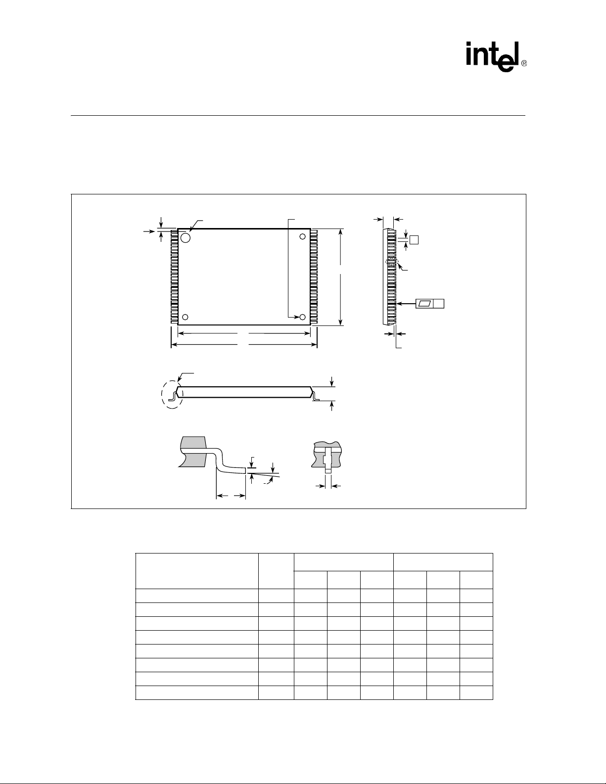
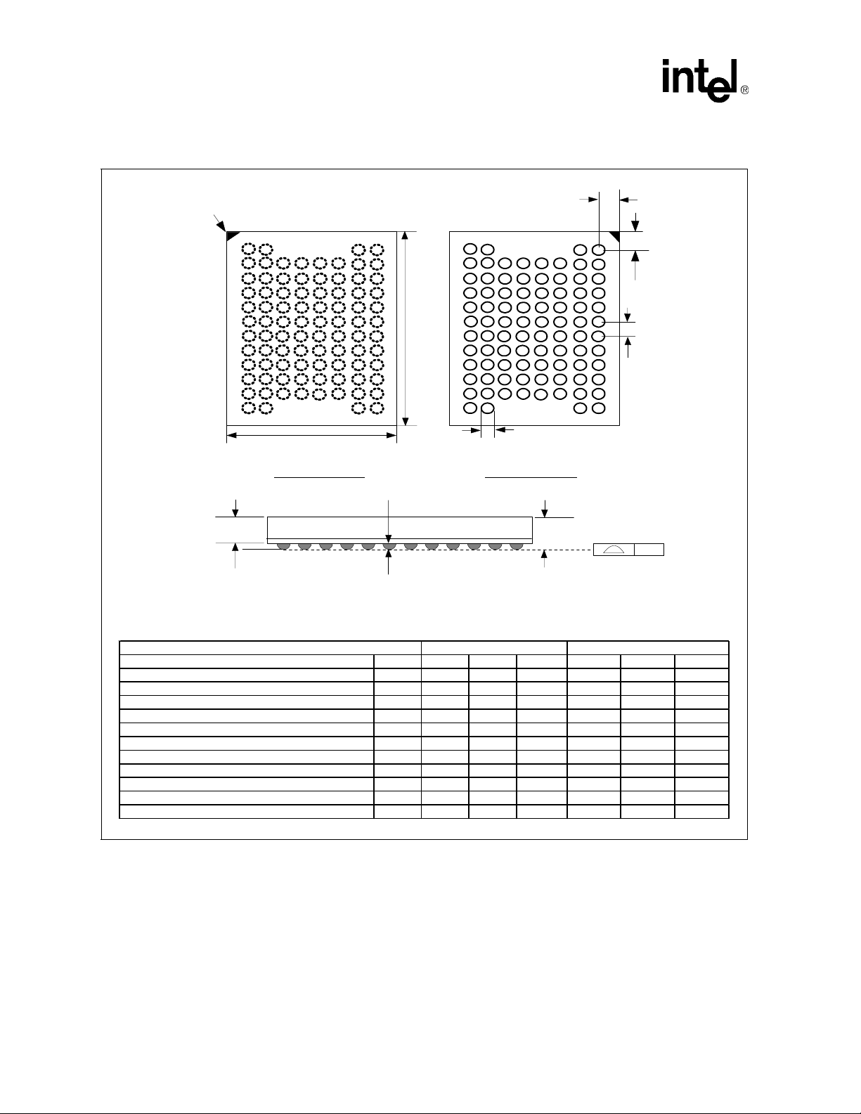
3.1 56-Lead TSOP Package
Figure 1. TSOP Mechanical Specifications
Pin 1
Z
See Notes 1 and 3
D
1
D
See Note 2
A
2
e
E
See Detail B
A
1
Seating
Plane
Y
See Detail A
A
Detail A
Detail B
C
0
L
b
Table 1. TSOP Package Dimensions (Sheet 1 of 2)
Product Information Sym
Package Height A - - 1.200 - - 0.047
Standoff A
Package Body Thickness A
Lead Width b 0.100 0.150 0.200 0.004 0.006 0.008
Lead Thickness c 0.100 0.150 0.200 0.004 0.006 0.008
Package Body Length D
Package Body Width E 13.800 14.000 14.200 0.543 0.551 0.559
Lead Pitch e - 0.500 - - 0.0197 -
1
2
1
Millimeters Inches
Min Nom Max Min Nom Max
0.050 - - 0.002 - -
0.965 0.995 1.025 0.038 0.039 0.040
18.200 18.400 18.600 0.717 0.724 0.732
April 2005 Intel StrataFlash® Embedded Memory (P30) Datasheet
10 Order Number: 306666, Revision: 001
Page 11
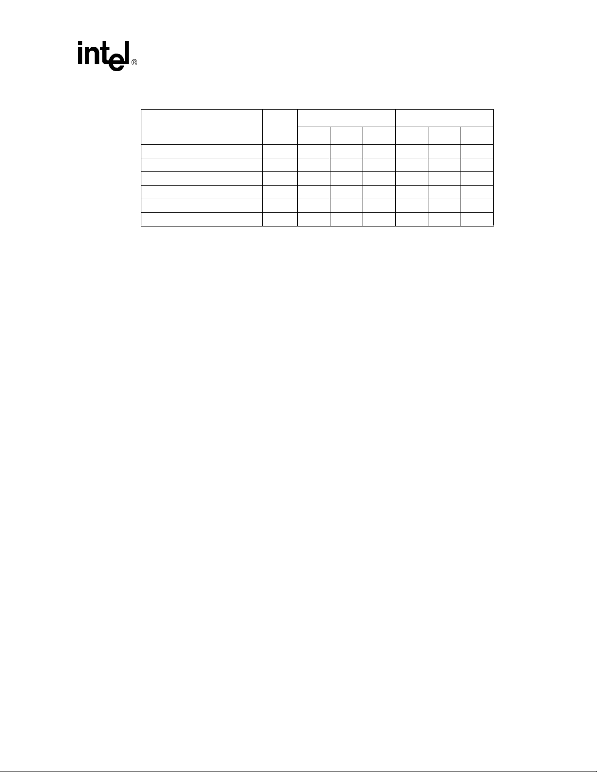
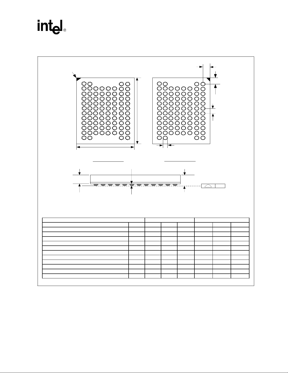
Table 1. TSOP Package Dimensions (Sheet 2 of 2)
1-Gbit P30 Family
Product In f ormation Sym
Terminal Dimension D 19.800 20.00 20.200 0.780 0.787 0.795
Lead Tip Length L 0.500 0.600 0.700 0.020 0.024 0.028
Lead Count N - 56 - - 56 Lead Tip Angle ∅ 0° 3° 5° 0° 3° 5°
Seating Plane Coplanarity Y - - 0.100 - - 0.004
Lead to Package Offset Z 0.150 0.250 0.350 0. 006 0.010 0. 014
Millimeters Inches
Min Nom Max Min Nom Max
Datasheet Intel StrataFlash® Embedded Memory (P30) April 2005
Order Number: 306666, Revision: 001 11
Page 12
1-Gbit P30 Family
3.2 64-Ball Easy BGA Package
Figure 2. Easy BGA Mechanical Specifications
Ball A1
Corner
E
A2
Ball A1
D
87654321
A
B
C
D
E
F
G
H
Top View - Ball side down Bottom View - Ball Side Up
A1
87654321
A
B
C
D
E
F
G
H
A
Seating
Plane
Note: Drawi ng not to scale
Corner
S1
S2
b
e
Y
Table 2. Easy BGA Package Dimensions
Product Informa tion
Package Height (64/128/256-Mbit)
Package Height (512-Mbit)
Ball Height (64/128/256-Mbit)
Ball Height (512-Mbit)
Package Body Thickness (64/128/256-Mbit)
Package Body Thickness (512-Mbit)
Ball (Lead) Width
Package Body Width
Package Body Length
Pitch
Ball (Lead) Count
Seating Plane Coplanarity
Corner to Ball A1 Distance Along D
Corner to Ball A1 Distance Along E
Symbol
A - - 1.200 - - 0.0472
A - - 1.300 - - 0.0512
A1 0.250 - - 0.0098 - A1 0.240 - - 0.0094 - A2 - 0.780 - - 0.0307 A2 - 0.910 - - 0.0358 -
b 0.330 0.430 0.530 0.0130 0.0169 0.0209
D 9.900 10.000 10.100 0.3898 0.3937 0.3976 1
E 12.900 13.000 13.100 0.5079 0.5118 0.5157 1
[e] - 1.000 - - 0.0394 -
N - 64 - - 64 -
Y - - 0.100 - - 0.0039
S1 1.400 1.500 1.600 0.0551 0.0591 0.0630 1
S2 2.900 3.000 3.100 0.1142 0.1181 0.1220 1
Note: Daisy Chain Evaluation Unit information is at Intel® Flash Memory Packaging Technology http://developer.intel.com/
design/flash/packtech.
Millimeters Inches
Min Nom Max Min Nom Max
Notes
April 2005 Intel StrataFlash® Embedded Memory (P30) Datasheet
12 Order Number: 306666, Revision: 001
Page 13
1-Gbit P30 Family
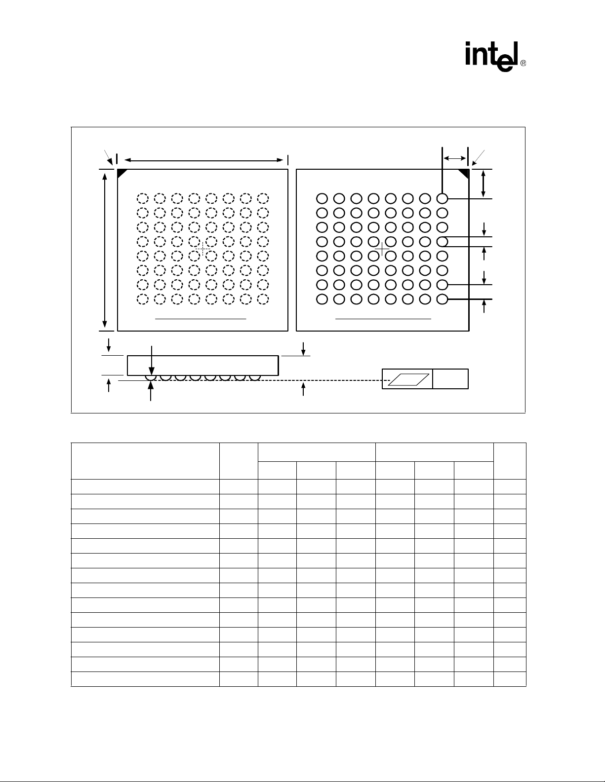
3.3 QUAD+ SCSP Packages
Figure 3. 64/128-Mbit, 88-ball (80 active) QUAD+ SCSP Specifications (8x10x1.2 mm)
A1 Index
Mark
A
B
C
D
E
F
G
H
J
K
L
M
12345678
E
Top View - Ball
A
2
Down
S
1
12345678
S
A
B
C
D
E
F
D
G
H
J
K
L
M
b
Bottom View - Ball Up
A
1
A
2
e
Y
Draw ing not to s cale.
Dimensions Symb ol Min Nom Max Min N om Max
Millimeters Inches
Package Height A - - 1.200 - - 0.0472
Ball Height A
Package Body Thickness A
1
0.200 - - 0.0079 - -
2
- 0.860 - - 0.0339 Ball (Lead) Width b 0.325 0.375 0.425 0.0128 0.0148 0.0167
Package Body Width D 9.900 10.000 10.100 0.3898 0.3937 0.3976
Package Body Length E 7.900 8.000 8.100 0.3110 0.3150 0.3189
Pitch e - 0.800 - - 0.0315 Ball (L ead) Count N - 8 8 - - 88 Seating Plane Coplanarity Y - - 0.100 - - 0.0039
Corner to Ball A1 Distance Along E S
Corner to Ball A1 Distance Along D S
1
1.100 1.200 1.300 0.0433 0.0472 0.0512
2
0.500 0.600 0.700 0.0197 0.0236 0.0276
Datasheet Intel StrataFlash® Embedded Memory (P30) April 2005
Order Number: 306666, Revision: 001 13
Page 14
1-Gbit P30 Family
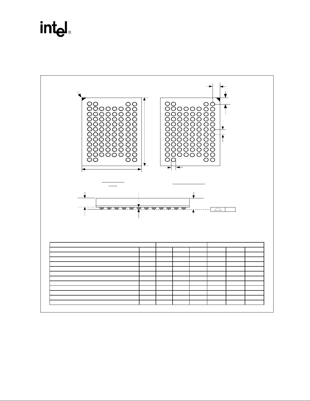
Figure 4. 256-Mbit, 88-ball (80 active) QUAD+ SCSP Specifications (8x11x1.0 mm)
A1 Index
Mark
A
B
C
D
E
F
G
H
J
K
L
M
1234 5678
E
Top View - Ball Down
A2
A1
S1
12345678
A
B
C
D
E
F
D
G
H
J
K
L
M
b
Bottom View - Ball Up
A
S2
e
Y
D raw in g not t o sc ale.
Note: Dimensions A1, A2, and b are preliminary
Dimensions Symbol Min Nom M a x Min Nom Max
Package Height A - - 1.0 00 - - 0.039 4
Ball Height A1 0.117 - - 0.0046 - Package Body Thickness A2 - 0.740 - - 0.0291 Ball (Lead) Width b 0.300 0.350 0.400 0.0118 0.0138 0.0157
Package Body Length D 10.900 11.00 11.100 0.4291 0.4331 0.4370
Package Body Width E 7.900 8.00 8.100 0.3110 0.3150 0.3189
Pitch e - 0.80 - - 0.0315 Ball (Lead) Count N - 88 - - 88 Seating Plane Coplanarity Y - - 0.1 00 - - 0.003 9
Corner to Ball A1 Distance Along E S1 1.100 1.200 1.300 0.0433 0.047 2 0.0512
Corner to Ball A1 Distance Along D S2 1.000 1.100 1.200 0.0394 0.0433 0.04 7 2
Millimeters Inches
April 2005 Intel StrataFlash® Embedded Memory (P30) Datasheet
14 Order Number: 306666, Revision: 001
Page 15
1-Gbit P30 Family
Figure 5. 512-Mbit, 88-ball (80 active) QUAD+ SCSP Specifications (8x11x1.2 mm)
A1 Index
Mark
A
B
C
D
E
F
G
H
J
K
L
M
12345678
E
Top View - Ball Down
A2
A1
S1
12345678
A
B
C
D
E
F
D
G
H
J
K
L
M
b
Bottom View -Ball Up
A
S2
e
Y
Draw ing not to s cale .
Dimensions Symbol Min Nom Max Min Nom Max
Millimeters Inches
Package Height A - - 1.200 - - 0.0472
Ball Height A1 0.200 - - 0.0079 - Package Body Thickness A2 - 0.860 - - 0.0339 Ball (Lead) Width b 0.325 0.375 0.425 0.0128 0.0148 0.0167
Package Body Length D 10.900 11.000 11.100 0.4291 0.4331 0.4370
Package Body Width E 7.900 8.000 8.100 0.3110 0.3150 0.3189
Pitch e - 0.800 - - 0.0315 B a ll (Lead) Count N - 88 - - 8 8 Seating Plane Coplanarity Y - - 0.100 - - 0.0039
C o rner to Ball A1 Distance Along E S1 1. 100 1. 200 1.30 0 0.0433 0. 0472 0. 0512
C o rner to Ball A1 Distance Along D S2 1.000 1. 100 1.20 0 0.0394 0. 0433 0. 047 2
Datasheet Intel StrataFlash® Embedded Memory (P30) April 2005
Order Number: 306666, Revision: 001 15
Page 16
1-Gbit P30 Family
Figure 6. 1-Gbit, 88-ball (80 active) QUAD+ SCSP Specifications (11x11x1.4 mm)
A1 Index
Mark
A
B
C
D
E
F
G
H
J
K
L
M
12345678
E
Top View - Ball Down
A2
S1
2345678
1
A
B
C
D
E
F
D
G
H
J
K
L
M
b
Bottom View - B a ll U p
A1
A
S2
e
Y
Drawing not to scale.
Dimens ions Symbol Min Nom Max Min N om Max
Millimeters Inches
Package Height A - - 1.400 - - 0.0551
Ball Height A1 0.200 - - 0.0079 - Package Body Thickness A2 - 1.070 - - 0.0421 Ball (Lead) Width b 0.325 0.375 0.425 0.0128 0.0148 0.0167
Package Body Length D 10.900 11.000 11.100 0.4291 0.4331 0.4370
Package Body Width E 10.900 11.000 11.100 0.4291 0.4331 0.4370
Pitch e - 0.800 - - 0.0315 Ball (Lead) Count N - 88 - - 88 Seating Plane Coplanarity Y - - 0.100 - - 0.0039
Corner to Ball A1 Distance A long E S1 2.600 2.700 2.800 0.1024 0.1063 0.1102
Corner to Ball A1 Distance A long D S2 1.000 1.100 1.200 0.0394 0.0433 0.0472
April 2005 Intel StrataFlash® Embedded Memory (P30) Datasheet
16 Order Number: 306666, Revision: 001
Page 17
4.0 Ballout and Signal Descriptions
4.1 Signal Ballout
Figure 7. 56-Lead TSOP Pinout (64/128/256-Mbit)
1-Gbit P30 Family
10
11
12
13
14
15
16
17
18
19
20
21
22
23
24
25
26
27
28
1
2
3
4
5
6
7
8
9
Intel StrataFlash®
Embedded Memory (P30)
56-Lead TSOP Pinout
14 mm x 20 mm
Top View
A16
A15
A14
A13
A12
A11
A10
A9
A23
A22
A21
VSS
VCC
WE#
WP#
A20
A19
A18
A8
A7
A6
A5
A4
A3
A2
A24
RFU
VSS
Notes:
1. A1 is the least significant addres s bit.
2. A23 is valid for 128-Mbit densities and above; otherwise, it is a no connect (NC).
3. A24 is valid for 256-Mbit densities and above; otherwise, it is a no connect (NC).
56
55
54
53
52
51
50
49
48
47
46
45
44
43
42
41
40
39
38
37
36
35
34
33
32
31
30
29
WAIT
A17
DQ15
DQ7
DQ14
DQ6
DQ13
DQ5
DQ12
DQ4
ADV#
CLK
RST#
VPP
DQ11
DQ3
DQ10
DQ2
VCCQ
DQ9
DQ1
DQ8
DQ0
VCC
OE#
VSS
CE#
A1
Datasheet Intel StrataFlash® Embedded Memory (P30) April 2005
Order Number: 306666, Revision: 001 17
Page 18
1-Gbit P30 Family
Figure 8. 64-Ball Easy BGA Ballout (64/128/256/512-Mbit)
18234567
A
A1 A6 A8 A13VPP A18 A22VCC
B
A2 VSS A9 A14CE# A19 RFUA25
C
A3 A7 A10 A15A12 A20 A21WP#
D
A4 A5 A11 VCCQRST# A16 A17VCCQ
E
F
RFU OE#DQ0 DQ10 DQ12DQ11 WAITADV#
G
H
RFU VSS VCC DQ13VSS DQ7 A24VSS
Easy BGA
Top View- Ball sid e down
RFUDQ8 DQ1 DQ9 DQ4DQ3 DQ15CLK
WE#A23 RFU DQ2 DQ5VCCQ DQ14DQ6
8
RFU DQ8DQ1DQ9DQ4 DQ3DQ15 CLK
WE# RFUDQ2DQ5 VCCQDQ14 DQ6
5
67
Easy BGA
Bottom View- Bal l s ide up
Notes:
1. A1 is the least significant address bi t.
2. A23 is valid for 128 -Mbit densities and above; other wise, it is a no connect (NC).
3. A24 is valid for 256 -Mbit densities and above; other wise, it is a no connect (NC).
4. A25 is valid for 512-Mbit densities; otherwise, it is a no connect (NC).
1
234
A
A1A6A8A13 VPPA18A22 VCC
B
A2VSSA9A14 CE#A19RFU A25
C
A3A7A10A15 A12A20A21 WP#
D
A4A5A11VCCQRST#A16A17 VCCQ
E
F
RFUOE# DQ0DQ10DQ12 DQ11WAIT ADV#
G
A23
H
RFUVSSVCCDQ13 VSSDQ7A24 VSS
April 2005 Intel StrataFlash® Embedded Memory (P30) Datasheet
18 Order Number: 306666, Revision: 001
Page 19

Figure 9. 88-Ball (80-Active Ball) QUAD+ SCSP Ballout
Pin 1
12345678
1-Gbit P30 Family
A
B
C
D
E
F
G
H
J
K
DU DU Depop Depop Depop Depop DU DU
A4 A18 A19 VSS VCC VCC A21 A11
A5 RFUA23VSSRFUCLKA22A12
A3 A17 A24 VPP RFU RFU A9 A13
A2 A7 RFU WP# ADV# A20 A10 A15
A1 A6 RFU RST# WE# A8 A14 A16
A0 DQ8 DQ2 DQ10 DQ5 DQ13 WAIT F2-CE#
RFU DQ0 DQ1 DQ3 DQ12 DQ14 DQ7 F2-OE#
RFU F1-OE# DQ9 DQ11 DQ4 DQ6 DQ15 VCCQ
F1-CE# RFU RFU RFU RFU VCC VCCQ RFU
A
B
C
D
E
F
G
H
J
K
L
M
VSS VSS VCCQ VCC VSS VSS VSS VSS
DU DU Depop Depop Depop Depop DU DU
12345678
L
M
Datasheet Intel StrataFlash® Embedded Memory (P30) April 2005
Order Number: 306666, Revision: 001 19
Page 20
1-Gbit P30 Family
4.2 Signal Descriptions
This section has signal descriptions for the various P30 packages.
Table 3. TSOP and Easy BGA Signal Descriptions (Sheet 1 of 2)
Symbol Type Name and Func tio n
ADDRESS INPUTS: Device address inputs. 64-Mbit: A[22:1]; 128-Mbit: A[23:1]; 256-Mbit: A[24:1];
A[MAX:1] Input
DQ[15:0]
Input/
Output
ADV# Input
CE# Input
CLK Input
OE# Input
RST# Input
WAIT Output
WE# Input
WP# Input
VPP
Power/
Input
VCC Power
512-Mbit: A[ 25 :1 ].
See Table 5 on page22 and Figure 10 on p age23 for 512-Mbit addressing.
DATA INPUT/OUTPUTS : Inputs data and commands during write cycles; outputs dat a during
memory, Status Register, Protection Register, and Read Configuration Register reads. Data balls
float when the CE# or OE# are deasserted. Data is in ternally latched during writes.
ADDRESS VALID: Active low input. During synchronous read operations, addresses are latched on
the rising edge of ADV#, or on the next valid CLK edge with ADV# low, whichever occurs first.
In asynchronous mode, the address is latched when ADV# going high or continuously flows through
if ADV# is held low.
WARNING: Designs not using ADV# must tie it to VSS to allow addresses to flow through.
FLASH CHIP ENABLE: Active low input. CE# low selects the associated flash memory die. When
asserted, f lash internal control logic, i nput buffers, decoders, and sen s e amplifiers are active. When
deasserted, the associated flash die is deselected, power is reduced to standby lev els, data and
WAIT outputs are placed in high-Z state.
WARNING: All chip enables must be high when device is not in use.
CLOCK: Synchronizes the device with the syste m’s bus frequency in synchronous-read mode.
During synchronous read operations, addresses ar e latched on the rising edge of ADV#, or on the
next valid CLK edge with ADV# low, whichever occurs first.
WARNING: Designs not using CLK for synchronous read mode must tie it to VCCQ or VSS.
OUTPUT ENABLE: Active low input. OE# low enables the device’s output data buffers during read
cycles. OE# high places the data outputs and W AIT in High-Z.
RESET: Active low input. RST# resets internal automation and inhibits write operations. This
provides data protection during power transitions. RST# high enables normal operation. Exit from
reset places the device in asynchronous read array mode.
WAIT: Indicates data valid in synchronous array or non-array burst reads. Read Configuration
Register bit 10 (RCR[10], WT) determines its polarity when asserted. WAIT’s active output is V
when CE# and OE# are VIL. WAIT is high-Z if CE# or OE# is VIH.
V
OH
• In synchronous arr ay or non-array read modes, WAIT indicates invalid data when asserted and
valid data when deasserted.
• In asy n ch ro nous page mo de , an d al l w rite modes, WAIT is de a s se rt e d .
WRITE ENABLE: Active low input. WE# controls writes to the device. Address and data are latc hed
on the rising edge of WE#.
WRITE PROTECT: Active low input. WP# low enables the lock-down mechanism. Blocks in lockdown cannot be unlocked with the Unlock command. WP# high overrides the lock-down function
enabling blocks to be erased or programmed using software commands.
Erase and Progr am Power: A valid voltage on this pin all ows erasing or progr amming. Memory
level of V
IH
PP
≤ V
contents cannot be altered when V
should not be attempted.
= VCC for in-system prog r am and er ase oper at ions. To accommodate resist or o r di ode dr op s
Set V
PP
from the syste m supply, the V
min to perform in-system flash modif ication. VPP may be 0 V during read operations.
can be applied to main blocks for 1000 cy cles maximum and to par ameter blocks for 2500
V
PPH
VPP can be connected to 9 V for a cumulative total not to ex ceed 80 hours. Extended use of
cycles.
this pin at 9 V may reduce block cycling capabili ty.
. Block erase and program at invalid VPP voltages
PPLK
can be as low as V
PP
Device Core Power Supply: Core (logic) source voltage. Writes to the flash array are inhibited when
≤ V
V
CC
. Operations at invalid VCC voltages should not be attempted.
LKO
min. VPP must remain abov e V
PPL
OL
or
PPL
April 2005 Intel StrataFlash® Embedded Memory (P30) Datasheet
20 Order Number: 306666, Revision: 001
Page 21
1-Gbit P30 Family
Table 3. TSOP and Easy BGA Signal Descriptions (Sheet 2 of 2)
Symbol Type Name and Function
VCCQ Power Output Power Supply: Output-driver source voltage.
VSS Power Ground: Con nect to system ground. Do not float any VSS connection.
RFU —
DU — Do Not Use: Do not connect to any other signal, or power supply; must be left floating.
NC — No Connect: No internal connection; can be driven or floated.
Reserved for Fu ture Use: Reserve d by In tel f or fu ture de vice f uncti onali ty and enh ancemen t. T hese
should be treated in the same way as a Do Not Use (DU) signal.
Table 4. QUAD+ SCSP Signal Descriptions (Sheet 1 of 2)
Symbol Type Name and Function
ADDRESS INPUTS: Device address inputs. 64-Mbit: A[21:0]; 128-Mbit: A[22:0]; 256-Mbit: A[23:0];
A[MAX:0] Input
DQ[15:0]
ADV# Input
F1-CE#
F2-CE#
CLK Input
F1-OE#
F2-OE#
RST# Input
WAIT Output
WE# Input
Input/
Output
Input
Input
512-Mbit: A[24:0].
See Table 6 on page 22, Figure 11 on page23, and Figure 12 on page 23 for 512-Mbit and 1-Gbit
addressing.
DA TA INPUT/OUTPUTS: Inputs data and command s dur in g w rit e cy c le s ; ou tp uts data dur i n g
memory, Status Register, Protection Register, and Read Configuration Register reads. Data balls
float when the CE# or OE# are deasserted. Data is internally latched during writes.
ADDRESS VALID: Active low input. During synchronous re ad operations, addresses are latched on
the rising edge of ADV#, or on the next valid CLK edge wit h AD V# low, whichever occurs first.
In asynchronous mode, the address is latched when ADV# going high or continuously flows through
if ADV# is held lo w.
WARNING: Designs not using ADV# must tie it to VSS to allow addresses to flow through.
FLASH CHIP ENABLE: Active low input . CE# low selects the associated flash memory die. When
asserted, flash internal control logic, input buffers, decod ers, and sense amplifiers are active. When
deasserted, the associated flash die is deselected , power is reduced to standby levels, data and
WAIT outputs are placed in high-Z state.
See Table 6 on page 22 for CE# assignment definitions.
WARNING: All chip enables must be high when device is not in use.
CLOCK: Synchronizes the device with the system’s bus frequency in synchronous-read mode.
During synchronous read operations, addresses are latched on the rising edge of ADV#, or on t he
next valid CLK edge with ADV# low, whichever occurs first.
WARNING: Designs not using CLK for synchronous read mode must tie it to VCCQ or VSS.
OUTPUT ENABLE: Active low input. OE# low enables the device’s output data buffers during read
cycles. OE# high places the data outpu ts and WAIT in High-Z.
F1-OE# and F2-OE # should be tied together for all densities.
RESET: Active low input. RS T# resets internal automation and inhibits write operations. This
provides data protection during power transitions. RST# high enables normal operation. Exit from
reset places th e device in asynchronous read array mode.
WAIT: Indicates data valid in synchronous array or non-ar ray burst reads. Read C onfiguration
Register bit 10 (RCR[10], WT) determines its po larity when asserted. WAIT’s active output is V
when CE# and OE# are VIL. WAIT is high-Z if CE # or O E# is VIH.
V
OH
• In synchronous array or non-array read modes, WAIT indicates inva lid data when asserted and
valid data when deasserted.
• In asynchronous page mode, and all w rite modes, WAI T is deasserted.
WRITE ENABLE: Active low in put. WE# controls writes to the device. Address and data are latched
on the rising edg e of WE#.
OL
or
Datasheet Intel StrataFlash® Embedded Memory (P30) April 2005
Order Number: 306666, Revision: 001 21
Page 22
1-Gbit P30 Family
Table 4. QUAD+ SCSP Signal Descriptions (Sheet 2 of 2)
Symbol Type Name and Func tio n
WP# Input
VPP
Power/
lnput
VCC Power
VCCQ Power Output Power Supply: Output-driver source voltage.
VSS Power Ground: Connect to system ground. Do not float any VSS connection.
RFU —
DU — Do Not Use: Do not connect to any other signal, or power supply; must be left floating.
NC — No Connect: No internal connection; can be driven or floated.
WRITE PROTECT: Active low input. WP# low enables the lock-down mechanism. Blocks in lockdown cannot be unlocked with the Unlock command. WP# high overrides the lock-down function
enabling blocks to be erased or programmed using software commands.
Erase and Progr am Power: A valid voltage on this pin all ows erasing or progr amming. Memory
level of V
IH
PP
≤ V
contents cannot be altered when V
should not be attempted.
= VCC for in-system prog r am and er ase oper at ions. To accommodate resist or o r di ode dr op s
Set V
PP
from the syste m supply, the V
min to perform in-system flash modif ication. VPP may be 0 V during read operations.
can be applied to main blocks for 1000 cy cles maximum and to par ameter blocks for 2500
V
PPH
VPP can be connected to 9 V for a cumulative total not to ex ceed 80 hours. Extended use of
cycles.
this pin at 9 V may reduce block cycling capabili ty.
. Block erase and program at invalid VPP voltages
PPLK
can be as low as V
PP
min. VPP must remain abov e V
PPL
Device Core Power Supply: Core (logic) source voltage. Writes to the flash array are inhibited when
≤ V
V
CC
. Operations at invalid VCC voltages should not be attempted.
LKO
Reserved for Future Use: Reserved by Intel for fut ure devi ce fun ctional ity a nd enha ncement. These
should be treated in the same way as a Do Not Use (DU) signa l.
PPL
4.3 SCSP Configurations
Table 5. Stacked Easy BGA Chip Select Logic
Stack Combination
1-die F1-CE# 2-die F1-CE# + A25 (V
Table 6. QUAD+ SCSP Chip Select Logic
Stack
Combination
1-die F1-CE# - - 2-die F1-CE# + A24 (V
4-die F1-CE# + A24 (V
Selected Fl ash
Die #1
Selected Flash
Die #1
) F1-CE# + A24 (VIH)- -
IL
) F1-CE# + A24 (VIH) F2-CE# + A24 (VIL) F2-CE# + A24 (VIH)
IL
) F1-CE# + A25 (VIH)
IL
Selected Flash
Die #2
Selected Flash
Die #2
Selected Fl ash
Die #3
Selected Flash
Die #4
April 2005 Intel StrataFlash® Embedded Memory (P30) Datasheet
22 Order Number: 306666, Revision: 001
Page 23
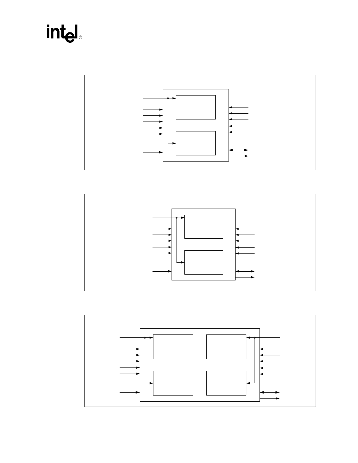
Figure 10. 512-Mbit Easy BGA Device Block Diagram
Easy BGA 2-Die (512-Mbit) Device Configuration
F1-CE#
WP#
OE#
WE#
CLK
ADV#
A[MAX:1]
Flash Die #1
(256-Mbit)
Flash Die #2
(256-Mbit)
Figure 11. 512-Mbit QUAD+ SCSP Device Block Diagram
1-Gbit P30 Family
RST#
VCC
VPP
VCCQ
VSS
DQ[15:0]
WAIT
QUAD+ 2-Die (512-Mbit) Device Configuration
F1-CE#
WP#
OE#
WE#
CLK
ADV#
Flash Die #1
(256-Mbit)
Flash Die #2
(256-Mbit)
Figure 12. 1-Gbit QUAD+ SCSP Device Block Diagram
QUAD+ 4-Die (1-Gbit) Device Configuration
F1-CE#
WP#
OE#
WE#
CLK
ADV#
Flash Die #1
(256-Mbit)
Flash Die #2
(256-Mbit)
Flash Die #3
(256-Mbit)
Flash Die #4
(256-Mbit)
RST#
VCC
VPP
VCCQ
VSS
DQ[15:0]A[MAX:0]
WAIT
F2-CE#
RST#
VCC
VPP
VCCQ
VSS
DQ[15:0]A[MAX:0]
WAIT
Datasheet Intel StrataFlash® Embedded Memory (P30) April 2005
Order Number: 306666, Revision: 001 23
Page 24

1-Gbit P30 Family
4.4 Memory Maps
Table 7 through Table 10 show the P30 memory maps. See Section 11.0, “Programming
Operations” on page 61 for Programming Region information.
Table 7. Discrete Top Parameter Memory Maps (all packages)
Programming
Region #
15
14
13
12
11
10
9
8
7
Size
Blk 256-Mbit Blk 128-Mbit
(KB)
32 258 FFC000 - FFFFFF 130 7FC000 - 7FFFFF
...
...
32 255 FF0000 - FF3FFF 127 7F0000 - FF3FFF 32 63 3F0000 - 3F3FFF
128 254 FE0000 - FEFFFF 126 7E0000 - 7EFFFF 128 62 3E0000 - 3EFFFF
...
...
128 240 F00000 - F0FFFF 120 780000 - 78FFFF 128 56 380000 - 38FFFF
128 239 EF0000 - EFFFFF 119 770000 - 77FFFF
...
...
128 224 E00000 - E0FFFF 112 700000 - 70FFFF 128 48 300000 - 30FFFF
128 223 DF0000 - DFFFFF 111 6F0000 - 6FFFFF
...
...
128 208 D00000 - D0FFFF 104 680000 - 68FFFF 128 40 280000 - 28FFFF
128 207 CF0000 - CFFFFF 103 670000 - 67FFFF
...
...
128 192 C00000 - C0FFFF 96 600000 - 60FFFF 128 32 200000 - 20FFFF
128 191 BF0000 - BFFFFF 95 5F0000 - 5FFFFF
...
...
128 176 B00000 - B0FFFF 88 580000 - 58FFFF 128 24 180000 - 18FFFF
128 175 AF0000 - AFFFFF 87 570000 - 57FFFF
...
...
128 160 A0000 - A0FFFF 80 500000 - 50FFFF 128 16 100000 - 10FFFF
128 159 9F0000 - 9FFFFF 79 4F0000 - 4FFFFF
...
...
128 144 900000 - 90FFFF 72 480000 - 48FFFF 128 8 080000 - 08FFFF
128 143 8F0000 - 8FFFFF 71 470000 - 47FFFF
...
...
128 128 800000 - 80FFFF 64 400000 - 40FFFF 128 0 000000 - 00FFFF
128 127 7F0000 - 7FFFFF 63 3F0000 - 3FFFFF
...
...
128 112 700000 - 70FFFF 56 380000 - 38FFFF
...
...
...
...
...
...
...
...
...
...
...
...
...
...
...
...
...
...
...
...
...
...
...
...
...
...
...
...
...
...
Programming
Region #
7
6
5
4
3
2
1
0
Size
Blk 64-Mbit
(KB)
32 66 3FC 000 - 3FFFFF
...
...
...
...
128 55 370000 - 37FFFF
...
...
128 47 2F0000 - 2FFFFF
...
...
128 39 270000 - 27FFFF
...
...
128 31 1F0000 - 1FFFFF
...
...
128 23 170000 - 17FFFF
...
...
128 15 0F0000 - 0FFFFF
...
...
128 7 070000 - 07FFFF
...
...
...
...
...
...
...
...
...
...
...
April 2005 Intel StrataFlash® Embedded Memory (P30) Datasheet
24 Order Number: 306666, Revision: 001
Page 25
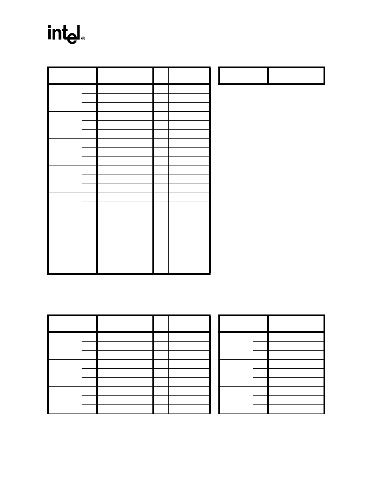
Table 7. Discrete Top Parameter Memory Maps (all packages)
1-Gbit P30 Family
Programming
Region #
6
5
4
3
2
1
0
Size
Blk 256-Mbit Blk 128-Mbit
(KB)
128 111 6F0000 - 6FFFFF 55 370000 - 37FFFF
...
...
128 96 600000 - 60FFFF 48 300000 - 30FFFF
128 95 5F0000 - 5FFFFF 47 2F0000 - 2FFFFF
...
...
128 80 500000 - 50FFFF 39 280000 - 28FFFF
128 79 4F0000 - 4FFFFF 38 270000 - 27FFFF
...
...
128 64 400000 - 40FFFF 32 200000 - 20FFFF
128 63 3F0000 - 3FFFFF 31 1F0000 - 1FFFFF
...
...
128 48 300000 - 30FFFF 24 180000 - 18FFFF
128 47 2F0000 - 2FFFFF 23 170000 - 17FFFF
...
...
128 32 200000 - 20FFFF 16 100000 - 10FFFF
128 31 1F0000 - 1FFFFF 15 0F0000 - 0FFFFF
...
...
128 16 100000 - 10FFFF 8 080000 - 08FFFF
128 15 0F0000 - 0FFFFF 7 070000 - 07FFFF
...
...
128 0 000000 - 00FFFF 0 000000 - 00FFFF
...
...
...
...
...
...
...
...
...
...
...
...
...
...
...
...
...
...
...
...
...
Programming
Region #
Size
Blk 64-Mbit
(KB)
Table 8. Discrete Bottom Parameter Memory Maps (all packages)
Programming
Region
15
14
13
Size
Blk 256-Mbit Blk 128-Mbit
(KB)
128 258 FF0000 - FFFFFF 130 7F0000 - 7FFFFF
...
...
128 243 F00000 - F0FFFF 123 780000 - 78FFFF 128 56 380000 - 38FFFF
128 242 EF0000 - EFFFFF 122 770000 - 77FFFF
...
...
128 227 E00000 - E0FFFF 115 700000 - 70FFFF 128 48 300000 - 30FFFF
128 226 DF0000 - DFFFFF 114 6F0000 - 6FFFFF
...
...
128 211 D00000 - D0FFFF 107 680000 - 68FFFF 128 40 280000 - 28FFFF
...
...
...
...
...
...
...
...
...
Programming
Region
7
6
5
Size
Blk 64-Mbit
(KB)
128 62 3F0000 - 3FFFFF
...
...
128 55 370000 - 37FFFF
...
...
128 47 2F0000 - 2FFFFF
...
...
...
...
...
Datasheet Intel StrataFlash® Embedded Memory (P30) April 2005
Order Number: 306666, Revision: 001 25
Page 26

1-Gbit P30 Family
Table 8. Discrete Bottom Parameter Memory Maps (all packages)
Programming
Region
12
11
10
9
8
7
6
5
4
3
2
1
Size
Blk 256-Mbit Blk 128-Mbit
(KB)
128 210 CF0000 - CFFFFF 106 670000 - 67FFFF
...
...
128 195 C00000 - C0FFFF 99 600000 - 60FFFF 128 32 200000 - 20FFFF
128 194 BF0000 - BFFFFF 98 5F0000 - 5FFFFF
...
...
128 179 B00000 - B0FFFF 91 580000 - 58FFFF 128 24 180000 - 18FFFF
128 178 AF0000 - AFFFFF 90 570000 - 57FFFF
...
...
128 163 A0000 - A0FFFF 83 500000 - 50FFFF 128 16 100000 - 10FFFF
128 162 9F0000 - 9FFFFF 82 4F0000 - 4FFFFF
...
...
128 147 900000 - 90FFFF 75 480000 - 48FFFF 128 8 080000 - 08FFFF
128 146 8F0000 - 8FFFFF 74 470000 - 47FFFF
...
...
128 131 800000 - 80FFFF 67 400000 - 40FFFF 128 4 010000 - 01FFFF
128 130 7F0000 - 7FFFFF 66 3F0000 - 3FFFFF 32 3 00C000 - 00FFFF
...
...
128 115 700000 - 70FFFF 59 380000 - 38FFFF 32 0 000000 - 003FFF
128 114 6F0000 - 6FFFFF 58 370000 - 37FFFF
...
...
128 99 600000 - 60FFFF 51 300000 - 30FFFF
128 98 5F0000 - 5FFFFF 50 2F0000 - 2FFFFF
...
...
128 83 500000 - 50FFFF 43 280000 - 28FFFF
128 82 4F0000 - 4FFFFF 42 270000 - 27FFFF
...
...
128 67 400000 - 40FFFF 35 200000 - 20FFFF
128 66 3F0000 - 3FFFFF 34 1F0000 - 1FFFFF
...
...
128 51 300000 - 30FFFF 27 180000 - 18FFFF
128 50 2F0000 - 2FFFFF 26 170000 - 17FFFF
...
...
128 35 200000 - 20FFFF 19 100000 - 10FFFF
128 34 1F0000 - 1FFFFF 18 0F0000 - 0FFFFF
...
...
128 19 100000 - 10FFFF 11 080000 - 08FFFF
...
...
...
...
...
...
...
...
...
...
...
...
...
...
...
...
...
...
...
...
...
...
...
...
...
...
...
...
...
...
...
...
...
...
...
...
Programming
Region
4
3
2
1
0
Size
Blk 64-Mbit
(KB)
128 39 270000 - 27FFFF
...
...
128 31 1F0000 - 1FFFFF
...
...
128 23 170000 - 17FFFF
...
...
128 15 0F0000 - 0FFFFF
...
...
128 10 070000 - 07FFFF
...
...
...
...
...
...
...
...
...
...
April 2005 Intel StrataFlash® Embedded Memory (P30) Datasheet
26 Order Number: 306666, Revision: 001
Page 27
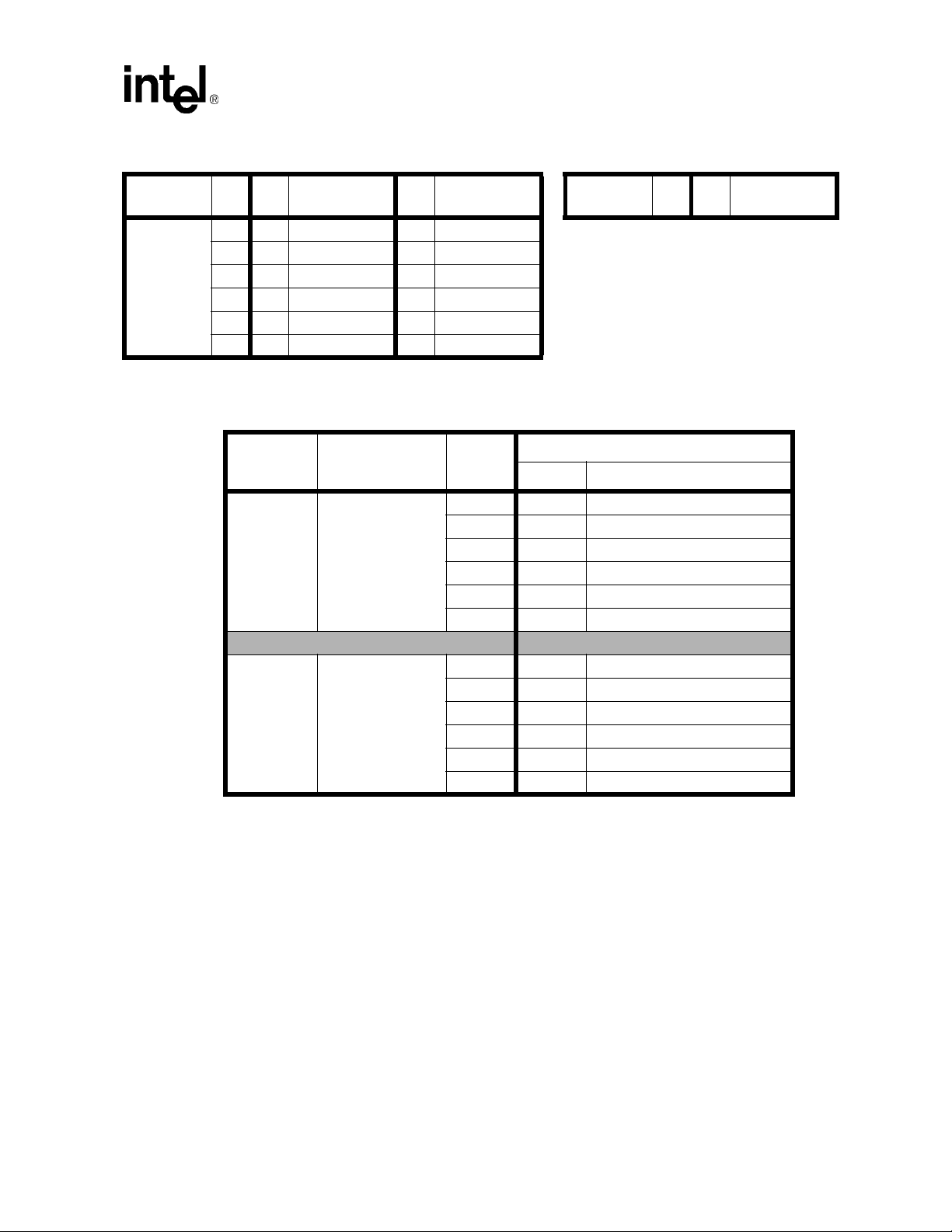
Table 8. Discrete Bottom Parameter Memory Maps (all packages)
1-Gbit P30 Family
Programming
Region
0
Size
Blk 256-Mbit Blk 128-Mbit
(KB)
128 18 0F0000 - 0FFFFF 10 070000 - 07FFFF
...
...
128 4 010000 - 01FFFF 4 010000 - 01FFFF
32 3 00C000 - 00FFFF 3 00C000 - 00FFFF
...
...
32 0 000000 - 03FFFF 0 000000 - 00FFFF
...
...
...
...
...
...
Programming
Region
Table 9. 512-Mbit Memory Map (Easy BGA and QUAD+ SCSP)
Flash Die # Die Stack Config. Size (KB)
32 258 FFC000 - FFFFFF
...
2
Flash Die #2
(Top Parameter)
32 255 FF0000 - FF3FFF
128 254 FE0000 - FEFFFF
...
128 0 000000 - 00FFFF
512-Mbit Flash (2x256-Mbit w/ 1CE)
Blk Address Rang e
...
...
Size
Blk 64-Mbit
(KB)
...
...
128 258 FF0000 - FFFFFF
...
1
Note: Refer to 256-Mbit Memory Map (Tabl e 7 and Table 8) for Pr ogramming Region Information.
Flash Die #1 (Bott om
Parameter)
128 4 010000 - 01FFFF
32 3 00C000 - 00FFFF
...
32 0 000000 - 003FFF
...
...
...
...
Datasheet Intel StrataFlash® Embedded Memory (P30) April 2005
Order Number: 306666, Revision: 001 27
Page 28
1-Gbit P30 Family
Table 10. 1-Gbit Memory Map (QUAD+ SCSP o nly)
Flash Die # Die Stack Config. Size (KB)
32 258 FFC000 - FFFFFF
...
4
3
2
Flash Die #4
(Top Parameter)
Flash Die #3
(Bottom Parameter)
Flash Die #2
(Top Parameter)
32 255 FF0000 - FF3FFF
128 254 FE0000 - FEFFFF
...
128 0 000000 - 00FFFF
128 258 FF0000 - FFFFFF
...
128 5 020000 - 02FFFF
32 3 00C000 - 00FFFF
...
32 0 000000 - 003FFF
32 258 FFC000 - FFFFFF
...
32 255 FF0000 - FF3FFF
128 254 FE0000 - FEFFFF
...
1-Gbit Flash (4x256-Mbit w/ 2CE)
Blk Address Range
...
...
...
...
...
...
...
...
...
...
...
...
128 0 000000 - 00FFFF
128 258 FF0000 - FFFFFF
...
1
Note: Refer to 256-Mbit Memory Map (Table 7 and Table 8) for Programming Region Information.
Flash Die #1
(Bottom Parameter)
128 4 010000 - 01FFFF
32 3 00C000 - 00FFFF
...
32 0 000000 - 003FFF
...
...
...
...
April 2005 Intel StrataFlash® Embedded Memory (P30) Datasheet
28 Order Number: 306666, Revision: 001
Page 29
1-Gbit P30 Family
5.0 Maximum Ratings and Operating Conditions
5.1 Absolute Maximum Ratings
Warning: Stressing the device beyond the “Absolute Maximum Ratings” may cause permanent damage.
These are stress ratings only.
Parameter Maximum Rating Notes
Temperat ur e under bias –40 °C to +85 °C 1
Storage temperatur e –65 °C to +125 °C
Voltage on any signal (except VCC, VPP) –0.5 V to +4.1 V 2
VPP voltage –0.2 V to +10 V 2,3,4
VCC voltage –0.2 V to +2.5 V 2
VCCQ voltage –0.2 V to +4.1 V 2
Output short circuit current 100 mA 5
Notes:
1. Temperature for 1-Gbit SCSP is –30 °C to +85 °C.
2. Voltages shown are specifie d with respect to V
signals and –0.2V on V
periods < 20 ns. Maximum DC voltage on V
overshoot to V
+ 0.5V, which, during transitions, may overshoot to V
is V
3. Maximum DC voltage on V
4. Program/erase voltage is typically 1.7 V – 2.0 V. 9.0 V can be applied for 80 hours maximum total, to
5. Output shorted for no mor e than one second. No more than one output shorted at a time.
CCQ
any blocks for 1000 cycles maximum. 9.0 V program/erase voltage may reduce block cycling
capability.
+ 2.0 V for periods < 20 ns. Maximum DC voltage on input/output signals and V
CC
, V
CC
, and VPP. During transitions, this level may undershoot to –2.0 V for
CCQ
may overshoot to +11.5 V for perio ds < 20 ns.
PP
. Minimum DC voltage is –0.5 V on input/output
SS
is VCC + 0.5 V, w hich, during transitions, may
CC
+ 2.0 V for periods < 20 ns.
CCQ
CCQ
Datasheet Intel StrataFlash® Embedded Memory (P30) April 2005
Order Number: 306666, Revision: 001 29
Page 30

1-Gbit P30 Family
5.2 Operating Conditions
Note: Operation beyond the “Operating Conditions” is not recommended and extended exposure beyond
the “Operating Conditions” may affect device reliability.
Table 11. Operating Conditions
Symbol Parameter Min Max Units Notes
Operating Temperat u re –40 +85 °C 1,2
T
C
V
V
V
V
t
Block
Erase
Cycles
NOTES:
1. T
2. Temperature for 1-Gbit SCSP is –30 °C to +85 °C.
3. In typical operation, the VPP program voltage is V
VCC Supply Voltage 1.7 2.0
CC
I/O Supply Voltage
CCQ
PPLVPP
PPH
PPH
Volt age Supply (Logic Level) 0.9 3.6
Factory word programming V
Maximum VPP Hours VPP = V
Main and Parameter Blocks V
Parameter Blocks V
= Case Temperature
C
hours.
CMOS inputs 1.7 3 .6
TTL inputs 2.4 3.6
PP
PPH
= V
PP
CC
= V
PP
PPH
= V
PP
PPH
. VPP can be connected to 8.5 V – 9.5 V for 80
PPL
V
8.5 9.5
-80Hours
100,000 -
-1000
CyclesMain Blocks V
-2500
3
April 2005 Intel StrataFlash® Embedded Memory (P30) Datasheet
30 Order Number: 306666, Revision: 001
Page 31

6.0 Electrical Specifications
6.1 DC Current Characteristics
Table 12. DC Current Characteristics (Sheet 1 of 2)
1-Gbit P30 Family
Sym Parameter
Input Load Current - ±1 - ±2 µA
I
LI
Output
I
I
CCS
I
CCD
LO
Leakage
Current
,
V
CC
Power Down
DQ[15:0], WAIT - ± 1 - ±10 µA
Standby,
Asynchronou s SingleWord f = 5 MHz (1 CLK)
Page-Mode Read
I
CCR
Average
V
CC
Read
Current
f = 13 MHz (5 CLK)
Synchronous Burst
f = 40 MHz
V
I
CCW,
I
CCE
Program Current,
CC
V
Erase Current
CC
VCC Program
I
I
CCWS,
I
CCES
I
PPS,
PPWS,
I
PPES
I
PPRVPP
Suspend Current,
Erase
V
CC
Suspend Current
V
St andby Current,
PP
V
Program Suspend Current,
PP
V
Erase Suspend Current
PP
Read 2 15 2 15 µA VPP ≤ V
CMOS
Inputs
(V
CCQ
1.7 V - 3.6 V)
=
TTL Inputs
=
(V
CCQ
2.4 V - 3.6 V)
Typ Max Typ Max
64-Mbit20352035
128-Mbit 30 75 30 75
256-Mbit 55 115 55 200
512-Mbit 110 230 110 400
1-Gbit 220 460 220 800
14 16 14 16 mA
910910mA
13 17 n/a n/a mA BL = 4W
15 19 n/a n/a mA BL = 8W
17 21 n/a n/a mA BL = 16W
21 26 n/a n/a mA BL = Cont.
36 51 36 51
26 33 26 33 V
64-Mbit20352035
128-Mbit 30 75 30 75
256-Mbit 55 115 55 200
512-Mbit 110 230 110 400
1-Gbit 220 460 220 800
0.2 5 0.2 5 µA V
Unit Test Conditions Notes
V
= VCCMax
CC
= V
= V
= V
CCQ
CCQ
CCQ
CCQ
CCQ
CCQ
IH
CCQ
SS
Max
or V
Max
or V
Max
(for I
(for I
SS
SS
CCD
CCS
1
)
1,2
)
V
V
VCC = VCCMax
V
V
V
V
CE# = V
µA
RST# = V
RST# = V
WP# = V
CCQ
= V
IN
CCQ
= V
IN
= VCCMax
CC
CCQ
1-Word
Read
mA
µA
4-Word
Read
V
= V
PP
= V
PP
CE# = V
progress
= V
PP
PPL
PPH
CCQ
PPL
CC
= VCCMax
V
CC
CE# = V
OE# = V
Inputs: VIL or V
IL
IH
1
IH
, pgm/ers in progress 1,3,4,7
, pgm/ers in progress 1,3,5,7
; suspend in
1,3,6
, suspend in progress 1,3
1,3
Datasheet Intel StrataFlash® Embedded Memory (P30) April 2005
Order Number: 306666, Revision: 001 31
Page 32

1-Gbit P30 Family
Table 12. DC Current Characteristics (Sheet 2 of 2)
Sym Parameter
CMOS
Inputs
(V
CCQ
1.7 V - 3.6 V)
=
TTL Inputs
(V
2.4 V - 3.6 V)
Typ Max Typ Max
I
PPWVPP
I
PPEVPP
Program Current
Erase Current
0.05 0.10 0.05 0.10
822822 V
0.05 0.10 0.05 0.10
822822 V
Notes:
1. All currents are RMS unless noted. Typical values at typical V
2. I
3. Sampled, not 100% tested.
4. V
5. V
6. I
7. I
is the average cur rent measured over any 5 ms time interval 5 µs after CE# is deasserted.
CCS
read + program current is the sum of VCC read and VCC program currents.
CC
read + erase current is the sum of VCC read and VCC erase currents.
CC
is specified with the device des elected. If devic e is read while in erase suspend, current is I
CCES
, I
CCW
page 45.
measured over ty pical or max times specified in Section 7.5, “Program and Erase Characte ristics” on
CCE
6.2 DC Voltage Characteristics
Table 13. DC Voltage Characteristics
CMOS Inputs
= 1.7 V - 3.6 V)
(V
Sym Parameter
CCQ
Min Max Min Max
Input Low Voltage 0 0.4 0 0.6 V
V
IL
V
IH
V
OL
V
OH
V
PPLKVPP
V
LKOVCC
V
LKOQVCCQ
Input High Volta ge V
Output Low Voltage - 0.1 - 0.1 V
Output High Voltage V
Lock-Out Voltage - 0.4 - 0.4 V 3
Lock Voltage 1.0 - 1.0 - V
Lock Voltage 0.9 - 0.9 - V
– 0.4 V
CCQ
– 0.1 - V
CCQ
CCQ
NOTES:
1. Synchronous read mode is not supported with TTL inputs.
2. V
3. V
can undershoot to –0.4 V and VIH can overshoot to V
IL
PP
≤ V
inhibits erase and program operations. Do not use V
PPLK
(V
CCQ
CCQ
CCQ
=
CCQ
TTL Inputs
= 2.4 V - 3.6 V)
2.0 V
Unit Test Conditions Notes
V
= V
PP
mA
mA
, TC = +25 °C.
CC
(1)
PPL,
= V
PP
PPH,
V
= V
PP
PPL,
= V
PP
PPH,
Unit Test Condition No tes
CCQ
V
– 0.1 - V
+ 0.4 V for durations of 20 ns or less.
PPL
and V
outside their valid ranges.
PPH
program in progress
program in progress
erase in progress
erase in progress
plus I
CCES
V
= VCCMin
CC
= V
= V
CCQ
CCQ
Min
Min
V
CCQ
= 100 µA
I
OL
V
= VCCMin
CC
V
CCQ
= –100 µA
I
OH
CCR
.
2
April 2005 Intel StrataFlash® Embedded Memory (P30) Datasheet
32 Order Number: 306666, Revision: 001
Page 33

7.0 AC Characteristics
V
7.1 AC Test Conditions
Figure 13. A C Input/Output Reference Waveform
CCQ
1-Gbit P30 Family
Input V
Note: AC test inpu ts are driven at V
/2. Input rise and fall times (10% to 90%) < 5 ns. Worst case speed occurs at VCC = VCCMin.
at V
CCQ
/2 V
CCQ
CCQ
Test Points
for Logic "1" and 0.0 V for Logic "0." Input/output timing begins/ends
CCQ
Figure 14. Transient Equivalent Testing Load Circuit
Device
Under Test
C
L
NOTES:
1. See the following table for component values.
2. Test configuration component value for worst case speed conditions.
.
3. C
includes jig capacitance
L
Out
Table 14. Test configuration component value for worst case speed conditions
Test Configurat ion CL (pF)
Min Standard Test 30
V
CCQ
Figure 15. Clock Input AC Waveform
/2 Output
R201
V
IH
CLK [C]
V
IL
R203R202
Datasheet Intel StrataFlash® Embedded Memory (P30) April 2005
Order Number: 306666, Revision: 001 33
Page 34

1-Gbit P30 Family
7.2 Capacitance
Table 15. Capacitance
Symbol Parameter Signals Min Typ Max Unit Condition Note
Address, Data,
C
Input Capacitance
IN
C
NOTES:
1. Capacitance values are for a single die; for 2-die and 4-die stacks multiple the above value s by the number of die in the
2. Sampled, not 100% tested.
3. S il ic o n die capacitan c e only, add 1 pF for discret e pac k a ges.
Output Capacitance Data, WAIT 2 4 5 pF
OUT
stack.
CE#, WE#, OE#,
RST#, CLK,
ADV#, WP#
26 7 pF
Typ temp = 25 °C,
Max temp = 85 °C,
= V
V
CC
Discrete silicon die
= (0 V - 1.95 V),
CCQ
1,2,3
April 2005 Intel StrataFlash® Embedded Memory (P30) Datasheet
34 Order Number: 306666, Revision: 001
Page 35

1-Gbit P30 Family
7.3 AC Read Specifications
Table 16. AC Read Specifications for 64/128-Mbit Densities (Sheet 1 of 2)
Num Symbol Parameter Min Max Unit Notes
Asynchronous Specificati ons
R1 t
R2
R3
R4
R5 t
R6 t
R7 t
R8 t
R10 t
R11 t
R12 t
R13 t
R15 t
R16
R17
AVAV
t
AVQV
t
ELQV
t
GLQV
PHQV
ELQX
GLQX
EHQZ
GHQZ
EHEL
ELTV
EHTZ
GLTV
t
GLTX
t
GHTZ
OH
Latching S pecifications
R101 t
R102 t
R103 t
R104 t
R105 t
R106 t
R108 t
R111 t
AVVH
ELVH
VLQV
VLVH
VHVL
VHAX
APA
phvh
Clock Specif ica t i on s
R200 f
R201 t
R202 t
R203 t
CLK
CLK
CH/CL
FCLK/RCLK
Synchronous Specifications
R301 t
R302 t
R303 t
R304 t
CHQV
AVCH/L
VLCH/L
ELCH/L
/ t
Read cycle time 85 - ns
Address to output valid - 85 ns
CE# low to output valid - 85 ns
OE# low to output valid - 25 ns 1,2
RST# high to output valid - 150 ns 1
CE# low to output in low-Z 0 - ns 1,3
OE# low to output in low-Z 0 - ns 1,2, 3
CE# high to output in high-Z - 24 ns
OE# high to output in high-Z - 24 ns
Output hold from first occurring address, CE#, or OE# change 0 - ns
CE# pulse width high 20 - ns
CE# low to W A IT valid - 17 ns
CE# high to WAIT high-Z - 20 ns 1,3
OE# low to WAIT vali d - 17 ns 1
OE# low to WAIT in low-Z 0 - ns
OE# high to WAIT in high-Z - 20 ns
Address setup to ADV# high 10 - ns
CE# low to ADV# high 10 - ns
ADV# low to output valid - 85 ns
ADV# pulse width low 10 - ns
ADV# pulse width high 10 - ns
Address hold from ADV# high 9 - ns 1,4
Page address access - 25 ns
RST# high to ADV# high 30 - ns
CLK frequency - 40 MHz
CLK period 25 - ns
CLK high/low time 5 - ns
CLK fall/ri se ti me - 3 ns
Address setup to CLK 9 - ns
ADV# low setup to CLK 9 - ns
CE# low setup to CLK 9 - ns
CLK to output valid - 20 ns
CLQV
1,3R9 t
1
1,3
1
1
1,3,6
1
Datasheet Intel StrataFlash® Embedded Memory (P30) April 2005
Order Number: 306666, Revision: 001 35
Page 36

1-Gbit P30 Family
Table 16. AC Read Specifications for 64/128-Mbit Densities (Sheet 2 of 2)
Num Symbol Parameter Min Max Unit Notes
R305 t
R306 t
R307 t
R311 t
R312 t
CHQX
CHAX
CHTV
CHVL
CHTX
Output hold from CLK 3 - ns 1,5
Address hold from CLK 10 - ns 1,4,5
CLK to WAIT valid - 20 ns 1,5
CLK Valid to ADV# Setup 3 - ns 1
WAIT Hold from CLK 3 - ns 1,5
NOTES:
1. See Figure 13, “A C Inpu t/ Out pu t Ref erenc e Waveform” on p age33 for timing measurements and max allowable input
slew rate.
– t
2. OE# may be delayed by up to t
3. Sampled, not 100% tested.
ELQV
4. Address hold in synchr onous burst mode is t
5. Applies only to subsequent synchronou s reads.
after CE#’s falling edge without impact to t
GLQV
CHAX
or t
, whichever timing specification is satisfied first.
VHAX
ELQV
.
6. See your local Intel representative for designs requiring higher than 40 MHz synchronous operation.
Table 17. AC Read Specifications for 256/512-Mbit and 1-Gbit Densities (Sheet 1 of 2)
Num Symbol Parameter Speed Min Max Unit Notes
Asynchronous Specifications
R1 t
R2
R3
R4
R5 t
R6 t
R7 t
R8 t
R10 t
R11 t
R12 t
R13 t
R15 t
R16
R17
AVAV
t
AVQV
t
ELQV
t
GLQV
PHQV
ELQX
GLQX
EHQZ
GHQZ
EHEL
ELTV
EHTZ
GLTV
t
GLTX
t
GHTZ
OH
Read cycle time
Address to output valid
CE# low to output valid
OE# low to output valid - 25 ns 1,2
RST# high to output valid - 150 ns 1
CE# low to output in low-Z 0 - ns 1,3
OE# low to output in low-Z 0 - ns 1,2,3
CE# high to output in high-Z - 24 ns
OE# high to output in high-Z - 24 ns
Output hold from first occurring address, CE#, or OE# change 0 - ns
CE# pulse width high 20 - ns
CE# low to WAIT val i d - 17 ns
CE# high to WAIT high-Z - 20 ns 1,3
OE# low to WAIT valid - 17 ns 1
OE# low to WAIT in low-Z 0 - ns
OE# high to WAIT in high-Z - 20 ns
Latching Specifications
Vcc = 1.8 V
Vcc = 1.7 V
Vcc = 1.8 V
Vcc = 1.7 V
Vcc = 1.8 V
Vcc = 1.7 V
– 2.0 V 85 -
– 2.0 V 88 -
– 2.0 V -85
– 2.0 V -88
– 2.0 V -85
– 2.0 V -88
ns
ns
ns
1,3R9 t
1
1,3
April 2005 Intel StrataFlash® Embedded Memory (P30) Datasheet
36 Order Number: 306666, Revision: 001
Page 37

1-Gbit P30 Family
Table 17. AC Read Specifications for 256/512-Mbit and 1-Gbit Densities (Sheet 2 of 2)
Num Symbol Parameter Speed Min Max Unit Notes
R101 t
R102 t
R103 t
R104 t
R105 t
R106 t
R108 t
R111 t
AVVH
ELVH
VLQV
VLVH
VHVL
VHAX
APA
phvh
Clock Specif ica t i on s
R200 f
R201 t
R202 t
R203 t
CLK
CLK
CH/CL
FCLK/RCLK
Synchronous Specifications
R301 t
R302 t
R303 t
R304 t
R305 t
R306 t
R307 t
R311 t
R312 t
CHQV
AVCH/L
VLCH/L
ELCH/L
/ t
CHQX
CHAX
CHTV
CHVL
CHTX
NOTES:
1. See Figure 13, “AC Input/Output Reference Waveform” on page 33 for timing measurements and max allowable input
slew rate.
2. OE# may be delayed by up to t
3. Sampled, not 100% tested.
4. Address hold in synchronous burst mode is t
5. Applies only to subsequent synchronous reads.
6. See your local Intel rep resentative for designs requiring higher than 40 MHz synchronous operation.
Address setup to ADV# high 10 - ns
CE# low to ADV# high 10 - ns
ADV# low to output valid
Vcc = 1.8 V
Vcc = 1.7 V
– 2.0 V -85
– 2.0 V -88
ADV# pulse width low 10 - ns
ADV# pulse width high 10 - ns
Address hold from ADV# high 9 - ns 1,4
Page address access - 25 ns
RST# high to ADV# high 30 - ns
CLK frequency - 40 MHz
CLK period 25 - ns
CLK high/low time 5 - ns
CLK fall/ri se ti me - 3 ns
Address setup to CLK 9 - ns
ADV# low setup to CLK 9 - ns
CE# low setup to CLK 9 - ns
CLK to output valid - 20 ns
CLQV
Output hold from CLK 3 - ns 1,5
Address hold from CLK 10 - ns 1,4,5
CLK to WAIT valid - 20 ns 1,5
CLK Valid to ADV# Setup 3 - ns 1
WAIT Hold from CLK 3 - ns 1,5
– t
ELQV
after CE#’s falling edge without impact to t
GLQV
CHAX
or t
, whichever timing specification is satisfied first.
VHAX
ELQV
.
ns
1
1
1,3,6
1
Datasheet Intel StrataFlash® Embedded Memory (P30) April 2005
Order Number: 306666, Revision: 001 37
Page 38

1-Gbit P30 Family
A
A
Figure 16. Asynchronous Single-Word Read (ADV# Low)
R1R2R1
ddress [A]
ADV#
CE# [E}
OE# [G]
WAIT [T]
R7
R6
Data [D/Q]
R8R3
R9R4
R17R15
R5
RST# [P ]
Note: WAIT shown deasserted during asynchronou s read mode (RCR[10]=0, Wait asserted low).
Figure 17. Asynchronous Single-Word Read (ADV# Latc h)
R2
ddress [A]
A[1:0][A ]
R101
R105R105
ADV#
CE# [E}
OE# [G]
WAIT [T]
Data [D/Q]
R106
R7
R6
R1
R8R3
R9R4
R17R15
R10
Note: WAIT shown deasserted during asynchronou s read mode (RCR[10]=0, Wait asserted low).
April 2005 Intel StrataFlash® Embedded Memory (P30) Datasheet
38 Order Number: 306666, Revision: 001
Page 39

Figure 18. Asynchronous Page-Mode Read Timing
A
A
1-Gbit P30 Family
R2
R1R1
[Max:2 ] [A ]
A[1:0]
R101
R105R105
R106
ADV#
R8R3
CE# [E]
R10R4
OE# [G]
R17R15
WAIT [T ]
R108
R9R7
DATA [D/Q]
Note: WAIT shown deasserted during asynchronous read mode (RCR[10]=0, Wait asserted low).
Figure 19. Synchronous Single-Word Array or Non-array Read Timing
R102
R306R301
R2
R106R101
R3
R4
R8
R9R7
R17R307R15
R312
R305R304
CLK [ C]
ddress [A]
R105R105
ADV# [V]
CE# [ E ]
OE# [G]
WAIT [T]
Data [D/Q]
1. WAIT is dri ven per OE # a ssert io n duri ng sync hron ous ar ray or non- a rra y rea d, a nd can be co nf igu red to
R303
R104
R104
assert either during or one dat a cycle before valid data.
2. This diagram illustrates the case in which an n-word burst is initiated to the flash memory array and it is
terminated by CE# deassertion after the first word in the burst.
Datasheet Intel StrataFlash® Embedded Memory (P30) April 2005
Order Number: 306666, Revision: 001 39
Page 40

1-Gbit P30 Family
A
Figure 20. Continuous Burst Read, showing an Output Delay Timing
R301
R302
CLK [C]
R2
R101
ddress [A]
R106
R105R105
ADV# [V]
R303
R102
R3
CE# [E]
OE# [G]
R312R307R15
WAIT [T]
R304
R4
R7
Data [D/Q]
R304R304R304R306
R305R305R305R305
Notes:
1. WAIT is dr iven per OE# ass er ti on du r ing sy nch ro no us ar ray o r no n-ar ray read , and ca n b e conf i gure d t o
assert either during or one data cycle before valid data.
2. At the end of Word Line; the delay incur red when a burst access crosses a 16-word boundary and the
starting address is not 4-word boundary aligned.
April 2005 Intel StrataFlash® Embedded Memory (P30) Datasheet
40 Order Number: 306666, Revision: 001
Page 41

Figure 21. Synchronous Burst-Mode Four-Word Read Timing
y
A
R302
R306
R301
CLK [C]
R2
ddress [A]
ADV# [V]
R105R105
R303
R101
A
R106
R102
1-Gbit P30 Family
R8
R9
R17R15
R10
CE# [E]
OE# [G]
WAIT [T]
Data [D/Q]
R7
R3
R4
R307
R304
R305R304
Q0 Q1 Q2 Q3
Note: WAIT is driven per OE# assertion during synchronous array or non- array read. WA IT asserted during
initial latency and deasserted during valid da ta (RCR[10] = 0, Wait asserted low).
7.4 AC Write Specifications
Table 18. AC Write Specifications (Sheet 1 of 2)
Num Symbol Parameter Min Max Units Notes
W1 t
PHWL
W2 t
ELWL
W3 t
WLWH
W4 t
DVWH
W5 t
AVWH
W6 t
WHEH
W7 t
WHDX
W8 t
WHAX
W9 t
W10 t
W11 t
W12 t
W13 t
WHWL
VPWH
QVVL
QVBL
BHWH
RST# high recovery to WE# low 150 - ns 1,2,3
CE# setup to WE # low 0 - ns 1,2,3
WE# write pulse width low 50 - ns 1,2,4
Data setup to WE# high 50 - ns
Address setup to WE# high 50 - ns
CE # ho ld fr o m WE # hi gh 0 - ns
1,2
Da ta ho ld from WE# high 0 - ns
Address hold from WE# high 0 - ns
WE# pulse width high 20 - ns 1,2,5
VPP setup to WE# high 200 - ns
VPP hold from Status read 0 - ns
WP# hold from Status re ad 0 - ns
WP# setup to WE# high 200 - ns
1,2,3,7
1,2,3,7
Datasheet Intel StrataFlash® Embedded Memory (P30) April 2005
Order Number: 306666, Revision: 001 41
Page 42

1-Gbit P30 Family
A
Table 18. AC Write Specifications (Sheet 2 of 2)
Num Symbol Parameter Min Max Units Notes
W14 t
W16 t
Write to Asyn ch r on ous Read Speci fic ations
W18 t
Write to Synchronous Read Specifications
W19 t
W20 t
Write Specifications with Clock Active
W21 t
W22 t
Notes:
1. Write timing characteristics during erase suspend are the same as write-only operations.
2. A write operation can be terminated with either CE# or WE#.
3. Sampled, not 100% tested.
4. Write pulse width low (t
5. Write pulse width high (t
6. t
7. V
8. This specification is only applicable when transitioning from a write cycle to an asyn chronous read.
9. When doing a Read Status operat i on fol lo wi ng any com m and tha t al ter s th e Status Re gi ster, W14 is
10. Add 10 ns if the write operations results in a RCR or block lock status change, for the subsequent
11. These specs are requ ir ed only wh en t he devic e is in a synch r ono us mode and cloc k is act i ve duri ng
WE# high to OE# low 0 - ns 1,2 ,9
WHGL
WHQV
WHAV
WHCH/L
WHVH
VHWL
CHWL
CE# or WE# high (whichever occurs first). Hence, t
CE# or WE# low (whichever occurs last). Hence, t
WHVH
PP
WE# high to rea d val id t
WE# high to Addre s s val id 0 - ns 1,2,3,6,8
WE# high to Clo c k valid 1 9 - ns
WE# high to ADV# high 1 9 - ns
ADV# high to WE# low - 20 ns
Clock high to WE # lo w - 20 ns
or t
WLWH
WHWL
or t
and WP# should be at a valid level until erase or program success is determined.
must be met when transitioning from a write cycle to a sy nchronous burst read.
WHCH/L
) is defined from CE# or WE# low (whi chever occurs last) to
ELEH
or t
) is defined from CE# or WE# high (whichever occu rs first) to
EHEL
See spec W19 and W20 for synchronous re ad.
20 ns.
read operation to reflect this change.
address setup phase.
WLWH
WHWL
= t
= t
+ 35 - ns
AVQV
= t
ELEH
WLEH
= t
EHEL
WHEL
= t
= t
ELWH
EHWL
1,2,3,6,1
0
1,2,3,6,1
0
1,2,3,11
.
).
Figure 22. Write-to-Write Timing
W8W8 W5W5
ddress [A]
W6W2W6W2
CE# [ E}
W3W9 W3W9W3W3
WE # [W]
OE# [G]
W7W4W7W4
Data [D/Q]
W1
RST# [P]
April 2005 Intel StrataFlash® Embedded Memory (P30) Datasheet
42 Order Number: 306666, Revision: 001
Page 43

Figure 23. Asynchronous Read-to-Write Timing
A
A
1-Gbit P30 Family
R1R2R1
ddress [A]
CE# [E }
OE# [G]
WE# [W]
WAIT [T]
R7
R6
Data [D/Q]
Q D
R5
RST# [P]
Note: WAIT deass erted during asynchronous read and during write. WAIT High-Z during write per OE#
deasserted.
Figure 24. Write- to-Asynchronous Read Timing
ddress [A]
ADV# [V]
CE# [E}
WE# [W ]
OE# [G]
WAIT [T]
Data [D/Q]
RST # [P ]
D Q
W1
W18W3W3
W7W4
R8R3
R9R4
R17R15
W14
W8W5
W6W3W3W2
W7
W4R10
R1R1W8W5
R10W6W2
R17R15
R4
R2
R3
R8
R9
Datasheet Intel StrataFlash® Embedded Memory (P30) April 2005
Order Number: 306666, Revision: 001 43
Page 44

1-Gbit P30 Family
A
A
Figure 25. Syn chronous Read-to-Write Timing
Latency Count
R301
R302
R101
R102
R303
R306
R106
R2
R3
R7
R4
R304
W5
R104R104
R11
R11
R13
R8
W21
W22
R312R307R16
Q D D
W18
W6
W21
W22
W15
W3W2
W9W8W9W3
W7R305
CLK [C]
ddress [A]
R105R105
ADV# [V]
CE# [E]
OE# [G]
WE#
WAIT [T]
Data [D/Q]
Note: WAIT shown deasserted and High-Z per OE# deassertion during write operation (RCR[10]=0, Wait asserted low). Clock is
ignored during write operati on.
Figure 26. Write-to-Synchronous Read Timing
R302
R301
CLK
ddress [A]
R104
W19
W20
R11
R11
R104
R303
ADV#
CE# [E}
WE# [W]
OE# [G]
WAIT [T]
Data [D/Q]
RST# [P]
W2
W3W3
W4
W1
W6
W18
W7
D Q Q
R306W8W5
R106
Note: WAIT shown deasserted and High-Z per OE# deassertion during write operation (RCR[10]=0, Wait asserted low).
R2
R4
R307R15
R305R304
R3
R304
April 2005 Intel StrataFlash® Embedded Memory (P30) Datasheet
44 Order Number: 306666, Revision: 001
Page 45

7.5 Program and Erase Characteristics
1-Gbit P30 Family
Num Symbol Parameter
Conventional Word Programming
W200 t
PROG/W
Program
Time
Single word - 90 200 - 85 190
Single cell - 30 60 - 30 60
Buffered P rogramming
W200 t
W251 t
PROG/W
BUFF
Program
Time
Single word - 90 200 - 85 190
32-word buffer - 440 880 - 340 680
Buffered Enhanced Factory Programming
W451 t
W452
BEFP/W
t
BEFP/
Setup
Program
Single word n/a n/a n/a - 10 BEFP Setup n/a n/ a n /a 5 - - 1
Erasing an d Suspending
W500 t
W501 t
W600 t
W601 t
ERS/PB
ERS/MB
SUSP/P
SUSP/E
Erase Time
Suspend
Latency
32-KByte Parameter - 0.4 2.5 - 0.4 2.5
128-KByte Main - 1.2 4.0 - 1.0 4.0
Program suspend - 20 25 - 20 25
Erase sus p en d - 20 25 - 20 25
Notes:
1. Typical values measured at T
speed versions. Excludes system overhead. Sampled, but not 100% tested.
= +25 °C and nominal voltages. Per formance numbers are valid for all
C
2. Averaged over entire device.
V
PPL
V
PPH
Min Typ Max Min Typ Max
Units Notes
µs 1
µs 1
1,2
µs
s
1
µs
Datasheet Intel StrataFlash® Embedded Memory (P30) April 2005
Order Number: 306666, Revision: 001 45
Page 46

1-Gbit P30 Family
8.0 Power and Reset Specifications
8.1 Power Up and Down
Power supply sequencing is not required if VCC, VCCQ, and VPP are connected together; If
VCCQ and/or VPP are not connected to the VCC supply, then V
applying V
Power supply transitions should only occur when RST# is low. This protects the device from
accidental programming or erasure during power transitions.
8.2 Reset Specifications
Asserting RST# during a system reset is important with automated program/erase devices because
systems typically expect to read from flash memory when coming out of reset. If a CPU reset
occurs without a flash memory reset, proper CPU initialization may not occur. This is because the
flash memory may be providing status information, instead of array data as expected. Connect
RST# to the same active low reset signal used for CPU initialization.
and VPP. Device inputs should not be driven before supply voltage equals V
CCQ
should attain V
CC
CCMIN
before
CCMIN
.
Also, because the device is disabled when RST# is asserted, it ignores its control inputs during
power-up/down. Invalid bus conditions are masked, providing a level of memory protection.
Num Symbol Parameter Min Max Unit Notes
P1 t
PLPH
P2 t
PLRH
P3 t
VCCPHVCC
Notes:
1. These specifications are valid for all device versions (packages and speeds).
2. The device may reset if t
3. Not applicable if RST# is tied to Vcc.
4. Sampled, but not 100% tested.
5. If RST# is tied to the V
6. If RST# is tied to any supply/signal with V
V
7. Reset completes within t
RST# pulse width low 100 - ns 1,2,3,4
RST# low to device reset during erase - 25
RST# low to device reset during program - 25 1,3,4,7
Power valid to RST# de-assertion (high) 60 - 1,4,5,6
until VCC ≥ V
CC
is < t
PLPH
supply, device will not be ready until t
CC
.
CCMIN
if RST# is asserted while no erase or program operatio n is executing.
PLPH
MIN, but this is no t guaranteed.
PLPH
voltage levels, the RST# input voltage must not exceed
CCQ
VCCPH
after VCC ≥ V
µs
CCMIN
1,3,4,7
.
April 2005 Intel StrataFlash® Embedded Memory (P30) Datasheet
46 Order Number: 306666, Revision: 001
Page 47

Figure 27. Reset Operation Waveforms
(
A) Reset during
read mode
RST# [P]
1-Gbit P30 Family
P1 R5
V
IH
V
IL
(B) Reset during
program or bl ock erase
≤
P2
P1
(C) Reset during
program or bl ock erase
≥
P2
P1
(D) VCC Power-up to
RST# high
RST# [P]
RST# [P]
V
CC
V
V
V
V
V
0V
8.3 Power Supply Decoupling
Flash memory devices require careful power supply de-coupling. Three basic power supply current
considerations are: 1) standby current levels; 2) active current levels; and 3) transient peaks
produced when CE# and OE# are asserted and deasserted.
When the device is accessed, many internal conditions change. Circuits within the device enable
charge-pumps, and internal logic states change at high speed. All of these internal activities
produce transient signals. Transient current magnitudes depend on the device outputs’ capacitive
and inductive loading. Two-line control and correct de-coupling capacitor selection suppress
transient voltage peaks.
P2
IH
IL
P2 R5
IH
IL
P3
CC
Abort
Complete
Abort
Complete
R5
®
Because Intel
Multi-Level Cell (MLC) flash memory devices draw their power from VCC, VPP,
and VCCQ, each power connection should have a 0.1 µF ceramic capacitor to ground. Highfrequency, inherently low-inductance capacitors should be placed as close as possible to package
leads.
Additionally, for every eight devices used in the system, a 4.7 µF electrolytic capacitor should be
placed between power and ground close to the devices. The bulk capacitor is meant to overcome
voltage droop caused by PCB trace inductance.
Datasheet Intel StrataFlash® Embedded Memory (P30) April 2005
Order Number: 306666, Revision: 001 47
Page 48

1-Gbit P30 Family
9.0 Device Operat ions
This section provides an overview of device operations. The system CPU provides control of all insystem read, write, and erase operations of the device via the system bus. The on-chip Write State
Machine (WSM) manages all block-erase and word-program algorithms.
Device commands are written to the Command User Interface (CUI) to control all flash memory
device operations. The CUI does not occupy an addressable memory location; it is the mechanism
through which the flash device is controlled.
9.1 Bus Operations
CE# low and RST# high enable device read operations. The device internally decodes upper
address inputs to determine the accessed block. ADV# low opens the internal address latches. OE#
low activates the outputs and gates selected data onto the I/O bus.
In asynchronous mode, the address is latched when ADV# goes high or continuously flows through
if ADV# is held low. In synchronous mode, the address is latched by the first of either the rising
ADV# edge or the next valid CLK edge with ADV# low (WE# and RST# must be V
).
be V
IL
; CE# must
IH
Bus cycles to/from the P30 device conform to standard microprocessor bus operations. Table 19
summarizes the bus operations and the logic levels that must be applied to the device control signal
inputs.
Table 19. Bus Operations Summary
Bus Operation RST# CLK ADV# CE# OE# WE# WAIT DQ[15:0] Notes
Asynchronous V
Read
Synchronous V
Write V
Output Disable V
Standby V
Reset V
Notes:
1. Refer to the Table 20, “Command Bus Cycles” on page 50 for valid DQ[15:0] during a write operation.
2. X = Don’t Care (H or L).
3. RST# must be at V
IH
IH
IH
IH
IH
IL
± 0.2 V to meet the maximum specified power-d own current.
SS
X L L L H Deasserted Output
Running L L L H Driven Output
X L L H L High-Z Input 1
X X L H H High-Z High-Z 2
X X H X X High-Z High-Z 2
X X X X X High-Z High-Z 2,3
9.1.1 Reads
To perform a read operation, RST# and WE# must be deasserted while CE# and OE# are asserted.
CE# is the device-select control. When asserted, it enables the flash memory device. OE# is the
data-output control. When asserted, the addressed flash memory data is driven onto the I/O bus.
See Section 10.0, “Read Operations” on page 53 for details on the available read modes, and see
Section 14.0, “Special Read States” on page 75 for details regarding the available read states.
April 2005 Intel StrataFlash® Embedded Memory (P30) Datasheet
48 Order Number: 306666, Revision: 001
Page 49

9.1.2 Writes
To perform a write operation, both CE# and WE# are asserted while RST# and OE# are deasserted.
During a write operation, address and data are latched on the rising edge of WE# or CE#,
whichever occurs first. Table 20, “Command Bus Cycles” on page 50 shows the bus cycle
sequence for each of the supported device commands, while Table 21, “Command Codes and
Definitions” on page 51 describes each command. See Section 7.0, “AC Characteristics” on
page 33 for signal-timing details.
1-Gbit P30 Family
Note: Write operations with invalid V
be attempted.
9.1.3 Output Disable
When OE# is deasserted, device outputs DQ[15:0] are disabled and placed in a high-impedance
(High-Z) state, WAIT is also placed in High-Z.
9.1.4 Standby
When CE# is deasserted the device is deselected and placed in standby, substantially reducing
power consumption. In standby, the data outputs are placed in High-Z, independent of the level
placed on OE#. Standby current, I
5 µs after CE# is deasserted. During standby, average current is measured over the same time
interval 5 µs after CE# is deasserted.
When the device is deselected (while CE# is deasserted) during a program or erase operation, it
continues to consume active power until the program or erase operation is completed.
9.1.5 Reset
As with any automated device, it is important to assert RST# when the system is reset. When the
system comes out of reset, the system processor attempts to read from the flash memory if it is the
system boot device. If a CPU reset occurs with no flash memory reset, improper CPU initialization
may occur because the flash memory may be providing status information rather than array data.
Flash memory devices from Intel allow proper CPU initialization following a system reset through
the use of the RST# input. RST# should be controlled by the same low-true reset signal that resets
the system CPU.
and/or VPP voltages can produce spurious results and should not
CC
, is the average current measured over any 5 ms time interval,
CCS
After initial power-up or reset, the device defaults to asynchronous Read Array, and the Status
Register is set to 0x80. Asserting RST# de-energizes all internal circuits, and places the output
drivers in High-Z. When RST# is asserted, the device shuts down the operation in progress, a
process which takes a minimum amount of time to complete. When RST# has been deasserted, the
device is reset to asynchronous Read Array state.
Note: If RST# is asserted during a program or erase operation, the operation is terminated and the
memory contents at the aborted location (for a program) or block (for an erase) are no longer valid,
because the data may have been only partially written or erased.
When returning from a reset (RST# deasserted), a minimum wait is required before the initial read
access outputs valid data. Also, a minimum delay is required after a reset before a write cycle can
be initiated. After this wake-up interval passes, normal operation is restored. See Section 7.0, “AC
Characteristics” on page 33 for details about signal-timing.
Datasheet Intel StrataFlash® Embedded Memory (P30) April 2005
Order Number: 306666, Revision: 001 49
Page 50

1-Gbit P30 Family
9.2 Device Commands
Device operations are initiated by writing specific device commands to the Command User
Interface (CUI). See Table20, “Com mand Bus C yc l e s ” on page50. Several commands are used to
modify array data including Word Program and Block Erase commands. Writing either command
to the CUI initiates a sequence of internally-timed functions that culminate in the completion of the
requested task. However, the operation can be aborted by either asserting RST# or by issuing an
appropriate suspend command.
Table 20. Command Bus Cycles (Sheet 1 of 2)
Mode Command
Read Array 1 Write DBA 0xFF - - Read Device Identifier ≥ 2 Write DBA 0x90 Read DBA + IA ID
Read
Program
Erase Block Erase 2 Write BA 0x20 Write BA 0xD0
Suspend
Block
Locking/
Unlocking
CFI Query ≥ 2 Write DBA 0x98 Read DBA + QA QD
Read Status Register 2 Write DBA 0x70 Read DBA SRD
Clear Status Regi ster 1 Write DBA 0x50 - - -
Word Program 2 Write WA
Buffered Program
Buffered Enhanced Factory
Program (BEFP)
Program/Erase Suspend 1 Write DBA 0xB0 - - Program/Erase Resume 1 Write DBA 0xD0 - - Lock Block 2 Write BA 0x60 Write BA 0x01
Unlock Block 2 Write BA 0x60 Write BA 0xD0
Lock-down Block 2 Write BA 0x60 Write BA 0x2F
(3)
(4)
Bus
Cycles
> 2 Write WA 0xE8 Write WA N - 1
> 2 Write WA 0x80 Write WA 0xD0
First Bus Cycle Sec ond Bus Cycle
Oper Addr
(1)
Data
0x40/
0x10
(2)
Oper Addr
Write WA WD
(1)
Data
(2)
April 2005 Intel StrataFlash® Embedded Memory (P30) Datasheet
50 Order Number: 306666, Revision: 001
Page 51

Table 20. Command Bus Cycles (Sheet 2 of 2)
1-Gbit P30 Family
Mode Command
Protection
Configuration
Notes:
1. First command cycle addr ess should be the same as the operation’s target address.
2. ID = Identifier data.
3. The second cycle of the B uf f er ed Pr ogr am Comma nd i s t he word co unt of the data to be loaded i nt o t he w rit e bu ff er. This
4. The confirm command (0xD0) is followed by the buffer data.
Program Protection Register 2 Write PRA 0xC0 Write PRA PD
Program Lo c k R e gi ster 2 Write LRA 0xC0 Write LRA LRD
Program Read Configuration
Register
DBA = Device Base Address (NOTE: needed for 2 or more die stacks)
IA = Identifi c ation code address offset.
QA = CFI Query address offset.
WA = Word address of memory location to be written.
BA = Address within the block.
PRA = Protection Register address.
LRA = Lock Register address.
RCD = Read Configuration Register data on A[15:0].
QD = Query da ta on DQ [ 15 :0].
SRD = Status Register data.
WD = Word data.
N = Word count of data to be loaded into the write buffer.
PD = Protection Register data.
LRD = Lock Register data.
is followed by up to 32 words of data.Then the confirm command (0xD0) is issued, triggering the array programming
operation.
Bus
Cycles
2 Write RCD 0x60 Write RCD 0x03
First Bus Cy cl e Second B us Cyc le
Oper Addr
(1)
Data
(2)
Oper Addr
(1)
Data
(2)
9.3 Command Definitions
Valid device command codes and descriptions are shown in Table 21.
Table 21. Command Codes and Definitions (Sheet 1 of 2)
Mode Code Device Mode Description
0xFF Read Array Places the device in Read Array mode. Array data is output on DQ[15:0].
0x70 Read Status Register
Read
Write 0x40 Word Program Setup
Read Device ID
0x90
or Configurat ion
Register
0x98 Read Query
0x50 Clear Status Register
Places the device in Read Status Register mode. The device enters this mode
after a program or erase command is issued. Status Register data is output on
DQ[7:0].
Places device in Read Device Identifier mode. Subsequent reads output
manufacturer/device codes, C onfiguration Register data, Block Lock status, or
Protection Register data on DQ[15:0].
Places the devi ce in Read Query mode. Subsequent reads output Common
Flash Interface information on DQ[7:0].
The WSM can only set Status Register error bits. The Clear Status Register
command is used to clear the SR error bits.
First cycle of a 2- cycle programming command; prepares the CUI for a write
operation. On the next write cycle, the address and data are latched and the
WSM executes the programming algorithm at the addressed location. During
program operations, the device responds only to Read Status Register and
Program Suspend commands. CE# or OE# must be toggled to update the
St atus Reg ister in asynchro nous re ad. CE# or ADV# must be t oggle d to update
the Status Register Dat a for synchronous Non-array reads. The Read Array
command must be issued to read array data after progra mming has finished.
Datasheet Intel StrataFlash® Embedded Memory (P30) April 2005
Order Number: 306666, Revision: 001 51
Page 52

1-Gbit P30 Family
Table 21. Command Codes and Definitions (Sheet 2 of 2)
Mode Code Device Mode Description
Alternate Word
Write
Erase
Suspend
Block Locking/
Unlocking
Protection 0xC0
Configuration
0x10
Program Setup
0xE8 Buffered Program
Buffered Program
0xD0
Confirm
0x80 BEFP Setup
0xD0 BEFP Confirm
0x20 Block Erase Setup
0xD0 Block Erase Confirm
Program or Erase
0xB0
Suspend
0xD0 Suspend Resume
0x60 Lock Block Setup
0x01 Lock Block
0xD0 Unlock Block
0x2F Lock-Down Block
Program Protection
Register Setup
Read Configur ation
0x60
Register Setup
Read Configur ation
0x03
Register
Equivalent to the Word Program Setup command, 0x40.
This comm a nd lo ad s a variable num b er of words up to th e bu ffer s iz e of 32
words ont o th e pro g r am bu ffer.
The confirm comman d is Issued after the data streaming for writing into the
buffer is done. This instructs the WSM to perform the Buffered Program
algorithm, wr iting the data from the buffer to the flash memory array.
First cycle of a 2-c ycle command; initiates Buffered Enhanced Factory
Program mode (BEFP). The CUI then waits for the BEFP Confirm command,
0xD0, that initiates the BEFP algorithm. All other commands ar e ignored when
BEFP mode begins.
If the previous c omman d w as BE FP Se tu p (0x8 0), t he CUI latch es t he add ress
and data, and prepares the device for BEFP mode.
First cycle of a 2-cycle command; prep ares the CUI for a blo ck-erase
operation. The W SM performs the erase algorithm on the block addressed by
the Erase Confirm command. If the next command is not the Erase Confirm
(0xD0) command, the CUI sets Status Register bits SR[4] and SR[5], and
places the device in read status register mode.
If the first c ommand was Block Erase Setup (0x20), the CUI latches the
address and data, and the WSM erases the addressed block. During blockerase opera tions, the device responds only to Read Status Regis ter and Erase
Suspend commands. CE# or OE# must be toggled to update the Status
Register in asynchronous read. CE# or ADV# must be toggled to update the
Sta tus Register Dat a for synchronous Non-array reads
This command issued to any device address initiates a sus pend of the
currently-executing program or block erase operation. The Status Register
indicates successful suspend operation by setting either SR[2] (progr am
suspended) or SR[6] (erase suspended), along with SR[7] (ready). The Write
Sta te Machine re mains in the sus pend mode r egardle ss of contro l signa l state s
(except for RST# asserted).
This command issued t o any devi ce add r ess resu mes the su spen ded progr am
or block-erase operation.
First cycle of a 2-cyc le c omma nd; pre p ares t he CUI f or bl ock lo ck co nfig ur atio n
changes. If the next command is not Block Lock (0x01), Block Unlock (0xD0),
or Block Lock-Do wn (0x2F ), t he C UI se ts Status R egi ster bi ts S R[4] and SR [5] ,
indicating a command sequence error.
If the previous command was Block Lock Setup ( 0x60), the add ressed block is
locked.
If the previous command was Block Lock Setup ( 0x60), the add ressed block is
unlocked. If the addressed block is in a lock-down state, the operation has no
effect.
If the previous command was Block Lock Setup ( 0x60), the add ressed block is
locked down.
First cycle of a 2 -cycl e command; prep a res th e d evi ce f or a P rot ectio n Regi ste r
or Lock Register program operation. The second cycle latches the register
address and dat a, and start s the programming al gorithm
First cycle of a 2-cycle command; prep ares the CUI for devi ce read
configuration. If the Set Read Configuration Register command (0x03) is not
the next command, the CUI sets Status Register bits SR[4] and SR[5],
indicating a command sequence error.
If the previous command was Read Configuration Register Setup (0x60), the
CUI latches t he add ress and wr it es A[15 :0 ] to the R e ad Co nf ig urat io n Reg is te r.
Following a Configure Read Configuration Register command, subsequent
read operations access array data.
April 2005 Intel StrataFlash® Embedded Memory (P30) Datasheet
52 Order Number: 306666, Revision: 001
Page 53

10.0 Read Operations
The device supports two read modes: asynchronous page mode and synchronous burst mode.
Asynchronous page mode is the default read mode after device power-up or a reset. The Read
Configuration Register must be configured to enable synchronous burst reads of the flash memory
array (see Section 10.3, “Read Configuration Register” on page 54).
The device can be in any of four read states: Read Array, Read Identifier, Read Status or Read
Query. Upon power-up, or after a reset, the device defaults to Read Array. To change the read state,
the appropriate read command must be written to the device (see Section 9.2, “Device Commands”
on page 50). See Section 14.0, “Special Read States” on page 75 for details regarding Read Status,
Read ID, and CFI Query modes.
The following sections describe read-mode operations in detail.
10.1 Asynchronous Page-Mode Read
Following a device power-up or reset, asynchronous page mode is the default read mode and the
device is set to Read Array. However, to perform array reads after any other device operation (e.g.
write operation), the Read Array command must be issued in order to read from the flash memory
array.
1-Gbit P30 Family
Note: Asynchronous page-mode reads can only be performed when Read Configuration Register bit
RCR[15] is set (see Section 10.3, “Read Configuration Register” on page 54).
To perform an asynchronous page-mode read, an address is driven onto the Address bus, and CE#
and ADV# are asserted. WE# and RST# must already have been deasserted. WAIT is deasserted
during asynchronous page mode. ADV# can be driven high to latch the address, or it must be held
low throughout the read cycle. CLK is not used for asynchronous page-mode reads, and is ignored.
If only asynchronous reads are to be performed, CLK should be tied to a valid V
signal can be floated and ADV# must be tied to ground. Array data is driven onto DQ[15:0] after
an initial access time t
In asynchronous page mode, four data words are “sensed” simultaneously from the flash memory
array and loaded into an internal page buffer. The buffer word corresponding to the initial address
on the Address bus is driven onto DQ[15:0] after the initial access delay. The lowest two address
bits determine which word of the 4-word page is output from the data buffer at any given time.
delay. (see Section 7.0, “AC Characteristics” on page 33).
AVQ V
level, WAIT
IH
10.2 Synchronous Burst-Mode Read
To perform a synchronous burst- read, an initial address is driven onto the Address bus, and CE#
and ADV# are asserted. WE# and RST# must already have been deasserted. ADV# is asserted, and
then deasserted to latch the address. Alternately, ADV# can remain asserted throughout the burst
access, in which case the address is latched on the next valid CLK edge while ADV# is asserted.
During synchronous array and non-array read modes, the first word is output from the data buffer
on the next valid CLK edge after the initial access latency delay (see Section 10.3.2, “Latency
Count” on page 55). Subsequent data is output on valid CLK edges following a minimum delay.
Datasheet Intel StrataFlash® Embedded Memory (P30) April 2005
Order Number: 306666, Revision: 001 53
Page 54

1-Gbit P30 Family
However, for a synchronous non-array read, the same word of data will be output on successive
clock edges until the burst length requirements are satisfied. Refer to the following waveforms for
more detailed information:
• Figure 19, “Synchronous Single-Word Array or Non-array Read Timing” on page 39
• Figure 20, “Continuous Burst Read, showing an Output Delay Timing” on page 40
• Figure 21, “Synchronous Burst-Mode Four-Word Read Timing” on page 41
10.3 Read Configuration Register
The Read Configuration Register (RCR) is used to select the read mode (synchronous or
asynchronous), and it defines the synchronous burst characteristics of the device. To modify RCR
settings, use the Configure Read Configuration Register command (see Section 9.2, “Device
Commands” on page 50).
RCR contents can be examined using the Read Device Identifier command, and then reading from
offset 0x05 (see Section 14.2, “Read Device Identifier” on page 76).
The RCR is shown in Table 22. The following sections describe each RCR bit.
Table 22. Read Configuration Register Description (Sheet 1 of 2)
Read Configuration Register (RCR)
Data
Read
Mode
13:11 Latency Count (LC[2:0]) 010 =Code 2
RES Latency Count
RM R LC[2:0] WP DH WD BS CE R R BW BL[2:0]
15 14 13 12 11 10 9 8 7 6 5 4 3 2 1 0
Bit Name Description
15 Read Mode (RM) 0 = Synchronous burst-mode r ead
14 Reserved (R) Reserved bits should be cleared (0)
10 Wait Polarity (WP) 0 =WAIT signal is active low
9 Data Hold (DH) 0 =Data held for a 1-clock data cycle
8 Wait Delay (WD) 0 =WAIT deasserted with valid data
7 Bu rs t S e qu en c e (BS) 0 =Re s erv ed
6 Clock Edge (CE) 0 = Falling edge
5:4 Reserved (R) Reserved bits should be cleared (0)
WAIT
Polarity
1 = Asynchronous page-mode read (d efault)
011 =Code 3
100 =Code 4
101 =Code 5
110 =Code 6
111 =Code 7 (default)
(Other bit settings are reserved)
1 = WAIT sig n al is ac ti v e hi gh (de f a ul t)
1 =Data held for a 2-clock dat a cycle (default)
1 =WAIT deasserted one data cycle before valid data (defa ult)
1 =Linear (default)
1 = Rising edge (default)
Hold
WAIT
Delay
Burst
Seq
CLK
Edge
RES RES
Burst
Wrap
Burst Length
April 2005 Intel StrataFlash® Embedded Memory (P30) Datasheet
54 Order Number: 306666, Revision: 001
Page 55

Table 22. Read Configuration Register Description (Sheet 2 of 2)
3 Burst Wrap (BW) 0 =Wrap; Burst accesses wrap within burst length set by BL[2:0]
1 =No Wrap; Burst accesses do not wrap w ithin burst length (default)
2:0 Burst Length (BL[2:0]) 001 =4-word bur st
010 =8-word burst
011 =16-word burst
111 =Continuous-word burst (default)
(Other bit settings are reserved)
Note: Latency Code 2, Dat a Hold for a 2-cl ock d ata cycl e (D H = 1) WAIT must be deass er t ed with v al id d at a (W D =
0). Latency Code 2, Data Hold for a 2-cock data cycle (DH=1) WAIT deasserted one data cycle before valid
data (WD = 1) combination is not supp orted.
10.3.1 Read Mode
The Read Mode (RM) bit selects synchronous burst-mode or asynchronous page-mode operation
for the device. When the RM bit is set, asynchronous page mode is selected (default). When RM is
cleared, synchronous burst mode is selected.
10.3.2 Latency Count
The Latency Count bits, LC[2:0], tell the device how many clock cycles must elapse from the
rising edge of ADV# (or from the first valid clock edge after ADV# is asserted) until the first data
word is to be driven onto DQ[15:0]. The input clock frequency is used to determine this value.
Figure 28 shows the data output latency for the different settings of LC[2:0].
1-Gbit P30 Family
Synchronous burst with a Latency Count setting of Code 4 will result in zero WAIT state; however,
a Latency Count setting of Code 5 will cause 1 WAIT state (Code 6 will cause 2 WAIT states, and
Code 7 will cause 3 WAIT states) after every four words, regardless of whether a 16-word
boundary is crossed. If RCR[9] (Data Hold) bit is set (data hold of two clocks) this WAIT condition
will not occur because enough clocks elapse during each burst cycle to eliminate subsequent W AIT
states.
Refer to Table 23, “LC and Frequency Support” on page 56 for Latency Code Settings.
Datasheet Intel StrataFlash® Embedded Memory (P30) April 2005
Order Number: 306666, Revision: 001 55
Page 56

1-Gbit P30 Family
Figure 28. First-Access Latency Count
CLK [C]
Address [A]
ADV# [V]
[D /Q]
DQ
15-0
DQ
[D /Q]
15-0
DQ
[D /Q]
15-0
[D /Q]
DQ
15-0
DQ
[D /Q]
15-0
[D /Q]
DQ
15-0
[D /Q]
DQ
15-0
Valid
Address
Code 0 (Reserved)
Code 1
(Reserved
Code 2
Code 3
Code 4
Code 5
Code 6
Valid
Output
Valid
Output
Valid
Output
Valid
Output
Valid
Output
Valid
Output
Va lid
Output
Va lid
Output
Va lid
Output
Va lid
Output
Va lid
Output
Va lid
Output
Va lid
Output
Va lid
Output
Va lid
Output
Valid
Output
Valid
Output
Valid
Output
Valid
Output
Valid
Output
Valid
Output
Valid
Output
Valid
Output
Valid
Output
Valid
Output
Valid
Output
Valid
Output
Valid
Output
Valid
Output
Valid
Output
Valid
Output
Valid
Output
Valid
Output
Valid
Output
Valid
Output
DQ
15-0
[D /Q]
Code 7
Valid
Output
Table 23. LC and Frequency Support
Latency Count Settings Frequency Support (MHz)
2 ≤ 27
3 ≤ 40
See Figure 29, “Example Latency Count Setting using Code 3.
April 2005 Intel StrataFlash® Embedded Memory (P30) Datasheet
56 Order Number: 306666, Revision: 001
Page 57

Figure 29. Exa m ple Latency Count Setting using Code 3
012
CLK
CE#
ADV#
1-Gbit P30 Family
t
34
Data
A[MAX:0]
D[15:0]
10.3.3 WAIT Polarity
The WAIT Polarity bit (WP), RCR[10] determines the asserted level (VOH or VOL) of WAIT.
When WP is set, WAIT is asserted high (default). When WP is cleared, WAIT is asserted low.
WAIT changes state on valid clock edges during active bus cycles (CE# asserted, OE# asserted,
RST# deasserted).
10.3.3.1 WAIT Signal Function
The WAIT signal indicates data valid when the device is operating in synchronous mode
(RCR[15]=0). The WAIT signal is only “deasserted” when data is valid on the bus.
When the device is operating in synchronous non-array read mode, such as read status, read ID, or
read query. The WAIT signal is also “deasserted” when data is valid on the bus.
WAIT behavior during synchronous non-array reads at the end of word line works correctly only
on the first data access.
Code 3
High-Z
Address
Data
R103
When the device is operating in asynchronous page mode, asynchronous single word read mode,
and all write operations, WAIT is set to a deasserted state as determined by RCR[10]. See Figure
17, “Asynchronous Single-Word Read (ADV# Latch)” on page 38, and Figure 18, “Asynchronous
Page-Mode Read Timing” on page 39.
Datasheet Intel StrataFlash
Order Number: 306666, Revision: 001 57
®
Embedded Memory (P30) April 2005
Page 58

1-Gbit P30 Family
Table 24. WAIT Functionality Table
CE# = ‘1’, OE# = ‘X’ or CE# = ‘0’, OE# = ‘1’ High-Z 1
CE# =’0’, OE# = ‘0’ Active 1
Synchronous Array Reads Active 1
Synchronous Non-Ar r ay Reads Active 1
All Asynchronous Rea ds Deasserted 1
All Writes Hi gh- Z 1,2
Notes:
1.
Active: WAIT is asserted until data becomes valid, then deassert s
2. When OE# = V
10.3.4 Data Hold
For burst read operations, the Data Hold (DH) bit determines whether the data output remains valid
on DQ[15:0] for one or two clock cycles. This period of time is called the “data cycle”. Wh en DH
is set, output data is held for two clocks (default). When DH is cleared, output data is held for one
clock (see Figure 30). The processor’s data setup time and the flash memory’s clock-to-data output
delay should be considered when determining whether to hold output data for one or two clocks. A
method for determining the Data Hold configuration is shown below:
Condition WAIT Notes
during writes, WAIT = High-Z
IH
To set the device at one clock data hold for subsequent reads, the following condition must be
satisfied:
(ns) + t
t
CHQV
= Data set up to Clock (defined by CPU)
t
DATA
For example, with a clock frequency of 40 MHz, the clock period is 25 ns. Assuming
= 20 ns and t
t
CHQV
20 ns + 4 ns
The equation is satisfied and data will be available at every clock period with data hold setting at
one clock. If t
CHQV
must be used.
Figure 30. Data Hold Timing
CLK [C]
1 CLK
Data Ho ld
2 CLK
Data Ho ld
D[15:0] [Q]
D[15:0] [Q]
(ns) ≤ One CLK Period (ns)
DATA
= 4 ns. Applying these values to the formula above:
DATA
≤ 25 ns
(ns) + t
(ns) > One CLK Period (ns), data hold setting of 2 clock periods
DATA
Valid
Output
Output
Valid
Valid
Output
Valid
Output
Valid
Output
April 2005 Intel StrataFlash® Embedded Memory (P30) Datasheet
58 Order Number: 306666, Revision: 001
Page 59

10.3.5 WAIT Delay
The WAIT Delay (WD) bit controls the WAIT assertion-delay behavior during synchronous burst
reads. WAIT can be asserted either during or one data cycle before valid data is output on
DQ[15:0]. When WD is set, WAIT is deasserted one data cycle before valid data (default). When
WD is cleared, WAIT is deasserted during valid data.
10.3.6 Burst Sequence
The Burst Sequence (BS) bit selects linear-burst sequence (default). Only linear-burst sequence is
supported. Table 25 shows the synchronous burst sequence for all burst lengths, as well as the
effect of the Burst Wrap (BW) setting.
Table 25. Burst Sequence Word Ordering
Start
Burst Wrap
Addr.
(DEC)
(RCR[3])
0 0 0-1-2-3 0-1-2-3-4-5-6-7 0-1-2-3-4…14-15 0-1-2-3-4-5-6-…
1 0 1-2-3-0 1-2-3-4-5-6-7-0 1-2-3-4-5…15-0 1-2-3-4-5-6-7-…
2 0 2-3-0-1 2-3-4-5-6-7-0-1 2-3-4-5-6…15-0-1 2-3-4-5-6-7-8-…
3 0 3-0-1-2 3-4-5-6-7-0-1-2 3-4-5-6-7…15-0-1-2 3-4-5-6-7-8-9-…
40
50
60
70
…
14 0 14-15-0-1-2…12-13 14-15-16-17-18-19-20-…
15 0
…
0 1 0-1-2-3 0-1-2-3-4-5-6-7 0-1-2-3-4…14-15 0-1-2-3-4-5-6-…
1 1 1-2-3-4 1-2-3-4-5-6-7-8 1-2-3-4-5…15-16 1-2-3-4-5-6-7-…
2 1 2-3-4-5 2-3-4-5-6-7-8-9 2-3-4-5-6…16-17 2-3-4-5-6-7-8-…
3 1 3-4-5-6 3-4-5-6-7-8-9-10 3-4-5-6-7…17-18 3-4-5-6-7-8-9-…
41
51
61
71
…
14 1 14-15-16-17-18…28-29 14-15-16-17-18-19-20-…
15 1
…
…
…
4-Word Burst
(BL[2:0] = 0b001)
…
…
…
4-5-6-7-0-1-2-3 4-5-6-7-8…15-0-1-2-3 4-5-6-7-8-9-10…
5-6-7-0-1-2-3-4 5-6-7-8-9…15-0-1-2-3-4 5-6-7-8-9-10-11…
6-7-0-1-2-3-4-5 6-7-8-9-10…15-0-1-2-3-4-5 6-7-8-9-10-11-12-…
7-0-1-2-3-4-5-6 7-8-9-10…15-0-1-2-3-4-5-6 7-8-9-10-11-12-13…
4-5-6-7-8-9-10-11 4-5-6-7-8…18-19 4-5-6-7-8-9-10…
5-6-7-8-9-10-11-12 5-6-7-8-9…19-20 5-6-7-8-9-10-11…
6-7-8-9-10-11-12-13 6-7-8-9-10…20-21 6-7-8-9-10-11-12-…
7-8-9-10-11-12-13-14 7-8-9-10-11…21-22 7-8-9-10-11-12-13…
Burst Addressing Sequence (DEC)
8-Word Burst
(BL[2:0] = 0b010)
…
…
…
1-Gbit P30 Family
16-Word Burst
(BL[2:0] = 0b011)
…
15-0-1-2-3…13-14 15-16-17-18-19-20-21-…
15-16-17-18-19…29-30 15-16-17-18-19-20-21-…
…
…
Continuo us Burst
(BL[2:0] = 0b111)
…
…
…
10.3.7 Clock Edge
The Clock Edge (CE) bit selects either a rising (default) or falling clock edge for CLK. This clock
edge is used at the start of a burst cycle, to output synchronous data, and to assert/deassert WAIT.
10.3.8 Burst Wrap
The Burst Wrap (BW) bit determines whether 4-word, 8-word, or 16-word burst length accesses
wrap within the selected word-length boundaries or cross word-length boundaries. When BW is
set, burst wrapping does not occur (default). When BW is cleared, burst wrapping occurs.
When performing synchronous burst reads with BW set (no wrap), an output delay may occur
when the burst sequence crosses its first device-row (16-word) boundary. If the burst sequence’s
start address is 4-word aligned, then no delay occurs. If the start address is at the end of a 4-word
Datasheet Intel StrataFlash
Order Number: 306666, Revision: 001 59
®
Embedded Memory (P30) April 2005
Page 60

1-Gbit P30 Family
boundary, the worst case output delay is one clock cycle less than the first access Latency Count.
This delay can take place only once, and doesn’t occur if the burst sequence does not cross a
device-row boundary. WAIT informs the system of this delay when it occurs.
10.3.9 Burst Length
The Burst Length bit (BL[2:0]) selects the linear burst length for all synchronous burst reads of the
flash memory array. The burst lengths are 4-word, 8-word, 16-word, and continuous word.
Continuous-burst accesses are linear only, and do not wrap within any word length boundaries (see
Table 25, “Burst Sequence Word Ordering” on page 59). When a burst cycle begins, the device
outputs synchronous burst data until it reaches the end of the “burstable” address space.
April 2005 Intel StrataFlash® Embedded Memory (P30) Datasheet
60 Order Number: 306666, Revision: 001
Page 61

11.0 Programming Operations
The device supports three programming methods: Word Programming (40h/10h), Buffered
Programming (E8h, D0h), and Buffered Enhanced Factory Programming (80h, D0h). See Section
9.0, “Device Operations” on page 48 for details on the various programming commands issued to
the device. The following sections describe device programming in detail.
Successful programming requires the addressed block to be unlocked. If the block is locked down,
WP# must be deasserted and the block must be unlocked before attempting to program the block.
Attempting to program a locked block causes a program error (SR[4] and SR[1] set) and
termination of the operation. See Section 13.0, “Security Modes” on page 69 for details on locking
and unlocking blocks.
The Intel StrataFlash® Embedded Memory (P30) is segmented into multiple Programming
Regions. Programming Regions are made up of 8 or 16 blocks depending on the density. The 64and 128-Mbit devices have 8 blocks per Programming Region, while the 256-Mbit has 16 blocks in
each Programming Region (see Table 26). See Section 4.4, “Memory Maps” on page 24 for
address ranges of each Programming Region per density.
Table 26. Programming Regions per Device
1-Gbit P30 Family
Device Density
64-Mbi t 8 bloc ks 8
128-Mbi t 8 blocks 16
256-Mbit 16 blocks 16
512-Mbit 16 blocks 32
1-Gbit 16 blocks 64
Number of blo cks per
Programming Region
Execute in Place (XIP) is defined as the ability to execute code directly from the flash memory.
XIP applications must partition the memory such that code and data are in separate programming
regions (see Table 26, “Programming Regions per Device” on page 61). Each Programming
Region should contain only code or data, and not both. The following terms define the difference
between code and data. System designs must use these definitions when partitioning their code and
data for the P30 device.
Code : Execution code ran out of the flash device on a continuous basis in the system.
Data : Information periodically programmed into the flash device and read back (e.g.
execution code shadowed and executed in RAM, pictures, log files, etc.).
11.1 Word Programming
Number of Progr a mm i ng
Regions per Dev ic e
Word programming operations are initiated by writing the Word Program Setup command to the
device (see Section 9.0, “Device Operations” on page 48). This is followed by a second write to the
device with the address and data to be programmed. The device outputs Status Register data when
read. See Figure 40, “Word Program Flowchart” on page 85. V
the specified V
min/max values (nominally 1.8 V).
PPL
Datasheet Intel StrataFlash
Order Number: 306666, Revision: 001 61
must be above V
PP
®
Embedded Memory (P30) April 2005
, and within
PPLK
Page 62

1-Gbit P30 Family
During programming, the Write State Machine (WSM) executes a sequence of internally-timed
events that program the desired data bits at the addressed location, and verifies that the bits are
sufficiently programmed. Programming the flash memory array changes “ones” to “zeros”.
Memory array bits that are zeros can be changed to ones only by erasing the block (see Section
12.0, “Erase Operations” on page 67).
The Status Register can be examined for programming progress and errors by reading at any
address. The device remains in the Read Status Register state until another command is written to
the device.
Status Register bit SR[7] indicates the programming status while the sequence executes.
Commands that can be issued to the device during programming are Program Suspend, Read Status
Register, Read Device Identifier, CFI Query, and Read Array (this returns unknown data).
When programming has finished, Status Register bit SR[4] (when set) indicates a programming
failure. If SR[3] is set, the WSM could not perform the word programming operation because V
was outside of its acceptable limits. If SR[1] is set, the word programming operation attempted to
program a locked block, causing the operation to abort.
Before issuing a new command, the Status Register contents should be examined and then cleared
using the Clear Status Register command. Any valid command can follow, when word
programming has completed.
PP
11.1.1 Factory Word Programming
Factory word programming is similar to word programming in that it uses the same commands and
programming algorithms. However, factory word programming enhances the programming
performance with V
PP
= V
. This can enable faster programming times during OEM
PPH
manufacturing processes. Factory word programming is not intended for extended use. See Section
5.2, “Operating Conditions” on page 30 for limitations when V
Note: When V
by a logic signal, V
PP
= V
, the device draws programming current from the VCC supply. If VPP is driven
PPL
must remain above V
PPL
the device draws programming current from the V
Connections” on page 66 shows examples of device power supply configurations.
11.2 Buffered Programming
The device features a 32-word buffer to enable optimum programming performance. For Buffered
Programming, data is first written to an on-chip write buffer. Then the buffer data is programmed
into the flash memory array in buffer-size increments. This can improve system programming
performance significantly over non-buffered programming.
When the Buffered Programming Setup command is issued (see Section 9.2, “Device Commands”
on page 50), Status Register information is updated and reflects the availability of the buffer. SR[7]
indicates buffer availability: if set, the buffer is available; if cleared, the buffer is not available. To
retry, issue the Buffered Programming Setup command again, and re-check SR[7]. When SR[7] is
set, the buffer is ready for loading. (see Figure 42, “Buffer Program Flowchart” on page 87).
= V
PP
MIN to program the device. When VPP = V
PPL
supply. Figure 31, “Example VPP Supply
PP
PPH
.
PPH
,
On the next write, a word count is written to the device at the buffer address. This tells the device
how many data words will be written to the buffer, up to the maximum size of the buffer.
April 2005 Intel StrataFlash® Embedded Memory (P30) Datasheet
62 Order Number: 306666, Revision: 001
Page 63

1-Gbit P30 Family
On the next write, a device start address is given along with the first data to be written to the flash
memory array. Subsequent writes provide additional device addresses and data. All data addresses
must lie within the start address plus the word count. Optimum programming performance and
lower power usage are obtained by aligning the starting address at the beginning of a 32-word
boundary (A[4:0] = 0x00). Crossing a 32-word boundary during programming will double the total
programming time.
After the last data is written to the buffer, the Buffered Programming Confirm command must be
issued to the original block address. The WSM begins to program buffer contents to the flash
memory array. If a command other than the Buffered Programming Confirm command is written to
the device, a command sequence error occurs and Status Register bits SR[7,5,4] are set. If an error
occurs while writing to the array, the device stops programming, and Status Register bits SR[7,4]
are set, indicating a programming failure.
When Buffered Programming has completed, additional buffer writes can be initiated by issuing
another Buffered Programming Setup command and repeating the buffered program sequence.
Buffered programming may be performed with V
PP
= V
Conditions” on page 30 for limitations when operating the device with V
PPL
or V
(see Section 5.2, “Operating
PPH
PP
= V
PPH
).
If an attempt is made to program past an erase-block boundary using the Buffered Program
command, the device aborts the operation. This generates a command sequence error, and Status
Register bits SR[5,4] are set.
If Buffered programming is attempted while V
is below V
PP
, Status Register bits SR[4,3] are
PPLK
set. If any errors are detected that have set Status Register bits, the Status Register should be
cleared using the Clear Status Register command.
11.3 Buffered Enhanced Factory Programming
Buffered Enhanced Factory Programing (BEFP) speeds up Multi-Level Cell (MLC) flash
programming. The enhanced programming algorithm used in BEFP eliminates traditional
programming elements that drive up overhead in device programmer systems.
BEFP consists of three phases: Setup, Program/Verify, and Exit (see Figure 43, “BEFP Flowchart”
on page 88). It uses a write buffer to spread MLC program performance across 32 data words.
Verification occurs in the same phase as programming to accurately program the flash memory cell
to the correct bit state.
A single two-cycle command sequence programs the entire block of data. This enhancement
eliminates three write cycles per buffer: two commands and the word count for each set of 32 data
words. Host programmer bus cycles fill the device’s write buffer followed by a status check. SR[0]
indicates when data from the buffer has been programmed into sequential flash memory array
locations.
Following the buffer-to-flash array programming sequence, the Write State Machine (WSM)
increments internal addressing to automatically select the next 32-word array boundary. This
aspect of BEFP saves host programming equipment the address-bus setup overhead.
With adequate continuity testing, programming equipment can rely on the WSM’s internal
verification to ensure that the device has programmed properly. This eliminates the external postprogram verification and its associated overhead.
Datasheet Intel StrataFlash
Order Number: 306666, Revision: 001 63
®
Embedded Memory (P30) April 2005
Page 64

1-Gbit P30 Family
11.3.1 BEFP Requirements and Considerations
BEFP requirements:
• Case temperature: T
• V
within specified operating range
CC
• VPP driven to V
= 25 °C ± 5 °C
C
PPH
• Target block unlocked before issuing the BEFP Setup and Confirm commands
• The first-word address (WA0) for the block to be programmed must be held constant from the
setup phase through all data streaming into the target block, until transition to the exit phase is
desired
• WA0 must align with the start of an array buffer boundary
1
BEFP considerations:
• For optimum performance, cycling must be limited below 100 erase cycles per block
• BEFP programs one block at a time; all buffer data must fall within a single block
2
3
• BEFP cannot be suspended
• Programming to the flash memory array can occur only when the buffer is full
NOTES:
1. Word buffer boun daries in the array are det ermined by A[4:0] (0x00 thr ough 0x1F). The alignm ent start
point is A[4:0] = 0x00.
2. Some degradation in per fo rmance may occur if this limit is exceeded, but the internal algorithm
continues to work pr operly.
3. If the internal address count er increments beyond t he block's maximum addre ss, addressing wraps
around to the begi nning of the block.
4. If the number of words is les s th an 32, remaining locat ions must be filled with 0xFFFF.
4
11.3.2 BEFP Setup Phase
After receiving the BEFP Setup and Confirm command sequence, Status Register bit SR[7]
(Ready) is cleared, indicating that the WSM is busy with BEFP algorithm startup. A delay before
checking SR[7] is required to allow the WSM enough time to perform all of its setups and checks
(Block-Lock status, V
level, etc.). If an error is detected, SR[4] is set and BEFP operation
PP
terminates. If the block was found to be locked, SR[1] is also set. SR[3] is set if the error occurred
due to an incorrect V
PP
level.
Note: Reading from the device after the BEFP Setup and Confirm command sequence outputs Status
Register data. Do not issue the Read Status Register command; it will be interpreted as data to be
loaded into the buffer.
11.3.3 BEFP Program/Verify Phase
After the BEFP Setup Phase has completed, the host programming system must check SR[7,0] to
determine the availability of the write buffer for data streaming. SR[7] cleared indicates the device
is busy and the BEFP program/verify phase is activated. SR[0] indicates the write buffer is
available.
April 2005 Intel StrataFlash® Embedded Memory (P30) Datasheet
64 Order Number: 306666, Revision: 001
Page 65

1-Gbit P30 Family
Two basic sequences repeat in this phase: loading of the write buffer, followed by buffer data
programming to the array. For BEFP, the count value for buffer loading is always the maximum
buffer size of 32 words. During the buffer-loading sequence, data is stored to sequential buffer
locations starting at address 0x00. Programming of the buffer contents to the flash memory array
starts as soon as the buffer is full. If the number of words is less than 32, the remaining buffer
locations must be filled with 0xFFFF.
Caution: The buffer must be completely filled for pr ogramming to occur. Supplying an address outside of the
current block's range during a buffer-fill sequence causes the algorithm to exit immediately. Any
data previously loaded into the buffer during the fill cycle is not programmed into the array.
The starting address for data entry must be buffer size aligned, if not the BEFP algorithm will be
aborted and the program fails and (SR[4]) flag will be set.
Data words from the write buffer are directed to sequential memory locations in the flash memory
array; programming continues from where the previous buffer sequence ended. The host
programming system must poll SR[0] to determine when the buffer program sequence completes.
SR[0] cleared indicates that all buffer data has been transferred to the flash array; SR[0] set
indicates that the buffer is not available yet for the next fill cycle. The host system may check full
status for errors at any time, but it is only necessary on a block basis after BEFP exit. After the
buffer fill cycle, no write cycles should be issued to the device until SR[0] = 0 and the device is
ready for the next buffer fill.
Note: Any spurious writes are ignored after a buffer fill operation and when internal program is
proceeding.
The host programming system continues the BEFP algorithm by providing the next group of data
words to be written to the buffer. Alternatively, it can terminate this phase by changing the block
address to one outside of the current block’s range.
The Program/Verify phase concludes when the programmer writes to a different block address;
data supplied must be 0xFFFF. Upon Program/Verify phase completion, the device enters the
BEFP Exit phase.
11.3.4 BEFP Exit Phase
When SR[7] is set, the device has returned to normal operating conditions. A full status check
should be performed at this time to ensure the entire block programmed successfully. When exiting
the BEFP algorithm with a block address change, the read mode will not change. After BEFP exit,
any valid command can be issued to the device.
11.4 Program Suspend
Issuing the Program Suspend command while programming suspends the programming operation.
This allows data to be accessed from the device other than the one being programmed. The
Program Suspend command can be issued to any device address. A program operation can be
suspended to perform reads only. Additionally , a program operation that is running during an erase
suspend can be suspended to perform a read operation (see Figure 41, “Program Suspend/Resume
Flowchart” on page 86).
Datasheet Intel StrataFlash
Order Number: 306666, Revision: 001 65
®
Embedded Memory (P30) April 2005
Page 66

1-Gbit P30 Family
When a programming operation is executing, issuing the Program Suspend command requests the
WSM to suspend the programming algorithm at predetermined points. The device continues to
output Status Register data after the Program Suspend command is issued. Programming is
suspended when Status Register bits SR[7,2] are set. Suspend latency is specified in Section 7.5,
“Program and Erase Characteristics” on page 45.
To read data from the device, the Read Array command must be issued. Read Array, Read Status
Register, Read Device Identifier, CFI Query, and Program Resume are valid commands during a
program suspend.
During a program suspend, deasserting CE# places the device in standby, reducing active current.
must remain at its programming level, and WP# must remain unchanged while in program
V
PP
suspend. If RST# is asserted, the device is reset.
11.5 Program Resume
The Resume command instructs the device to continue programming, and automatically clears
Status Register bits SR[7,2]. This command can be written to any address. If error bits are set, the
Status Register should be cleared before issuing the next instruction. RST# must remain deasserted
(see Figure 41, “Program Suspend/Resume Flowchart” on page 86).
11.6 Program Protection
When VPP = VIL, absolute hardware write protection is provided for all device blocks. If VPP is at
or below V
lock registers are not affected by the voltage level on V
even if V
Figure 31. Example VPP Supply Connections
• Factory Programming with V
• Complete write/Erase Protection w hen V
VPP=V
• Low Voltage and Factory Programming
, programming operations halt and SR[3] is set indicating a VPP-level error. Block
PPLK
is less than V
PP
V
CC
V
PP
V
CC
PPH
≤ 10K Ω
PPLK
PP
.
= V
VCC
VPP
PPH
VCC
VPP
PP
≤ V
PPLK
; they may still be programmed and read,
PP
V
CC
PROT #
• Low-voltage Programming only
• Logic Control of Device Protection
V
CC
• Low Voltage Programming Only
• Full Device Protection Unavailable
VCC
VPP
VCC
VPP
April 2005 Intel StrataFlash® Embedded Memory (P30) Datasheet
66 Order Number: 306666, Revision: 001
Page 67

12.0 Erase Operations
Flash erasing is performed on a block basis. An entire block is erased each time an erase command
sequence is issued, and only one block is erased at a time. When a block is erased, all bits within
that block read as logical ones. The following sections describe block erase operations in detail.
12.1 Block Erase
Block erase operations are initiated by writing the Block Erase Setup command to the address of
the block to be erased (see Section 9.2, “Device Commands” on page 50). Next, the Block Erase
Confirm command is written to the address of the block to be erased. If the device is placed in
standby (CE# deasserted) during an erase operation, the device completes the erase operation
before entering standby.V
“Block Erase Flowchart” on page 89).
During a block erase, the Write State Machine (WSM) executes a sequence of internally-timed
events that conditions, erases, and verifies all bits within the block. Erasing the flash memory array
changes “zeros” to “ones”. Memory array bits that are ones can be changed to zeros only by
programming the block (see Section 11.0, “Programming Operations” on page 61).
must be above V
PP
1-Gbit P30 Family
and the block must be unlocked (see Figure 44,
PPLK
The Status Register can be examined for block erase progress and errors by reading any address.
The device remains in the Read Status Register state until another command is written. SR[0]
indicates whether the addressed block is erasing. Status Register bit SR[7] is set upon erase
completion.
Status Register bit SR[7] indicates block erase status while the sequence executes. When the erase
operation has finished, Status Register bit SR[5] indicates an erase failure if set. SR[3] set would
indicate that the WSM could not perform the erase operation because V
acceptable limits. SR[1] set indicates that the erase operation attempted to erase a locked block,
causing the operation to abort.
Before issuing a new command, the Status Register contents should be examined and then cleared
using the Clear Status Register command. Any valid command can follow once the block erase
operation has completed.
12.2 Erase Suspend
Issuing the Erase Suspend command while erasing suspends the block erase operation. This allows
data to be accessed from memory locations other than the one being erased. The Erase Suspend
command can be issued to any device address. A block erase operation can be suspended to
perform a word or buffer program operation, or a read operation within any block except the block
that is erase suspended (see Figure 41, “Program Suspend/Resume Flowchart” on page 86).
When a block erase operation is executing, issuing the Erase Suspend command requests the WSM
to suspend the erase algorithm at predetermined points. The device continues to output Status
Register data after the Erase Suspend command is issued. Block erase is suspended when Status
Register bits SR[7,6] are set. Suspend latency is specified in Section 7.5, “Program and Erase
Characteristics” on page 45.
was outside of its
PP
Datasheet Intel StrataFlash
Order Number: 306666, Revision: 001 67
®
Embedded Memory (P30) April 2005
Page 68

1-Gbit P30 Family
To read data from the device (other than an erase-suspended block), the Read Array command must
be issued. During Erase Suspend, a Program command can be issued to any block other than the
erase-suspended block. Block erase cannot resume until program operations initiated during erase
suspend comp lete . Read Ar ray, Read Status Register, Read Dev ice Iden tif ier , CFI Que ry, and Er ase
Resume are valid commands during Erase Suspend. Additionally, Clear Status Register, Program,
Program Suspend, Block Lock, Block Unlock, and Block Lock-Down are valid commands during
Erase Suspend.
During an erase suspend, deasserting CE# places the device in standby, reducing active current.
must remain at a valid level, and WP# must remain unchanged while in erase suspend. If
V
PP
RST# is asserted, the device is reset.
12.3 Erase Resume
The Erase Resume command instructs the device to continue erasing, and automatically clears
status register bits SR[7,6]. This command can be written to any address. If status register error bits
are set, the Status Register should be cleared before issuing the next instruction. RST# must remain
deasserted (see Figure 41, “Program Suspend/Resume Flowchart” on page 86).
12.4 Erase Protection
When VPP = VIL, absolute hardware erase protection is provided for all device blocks. If VPP is
below V
, erase operations halt and SR[3] is set indicating a VPP-level error.
PPLK
April 2005 Intel StrataFlash® Embedded Memory (P30) Datasheet
68 Order Number: 306666, Revision: 001
Page 69

13.0 Security Modes
The device features security modes used to protect the information stored in the flash memory
array. The following sections describe each security mode in detail.
13.1 Block Locking
Individual instant block locking is used to protect user code and/or data within the flash memory
array. All blocks power up in a locked state to protect array data from being altered during power
transitions. Any block can be locked or unlocked with no latency. Locked blocks cannot be
programmed or erased; they can only be read.
Software-controlled security is implemented using the Block Lock and Block Unlock commands.
Hardware-controlled security can be implemented using the Block Lock-Down command along
with asserting WP#. Also, V
(see Section 11.6, “Program Protection” on page 66 and Section 12.4, “Erase Protection” on
page 68).
The P30 device also offers four pre-defined areas in the main array that can be configured as OneTime Programmable (OTP) for the highest level of security. These include the four 32 KB
parameter blocks together as one and the three adjacent 128 KB main blocks. This is available for
top or bottom parameter devices.
1-Gbit P30 Family
data security can be used to inhibit program and erase operations
PP
13.1.1 Lock Block
To lock a block, issue the Lock Block Setup command. The next command must be the Lock Block
command issued to the desired block’s address (see Section 9.2, “Device Commands” on page 50
and Figure 46, “Block Lock Operations Flowchart” on page 91). If the Set Read Configuration
Register command is issued after the Block Lock Setup command, the device configures the RCR
instead.
Block lock and unlock operations are not affected by the voltage level on V
may be modified and/or read even if V
13.1.2 Unlock Block
The Unlock Block command is used to unlock blocks (see Section 9.2, “Device Commands” on
page 50). Unlocked blocks can be read, programmed, and erased. Unlocked blocks return to a
locked state when the device is reset or powered down. If a block is in a lock-down state, WP#
must be deasserted before it can be unlocked (see Figure 32, “Block Locking State Diagram” on
page 70).
13.1.3 Lock-Down Block
A locked or unlocked block can be locked-down by writing the Lock-Down Block command
sequence (see Section 9.2, “Device Commands” on page 50). Blocks in a lock-down state cannot
be programmed or erased; they can only be read. However, unlike locked blocks, their locked state
cannot be changed by software commands alone. A locked-down block can only be unlocked by
issuing the Unlock Block command with WP# deasserted. To return an unlocked block to locked-
is at or below V
PP
PPLK
. The block lock bits
.
PP
Datasheet Intel StrataFlash
Order Number: 306666, Revision: 001 69
®
Embedded Memory (P30) April 2005
Page 70

1-Gbit P30 Family
down state, a Lock-Down command must be issued prior to changing WP# to VIL. Locked-down
blocks revert to the locked state upon reset or power up the device (see Figure 32, “Block Locking
State Diagram” on page 70).
13.1.4 Block Lock Status
The Read Device Identifier command is used to determine a block’s lock status (see Section 14.2,
“Read Device Identifier” on page 76). Data bits DQ[1:0] display the addressed block’s lock status;
DQ0 is the addressed block’s lock bit, while DQ1 is the addressed block’s lock-down bit.
Figure 32. Block Locking State Diagram
Power-Up/Res et
Notes: 1. [a, b,c] repr e s ents [ WP# , DQ 1 , DQ0 ]. X = Don ’t Care.
2. DQ1 indicates Block Lock-Down status. DQ1 = ‘0’, Lock-Down has not been issued
to this block. DQ1 = ‘1’, Lock-Down has been issued to this block.
3. DQ0 indicates block lock status. DQ0 = ‘0’, block is unlocked. DQ 0 = ‘1’, block is
lock e d.
4. Locked-down = Hardware + Software locked.
5. [011] states should be tracked by system software to determine difference between
Hardware Loc ked and Lo cked -D ow n s tates.
Locked
[X01]
Unlocked
[X00 ]
13.1.5 Block Locking During Suspend
Locked-
4,5
Down
[011]
WP# Hardware Control
Software
Locked
[111] [110]
Software Block Lock (0x60/0x01) or Software Block Unlock (0x60/0xD0)
Software Block Lock-Down (0x60/0x2F)
WP# hardware control
Hardware
Locked
[011]
Unlocked
5
Block lock and unlock changes can be performed during an erase suspend. To change block
locking during an erase operation, first issue the Erase Suspend command. Monitor the Status
Register until SR[7] and SR[6] are set, indicating the device is suspended and ready to accept
another command.
Next, write the desired lock command sequence to a block, which changes the lock state of that
block. After completing block lock or unlock operations, resume the erase operation using the
Erase Resume command.
Note: A Lock Block Setup command followed by any command other than Lock Block, Unlock Block,
or Lock-Down Block produces a command sequence error and set Status Register bits SR[4] and
April 2005 Intel StrataFlash® Embedded Memory (P30) Datasheet
70 Order Number: 306666, Revision: 001
Page 71

SR[5]. If a command sequence error occurs during an erase suspend, SR[4] and SR[5] remains set,
even after the erase operation is resumed. Unless the Status Register is cleared using the Clear
Status Register command before resuming the erase operation, possible erase errors may be
masked by the command sequence error.
If a block is locked or locked-down during an erase suspend of the same block, the lock status bits
change immediately. However, the erase operation completes when it is resumed. Block lock
operations cannot occur during a program suspend. See Appendix A, “Write State Machine” on
page 78, which shows valid commands during an erase suspend.
13.2 Selectable One-Time Programmable Blocks
Any of four pre-defined areas from the main array (the four 32 KB parameter blocks together as
one and the three adjacent 128 KB main blocks) can be configured as One-Time Programmable
(OTP) so further program and erase operations are not allowed. This option is available for top or
bottom parameter devices.
Table 27. Selectable OTP Block Mapping
Density Top Parameter Configuration Bottom Parameter Configuration
blocks 258:255 (p arameters) blocks 3:0 (parameters)
256-Mbit
block 254 (main) block 4 (main)
block 253 (main) block 5 (main)
block 252 (main) block 6 (main)
1-Gbit P30 Family
blocks 130:127 (p arameters) blocks 3:0 (parameters)
128-Mbit
64-Mbit
Note: The 512-Mbit and 1-Gbit devices will have multiple Selectable OTP Areas d epending on
the number of 256-Mbit dies in the stack and the placement of t he parameter blocks.
block 126 (main) block 4 (main)
block 125 (main) block 5 (main)
block 124 (main) block 6 (main)
blocks 66:63 (parameters) bloc ks 3:0 (parameters)
block 62 (main) block 4 (main)
block 61 (main) block 5 (main)
block 60 (main) block 6 (main)
Please see your local Intel representative for details about the Selectable OTP implementation.
Datasheet Intel StrataFlash
Order Number: 306666, Revision: 001 71
®
Embedded Memory (P30) April 2005
Page 72

1-Gbit P30 Family
13.3 Protection Registers
The device contains 17 Protection Registers (PRs) that can be used to implement system security
measures and/or device identification. Each Protection Register can be individually locked.
The first 128-bit Protection Register is comprised of two 64-bit (8-word) segments. The lower 64bit segment is pre-programmed at the Intel factory with a unique 64-bit number. The other 64-bit
segment, as well as the other sixteen 128-bit Protection Registers, are blank. Users can program
these registers as needed. When programmed, users can then lock the Protection Register(s) to
prevent additional bit programming (see Figure 33, “Protection Register Map” on page 73).
The user-programmable Protection Registers contain one-time programmable (OTP) bits; when
programmed, register bits cannot be erased. Each Protection Register can be accessed multiple
times to program individual bits, as long as the register remains unlocked.
Each Protection Register has an associated Lock Register bit. When a Lock Register bit is
programmed, the associated Protection Register can only be read; it can no longer be programmed.
Additionally, because the Lock Register bits themselves are OTP, when programmed, Lock
Register bits cannot be erased. Therefore, when a Protection Register is locked, it cannot be
unlocked.
April 2005 Intel StrataFlash® Embedded Memory (P30) Datasheet
72 Order Number: 306666, Revision: 001
Page 73

.
Figure 33. Protection Register Map
0x109
0x102
0x91
0x8A
15 14 13 12 11 10 9 8 7 6 5 4 3 2 1 0
0x89
1-Gbit P30 Family
128-bit Protection Register 16
(User-Programmable)
128-bit Protection Register 1
(User-Programmable)
Lock Register 1
0x88
0x85
0x84
0x81
15 14 13 12 11 10 9 8 7 6 5 4 3 2 1 0
0x80
64-bit S egment
(User-Programmable)
128-Bit Protect ion Register 0
64-bit S egment
(Factory-Programmed)
Lock Register 0
13.3.1 Reading the Protection Registers
The Protection Registers can be read from any address. To read the Protection Register, first issue
the Read Device Identifier command at any address to place the device in the Read Device
Identifier state (see Section 9.2, “Device Commands” on page 50). Next, perform a read operation
using the address offset corresponding to the register to be read. Table 29, “Device Identifier
Information” on page 77 shows the address offsets of the Protection Registers and Lock Registers.
Register data is read 16 bits at a time.
13.3.2 Programming the Protection Registers
To program any of the Protection Registers, first issue the Program Protection Register command
at the parameter’s base address plus the offset to the desired Protection Register (see Section 9.2,
“Device Commands” on page 50). Next, write the desired Protection Register data to the same
Protection Register address (see Figure 33, “Protection Register Map” on page 73).
Datasheet Intel StrataFlash
Order Number: 306666, Revision: 001 73
®
Embedded Memory (P30) April 2005
Page 74

1-Gbit P30 Family
The device programs the 64-bit and 128-bit user-programmable Protection Register data 16 bits at
a time (see Figure 47, “Protection Register Programming Flowchart” on page 92). Issuing the
Program Protection Register command outside of the Protection Register’s address space causes a
program error (SR[4] set). Attempting to program a locked Protection Register causes a program
error (SR[4] set) and a lock error (SR[1] set).
13.3.3 Locking the Protection Registers
Each Protection Register can be locked by programming its respective lock bit in the Lock
Register. To lock a Protection Register, program the corresponding bit in the Lock Register by
issuing the Program Lock Register command, followed by the desired Lock Register data (see
Section 9.2, “Device Commands” on page 50). The physical addresses of the Lock Registers are
0x80 for register 0 and 0x89 for register 1. These addresses are used when programming the lock
registers (see Table 29, “Device Identifier Information” on page 77).
Bit 0 of Lock Register 0 is already programmed at the factory, locking the lower, pre-programmed
64-bit region of the first 128-bit Protection Register containing the unique identification number of
the device. Bit 1 of Lock Register 0 can be programmed by the user to lock the user-programmable,
64-bit region of the first 128-bit Protection Register. When programming Bit 1 of Lock Register 0,
all other bits need to be left as ‘1’ such that the data programmed is 0xFFFD.
Lock Register 1 controls the locking of the upper sixteen 128-bit Protection Registers. Each of the
16 bits of Lock Register 1 correspond to each of the upper sixteen 128-bit Protection Registers.
Programming a bit in Lock Register 1 locks the corresponding 128-bit Protection Register.
Caution: After being locked, the Protection Registers cannot be unlocked.
April 2005 Intel StrataFlash® Embedded Memory (P30) Datasheet
74 Order Number: 306666, Revision: 001
Page 75

14.0 Special Read States
The following sections describe non-array read states. Non-array reads can be performed in
asynchronous read or synchronous burst mode. A non-array read operation occurs as asynchronous
single-word mode. When non-array reads are performed in asynchronous page mode only the first
data is valid and all subsequent data are undefined. When a non-array read operation occurs as
synchronous burst mode, the same word of data requested will be output on successive clock edges
until the burst length requirements are satisfied.
Refer to the following waveforms for more detailed information:
• Figure 16, “Asynchronous Single-Word Read (ADV# Low)” on page 38
• Figure 17, “Asynchronous Single-Word Read (ADV# Latch)” on page 38
• Figure 19, “Synchronous Single-Word Array or Non-array Read Timing” on page 39
14.1 Read Status Register
To read the Status Register, issue the Read Status Register command at any address. Status Register
information is available to which the Read Status Register, Word Program, or Block Erase
command was issued. Status Register data is automatically made available following a Word
Program, Block Erase, or Block Lock command sequence. Reads from the device after any of these
command sequences outputs the device’s status until another valid command is written (e.g. Read
Array command).
1-Gbit P30 Family
The Status Register is read using single asynchronous-mode or synchronous burst mode reads.
Status Register data is output on DQ[7:0], while 0x00 is output on DQ[15:8]. In asynchronous
mode the falling edge of OE#, or CE# (whichever occurs first) updates and latches the Status
Register contents. However, reading the Status Register in synchronous burst mode, CE# or ADV#
must be toggled to update status data.
The Device Write Status bit (SR[7]) provides overall status of the device. Status register bits
SR[6:1] present status and error information about the program, erase, suspend, V
locked operations.
Table 28. Status Register Description (Sheet 1 of 2)
Stat us Register (SR)
Device
Write Status
DWS ESS ES PS VPPS PSS BLS BWS
76543210
Bit Name Description
7
6
Erase
Suspend
Status
Device Write Status
(DWS)
Erase Suspend Status
(ESS)
Erase
Status
Program
Status
0 = Device is busy; program or erase cycle in pr ogress; SR[0] valid.
1 = Device is ready; S R[ 6:1] are valid.
0 = Erase suspend not in effect.
1 = Erase suspend in effect.
V
PP
Status
Program
Suspend
Status
, and block-
PP
Default Value = 0x80
Block-
Locked
Status
BEFP
Status
Datasheet Intel StrataFlash
Order Number: 306666, Revision: 001 75
®
Embedded Memory (P30) April 2005
Page 76

1-Gbit P30 Family
Table 28. Status Register Description (Sheet 2 of 2)
Status Register (SR)
5 Erase Status (ES)
4 Program Status (PS)
3V
2
1
0 BEFP Status (BWS)
Status (VPPS)
PP
Program Suspend Status
(PSS)
Block-Locked Status
(BLS)
0 = Erase successful.
1 = Erase fail or program sequence error when set with SR[4,7].
0 = Program successful.
1 = Program fail or program sequence error when set with SR[5,7]
0 = VPP within acceptable limits dur ing program or erase oper ation.
1 = VPP < VPPLK during pr ogram or erase operat ion.
0 = Program suspend not in effect.
1 = Program suspend in effect.
0 = Block not locked during program or erase.
1 = Block locked during program or erase; operation aborted.
DWS
BWS
0
0
1
1
= WSM is busy and buffer is availab le for loading.
0
= WSM is busy and buffer is not available for loading.
1
= WSM is not busy and buffer is available for loading.
0
= Reserved for Future Use (RFU).
1
Default Value = 0x80
Note: Always clear the Status Register prior to resuming erase operations. It avoids Status Register
ambiguity when issuing commands during Erase Suspend. If a command sequence error occurs
during an erase-suspend state, the Status Register contains the command sequence error status
(SR[7,5,4] set). When the erase operation resumes and finishes, possible errors during the erase
operation cannot be detected via the Status Register because it contains the previous error status.
14.1.1 Clear Status Register
The Clear Status Register command clears the status register. It functions independent of VPP. The
Write State Machine (WSM) sets and clears SR[7,6,2], but it sets bits SR[5:3,1] without clearing
them. The Status Register should be cleared before starting a command sequence to avoid any
ambiguity. A device reset also clears the Status Register.
14.2 Read Device Identifier
The Read Device Identifier command instructs the device to output manufacturer code, device
identifier code, block-lock status, protection register data, or configuration register data (see
Section 9.2, “Device Commands” on page 50 for details on issuing the Read Device Identifier
command). T able 29, “Device Identifier Information” on page 77 and Table 30, “Device ID codes”
on page 77 show the address offsets and data values for this device.
April 2005 Intel StrataFlash® Embedded Memory (P30) Datasheet
76 Order Number: 306666, Revision: 001
Page 77

Table 29. Device Identifier Information
Item Address
Manufacturer Co de 0x00 0089h
Device ID Code 0x01 ID (see Table 30)
Block Lock Configur ation:
• Block Is Unlocked DQ
• Block Is Locked DQ
• Block Is not Locked-Down DQ
• Block Is Locked-Down DQ
Configurat ion Register 0x05 Configuration Register Dat a
Lock Register 0 0x80 PR-LK0
64-bit Factory-Programmed Protect ion Register 0x81–0x84 Factory Protection Register Data
64-bit User-Pr ogr ammable Protectio n R egister 0x85–0x88 User Protection Register Data
Lock Register 1 0x89 Protection Register Data
128-bit User- Pr ogrammable Protection Registers 0x8A–0x109 PR-LK1
Notes:
1. BBA = Block Base Address.
(1)
BBA + 0x02
Lock Bit:
1-Gbit P30 Family
Data
= 0b0
0
= 0b1
0
= 0b0
1
= 0b1
1
Table 30. Device ID codes
ID Code Type Device Density
Device Code
14.3 CFI Query
The CFI Query command instructs the device to output Common Flash Interface (CFI) data when
read. See Section 9.2, “Device Commands” on page 50 for details on issuing the CFI Query
command. Appendix C, “Common Flash Interface” on page 93 shows CFI information and address
offsets within the CFI database.
Device Identifier Codes
–T
(Top Parameter)–B(Bottom Parameter)
64-Mbit 8817 881A
128-Mbit 8818 881B
256-Mbit 8919 891C
Datasheet Intel StrataFlash
Order Number: 306666, Revision: 001 77
®
Embedded Memory (P30) April 2005
Page 78

1-Gbit P30 Family
(2)
Appendix A Write State Machine
Figure 34 through Figure 39 show the command state transitions (Next State Table) based on
incoming commands. Only one partition can be actively programming or erasing at a time. Each
partition stays in its last read state (Read Array, Read Device ID, CFI Query or Read Status Register)
until a new command changes it. The next WSM state does not depend on the partition’s output state.
Figure 34. Write State Machine—Next State Table (Sheet 1 of 6)
Command Input to Chip and resulting
BE Confirm,
Current Chip
(7)
State
Ready Ready
Lock/CR Setup
OTP
Word
Program
Erase
Setup
Busy
Setup
Busy
Suspend
Setup
BP Load 1
BP Load 2
BP
Confirm
BP Busy BP Suspend
Suspend
Setup Erase Busy
Busy
Suspend
Read
Array
(FFH) (10H/40H) (E8H) (20H) (80H) (D0H) (B0H) (70H) (50H) (90H, 98H) (60H)
Ready
BP
BP
Erase
Suspend
Program
Word
Program
Setup
Word
Program
Setup in
Erase
Suspend
Buffered
Program
(3,4)
BP Setup
Ready (Lock Error)
Word Program Suspend
BP Suspend
Ready (Error)
BP Setup in
Suspend
Setup
(BP)
Program Busy
BP Confirm if Data load into Program Buffer is complete; Else BP Load 2
BP Busy
Erase Busy
Erase
Buffered
Enhanced
Erase
(3,4)
Factory Pg m
Setup
Erase
BEFP Setup
Setup
Erase Suspend Erase Suspend
P/E
Resume,
ULB,
(3, 4)
Confirm
Ready
(Unlock
Block)
OTP Busy
Word Program Busy
Word
Program
Busy
BP Load 1
BP Load 2
BP Busy
BP Busy
Erase Busy
(8)
BP / Prg /
Erase
Suspend
Word
Program
Suspend
Erase
Suspend
Chip
Next State
Read
Status
Word Program Suspend
Clear
Status
(5)
Register
Ready (Lock Error)
Word Program Busy
Ready (Error)Ready (Error)
BP Busy
BP Suspend
Ready (Error)
Erase Busy
Read
ID/Query
Lock, Unlock,
Lock-down,
(4)
CR setup
Lock/CR
Setup
Lock/CR
Setup in
Erase
Suspend
April 2005 Intel StrataFlash® Embedded Memory (P30) Datasheet
78 Order Number: 306666, Revision: 001
Page 79

Figure 35. Write State Machine—Next State Table (Sheet 2 of 6)
(2)
Command Input to Chip and resulting Chip Next State
BE Confirm,
P/E
ULB,
(8)
Word
Erase
BP Load 1
BP Load 2
BP / Prg /
Erase
Suspend
Word
Program
Suspend in
Erase
Suspend
Resume,
(3, 4)
Confirm
Word Program Busy in Erase Suspend
Program
Busy in
Suspend
Current Chip
(7)
State
Setup
Word
Program in
Erase
Suspend
Busy
Suspend
Setup
BP Load 1
Read
Array
(FFH) (10H/40H) (E8H) (20H) (80H) (D0H) (B0H) (70H) (50H) (90H, 98H) (60H)
Word
Program
Word Program Suspend in Erase Suspend
Buffered
Program
(3,4)
Word Program Busy in Erase Suspend
(BP)
Setup
Erase
(3,4)
Factory Pgm
Buffered
Enhanced
Setup
1-Gbit P30 Family
Read
Status
Word Program Busy in Erase Suspend Busy
Word Program Suspend in Erase Suspend
Clear
Status
Register
Read
ID/Query
(5)
Lock, Unlock,
Lock-down,
(4)
CR setup
BP Load 2
BP in Erase
Suspend
Lock/CR Setup in Erase
Buffered
Enhanced
Factory
Program
Mode
Suspend
BP
Confirm
BP Busy
BP
Suspend
Setup
BEFP
Busy
BP Confirm if Data load into Program Buffer is complete; Else BP Load 2
Erase Suspend (Error)
BP Busy in Erase Suspend
BP Suspend in Erase Suspend
Erase Suspend (Lock Error)
Ready (Error) Ready (Error)
BEFP Program and Verify Busy (if Block Address given matches address given on BEFP Setup command). Commands treated as data. (7)
BP Busy in
Erase
Suspend
BP Busy in
Erase
Suspend
Erase
Suspend
(Unlock
Block)
BEFP
Loading
Data (X=32)
BP Suspend
in Erase
Suspend
Ready (Error in Erase Suspend)
BP Busy i n Erase Sus pend
BP Suspend in Erase Suspend
Erase Suspend (Lock Error [Botch])
Datasheet Intel StrataFlash
®
Embedded Memory (P30) April 2005
Order Number: 306666, Revision: 001 79
Page 80

1-Gbit P30 Family
Figure 36. Write State Machine—Next State Table (Sheet 3 of 6)
Current Chip
(7)
State
Ready
Lock/CR Setup
OTP
Word
Program
BP
Erase
Setup
Busy
Setup
Busy
Suspend
Setup
BP Load 1
BP Load 2
BP
Confirm
BP Busy
BP
Suspend
Setup
Busy
Command Input to Chip and resulting
Lock
OTP
(4)
Setup
Confirm
(C0H) (01H) (2FH) (03H) (XXXXH) (all other codes)
OTP
Setup
Ready
(Lock
Error)
BP Confirm if Data load into Program Buffer is
complete; ELSE BP load 2
Block
(8)
Ready
(Lock
Block)
BP Load 2
Ready (Error)
Lock-Down
Block
(8)
Confirm
Ready
(Lock Down
Blk)
Word Program Busy
Word Program Busy
Word Program Suspend
BP Suspend
Ready (Error)
Write RCR
Confirm
Ready
Ready
(Set CR)
OTP Busy
BP Load 1
BP Busy
Erase Busy
Block Address
(8)
(?WA0)
Ready (BP Load 2 BP Load 2
Ready
Ready (Error)
(Proceed if
unlocked or lock
error)
Chip
Illegal Cmds or
9
BEFP Data
Ready (Lock Error)
BP Confirm if
Data load into
Progra m Buffer is
complete; ELSE
BP Load 2
Ready (Error)
Next State
(1)
WSM
Operation
Completes
N/A
Ready
N/A
Ready
N/A
Ready
N/A
Ready
Suspend
Erase Suspend
N/A
April 2005 Intel StrataFlash® Embedded Memory (P30) Datasheet
80 Order Number: 306666, Revision: 001
Page 81

Figure 37. Write State Machine—Next State Table (Sheet 4 of 6)
Command Input to Chip a nd resulting Chip Next State
Lock
Lock-Down
Block
(8)
Confirm
Word Program Busy in Erase Suspend
Block
Write RCR
Confirm
(8)
Block Address
(8)
(?WA0)
9
Illegal Cmds or
BEFP Data
(1)
Current Chip
(7)
State
Setup
OTP
(4)
Setup
Confirm
(C0H) (01H) (2FH) (03H) (XXXXH) (all other codes)
WSM
Operation
Completes
NA
1-Gbit P30 Family
Suspend
Busy
Suspend
Setup
BP Load 1
BP Load 2
BP
Confirm
BP Busy
BP
Suspend
Setup
BEFP
Busy
Word
Program in
Erase
Suspend
BP in Erase
Suspend
Lock/CR Setup in Erase
Buffered
Enhanced
Factory
Program
Mode
Word Program Busy in Erase Suspend Busy
Word Program Suspend in Erase Suspend
BP Load 1
BP Load 2
BP Confirm if Data load into Program Buffer is
complete; Else BP Load 2
Ready (Error in Erase Suspend)
BP Busy in Erase Suspend
BP Suspend in Erase Suspend
Erase
Suspend
(Lock
Error)
BEFP Program and Verify Busy (if Block Address
given matches address given on BEFP Setup
Erase
Suspend
(Lock
Block)
command). Commands treated as data. (7)
Erase
Suspend
(Lock Down
Block)
Ready (Error)
Erase
Suspend
(Set CR)
Ready (BP Load 2 BP Load 2
BP Confirm if
Ready
Ready (Error)
(Proceed if
unlocked or lock
error)
Erase Suspend (Lock Error)
Ready (BEFP
Loading Data)
Ready
Data load into
Program Buffer is
complete; Else
BP Load 2
Ready (Error)
Ready (Error)
BEFP Busy
Erase Suspend
N/A
N/A
Erase Suspend
N/A
Ready
Datasheet Intel StrataFlash
Order Number: 306666, Revision: 001 81
®
Embedded Memory (P30) April 2005
Page 82

1-Gbit P30 Family
(2)
p
Figure 38. Write State Machine—Next State Table (Sheet 5 of 6)
Output Next State Table
Current chip state
BEFP Setup,
BEFP Pgm & Verify
Busy,
Erase Setup,
OTP Setup,
BP: Setup, Load 1,
Load 2, Conf irm,
Word Pgm Setup,
Word Pgm Setup in
Erase Susp,
BP Setup, Load1,
Load 2, Conf irm in
Erase Suspend
Lock/CR Setup,
Lock/CR Setu p in
Erase Susp
OTP Busy
Ready,
Erase Suspend,
BP Suspend
BP Busy,
Word Program
Busy,
Erase Busy,
BP Busy
BP Busy in Erase
Suspend
Word Pgm
Suspend,
Word Pgm Busy in
Erase Suspend,
Pgm Suspend In
Erase Sus
end
Command Input to Chip and resulting
BE Confirm,
P/E
Resume,
ULB Confirm
(3, 4)
(8)
Status Read
Status Read
Output does not change. Status Read
Setup (3,4)
Word
Program
BP Setup
Status Read
Setup
Read
Array
(FFH) (10H/40H) (E8H) (20H) (30H) (D0H) (B0H) (70H) (50H) (90H, 98H) (60H)
Read Array
Erase
(3,4)
Factory Pgm
Buffered
Enhanced
Setup
Output
Program/
Erase
Suspend
Mux Next State
Read
Status
Clear
Status
Register
Output mux
does not
change.
(5)
Read
ID/Query
Status
Read
ID Read
Lock, Unlock,
CR setup
Status Read
Lock-down,
(4)
April 2005 Intel StrataFlash® Embedded Memory (P30) Datasheet
82 Order Number: 306666, Revision: 001
Page 83

Figure 39. Write State Machine—Next State Table (Sheet 6 of 6)
p
A
Output Next State Table
Command Input to Chip and resulting Output Mux Next State
Lock
Current chip state
BEFP Setup,
BEFP Pgm & Verify
Busy,
Erase Setup,
OTP Setup,
BP: Setup, Load 1,
Load 2, Conf i rm,
Word Pgm Setup,
Word Pgm Setup in
Erase Susp ,
BP Setup, Load1,
Load 2, Conf i rm in
Erase Suspend
Lock/CR Setup,
Lock/CR Setup in
Erase Susp
OTP Busy
Ready,
Erase Suspend,
BP Suspend
BP Busy,
Word P rogram
Busy,
Erase Busy,
BP Busy
BP Busy in Erase
Suspend
Word Pgm
Suspend,
Word Pgm Busy in
Erase Suspend,
Pgm Suspend In
Erase Sus
end
OTP
(4)
Setup
Confirm
(C0H) (01H) (2FH) (03H) (FFFFH) (all other codes)
Status Read
Status
Read
Lock-Down
Block
Block
(8)
Confirm
Output does not change.
Write CR
Confirm
(8)
Status Read
rray
Read
Block Address
(8)
(?WA0)
Array Read
Illegal Cmds or
BEFP Data
Status Read
Output does not
change.
(1)
1-Gbit P30 Family
WSM
Operation
Completes
Output does
not change.
Notes:
1. "Illegal commands" include comm ands outside o f the allowed command set (allowed commands: 40H [pgm], 20H [erase],
etc.)
2. If a "Read Array" is attem pted from a busy partition, the result w il l be invalid data . The ID and Query data are located at
different locations in the address m ap.
3. 1st and 2nd cycles of "2 cycles writ e commands" must be given to the same partition address, or unexpected results will
occur.
4. To protect memory contents against errone ous command sequences, ther e ar e specific instanc es in a multi-cycle
command sequence in which the second cycle will be ignored. For example, when the device is program suspended and
an erase setup comm and (0x20) is given follo wed by a confirm/resume com mand (0xD0), the second command will be
ignored because it is unclear whether th e user intends to erase the block or resume the program operation.
Datasheet Intel StrataFlash
®
Embedded Memory (P30) April 2005
Order Number: 306666, Revision: 001 83
Page 84

1-Gbit P30 Family
5. The Clear Status command only clears the error bits i n the status r egister if the device is not in the following modes: WSM
running (Pgm Busy, Erase Busy , Pgm Busy In Erase Suspend, OTP Busy, BEFP modes).
6. BEFP writes are only allow ed when the status register bit #0 = 0, or else the data is ignored.
7. The "current state" is that of the "chip" and not of the "partition"; Each partition "remembers" which output (Array, ID/CFI or
Sta tus) it was last pointe d to on the last instructi on to the "chip", but the next state of the chip do es not depend on where
the partition's output mux is prese ntly pointing to.
8. Confirm commands (Lock Block, Unlock Block, Lock-Down Block, Configuration Regis ter) perform the oper at ion and then
move to th e R e ady State.
9. WA0 refers to th e block address latched during the first writ e cycle of the current oper ation.
April 2005 Intel StrataFlash® Embedded Memory (P30) Datasheet
84 Order Number: 306666, Revision: 001
Page 85

Appendix B Flowcharts
Figure 40. Word Program Flowchart
1-Gbit P30 Family
WORD PROGRAM PROCEDURE
Start
Write 0x40,
Word Address
Write Data,
Word Address
Read Status
Register
SR[7] =
1
Full Status
Check
(if desired)
Program
Complete
(Setup)
(Confirm)
0
Bus
Operation
Write
Write Data
Program
Suspend
No
Suspend?
Loop
Yes
Idle None
Repeat for subsequent Word Program operations.
Full Stat us Re gi ster check can be done after ea ch pro gr am , or
after a sequence of program operations.
Write 0xFF after the last operati on to set to the Read Array
state.
FULL STATUS CHECK PROCEDURE
Command
Program
Setup
Comments
Data = 0x40
Addr = Location to program
Data = Data to program
Addr = Location to program
Status register dataRead None
Check SR[7]
1 = WSM Ready
0 = WSM Busy
Read Status
Register
SR[3] =
0
SR[4] =
0
SR[1] =
0
Program
Successful
1 V
1
1
Range
PP
Error
Program
Error
Device
Protect Error
Datasheet Intel StrataFlash
Order Number: 306666, Revision: 001 85
Bus
Operation
If an error is de tected, clear the Status Re gi ster before
continuing operations - only the Clear Staus Register
command clears the Status Register error bi ts.
®
Embedded Memory (P30) April 2005
Command
Idle
Idle
Idle None
None
None
Check SR[3]:
1 = V
Check SR[4]:
1 = Data Program Error
Check SR[1]:
1 = Block locked; ope r ation aborted
PP
Comments
Error
Page 86

1-Gbit P30 Family
Figure 41. Program Suspend/Resume Flowch art
PROGRAM SUSPEND / RESUME PROCEDURE
Start
Program Suspend
Write B0h
Any Address
Read Status
Write 70h
Same Partition
Read Status
Register
Bus
Operation
Write
Write
Read
Command Comments
Program
Suspend
Da ta = B0h
Addr = Block to suspend (BA)
Read
Da ta = 70h
Status
Addr = Same partition
Status register data
Addr = Suspended block (BA)
1
1
Yes
0
0
No
Program
Completed
Write FFh
Pgm'd Partition
Re ad Array
Data
SR.7 =
SR.2 =
Read Array
Write FFh
Susp Pa rtit ion
Re ad Array
Data
Done
Reading
Program Resume Read Array
Write D0h
Any Address
Program
Resumed
Read Status
Write 70h
Same Partition
Standby
Standby
Write
Read
Write
If the suspended partition was placed in Read Array mode:
Write
Program
Resum e
Check S R. 7
1 = WSM ready
0 = WSM busy
Check S R. 2
1 = Program suspended
0 = Program completed
Da ta = FFh
Read
Addr = Any address within the
Array
suspended partition
Read array data from block other than
the one being programmed
Da ta = D0h
Addr = Suspended block (BA)
Return partition to Status mode:
Read
Da ta = 70h
Status
Addr = Same partition
PGM_SUS.WMF
April 2005 Intel StrataFlash® Embedded Memory (P30) Datasheet
86 Order Number: 306666, Revision: 001
Page 87

Figure 42. Buffer P r ogram Flowchart
Start
Device
Supports Buffer
Writes?
Set Timeout or
Loop Counter
Get Next
Target Address
Issue Buffer Prog. Cmd.
0xE8,
Word Ad dress
Read Status Register
at Word Address
Write B u ffer
Available?
SR[7 ] =
Wri te Word Count,
Word Ad dress
Buffer P ro gra m Data ,
Start Word Address
X = 0
X = N?
Write Confirm 0xD0
Other partitions of the device can be read by addressing those partitions
and driving OE# low. (Any write commands are not allowed during this
period.)
and Word Address
(Note 5)
Read Status Register
(Note 7)
No
Yes
0 = No
1 = Yes
No
Yes
Buffer Programming Procedure
Use Single Word
Programming
No
Timeout
or Count
Expired?
X = X + 1
Write Buffer Data,
Word Address
No
Abo rt B uffe r
Program?
Yes
Write to another
Block Address
Buffer P rog ra m A b o rted
No
Yes
Issue Read
Status Register
Command
1-Gbit P30 Family
Bus
Operation
(Notes 1, 2)
(Notes 3, 4)
(Note 3)
(Notes 5, 6)
1. Wo rd count value on D[7:0] is loaded into the word co unt
register. Count ranges for this device are N = 0x00 to 0x1F.
2. The device outputs the Status Register when read.
3. Wr ite B u ffer co n ten ts will be prog ramm ed a t the iss ue d word
address.
4. Align the start address on a Write Buffer boundary for
maximum programming performance (i.e., A[4:0] of the Start
Word A dd ress = 0x00).
5. The Buffered Programming Confirm command must be
issued to an address in the same block, for example, the
original Start Word Address, or the last address used during the
loop that loaded the buffer data.
6. The Status Register indicates an improper command
sequence if the Buffer Program c om m an d is aborted; use the
Clear Status Register com m and to c lear error bits.
7. The Status Register can be read from any address within
the programm ing partition.
Full status check can be do ne after all erase and write
sequences complete. Write 0xFF after the last operation to
place the partition in the Read Array state.
Suspend
Program
Loop
Command
Buffer Prog.
Write
Read None
Idle None
Write
Write
Write
Write
Read
Idle
Setup
None
None
None
Buffer Prog.
Conf.
None
None
Comments
Data = 0 xE8
Addr = Word Address
SR[7] = Valid
Addr = Word Address
Che c k S R [7 ]:
1 = Write Buffer available
0 = No Write Buffer available
Data = N-1 = Word Count
N = 0 corresponds to count = 1
Addr = Word Address
Data = Write Bu ffe r D ata
Addr = Start Word Address
Data = Write Bu ffe r D ata
Addr = Word Address
Data = 0xD0
Addr = Original Word A ddress
Status register Data
Add r = N o te 7
Che c k SR[7 ]:
1 = WSM R ea dy
0 = WSM B usy
Is BP finished?
Full Status
Check if Desired
Program Complete
0xFF commands can be issued to read from
any blocks in other partitions
0=No Yes
SR[7] =
1=Yes
Datasheet Intel StrataFlash
Order Number: 306666, Revision: 001 87
Suspend
Program?
®
Embedded Memory (P30) April 2005
Page 88

1-Gbit P30 Family
Figure 43. BEFP Flowchart
BUFFERED ENHANCED FACTORY PROGRAMMING (BEFP) PROCEDURE
Start
Program & Verify Phase Exit PhaseSetup Phase
Read
Status Reg.
Read
Status Reg.
Bus
State
Write
Write
(Note 1)
Write
Read
Standby
Standby
Operation
Unlock
Block
BEFP
Setup
BEFP
Confirm
Status
Register
BEFP
Setup
Done?
Error
Condition
Check
VPP applied
Block Unlocked
Write 80h @
st
Word Address
1
Write D0h @
st
Word Address
1
BEFP Setup delay
Read
Status Reg.
BEFP Setup
Done?
No (SR[7]=1)
Check VPP, Lock
errors (S R[3,1])
Exit
BEFP Setup
Comments
V
applied to VPP
PPH
Data = 0x80 @ 1st Word
Address
Data = 0x80 @ 1st Word
1
Address
Data = St atu s Re gis te r D a ta
st
Address = 1
Check SR[7]:
0 = BEFP Ready
1 = BEFP Not Ready
If SR[7] is set, check:
SR[3] set = V
SR[1] set = Locked Bloc k
Word Addr.
Error
PP
Yes (SR[7]=0)
No (SR[0]=1)
Yes (SR[0]=0)
N
Yes (SR[0]=0)
N
Address Not within
BEFP Program & Verify
Bus
Oper at ion
State
Status
Read
Register
Data Stream
Standby
Ready?
Initialize
Standby
(note 2)
Standby
Standby
Standby
Standby
Write
Read
Write
Count
Load
Buffe r
Increment
Count
Buffe r
Full?
Status
Register
Program
Done?
Last
Data?
Exit Prog &
Verify Phase
Data Stream
Ready?
Initialize Count:
X = 0
Write Data @ 1st
Word Address
Increment Count:
X = X+1
Check
X = 32?
Y
Read
Status Reg.
No (SR[0]=1)
Program
Done?
Last
Data?
Y
Write 0xFFFF,
Current Block
Comments
Data = Status Register Data
Address = 1
Check SR[0]:
0 = Ready for Data
1 = Not Ready for Data
X = 0
Data = Data to Program
Address = 1
X = X+1
X = 32?
Yes = Read SR[0]
No = Load Next Data Word
Data = Status Reg. Data
Address = 1
Check SR[0]:
0 = Program Done
1 = Program in Progress
No = Fill buffer again
Yes = Exit
Data = 0xFFFF @ address
not in current block
st
Word Addr.
st
Word Addr.
st
Word Addr.
No (SR[7]=0)
Bus
State
Read
Standby
Repeat for subsequent blocks;
After BEFP exit, a full Status Register check can
determine if any program error occurred;
See full Status Register check procedure in the
Word Program flowchart.
Write 0xFF to enter Read Array state.
BEFP
Exited?
Yes (SR[7] =1)
Full Status Check
Procedure
Program
Complete
BEF P Exit
Operation
Status
Data = Status Register Data
Register
Address = 1
Check
Check SR[7]:
Exit
0 = Exit Not Completed
Status
1 = Exit C o mpleted
Comments
st
Word Addr.
NOTES:
1. First-word address to be programmed within the target block must be aligned on a write-buffer boundary.
2. Write-buffer contents are programmed sequentially to the flash array starting at the first word address (WSM internally increments addressing).
April 2005 Intel StrataFlash® Embedded Memory (P30) Datasheet
88 Order Number: 306666, Revision: 001
Page 89

Figure 44. Block Erase Flowchart
1-Gbit P30 Family
BLOCK ERASE PROCEDURE
Start
Write 0x20,
Block Address
Write 0xD 0,
Block Address
Read Status
Register
SR[7] =
1
Full Erase
Status C h eck
(if desired)
Block Erase
Complete
Read Status
Register
SR[3] =
0
SR[4,5] =
0
SR[5] =
0
SR[1] =
0
Block Erase
Successful
(Block Erase)
(Erase Confirm)
No
Suspend
0 Yes
Erase
FULL ERASE STATUS CHECK PROCEDURE
1
1,1
1
1
VPP Range
Error
Command
Sequence Error
Block Erase
Error
Block Locked
Error
Suspend
Erase
Loop
Bus
Operation
Repeat for subsequent block erasures.
Full Status register check can be done after each block erase
or after a sequence of block erasures.
Write 0xFF after the last operation to enter rea d array mode.
Operation
Only the Cl ea r St atus Regist e r com m a nd clears SR[1, 3, 4, 5].
If an error is detected, clear the Status register before
attempting an erase retry or other error recovery.
Command Comments
Block
Write
Write
Read None Status Register data.
Confirm
Idle None
Bus
Command Comments
Idle None
Idle None
Idle None
Idle None
Data = 0x20
Erase
Addr = Block to be erase d ( BA )
Setup
Erase
Data = 0xD0
Addr = Block to be erase d ( BA )
Check SR[7]:
1 = WSM ready
0 = WSM busy
Check SR[3]:
1 = V
Range Error
PP
Check SR[4,5]:
Both 1 = Command Sequence Error
Check SR[5]:
1 = Block Erase Error
Check SR[1]:
1 = Attempted erase of locked bloc k ;
erase aborted.
Datasheet Intel StrataFlash
Order Number: 306666, Revision: 001 89
®
Embedded Memory (P30) April 2005
Page 90

1-Gbit P30 Family
Figure 45. Erase Suspend/Resume Flowchart
ERASE SUSPEND / RESUME PROCEDURE
Read
Re ad A rray
Data
(Erase Resume)
Start
Write 0x70,
Same Partition
Write 0xB0,
Any Address
Read Status
Register
SR[7] =
1
SR[6] =
1
Read or
Program?
No
Done
Write 0xD0,
Any Address
(Read Status)
(Erase Suspend)
0
0
Completed
Program
Program
Loop
Erase
Bus
Operation
Command Comments
Write
Write
Read None
Idle
Idle
Read Arra y
Write
or Program
Read or
Write
Write
If the suspended par titi on wa s place d i n
Rea d Arr a y mode or a Pr ogram Loop:
Write
Read
Status
Erase
Suspend
None
None
None
Program
Resume
Read
Status
Register
Data = 0x70
Addr = Any partition address
Data = 0xB0
Addr = Same partition address as
above
Status Register data.
Addr = Same partition
Check SR[7]:
1 = WSM ready
0 = WSM busy
Check SR[6]:
1 = Erase susp en ded
0 = Erase completed
Data = 0xFF or 0x40
Addr = Any address within the
suspended partition
Read array or program data from/to
block other than the one being erased
Data = 0xD0
Addr = Any address
Return partition to Status mode:
Data = 0x70
Addr = Same partition
(Read Status)
Erase
Resumed
Write 0x70,
Same Partition
Write 0xFF,
Erased Partition
Read Array
Data
(Read Array)
April 2005 Intel StrataFlash® Embedded Memory (P30) Datasheet
90 Order Number: 306666, Revision: 001
Page 91

Figure 46. Block Lock Operations Flowchart
LOCKING OPERATIONS PROCEDURE
1-Gbit P30 Family
Write 0x60,
Block Address
Write either
0x01/0xD0/0x2F,
Block Address
Wri te 0x90
Read Block
Lock Status
Optional
Locking
Change?
Write 0xFF
Partition Address
Lock Change
Complete
Start
Yes
(Lock Setup)
(Lock Confirm)
(Read Device ID)
No
(Read Array)
Bus
Operation
Write
Write
Write
(Optional)
Read
(Optional)
Idle
Write
Command Comments
Lock
Data =0x60
Setup
Addr = Block to lock/unlock/lock-down
Lock,
Unlock, o r
Lock-Down
Confirm
Device ID
Block Lock
Status
Data = 0x01 (Block Lock)
0xD0 (Block Unlock)
0x2F (Lock-Down Block)
Addr = Block to lock/unlock/lock-down
Read
Data =0x90
Addr = Block address + offset 2
Block Lock status data
Addr = Block address + offset 2
None
Confirm locking change on D[1,0].
Read
Data =0xFF
Array
Addr = Block address
Datasheet Intel StrataFlash
Order Number: 306666, Revision: 001 91
®
Embedded Memory (P30) April 2005
Page 92

1-Gbit P30 Family
Figure 47. Protec tion Register Programming Flowchart
PROTECTION REGISTER PROGRAMMING PROCEDURE
Start
Write 0xC 0,
PR Address
Write PR
Address & Data
Read Status
Register
SR[7] =
1
Full Status
Check
(if desired)
Program
Complete
Read Status
Register Data
SR[3] =
0
(Program Setup)
(Confirm Data)
0
1
VPP Range Erro r
Bus
Operation
Program Protection Register operation addresses must be
within the Protection Register address space. Addresses
outside this space will return an error.
Repeat for subsequent programming operations.
Full Stat us Register c h ec k can be done afte r each program, or
after a sequence of program operations.
Write 0xFF after the last operati on to set Read Arra y s tate.
Command Comments
Idle
Program
PR Setup
Protection
Program
Write
Write
Read None Status Register Data.
Data = 0xC0
Addr = First Location to Program
Data = Data to Program
Addr = Location to Program
Check SR[7]:
1 = WSM Read y
None
0 = WSM Busy
FULL STATUS CHECK PROCEDURE
Bus
Idle
Idle
Command
None
None
Check SR[3]:
1 =V
Check SR[4]:
1 =Programming Error
Operation
Range Error
PP
Comments
SR[4] =
0
SR[1] =
0
Program
Successful
1
1
Program Error
Register Locked;
Program Aborted
Idle None
Only the Clear Staus Register command clears SR[ 1, 3, 4].
If an error is detected, clear the Status register before
attempting a program retry or other error recovery.
Check SR[1]:
1 =Block locked; op er ation aborted
April 2005 Intel StrataFlash® Embedded Memory (P30) Datasheet
92 Order Number: 306666, Revision: 001
Page 93

Appendix C Common Flash Interface
The Common Flash Interface (CFI) is part of an overall specification for multiple command-set
and control-interface descriptions. This appendix describes the database structure containing the
data returned by a read operation after issuing the CFI Query command (see Section 9.2, “Device
Commands” on page 50). System software can parse this database structure to obtain information
about the flash device, such as block size, density, bus width, and electrical specifications. The
system software will then know which command set(s) to use to properly perform flash writes,
block erases, reads and otherwise control the flash device.
C.1 Query Structure Output
The Query database allows system software to obtain information for controlling the flash device.
This section describes the device’s CFI-compliant interface that allows access to Query data.
1-Gbit P30 Family
Query data are presented on the lowest-order data outputs (DQ
) only. The numerical offset value
7-0
is the address relative to the maximum bus width supported by the device. On this family of
devices, the Query table device starting address is a 10h, which is a word address for x16 devices.
For a word-wide (x16) device, the first two Query-structure bytes, ASCII “Q” and “R,” appear on
the low byte at word addresses 10h and 11h. This CFI-compliant device outputs 00h data on upper
bytes. The device outputs ASCII “Q” in the low byte (DQ
) and 00h in the high byte (DQ
7-0
At Query addresses containing two or more bytes of information, the least significant data byte is
presented at the lower address, and the most significant data byte is presented at the higher address.
In all of the following tables, addresses and data are represented in hexadecimal notation, so the
“h” suffix has been dropped. In addition, since the upper byte of word-wide devices is always
“00h,” the leading “00” has been dropped from the table notation and only the lower byte value is
shown. Any x16 device outputs can be assumed to have 00h on the upper byte in this mode.
Table 31. Summary of Query Structure Output as a Function of De vice and Mod e
Device
Device Addresses
Hex
Offset
00010: 51 “Q”
00011: 52 “R”
00012: 59 “Y”
Hex
Code
).
15-8
ASCII
Value
Table 32. Example of Query Structure Output of x16- Devices
Datasheet Intel StrataFlash
®
Embedded Memory (P30) April 2005
Order Number: 306666, Revision: 001 93
Page 94

1-Gbit P30 Family
V
V
AX–A
–
AX–A
–
A
A
A
e
P
Word Addressing: Byte Addressing:
Offset Hex Code
0
D
D
15
alue Offset Hex Code
0
00010h 0051 "Q" 00010h 51 "Q"
00011h 0052 "R" 00011h 52 "R"
00012h 0059 "Y" 00012h 59 "Y"
00013h
00014h
00015h
00016h
00017h
00018h
P_ID
P_ID
P
P
_ID
_ID
LO
HI
LO
HI
LO
HI
PrVendor 00013h
ID # 00014h
PrVendor 00015h
TblAdr 00016h ... ...
ltVendor 00017h
ID # 00018h
... ... ... . ..
C.2 Query Structure Overview
The Query command causes the flash component to display the Common Flash Interface (CFI)
Query structure or “database.” The structure sub-sections and address locations are summarized
below.
0
P_ID
LO
P_ID
LO
P_ID
HI
D
7
0
PrVendor
ID #
ID #
D
alue
Table 33. Query Structure
Offset Sub-Section Nam
00001-Fh Reserved Reserved for vend or-specific information
00010h CFI query identification string Comm a nd set ID and vend or data offset
0001Bh System interface information Device timing & voltage information
00 027 h De vice geometry de finition Fla s h devic e la yout
(3)
Primary Intel- specific Extended Query Table
Notes:
1. Refer to the Query St ructure O utput sectio n and of fset 28h for the detaile d definit ion of off set addre ss as
a function of device bus width and mode.
2. BA = Block Address beginning locat ion (i.e., 08000h i s block 1’s beginning location w hen the block size
is 16-KWord).
3. Offset 15 defines “P” which points t o the Primary Intel-s pecific Extended Que ry Table.
Description
(1)
Vendor-defined additional information specific
April 2005 Intel StrataFlash® Embedded Memory (P30) Datasheet
94 Order Number: 306666, Revision: 001
Page 95

C.3 CFI Query Identification String
x
yp
yp
yp
yp
prog
p
The Identification String provides verification that the component supports the Common Flash
Interface specification. It also indicates the specification version and supported vendor-specified
command set(s).
Table 34. CFI Identification
1-Gbit P30 Family
Offset Length Description
10h
13h
3 Query-unique ASCII string “QRY“ 10:
2 Primary vendor command set and control interface ID code. 13: --01
16-bit ID code for vendor-specified algorithms 14: --00
15h
17h
2 Extended Query Table primary algorithm address 15:
2 Alternate vendor command set and control interface ID code. 17: --00
0000h means no second vendor-specified algorithm exists 18: --00
19h
2 Secondary algorithm Extended Query Table address. 19: --00
0000h means none ex ists 1A: --00
Table 35. System Interface Information
Offset Length Description
1Bh 1 1B: --17 1.7V
1Ch 1 1C: --20 2.0V
1Dh 1 1D: --85 8.5V
1Eh 1 1E: --95 9.5V
1Fh 1
20h 1
21h 1
22h 1
23h 1
24h 1
25h 1
26h 1
V
logic supply minimum program/erase voltage
CC
bits 0–3 BCD 100 mV
bits 4–7 BCD volts
V
logic supply maximum program/erase voltage
CC
bits 0–3 BCD 100 mV
bits 4–7 BCD volts
V
[programming] supply minimum program/erase voltage
PP
bits 0–3 BCD 100 mV
bits 4–7 HEX volts
V
[programming] supply maximum program/erase voltage
PP
bits 0–3 BCD 100 mV
bits 4–7 HEX volts
“n” such that t
“n” such that t
“n” such that t
“n” such that t
“n” such that maxim um word
“n” such that maxim um b uffer write time-out = 2
“n” such that maxim um b loc k e ras e t im e -o ut = 2
“n” such that maxim um c h i
ical single word program time-out = 2n µ-sec
ical max. buffer write time-out = 2n µ-sec
ical block erase time-out = 2n m-sec
ical full chip erase t i me-out = 2nm-sec
ram time-out = 2ntimes typical
erase time-out = 2ntimes typical
n
times typical
n
times typical
He
Code
Add.
Value
--51 "Q"
11:
--52 "R"
12:
--59 "Y"
--0A
16: --01
Hex
Add.
Code Value
1F: --08 256µs
20: --09 512µs
21: --0A 1s
22: --00 NA
23: --01 512µs
24: --01 1024µs
25: --02 4s
26: --00 NA
Datasheet Intel StrataFlash
®
Embedded Memory (P30) April 2005
Order Number: 306666, Revision: 001 95
Page 96

1-Gbit P30 Family
C.4 Device Geometry Definition
Table 36. Device Geometry Definition
Offset Length Description
27h
28h 2 — — — — x64 x32 x16 x8 28: --01 x16
2Ah
2Ch 1 2C:
2Dh
31h
35h
“n” such that device size = 2
1
Flash device interface code assignment:
"n" such that n+1 specifies the bit field that represents the flash
device width capabilities as described in the table:
76543210
15 14 13 12 11 10 9 8
————————29:--00
“n” such that maximum number of bytes in write buffer = 2
2
Number of eras e block regions ( x) wi t hin device:
1. x = 0 mean s no erase block ing; the devic e erases in bulk
2. x specifies the number of device regions with one or
more cont iguous same-s ize eras e blocks .
3. Symmetrically blocked partitions have one blocking region
4 Erase Block Region 1 Information
bits 0–15 = y, y+1 = number of identical-size erase blocks
bits 16–31 = z, region erase block(s) size are z x 256 bytes
4 Erase Block Region 2 Information
bits 0–15 = y, y+1 = number of identical-size erase blocks
bits 16–31 = z, region erase block(s) size are z x 256 bytes
4 Reserved for future erase block region information
n
in number of byt es
n
Code
See table below
27:
2A:
--06
2B: --00
See table below
2D:
2E:
See table below
2F:
30:
31:
32:
See table below
33:
34:
35:
36:
See table below
37:
38:
64
Addres s 64-Mbit
128-Mbit 256-Mbit
–B –T –B –T –B –T
27: --17 --17 --18 --18 --19 -- 19
28: --01 --01 --01 --01 --01 -- 01
29: --00 --00 --00 --00 --00 -- 00
2A: --06 --06 - -06 --06 --06 --06
2B: --00 --00 --00 --00 --00 --00
2C: --02 --02 --02 --02 --02 --02
2D: --03 --3E --03 --7E --03 --FE
2E: --00 --00 --00 --00 --00 --00
2F: -- 80 --00 --80 --00 --80 -- 00
30: --00 --02 --00 --02 --00 -- 02
31: --3E --03 --7E --03 --FE --03
32: --00 --00 --00 --00 --00 -- 00
33: --00 --80 --00 --80 --00 -- 80
34: --02 --00 --02 --00 --02 -- 00
35: --00 --00 --00 --00 --00 -- 00
36: --00 --00 --00 --00 --00 -- 00
37: --00 --00 --00 --00 --00 -- 00
38:
--00 --00 --00 --00 --00 --00
April 2005 Intel StrataFlash® Embedded Memory (P30) Datasheet
96 Order Number: 306666, Revision: 001
Page 97

C.5 Intel-Specific Extended Query Table
Table 37. Primary Vendor-Specific Extended Query
(1)
Offset
P = 10 A h (Optional fl ash features and commands) Add. Code Value
(P+ 0)h 3 Prim ary extended query table 10A --50 "P"
(P+1)h Uniqu e ASCII string “PR I“ 10B: --52 "R"
(P+2)h 10C: --49 "I"
(P+ 3)h 1 Major version number, ASCII 10D: --31 "1"
(P+ 4)h 1 Minor version number, ASCII 10E: --34 "4"
(P+ 5)h 4 Optional feature and command support (1=yes, 0=no) 10F: --E6
(P+6)h bits 10–31 are reserved; undefined bits are “0.” If bit 31 is 110: --01
(P+7)h “1” then another 31 bit field of Optional features follows at 111: --00
(P+8)h the end of the bit–30 field. 112: --00
(P+ 9)h 1 113: --01
(P+A)h 2 Block status register mask 114: --03
(P+B)h bits 2–15 are Reserved; undefined bits are “0” 115: --00
(P+ C)h 1 116: --18 1.8V
(P+ D)h 1 117: --90 9.0V
Length Description Hex
bit 0 Chip erase supported bit 0 = 0 No
bit 1 Suspend erase supported bit 1 = 1 Yes
bit 2 Suspend program supported bit 2 = 1 Yes
bit 3 Legacy lock/unlock supported bit 3 = 0 No
bit 4 Queued erase supported bit 4 = 0 No
bit 5 Instant individual block locking supported bit 5 = 1 Yes
bit 6 Protection bits supported bit 6 = 1 Yes
bit 7 Pagemode read supported bit 7 = 1 Yes
bit 8 Synchronous read supported bit 8 = 1 Yes
bit 9 Simultaneous operations supported bit 9 = 0 No
bit 10 E xtended Flash Array Blocks supported bit 10 = 0 No
bit 30 CFI Link(s) to follow bit 30 = 0 No
bit 31 Another "Optional Features" field to foll ow bit 31 = 0 No
Supported functions after suspend: read Array, Status, Query
Other supported operations are:
bits 1–7 reserved; undefined bits are “0”
bit 0 Program supported after erase suspend bit 0 = 1 Yes
bit 0 Block Lock-Bit Status register active bit 0 = 1 Yes
bit 1 Block Lock-Down Bit Status active bit 1 = 1 Yes
bit 4 EFA Block Lock-Bit Status register active bit 4 = 0 N o
bit 5 EFA Block Lock-Down Bit Status active bit 5 = 0 No
logic supply highest performance program/erase voltage
V
CC
bits 0–3 BCD value in 100 mV
bits 4–7 BCD value in volts
optimum program/erase supply voltage
V
PP
bits 0–3 BCD value in 100 mV
bits 4–7 HEX value in volts
1-Gbit P30 Family
Datasheet Intel StrataFlash
Order Number: 306666, Revision: 001 97
®
Embedded Memory (P30) April 2005
Page 98

1-Gbit P30 Family
p
A
g
(
pg
)
p
A
pag
p
Table 38. Protection Register Information
(1)
Offset
Length
Descri
tion
P = 10Ah (Optional flash features and commands)
(P+E)h 1 118: --02 2
Number of Protection register fields in JEDEC ID space.
Hex
dd. CodeValue
“00h,” in dicat e s that 25 6 protec tion fi elds are av ailable
(P+F)h 4 Protection Field 1: Protection Description 119: --80 80h
(P+10)h Th i s field describes us er - available One Ti me Pro
(P+11)h
(P+12)h 11C: --03 8 byte
OTP) Protection register bytes. Some are pre-programmed 11B: --03 8 byte
with device-un ique serial num bers. Others are user
rammable 11A: --00 00h
programmable. Bits 0–15 point to the Protection register Lock
byte, the section’s first byte. The following bytes are factory
pre-programmed and user-programmable.
bits 0–7 = Lock/bytes Jedec-plane physical low address
bits 8–15 = Lock/bytes Jedec-plane physical high add r ess
bits 16–23 = “n” such tha t 2
bits 24–31 = “n” such tha t 2
n
= fact o r y pr e-progr ammed bytes
n
= user pro grammable byt es
(P+13)h 10 Protection Field 2: Protection Description 11D: --89 89h
(P+14)h 11E: --00 00h
(P+15)h 11F: --00 00h
(P+16)h 120: --00 00h
(P+17)h 121:
(P+18)h
(P+19)h 123:
(P+1A)h 124: --10 16
(P+1B)h 125:
(P+1C)h 126:
Bits 0–31 point to the Protection register physical Lock-word
address in the Jedec-plane.
Following bytes are factory or user-programmable.
bits 32–39 = “n” ∴ n = fact o r y pgm' d groups (l ow byte)
bits 40–47 = “n” ∴ n = fact o r y pgm' d groups (h igh byte)
bits 48–55 = “n” \ 2n = factory prog r ammab l e bytes/ g r oup
bits 56–63 = “n” ∴ n = user pgm'd gr oups (lo w byte)
bits 64–71 = “n” ∴ n = user
m'd groups (high byte
bits 72–79 = “n” ∴ 2n = user programmable bytes/group
122:
--00
--00
--00
--00
--04
16
0
0
0
0
Table 39. Burst Read Information
(1)
Offset
P = 10Ah (Optional flash features and commands)
(P+1D)h 1 127: --03 8 byte
(P+1E)h 1 128: --04 4
(P+1F)h 1 129: --01 4
(P+20)h 1 Synchronous mode read capability configuration 2 12A: --02 8
(P+21)h 1 Synchronous mode read capability configuration 3 12B: --03 16
(P+22)h 1 Synchronous mode read capability configuration 4 12C: --07 Cont
Length
Page Mode Read capability
bits 0–7 = “n” such that 2
read-page bytes. See offset 28h for device word width to
determine page-mode data output width. 00h indicates no
read
Number of synchronous mode read configuration fields that
follow. 00h indicates no burst capability.
Synchronous mode read capability configuration 1
Bits 3–7 = Reserved
bits 0–2 “n” such that 2
maximum number of continuous synchronous reads when
the device is configured for its maximum word width. A value
of 07h indicates that the device is capable of continuous
linear bursts that will output data until the internal burst
counter reaches the end of the device’s burstable address
space. This field’s 3-bit value can be written directly to the
Read Configuration Register bits 0–2 if the device is
configured for its maximum word width. See offset 28h for
word width to determine the burst data out
e buffer.
Descri
tion
n
HEX value represents the number of
n+1
HEX value represents the
ut width .
Hex
dd. CodeValue
April 2005 Intel StrataFlash® Embedded Memory (P30) Datasheet
98 Order Number: 306666, Revision: 001
Page 99

Table 40. Partition and Erase-block Region Information
(1)
Offset
P= 10Ah Description
Bottom Top (O ptional flash features and commands)
(P+23)h (P+23)h 12D: --00 0
Number of device hardw are-partition regions within the device.
x = 0: a single hardware partition device (no fields fol l ow).
x specifies the number of device partition regions containing
one or more contiguous erase block regions.
1-Gbit P30 Family
Hex
CodeAdd. Value
Datasheet Intel StrataFlash
Order Number: 306666, Revision: 001 99
®
Embedded Memory (P30) April 2005
Page 100

1-Gbit P30 Family
Appendix D Additional Information
Order/Document
Number
290667 Intel StrataFlash
290737 Intel StrataFlash
290701 Intel
290702 Intel
252802 Intel
298161 Intel
253418 Intel
296514 Intel
297833 Intel
298136 Intel
®
Memory (J3) Datasheet
®
Synchronous Mem or y (K3/K18) Datasheet
®
Wireless Flash Memory ( W 18) Datasheet
®
Wireless Flash Memory ( W 30) Datasheet
®
Flash Memory Design for a St acked Chip Scale Package (SCSP)
®
Flash Memory Chip Scale Package User’s Guide
®
Wireless Communications and Computin g Package User's Guide
®
Small Outline Pac kage Guide
®
Flash Data Integr at or (FDI) User’s Guide
®
Persistent Storage Manager U ser G uide
Document/Tool
300783 Using Intel® Flash Memory: Asynchronous Page Mo de and Synchronous Burst Mode
306667
306668
306669
Migration Guide for Intel StrataFlash
Memory (P30) Application Note 812
Migration Guide for Spansion* S29G LxxxN to Intel StrataFlash
(P30) Applicat ion Note 813
Migration Guide for Intel StrataFlash
StrataFlash
®
Embedded Memory (P 30) Application Note 825
®
Memory (J3) to Intel StrataFlash® Embedded
®
Embedded Mem or y
®
Synchronous Me m or y ( K3 /K 18) to Intel
Notes:
1. Please call the I nt el Literature Cent er at (800) 548-4725 to request Intel documentation. Internati onal
customers should contact their local Inte l or di stribution sales offi ce.
2. Visit Intel’s World Wide Web home page at http://www.intel.com for technical documentation and
tools.
3. For the most current inform ation on Intel
®
Flash Memo ry, visit our website at
http://developer.intel.com/design/flash.
April 2005 Intel StrataFlash® Embedded Memory (P30) Datasheet
100 Order Number: 306666, Revision: 001
 Loading...