

Page 1

NX440LX Motherboard
Technical Product Specification
August, 1997
Order Number
The NX440LX motherboard may contain design defects or errors known as errata. Characterized errata that may cause the NX440LX motherboard’s behavior to deviate from
published specifications are documented in the NX440LX Motherboard Specfication Update.
674633-001
Page 2

Revision History
Revision Revision History Date
-001 First Release. August, 1997
This product specification applies only to standard NX440LX motherboards with BIOS identifier
4N4XL0X0.86A.
Changes to this specification will be published in the NX440LX Motherboard Specification Update
before being incorporated into a revision of this document.
Information in this document is provided in connection with Intel products. No license, express or implied, by estoppel or
otherwise, to any intellectual property rights is granted by this document. Except as provided in Intel's Terms and Conditions of
Sale for such products, Intel assumes no liability whatsoever, and Intel disclaims any express or implied warranty, relating to
sale and/or use of Intel products including liability or warranties relating to fitness for a particular purpose, merchantability, or
infringement of any patent, copyright or other intellectual property right. Intel products are not intended for use in medical, life
saving, or life sustaining applications.
Intel retains the right to make changes to specifications and product descriptions at any time, without notice.
The NX440LX motherboard may contain design defects or errors known as errata which may cause the product to deviate from
published specifications. Current characterized errata are available on request.
Contact your local Intel sales office or your distributor to obtain the latest specifications before placing your product order.
Copies of documents which have an ordering number and are referenced in this document, or other Intel literature, may be
obtained from:
Intel Corporation
P.O. Box 7641
Mt. Prospect, IL 60056-7641
or call in North America 1-800-879-4683, Europe 44-0-1793-431-155, France 44-0-1793-421-777,
Germany 44-0-1793-421-333, other Countries 708-296-9333.
†
Third-party brands and names are the property of their respective owners.
Copyright Intel Corporation, 1997. All rghts reserved.
Page 3

Table of Contents
1 Motherboard Description
1.1 Overview......................................................................................................................7
1.2 Form Factor................................................................................................................10
1.3 I/O Shield ...................................................................................................................11
1.4 Microprocessor...........................................................................................................12
1.4.1 Microprocessor Packaging...........................................................................12
1.4.2 Second-Level Cache....................................................................................12
1.4.3 Microprocessor Upgrades............................................................................12
1.5 Memory......................................................................................................................13
1.5.1 Main Memory...............................................................................................13
1.5.2 SDRAM........................................................................................................13
1.5.3 ECC Memory ...............................................................................................14
1.6 Chipset.......................................................................................................................14
1.6.1 Intel 82443LX PCI/A.G.P. Controller............................................................14
1.6.2 Intel 82371AB PCI ISA IDE Xcelerator (PIIX4)............................................15
1.6.3 Accelerated Graphics Port (A.G.P.).............................................................16
1.6.4 Universal Serial Bus (USB)..........................................................................17
1.6.5 IDE Support.................................................................................................17
1.6.6 Real-Time Clock, CMOS SRAM, and Battery ..............................................18
1.7 I/O Interface Controller...............................................................................................18
1.7.1 Serial Ports ..................................................................................................18
1.7.2 Parallel Port .................................................................................................18
1.7.3 Floppy Controller..........................................................................................19
1.7.4 Keyboard and Mouse Interface ....................................................................19
1.7.5 Optional Infrared..........................................................................................19
1.8 Audio Subsystem.......................................................................................................19
1.8.1 OPL3-SA3 Audio System.............................................................................19
1.8.2 Audio Subsystem Resources.......................................................................21
1.8.3 Audio Drivers and Utilities............................................................................21
1.8.4 Audio Connectors ........................................................................................22
1.9 Hardware Monitor.......................................................................................................22
1.10 Tamper Detection.......................................................................................................22
1.11 Onboard Networking ..................................................................................................23
1.11.1 Intel 82557 LAN Controller...........................................................................23
1.11.2 Intel 82555 PHY 10 / 100 Mbit/sec Physical Layer Interface.......................23
1.11.3 Remote Wakeup Controller..........................................................................23
1.11.4 LAN Software...............................................................................................24
1.12 Motherboard Connectors............................................................................................24
1.13 Back Panel Connectors..............................................................................................27
1.14 Onboard Video Configuration Jumper Block..............................................................28
1.15 Configuration Jumper.................................................................................................29
1.15.1 Normal Mode ...............................................................................................29
1.15.2 Configuration Mode......................................................................................30
1.15.3 Recovery Mode............................................................................................30
iii
Page 4

Contents
1.16 NLX Card Edge Connector.........................................................................................31
1.17 Reliability....................................................................................................................38
1.18 Environmental ............................................................................................................39
1.19 Power Consumption...................................................................................................40
1.20 Regulatory Compliance..............................................................................................41
1.20.1 Safety...........................................................................................................41
1.20.2 EMI ..............................................................................................................41
1.20.3 Product Certification Markings.....................................................................42
2 Motherboard Resources
2.1 Memory Map ..............................................................................................................43
2.2 DMA Channels...........................................................................................................43
2.3 I/O Map ......................................................................................................................44
2.4 PCI Configuration Space Map ....................................................................................46
2.5 Interrupts....................................................................................................................46
2.6 PCI Interrupt Routing Map..........................................................................................47
3 Overview of BIOS Features
3.1 BIOS Upgrades..........................................................................................................49
3.2 BIOS Flash Memory Organization..............................................................................50
3.3 Plug and Play: PCI Autoconfiguration.......................................................................50
3.4 PCI IDE Support.........................................................................................................51
3.5 ISA Plug and Play......................................................................................................51
3.6 ISA Legacy Devices...................................................................................................51
3.7 Desktop Management Interface (DMI) .......................................................................52
3.8 Advanced Power Management (APM).......................................................................52
3.9 Language Support .....................................................................................................53
3.10 Boot Options ..............................................................................................................53
3.11 OEM Logo or Scan Area............................................................................................53
3.12 USB Support ..............................................................................................................53
3.13 BIOS Setup Access....................................................................................................53
3.14 Recovering BIOS Data...............................................................................................54
4 BIOS Setup Program
4.1 Maintenance Menu.....................................................................................................56
4.2 Main Menu .................................................................................................................56
4.2.1 Floppy Options Submenu ............................................................................57
4.2.2 IDE Device Configuration Submenus...........................................................58
4.3 Advanced Menu.........................................................................................................59
4.3.1 Resource Configuration Submenu...............................................................60
4.3.2 Peripheral Configuration Submenu..............................................................61
4.3.3 Keyboard Configuration Submenu...............................................................62
4.3.4 Video Configuration Submenu.....................................................................62
4.3.5 DMI Event Logging Submenu......................................................................62
4.4 Security Menu............................................................................................................63
4.5 Power Menu...............................................................................................................63
iv
Page 5

4.6 Boot Menu..................................................................................................................64
4.6.1 Hard Drive Submenu ...................................................................................64
4.6.2 Removable Devices Submenu.....................................................................65
4.7 Exit Menu...................................................................................................................65
5 Error Messages and Beep Codes
5.1 BIOS Error Messages ................................................................................................67
5.2 Port 80h POST Codes ...............................................................................................68
5.3 BIOS Beep Codes ......................................................................................................73
6 Specifications and Customer Support
6.1 Online Support...........................................................................................................75
6.2 Specifications.............................................................................................................75
Figures
1. Motherboard Block Diagram.........................................................................................8
2. Motherboard Components............................................................................................9
3. Motherboard Dimensions...........................................................................................10
4. Back Panel I/O Shield Dimensions.............................................................................11
5. Motherboard Connectors............................................................................................24
6. Back Panel I/O Connectors........................................................................................27
7. Onboard Video Configuration Jumper Block..............................................................28
8. Single Configuration Jumper Block ............................................................................29
Contents
Tables
1. Video Resolution........................................................................................................17
2. Audio Subsystem Resources.....................................................................................21
3. CD Audio Connector (J9N1).......................................................................................25
4. Accelerated Graphics Port (J1K1)..............................................................................25
5. Yamaha Wavetable Module Connectors (J9M1) and (J7N1) .....................................26
6. Fan Header (J2B1).....................................................................................................26
7. Onboard Video Configuration Jumper Block Table (J1J1) .........................................28
8. Configuration Jumper (J1A1) .....................................................................................29
9. PCI Segment, Riser Interconnect Pin-out...................................................................31
10. ISA Segment, Riser Interconnect Pin-out...................................................................33
11. IDE, Floppy, and Front Panel Section, Riser Interconnect Pin-out.............................34
12. Signals, NLX Riser with Supplemental Connector......................................................37
13. Motherboard Environmental Specifications................................................................39
14. DC Voltage .................................................................................................................40
15. Power Usage..............................................................................................................40
16. Memory Map ..............................................................................................................43
17. DMA Channels...........................................................................................................43
18. I/O Map ......................................................................................................................44
19. PCI Configuration Space Map....................................................................................46
20. Interrupts....................................................................................................................46
21. PCI Interrupt Routing Map..........................................................................................47
22. Flash Memory Organization .......................................................................................50
23. Recommendations for Configuring an ATAPI Device.................................................51
24. Setup Menu Bar.........................................................................................................55
v
Page 6

Contents
25. Setup Function Keys..................................................................................................55
26. Maintenance Menu.....................................................................................................56
27. Main Menu .................................................................................................................56
28. Floppy Options Submenu...........................................................................................57
29. IDE Device Configuration Submenus.........................................................................58
30. Advanced Menu.........................................................................................................59
31. Resource Configuration Submenu.............................................................................60
32. Peripheral Configuration Submenu............................................................................61
33. Keyboard Configuration Submenu.............................................................................62
34. Video Configuration Submenu ...................................................................................62
35. DMI Event Logging Submenu ....................................................................................62
36. Security Menu............................................................................................................63
37. Power Menu...............................................................................................................63
38. Boot Menu..................................................................................................................64
39. Hard Drive Submenu..................................................................................................64
40. Removable Devices Submenu...................................................................................65
41. Exit Menu...................................................................................................................65
42. BIOS Error Messages ................................................................................................67
43. Port 80h Codes..........................................................................................................68
44. Beep Codes ...............................................................................................................73
45. Specifications.............................................................................................................75
vi
Page 7

1 Motherboard Description
1.1 Overview
The NX440LX motherboard is a versatile platform that offers a wide variety of features. Many of
the options, however, are implemented – at least in part – on the riser. Throughout this manual,
‡
symbol is used to indicate such an option. Because there is no standard riser, no detailed
the
description of an implementation can be given. See Section 6.1 to obtain the reference design for
the NLX riser.
The NX440LX motherboard supports Pentium
266, and 300 MHz. The motherboard features:
•
NLX v1.2 form factor
•
Minimal jumper design
Main Memory
•
Three 168-pin DIMM sockets
•
Support for up to 384 MB of synchronous DRAM (SDRAM)
•
Support for 66 MHz SDRAM
•
Support for ECC and non-ECC memory
II family of microprocessors operating at 233,
Chipset and PCI/IDE Interface
•
Intel 82440LX AGPset PCI/A.G.P. Controller (PAC)
•
Integrated PCI bus mastering controller using PIIX4
•
Dual channel EIDE interface
•
Real-time clock
‡
I/O Features
•
SMC FDC37C677 I/O controller
•
Floppy drive interface
•
Integrates standard I/O functions: one multi-mode parallel port, two FIFO serial ports, and
‡
keyboard and mouse controller
•
Support for one Universal Serial Bus (USB) interface on the motherboard and another on the
‡
riser
•
Support for consumer infrared
‡
Audio Subsystem
•
Yamaha OPL3-SA3 audio codec component
•
Wavetable upgrade header
Graphics Subsystem
•
Optional Cirrus Logic CL-GD5465 A.G.P. graphics accelerator with 2 MB of RAMBUS
(RDRAM) video memory expandable to 4 MB using a 2 MB video upgrade module
•
A.G.P. connector
†
7
Page 8
NX440LX Motherboard Technical Product Specification
Local Area Network (LAN) Subsystem
• 10/100 Mbit/sec LAN hardware
• Remote wakeup controller
Other features
• Plug and Play compatible
• Support for Advanced Power Management (APM)
• Advanced Configuration and Power Management Interface (ACPI) ready
• PC97 compliant
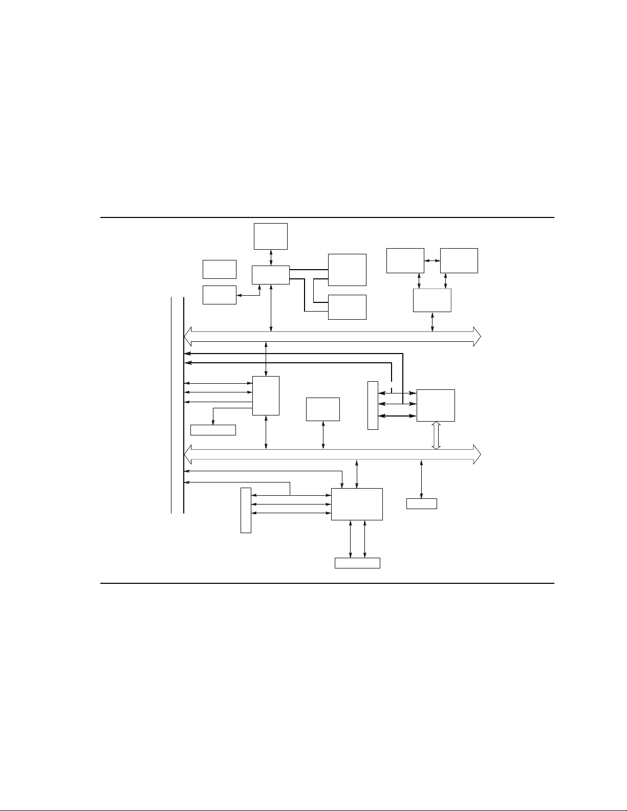
Processor
Socket
DC/DC
Converter
SDRAM
DIMM(3)
North Bridge
82440LX
A.G.P. Bus
A.G.P.
Connector
CL-GD5465
Graphics
Accelerator
Remote
Wakeup
Controller
82557
LAN
Controller
Intel
82555
Phy
Pri. IDE
Sec. IDE
USB Port 1
USB Port 0
Card Edge (for Riser)
Rear I/O Panel
Consumer IR or IrDA
PCI Bus
Rear I/O Panel
Keyboard
Mic In
Line Out
Line In
South
Bridge
(PIIX4)
Serial Port B
Serial Port A
Parallel Port
Rear I/O Panel
Floppy
LM78/79
Hardware
Monitor
ISA Bus
SMC
FDC37C677
I/O Controller
Mouse
Rear I/O Panel
Figure 1. Motherboard Block Diagram
OPL3-SA3
Audio
Controller
Flash
OM06480
8
Page 9
Motherboard Description
A
B
C
V
D
E
U
T
F
S
R
G
H
Q
P
I
J
K
O
N
LM
OM06250
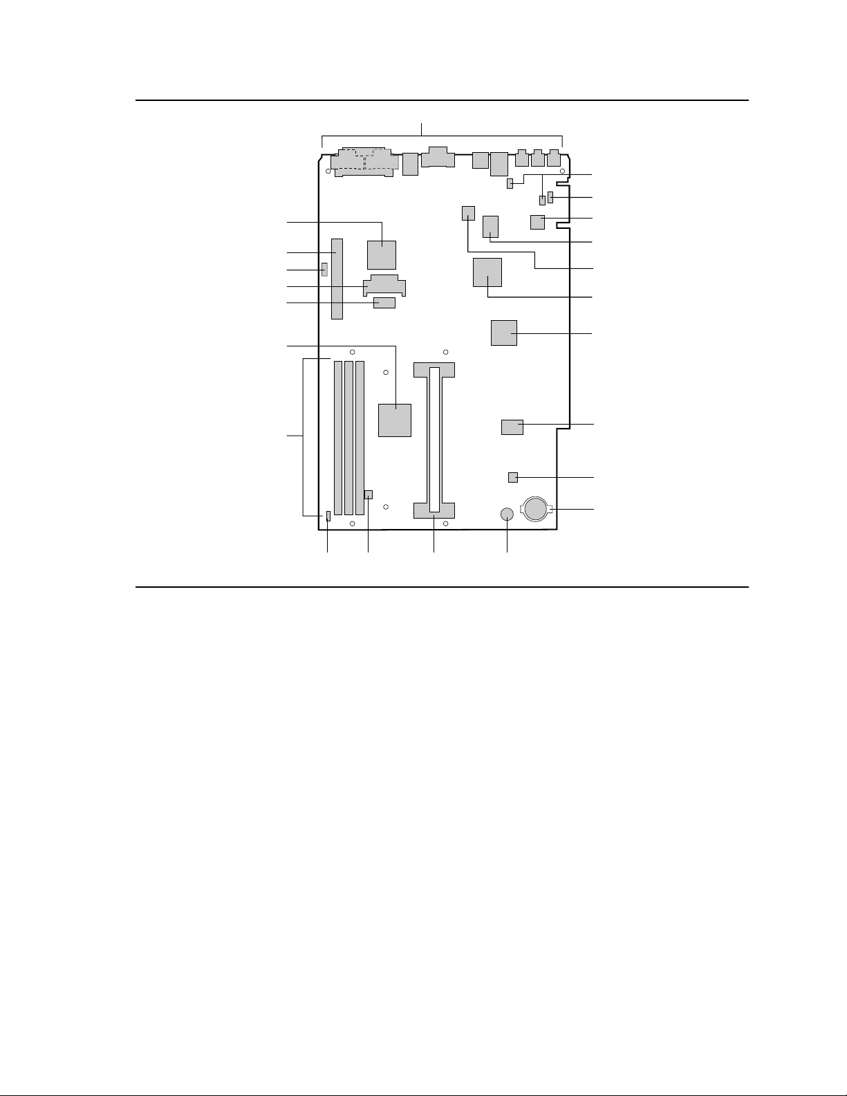
Figure 2. Motherboard Components
A Back panel connectors L Piezo speaker
B Yamaha wavetable headers M Slot 1 connector
C CD-ROM header N Fan connector
D Yamaha OPL3-SA3 (YMF715) O Configuration jumper
E Intel 82555 PHY P DIMM sockets
F Remote wakeup controller Q Intel 82443LX controller
G Intel 82557 LAN controller R Optional RAMBUS video memory
H Intel 82371AB PIIX4 S Optional RAMBUS memory upgrade socket
I SMC FDC37C677 T Onboard video configuration jumper
J National Semiconductor LM78/79 U A.G.P. connector
K Battery V Optional CL-GD5465 graphics accelerator
9
Page 10
NX440LX Motherboard Technical Product Specification
1.2 Form Factor
The motherboard is designed to fit into a standard NLX form factor chassis. Figure 3 illustrates the
mechanical form factor for the motherboard. Location of the I/O connectors, riser slot, and
mounting holes are in strict compliance with the NLX specification (see Section 6.2). Dimensions
are given in inches.
8.70
8.50
0.260
0.0
0.50
0.0
0.349
0.509
1.849
2.108
6.575
9.234
0.260
10
8.80
12.80
4.207.60
Figure 3. Motherboard Dimensions
13.00
0.20
OM06251
Page 11
Motherboard Description
1.3 I/O Shield
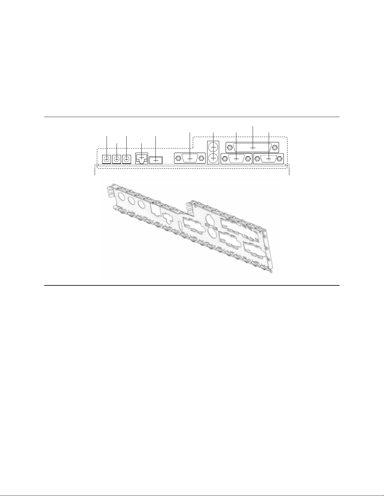
The back panel I/O shield for the NX440LX motherboard must meet specific dimensional and
material requirements. Systems based on this motherboard need the back panel I/O shield in order
to pass emission certification testing. Figure 4 shows the critical dimensions for both options of
the I/O shield, and indicates the position of each cutout. Dimensions are given in inches.
7.458
3.1461.6530.507
1.080
0.00 9.00
2.479
5.728
8.1826.7504.706
NLX Motherboard Shield
Figure 4. Back Panel I/O Shield Dimensions
OM06255
11
Page 12

NX440LX Motherboard Technical Product Specification
1.4 Microprocessor
The motherboard supports a single Pentium II processor. The processor’s VID pins automatically
program the motherboard’s voltage regulator to the required processor voltage. The motherboard
operates with processors that run internally at 233, 266, or 300 MHz and have either a 256 KB or
512 KB second-level cache.
The processor implements MMX technology and maintains full backward compatibility with the
8086, 80286, Intel386, Intel486, and Pentium processor. The processor’s numeric coprocessor
significantly increases the speed of floating-point operations and complies with ANSI/IEEE
standard 754-1985.
1.4.1 Microprocessor Packaging
The processor is packaged in a Single Edge Contact (S.E.C.) cartridge. The S.E.C. cartridge
includes the processor core, the second-level cache, a thermal plate, and a back cover.
The processor connects to the motherboard through the Slot 1 processor connector, a 242-pin edge
connector. When the processor is mounted in Slot 1, it is secured by a retention mechanism
attached to the motherboard. The processor’s heatsink is stabilized by a heatsink support that is
attached to the motherboard.
1.4.2 Second-Level Cache
The second-level cache is located on the substrate of the S.E.C. cartridge. The cache includes burst
pipelined synchronous static RAM (PBSRAM) and tag RAM. There can be two or four BSRAM
components totaling 256 KB or 512 KB in size. All supported onboard memory can be cached.
1.4.3 Microprocessor Upgrades
The motherboard can be upgraded with Pentium II processors that run at higher processor speeds.
After upgrading the processor, use the BIOS configuration mode to set the proper speed for the
processor. See Section 1.15.2 for information about configuration mode.
12
Page 13

Motherboard Description
1.5 Memory
1.5.1 Main Memory
The motherboard has three, dual inline memory module (DIMM) sockets. Minimum memory size
is 16 MB; maximum memory size is 384 MB. The BIOS automatically detects memory type, size,
and speed.
The motherboard supports the following memory features:
• 168-pin DIMMs with gold-plated contacts
• 66 MHz unbuffered SDRAM only
• Non-ECC (64-bit) and ECC (72-bit) memory
• 3.3 V memory only
• Single- or double-sided DIMMs in the following sizes:
DIMM Size Non-ECC Configuration ECC Configuration
16 MB 2 Mbit x 64 2 Mbit x 72
32 MB 4 Mbit x 64 4 Mbit x 72
64 MB 8 Mbit x 64 8 Mbit x 72
128 MB 16 Mbit x 64 16 Mbit x 72
Memory can be installed in one, two, or three sockets. Memory size can vary between sockets.
1.5.2 SDRAM
Synchronous DRAM (SDRAM) improves memory performance through memory access that is
synchronous with the memory clock. This simplifies the timing design and increases memory
speed because all timing is dependent on the number of memory clock cycles.
NOTE
✏
To function properly, SDRAM DIMMs must meet the Intel 4-clock, 66 MHz, unbuffered SDRAM
specification for either 64-bit or 72-bit SDRAM. See Section 6.2 for information about these
specifications.
13
Page 14

NX440LX Motherboard Technical Product Specification
1.5.3 ECC Memory
Error checking and correcting (ECC) memory detects multiple-bit errors and corrects single-bit
errors. When ECC memory is installed, the BIOS supports both ECC and non-ECC mode. ECC
mode is enabled in the Setup program. The BIOS automatically detects if ECC memory is
installed and provides the Setup option for selecting ECC mode. If non-ECC memory is installed,
the Setup option for ECC mode does not appear.
The following table describes the effect of using Setup to put each memory type in each supported
mode. Whenever ECC mode is selected in Setup, some performance loss occurs.
Memory Error Detection Mode Established in Setup Program
ECC Disabled ECC Enabled
Non-ECC DIMM
ECC DIMM
No error detection N/A
No error detection Single-bit error correction, multiple-bit error
detection
1.6 Chipset
The Intel 440LX is designed for the Pentium II processor. It consists of the Intel 82443LX
PCI/A.G.P. controller (PAC) and the Intel 82371AB PCI/ISA IDE Xcelerator (PIIX4) bridge chip.
1.6.1 Intel 82443LX PCI/A.G.P. Controller
The PAC provides bus-control signals, address paths, and data paths for transfers between the
processor’s host bus, PCI bus, Accelerated Graphics Port (A.G.P.), and main memory. The PAC
comes in a 492-pin BGA package and features:
• Processor interface control
Processor host bus speed up to 66 MHz
32-bit addressing
GTL+ compliant host bus
• Integrated DRAM controller
Supports synchronous DRAM (SDRAM)
64/72-bit path-to-memory
Auto detection of memory type
Supports 4-, 16-, 64-Mbit DRAM devices
Symmetrical and asymmetrical DRAM addressing
Supports 3.3 V DRAMs
• Accelerated Graphics Port Interface
Complies with A.G.P. specification (see Section 6.2 for specification information)
Supports 3.3 V A.G.P. devices with data transfer rates up to 133 MHz
Synchronous coupling to the host-bus frequency
14
Page 15

Motherboard Description
• Fully-synchronous PCI bus interface
Complies with PCI specification (see Section 6.2 for specification information)
PCI-to-DRAM access greater than 100 MB/sec
‡
Supports five
PCI bus masters in addition to the host and PCI-to-ISA I/O bridge
Delayed transactions
PCI parity generation and checking support
• Data Buffering
Host-to-DRAM, PCI-to-DRAM, and A.G.P.-to-DRAM write-data buffering
Write-combining for host-to-PCI burst writes
Supports concurrent host, PCI, and A.G.P. transactions to main memory
• Supports system management mode (SMM)
1.6.2 Intel 82371AB PCI ISA IDE Xcelerator (PIIX4)
The PIIX4 is a multifunction PCI device implementing the PCI-to-ISA bridge, PCI IDE
functionality, Universal Serial Bus (USB) host/hub function, and enhanced power management.
The PIIX4 comes in a 324-pin MBGA package that features:
• Multifunction PCI-to-ISA bridge
Supports the PCI bus at 33 MHz
Complies with PCI specification (see Section 6.2 for specification information)
Full ISA or extended I/O (EIO) bus support
• USB controller
‡
Two
Supports legacy keyboard and mouse
Supports UHCI design guide revision 1.1 interface
• Integrated dual-channel enhanced IDE interface
Supports up to four IDE devices
PIO Mode 4 transfers at up to 14 MB/sec
Supports Ultra DMA/33 synchronous DMA mode transfers up to 33 MB/sec
Bus master mode with an 8 x 32-bit buffer for bus master PCI IDE burst transfers
• Enhanced DMA controller
Two 8237-based DMA controllers
Supports PCI DMA with three PC/PCI channels and distributed DMA protocols
Fast type-F DMA for reduced PCI bus usage
• Interrupt controller based on 82C59
Supports 15 interrupts
Programmable for edge/level sensitivity
Supports serial IRQs
• Power management logic
Sleep/resume logic
Supports wake-on-modem through Ring Indicator input
Supports remote wakeup
USB ports (see Section 6.2 for compliance level).
15
Page 16

NX440LX Motherboard Technical Product Specification
• Real-Time Clock
256 byte battery-backed CMOS SRAM
Includes date alarm
• 16-bit counters/timers based on 82C54
1.6.3 Accelerated Graphics Port (A.G.P.)
The Accelerated Graphics Port (A.G.P.) is a high-performance interconnect for graphic-intensive
applications, such as 3D applications. A.G.P. is independent of the PCI bus and is intended for
exclusive use with graphical-display devices. A.G.P. provides these performance features:
• Pipelined-memory read and write operations that hide memory access latency
• Demultiplexing of address and data on the bus for near 100 percent bus efficiency
• AC timing for 133 MHz data transfer rates, allowing data throughput of 500 MB/sec
A.G.P. complies with the 66 MHz PCI specification. See Section 6.2 for information about the
A.G.P. and PCI specifications.
NOTE
✏
Due to the location of the third DIMM socket, only half-length AGP cards are supported.
1.6.3.1 CL-GD5465 High-performance Graphics Accelerator
The optional CL-GD5465 supports the A.G.P. for higher bandwidth between the system memory
and the graphics subsystem. It is a member of the Laguna family of RAMBUS-based graphics
accelerators, offering 3D-graphics capability while maintaining a high level of 2D performance.
The features include:
• 64-bit graphics engine with integrated 3D game acceleration
• High-performance 64-bit GUI accelerator
• Video playback acceleration
†
• Integrated VGA
• Integrated 230-MHz palette DAC and clock synthesizer
controller
16
Page 17

Motherboard Description
Table 1. Video Resolution
Resolution Supported No. of Colors
640 x 480, 800 x 600, 1024 x 768, 1280 x 1024, 1600 x 1200 256 (8 bit)
640 x 480, 800 x 600, 1024 x 768, 1280 x 1024 65,536 (16 bit)
640 x 480, 800 x 600, 1024 x 768 16,777,216 (24 bit)
640 x 480, 800 x 600, 1024 x 768, 1280 x 1024, 1600 x 1200 256 (8 bit)
640 x 480, 800 x 600, 1024 x 768, 1280 x 1024 65,536 (16 bit)
640 x 480, 800 x 600, 1024 x 768 16,777,216 (24 bit)
640 x 480, 800 x 600, 1024 x 768 16,777,216(32 bit)
640 x 480, 800 x 600, 1024 x 768, 1280 x 1024, 1600 x 1200 256 (8 bit)
640 x 480, 800 x 600, 1024 x 768, 1280 x 1024 65,536 (16 bit)
640 x 480, 800 x 600, 1024 x 768 16,777,216 (24 bit)
640 x 480, 800 x 600, 1024 x 768, 1280 x 1024 256 (8 bit)
640 x 480, 800 x 600, 1024 x 768 65,536 (16 bit)
1.6.4 Universal Serial Bus (USB)
The motherboard can support two‡ USB ports; however, it is shipped with only one connector.
The second is supported through the NLX riser. If you need to connect more than one USB device,
you can connect an external hub to the USB port. The motherboard fully supports the universal
host controller interface (UHCI) and uses UHCI-compatible software drivers. See Section 6.2 for
information about the USB specification. USB features include:
• Self-identifying peripherals that can be plugged in while the computer is running
• Automatic mapping of function to driver and configuration
• Supports isochronous and asynchronous transfer types over the same set of wires
• Supports up to 127 physical devices per USB port
• Bandwidth and low latencies appropriate for telephony, audio, and other applications
• Error-handling and fault-recovery mechanisms built into the protocol
NOTE
✏
Computer systems that have an unshielded cable attached to a USB port may not meet FCC
Class B or other regulatory EMI requirements, even if no device or a low-speed (sub-channel)
USB device is attached to the cable. Use shielded cable that meets the requirements for high-speed
(fully-rated) devices.
1.6.5 IDE Support
The motherboard has two independent bus-mastering capable PCI IDE interfaces. These interfaces
support PIO Mode 3, PIO Mode 4, ATAPI devices (e.g., CD-ROM), and Ultra DMA/33
synchronous-DMA mode transfers. The BIOS supports logical block addressing (LBA) and
extended cylinder head sector (ECHS) translation modes. The BIOS automatically detects the IDE
device transfer rate.
17
Page 18

NX440LX Motherboard Technical Product Specification
Programmed I/O operations usually require a substantial amount of processor bandwidth.
However, in multitasking operating systems, the bandwidth freed by bus mastering IDE can be
devoted to other tasks while disk transfers are occurring.
1.6.6 Real-Time Clock, CMOS SRAM, and Battery
The real-time clock is compatible with DS1287 and MC146818 components. The clock provides a
time-of-day clock and a multicentury calendar with alarm features and century rollover. The realtime clock supports 256 bytes of battery-backed CMOS SRAM in two banks that are reserved for
BIOS use.
The time, date, and CMOS values can be specified in the Setup program. The CMOS values can
be returned to their defaults by using the Setup program.
An external coin-cell battery powers the real-time clock and CMOS memory. When the computer
is not plugged into a wall socket, the battery has an estimated life of three years. When the
computer is plugged in, the 5 V standby current from the power supply extends the life of the
battery. The clock is accurate to ± 13 minutes/year at 25 ºC with 5 V applied.
1.7 I/O Interface Controller
• Enhanced Ultra I/O SMC FDC37C677
5 Volt operation
ISA Plug-and-Play compatible register set
• Two serial ports or one serial port and one infrared port
• One floppy controller
• FIFO support on both serial and floppy interfaces
• One parallel port with ECP and EPP support
†
• PS/2
• Supports BIOS setup for various configuration options
style mouse and keyboard interfaces
1.7.1 Serial Ports
The motherboard has two 9-pin D-Sub serial port connectors located on the back panel. The
NS16C550-compatible UARTs allow data transfers at speeds up to 115.2 Kbits/sec using BIOS
support.
1.7.2 Parallel Port
The connector for the multimode bi-directional parallel port is a 25-pin D-Sub connector located on
the back panel of the motherboard. In the Setup program, there are four options for parallel port
operation:
• Compatible (standard mode)
• Bi-directional (PS/2 compatible)
• Bi-directional Enhanced Parallel Port (EPP). A driver from the peripheral manufacturer is
required for operation. See Section 6.2 for EPP compatibility
• Bi-directional high-speed Extended Capabilities Port (ECP)
‡
18
Page 19

Motherboard Description
1.7.3 Floppy Controller
The I/O controller is software compatible with the 82077 floppy drive controller. The floppy
connector is located on the riser card. In the Setup program, the floppy interface can be configured
for the following floppy drive capacities and sizes:
• 1.2 MB, 5.25-inch
• 1.2 MB, 3.5-inch (Mode 3 floppy support, driver required)
• 1.44 MB, 3.5-inch
• 2.88 MB, 3.5-inch
• 120 MB (LS-120)
1.7.4 Keyboard and Mouse Interface
PS/2 keyboard and mouse connectors are located on the back panel of the motherboard. The +5 V
lines to these connectors are protected with a PolySwitch
reestablishes the connection after an over-current condition is removed. While this device
eliminates the possibility of having to replace a fuse, power to the computer should be turned off
before connecting or disconnecting a keyboard or mouse.
NOTE
✏
You can plug the mouse and keyboard into either connector.
The keyboard controller contains code which provides the traditional keyboard and mouse control
functions, and also supports Power On/Reset password protection. A Power On/Reset password
can be specified in the Setup program.
The keyboard controller supports the following hot-key sequence:
• <Ctrl><Alt><Del> Software reset. This key sequence resets the computer’s software by
jumping to the beginning of the BIOS code and running the Power-On Self Test (POST).
†
circuit that, like a self-healing fuse,
1.7.5 Optional Infrared
There is no infrared header on the motherboard; however, the edge connector does accommodate
infrared signals from the riser. If either IrDA
Configuration Submenu to change the mode for Serial Port B from COM2 to infrared applications.
†
or ASK-IR† is available, use the BIOS Peripheral
1.8 Audio Subsystem
1.8.1 OPL3-SA3 Audio System
The optional onboard audio subsystem features the Yamaha OPL3-SA3 (YMF715) device. The
features of the device include:
• A 16-bit audio codec
• OPL3 FM synthesis
• An integrated 3D enhanced stereo controller including all required analog components
• Stereo analog-to-digital and digital-to-analog converters
19
Page 20

NX440LX Motherboard Technical Product Specification
• Analog mixing, anti-aliasing, and reconstruction filters
• Supports 16-bit address decoding
• Line In, line out, and microphone connectors
• ADPCM, A-law, or µlaw digital audio compression and decompression
• Full digital control of all mixer and volume control functions
• Plug and Play compatible
†
• Sound Blaster Pro
NOTE
✏
Using the front panel line in, line out, and microphone connectors (if available on the riser)
disables the back panel connectors.
and Microsoft Windows Sound System compatible
20
Page 21

Motherboard Description
1.8.2 Audio Subsystem Resources
The following table shows the IRQ, DMA channel, and base I/O address options for the audio
subsystem. Options are listed in order of preference specified by Yamaha. These options are
automatically chosen by the Plug and Play interface, so there are no default settings. Onboard
audio can be enabled or disabled in the Setup program.
Table 2. Audio Subsystem Resources
IRQ
Resource
Sound Blaster
(DMA playback, DMA shared with
Windows Sound System capture)
Windows Sound System
(DMA playback)
MPU-401
(IRQ shared with Sound Blaster)
MIDI / Game Port 201h
†
AdLib
†
(Options)
10
7
5,7, 10,11
5
11
5,7, 10,11
DMA Channel
(Options)
1
0,1,3
0
0,1,3
I/O Address
(Options)
220-22Fh
240-24Fh
16 bytes on 16-byte
boundary in the
range of 220-280h
530-537h
E80-E87h
8 bytes on 8-byte
boundary in the
range of 530-F48h
330-331h
300-301h
2 bytes on 2-byte
boundary in the
range of 300-334h
1 byte on 1-byte
boundary in the
range of 201-20Fh
388-38Dh
6 bytes on 8-byte
boundary in the
range of 388-3F8h
1.8.3 Audio Drivers and Utilities
Audio software and utilities are available from Intel’s World Wide Web site (see Section 6.1).
Audio driver support is provided for the Microsoft Windows
†
Microsoft Windows NT
(versions 3.51 and 4.0), and IBM OS/2† Warp† (versions 3.0 and 4.0)
operating systems.
†
3.1, Microsoft Windows 95,
21
Page 22

NX440LX Motherboard Technical Product Specification
1.8.4 Audio Connectors
The audio connectors include the following connectors:
• Back panel connectors: Line In, Mic In, Line Out
• CD-ROM audio
• Hardware wavetable
1.8.4.1 CD-ROM Audio Connector
An optional 1 x 4-pin Creative Labs-type connector (J9N1) is available for connecting an internal
CD-ROM drive to the audio mixer. The connector is designed for audio add-in cards and is
compatible with most cables supplied with Creative Labs CD-ROM drives. Audio signals from the
riser are supported on the edge connector.
1.8.4.2 Hardware Wavetable Headers
Two 2 x 3-pin headers (J9M1, J7N1) are available for a wavetable add-in module. An optional
OPL4-ML reference design module that can be plugged into the motherboard may be licensed from
Yamaha Corporation. Compatible wavetable module cards are available from several vendors.
1.9 Hardware Monitor
The optional management extension hardware provides low-cost instrumentation capabilities on a
National Semiconductor LM78/79 chip. The features include:
• Integrated temperature sensor
• Fan speed sensors
• Power supply voltage monitoring to detect levels above or below acceptable values
• Remote reset capabilities from a remote peer or server through LANDesk
Version 3.0 and service layers
See Section 6.2 for information about the management extension hardware specification. For more
information, please check the following web site: http://www.national.com/pf/LM/
Client Manager,
1.10 Tamper Detection
If the riser is equipped with a tamper detection switch, the motherboard will emit a continuous
beep anytime the cover is opened and the A/C power cord is still connected. This warning is
intended to remind the user that 5 V standby power is still applied within the system. To avoid this
warning, unplug the power cord before opening the cover. The act of removing the cover will still
be recorded by circuitry on the motherboard, to be subsequently reported to any management suite
software in use.
CAUTION
Disconnecting the power cord can leave the system without an adequate electrical ground. Use
proper procedures to prevent electrostatic discharge (ESD) which could damage your system.
22
Page 23

Motherboard Description
1.11 Onboard Networking
The onboard networking subsystem is an Ethernet† LAN interface that provides both 10Base-T and
100Base-TX connectivity. Onboard LAN can be enabled or disabled in the Setup program.
Features include:
• 32-bit direct bus mastering on the PCI bus
• Shared memory structure in the host memory that copies data directly to/from host memory
• 10Base-T and 100Base-TX capability using a single RJ-45 connector
• IEEE 802.3µ Auto-Negotiation for the fastest available connection
• Jumperless configuration; the LAN subsystem is completely software configurable
• Remote wake up controller
1.11.1 Intel 82557 LAN Controller
This device is the heart of the LAN subsystem. It provides the following functions:
• CSMA/CD protocol engine
• PCI compatibility
• DMA engine for movement of commands, status, and network data across the PCI bus
• Standard MII interface for access to IEEE 802.3µ -compliant physical layer devices
1.11.2 Intel 82555 PHY 10 / 100 Mbit/sec Physical Layer Interface
The physical layer interface provides the following:
• Integrated 10/100 Mbit/sec single chip solution
• Complete 10/100 Mbit/sec media independent interface compliance with MDI support
• Full duplex operation available in both 10 and 100 Mbit/sec modes
• 25 MHz clock for 10 and 100 Mbit/sec modes
• Single magnetics module for 10 and 100 Mbit/sec operation
• IEEE 802.3µ Auto-Negotiation support for 10Base-T, 10Base-T FDX, 100Base-TX FDX,
100Base-TX FDX-FC
• Parallel detection algorithm for legacy support of non-Auto-Negotiation enabled link partner
• Glueless interface to TX solution with single magnetics module
• LED function mapping support via MDI interface
• Support for a LAN activity LED on an NLX riser
‡
1.11.3 Remote Wakeup Controller
The Remote Wakeup ASIC performs the Wake on LAN† function of the motherboard via the
onboard LAN interface. When the system is powered off, the Remote Wakeup ASIC and the
82555 PHY remain powered by a 5 V standby voltage. The ASIC monitors network traffic at the
MII interface and when it detects a Magic Packet
system.
†
it asserts a wakeup signal that powers up the
If an external network interface card (NIC) with remote wakeup capabilities is added to the
system
‡
the NIC’s remote wakeup header must be connected to the header on an NLX riser.
23
Page 24

NX440LX Motherboard Technical Product Specification
1.11.4 LAN Software
The software for the LAN subsystem, including setup/diagnostic software and a readme file viewer
that lists supported drivers, is available on the web site. See Section 6.1.
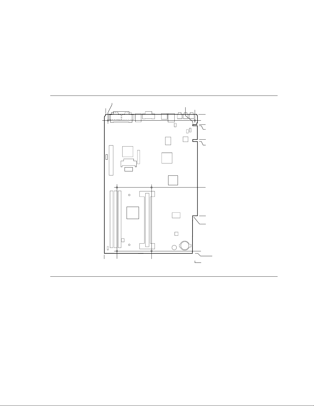
1.12 Motherboard Connectors
The following figure shows the connectors on the motherboard.
Onboard
Video
Configuration
Jumper
J1J1
A. G. P.
J1K1
DIMM Sockets(3)
J1D1, J2D1
J2D2
J7N1
1
5
Yamaha Wavetable
J9M1
2
1
J9N1
4
6
Creative
Labs
CD-ROM
Supplemental Gold Finger
Edge Connector
A-channel
RAMBUS
Memory
Interface
Riser Gold Finger
Edge Connector
4
1
24
Configuration
Jumper
J1A1
Fan
1
3
J2B1
Slot 1
Connector
J4D1
Figure 5. Motherboard Connectors
OM06256
Page 25

Motherboard Description
Table 3. CD Audio Connector (J9N1)
Pin Signal Name
1 Ground
2 CD_IN-Left
3 Ground
4 CD_IN-Right
Table 4. Accelerated Graphics Port (J1K1)
Pin Signal Name Pin Signal Name Pin Signal Name Pin Signal Name
A1 +12 V B1 No Connect A34 Vcc3.3 B34 Vcc3.3
A2 No Connect B2 Vcc A35 AGP_AD22 B35 AGP_AD21
A3 Reserved B3 Vcc A36 AGP_AD20 B36 AGP_AD19
A4 No Connect B4 No Connect A37 Ground B37 Ground
A5 Ground B5 Ground A38 AGP_AD18 B38 AGP_AD17
A6 PIRQ0# B6 PIRQ1# A39 AGP_AD16 B39 AGP_CBE2
A7 RST# B7 HCLK_AGP A40 Vcc3.3 B40 Vcc3.3
A8 AGP_GNT1# B8 AGP_REQ1 A41 AGP_FRAME# B41 AGP_IRDY#
A9 Vcc3.3 B9 Vcc3.3 A42 Reserved B42 Reserved
A10 AGP_ST1 B10 AGP_ST0 A43 Ground B43 Ground
A11 Reserved B11 AGP_ST2 A44 Reserved B44 Reserved
A12 AGP_PIPE# B12 AGP_DBF# A45 Vcc3.3 B45 Vcc3.3
A13 Ground B13 Ground A46 AGP_TRDY# B46 AGP_DEVSEL#
A14 No Connect B14 No Connect A47 AGP_STOP# B47 Vcc3.3
A15 SBA1 B15 SBA0 A48 PCI_PM* B48 AGP_PERR#
A16 Vcc3.3 B16 Vcc3.3 A49 Ground B49 Ground
A17 SBA3 B17 SBA2 A50 AGP_PAR B50 AGP_SERR#
A18 Reserved B18 SB_STB A51 AGP_AD15 B51 AGP_CBE1
A19 Ground B19 Ground A52 Vcc3.3 B52 Vcc3.3
A20 SBA5 B20 SBA4 A53 AGP_AD13 B53 AGP_AD14
A21 SBA7 B21 SBA6 A54 AGP_AD11 B54 AGP_AD12
A22 Key B22 Key A55 Ground B55 Ground
A23 Key B23 Key A56 AGP_AD9 B56 AGP_AD10
A24 Key B24 Key A57 AGP_CBE0 B57 AGP_AD8
A25 Key B25 Key A58 Vcc3.3 B58 Vcc3.3
A26 AGP_AD30 B26 AGP_AD31 A59 Reserved B59 AD_STBA
A27 AGP_AD28 B27 AGP_AD29 A60 AGP_AD6 B60 AGP_AD7
A28 Vcc3.3 B28 Vcc3.3 A61 Ground B61 Ground
A29 AGP_AD26 B29 AGP_AD27 A62 AGP_AD4 B62 AGP_AD5
A30 AGP_AD24 B30 AGP_AD25 A63 AGP_AD2 B63 AGP_AD3
A31 Ground B31 Ground A64 Vcc3.3 B64 Vcc3.3
A32 Reserved B32 AD_STBB A65 AGP_AD0 B65 AGP_AD1
A33 AGP_CBE3 B33 AGP_AD23 A66 SMDATA B66 SMBCLK
25
Page 26

NX440LX Motherboard Technical Product Specification
Table 5. Yamaha Wavetable Module
Connectors (J9M1) and
(J7N1)
Connector (J9M1)
Pin Signal Name
1 EXTEN#
2 SIN
3 Vcc
4 Ground
5 BCK
6 LACK
Connector (J7N1)
Pin Signal Name
1 RSTSLOT
2 Vcc
3 AUD33MHZ
4 MIDI Out
5 Ground
6 Key
Note: There are two 2x3 headers that connect to the
Yamaha wavetable daughter card
Table 6. Fan Header (J2B1)
Pin Signal Name
1 GND
2 Fan Power
3 Tachometer
26
Page 27

1.13 Back Panel Connectors
Motherboard Description
LineInLine
Mic
Out
In
Parallel Port
Mouse/
Keyboard
Serial Port 1Serial Port 2
(optional)
USBLAN
Figure 6. Back Panel I/O Connectors
Video
OM06254
27
Page 28

NX440LX Motherboard Technical Product Specification
1.14 Onboard Video Configuration Jumper Block
The following figure illustrates the onboard video configuration jumper at J1J1.
Onboard
Video
Configuration
J1J1
3
1
OM06521
Figure 7. Onboard Video Configuration Jumper Block
Table 7. Onboard Video Configuration Jumper Block (J1J1)
Function Jumper Configuration
Enable 1-2 Enables onboard video.
Disable 2-3 Disables onboard video and allows use of an add-in A.G.P. card or any video
on the riser.
NOTE
✏
Due to the location of the third DIMM socket, only half-length A.G.P. cards are supported.
28
Page 29

Motherboard Description
1.15 Configuration Jumper
The following figure shows the location of the configuration jumper block on the motherboard.
Configuration
Jumper
3
1
J1A1
OM06252
Figure 8. Single Configuration Jumper Block
Table 8. Configuration Jumper Table (J1A1)
Function Jumper Configuration
Normal 1-2 The BIOS uses current configuration information and passwords for booting.
Configure 2-3 After the POST runs, Setup is run automatically, using BIOS defaults. The
maintenance menu is displayed.
Recovery none The BIOS attempts to recover the BIOS configuration. A recovery diskette is
required.
CAUTION
Moving the jumper with the power on can damage your computer. Always turn off the power and
unplug the power cord from the computer before changing the jumper.
1.15.1 Normal Mode
This mode is for normal computer booting and operations. To enable this mode, pins 1 and 2 must
be connected on the configuration jumper (J1A1). The BIOS uses the current bus/processor
frequency ratio, configuration information, and passwords to boot the computer. Access to the
Setup program can be restricted using a supervisor or user password.
29
Page 30

NX440LX Motherboard Technical Product Specification
1.15.2 Configuration Mode
This mode is for configuring special BIOS settings, including processor speed and special
maintenance options. This mode is used when upgrading the BIOS, upgrading the processor, or
clearing the passwords. To enable this mode, pins 2 and 3 must be connected on the configuration
jumper (J1A1). In this mode, Setup automatically executes after the POST runs. No password is
required, and this mode overrides any passwords that are set. The Maintenance menu is the first
menu displayed. This menu provides options for setting the processor speed and clearing
passwords. All other Setup screens are available. Configure mode uses the default BIOS settings
for booting, not the current user or supervisor settings. The default settings include using the
lowest bus/processor frequency ratio the processor supports. User and supervisor settings are
preserved and used when the computer is rebooted.
For the configuration changes to take effect after exiting the Setup program, power down the
computer, set the configuration jumper to normal mode (see Section 1.15.1), and boot the
computer.
1.15.3 Recovery Mode
This mode is for recovering BIOS data. To enable this mode, no pins are connected on the
configuration jumper (J1A1). After the computer is powered-on, the BIOS attempts to upgrade or
recover the BIOS data from a floppy diskette in the floppy drive. If a diskette is not in the boot
drive, the BIOS runs the POST, does not boot the operating system, and displays a message that
the jumper is not properly installed. If the recovery fails with a diskette in the boot drive, a beep
code indicates that the recovery failed.
For the configuration changes to take effect after a successful recovery, power down the computer,
set the configuration jumper to normal mode (see Section 1.15.1), and boot the computer.
30
Page 31

Motherboard Description
1.16 NLX Card Edge Connector
The NLX riser connector on the motherboard consists of a 340 (2x170) position and a
supplemental 26 (2x13) position gold finger contact. All edge connector pin definitions are
defined in the NLX specification, version 1.2.
According to the NLX specification, the motherboard edge connector provides the following:
• PCI signals (the motherboard supports up to four PCI devices)
• ISA signals
• 2 IDE channels
• 1 floppy drive
• Infrared signals
• Miscellaneous front panel signals
• Power connection for the motherboard
See Section 6.2 for information about the NLX Specification.
Table 9, Table 10, and Table 11 specify the pinouts located on the primary connector; Table 12
specifies the pinouts located on the supplemental connector. All edge connector pin definitions are
defined in the NLX specification, version 1.2.
Table 9. PCI Segment, Riser Interconnect Pin-out
Pin# Signal Name Type I/O Termination Pin Signal Name Type I/O Termination
A1 -12V PWR NA NA B1 PCSPKR_RT AUDIO O NA
A2 REQ4# PCI I RIS B2 +12V PWR NA NA
A3 +12V PWR NA NA B3 PCSPKR_LFT AUDIO O NA
A4 GNT4# PCI O RIS B4 +12V PWR NA NA
A5 3.3VDC PWR NA NA B5 PCICLK0 PCI O MB
A6 PCIINT3# PCI I RIS B6 GND PWR NA NA
A7 3.3VDC PWR NA NA B7 PCICLK1 PCI O MB
A8 PCIINT0# PCI I RIS B8 SER_IRQ MISC I/O MB
A9 PCIINT1# PCI I RIS B9 PCIINT2# PCI I RIS
A10 PCICLK2 PCI O MB B10 3.3VDC PWR NA NA
A11 3.3VDC PWR NA NA B11 PCICLK3 PCI O MB
A12 PCI_RST# PCI O MB B12 GND PWR NA NA
A13 GNT0# PCI O RIS B13 GNT3# PCI O RIS
A14 PCICLK4 PCI O MB B14 3.3VDC PWR NA NA
A15 GND PWR NA NA B15 GNT2# PCI O RIS
A16 GNT1# PCI O RIS B16 AD[31] PCI I/O RIS
continued
☛
31
Page 32

NX440LX Motherboard Technical Product Specification
Table 9. PCI Segment, Riser Interconnect Pin-out
(continued)
Pin# Signal Name Type I/O Termination Pin Signal Name Type I/O Termination
A17 3.3VDC PWR NA NA B17 REQ0# PCI I RIS
A18 REQ2# PCI I RIS B18 GND PWR NA NA
A19 REQ3# PCI I RIS B19 AD[29] PCI I/O RIS
A20 AD[30] PCI I/O RIS B20 AD[28] PCI I/O RIS
A21 GND PWR NA NA B21 AD[26] PCI I/O RIS
A22 AD[25] PCI I/O RIS B22 3.3VDC PWR NA NA
A23 REQ1# PCI I RIS B23 AD[24] PCI I/O RIS
A24 AD[27] PCI I/O RIS B24 C/BE[3]# PCI I/O RIS
A25 3.3VDC PWR NA NA B25 AD[22] PCI I/O RIS
A26 AD[23] PCI I/O RIS B26 GND PWR NA NA
A27 AD[20] PCI I/O RIS B27 AD[21] PCI I/O RIS
A28 AD[18] PCI I/O RIS B28 AD[19] PCI I/O RIS
A29 GND PWR NA NA B29 AD[16] PCI I/O RIS
A30 AD[17] PCI I/O RIS B30 3.3VDC PWR NA NA
A31 IRDY# PCI I/O RIS B31 C/BE[2]# PCI I/O RIS
A32 DEVSEL# PCI I/O RIS B32 FRAME# PCI I/O RIS
A33 3.3VDC PWR NA NA B33 TRDY# PCI I/O RIS
A34 STOP# PCI I/O RIS B34 GND PWR NA NA
A35 PERR# PCI I/O RIS B35 SDONE PCI I/O RIS
A36 SERR# PCI I/O RIS B36 LOCK# PCI I/O RIS
A37 GND PWR NA NA B37 SBO# PCI I/O RIS
A38 C/BE[1]# PCI I/O RIS B38 3.3VDC PWR NA NA
A39 AD[13] PCI` I/O RIS B39 AD[15] PCI I/O RIS
A40 AD[10] PCI I/O RIS B40 PAR PCI I/O RIS
A41 GND PWR NA NA B41 AD[14] PCI I/O RIS
A42 C/BE[0]# PCI I/O RIS B42 GND PWR NA NA
A43 AD[00] PCI I/O RIS B43 AD[11] PCI I/O RIS
A44 AD[06] PCI I/O RIS B44 AD[12] PCI I/O RIS
A45 3.3VDC PWR NA NA B45 AD[09] PCI I/O RIS
A46 AD[05] PCI I/O RIS B46 3.3VDC PWR NA NA
A47 AD[01] PCI I/O RIS B47 AD[08] PCI I/O RIS
A48 AD[03] PCI I/O RIS B48 AD[07] PCI I/O RIS
A49 GND PWR NA NA B49 AD[04] PCI I/O RIS
A50 AD[02] PCI I/O RIS B50 GND PWR NA NA
A51 5VDC PWR NA NA B51 PCI_PM# PCI I/O MB
I/O Column Definitions Relative to Motherboard
O = Output from motherboard to riser
I = Input from riser to motherboard
Termination Column Definitions:
MB = Termination/Pullup/Pulldown/debounce is on Motherboard
RIS = Termination/Pullup/Pulldown is on Riser card
N/A = Not on Motherboard or Riser
32
Page 33

Motherboard Description
Table 10. ISA Segment, Riser Interconnect Pin-out
Pin Signal Name Type I/O Termination Pin Signal Name Type I/O Termination
A52 RSTDRV ISA O MB B52 5VDC PWR NA NA
A53 IOCHK# ISA I MB B53 IRQ9 ISA O MB
A54 SD[6] ISA I/O MB B54 DRQ2 ISA I MB
A55 SD[7] ISA I/O MB B55 SD[3] ISA I/O MB
A56 SD[4] ISA I/O MB B56 0WS# ISA I MB
A57 5VDC PWR NA NA B57 SD[1] ISA I/O MB
A58 SD[2] ISA I/O MB B58 AEN ISA O MB
A59 SD[5] ISA I/O MB B59 IOCHRDY ISA I MB
A60 SD[0] ISA I/O MB B60 SA[18] ISA I/O MB
A61 SMEMW# ISA O MB B61 SMEMR# ISA O MB
A62 SA[19] ISA I/O MB B62 SA[16] ISA I/O MB
A63 IOW# ISA I/O MB B63 IOR# ISA I/O MB
A64 SA[17] ISA I/O MB B64 DRQ3 ISA I MB
A65 GND PWR NA NA B65 SA[15] ISA I/O MB
A66 DACK#3 ISA O MB B66 GND PWR NA NA
A67 SA[14] ISA I/O MB B67 SA[13] ISA I/O MB
A68 DACK1# ISA O MB B68 5VDC PWR NA NA
A69 DRQ1 ISA I MB B69 REFRESH# ISA I/O MB
A70 SA[12] ISA I/O MB B70 SA[11] ISA I/O MB
A71 SYSCLK ISA O MB B71 SA[10] ISA I/O MB
A72 SA[9] ISA I/O MB B72 IRQ7 ISA I MB
A73 5VDC PWR NA NA B73 IRQ6 ISA I MB
A74 IRQ5 ISA I MB B74 SA[8] ISA I/O MB
A75 SA[7] ISA I/O MB B75 SA[6] ISA I/O MB
A76 IRQ3 ISA I MB B76 DACK2# ISA O MB
A77 IRQ4 ISA I MB B77 SA[4] ISA I/O MB
A78 SA[5] ISA I/O MB B78 GND PWR NA NA
A79 TC ISA O MB B79 SA[3] ISA I/O MB
A80 BALE ISA O MB B80 SA[2] ISA I/O MB
A81 GND PWR NA NA B81 SA[1] ISA I/O MB
A82 OSC ISA O MB B82 SA[0] ISA I/O MB
A83 IOCS16# ISA I MB B83 SBHE# ISA I/O MB
continued ☛
33
Page 34

NX440LX Motherboard Technical Product Specification
Table 10. ISA Segment, Riser Interconnect Pin-out
(continued)
Pin Signal Name Type I/O Termination Pin Signal Name Type I/O Termination
A84 MEMCS16# ISA I MB B84 LA[23] ISA I/O MB
A85 IRQ11 ISA I MB B85 LA[22] ISA I/O MB
A86 IRQ10 ISA I MB B86 LA[21] ISA I/O MB
A87 IRQ15 ISA I MB B87 LA[20] ISA I/O MB
A88 IRQ12 ISA I MB B88 LA[19] ISA I/O MB
A89 GND PWR NA NA B89 LA[18] ISA I/O MB
A90 IRQ14 ISA I MB B90 LA[17] ISA I/O MB
A91 DRQ0 ISA I MB B91 DACK0# ISA O MB
A92 MEMR# ISA I/O MB B92 DACK5# ISA O MB
A93 MEMW# ISA I/O MB B93 SD[8] ISA I/O MB
A94 SD[9] ISA I/O MB B94 DACK6# ISA O MB
A95 DRQ5 ISA I MB B95 SD[10] ISA I/O MB
A96 DRQ6 ISA I MB B96 5VDC PWR NA NA
A97 5VDC PWR NA NA B97 SD[11] ISA I/O MB
A98 SD[12] ISA I/O MB B98 DRQ7 ISA I MB
A99 DACK7# ISA O MB B99 SD[13] ISA I/O MB
A100 SD[14] ISA I/O MB B100 SD[15] ISA I/O MB
A101 MASTER# ISA I MB B101 GND PWR NA NA
I/O Column Definitions Relative to Motherboard
O = Output from motherboard to riser
I = Input from riser to motherboard
Termination Column Definitions:
MB = Termination/Pullup/Pulldown/debounce is on Motherboard
RIS = Termination/Pullup/Pulldown is on Riser card
N/A = Not on Motherboard or Riser
Table 11. IDE, Floppy, and Front Panel Section, Riser Interconnect Pin-out
Pin Signal Name Type I/O Termination Pin Signal Name Type I/O Termination
A102 IDEA_DD8 IDE I/O MB B102 GND PWR NA NA
A103 IDEA_RESET# IDE O MB B103 IDEA_DD7 IDE I/O MB
A104 IDEA_DD9 IDE I/O MB B104 IDEA_DD6 IDE I/O MB
A105 5VDC PWR NA NA B105 IDEA_DD5 IDE I/O MB
A106 IDEA_DD4 IDE I/O MB B106 IDEA_DD11 IDE I/O MB
A107 IDEA_DD10 IDE I/O MB B107 IDEA_DD12 IDE I/O MB
A108 IDEA_DD3 IDE I/O MB B108 GND PWR NA NA
A109 IDEA_DD13 IDE I/O MB B109 IDEA_DD14 IDE I/O MB
A110 IDEA_DD1 IDE I/O MB B110 IDEA_DD2 IDE I/O MB
A111 GND PWR NA NA B111 IDEA_DD0 IDE I/O MB
A112 IDEA_DIOW# IDE O MB B112 IDEA_DD15 IDE I/O MB
continued
☛
34
Page 35

Motherboard Description
Table 11. IDE, Floppy, and Front Panel Section, Riser Interconnect Pin-out
(continued)
Pin Signal Name Type I/O Termination Pin Signal Name Type I/O Termination
A113 IDEA_DMARQ IDE I MB B113 IDEA_DIOR# IDE O MB
A114 IDEA_IORDY IDE I MB B114 IDEA_CSEL IDE O MB
A115 IDEA_DMACK# IDE O MB B115 IDEA_INTRQ IDE I MB
A116 RESERVED RES NA NA B116 5VDC PWR NA NA
A117 IDEA_DA2 IDE O MB B117 IDEA_DA1 IDE O MB
A118 IDEA_CS0# IDE O MB B118 IDEA_DA0 IDE O MB
A119 5VDC PWR NA NA B119 IDEA_CS1# IDE O MB
A120 IDEA_DASP# IDE I RIS B120 IDEB_DD8 IDE I/O MB
A121 IDEB_RESET# IDE O MB B121 IDEB_DD7 IDE I/O MB
A122 IDEB_DD9 IDE I/O MB B122 GND PWR NA NA
A123 IDEB_DD6 IDE I/O MB B123 IDEB_DD10 IDE I/O MB
A124 IDEB_DD5 IDE I/O MB B124 5VDC PWR NA NA
A125 IDEB_DD11 IDE I/O MB B125 IDEB_DD4 IDE I/O MB
A126 IDEB_DD12 IDE I/O MB B126 IDEB_DD3 IDE I/O MB
A127 GND PWR NA NA B127 IDEB_DD13 IDE I/O MB
A128 IDEB_DD2 IDE I/O MB B128 IDEB_DD14 IDE I/O MB
A129 IDEB_DD15 IDE I/O MB B129 IDEB_DD1 IDE I/O MB
A130 IDEB_DIOW# IDE I/O MB B130 IDEB_DD0 IDE I/O MB
A131 IDEB_DMARQ IDE I MB B131 IDEB_DIOR# IDE O MB
A132 IDEB_IORDY IDE I MB B132 IDEB_CSEL IDE O MB
A133 GND PWR NA NA B133 IDEB_INTRQ IDE I MB
A134 IDEB_DMACK# IDE O MB B134 IDEB_DA1 IDE O MB
A135 RESERVED RES NA NA B135 IDEB_DA2 IDE O MB
A136 IDEB_DA0 IDE O MB B136 IDEB_CS1# IDE O MB
A137 IDEB_CS0# IDE O MB B137 IDEB_DASP# IDE I RIS
A138 DRV2# FLOPPY GND NA B138 GND PWR NA NA
A139 5VDC PWR NA NA B139 DRATE0 FLOPPY O NA
A140 RESERVED RES NA NA B140 FDS1# FLOPPY O NA
A141 DENSEL FLOPPY O NA B141 FDS0# FLOPPY O NA
A142 FDME0# FLOPPY O NA B142 DIR# FLOPPY O NA
A143 INDX# FLOPPY I RIS B143 MSEN1 FLOPPY I NA
continued
☛
35
Page 36

NX440LX Motherboard Technical Product Specification
Table 11. IDE, Floppy, and Front Panel Section, Riser Interconnect Pin-out
(continued)
Pin Signal Name Type I/O Termination Pin Signal Name Type I/O Termination
A144 FDME1# FLOPPY O NA B144 GND PWR NA NA
A145 GND PWR NA NA B145 WRDATA# FLOPPY O NA
A146 WE# FLOPPY O NA B146 TRK0# FLOPPY I RIS
A147 STEP# FLOPPY O NA B147 MSEN0 FLOPPY I NA
A148 WP# FLOPPY I RIS B148 RDDATA# FLOPPY I RIS
A149 HDSEL# FLOPPY O NA B149 DSKCHG# FLOPPY I RIS
A150 SDA MISC I/O MB B150 GND PWR NA NA
A151 SCL MISC O MB B151 IRSL0 MISC I/O NA
A152 FAN_TACH1 MISC I NA B152 IRSL1 MISC I/O NA
A153 FAN_TACH2 MISC I NA B153 IRSL2 MISC I/O NA
A154 FAN_TACH3 MISC I NA B154 IRTX MISC I/O NA
A155 FAN_CTL MISC I NA B155 IRRX MISC I/O NA
A156 5VDC PWR NA NA B156 FP_SLEEP MISC I MB
A157 USB1/3_N MISC I/O RIS B157 FP_RST# MISC I MB
A158 USB1/3_P MISC I/O RIS B158 GND PWR NA NA
A159 USB1/3_OC# MISC I RIS B159 PWRLED# MISC O RIS
A160 USB2/4_N MISC I/O RIS B160 PWOK PWR I NA
A161 USB2/4_P MISC I/O RIS B161
A162 USB2/4_OC# MISC I RIS B162 PS_ON# PWR O NA
A163 GND PWR NA NA B163 LAN_WAKE MISC I MB
A164 VBAT MISC O RIS B164 LAN_ACTVY_
A165 TAMP_DET# MISC I MB B165 MDM_WAKE# MISC I MB
A166 MSG_WAIT_
LED#
A167 1394_GND PWR O NA B167 RESERVED RES NA NA
A168 RESERVED RES NA NA B168 RESERVED RES NA NA
A169 5VSB PWR I NA B169 RESERVED RES NA NA
A170 3.3VSENSE PWR O NA B170 -5V PWR NA NA
I/O Column Definitions Relative to Motherboard
O = Output from motherboard to riser
I = Input from riser to motherboard
Termination Column Definitions:
MB = Termination/Pullup/Pulldown/debounce is on Motherboard
RIS = Termination/Pullup/Pulldown is on Riser card
N/A = Not on Motherboard or Riser
MISC O RIS B166 1394_PWR PWR I NA
SOFT_ON/OFF#
LED#
PWR I MB
MISC O NA
36
Page 37

Motherboard Description
Table 12. Signals, NLX Riser with Supplemental Connector
Pin Signal Name Type I/O * Description Signal Type
X1 CD_IN_LT AUDIO I CD-ROM line in left. Analog
1 V RMS
X2 AGND PWR NA Low pass filtered ground for audio circuitry on
the riser.
X3 MIC_IN AUDIO I Pre-amplified microphone input. Pre-amp
circuitry to reside on riser or in microphone.
X4 LINE_OUT_LT AUDIO O Analog line out left. Analog
X5 FP_SPKR_EN ** AUDIO I This signal indicates if headphones have
been plugged into the front panel LINE OUT
jack. The signal is connected to one of the
wipers on the audio jack and is HIGH when
the headphones are plugged into the front
audio jack and LOW when they are not. The
signal is pulled high through a pull-up on the
motherboard (Typically 100K).
X6 VOL_DN# ** AUDIO I Connects to Volume Down switch on front
panel, appropriate pull-up resistor on
motherboard. The motherboard provides
debounce protection and a pull-up resistor.
X7 GND PWR NA Ground NA
X8 SMI# ** SYS I System Management Interrupt that is an
input to the motherboard.
X9 RESERVED RES NA Reserved NA
X10 RESERVED RES NA Reserved NA
X11 RESERVED RES NA Reserved NA
X12 AGND PWR NA Low pass filtered ground for audio circuitry on
the riser.
X13 MODEM_MIC AUDIO O Pre-amplified microphone mono output signal
from motherboard to telephony device.
CD_IN_RT AUDIO I CD-ROM line in right. Analog
Y1
CD_IN_GND PWR I Isolated CD-ROM Ground. NA
Y2
AVCC PWR O Clean power from the motherboard to audio
Y3
circuitry on the NLX riser; could be an
isolated power source; 1.5 Ampere max.
limitation because of the connector / gold
finger limitation.
LINE_OUT_RT AUDIO O Analog line out right. Analog
Y4
NA
Analog
1 V RMS
1 V RMS
TTL
TTL
open drain
NA
Analog
1 V RMS
1 V RMS
5-9 V DC
1 V RMS
continued ☛
37
Page 38

NX440LX Motherboard Technical Product Specification
Table 12. Signals, NLX Riser with Supplemental Connector
Pin Signal Name Type I/O * Description Signal Type
Y5 FP_MIC_EN ** AUDIO I This signal indicates if a microphone has
been plugged into the front panel MIC_IN
jack. The signal is connected to a wiper on
the MIC_IN jack and is LOW when the
microphone is plugged in and HIGH when it
is not. The signal is pulled LOW through a
pull down on the motherboard (Typically
100K).
Y6 VOL_UP# ** AUDIO I Connects to Volume Up switch on front
panel, appropriate pull-up resistor on
motherboard. The motherboard provides
debounce protection and a pull-up resistor.
Y7 AC_RST# ** AC’97 O AC’97 master H/W reset. TTL
Y8 AC_SD_IN ** AC’97 I Serial, time division, multiplexed, AC’97 input
stream to the motherboard from the codec
on the riser (output from the codec).
Y9 GROUND PWR NA Digital (main motherboard) ground plane. NA
Y10 AC_SD_OUT ** AC’97 O Serial, time division, multiplexed, AC’97
output from the motherboard to the codec on
the riser (input to the codec).
Y11 AC_SYNC ** AC’97 O 48KHz fixed rate sample sync signal from
the motherboard to the codec on the riser.
Y12 AC_BIT_CLK ** AC’97 I 12.288 MHz serial data clock. TTL
Y13 MODEM_SPKR AUDIO O Analog mono output signal from telephony
device to motherboard.
* I/O column: relative to motherboard, “O” = output, from motherboard to riser; “I” = input, from riser to motherboard.
** These signals are not supported.
(continued)
TTL
TTL
TTL
TTL
TTL
Analog
1V RMS
1.17 Reliability
The Mean Time Between Failures (MTBF) data is calculated from predicted data at 55 ºC.
Motherboard MTBF: 186,417 hours
38
Page 39

1.18 Environmental
Table 13. Motherboard Environmental Specifications
Parameter Specification
Temperature
Non-Operating
Operating
Shock
Unpackaged 50 G trapezoidal waveform
Packaged Half sine 2 millisecond
Vibration
Unpackaged 5 Hz to 20 Hz : 0.01g² Hz sloping up to 0.02 g² Hz
Packaged 10 Hz to 40 Hz : 0.015g² Hz (flat)
-40 °C to +70 °C
0 °C to +55 °C
Velocity change of 170 inches/second
Product Weight Free Fall (inches) Velocity Change (inches/sec)
<20 lbs. 36 167
21-40 lbs. 30 152
41-80 lbs. 24 136
81-100 lbs. 18 118
20 Hz to 500 Hz : 0.02g² Hz (flat)
40 Hz to 500 Hz : 0.015g² Hz sloping down to 0.00015 g² Hz
Motherboard Description
39
Page 40

NX440LX Motherboard Technical Product Specification
1.19 Power Consumption
Tables 14 and 15 list voltage and current specifications for a computer that contains the
motherboard, a 266 MHz Pentium II processor, 16 MB RAM, 512 KB cache, 3.5-inch floppy
drive, 2.1 GB IDE hard drive, and a 8X IDE CD-ROM drive. This information is provided only as
a guide for calculating approximate power usage with additional resources added.
Values for the Windows 95 desktop mode are measured at 640 x 480 x 256 colors and 60 Hz
refresh rate. AC watts are measured with a typical 145 W supply, nominal input voltage and
frequency, with true RMS wattmeter at the line input.
Table 14. DC Voltage
DC Voltage Acceptable Tolerance
+3.3 V ± 4%
+5 V ± 5%
+5 V SB (standby) ± 5%
-5 V ± 5%
+12 V ± 5%
-12 V ± 5%
Table 15. Power Usage
DC (amps) at:
Mode AC (watts) +3.3 V +5 V -5 V +12 V -12 V
DOS prompt, APM disabled 63 1.2 A 4.5 A 0.1 A 0.7 A 0.2 A
Windows 95 desktop, APM disabled 64 1.0 A 5.3 A 0.1 A 0.6 A 0.2 A
Windows 95 desktop, APM enabled, in
System Management Mode (SMM)
30 1.0 A 1.0 A 0.1 A 0.2 A 0.2 A
For typical configurations, the motherboard is designed to operate with at least a 200 W NLX
power supply (see Section 6.2 for the specification). Use a higher wattage supply for heavily
loaded configurations. The power supply must comply with the NLX power supply
recommendations.
40
Page 41

Motherboard Description
1.20 Regulatory Compliance
This printed circuit assembly complies with the following safety and EMI regulations when
correctly installed in a compatible host system.
1.20.1 Safety
1.20.1.1 UL 1950 - CSA 950-95, 3rd edition, Dated 07-28-95
The Standard for Safety of Information Technology Equipment including Electrical Business
Equipment. (USA & Canada)
1.20.1.2 CSA C22.2 No. 950-93, 3rd Edition
The Standard for Safety of Information Technology Equipment including Electrical Business
Equipment. (Canada)
1.20.1.3 EN 60 950, 2nd Edition, 1992 (with Amendments 1, 2 & 3)
The Standard for Safety of Information Technology Equipment including Electrical Business
Equipment. (European Union)
1.20.1.4 IEC 950, 2nd edition, 1991 (with Amendments 1, 2 & 3)
The Standard for Safety of Information Technology Equipment including Electrical Business
Equipment. (International)
1.20.1.5 EMKO-TSE (74-SEC) 207/94
Summary of Nordic deviations to EN 60 950. (Norway, Sweden, Denmark & Finland)
1.20.2 EMI
1.20.2.1 FCC Class B
Title 47 of the Code of Federal Regulations, Parts 2 & 15, Subpart B, pertaining to unintentional
radiators. (USA)
1.20.2.2 CISPR 22, 2nd Edition, 1993
Limits and methods of measurement of Radio Interference Characteristics of Information
Technology Equipment. (International)
1.20.2.3 EN 55 022, 1995
Limits and methods of measurement of Radio Interference Characteristics of Information
Technology Equipment. (Europe)
41
Page 42

NX440LX Motherboard Technical Product Specification
1.20.2.4 EN 50 082-1 (1992)
Generic Immunity Standard; Currently compliance is determined via testing to IEC 801-2, -3,
and -4. (Europe)
1.20.2.5 VCCI Class 2 (ITE)
Implementation Regulations for Voluntary Control of Radio Interference by Data Processing
Equipment and Electronic Office Machines. (Japan)
1.20.2.6 ICES-003, Issue 2
Interference-Causing Equipment Standard, Digital Apparatus. (Canada)
1.20.3 Product Certification Markings
This printed circuit assembly has the following product certification markings:
• European CE Marking: Consists of a marking on the board and shipping container.
• UL Recognition Mark: Consists of the UL File No. E139761 on the component side of the
board and the PB No. on the solder side of the board. Board material flammability is
94V-1 or -0.
• Canadian Compliance: Consists of small c followed by a stylized backward UR on component
side of board.
42
Page 43

2 Motherboard Resources
NOTE
✏
For more detailed information about the resources used for onboard audio, see the Audio
Subsystem section in Chapter 1.
2.1 Memory Map
Table 16. Memory Map
Address Range (decimal) Address Range (hex) Size Description
1024 K - 393216 K 100000 - 18000000 383 MB Extended memory
1008 K - 1024 K FC000 - FFFFF 16 KB Boot block
1000 K - 1008 K FA000 - FBFFF 8 KB ESCD (Plug and Play configuration and
DMI)
996 K - 1000 K F9000 - F9FFF 4 KB Reserved for BIOS
992 K - 996 K F8000 - F8FFF 4 KB OEM Logo or Scan User Flash
928 K - 992 K E8000 - F7FFF 64 KB POST BIOS
896 K - 928 K E0000 - E7FFF 32 KB POST BIOS (Available as UMB)
800 K - 896 K C8000 - DFFFF 96 KB Available high DOS memory (open to ISA
and PCI bus)
640 K - 800 K A0000 - C7FFF 160 KB Video memory and BIOS
639 K - 640 K 9FC00 - 9FFFF 1 KB Extended BIOS data (movable by memory
manager software)
512 K - 639 K 80000 - 9FBFF 127 KB Extended conventional memory
0 K - 512 K 00000 - 7FFFF 512 KB Conventional memory
2.2 DMA Channels
Table 17. DMA Channels
DMA Channel Number Data Width System Resource
0 8- or 16-bits Audio
1 8- or 16-bits Audio / Parallel Port
2 8- or 16-bits Floppy Drive
3 8- or 16-bits Parallel Port (for ECP or EPP) / Audio
4 Reserved - Cascade Channel
5 16-bits Open
6 16-bits Open
7 16-bits Open
43
Page 44

NX440LX Motherboard Technical Product Specification
2.3 I/O Map
Table 18. I/O Map
Address (hex) Size Description
0000 - 000F 16 bytes PIIX4- DMA 1
0020 - 0021 2 bytes PIIX4 - interrupt controller 1
002E - 002F 2 bytes I/O controller configuration registers
0040 - 0043 4 bytes PIIX4 - Counter/Timer 1
0048 - 004B 4 bytes PIIX4- Counter/Timer 2
0060 1 byte Keyboard Controller Byte - Reset IRQ
0061 1 byte PIIX4 - NMI, Speaker Control
0064 1 byte Keyboard controller, CMD/STAT Byte
0070, bit 7 1 bit PIIX4 - enable NMI
0070, bits 6:0 7 bits PIIX4 - real time clock, address
0071 1 byte PIIX4 - real time clock, data
0078 1 byte Reserved - motherboard configuration
0079 1 byte Reserved - motherboard configuration
0080 - 008F 16 bytes PIIX4 - DMA page registers
00A0 - 00A1 2 bytes PIIX4 - interrupt controller 2
00B2 - 00B3 2 bytes APM control
00C0 - 00DE 31 bytes PIIX4 - DMA 2
00F0 1 byte Reset numeric error
0170 - 0177 8 bytes Secondary IDE channel
01F0 - 01F7 8 bytes Primary IDE channel
0200 - 0207 8 bytes Audio / game port
0220 - 022F 16 bytes Audio (Sound Blaster compatible)
0240 - 024F 16 bytes Audio (Sound Blaster compatible)
0278 - 027F 8 bytes LPT2
0290 - 0297 8 bytes Management extension hardware
02E8 - 02EF 8 bytes COM4/Video (8514A)
02F8 - 02FF 8 bytes COM2
0300 - 0301 2 bytes MPU-401 (MIDI)
0330 - 0331 2 bytes MPU-401 (MIDI)
0332 - 0333 2 bytes MPU-401 (MIDI)
0334 - 0335 2 bytes MPU-401 (MIDI)
0376 1 byte Secondary IDE channel command port
0377 1 byte Floppy channel 2 command
0377, bit 7 1 bit Floppy disk change, channel 2
44
continued ☛
Page 45

Motherboard Resources
Table 18. I/O Map
Address (hex) Size Description
0377, bits 6:0 7 bits Secondary IDE channel status port
0378 - 037F 8 bytes LPT1
0388- 038D 6 bytes AdLib (FM synthesizer)
03B4 - 03B5 2 bytes Video (VGA)
03BA 1 byte Video (VGA)
03BC - 03BF 4 bytes LPT3
03C0 - 03CA 11 bytes Video (VGA)
03CC 1 byte Video (VGA)
03CE - 03CF 2 bytes Video (VGA)
03D4 - 03D5 2 bytes Video (VGA)
03DA 1 byte Video (VGA)
03E8 - 03EF 8 bytes COM3
03F0 - 03F5 6 bytes Floppy Channel 1
03F6 1 byte Primary IDE channel command port
03F7 (Write) 1 byte Floppy channel 1 command
03F7, bit 7 1 bit Floppy disk change channel 1
03F7, bits 6:0 7 bits Primary IDE channel status port
03F8 - 03FF 8 bytes COM1
04D0 - 04D1 2 bytes Edge/level triggered PIC
0530 - 0537 8 bytes Windows Sound System
0604 - 060B 8 bytes Windows Sound System
LPTn + 400h 8 bytes ECP port, LPTn base address + 400h
0CF8 - 0CFB* 4 bytes PCI configuration address register
0CF9** 1 byte Turbo and reset control register
0CFC - 0CFF 4 bytes PCI configuration data register
0E80 - 0E87 8 bytes Windows Sound System
0F40- 0F47 8 bytes Windows Sound System
0F86 - 0F87 2 bytes Yamaha OPL3-SA3 configuration
FF00 - FF07 8 bytes IDE bus master register
FFA0 - FFA7 8 bytes Primary bus master IDE registers
FFA8 - FFAF 8 bytes Secondary bus master IDE registers
(continued)
* DWORD access only
** Byte access only
NOTE
✏
See the Audio section(s) in Chapter 1 for specific I/O addresses that can be used by the audio
components on your motherboard. This table does not list I/O addresses that may be used by
add-in cards in the system.
45
Page 46

NX440LX Motherboard Technical Product Specification
2.4 PCI Configuration Space Map
Table 19. PCI Configuration Space Map
Bus
Number (hex)
00 00 00 Intel 82440LX (PAC)
00 01 00 Intel 82371AB (PIIX4 ) A.G.P. bus
00 07 00 Intel 82371AB (PIIX4 ) PCI/ISA bridge
00 07 01 Intel 82371AB (PIIX4 ) IDE bus master
00 07 02 Intel 82371AB (PIIX4 ) USB
00 07 03 Intel 82371AB (PIIX4 ) power management
00 14 00 PCI expansion slot 1
00 12 00 PCI expansion slot 2
00 06 00 Intel 82557 PCI Ethernet Controller (LAN)
01 00 00 Cirrus Logic CL-GD5465 A.G.P. Controller (Video)
2.5 Interrupts
Table 20. Interrupts
IRQ System Resource
NMI I/O Channel Check
0 Reserved, Interval Timer
1 Reserved, Keyboard Buffer Full
2 Reserved, Cascade Interrupt From Slave PIC
3 COM2*
4 COM1*
5 LPT2 (Plug and Play option) / Audio / User available
6 Floppy Drive
7 LPT1*
8 Real Time Clock
9 User available
10 User available
11 Windows Sound System* / User available
12 Onboard Mouse Port (if present, else user available)
13 Reserved, Math Coprocessor
14 Primary IDE (if present, else user available)
15 Secondary IDE (if present, else user available)
Device
Number (hex)
Function
Number (hex) Description
‡
‡
* Default, but can be changed to another IRQ
46
Page 47

2.6 PCI Interrupt Routing Map
Motherboard Resources
This section describes interrupt sharing and how the interrupt signals are connected between the
‡
PCI expansion slots
and onboard PCI devices. The PCI specification specifies how interrupts can
be shared between devices attached to the PCI bus. In most cases, the small amount of latency
added by interrupt sharing does not affect the operation or throughput of the devices. In some
special cases where maximum performance is needed from a device, a PCI device should not share
an interrupt with other PCI devices. Use the following information to avoid sharing an interrupt
with a PCI add-in card.
PCI devices are categorized as follows to specify their interrupt grouping:
• INTA: By default, all add-in cards that require only one interrupt are in this category. For
almost all cards that require more than one interrupt, the first interrupt on the card is also
classified as INTA.
• INTB: Generally, the second interrupt on add-in cards that require two or more interrupts is
classified as INTB. (This is not an absolute requirement.)
• INTC and INTD: Generally, a third interrupt on add-in cards is classified as INTC and a
fourth interrupt is classified as INTD.
The PIIX4 PCI-to-ISA bridge has four programmable interrupt request (PIRQ) input signals. Any
PCI interrupt source (either onboard or from a PCI add-in card) connects to one of these PIRQ
signals. Because there are only four signals, some PCI interrupt sources are mechanically tied
together on the motherboard and therefore share the same interrupt. Table 21 lists the PIRQ
‡
signals and shows how the signals are connected to the PCI expansion slots
and to onboard PCI
interrupt sources.
Table 21. PCI Interrupt Routing Map
PIIX4 PIRQ
Signal
PIRQA INTA INTD INTC
PIRQB INTB INTA INTD INTA
PIRQC INTC INTB INTA INTB INTA
PIRQD INTD INTC INTB INTA
First PCI
Expansion Slot
Second PCI
‡
Expansion Slot
Third PCI
‡
Expansion Slot
Onboard
‡
Video USB
Ethernet LAN
Controller
For example, assume an add-in card has one interrupt (group INTD) into the second PCI slot. In
this slot, an interrupt source from group INTA connects to the PIRQD signal, which is already
connected to the onboard video and USB PCI sources. The add-in card shares an interrupt with
these onboard interrupt sources.
Now, however, plug an add-in card that has one interrupt (group INTA) into the first PCI slot.
Plug a second add-in card that has two interrupts (groups INTA and INTB) into the second PCI
slot. INTA in the first slot is connected to signal PIRQA. INTA in the second slot is connected to
signal PIRQB, and INTB is connected to signal PIRQC. With no other cards added, the three
interrupt sources on the first two cards each have a PIRQ signal to themselves. Typically, they will
not share an interrupt.
47
Page 48

NX440LX Motherboard Technical Product Specification
NOTE
✏
The PIIX4 can connect each PIRQ line internally to one of the IRQ signals (3, 4, 5, 7, 9, 11, 14,
15). Typically, a device that does not share a PIRQ line will have a unique interrupt. However, in
certain interrupt-constrained situations, it is possible for two or more of the PIRQ lines to be
connected to the same IRQ signal.
48
Page 49

3 Overview of BIOS Features
The motherboard uses an Intel/Phoenix BIOS, which is stored in flash memory and can be
upgraded using a disk-based program. In addition to the BIOS, the flash memory contains the
Setup program, Power-On Self Test (POST), Advanced Power Management (APM) software, the
PCI auto-configuration utility, and Windows 95-ready Plug and Play. See Section 6.2 for the
supported versions of these specifications.
This motherboard supports system BIOS shadowing, allowing the BIOS to execute from 64-bit
onboard write-protected DRAM.
The BIOS displays a message during POST identifying the type of BIOS and a the revision code.
The initial production BIOS is identified as 4N4XL0X0.86A.
3.1 BIOS Upgrades
A new version of the BIOS can be upgraded from a diskette using the iFLASH.EXE utility that is
available from Intel. This utility does BIOS upgrades as follows:
• Updates the flash BIOS from a file on a disk
• Updates the language section of the BIOS
• Makes sure that the upgrade BIOS matches the target system to prevent accidentally installing
a BIOS for a different type of system.
BIOS upgrades and the iFLASH.EXE utility are available from Intel through the Intel World Wide
Web site. See Section 6.1 for information about this site.
NOTE
✏
Please review the instructions distributed with the upgrade utility before attempting a BIOS
upgrade.
49
Page 50

NX440LX Motherboard Technical Product Specification
3.2 BIOS Flash Memory Organization
The 2-Mbit flash component is organized as 256 KB x 8 bits and is divided into areas as described
in Table 22. The table shows the addresses in the ROM image in normal mode (the addresses
change in BIOS Recovery Mode).
Table 22. Flash Memory Organization
Address (Hex) Size Description
FFFFC000 - FFFFFFFF 16 KB Boot Block
FFFFA000 - FFFFBFFF 8 KB Vital Product Data (VPD) Extended System Configuration Data
(ESCD) (DMI configuration data / Plug and Play data)
FFFF9000 - FFFF9FFF 4 KB Used by BIOS (e.g., for Event Logging)
FFFF8000 - FFFF8FFF 4 KB OEM logo or Scan Flash Area
FFFC0000 - FFFF7FFF 224 KB Main BIOS Block
3.3 Plug and Play: PCI Autoconfiguration
The BIOS automatically configures PCI devices and Plug and Play devices. PCI devices may be
onboard or add-in cards. Plug and Play devices are ISA add-in cards built to meet the Plug and
Play specification. Autoconfiguration lets a user insert or remove PCI or Plug and Play cards
without having to configure the system. When a user turns on the system after adding a PCI or
Plug and Play card, the BIOS automatically configures interrupts, the I/O space, and other system
resources. Any interrupts set to Available in Setup are considered to be available for use by the
add-in card.
PCI interrupts are distributed to available ISA interrupts that have not been assigned to an ISA card
or to system resources. The assignment of PCI interrupts to ISA IRQs is non-deterministic. PCI
devices can share an interrupt, but an ISA device cannot share an interrupt allocated to PCI or to
another ISA device. Autoconfiguration information is stored in the extended system configuration
data (ESCD) format.
For information about the versions of PCI and Plug and Play supported by this BIOS, see
Section 6.2. Copies of the specifications can be obtained from the Intel World Wide Web site (see
Section 6.1).
50
Page 51

Overview of BIOS Features
3.4 PCI IDE Support
If Auto is selected as a primary or secondary IDE device (see Section 4.2.2) in Setup, the BIOS
automatically sets up the two local-bus IDE connectors with independent I/O channel support. The
IDE interface supports hard drives up to PIO Mode 4 and recognizes any ATAPI devices, including
CD-ROM drives and tape drives (see Section 6.2 for the supported version of ATAPI). The BIOS
determines the capabilities of each drive and configures them so as to optimize capacity and
performance. To take advantage of the high-capacity storage devices, hard drives are automatically
configured for logical block addressing (LBA) and to PIO Mode 3 or 4, depending on the
capability of the drive. To override the autoconfiguration options, use the specific IDE device
options in Setup. The ATAPI specification recommends that ATAPI devices be configured as
shown in Table 23.
Table 23. Recommendations for Configuring an ATAPI Device
Primary Cable Secondary Cable
Configuration
Normal, no ATAPI ATA
Disk and CD-ROM for enhanced IDE systems ATA ATAPI
Legacy IDE system with only one cable ATA ATAPI
Enhanced IDE with CD-ROM and a tape or two CD-ROMs ATA ATAPI ATAPI
Drive 0 Drive 1 Drive 0 Drive 1
3.5 ISA Plug and Play
If Plug and Play operating system (see Section 4.3) is selected in Setup, the BIOS autoconfigures
only ISA Plug and Play cards that are required for booting (IPL devices). If Plug and Play
operating system is not selected in Setup, the BIOS autoconfigures all Plug and Play ISA cards.
3.6 ISA Legacy Devices
Since ISA legacy devices are not autoconfigurable, the resources for them must be reserved.
Resources can be reserved in the Setup program.
51
Page 52

NX440LX Motherboard Technical Product Specification
3.7 Desktop Management Interface (DMI)
Desktop Management Interface (DMI) is an interface for managing computers in an enterprise
environment. The main component of DMI is the management information format (MIF) database,
which contains information about the computing system and its components. Using DMI, a system
administrator can obtain the system types, capabilities, operational status, and installation dates for
system components. The MIF database defines the data and provides the method for accessing this
information. The BIOS enables applications such as Intel LANDesk Client Manager to use DMI.
The BIOS stores and reports the following DMI information:
• BIOS data, such as the BIOS revision level
• Fixed-system data, such as peripherals, serial numbers, and asset tags
• Resource data, such as memory size, cache size, and processor speed
• Dynamic data, such as event detection and error logging
OEMs can use a utility that programs flash memory so the BIOS can report on system and chassis
information. This utility is available through Intel sales offices. See Section 6.1 for information
about contacting a local Intel sales office. See Section 6.2 for information about the latest DMI
specification.
DMI does not work directly under non-Plug and Play operating systems (e.g., Windows NT).
However, the BIOS supports a DMI table interface for such operating systems. Using this support,
a DMI service-level application running on a non-Plug and Play OS can access the DMI BIOS
information.
3.8 Advanced Power Management (APM)
The BIOS supports APM and standby mode. See Section 6.2 for the version of the APM
specification that is supported. The energy saving standby mode can be initiated in the following
ways:
• Time-out period specified in Setup
• Suspend/resume switch connected to the front panel sleep connector
• From the operating system, such as the Suspend menu item in Windows 95
In standby mode, the motherboard reduces power consumption by using SMM capabilities,
spinning down hard drives, and reducing power to or turning off VESA
monitors. Power-management mode can be enabled or disabled in Setup (see Section 4.5).
While in standby mode, the system retains the ability to respond to external interrupts and service
requests, such as incoming faxes or network messages. Any keyboard or mouse activity brings the
system out of standby mode and immediately restores power to the monitor.
The BIOS enables APM by default; but the operating system must support an APM driver for the
power-management features to work. For example, Windows 95 supports the power-management
features upon detecting that APM is enabled in the BIOS.
†
DPMS-compliant
52
Page 53

Overview of BIOS Features
3.9 Language Support
Five languages will be available: American English, German, Italian, French, and Spanish. The
BIOS includes extensions to support the Kanji character set and other non-ASCII character sets.
Translations of other languages may become available at a later date.
The default language is American English, which is always present unless another language is
programmed into the BIOS using the flash memory update utility. See Section 3.1 for information
about the BIOS update utility.
3.10 Boot Options
In the Setup program, the user can choose to boot from a floppy drive, hard drive, CD-ROM, or the
network. The default setting is for the floppy drive to be the primary boot device and the hard
drive to be the secondary boot device. By default the third and fourth devices are disabled.
Booting from CD-ROM is supported in compliance to the El Torito bootable CD-ROM format
specification. See Section 6.2 for information about the El Torito specification. Under the Boot
menu in the Setup program, CD-ROM is listed as a boot device. Boot devices are defined in
priority order. If the CD-ROM is selected as the boot device, it must be the first device.
The network can be selected as a boot device. This selection allows booting from a network add-in
card with a remote boot ROM installed.
3.11 OEM Logo or Scan Area
A 4 KB flash-memory user area at memory location FFFF8000h-FFFF8FFFh is for displaying a
custom OEM logo during POST. A utility is available from the Intel web site (see Section 6.1) to
assist with installing a logo into the flash memory. Contact Intel customer support for further
information. See Section 6.1 for information on contacting Intel customer support.
3.12 USB Support
The USB connectors allow any of several USB devices to be attached to the computer. Typically,
the device driver for USB devices is managed by the operating system. However, because
keyboard and mouse support may be needed in the Setup program before the operating system
boots, the BIOS supports USB keyboards and mice.
3.13 BIOS Setup Access
Access to the Setup program can be restricted using passwords. User and supervisor passwords
can be set using the Security menu in Setup. The default is no passwords enabled. See Section 4.4
for information about setting user and supervisor passwords.
53
Page 54

NX440LX Motherboard Technical Product Specification
3.14 Recovering BIOS Data
Some types of failure can destroy the BIOS. For example, the data can be lost if a power outage
occurs while the BIOS is being updated in flash memory. The BIOS can be recovered from a
diskette using the BIOS recovery mode (see Section 1.15.3).
To create a BIOS recovery diskette, a bootable diskette must be created and the recovery files
copied to it. The recovery files are available from Intel, contact Intel customer support for further
information. See Section 6.1 for information on contacting Intel customer support.
54
Page 55

4 BIOS Setup Program
The Setup program is for viewing and changing the BIOS settings for a computer. Setup is
accessed by pressing the <F2> key after the Power-On Self Test (POST) memory test begins and
before the operating system boot begins. Table 24 shows the menus available from the menu bar at
the top of the Setup screen.
Table 24. Setup Menu Bar
Setup Menu Screen Description
Maintenance Sets the processor speed and clears the Setup passwords.
Main Allocates resources for hardware components.
Advanced Sets advance features available through the chipset.
Security Sets passwords and security features.
Power Sets power management features.
Boot Sets boot options and power supply controls.
Exit Saves or discards changes.
Table 25 shows the function keys available for menu screens.
Table 25. Setup Function Keys
Setup Key Description
<F1> or <Alt-H> Brings up a help screen for the current item.
<Esc> Exits the menu.
<←> or <→>
<↑> or <↓>
<Home> or <End> Moves cursor to top or bottom of the window.
<PgUp> or <PgDn> Moves cursor to top or bottom of the window.
<F5> or <-> Selects the previous value for a field.
<F6> or <+> or <Space> Selects the next value for a field.
<F9> Load the default configuration values for the current menu.
<F10> Save the current values and exit Setup.
<Enter> Executes command or selects the submenu.
< + > and < - > Moves a device up and down the boot order list.
Selects a different menu screen.
Moves cursor up or down.
55
Page 56

NX440LX Motherboard Technical Product Specification
4.1 Maintenance Menu
This menu is for setting the processor speed and clearing the Setup passwords. Setup only displays
this menu in configure mode. See Section 1.15.2 for information about setting configure mode.
Table 26. Maintenance Menu
Feature Options Description
Processor Speed
Clear All Passwords None Clears the user and supervisor passwords.
• 233
• 266
• 300
Specifies the processor speed in megahertz.
4.2 Main Menu
This menu reports processor and memory information, and is for configuring the language, system
date, system time, floppy options, and IDE devices.
Table 27. Main Menu
Feature Options Description
Processor Type None Displays processor type.
Processor Speed None Displays processor speed.
Cache RAM None Displays size of L2 cache.
Total Memory None Displays the total amount of RAM on the motherboard.
BIOS Version None Displays the version of the BIOS.
Language
System Time Hour, minute,
System Date Month, day, and
Floppy Options,
submenu
Primary IDE Master,
submenu
Primary IDE Slave,
submenu
Secondary IDE
Master, submenu
Secondary IDE
Slave, submenu
• English (US)
(default)
• Italiana
• Français
• Deutsche
• Español
and second
year
None Configures the diskette drives. When selected, displays the
None Reports type of a connected IDE device. When selected, displays
None Reports type of a connected IDE device. When selected, displays
None Reports type of a connected IDE device. When selected, displays
None Reports type of a connected IDE device. When selected, displays
Selects the current default language used by the BIOS.
Specifies the current time.
Specifies the current date.
Floppy Options submenu. See Section 4.2.1.
the Primary IDE Master submenu. See Section 4.2.2.
the Primary IDE Slave submenu. See Section 4.2.2.
the Secondary IDE Master submenu. See Section 4.2.2.
the Secondary IDE Slave submenu. See Section 4.2.2.
56
Page 57

4.2.1 Floppy Options Submenu
This submenu is for configuring floppy drives.
Table 28. Floppy Options Submenu
Feature Options Description
Diskette A:
Diskette B:
Floppy Write Protect
• Disabled
• 360 KB, 5.25 inch
• 1.2 MB, 5.25 inch
• 720 KB, 3.5 inch
• 1.44/1.25 MB, 3.5 inch
(default)
• 2.88 MB, 3.5 inch
• Disabled (default)
• 360 KB, 5.25 inch
• 1.2 MB, 5.25 inch
• 720 KB, 3.5 inch
• 1.44/1.25 MB, 3.5 inch
• 2.88 MB, 3.5 inch
• Disabled (default)
• Enabled
BIOS Setup Program
Specifies the capacity and physical size
of the diskette drive A.
Specifies the capacity and physical size
of the diskette drive B.
Disables or enables write protect for the
diskette drive(s).
57
Page 58

NX440LX Motherboard Technical Product Specification
4.2.2 IDE Device Configuration Submenus
This submenu is for configuring the IDE device features for the following:
• Primary IDE master
• Primary IDE slave
• Secondary IDE master
• Secondary IDE slave
Table 29. IDE Device Configuration Submenus
Feature Options Description
Type
Cylinders 1 to
Heads 1 to 16 Specifies number of disk heads.
Sectors 1 to 64 Specifies number of disk sectors.
Maximum Capacity None Reports maximum capacity for the hard disk.
Multi-Sector Transfers
LBA Mode Control
None
•
ATAPI Removable
•
CD-ROM
•
IDE Removable
•
User
•
Auto (default)
•
XXXX
Disabled
•
2 Sectors
•
4 Sectors
•
8 Sectors
•
16 Sectors (default)
•
Disabled
•
Enabled (default)
•
Specifies the IDE configuration mode for IDE
devices.
User allows the cylinders, heads, and sectors
fields to be changed.
Auto automatically fills in the values for the
cylinders, heads, and sectors fields.
Specifies number of disk cylinders.
Value calculated from number of cylinders, heads,
and sectors.
Specifies number of sectors per block for
transfers from the hard drive to memory.
Check the hard drive’s specifications for optimum
setting of this feature.
Enables or disables logical block addressing (LBA)
in place of the Cylinders, Heads, and Sectors
fields.
58
32 Bit I/O
Transfer Mode
Ultra DMA
Disabled (default)
•
Enabled
•
Standard
•
Fast PIO 1
•
Fast PIO 2
•
Fast PIO 3
•
Fast PIO 4 (default)
•
Disabled (default)
•
Mode 0
•
Mode 1
•
Mode 2
•
CAUTION
Changing the LBA Mode Control after a
hard drive was formatted can corrupt data
on the hard drive.
Enables or disables 32 bit IDE data transfers
between the processor and the IDE device.
Specifies method for transferring data between
the hard drive and system memory.
Specifies the ultra DMA mode for the hard drive.
Page 59

4.3 Advanced Menu
This menu is for setting advance features that are available through the computer’s chipset.
Table 30. Advanced Menu
Feature Options Description
Plug & Play O/S
Reset Configuration Data
Memory Cache
Resource Configuration,
submenu
Peripheral Configuration,
submenu
Keyboard Features,
submenu
Video Configuration,
submenu
DMI Event Logging,
submenu
• No
• Yes (default)
• No (default)
• Yes
• Disabled
• Enabled (default)
None Configures memory blocks and IRQs for legacy ISA
None Configures peripheral ports and devices. When
None Configures keyboard features. When selected,
None Configures video features. When selected,
None Configures DMI Events Logging. When selected,
Specifies if a Plug and Play operating system is being
used.
No lets BIOS configure all devices.
Yes lets the operating system configure Plug and
Play devices. Not required with a Plug and Play
operating system.
Clears the BIOS configuration data on the next boot.
Enables or disables the memory cache.
devices. When selected, displays the Resource
Configuration submenu. See Section 4.3.1.
selected, displays the Peripheral Configuration
submenu. See Section 4.3.2.
displays the Keyboard Features submenu. See
Section 4.3.3.
displays the Video Configuration submenu.
See Section 4.3.4.
displays the DMI Events Logging submenu. See
Section 4.3.5.
BIOS Setup Program
59
Page 60

NX440LX Motherboard Technical Product Specification
4.3.1 Resource Configuration Submenu
This submenu is for configuring the memory and interrupts.
Table 31. Resource Configuration Submenu
Feature Options Description
Memory
Reservation
ECC
Configuration
IRQ
Reservation
• C800 - CBFF Available (default) | Reserved
• CC00- CFFF Available (default) | Reserved
• D000 - D3FF Available (default) | Reserved
• D400 - D7FF Available (default) | Reserved
• D800 - DBFF Available (default) | Reserved
• DC00 - DFFF Available (default) | Reserved
Memory hole Disabled (default) | Conventional | Extended
• Non-ECC (default)
• ECC
• IRQ3 Available (default) | Reserved
• IRQ4 Available (default) | Reserved
• IRQ5 Available (default) | Reserved
• IRQ7 Available (default) | Reserved
• IRQ9 Available (default) | Reserved
• IRQ10 Available (default) | Reserved
• IRQ11 Available (default) | Reserved
• IRQ15 Available (default) | Reserved
An * (asterisk) next to an IRQ indicates an IRQ conflict.
Reserves specific
upper memory blocks
for use by legacy ISA
devices.
Indicates if ECC
memory is present.
Reserves specific
IRQs for use by
legacy ISA devices.
60
Page 61

4.3.2 Peripheral Configuration Submenu
This submenu is for the configuring the computer peripherals.
Table 32. Peripheral Configuration Submenu
Feature Options Description
Serial Port A
Serial Port B
Mode
Parallel Port
Mode
Floppy Disk
Controller
IDE Controller
Audio
LAN
Legacy USB
Support
• Disabled
• Enabled
• Auto (default)
• Disabled
• Enabled
• Auto (default)
• Normal (default)
• IrDA
• ASK-IR
• Disabled
• Enabled
• Auto (default)
• Output Only
• Bi-directional (default)
• EPP
• ECP
• Disabled
• Enabled (default)
• Disabled
• Primary
• Secondary
• Both (default) (primary
and secondary)
• Disabled
• Enabled (default)
• Disabled
• Enabled (default)
• Disabled (default)
• Enabled
Used to configure serial port A.
Auto assigns the first free COM port, normally COM1,
the address 3F8h and the interrupt IRQ4.
An * (asterisk) indicates a conflict with another device.
Used to configure serial port B.
Auto assigns the first free COM port, normally COM2,
the address 2F8h and the interrupt IRQ3.
An * (asterisk) indicates a conflict with another device.
If either serial port address is set, that address will not
appear in the list of options for the other serial port.
If an ATI mach32
active as an add-in card, the COM4, 2E8h address will
not appear in the list of options for either serial port.
Sets the mode for Serial Port B for normal (COM2) or
infrared applications.
Configures the parallel port.
Auto assigns LPT1 the address 378h and the interrupt
IRQ7.
An * (asterisk) indicates a conflict with another device.
Selects the mode for the parallel port.
Output Only operates in AT
Bi-directional operates in bi-directional PS/2-compatible
mode.
EPP is Extended Parallel Port mode, a high-speed bi-
directional mode.
ECP is Enhanced Capabilities Port mode, a high-speed
bi-directional mode.
Configures the floppy disk controller.
Configures the IDE controller.
Enables or disables the onboard audio subsystem.
Enables or disables the onboard LAN subsystem.
Enables or disables BIOS support for USB keyboards
and mice.
BIOS Setup Program
†
or an ATI mach64† video controller is
†
-compatible mode.
61
Page 62

NX440LX Motherboard Technical Product Specification
4.3.3 Keyboard Configuration Submenu
Table 33. Keyboard Configuration Submenu
Feature Options Description
Numlock
Key Click
Keyboard Auto-repeat Rate
Keyboard Auto-repeat Delay
• Auto (default)
• On
• Off
• Disabled (default)
• Enabled
• 30/sec (default)
• 26.7/sec
• 21.8/sec
• 18.5/sec
• 13.3/sec
• 10/sec
• 6/sec
• 2/sec
• ¼ sec
• ½ sec (default)
• ¾ sec
• 1 sec
Sets the power on state of the Numlock feature
on the numeric keypad of the keyboard.
Enables the key click option.
Selects the key repeat rate.
Selects the delay before key repeat.
4.3.4 Video Configuration Submenu
Table 34. Video Configuration Submenu
Feature Options Description
Palette Snooping
• Disabled (default)
• Enabled
4.3.5 DMI Event Logging Submenu
Table 35. DMI Event Logging Submenu
Feature Options Description
Event Log Capacity None Indicates if there is space available in the event log.
Event Log Validity None Indicates if the contents of the event log are valid.
View DMI Event Log None Enables viewing of DMI event log.
Clear All DMI Event Logs
Event Logging
ECC Event Logging
Mark DMI Events as read None Marks all DMI events as read.
• No (default)
• Yes
• Disabled
• Enabled (default)
• Disabled (default)
• Enabled
Controls the ability of a primary PCI graphics
controller to share a common palette with an ISA
add-in video card.
Clears the DMI Event Log after rebooting.
Enables logging of DMI events.
62
Page 63

4.4 Security Menu
This menu is for setting passwords and security features for the computer.
Table 36. Security Menu
Feature Options Description
User Password Is None Reports if there is a user password set.
Supervisor Password Is None Reports if there is a supervisor
Set User Password Password can be up to seven
alphanumeric characters.
Set Supervisor Password Password can be up to seven
alphanumeric characters.
Unattended Start
• Disabled (default)
• Enabled
BIOS Setup Program
password set.
Sets the user password.
Sets the supervisor password.
Sets the unattended start feature.
When enabled, the computer boots,
but the keyboard is locked. Enter the
user password unlocks the computer.
The user password is required to boot
from a floppy diskette.
4.5 Power Menu
This menu is for setting power management features for the computer.
Table 37. Power Menu
Feature Options Description
Power Management
Inactivity Timer
Hard Drive
VESA Video Power Down
• Disabled
• Enabled (default)
• Off (default)
• 1 Minute
• 2 Minutes
• 4 Minutes
• 6 Minutes
• 8 Minutes
• 12 Minutes
• 16 Minutes
• Disabled
• Enabled (default)
• Disabled
• Enabled (default)
Enables or disables the BIOS power
management feature.
Sets the amount of time before the
computer enters standby mode.
Enables the hard disks to be power
managed during standby and
suspend modes.
Enables power management for
video during standby and suspend
modes.
63
Page 64

NX440LX Motherboard Technical Product Specification
4.6 Boot Menu
This menu is for setting the boot features for the computer.
Table 38. Boot Menu
Feature Options Description
Restore on AC/Power
Loss
On Modem Ring
On LAN
Quick Boot Mode
Scan User Flash Area
First Boot Device
Second Boot Device
Third Boot Device
Fourth Boot Device
Fifth Boot Device
Hard Drive, submenu None Lists drives available. When selected, displays the
Removable Devices,
submenu
• Stay Off
• Last State (default)
• Power On
• Stay Off
• Power On (default)
• Stay Off
• Power On (default)
• Enabled (default)
• Disabled
• Enabled
• Disabled (default)
• Hard Drive
• Removable devices
• ATAPI CD-ROM
• LANDesk (R)
Services Agent
• Network boot
None Lists available removable devices. When selected,
Specifies action following a power failure if computer is
powered on.
Stay Off keeps power off until power button pressed.
Power On restores previous power state before power
was lost.
Specifies action of computer when power is off and an
incoming call is detected on an installed modem.
Specifies action of computer when power is off and
LAN activity is detected on.
Enables the computer to boot without running certain
POST tests.
Enables the BIOS to scan the flash memory for user
binaries.
Specifies the boot sequence from the available
devices. To specify boot sequence:
1. Select the boot device with <↑> or <↓>.
2. Press <+> to move the device up the list or <-> to
move the device down the list.
The operating system assigns drive letters to the
devices in the order listed. The order can be changed
and therefore the drive lettering for these devices.
Hard Drive submenu. See Section 4.6.1.
displays the Removable Devices submenu. See
Section 4.6.2.
4.6.1 Hard Drive Submenu
Table 39. Hard Drive Submenu
Options Description
• Installed hard drive
• Bootable ISA Cards
64
Specifies the boot sequence for the hard drives attached to the computer. To
specify boot sequence:
1. Select the boot device with <↑> or <↓>.
2. Press <+> to move the device up the list or <-> to move the device down
the list.
The operating system assigns drive letters to the devices in the order listed.
The order can be changed and therefore the drive lettering for these devices.
Page 65

4.6.2 Removable Devices Submenu
Table 40. Removable Devices Submenu
Options Description
• Legacy Floppy Drives
Specifies the boot sequence for the removable devices attached to the
computer. To specify boot sequence:
1. Select the boot device with <↑> or <↓>.
2. Press <+> to move the device up the list or <-> to move the device down
the list.
The operating system assigns drive letters to the devices in the order listed.
The order can be changed and therefore the drive lettering for these devices.
4.7 Exit Menu
This section describes how to exit the Setup program. The screen features have no options.
Table 41. Exit Menu
BIOS Setup Program
Feature Description
Exit Saving Changes Exits Setup and saves the changes in CMOS RAM.
Exit Discarding Changes Exits Setup program without saving any changes. Any changes made in
Setup are not saved.
Load Setup Defaults Returns all of the Setup options to their defaults. The default Setup values are
loaded from the ROM table.
Load Custom Defaults Loads the setup settings from the Custom Defaults.
Save Custom Defaults Normally, the BIOS reads the setup settings from flash memory. If this
memory is corrupted, the BIOS uses the custom defaults. If no custom
defaults are set, the BIOS uses the factory defaults.
Discard Changes Discards any changes made without exiting Setup. The option values that
were present when the computer was turned on are used.
65
Page 66

NX440LX Motherboard Technical Product Specification
66
Page 67

5 Error Messages and Beep Codes
5.1 BIOS Error Messages
Table 42. BIOS Error Messages
Error Message Explanation
Diskette drive A error or
Diskette drive B error
Extended RAM Failed at offset:
nnnn
Failing Bits:
Fixed Disk 0 Failure or
Fixed Disk 1 Failure or
Fixed Disk Controller Failure
Incorrect Drive A type - run
SETUP
Incorrect Drive B type - run
SETUP
Invalid NVRAM media type Problem with NVRAM (CMOS) access.
Keyboard controller error The keyboard controller failed test. Try replacing the keyboard.
Keyboard error Keyboard not working.
Keyboard error nn BIOS discovered a stuck key and displays the scan code nn for the stuck
Keyboard locked - Unlock key
switch
Monitor type does not match
CMOS - Run SETUP
Operating system not found Operating system cannot be located on either drive A: or drive C:. Enter
Parity Check 1 Parity error found in the system bus. BIOS attempts to locate the
Parity Check 2 Parity error found in the I/O bus. BIOS attempts to locate the address
Press <F1> to resume, <F2> to
Setup
nnnn
Drive A: or B: is present but fails the POST diskette tests. Ensure that
the drive controller is enabled, the drive is correctly installed, and the
drive type is properly defined in Setup.
Extended memory not working or not configured properly at offset
The hex number
Extended, or Shadow memory) that failed the memory test. Each 1 in the
map indicates a failed bit.
Fixed disk is not working or not configured properly. Check to see if fixed
disk is installed properly. Run Setup be sure the fixed-disk type is
correctly identified and enabled.
Type of floppy drive for drive A: not correctly identified in Setup.
Type of floppy drive for drive B: not correctly identified in Setup.
key.
Unlock the system to proceed.
Monitor type not correctly identified in Setup.
Setup and see if fixed disk and drive A: are properly identified.
address and display it on the screen. If it cannot locate the address, it
displays ????.
and display it on the screen. If it cannot locate the address, it displays
????.
Displayed after any recoverable error message. Press <F1> to start the
boot process or <F2> to enter Setup and change any settings.
nnnn
is a map of the bits at the RAM address (System,
nnnn
.
continued ☛
67
Page 68

NX440LX Motherboard Technical Product Specification
Table 42. BIOS Error Messages
Error Message Explanation
Real time clock error Real-time clock fails BIOS test. May require motherboard repair.
Shadow RAM Failed at offset:
nnnn
System battery is dead Replace and run SETUP
System cache error - Cache
disabled
System CMOS checksum bad run SETUP
System RAM Failed at offset:
nnnn
System timer error The timer test failed. Requires repair of system motherboard.
(continued)
Shadow RAM failed at offset
was detected.
The CMOS clock battery indicator shows the battery is dead. Replace
the battery and run Setup to reconfigure the system.
RAM cache failed the BIOS test. BIOS disabled the cache.
System CMOS RAM has been corrupted or modified incorrectly, perhaps
by an application program that changes data stored in CMOS. Run Setup
and reconfigure the system either by getting the default values and/or
making your own selections.
System RAM failed at offset
was detected.
nnnn
of the 64 KB block at which the error
nnnn
of the 64 KB block at which the error
5.2 Port 80h POST Codes
During the POST, the BIOS generates diagnostic progress codes (POST codes) to I/O port 80h. If
the POST fails, execution stops and the last POST code generated is left at port 80h. This code is
useful for determining the point where an error occurred.
Displaying the POST codes requires an add-in card (often called a POST card). The POST card
can decode the port and display the contents on a medium such as a seven-segment display. These
cards can be purchased from JDR Microdevices or other sources.
The following table provides the POST codes that can be generated by the BIOS. Some codes are
repeated in the table because that code applies to more than one operation.
Table 43. Port 80h Codes
Code Description of POST Operation
02h Verify real mode
03h Disable non-maskable interrupt (NMI)
04h Get processor type
06h Initialize system hardware
08h Initialize chipset with initial POST values
09h Set IN POST flag
0Ah Initialize CPU registers
0Bh Enable CPU cache
0Ch Initialize caches to initial POST values
0Eh Initialize I/O component
0Fh Initialize the local bus IDE
10h Initialize power management
68
continued
☛
Page 69

Error Messages and Beep Codes
Table 43. Port 80h Codes
Code Description of POST Operation Currently In Progress
11h Load alternate registers with initial POST valuesnew
12h Restore CPU control word during warm boot
13h Initialize PCI bus mastering devices
14h Initialize keyboard controller
16h BIOS ROM checksum
17h Initialize cache before memory autosize
18h 8254 timer initialization
1Ah 8237 DMA controller initialization
1Ch Reset programmable interrupt controller
20h Test DRAM refresh
22h Test keyboard controller
24h Set ES segment register to 4 GB
26h Enable A20 line
28h Autosize DRAM
29h Initialize POST memory manager
2Ah Clear 512 KB base RAM
2Ch RAM failure on address line
2Eh RAM failure on data bits
2Fh Enable cache before system BIOS shadow
30h RAM failure on data bits
32h Test CPU bus-clock frequency
33h Initialize POST dispatch manager
34h Test CMOS RAM
35h Initialize alternate chipset registers
36h Warm start shut down
37h Reinitialize the chipset (MB only)
38h Shadow system BIOS ROM
39h Reinitialize the cache (MB only)
3Ah Autosize cache
3Ch Configure advanced chipset registers
3Dh Load alternate registers with CMOS valuesnew
40h Set Initial CPU speed new
42h Initialize interrupt vectors
44h Initialize BIOS interrupts
45h POST device initialization
46h Check ROM copyright notice
47h Initialize manager for PCI option ROMs
48h Check video configuration against CMOS RAM data
(continued)
xxxx
xxxx
* of low byte of memory bus
xxxx
* of high byte of memory bus
*
continued
☛
69
Page 70

NX440LX Motherboard Technical Product Specification
Table 43. Port 80h Codes
Code Description of POST Operation Currently In Progress
49h Initialize PCI bus and devices
4Ah Initialize all video adapters in system
4Bh Display QuietBoot screen
4Ch Shadow video BIOS ROM
4Eh Display BIOS copyright notice
50h Display CPU type and speed
51h Initialize EISA motherboard
52h Test keyboard
54h Set key click if enabled
56h Enable keyboard
58h Test for unexpected interrupts
59h Initialize POST display service
5Ah Display prompt "Press F2 to enter SETUP"
5Bh Disable CPU cache
5Ch Test RAM between 512 and 640 KB
60h Test extended memory
62h Test extended memory address lines
64h Jump to UserPatch1
66h Configure advanced cache registers
67h Initialize multiprocessor APIC
68h Enable external and processor caches
69h Setup System Management Mode (SMM) area
6Ah Display external L2 cache size
6Ch Display shadow-area message
6Eh Display possible high address for UMB recovery
70h Display error messages
72h Check for configuration errors
74h Test real-time clock
76h Check for keyboard errors
7Ah Test for key lock on
7Ch Set up hardware interrupt vectors
7Eh Initialize coprocessor if present
80h Disable onboard Super I/O ports and IRQs
81h Late POST device initialization
82h Detect and install external RS232 ports
83h Configure non-MCD IDE controllers
84h Detect and install external parallel ports
85h Initialize PC-compatible PnP ISA devices
(continued)
70
continued
☛
Page 71

Error Messages and Beep Codes
Table 43. Port 80h Codes
Code Description of POST Operation Currently In Progress
86h Re-initialize onboard I/O ports
87h Configure motherboard configurable devices
88h Initialize BIOS Data Area
89h Enable Non-Maskable Interrupts (NMIs)
8Ah Initialize extended BIOS data area
8Bh Test and initialize PS/2 mouse
8Ch Initialize floppy controller
8Fh Determine number of ATA drives
90h Initialize hard-disk controllers
91h Initialize local-bus hard-disk controllers
92h Jump to UserPatch2
93h Build MPTABLE for multiprocessor boards
94h Disable A20 address line (Rel. 5.1 and earlier)
95h Install CD ROM for boot
96h Clear huge ES segment register
97h Fix up multiprocessor table
98h Search for option ROMs
99h Check for SMART Drive
9Ah Shadow option ROMs
9Ch Set up power management
9Eh Enable hardware interrupts
9Fh Determine number of ATA and SCSI drives
A0h Set time of day
A2h Check key lock
A4h Initialize typematic rate
A8h Erase F2 prompt
Aah Scan for F2 key stroke
Ach Enter SETUP
Aeh Clear IN POST flag
B0h Check for errors
B2h POST done - prepare to boot operating system
B4h One short beep before boot
B5h Terminate QuietBoot
B6h Check password (optional)
B8h Clear global descriptor table
B9h Clean up all graphics
Bah Initialize DMI parameters
BBh Initialize PnP Option ROMs
(continued)
continued
☛
71
Page 72

NX440LX Motherboard Technical Product Specification
Table 43. Port 80h Codes
Code Description of POST Operation Currently In Progress
BCh Clear parity checkers
BDh Display MultiBoot menu
Beh Clear screen (optional)
BFh Check virus and backup reminders
C0h Try to boot with INT 19h
C1h Initialize POST Error Manager (PEM)
C2h Initialize error logging
C3h Initialize error display function
C4h Initialize system error handler
E0h Initialize the chipset
E1h Initialize the bridge
E2h Initialize the processor
E3h Initialize system timer
E4h Initialize system I/O
E5h Check force recovery boot
E6h Checksum BIOS ROM
E7h Go to BIOS
E8h Set huge segment
E9h Initialize multiprocessor
Eah Initialize OEM special code
Ebh Initialize PIC and DMA
Ech Initialize memory type
Edh Initialize memory size
Eeh Shadow boot block
Efh System memory test
F0h Initialize interrupt vectors
F1h Initialize runtime clock
F2h Initialize video
F3h Initialize beeper
F4h Initialize boot
F5h Clear huge segment
F6h Boot to mini-DOS
F7h Boot to full DOS
(continued)
72
Page 73

Error Messages and Beep Codes
5.3 BIOS Beep Codes
Beep codes represent a terminal error. If the BIOS detects a terminal error condition, it outputs an
error beep code, halts the POST, and attempts to display a port 80h code on the POST card’s LED
display.
Table 44. Beep Codes
Beeps 80h Code Description
1 B4h One short beep before boot
1-2 98h Search for option ROMs
1-2-2-3 16h BIOS ROM checksum
1-3-1-1 20h Test DRAM refresh
1-3-1-3 22h Test 8742 keyboard controller
1-3-4-1 2Ch RAM failure on address line
1-3-4-3 2Eh RAM failure on data bits
1-4-1-1 30h RAM failure on data bits
2-1-2-3 46h Check ROM copyright notice
2-2-3-1 58h Test for unexpected interrupts
xxxx
*
xxxx
* of low byte of memory bus
xxxx
* of high byte of memory bus
73
Page 74

NX440LX Motherboard Technical Product Specification
74
Page 75

6 Specifications and Customer Support
6.1 Online Support
You will find information about Intel boards under “Product Info” or “Customer Support” at the
following World Wide Web site:
http://www.intel.com/
NLX specifications and recommendations can be found at the following web site:
http://www.teleport.com/~nlx/
6.2 Specifications
The motherboard complies with the following specifications:
Table 45. Specifications
Specification Description Revision Level
A.G.P. Accelerated Graphics Port
Interface Specification
APM Advanced Power
Management BIOS interface
specification
ATA-3 Information Technology - AT
Attachment-3 Interface
ATAPI ATA Packet Interface for
CD-ROMs
Revision 1.0, August, 1996, Intel Corporation.
The specification is available through the
Accelerated Graphics Implementers Forum at:
http://www.agpforum.org/.
Revision 1.2, February, 1996
Intel Corporation, Microsoft Corporation
X3T10/2008D Revision 6
ATA Anonymous FTP Site: fission.dt.wdc.com
http://www.microsoft.com/hwdev/desguid/
http://developer.intel.com/pc98/
SFF-8020i Revision 2.5
(SFF) Fax Access: (408) 741-1600
DMI Desktop Management
Interface BIOS specification
El Torito Bootable CD-ROM format
specification
EPP Enhanced Parallel Port IEEE 1284 standard, Mode [1 or 2], v1.7
Version 2.1, June 16, 1997
American Megatrends Inc., Award Software International
Inc., Dell Computer Corporation, Intel Corporation,
Phoenix Technologies Ltd., SystemSoft Corporation
http://www.ptltd.com/techs/specs.html
Version 1.0, January 25, 1995
Phoenix Technologies Ltd., IBM Corporation. The El
Torito specification is available on the Phoenix Web site
http://www.ptltd.com/techs/specs.html.
continued ☛
75
Page 76

NX440LX Motherboard Technical Product Specification
Table 45. Specifications
IrDA Serial Infrared Physical Layer
Link specification
NLX NLX form factor specification Revision 1.2, February 1997
NLX Power
Supply
PCI PCI Local Bus specification Revision 2.1, June 1, 1995, PCI Special Interest Group
Phoenix BIOS PhoenixBIOS Revision 4.0, February 27, 1997,
Plug and Play Plug and Play BIOS
USB Universal serial bus
NLX Power Supply
Recommendations
specification
specification
(continued)
Version 1.1, October 17, 1995
Infrared Data Association.
Phone: (510) 943-6546
Fax: (510) 943-5600
E-mail: irda@netcom.com
Intel Corporation, The specification is available at:
http://www.teleport.com/~nlx/
Revision 1.1, May 1997. Intel Corporation. The
recommendation is available at:
http://www.teleport.com/~nlx/
http://www.intel.com/
Phoenix Technologies Ltd.
Version 1.0a, May 5, 1994
Compaq Computer Corporation, Phoenix Technologies
Ltd., Intel Corporation
Revision 1.0, January 15, 1996
Compaq Computer Corporation, Digital Equipment
Corporation, IBM PC Company, Intel Corporation,
Microsoft Corporation, NEC, Northern Telecom
http://www.intel.com/
76
 Loading...