

Page 1

Intel® Ethernet Controller X540
Datasheet
PRODUCT FEATURES
Host Interface
General
Serial Flash interface
Configurable LED operation for software or customizing OEM
LED displays
Device disable capability
Package size - 25 mm x 25 mm
Networking
10 GbE/1 GbE/100 Mb/s copper PHYs integrated on-chip
Support for jumbo frames of up to 15.5 KB
Flow control support: send/receive pause frames and receive
FIFO thresholds
Statistics for management and RMON
802.1q VLAN support
TCP segmentation offload: up to 256 KB
IPv6 support for IP/TCP and IP/UDP receive checksum offload
Fragmented UDP checksum offload for packet reassembly
Message Signaled Interrupts (MSI)
Message Signaled Interrupts (MSI-X)
Interrupt throttling control to limit maximum interrupt rate
and improve CPU usage
Flow Director (16 x 8 and 32 x 4)
128 transmit queues
Receive packet split header
Receive header replication
Dynamic interrupt moderation
DCA support
TCP timer interrupts
No snoop
Relaxed ordering
Support for 64 virtual machines per port (64 VMs x 2 queues)
Support for Data Center Bridging (DCB);(802.1Qaz,
802.1Qbb, 802.1p)
PCIe base specification 2.1 (2.5GT/s or 5GT/s)
Bus width — x1, x2, x4, x8
64-bit address support for systems using more than 4 GB of
physical memory
UNCTIONS
MAC F
Descriptor ring management hardware for transmit and
receive
ACPI register set and power down functionality supporting
D0 and D3 states
A mechanism for delaying/reducing transmit interrupts
Software-controlled global reset bit (resets everything
except the configuration registers)
Four Software-Definable Pins (SDP) per port
Wake up
IPv6 wake-up filters
Configurable flexible filter (through NVM)
LAN function disable capability
Programmable memory transmit buffers (160 KB/port)
Default configuration by NVM for all LEDs for pre-driver
functionality
Manageability
SR-IOV support
Eight VLAN L2 filters
16 Flex L3 port filters
Four Flexible TCO filters
Four L3 address filters (IPv4)
Advanced pass through-compatible management packet
transmit/receive support
SMBus interface to an external Manageability Controller
(MC)
NC-SI interface to an external MC
Four L3 address filters (IPv6)
Four L2 address filters
Revision Number: 2.7
March 2014
Page 2

X540 — Revisions
INFORMATION IN THIS DOCUMENT IS PROVIDED IN CONNECTION WITH INTEL PRODUCTS. NO LICENSE, EXPRESS OR IMPLIED, BY ESTOPPEL OR
OTHERWISE, TO ANY INTELLECTUAL PROPERTY RIGHTS IS GRANTED BY THIS DOCUMENT. EXCEPT AS PROVIDED IN INTEL'S TERMS AND CONDITIONS
OF SALE FOR SUCH PRODUCTS, INTEL ASSUMES NO LIABILITY WHATSOEVER AND INTEL DISCLAIMS ANY EXPRESS OR IMPLIED WARRANTY, RELATING
TO SALE AND/OR USE OF INTEL PRODUCTS INCLUDING LIABILITY OR WARRANTIES RELATING TO FITNESS FOR A PARTICULAR PURPOSE,
MERCHANTABILITY, OR INFRINGEMENT OF ANY PATENT, COPYRIGHT OR OTHER INTELLECTUAL PROPERTY RIGHT.
A "Mission Critical Application" is any application in which failure of the Intel Product could result, directly or indirectly, in personal injury or death.
SHOULD YOU PURCHASE OR USE INTEL'S PRODUCTS FOR ANY SUCH MISSION CRITICAL APPLICATION, YOU SHALL INDEMNIFY AND HOLD INTEL AND
ITS SUBSIDIARIES, SUBCONTRACTORS AND AFFILIATES, AND THE DIRECTORS, OFFICERS, AND EMPLOYEES OF EACH, HARMLESS AGAINST ALL
CLAIMS COSTS, DAMAGES, AND EXPENSES AND REASONABLE ATTORNEYS' FEES ARISING OUT OF, DIRECTLY OR INDIRECTLY, ANY CLAIM OF
PRODUCT LIABILITY, PERSONAL INJURY, OR DEATH ARISING IN ANY WAY OUT OF SUCH MISSION CRITICAL APPLICATION, WHETHER OR NOT INTEL OR
ITS SUBCONTRACTOR WAS NEGLIGENT IN THE DESIGN, MANUFACTURE, OR WARNING OF THE INTEL PRODUCT OR ANY OF ITS PARTS.
Intel may make changes to specifications and product descriptions at any time, without notice. Designers must not rely on the absence or
characteristics of any features or instructions marked "reserved" or "undefined". Intel reserves these for future definition and shall have no
responsibility whatsoever for conflicts or incompatibilities arising from future changes to them. The information here is subject to change without notice.
Do not finalize a design with this information.
The products described in this document may contain design defects or errors known as errata which may cause the product to deviate from published
specifications. Current characterized errata are available on request.
Contact your local Intel sales office or your distributor to obtain the latest specifications and before placing your product order.
Copies of documents which have an order number and are referenced in this document, or other Intel literature, may be obtained by calling 1-800-548-
4725, or go to: http://www.intel.com/design/literature.htm.
Intel and Intel logo are trademarks or registered trademarks of Intel Corporation or its subsidiaries in the United States and other countries.
*Other names and brands may be claimed as the property of others.
Copyright © 2014, Intel Corporation. All Rights Reserved.
2
Page 3

Revision History — X540
Revisions
Rev Date Notes
• Added MCTP footnote to table 1-7.
• Added a note to section 1.4.2 (MCTP Over SMBus).
• Revised section 3.6.3.2 (Auto-Negotiation and Link Setup).
• Revised section 4.6.3.2 (Global Reset and General Configuration)
2.7 March 2014
2.6 December 2013
2.5 September 2013
• Revised section 8.2.4.1.3 (Device Status Register; bit 7).
• Added a note to section 11.6.1.1 (NC-SI over MCTP)
• Revised section 11.6.3 (MCTP over SMBus; Message Type = 0x02 instead of 0x05).
• Removed all Simplified MCTP Mode references (not supported).
• Revised table 12-1 (Notes for Power On/Off Sequence Diagram; note 5).
• Added section 16 (Packets Format).
Revised sections/tables/figures:
• Table 1-2 (Support of non Auto-Negotiation Partner).
• 3.6.3.2 (Auto-Negotiation and Link Setup).
• 5.2.3 (removed).
• Notes below Figure 5.4 (first paragraph).
• 5.3.3.1 (last paragraph).
• Figure 5.3 and 5.4 (removed AN enabled block).
• 6.4.4.13 (bits 10:5).
• 7.2.3.2.2 (RS (bit 3 description).
• Table 11-1 (Select Package/Deselect Package commands).
• Tables 12-2 through 12-4 (Current Consumption).
• 12.4.2 (new section - Peak Current Consumption).
• 13.0 (added design considerations and guidelines for integrated magnetics).
Revised sections/tables/figures:
• 2.1.6 (changed NC-SI_CRS_DV pull up/pull down value).
• 2.1.10 (changed note 6 to note 5; last row of table).
• 4.4.1 (revised note concerning single-port NVM).
• 4.6.11.3.1 (updated 8 TCs mode and 4 TCs mode description).
• 4.6.11.4.3 (removed MTQC.DCB_Ena set to 1b sub-bullet).
• 7.2.3.1 (added Rate-Scheduler to second paragraph).
• 7.2.3.2.4 (removed “in IOV mode” under Check Context Bit description).
• 7.6 (revised LINK/ACTIVITY description).
• 8.1.1.2 (revised Memory-Mapped Accesses to Flash description).
• Table 8-4 (changed SECRXSAECC and SECRXAESECC offset values).
• 8.2.4.1.5 (changed NC-SI Configuration 1 word to NC-SI Configuration 2 word).
• 8.2.4.1.11 (changed bits 21:20, 22, and 23 initial values).
• 8.2.4.29.20 and 8.2.4.29.21 (removed).
• 8.2.4.29.55 and 8.2.4.29.56 (changed offset values).
• 12.1.4 (added note after tables 12-2, 12-3, and 12-4).
• Table 12-4 (added X540-BT2 Dual-Port Current Consumption using Single-port NVM power values).
• 12.3.9 (changed min/max values; threshold for 0.8 Vdc supply).
• Table 13-5 (added Integrated Magnetics vendor information).
3
Page 4

Changed single port SKU to single port configuration.
Revised sections:
• 3.2.5.1 (changed flags off to flags on).
• 3.4.8 (added 82575).
• 3.5 (removed old table 3.15, added new SDP settings table, and added new signal names).
• 4.6.9 (add new text; last bullet).
• 4.6.11.4.3 (changed INT[13:0] to DEC[13:0].
• 5.3.5 (new section).
• 6.1 (removed note).
• 6.4.4.8 (revised SDP_FUNC_OFF_EN bit description).
• 7.2.3.2.3 (added new EOF Codes in TSO table and new table references; also revised HEADLEN description).
• 7.7.2.4.1 (User Priority (UP) description).
• 7.9.3 (changed MAC reset to Master reset).
• 7.9.4 (revised table note).
2.4 April 2013
2.3 November 2012 • Added single-port SKU information.
2.2 July 2012 • Revised footnote to table 1.5 (LAN Performance Features).
• 7.13.1.1 (revised FC Frame description).
• 7.13.3.3.6 (SEQ_ID (8 bit) and SEQ_CNT (16 bit) descriptions).
• 8.2.4.1.5 (revised table note 2).
• 8,2.4.5.1 (revised FLOW_DIRECTOR bit description.
• 8.2.4.7.9 and 8.2.4.7.10 (revised notes at the end of register tables).
• 8.2.4.9.10 (revised WTHRESH bit description).
• 8.2.4.10.1 (changed bits 18:16 to reserved).
• 8.2.4.21.1 through 8.2.4.21.4 (new sections).
• 8.2.4.22.10 and 8.2.4.22.11 (revised bit descriptions)
• 8.2.4.29.44 through 8.2.4.29.51;8.2.4.29.73 and 8.2.4.29.73 (removed).
• 8.2.4.29.73 and 8.2.4.29.74 (removed register RXFECCSTATC and RXFECCSTATUC).
• 10.5.8 (changed 100BASE-TX Test Mode [1:0] bit setting 11b to reserved).
• 10.6.12 (revised F bit default setting).
• 12.4.1 (added new current consumption tables).
• 12.7.4 (added new mechanical package diagram).
• 16.0 (revised MDC and MDI descriptions).
X540 — Revision History
4
Page 5

Revision History — X540
• Added footnote to table 1.5 (LAN Performance Features).
• Revised section 4.6.7.2 (Replaced "ITR Interval bit" with "ITR_INTERVAL bit" and "RSC Delay field" with
"RSC_DELAY field".
• Revised sections 4.6.11.3.1, 4.6.11.3.3, and 4.6.11.3.4 (removed LLTC references).
• Section 5.3.2 (removed the statement directly above section 5.3.3).
• Revised table 5.4 (Start-up and Power-State Transition Timing Parameters; tppg, tfl, and tpgres values).
• Revised section 7.1.2.4 (replaced text “The receive packet is parsed and the OX_ID or RX_ID . . .” ).
• Revised section 8.2.4.22.20 (Flow Director Filters VLAN and FLEX bytes - FDIRVLAN (0x0000EE24) DBU-RX;
bits 15:0).
• Revised section 8.2.4.9.10 (Transmit Descriptor Control - TXDCTL[n] (0x00006028 + 0x40*n, n=0...127) DMATX; revised note from bit 25 description).
• Revised section 7.1.2.7.11 (Query Filter Flow table).
2.1 July 2012
2.0 March 2012
1.9 January 2012 Initial public release.
• Revised section 7.1.2.3 (ETQF flow)
• Revised section 7.3.2.1.1 (Replaced "RSC Delay field" with "RSC_DELAY field”).
• Revised figures 7.6 and 7.7.
• Revised section 10.6.14 (Global Reserved Provisioning 1: Address 1E.C470; updated bits E:D description).
• Revised section 10.4.21 (Auto-Negotiation Reserved Vendor Provisioning 1: Address 7.C410; updated bits F:E,
A:8, and bits 7:6).
• Revised section 10.6.19 (Global Cable Diagnostic Status 2: Address 1E.C801; bits 7:0).
• Revised section 10.6.33 (Global Reserved Status 1: Address 1E.C885; removed XENPAK references).
• Revised section 10.6.38 (Global Interrupt Mask 1: Address 1E.D400; changed bit E default to 1b).
• Added new section 10.2.35 (PMA Receive Reserved Vendor State 1: Address 1.E810).
• Added new section 10.2.36 (PMA Receive Reserved Vendor State 2: Address 1.E811).
• Revised section 12.3.9 (Power On Reset).
• Revised section 13.5.3.3 (Special Delay Requirements).
• Revised section 13.8.1 (LAN Disable).
• Revised section 2.1.10 (Miscellaneous; GPIO_7 description).
• Revised section 3.5 (2nd bullet after Table 3.15; lowest SDP pins (SDP0_0 or SDP1_0) description).
• Revised section 6.1 (added note about reserved fields).
• Revised section 6.3.7.1 (PXE Setup Options PCI Function 0 — Word Address 0x30; bits 12:10 description).
• Revised section 6.5.5.7 (NC-SI Configuration 1 - Offset 0x06; bits 4:0 description).
• Revised section 6.5.5.8 (NC-SI Configuration 2 - Offset 0x07; bit 15 description).
• Revised section 8.2.4.28.4 (Software Status Register; bit 8 description).
• Revised section 8.2.4.25.13 (Priority XON Transmitted Count; bits 15:0 description).
• Revised section 8.2.4.25.14 (Priority XON Received Count; bits 15:0 description).
• Revised section 8.2.4.25.15 (Priority XOFF Transmitted Count; bits 15:0 description).
• Revised section 8.2.4.25.16 (Priority XOFF Received Count; bits 15:0 description).
• Revised table note references in section 11.7.2.2.3 (Read Status Command).
• Revised section 6.2.1 (NVM Organization).
• Revised section 8.2.4.23.1 (Core Control 0 Register; bit 1 description).
• Revised section 8.2.4.4.14 (PCIe Control Extended Register; bit 30 description).
• Revised section 8.2.4.8.9 (PCIe Control Extended Register; bit 1 description).
• Revised section 8.2.4.23.10 (MAC Control Register; bits 7:5).
• Removed PSRTYPE from note 11 in section 4.2.3.
5
Page 6

NOTE: This page intentionally left blank.
X540 — Revision History
6
Page 7

Introduction—X540 10GBase-T Controller
1.0 Introduction
1.1 Scope
This document describes the external architecture (including device operation, pin
descriptions, register definitions, etc.) for the Intel
dual port 10GBASE-T Network Interface Controller.
This document is intended as a reference for logical design group, architecture validation,
firmware development, software device driver developers, board designers, test
engineers, or anyone else who might need specific technical or programming information
about the X540.
1.2 Product Overview
The X540 is a derivative of the 82599, the Intel 10 GbE Network Interface Controller
(NIC) targeted for blade servers. Many features of its predecessor remain intact;
however, some have been removed or modified as well as new features introduced.
The X540 includes two integrated 10GBASE-T copper Physical Layer Transceivers (PHYs).
A standard MDIO interface, accessible to software via MAC control registers, is used to
configure and monitor each PHY operation.
The X540 also supports a single port configuration.
®
Ethernet Controller X540, a single or
5
Page 8

1.2.1 System Configurations
The X540 is targeted for system configurations such as rack mounted or pedestal
servers, where it can be used as an add-on NIC or LAN on Motherboard (LOM). Another
system configuration is for high-end workstations.
X540 10GBase-T Controller—Introduction
Figure 1-1 Typical Rack / Pedestal System Configuration
6
Page 9

Introduction—X540 10GBase-T Controller
1.2.2 External Interfaces
Figure 1-2 X540 External Interfaces Diagram (Dual Port)
Figure 1-3 X540 External Interfaces Diagram (Single Port Configuration)
7
Page 10

1.2.3 PCIe* Interface
The X540 supports PCIe v2.1 (2.5GT/s or 5GT/s). See Section 2.1.2 for full pin
description and Section 12.4.7 for interface timing characteristics.
1.2.4 Network Interfaces
Two independent 10GBASE_T (10BASE-T_0 and 10GBASE-T_1) interfaces are used to
connect the two the X540 ports to external devices. Each 10GBASE-T interface can
operate at any of the following speeds:
• 10 Gb/s, 10GBASE-T mode
• 1 Gb/s, 1000BASE-T mode
• 100 Mb/s, 100BASE-TX mode
Refer to Section 2.1.3 for full-pin descriptions.For the timing characteristics of those
interfaces, refer to the relevant external specifications listed in Section 12.4.8.
X540 10GBase-T Controller—Introduction
1.2.5 Serial Flash Interface
The X540 provides an external SPI serial interface to a Flash device, also referred to as
Non-Volatile Memory (NVM). The X540 supports serial Flash devices with up to 16 Mb (2
MB) of memory.
1.2.6 SMBus Interface
SMBus is an optional interface for pass-through and/or configuration traffic between an
external Manageability Controller (MC) and the X540.
The X540's SMBus interface supports a standard SMBus, up to a frequency of 400 KHz.
Refer to Section 2.1.5 for full-pin descriptions and Section 12.4.6.3 for timing
characteristics of this interface.
1.2.7 NC-SI Interface
NC-SI is an optional interface for pass-through traffic to and from an MC. The X540
meets the NC-SI version 1.0.0 specification.
Refer to Section 2.1.6 for the pin descriptions, and Section 11.7.1 for NC-SI
programming.
8
Page 11

Introduction—X540 10GBase-T Controller
1.2.8 Software-Definable Pins (SDP) Interface (General-Purpose I/O)
The X540 has four SDP pins per port that can be used for miscellaneous hardware or
software-controllable purposes. These pins can each be individually configured to act as
either input or output pins. Via the SDP pins, the X540 can support IEEE1588 auxiliary
device connections, and other functionality. For more details on the SDPs see Section 3.5
and the ESDP register section.
1.2.9 LED Interface
The X540 implements four output drivers intended for driving external LED circuits per
port. Each of the four LED outputs can be individually configured to select the particular
event, state, or activity, which is indicated on that output. In addition, each LED can be
individually configured for output polarity as well as for blinking versus non-blinking
(steady-state) indications.
The configuration for LED outputs is specified via the LEDCTL register. In addition, the
hardware-default configuration for all LED outputs can be specified via an NVM field (see
Section 6.4.6.3), thereby supporting LED displays configured to a particular OEM
preference.
1.3 Features Summary
Table 1-1 to Table 1-7 list the X540's features in comparison to previous dual-port 10
GbE Ethernet controllers.
Table 1-1 General Features
Feature X540 82599 82598 Reserved
Serial Flash Interface Y Y Y
4-wire SPI EEPROM Interface N Y Y
Configurable LED Operation for Software or OEM
Customization of LED Displays
Protected EEPROM/NVM1 Space for Private
Configuration
Device Disable Capability Y Y Y
Package Size 25 mm x 25
YYY
YYY
25 mm x 25 mm31 x 31 mm
mm
9
Page 12

X540 10GBase-T Controller—Introduction
Table 1-1 General Features
Feature X540 82599 82598 Reserved
Embedded Thermal Diode Y N Y
Watchdog Timer Y Y N
Time Sync (IEEE 1588) Y
2
YN
1. X540 Only.
2. Time sync not supported at 100 Mb/s link speed.
Table 1-2 Network Features
Feature X540 82599 82598 Reserved
Compliant with the 10 GbE and 1 GbE Ethernet/
802.3ap (KX/KX4) Specification
Compliant with the 10 GbE 802.3ap (KR) specification N Y N
Support of 10GBASE-KR FEC N Y N
Compliant with the 10 GbE Ethernet/802.3ae (XAUI)
Specification
Compliant with XFI interface N Y N
Compliant with SFI interface N Y N
Support for EDC N N N
Compliant with the 1000BASE-BX Specification N Y Y
Auto Negotiation/Full-Duplex at 100 Mb/s Operation
NYY
NYY
Y
(100 Mb/s FDX)Y (100 Mb/s FDX)
NA
10000/1000/100 Mb/s Copper PHYs Integrated On-
YNN
Chip
Support Jumbo Frames of up to 15.5 KB Y
1
1
Y
Auto-Negotiation Clause 73 for Supported Modes N Y Y
MDIO Interface Clause 45 Y
YY
(internally)
Flow Control Support: Send/Receive Pause Frames
YYY
and Receive FIFO Thresholds
Statistics for Management and RMON Y Y Y
802.1q VLAN Support Y Y Y
SerDes Interface for External PHY Connection or
NYY
System Interconnect
10
Y
Page 13

Introduction—X540 10GBase-T Controller
Table 1-2 Network Features
Feature X540 82599 82598 Reserved
SGMII Interface
Support of non Auto-Negotiation Partner N Y Y
Double VLAN Y Y N
1. The X540 and 82599 support full-size 15.5 KB jumbo packets while in a basic mode of operation. When DCB mode is enabled,
or security engines enabled, or virtualization is enabled, or OS2BMC is enabled, then the X540 supports 9.5 KB jumbo packets.
Packets to/from MC longer than 2KB are filtered out.
N
Y
(100 Mb/s and 1
GbE only)
N
Table 1-3 Host Interface Features
Feature X540 82599 82598 Reserved
PCIe* version (speed)
Number of Lanes x1, x2, x4, x8 x1, x2, x4, x8 x1, x2, x4, x8
PCIe v2.1 (5GT/s)
PCIe v2.0 (2.5GTs
& 5GT/s)
PCIe Gen 1
v2.0 (2.5GT/s)
64-bit Address Support for Systems Using More
Than 4 GB of Physical Memory
Outstanding Requests for Tx Data Buffers 16 16 16
Outstanding Requests for Tx Descriptors 8 8 8
Outstanding Requests for Rx Descriptors 8 8 4
Credits for P-H/P-D/NP-H/NP-D (shared for the two
ports)
Max Payload Size Supported 512 Bytes 512 Bytes 256 Bytes
Max Request Size Supported 2 KB 2 KB 256 Bytes
Link Layer Retry Buffer Size (shared for the two
ports)
Vital Product Data (VPD) Y Y N
End to End CRC (ECRC) Y Y N
TLP Processing Hints (TPH) N N N
Latency Tolerance Reporting (LTR) N N N
ID-Based Ordering (IDO) N N N
Access Control Services (ACS) Y N N
YYY
16/16/4/4 16/16/4/4 8/16/4/4
3.4 KB 3.4 KB 2 KB
ASPM Optional Compliance Capability Y N N
PCIe Functions Off Via Pins, While LAN Ports Are
On
YNN
11
Page 14

Table 1-4 LAN Functions Features
X540 10GBase-T Controller—Introduction
Feature X540 82599 82598
Programmable Host Memory Receive Buffers Y Y Y
Descriptor Ring Management Hardware for
Transmit and Receive
ACPI Register Set and Power Down Functionality
Supporting D0 & D3 States
Integrated MACsec, 801.2AE Security Engines:
AES-GCM 128-bit; Encryption + Authentication;
One SC x 2 SA Per Port. Replay Protection with
Zero Window
Integrated IPsec Security Engines: AES-GCM 128bit; AH or ESP encapsulation; IPv4 and IPv6 (no
option or extended headers)
Software-Controlled Global Reset Bit (Resets
Everything Except the Configuration Registers)
Software-Definable Pins (SDP) (per port) 4 8 8
Four SDP Pins can be Configured as General
Purpose Interrupts
Wake-on-LAN (WoL) Y Y Y
IPv6 Wake-up Filters Y Y Y
YYY
YYY
YY
1024 SA / port 1024 SA / port
YYY
YYY
Reserved
N
N
Configurable (through EEPROM/Flash1) Wake-up
Flexible Filters
Default Configuration by EEPROM/Flash1 for all
LEDs for Pre-Driver Functionality
LAN Function Disable Capability Y Y Y
Programmable Memory Transmit Buffers 160 KB / port 160 KB / port 320 KB / port
Programmable Memory Receive Buffers 384 KB / port 512 KB / port 512 KB / port
1. X540 Only.
Table 1-5 LAN Performance Features
Feature X540 82599 82598 Reserved
TCP/UDP Segmentation Offload 256 KB in all
TSO Interleaving for Reduced Latency Y Y N
TCP Receive Side Coalescing (RSC) 32 flows / port 32 flows / port N
12
YYY
YYY
1
modes
256 KB in all
modes
256 KB in
legacy mode,
32 KB in DCB
Page 15

Introduction—X540 10GBase-T Controller
Table 1-5 LAN Performance Features
Feature X540 82599 82598 Reserved
Data Center Bridging (DCB), IEEE Compliance to
Enhanced Transmission Selection (ETS) -
802.1Qaz
Priority-based Flow Control (PFC) - 802.1Qbb
Rate Limit VM Tx Traffic per TC (per TxQ) Y Y N
IPv6 Support for IP/TCP and IP/UDP Receive
Checksum Offload
Fragmented UDP Checksum Offload for Packet
Reassembly
FCoE Tx / Rx CRC Offload Y Y N
FCoE Transmit Segmentation 256 KB 256 KB N
FCoE Coalescing and Direct Data Placement 512 outstanding
Message Signaled Interrupts (MSI) Y Y Y
Message Signaled Interrupts (MSI-X) Y Y Y
Interrupt Throttling Control to Limit Maximum
Interrupt Rate and Improve CPU Use
1
Y (up to 8)
Y (up to 8)
YYY
YYY
Read — Write
requests / port
YYY
Y (up to 8)
Y (up to 8)
512 outstanding
Read — Write
requests / port
Y (up to 8)
Y (up to 8)
N
N
Rx Packet Split Header Y Y Y
Multiple Rx Queues (RSS) Y (multiple
Flow Director Filters: up to 32 KB -2 Flows by Hash
Filters or up to 8 KB -2 Perfect Match Filters
Number of Rx Queues (per port) 128 128 64
Number of Tx Queues (per port) 128 128 32
Low Latency Interrupts
DCA Support
TCP Timer Interrupts
No Snoop
Relax Ordering
Rate Control of Low Latency Interrupts Y Y N
1. The X540 performance features are focused on 10 GbE performance improvement whereas 1 GbE was optimized for power
saving.
modes)
YYN
Yes to all Yes to all Yes to all
Y (multiple
modes)
8x8
16x4
13
Page 16

Table 1-6 Virtualization Features
Feature X540 82599 82598 Reserved
X540 10GBase-T Controller—Introduction
Support for Virtual Machine Device Queues
(VMDq1 and Next Generation VMDq)
L2 Ethernet MAC Address Filters (unicast and
multicast)
L2 VLAN filters 64 64 -
PCI-SIG SR IOV Y Y N
Multicast and Broadcast Packet Replication Y Y N
Packet Mirroring Y Y N
Packet Loopback Y Y N
Traffic Shaping Y Y N
64 64 16
128 128 16
Table 1-7 Manageability Features
Feature X540 82599 82598 Reserved
Advanced Pass Through-Compatible Management
Packet Transmit/Receive Support
SMBus Interface to an External MC Y Y Y
NC-SI Interface to an External MC Y Y Y
YYY
New Management Protocol Standards Support
(NC-SI)
L2 Address Filters 4 4 4
VLAN L2 Filters 8 8 8
Flex L3 Port Filters 16 16 16
Flexible TCO Filters 4 4 4
L3 Address Filters (IPv4) 4 4 4
L3 Address Filters (IPv6) 4 4 4
Host-Based Application-to-BMC Network
Communication Patch (OS2BMC)
Flexible MAC Address Y N N
MC Inventory of LOM Device Information Y N N
iSCSI Boot Configuration Parameters via MC Y N N
14
YYY
YNN
Page 17

Introduction—X540 10GBase-T Controller
Table 1-7 Manageability Features
Feature X540 82599 82598 Reserved
MC Monitoring Y N N
NC-SI to MC Y N N
NC-SI Arbitration Y N N
MCTP over SMBus
NC-SI Package ID Via SDP Pins Y N N
1. The X540's MCTP protocol implementation is based on an early draft of the DSP0261 Standard and it includes a Payload Type
field that was removed in the final release of the standard.
1
YNN
1.4 Overview of New Capabilities Beyond
82599
1.4.1 OS-to-BMC Management Traffic
Communication (OS2BMC)
OS2BMC is a filtering method that enables server management software to communicate
with a MC
interface. Functionality includes:
• A single PCI function (for multi-port devices, each LAN function enables
• One or more IP address(es) for the host along with a single (and separate) IP
1
via standard networking protocols such as TCP/IP instead of a chipset-specific
communication to the MC)
address for the MC
• One or more host MAC address(es) along with a single (and separate) MAC address
for the MC
• ARP/RARP/ICMP protocols supported in the MC
1.4.2 MCTP Over SMBus
Allow reporting and controlling of all the information exposed in a LOM device via NC-SI,
in NIC devices via MCTP over SMBus.
MCTP is a transport protocol that does not provide a way to control a device. In order to
allow a consistent interface for both LOM and NIC devices, it is planned to implement an
NC-SI over MCTP protocol.
1. Also referred to as Baseboard Management Controller (BMC).
15
Page 18

X540 10GBase-T Controller—Introduction
An Intel NIC can connect through MCTP to a MC. The MCTP interface will be used by the
MC to control the NIC and not for pass-through traffic.
Note: The X540's MCTP protocol implementation is based on an early draft of the
DSP0261 Standard and it includes a Payload Type field that was removed in
the final release of the standard.
1.4.3 PCIe v2.1 Features
1.4.3.1 Access Control Services (ACS)
the X540 supports ACS Extended Capability structures on all functions. the X540 reports
no support for the various ACS capabilities in the ACS Extended Capability structure.
Further information can be found in Section 9.4.5.
1.4.3.2 ASPM Optionality Compliance Capability
A new capability bit, ASPM (Active State Power Management) Optionality Compliance bit
has been added to the X540. Software is permitted to use the bit to help determine
whether to enable ASPM or whether to run ASPM compliance tests. New bit indicates that
the X540 can optionally support entry to L0s. Further information can be found in
Section 9.3.11.7.
1.5 Conventions
1.5.1 Terminology and Acronyms
See Section 17.0.
This section defines the organization of registers and memory transfers, as it relates to
information carried over the network:
• Any register defined in Big Endian notation can be transferred as is to/from Tx and Rx
buffers in the host memory. Big Endian notation is also referred to as being in
network order or ordering.
• Any register defined in Little Endian notation must be swapped before it is
transferred to/from Tx and Rx buffers in the host memory. Registers in Little Endian
order are referred to being in host order or ordering.
Tx and Rx buffers are defined as being in network ordering; they are transferred as is
over the network.
Note: Registers not transferred on the wire are defined in Little Endian notation.
Registers transferred on the wire are defined in Big Endian notation, unless
specified differently.
16
Page 19

Introduction—X540 10GBase-T Controller
1.6 References
The X540 implements features from the following specifications:
IEEE Specifications
• 10GBASE-T as per the IEEE 802.3an standard.
• 1000BASE-T and 100BASE-TX as per the IEEE standard 802.3-2005 (Ethernet).
Incorporates various IEEE Standards previously published separately. Institute of
Electrical and Electronic Engineers (IEEE).
• IEEE 1149.6 standard for Boundary Scan (MDI pins excluded)
• IEEE standard 802.3ap, draft D3.2.
• IEEE standard 1149.1, 2001 Edition (JTAG). Institute of Electrical and Electronics
Engineers (IEEE).
• IEEE standard 802.1Q for VLAN.
• IEEE 1588 International Standard, Precision clock synchronization protocol for
networked measurement and control systems, 2004-09.
• IEEE P802.1AE/D5.1, Media Access Control (MAC) Security, January 19, 2006.
PCI-SIG Specifications
• PCI Express® Base Specification Revision 2.1, March 4, 2009
• PCI Express 2.1 Card Electromechanical Specification
• PCI Express 2.0 Base specification, 12/20/2006.
• PCI Express™ 2.0 Card Electromechanical Specification, Revision 0.9, January 19,
2007.
• PCI Bus Power Management Interface Specification, Rev. 1.2, March 2004.
• PICMG3.1 Ethernet/Fibre Channel Over PICMG 3.0 Draft Specification January 14,
2003 Version D1.0.
• Single Root I/O Virtualization and Sharing Specification Revision 1.1, September 8,
2009.
IETF Specifications
• IPv4 specification (RFC 791)
• IPv6 specification (RFC 2460)
• TCP specification (RFC 793)
• UDP specification (RFC 768)
• ARP specification (RFC 826)
• RFC4106 — The Use of Galois/Counter Mode (GCM) in IPsec Encapsulating Security
Payload (ESP).
• RFC4302 — IP Authentication Header (AH)
• RFC4303 — IP Encapsulating Security Payload (ESP)
17
Page 20

X540 10GBase-T Controller—Introduction
• RFC4543 — The Use of Galois Message Authentication Code (GMAC) in IPsec ESP and
AH.
• IETF Internet Draft, Marker PDU Aligned Framing for TCP Specification.
• IETF Internet Draft, Direct Data Placement over Reliable Transports.
• IETF Internet Draft, RDMA Protocol Specification.
Other
• Advanced Configuration and Power Interface Specification, Rev 2.0b, October 2002
• RDMA Consortium, RDMA Protocol Verbs Specification
• Network Controller Sideband Interface (NC-SI) Specification, Version cPubs-0.1, 2/
18/2007.
• System Management Bus (SMBus) Specification, SBS Implementers Forum, Ver. 2.0,
August 2000.
• EUI-64 specification, http://standards.ieee.org/regauth/oui/tutorials/EUI64.html.
• Backward Congestion Notification Functional Specification, 11/28/2006.
• Definition for new PAUSE function, Rev. 1.2, 12/26/2006.
• GCM spec — McGrew, D. and J. Viega, “The Galois/Counter Mode of Operation
(GCM)”, Submission to NIST. http://csrc.nist.gov/CryptoToolkit/modes/
proposedmodes/gcm/gcm-spec.pdf, January 2004.
• FRAMING AND SIGNALING-2 (FC-FS-2) Rev 1.00
• Fibre Channel over Ethernet Draft Presented at the T11 on May 2007
• Per Priority Flow Control (by Cisco Systems) — Definition for new PAUSE function,
Rev 1.2, EDCS-472530
In addition, the following document provides application information:
• 82563EB/82564EB Gigabit Ethernet Physical Layer Device Design Guide, Intel
Corporation.
1.7 Architecture and Basic Operation
1.7.1 Transmit (Tx) Data Flow
Tx data flow provides a high-level description of all data/control transformation steps
needed for sending Ethernet packets over the wire.
18
Page 21

Introduction—X540 10GBase-T Controller
Table 1-8 Tx Data Flow
Step Description
1 The host creates a descriptor ring and configures one of the X540’s transmit queues with the address location,
2 The host is requested by the TCP/IP stack to transmit a packet, it gets the packet data within one or more data
3 The host initializes the descriptor(s) that point to the data buffer(s) and have additional control parameters
4 The host updates the appropriate Queue Tail Pointer (TDT).
5 The X540’s DMA senses a change of a specific TDT and as a result sends a PCIe request to fetch the
6 The descriptor(s) content is received in a PCIe read completion and is written to the appropriate location in the
7 The DMA fetches the next descriptor and processes its content. As a result, the DMA sends PCIe requests to
8 The packet data is being received from PCIe completions and passes through the transmit DMA that performs
9 While the packet is passing through the DMA, it is stored into the transmit FIFO.
10 The transmit switch arbitrates between host and management packets and eventually forwards the packet to
length, head, and tail pointers of the ring (one of 128 available Tx queues).
buffers.
that describes the needed hardware functionality. The host places that descriptor in the correct location at the
appropriate Tx ring.
descriptor(s) from host memory.
descriptor queue.
fetch the packet data from system memory.
all programmed data manipulations (various CPU offloading tasks as checksum offload, TSO offload, etc.) on
the packet data on the fly.
After the entire packet is stored in the transmit FIFO, it is then forwarded to transmit switch module.
the MAC.
11 The MAC appends the L2 CRC to the packet and delivers the packet to the integrated PHY.
12 The PHY performs the PCS encoding, scrambling, Loopback Dropped Packet Count (LDPC) encoding, and the
other manipulations required to deliver the packet over the copper wires at the selected speed.
13 When all the PCIe completions for a given packet are complete, the DMA updates the appropriate
descriptor(s).
14 The descriptors are written back to host memory using PCIe posted writes. The head pointer is updated in host
memory as well.
15 An interrupt is generated to notify the host driver that the specific packet has been read to the X540 and the
driver can then release the buffer(s).
19
Page 22

1.7.2 Receive (Rx) Data Flow
Rx data flow provides a high-level description of all data/control transformation steps
needed for receiving Ethernet packets.
Table 1-9 Rx Data Flow
Step Description
X540 10GBase-T Controller—Introduction
1 The host creates a descriptor ring and configures one of the X540’s receive queues with the address location,
2 The host initializes descriptor(s) that point to empty data buffer(s). The host places these descriptor(s) in the
3 The host updates the appropriate Queue Tail Pointer (RDT).
4 A packet enters the PHY through the copper wires.
5 The PHY performs the required manipulations on the incoming signal such as LDPC decoding, descrambling,
6 The PHY delivers the packet to the Rx MAC.
7 The MAC forwards the packet to the Rx filter.
8 If the packet matches the pre-programmed criteria of the Rx filtering, it is forwarded to an Rx FIFO.
9 The receive DMA fetches the next descriptor from the appropriate host memory ring to be used for the next
10 After the entire packet is placed into an Rx FIFO, the receive DMA posts the packet data to the location
11 When the packet is placed into host memory, the receive DMA updates all the descriptor(s) that were used by
12 The receive DMA writes back the descriptor content along with status bits that indicate the packet information
length, head, and tail pointers of the ring (one of 128 available Rx queues).
correct location at the appropriate Rx ring.
PCS decoding, etc.
received packet.
indicated by the descriptor through the PCIe interface.
If the packet size is greater than the buffer size, more descriptor(s) are fetched and their buffers are used for
the received packet.
the packet data.
including what offloads were done on that packet.
13 The X540 initiates an interrupt to the host to indicate that a new received packet is ready in host memory.
14 The host reads the packet data and sends it to the TCP/IP stack for further processing. The host releases the
20
associated buffer(s) and descriptor(s) once they are no longer in use.
Page 23

Pin Interface—X540 10GBase-T Controller
2.0 Pin Interface
2.1 Pin Assignments
2.1.1 Signal Type Definition
Signal Definition DC Specification
In Standard 2.5V I/O buffer, functions as input-only signal. 3.3V
Out (O) Standard 2.5V I/O buffer, functions as output-only signal. 3.3V
T/s Tri-state is a 2.5V bi-directional, tri-state input/output pin. 3.3V
O/d Open drain enables multiple devices to share as a wire-OR. Section 12.4.3
A-in Analog input signals. Section 12.4.6 and Section 12.4.7
A-out Analog output signals. Section 12.4.6 and Section 12.4.7
A-Inout Bi-directional analog signals.
B Input BIAS.
NCSI-in NC-SI 3.3V input signal. Section 12.4.4
NCSI-out NC-SI 3.3V output signal. Section 12.4.4
In-1p2 1.2V input-only signal. 3.3V tolerance.
In-Only Standard 2.5V buffer input-only signal. 3.3V tolerance.
Out-Only Standard 2.5V buffer output-only signal.
tolerance.
tolerance.
tolerance.
21
Page 24

X540 10GBase-T Controller—Pin Interface
Signal Definition DC Specification
LVDS-O Low voltage differential signal - output.
Pup Pull up.
Pdn Pull down.
2.1.2 PCIe
See AC/DC specifications in Section 12.4.6.
Reserved Pin Name Ball # Type
PET_0_p
PET_0_n
PET_1_p
PET_1_n
PET_2_p
PET_2_n
PET_3_p
PET_3_n
AC3
AD3
AC4
AD4
AC9
AD9
AC10
AD10
A-Out PCIe Serial Data Output. A serial
A-Out PCIe Serial Data Output. A serial
A-Out PCIe Serial Data Output. A serial
A-Out PCIe Serial Data Output. A serial
Internal
Pup/Pdn
External
Pup/Pdn
Name and Function
differential output pair running at
5 Gb/s or 2.5 Gb/s. This output
carries both data and an
embedded 5 GHz or 2.5 GHz clock
that is recovered along with data
at the receiving end.
differential output pair running at
5 Gb/s or 2.5 Gb/s. This output
carries both data and an
embedded 5 GHz or 2.5 GHz clock
that is recovered along with data
at the receiving end.
differential output pair running at
5 Gb/s or 2.5 Gb/s. This output
carries both data and an
embedded 5 GHz or 2.5 GHz clock
that is recovered along with data
at the receiving end.
differential output pair running at
5 Gb/s or 2.5 Gb/s. This output
carries both data and an
embedded 5 GHz or 2.5 GHz clock
that is recovered along with data
at the receiving end.
22
PET_4_p
PET_4_n
AC15
AD15
A-Out PCIe Serial Data Output. A serial
differential output pair running at
5 Gb/s or 2.5 Gb/s. This output
carries both data and an
embedded 5 GHz or 2.5 GHz clock
that is recovered along with data
at the receiving end.
Page 25

Pin Interface—X540 10GBase-T Controller
Reserved Pin Name Ball # Type
PET_5_p
PET_5_n
PET_6_p
PET_6_n
PET_7_p
PET_7_n
PER_0_p
PER_0_n
AC16
AD16
AC21
AD21
AC22
AD22
AB2
AB1
A-Out PCIe Serial Data Output. A serial
A-Out PCIe Serial Data Output. A serial
A-Out PCIe Serial Data Output. A serial
A-In PCIe Serial Data Output. A serial
Internal
Pup/Pdn
External
Pup/Pdn
Name and Function
differential output pair running at
5 Gb/s or 2.5 Gb/s. This output
carries both data and an
embedded 5 GHz or 2.5 GHz clock
that is recovered along with data
at the receiving end.
differential output pair running at
5 Gb/s or 2.5 Gb/s. This output
carries both data and an
embedded 5 GHz or 2.5 GHz clock
that is recovered along with data
at the receiving end.
differential output pair running at
5 Gb/s or 2.5 Gb/s. This output
carries both data and an
embedded 5 GHz or 2.5 GHz clock
that is recovered along with data
at the receiving end.
differential output pair running at
5 Gb/s or 2.5 Gb/s. This output
carries both data and an
embedded 5 GHz or 2.5 GHz clock
that is recovered along with data
at the receiving end.
PER_1_p
PER_1_n
PER_2_p
PER_2_n
PER_3_p
PER_3_n
AD6
AC6
AD7
AC7
AD12
AC12
A-In PCIe Serial Data Output. A serial
differential output pair running at
5 Gb/s or 2.5 Gb/s. This output
carries both data and an
embedded 5 GHz or 2.5 GHz clock
that is recovered along with data
at the receiving end.
A-In PCIe Serial Data Output. A serial
differential output pair running at
5 Gb/s or 2.5 Gb/s. This output
carries both data and an
embedded 5 GHz or 2.5 GHz clock
that is recovered along with data
at the receiving end.
A-In PCIe Serial Data Output. A serial
differential output pair running at
5 Gb/s or 2.5 Gb/s. This output
carries both data and an
embedded 5 GHz or 2.5 GHz clock
that is recovered along with data
at the receiving end.
23
Page 26

X540 10GBase-T Controller—Pin Interface
Reserved Pin Name Ball # Type
PER_4_p
PER_4_n
PER_5_p
PER _5_n
PER _6_p
PER _6_n
PER _7_p
PER _7_n
AD13
AC13
AD18
AC18
AD19
AC19
AB23
AB24
A-In PCIe Serial Data Output. A serial
A-In PCIe Serial Data Output. A serial
A-In PCIe Serial Data Output. A serial
A-In PCIe Serial Data Output. A serial
Internal
Pup/Pdn
External
Pup/Pdn
Name and Function
differential output pair running at
5 Gb/s or 2.5 Gb/s. This output
carries both data and an
embedded 5 GHz or 2.5 GHz clock
that is recovered along with data
at the receiving end.
differential output pair running at
5 Gb/s or 2.5 Gb/s. This output
carries both data and an
embedded 5 GHz or 2.5 GHz clock
that is recovered along with data
at the receiving end.
differential output pair running at
5 Gb/s or 2.5 Gb/s. This output
carries both data and an
embedded 5 GHz or 2.5 GHz clock
that is recovered along with data
at the receiving end.
differential output pair running at
5 Gb/s or 2.5 Gb/s. This output
carries both data and an
embedded 5 GHz or 2.5 GHz clock
that is recovered along with data
at the receiving end.
PE_CLK_p
PE_CLK_n
PE_RBIAS0 V1 A-Inout Connection point for the band-gap
PE_RBIAS1 V2 A-Inout Connection point for the band-gap
PE_WAKE_N W1 O/d Pup
PE_RST_N W2 In Power and Clock Good Indication.
1. Pup value should be considered as 10 K.
Y2
Y1
A-In PCIe Differential Reference Clock
In (a 100 MHz differential clock
input).
This clock is used as the reference
clock for the PCIe Tx/Rx circuitry
and by the PCIe core PLL to
generate clocks for the PCIe core
logic.
reference resistor. This should be a
precision 1% 3.01 K resistor tied
to ground.
reference resistor. This should be a
precision 1% 3.01 K resistor tied
to ground.
1
Wake. Pulled low to indicate that a
Power Management Event (PME) is
pending and the PCIe link should
be restored. Defined in the PCIe
specifications.
Indicates that power and the PCIe
reference clock are within
specified values. Defined in the
PCIe specifications. Also called
PCIe Reset.
24
Page 27

Pin Interface—X540 10GBase-T Controller
2.1.3 MDI
See AC/DC specifications in Section 12.4.7.
Reserved Pin Name Ball # Type
MDI0_p_0 A3 A-
Inout
MDI0_n_0 B3 A-
Inout
MDI0_p_1 A5 A-
Inout
MDI0_n_1 B5 A-
Inout
MDI0_p_2 A7 A-
Inout
MDI0_n_2 B7 A-
Inout
Internal
Pup/Pdn
External
Pup/Pdn
Name and Function
Port 0 pair A+ of the line interface.
Connects to the Pair A+ input of the
transformer. On reset, set to high
impedance.
Port 0 pair A- of the line interface.
Connects to the Pair A- input of the
transformer. On reset, set to high
impedance.
Port 0 pair B+ of the line interface.
Connects to the Pair B+ input of the
transformer. On reset, set to high
impedance.
Port 0 pair B- of the line interface.
Connects to the Pair B- input of the
transformer. On reset, set to high
impedance.
Port 0 pair C+ of the line interface.
Connects to the Pair C+ input of the
transformer. On reset, set to high
impedance.
Port 0 pair C- of the line interface.
Connects to the Pair C- input of the
transformer. On reset, set to high
impedance.
MDI0_p_3 A9 A-
MDI0_n_3 B9 A-
MDI0_p_4 A11 A-
MDI0_n_4 B11 A-
MDI1_p_0
1
A22 A-
Inout
Inout
Inout
Inout
Inout
Port 0 pair D+ of the line interface.
Connects to the Pair D+ input of the
transformer. On reset, set to high
impedance.
Port 0 pair D- of the line interface.
Connects to the Pair D- input of the
transformer. On reset, set to high
impedance.
Port 0 Analog Test+. Connects to
the pair E+ input of the transformer.
Port 0 Analog Test-. Connects to the
pair E- input of the transformer.
Port 1 pair A+ of the line interface.
Connects to the Pair A+ input of the
transformer. On reset, set to high
impedance.
25
Page 28

X540 10GBase-T Controller—Pin Interface
Reserved Pin Name Ball # Type
MDI1_n_0
1
B22 A-
Inout
MDI1_p_1
1
A20 A-
Inout
MDI1_n_1
1
B20 A-
Inout
MDI1_p_2
1
A18 A-
Inout
MDI1_n_2
1
B18 A-
Inout
MDI1_p_3
1
A16 A-
Inout
Internal
Pup/Pdn
External
Pup/Pdn
Name and Function
Port 1 pair A- of the line interface.
Connects to the Pair A- input of the
transformer. On reset, set to high
impedance.
Port 1 pair B+ of the line interface.
Connects to the Pair B+ input of the
transformer. On reset, set to high
impedance.
Port 1 pair B- of the line interface.
Connects to the Pair B- input of the
transformer. On reset, set to high
impedance.
Port 1 pair C+ of the line interface.
Connects to the Pair C+ input of the
transformer. On reset, set to high
impedance.
Port 1 pair C- of the line interface.
Connects to the Pair C- input of the
transformer. On reset, set to high
impedance.
Port 1 pair D+ of the line interface.
Connects to the Pair D+ input of the
transformer. On reset, set to high
impedance.
MDI1_n_3
1
B16 A-
Inout
MDI1_p_4
1
A14 A-
Inout
MDI1_n_4
1
B14 A-
Inout
BG_REXT D12 A-
Inout
TM_REXT C12 A-
Inout
XTAL_I D23 A-In Positive 50.0 MHz crystal oscillator
XTAL_O D24 A-Out Positive 50.0 MHz crystal oscillator
1. These pins are a No Connect for the the X540 single port configuration.
Port 1 pair D- of the line interface.
Connect to the pair D- input of the
transformer. On reset, set to high
impedance.
Port 1 Analog Test+. Connects to
the pair E+ input of the transformer.
Port 1 Analog Test-. Connects to the
pair E- input of the transformer.
Connection point for the band-gap
reference resistor. Should be a
precision 1% 2 K resistor tied to
ground.
Connection point for the band-gap
reference resistor. Should be a
precision 1% 140 resistor tied to
2.5V.
input.
output.
26
Page 29

Pin Interface—X540 10GBase-T Controller
2.1.4 Serial Flash
See AC/DC specifications in Section 12.4.5.4.
Reserved Pin Name Ball # Type
FLSH_SI K2 Out Serial data output to the Flash.
FLSH_SO K1 In Pup Serial data input from the Flash.
FLSH_SCK J1 Out Flash serial clock. Operates at the
FLSH_CE_N J2 Out Pup
1. Pup value should be considered as 3.3 K.
2.1.5 SMBus
See the AC/DC specifications in Section 12.4.5.3.
Reserved Pin Name Ball # Type
SMBCLK L2 O/d Pup
SMBD L1 O/d Pup
Internal
Pup/Pdn
Internal
Pup/Pdn
External
Pup/Pdn
External
Pup/Pdn
1
1
Name and Function
maximum frequency of 25 MHz.
1
Flash chip select output.
Name and Function
SMBus Clock. One clock pulse is
generated for each data bit transferred.
SMBus Data. Stable during the high
period of the clock (unless it is a start or
stop condition).
SMBALRT_N M2 O/d Pup
1. Pup value should be considered as 10 K.
Note: If the SMBus is disconnected, use the external pull-up value listed.
1
SMBus Alert. Acts as an interrupt pin of a
slave device on the SMBus.
27
Page 30

2.1.6 NC-SI
See AC specifications in Section 12.4.5.5.
X540 10GBase-T Controller—Pin Interface
Reserved Pin Name Ball # Type
NCSI_CLK_
IN
NCSI_TX_EN G4 NCSI-In Pdn
NCSI_TXD0
NCSI_TXD1
NCSI_CRS_
DV
NSCI_RXD0
NCSI_RXD1
NCSI_ARB_
IN
NCSI_ARB_
OUT
1. Pdn value should be considered as 10 K.
2. Pup value should be considered as 10 K.
G2 NCSI-In Pdn
H2
G3
H1 NCSI-Out Pdn
H3
G1
F1 NCSI-In Pdn
F2 NCSI-Out NC-SI Arbitration Out.
Internal
Pup/Pdn
NCSI-In Pup
NCSI-Out Pup
External
Pup/Pdn
Name and Function
1
1
2
1
2
1
NC-SI Reference Clock Input.
Synchronous clock reference for receive,
transmit, and control interface. It is a 50
MHz clock ± 100 ppm.
MC Transmit Enable.
Indicates that received data from MC is
valid.
MC Transmit Data.
Data signals from the MC to the X540.
Carrier Sense/Receive Data Valid (CRS/
DV) to MC.
Indicates that the data transmitted from
the X540 to MC is valid.
MC Receive Data.
Data signals from the X540 to the MC.
NC-SI Arbitration In.
Note: If NC-SI is disconnected, use the external pull-up or pull-down values listed.
2.1.7 Software Defined Pins (SDPs)
See AC specifications in Section 12.4.5.1.
See Section 3.5 for more details on configurable SDPs.
28
Page 31

Pin Interface—X540 10GBase-T Controller
Reserved Pin Name Ball # Type
Internal
Pup/Pdn
External
Pup/
1
Pdn
Name and Function
SDP0_0
SDP0_1
SDP0_2
SDP0_3
R4
P3
T4
R3
T/s General Purpose SDPs. 2.5V I/Os for function
0. Can be used to support IEEE1588 auxiliary
devices.
Input for external interrupts, PCIe function
disablement, etc.
See Section 1.6 for possible usages of the pins.
SDP1_0
SDP1_1
SDP1_2
SDP1_3
2
T21
2
T22
2
U21
2
U22
T/s General Purpose SDPs. 2.5V I/Os for function
1. Can be used to support IEEE1588 auxiliary
devices.
Input for external interrupts, PCIe function
disablement, etc.
See Section 1.6 for possible usages of the pins.
1. SDP pins should have external Pup/Pdn or other board connectivity according to board implementation.
2. These pins are reserved and should be left as No Connect for the the X540 single port configuration.
29
Page 32

2.1.8 LEDs
See AC specifications in Section 12.4.5.1.
X540 10GBase-T Controller—Pin Interface
Reserved Pin Name Ball # Type
LED0_0 H4 Out Pdn Port 0 LED0. Programmable LED. By default,
LED0_1 J3 Out Pdn Port 0 LED1. Programmable LED. By default,
LED0_2 J4 Out Pdn Port 0 LED2. Programmable LED. By default,
LED0_3 K4 Out Pdn Port 0 LED3. Programmable LED. By default,
1
LED1_0
1
LED1_1
1
LED1_2
1
LED1_3
1. These pins are reserved and should be left as No Connect for the the X540 single port configuration.
J21 Out Pdn Port 1 LED0. Programmable LED. By default,
J22 Out Pdn Port 1 LED1. Programmable LED. By default,
K21 Out Pdn Port 1 LED2. Programmable LED. By default,
K22 Out Pdn Port 1 LED3. Programmable LED. By default,
Internal
Pup/Pdn
External
Pup/Pdn
Name and Function
indicates link up.
indicates 10 Gb/s link.
indicates link/activity.
indicates 1 Gb/s link.
indicates link up.
indicates 10 Gb/s link.
indicates link/activity.
indicates 1 Gb/s link.
30
Page 33

Pin Interface—X540 10GBase-T Controller
2.1.9 RSVD and No Connect Pins
Connecting RSVD pins based on naming convention:
• NC – pin is not connected in the package
• RSVD_NC – reserved pin. Should be left unconnected.
• RSVD_VSS – reserved pin. Should be connected to GND.
• RSVD_VCC – reserved pin. Should be connected to VCC3P3.
Reserved Pin Name Ball # Type Name and Function
RSVDH22_VSS H22 In-Only Reserved/VSS pins.
RSVDD14_NC D14 A-Inout Reserved/no connect pin.
RSVDG24_VSS G24 In Reserved/VSS pins.
RSVDF4_NC
RSVDF3_NC
RSVDD1_NC
RSVDE24_NC
RSVDE1_NC
RSVDE23_NC
RSVDC1_NC
RSVDF24_NC
RSVDV3_NC
RSVDV4_NC
RSVDL4_NC
RSVDL3_NC
RSVDL21_NC
RSVDM21_NC
RSVDL22_NC
RSVDN21_NC
RSVDM22_NC
RSVDP21_NC
RSVDN22_NC
RSVDR21_NC
RSVDP22_NC
RSVDM4_NC
RSVDM3_NC
RSVDN4_NC
RSVDN3_NC
RSVDP4_NC
F4
F3
D1
E24
E1
E23
C1
F24
V3
V4
L4
L3
L21
M21
L22
N21
M22
P21
N22
R21
P22
M4
M3
N4
N3
P4
A-Inout
A-Inout
A-Inout
A-Inout
A-Inout
A-Inout
A-Inout
A-Inout
A-Inout
A-Inout
Out
Out
Out
Out
Out
Out
Out
Out
Out
Out
Out
Out
Out
Out
Out
Out
Reserved/no connect pins.
Reserved/no connect pins.
Reserved/no connect pins.
Reserved/no connect pins.
Reserved/no connect pins.
Reserved/no connect pins.
RSVDR22_NC R22 Out Reserved/no connect pin.
31
Page 34

X540 10GBase-T Controller—Pin Interface
Reserved Pin Name Ball # Type Name and Function
RSVDAA6_NC
RSVDAA8_NC
RSVDAA10_NC
RSVDAA14_NC
RSVDAA16_NC
RSVDAA18_NC
RSVDU4_NC U4 PWR Reserved no connect pin.
RSVDG11_NC G11 PWR Reserved no connect pin.
RSVDU3_NC
RSVDN2_NC
RSVDU2_NC
RSVDV24_NC
RSVDU24_NC
RSVDU23_NC
RSVDR1_NC
RSVDP1_NC
RSVDU1_NC
RSVDT1_NC
RSVDT23_VSS T23 In-Only Reserved VSS pin.
AA6
AA8
AA10
AA14
AA16
AA18
U3
N2
U2
V24
U24
U23
R1
P1
U1
T1
PWR Reserved/no connect pins.
PWR Reserved/no connect pins.
T/s
T/s
T/s
T/s
T/s
T/s
T/s
T/s
T/s
T/s
Reserved no connect pins.
RSVDP23_VSS P23 In-Only Reserved VSS pin.
RSVDA24_VSS A24 In-Only Reserved VSS pin.
RSVDAD24_VSS AD24 In-Only Reserved VSS pins.
RSVDN23_VSS
RSVDN24_VSS
RSVDP24_VSS
RSVDY21_VSS Y21 In-Only Reserved VSS pin.
RSVDT24_VSS T24 In-Only Reserved VSS pin.
RSVDL23_NC L23 O/d Reserved No Connect pin.
RSVDJ23_VSS J23 In-Only Reserved VSS pin.
RSVDJ24_VSS J24 In Reserved VSS pin.
RSVDW4_VSS W4 In Reserved VSS pin.
RSVDH24_VSS H24 In Reserved VSS pin.
N23
N24
P24
In-Only
In-Only
In-Only
Reserved VSS pins.
32
Page 35

Pin Interface—X540 10GBase-T Controller
Reserved Pin Name Ball # Type Name and Function
RSVDG23_VSS G23 In-Only Reserved VSS pin.
RSVDY4_VSS Y4 In Reserved VSS pin.
RSVDAA24_VSS AA24 In-Only Reserved VSS pin.
RSVDAD1_VSS AD1 In Reserved VSS pin.
RSVDD13_NC
RSVDC13_NC
RSVDC11_NC
RSVDD11_NC
RSVDA1_NC
RSVDV21_VSS
RSVDW24_VSS
RSVDY20_NC
RSVDY5_NC
RSVDN13_NC
RSVDM12_NC
RSVDR24_NC
RSVDR23_NC
RSVDN1_NC
RSVDM24_VSS M24 In Reserved VSS pin.
Reserved Pin Name Ball # Type
RSVDT2_VCC2P5 T2 In Pdn Pup
RSVDM23_VCC2P5 M23 In Pup Pup
D13
C13
C11
D11
A1
V21
W24
Y20
Y5
N13
M12
R24
R23
N1
A-Inout
A-Inout
A-Out
A-Out
In-Only
In-Only
A-Inout
A-Inout
PWR-O
PWR-O
PWR-O
LVDS-O
LVDS-O
Out-Only
Internal
Pup/Pdn
Reserved no connect/VSS pins.
Reserved no connect pins.
External
Pup/Pdn
1
1
Name and Function
Reserved VCC2P5 pin.
Reserved VCC2P5 pin.
RSVDK3_VSS K3 In Pdn Pdn
1. Pup value should be considered as 3.3 K.
2.1.10 Miscellaneous
See AC/DC specifications in Section 12.4.5.1.
1
Reserved VSS pin.
33
Page 36

X540 10GBase-T Controller—Pin Interface
Reserved Pin Name Ball # Type
LAN_PWR_GOOD L24 In-
1p2
BYPASS_POR H23 In Pdn Pdn
AUX_PWR P2 In Note
MAIN_PWR_OK R2 In Note
LAN1_DIS_N K24 In Pup Pup
Internal
Pup/Pdn
External
Pup/Pdn
Pup Pup
Name and Function
1
LAN Power Good. A transition from
low to high initializes the X540 into
operation.
2
Reserved.
Must be connected to pull-down
resistor.
3
Auxiliary Power Available. When
set, indicates that auxiliary power
is available and the X540 should
support D3
enabled to do so. This pin is
power state if
COLD
latched at the rising edge of
LAN_PWR_GOOD.
4
Main Power Good. Indicates that
platform main power is up. Must be
connected externally.
1
This pin is a strapping pin latched
at the rising edge of
LAN_PWR_GOOD or PE_RST_N or
In-Band PCIe Reset. If this pin is
not connected or driven high
during initialization, LAN 1 is
enabled. If this pin is driven low
during initialization, LAN 1 port is
disabled.
LAN0_DIS_N K23 In Pup Pup
SEC_EN M1 In Pup Pup
1
This pin is a strapping option pin
latched at the rising edge of
LAN_PWR_GOOD or PE_RST_N or
In-Band PCIe Reset. If this pin is
not connected or driven high
during initialization, LAN 0 is
enabled. If this pin is driven low
during initialization, LAN 0 port is
disabled.
When LAN 0 port is disabled
manageability is not functional and
it must not be enabled in the NVM
Control Word 1.
1
Enable/Disable for the internal
MACsec/IPSec engines.
34
Page 37

Pin Interface—X540 10GBase-T Controller
Reserved Pin Name Ball # Type
THERM_D1_P
THERM_D1_N
PHY0_RVSL T3 T/s Pup Note
PHY1_RVSL V23 T/s Pup Note
1. Pup value should be considered as 10 K.
2. Pdn value should be considered as 10 K.
3. Connect AUX_PWR signal to Pup if AUX power is available. Connect Pdn if AUX power is not available. Pup/Pdn value should be
considered as 10 K.
4. Connect MAIN_PWR_OK signal to Main Power through Pup resistor. Pup value should be considered as 10 K.
5. For pin change order A, B, C, and D, connect PHY_RVSL signal to Pdn. For pin change order D, C, B, and A, connect PHY_RVSL
signal to Pup. Pup value should be considered as 10 K. Pdn value should be considered as 3.3 K.
G21
G22
AInout
AInout
Internal
Pup/Pdn
External
Pup/Pdn
5
5
Name and Function
Thermal Diode Reference. Can be
used to measure on-die
temperature.
Pin change order of MDI lanes port
0:
0b = Lane order A, B, C, D.
1b = Lane order D, C, B, A.
Pin change order of MDI lanes port
1:
0b = Lane order A, B, C, D.
1b = Lane order D, C, B, A.
2.1.11 JTAG
See AC specifications in Section 12.4.5.2.
Reserved Pin Name Ball # Type
TCK Y22 In-
TDI W22 In-
TDO V22 Out Pup
TMS W21 In-
TRST_N W23 In-
1. Pdn value should be considered as 470 .
2. Pup value should be considered as 10 K.
3. Pup value should be considered as 3.3 K
Note: If the JTAG is disconnected, use the external pull-up or pull-down values
listed.
Only
Only
Only
Only
Internal
Pup/Pdn
Pup Pdn
Pup Pup
Pup Pup
Pup Pdn
External
Pup/Pdn
Name and Function
1
2
3
2
1
JTAG Clock Input.
JTAG Data Input.
JTAG Data Output.
JTAG TMS Input.
JTAG Reset Input. Active low reset
for the JTAG port.
35
Page 38

X540 10GBase-T Controller—Pin Interface
2.1.12 Power Supplies
See AC specifications in Section 12.3.1.
Reserved Pin Name Ball # Type Name and Function
RSVDH21_
VSS
VSS B1, B10, B12, B13, B15, B17, B19,B2,
VSS AA1, AA11, AA12, AA13, AA15, AA17,
H21 PWR Reserved power pin.
B21, B23, B24, B4, B6, B8, C14, C16,
C18, C20, C22, C3, C5, C7, C9, D15,
D17, D19, D2, D21, D22, D3, D5, D7,
D9, E10, E12, E14, E16, E18, E2, E20,
E22, E4, E6, E8, F21, F22, F23
AA19, AA2, AA20, AA21, AA22, AA23,
AA3, AA4, AA5, AA7, AA9, AB10, AB12,
AB13, AB15, AB16, AB18, AB19, AB21,
AB4, AB6, AB7, AB9, AC1, AC11, AC14,
AC17, AC2, AC20, AC23, AC24, AC5,
AC8, AD11, AD14, AD17, AD2, AD20,
AD23, AD5, AD8, F10, F11, F12, F13,
F14, F15, F16, F17, F18, F19, F20, F5,
F6, F7, F8, F9, G10, G12, G14, G16,
G18, G20, G6, G8, H11, H13, H15, H17,
H19, H5, H7, H9, J10, J12, J14, J16, J18,
J20, J6, J8, K11, K13, K15, K17, K19,
K5, K7, K9, L10, L12, L14, L16, L18, L20,
L6, L8, M11, M13, M15, M17, M19, M5,
M7, M9, N10, N12, N14, N16, N18, N20,
N6, N8, P11, P13, P15, P17, P19, P5, P7,
P9, R10, R12, R14, R16, R18, R20, R6,
R8, T11, T13, T15, T17, T19, T5, T7,
T9,U10, U12, U14, U16, U18, U20, U6,
U8, V11, V13, V15, V17, V19, V5, V7,
V9, W10, W12, W14, W16, W18, W20,
W3, W6, W8, Y11, Y13, Y15, Y17, Y19,
Y23, Y24, Y3, Y7, Y9
PWR
_AL
G
PWR Ground
Ground
36
VCC0P67 G5, G7, G9, H10, H12, H6, H8, J11, J5,
J7, J9, K10, K12, K6, K8, L11, L7, L9,
M10, M8, N11, N7, N9, P10, P12, P8,
R11, R7, R9, T10, T12, T8, U11, U7, U9,
V10, V12, V8, W11, W7, W9
VCC0P8 G13, G15, G17, G19, H14, H16, H18,
H20, J13, J15, J17, J19, K14, K16, K18,
K20, L13, L15, L17, L19, M14, M16, M18,
N15, N17, P14, P16, P18, R13, R15, R17,
T14, T16, T18, U13, U15, U17, V14, V16,
V18, W13, W15, W17
VCC1P2 D10, D4, D8, E11, E7, E9, D6, E5 PWR
VCC1P2 E19, D20, D16,D18, E13,E15, E17 PWR
PWR 0.67V
PWR 0.8V
_AL
G
_AL
G
1.2V
1.2V
Page 39

Pin Interface—X540 10GBase-T Controller
Reserved Pin Name Ball # Type Name and Function
VCC2P5 A2, C2, A4, C4, A6, C6, A8, C8, A10,
C10, A12
VCC2P5 A13, A15, C15, A17, C17, A19, C19, A21,
C21, A23, C23
VCC1P2 E21 PWR
VCC1P2 E3 PWR
VCC3P3 L5, M6, N5 PWR 3.3V
VCC1P2 Y10, Y12, Y14, Y16, Y18, Y8, Y6 PWR 1.2V
VCC2P5 AB11, AB14, AB17, AB20, AB3 AB5
AB8,AB22
VCC2P5 C24 PWR
VCC2P5 M20, N19, V20, P20, P6, R19, R5, T20,
T6, U19, U5, V6, W19, W5
PWR
_AL
G
PWR
_AL
G
_AL
G
_AL
G
PWR 2.5V
_AL
G
PWR 2.5V
2.5V
2.5V
1.2V
1.2V
2.5V
37
Page 40

X540 10GBase-T Controller—Pin Interface
1 2 3 4 5 6 7 8 9 10 11 12 13 14 15 16 17 18 19 20 21 22 23 24
A
RSVDA1_NC VCC2P5 MDI0_p_0 VCC2P5 MDI0_p_1 VCC2P5 MDI0_p_2 VCC2P5 MDI0_p_3 VCC2P5 MDI0_p_4 VCC2P5 VCC2P5 MDI1_p_4 VCC2P5 MDI1_p_3 VCC2P5 MDI1_p_2 VCC2P5 MDI1_p_1 VCC2P5 MDI1_p_0 VCC2P5
RSVDA24_
VSS
A
B
VSS VSS MDI0_n_0 VSS MDI0_n_1 VSS MDI0_n_2 VSS MDI0_n_3 VSS MDI0_n_4 VSS VSS MDI1_n_4 VSS MDI1_n_3 VSS MDI1_n_2 VSS MDI1_n_1 VSS MDI1_n_0 VSS VSS
B
C
RSVDC1_NC VCC2P5 VSS VCC2P5 VSS VCC2P5 VSS VCC2P5 VSS VCC2P5
RSVDC11_
NC
TM_REXT
RSVDC13_
NC
VSS VCC2P5 VSS VCC2P5 VSS VCC2P5 VSS VCC2P5 VSS VCC2P5 VCC2P5
C
D
RSVDD1_NC VSS VSS VCC1P2 VSS VCC1P2 VSS VCC1P2 VSS VCC1P2
RSVDD11_
NC
BG_REXT
RSVDD13_NCRSVDD14_
NC
VSS VCC1P2 VSS VCC1P2 VSS VCC1P2 VSS VSS X TAL_I XT AL_O
D
E
RSVDE1_NC VSS V CC1P2 VSS VCC1P2 VSS VCC1P2 VSS VCC1P2 VSS VCC1P2 VSS VCC1P2 VSS VCC1P2 VSS VCC1P2 VSS VCC1P2 VSS VCC1P2 VSS
RSVDE23_NCRSVDE24_
NC
E
F
NCSI_ARB_
IN
NCSI_ARB_
OUT
RSVDF3_
NC
RSVDF4_
NC
VSS VSS VSS VSS VSS VSS VSS VSS VSS VSS VSS VSS VSS VSS VSS VSS VSS VSS VSS
RSVDF24_
NC
F
G
NCSI_RXD1
NCSI_CLK_
IN
NCSI_TXD1
NCSI_TX_
EN
VCC0P67 VSS VCC0P67 VSS VCC0P67 VSS
RSVDG11_
NC
VSS VCC0P8 VSS VCC0P8 VSS VCC0P8 VSS VCC0P8 VSS
Therm_
D1_P
Therm_
D1_N
RSVDG23_
VSS
RSVDG24_
VSS
G
H
NCSI_CRS_
DV
NCSI_TXD0 NCSI_RXD0 LED0_0 VSS VCC0P67 VSS VCC0P67 VSS VCC0P67 VSS VCC0P67 VSS VCC0P8 VSS VCC0P8 VSS VCC0P8 VSS VCC0P8
RSVDH21_
VSS
RSVDH22_
VSS
RSVDH23
RSVDH24_
VSS
H
J
FLSH_SCK
FLSH_CE_
N
LED0_1 LED0_2 VCC0P67 VSS VCC0P67 VSS VCC0P67 VSS VCC0P67 VSS VCC0P8 VSS VCC0P8 VSS VCC0P8 VSS VCC0P8 VSS LED1_0 LED1_1
RSVDAJ23_
VSS
RSVDJ24_
VSS
J
K
FLSH_SO FLSH_SI
RSVDK3_
VSS
LED0_3 VSS VCC0P67 VSS VCC0P67 VSS VCC0P67 VSS VCC0P67 VSS VCC0P8 VSS VCC0P8 VSS VCC0P8 VSS VCC0P8 LED1_2 LED1_3
LAN0_DIS_NLAN1_DIS_
N
K
L
SMBD SMBCLK
RSVDL3_
NC
RSVDL4_
NC
VCC3P3 VSS VCC0P67 VSS VCC0P67 VSS VCC0P67 VSS VCC0P8 VSS VCC0P8 VSS VCC0P8 VSS VCC0P8 VSS
RSVDL21_
NC
RSVDL22_
NC
RSVDL23_
NC
LAN_PWR_
GOOD
L
M
SEC_EN
SMBALRT_NRSVDM3_
NC
RSVDM4_
NC
VSS VCC3P3 VSS VCC0P67 VSS VCC0P67 VSS
RSVDM12_
NC
VSS VCC0P8 VSS VCC0P8 VSS VCC0P8 VSS VCC2P5
RSVDM21_NCRSVDM22_NCRSVDM23_
VCC2P5
RSVDM24_
VSS
M
N
RSVDN1_NC
RSVDN2_
NC
RSVDN3_
NC
RSVDN4_
NC
VCC3P3 VSS VCC0P67 VSS VCC0P67 VSS VCC0P67 VSS
RSVDN13_
NC
VSS VCC0P8 VSS VCC0P8 VSS VCC2P5 VSS
RSVDN21_NCRSVDN22_NCRSVDN23_
VSS
RSVDN24_
VSS
N
P
RSVDP1_NC AUX_PWR SDP0_1
RSVDP4_
NC
VSS VCC2P5 VSS VCC0P67 VSS VCC0P67 VSS VCC0P67 VSS VCC0P8 VSS VCC0P8 VSS VCC0P8 VSS VCC2P5
RSVDP21_NCRSVDP22_NCRSVDP23_
VSS
RSVDP24_
VSS
P
R
RSVDR1_NC
MAIN_
PWR_
OK
SDP0_3 SDP0_0 VCC2P5 VSS VCC0P67 VSS VCC0P67 VSS VCC0P67 VSS VCC0P8 VSS VCC0P8 VSS VCC0P8 VSS VCC2P5 VSS
RSVDR21_NCRSVDR22_NCRSVDR23_NCRSVDR24_
NC
R
T
RSVDT1_NC
RSVDT2_
VCC2P5
PHY0_
RVSL
SDP0_2 VSS VCC2P5 VSS VCC0P67 VSS VCC0P67 VSS VCC0P67 VSS VCC0P8 VSS VCC0P8 VSS VCC0P8 VSS VCC2P5 SDP1_0 SDP1_1
RSVDT23_
VSS
RSVDT24_
VSS
T
U
RSVDU1_NC
RSVDU2_
NC
RSVDU3_
NC
RSVDU4_
NC
VCC2P5 VSS VCC0P67 VSS VCC0P67 VSS VCC0P67 VSS VCC0P8 VSS VCC0P8 VSS VCC0P8 VSS VCC2P5 VSS SDP1_2 SDP1_3
RSVDU23_NCRSVDU24_
NC
U
V
PE_RBIAS0 PE_RBIAS1
RSVDV3_
NC
RSVDV4_
NC
VSS VCC2P5 VSS VCC0P67 VSS VCC0P67 VSS VCC0P67 VSS VCC0P8 VSS VCC0P8 VSS VCC0P8 VSS VCC2P5
RSVDV21_
VSS
TDO
PHY1_
RVSL
RSVDV24_
NC
V
W
PE_WAKE_N PE_RST_N VSS
RSVDW4_
VSS
VCC2P5 VSS VCC0P67 VSS VCC0P67 VSS VCC0P67 VSS VCC0P8 VSS VCC0P8 VSS VCC0P8 VSS VCC2P5 VSS TMS TDI TRST_N
RSVDW24_
VSS
W
Y
PE_CLK_n PE_CLK_p VSS
RSVDY4_
VSS
RSVDY5_
NC
VCC1P2 VSS VCC1P2 VSS VCC1P2 VSS VCC1P2 VSS VCC1P2 VSS VCC1P2 VSS VCC1P2 VSS
RSVDY20_
NC
RSVDY21_
VSS
TCK VSS VSS
Y
AA
VSS VSS VSS VSS VSS
RSVDAA6_
NC
VSS
RSVDAA8_
NC
VSS
RSVDAA10_
NC
VSS VSS
RSVDAA14_
NC
VSS
RSVDAA1 6_
NC
VSS
RSVDAA18_
NC
VSS VSS VSS VSS VSS
RSVDAA24_
VSS
AA
AB
PER_0_n PER_0_p VCC2P5 VSS VCC2P5 VSS VSS VCC2P5 VSS VSS VCC2P5 VSS VSS VCC2P5 VSS VSS VCC2P5 VSS VSS VCC2P5 VSS VCC2P5 PER_7_P PER_7_n
AB
AC
VSS VSS PET_0_p PET_1_p VSS PER_1_n PER_2_n VSS PET_2_p PET_3_p VSS PER_3_n PER_4_n VSS PET_4_p PET_5_p VSS PER_5_n PER_6_n VSS PET_6_p PET_7_P VSS VSS
AC
AD
RSVDAD1_
VSS
VSS PET_0_n PET_1_n VSS PER_1_p PER_2_p VSS PET_2_n PET_3_n VSS PER_3_p PER_4_p VSS PET_4_n PET_5_n VSS PER_5_p PER_6_p VSS PET_6_n PET_7_n VSS
RSVDAD24_
VSS
AD
1 2 3 4 5 6 7 8 9 10 11 12 13 14 15 16 17 18 19 20 21 22 23 24
2.2 Ball Out — Top View Through Package
Figure 2-1 X540 Package Layout
VSS
38
Page 41

Interconnects—X540 10GBase-T Controller
3.0 Interconnects
3.1 PCI Express* (PCIe*)
3.1.1 Overview
PCIe is an I/O architecture that enables cost competitive solutions as well as provide
industry leading price/performance and feature richness. It is an industry-driven specification.
PCIe defines a basic set of requirements that addresses the majority of the targeted
application classes. Higher-end applications’ requirements (Enterprise class servers and
high-end communication platforms) are addressed by a set of advanced extensions that
compliment the baseline requirements.
To guarantee headroom for future applications, PCIe provides a software-managed
mechanism for introducing new, enhanced capabilities.
Figure 3-1 shows the PCIe architecture.
Figure 3-1 PCIe Stack Structure
39
Page 42

X540 10GBase-T Controller—Interconnects
The PCIe physical layer consists of a differential transmit pair and a differential receive
pair. Full-duplex data on these two point-to-point connections is self-clocked such that no
dedicated clock signals are required. The bandwidth of this interface increases in direct
proportion with frequency increases.
The packet is the fundamental unit of information exchange and the protocol includes a
message space to replace a variety of side-band signals found on previous interconnects.
This movement of hard-wired signals from the physical layer to messages within the
transaction layer enables easy and linear physical layer width expansion for increased
bandwidth.
The common base protocol uses split transactions along with several mechanisms to
eliminate wait states and to optimize the re-ordering of transactions to further improve
system performance.
3.1.1.1 Architecture, Transaction and Link Layer
Properties
• Split transaction, packet-based protocol
• Common flat address space for load/store access (for example, PCI addressing
model)
— 32-bit memory address space to enable a compact packet header (must be used
to access addresses below 4 GB)
— 64-bit memory address space using an extended packet header
• Transaction layer mechanisms:
— PCI-X style relaxed ordering
— Optimizations for no-snoop transactions
• Credit-based flow control
• Packet sizes/formats:
— Maximum packet size: 512 bytes
— Maximum read request size: 2 KB
• Reset/initialization:
— Frequency/width/profile negotiation performed by hardware
• Data integrity support
— Using CRC-32 for Transaction layer Packets (TLP)
• Link Layer Retry (LLR) for recovery following error detection
— Using CRC-16 for Link Layer (LL) messages
• No retry following error detection
— 8b/10b encoding with running disparity
40
Page 43

Interconnects—X540 10GBase-T Controller
• Software configuration mechanism:
— Uses PCI configuration and bus enumeration model
— PCIe-specific configuration registers mapped via PCI extended capability
mechanism
• Baseline messaging:
— In-band messaging of formerly side-band legacy signals (interrupts, etc.)
— System-level power management supported via messages
• Power management:
— Full support for PCIm
— Wake capability from D3cold state
— Compliant with ACPI, PCIm software model
— Active state power management
• Support for PCIe Gen 1 v2.0 (2.5GT/s) or PCIe Gen2 v1.0 (5GT/s)
— Support for completion time out control
3.1.1.2 Physical Interface Properties
• Point-to-point interconnect
— Full-duplex; no arbitration
• Signaling technology:
— Low Voltage Differential (LVD)
— Embedded clock signaling using 8b/10b encoding scheme
• Serial frequency of operation: PCIe Gen 1 v2.0 (2.5GT/s) or PCIe Gen2 v1.0 (5GT/s)
• Interface width of 1, 2, 4, or 8 PCIe lanes
• DFT and DFM support for high-volume manufacturing
3.1.1.3 Advanced Extensions
PCIe defines a set of optional features to enhance platform capabilities for specific usage
modes. The X540 supports the following optional features:
• Advanced Error Reporting (AER) — Messaging support to communicate multiple
types/severity of errors
• Device Serial Number — Allows exposure of a unique serial number for each device
• Alternative RID Interpretation (ARI) — allows support of more than eight functions
per device
• Single Root I/O Virtualization (SR-IOV) — allows exposure of virtual functions
controlling a subset of the resources to Virtual Machines (VMs)
41
Page 44

3.1.2 General Functionality
3.1.2.1 Native/Legacy
All the X540 PCI functions are native PCIe functions.
3.1.2.2 Locked Transactions
The X540 does not support locked requests as a target or a master.
3.1.3 Host Interface
PCIe device numbers identify logical devices within the physical device (the X540 is a
physical device). The X540 implements a single logical device with two separate PCI
functions: LAN 0 and LAN 1. The device number is captured from each type 0 configuration write transaction.
X540 10GBase-T Controller—Interconnects
Each of the PCIe functions interfaces with the PCIe unit through one or more clients. A
client ID identifies the client and is included in the Tag field of the PCIe packet header.
Completions always carry the tag value included in the request to enable routing of the
completion to the appropriate client.
3.1.3.1 TAG ID Allocation
Tag IDs are allocated differently for read and write as detailed in the following sections.
3.1.3.1.1 TAG ID Allocation for Read Transactions
Table 3-1 lists the Tag ID allocation for read accesses. The Tag ID is used by hardware in
order to be able to forward the read data to the required internal client.
Table 3-1 TAG ID Allocation Table for Read Transactions
TAG ID Description TAG ID Description
0x0 Data Request 0x0 0x10 Tx Descriptor 0
0x1 Data Request 0x1 0x11 Tx Descriptor 1
0x2 Data Request 0x2 0x12 Tx Descriptor 2
0x3 Data Request 0x3 0x13 Tx Descriptor 3
0x4 Data Request 0x4 0x14 Tx Descriptor 4
0x5 Data Request 0x5 0x15 Tx Descriptor 5
0x6 Data Request 0x6 0x16 Tx Descriptor 6
0x7 Data Request 0x7 0x17 Tx Descriptor 7
0x8 Data Request 0x8 0x18 Rx Descriptor 0
42
Page 45

Interconnects—X540 10GBase-T Controller
TAG ID Description TAG ID Description
0x9 Data Request 0x9 0x19 Rx Descriptor 1
0xA Data Request 0xA 0x1A Rx Descriptor 2
0xB Data Request 0xB 0x1B Rx Descriptor 3
0xC Data Request 0xC 0x1C Rx Descriptor 4
0xD Data Request 0xD 0x1D Rx Descriptor 5
0xE Data Request 0xE 0x1E Rx Descriptor 6
0xF Data Request 0xF 0x1F Rx Descriptor 7
3.1.3.1.2 TAG ID Allocation for Write Transactions
Request tag allocation depends on these system parameters:
• DCA supported or not supported in the system (DCA_CTRL.DCA_DIS)
• DCA enabled or disabled (DCA_TXCTRL.TX Descriptor DCA EN, DCA_RXCTRL.RX
Descriptor DCA EN, DCA_RXCTRL.RX Header DCA EN, DCA_RXCTRL.Rx Payload DCA
EN)
• System type: Legacy DCA versus DCA 1.0 (DCA_CTRL.DCA_MODE)
• CPU ID (DCA_RXCTRL.CPUID or DCA_TXCTRL.CPUID)
Case 1 — DCA Disabled in the System:
The following table lists the write requests tags:
Tag ID Description
2 Write-back descriptor Tx /write-back head.
4 Write-back descriptor Rx.
6 Write data.
Case 2 — DCA Enabled in the System, but Disabled for the Request:
• Legacy DCA platforms — If DCA is disabled for the request, the tags allocation is
identical to the case where DCA is disabled in the system (refer to the previous
table).
• DCA 1.0 platforms — All write requests have the tag of 0x00.
Case 3 — DCA Enabled in the System, DCA Enabled for the Request:
• Legacy DCA Platforms: the request tag is constructed as follows:
— Bit[0] — DCA Enable = 1b
— Bits[3:1] — The CPU ID field taken from the CPUID[2:0] bits of the DCA_RXCTRL
or DCA_TXCTRL registers
— Bits[7:4] — Reserved
• DCA 1.0 Platforms: the request tag (all eight bits) is taken from the CPU ID field of
the DCA_RXCTRL or DCA_TXCTRL registers
43
Page 46

X540 10GBase-T Controller—Interconnects
3.1.3.2 Completion Timeout Mechanism
In any split transaction protocol, there is a risk associated with the failure of a requester
to receive an expected completion. To enable requesters to attempt recovery from this
situation in a standard manner, the completion timeout mechanism is defined.
The completion timeout mechanism is activated for each request that requires one or
more completions when the request is transmitted. The X540 provides a programmable
range for the completion timeout, as well as the ability to disable the completion timeout
altogether. The completion timeout is programmed through an extension of the PCIe
capability structure.
The X540’s reaction to a completion timeout is listed in Table 3-9.
The X540 controls the following aspects of completion timeout:
• Disabling or enabling completion timeout
• Disabling or enabling resending a request on completion timeout
• A programmable range of timeout values
• Programming the behavior of completion timeout is listed in Table 3-2. Note that
system software can configure a completion timeout independently per each LAN
function.
Table 3-2 Completion Timeout Programming
Capability Programming Capability
Completion Timeout Enabling Controlled through PCI configuration. Visible through a read-only CSR bit.
Resend Request Enable Loaded from the NVM into a R/W CSR bit.
Completion Timeout Period Controlled through PCI configuration.
Completion Timeout Enable — Programmed through the PCI configuration space. The
default is: Completion Timeout Enabled.
Resend Request Enable — The Completion Timeout Resend NVM bit (loaded to the
Completion_Timeout_Resend bit in the PCIe Control Register (GCR) enables resending
the request (applies only when completion timeout is enabled). The default is to resend a
request that timed out.
3.1.3.2.1 Completion Timeout Period
Programmed through the PCI configuration. Visible through the
Completion_Timeout_Value bits in the GCR. The X540 supports all four ranges defined by
PCIe Gen 1 v2.0 (2.5GT/s) or PCIe Gen2 v1.0 (5GT/s):
• 50 μs to 10 ms
• 10 ms to 250 ms
• 250 ms to 4 s
44
• 4 s to 64 s
Page 47

Interconnects—X540 10GBase-T Controller
System software programs a range (one of nine possible ranges that sub-divide the four
previous ranges) into the PCI configuration register. The supported sub-ranges are:
• 50 μs to 50 ms (default).
• 50 μs to 100 μs
• 1 ms to 10 ms
• 16 ms to 55 ms
• 65 ms to 210 ms
• 260 ms to 900 ms
• 1 s to 3.5 s
• 4 s to 13 s
• 17 s to 64 s
A memory read request for which there are multiple completions are considered
completed only when all completions have been received by the requester. If some, but
not all, requested data is returned before the completion timeout timer expires, the
requestor is permitted to keep or to discard the data that was returned prior to timer
expiration.
3.1.4 Transaction Layer
The upper layer of the PCIe architecture is the transaction layer. The transaction layer
connects to the X540's core using an implementation-specific protocol. Through this
core-to-transaction-layer protocol, the application-specific parts of the X540 interact with
the PCIe subsystem and transmits and receives requests to or from the remote PCIe
agent, respectively.
3.1.4.1 Transaction Types Accepted by the X540
Table 3-3 Transaction Types Accepted by the Transaction Layer
Transaction Type FC Type
Configuration Read Request NPH CPLH + CPLD Requester ID, TAG, attribute Configuration space
Configuration Write Request NPH + NPD CPLH Requester ID, TAG, attribute Configuration space
Memory Read Request NPH CPLH + CPLD Requester ID, TAG, attribute CSR space
Memory Write Request PH + PD - - CSR space
IO Read Request NPH CPLH + CPLD Requester ID, TAG, attribute CSR space
IO Write Request NPH + NPD CPLH Requester ID, TAG, attribute CSR space
Read Completions CPLH + CPLD - - DMA
Message PH - - Message unit (PM)
Tx Layer
Reaction
Hardware Should Keep Data
From Original Packet
For Client
Flow Control Types Legend:
45
Page 48

X540 10GBase-T Controller—Interconnects
CPLD — Completion Data Payload
CPLH — Completion Headers
NPD — Non-Posted Request Data Payload
NPH — Non-Posted Request Headers
PD — Posted Request Data Payload
PH — Posted Request Headers
3.1.4.2 Transaction Types Initiated by the X540
Table 3-4 Transaction Types Initiated by the Transaction Layer
Transaction Type Payload Size FC Type From Client
Configuration Read Request Completion Dword CPLH + CPLD Configuration space
Configuration Write Request Completion - CPLH Configuration space
IO Read Request Completion Dword CPLH + CPLD CSR
IO Write Request Completion - CPLH CSR
Read Request Completion Dword/Qword CPLH + CPLD CSR
Memory Read Request - NPH DMA
Memory Write Request <= MAX_PAYLOAD_SIZE PH + PD DMA
Message - PH Message unit/INT/PM/ error
unit
Note: MAX_PAYLOAD_SIZE is loaded from the NVM (up to 512 bytes). Effective
MAX_PAYLOAD_SIZE is defined for each PCI function according to the
configuration space register for that function.
3.1.4.2.1 Data Alignment
Note: Requests must never specify an address/length combination that causes a
memory space access to cross a 4 KB boundary.
The X540 breaks requests into 4 KB-aligned requests (if needed). This does not pose any
requirement on software. However, if software allocates a buffer across a 4 KB boundary,
hardware issues multiple requests for the buffer. Software should consider aligning
buffers to a 4 KB boundary in cases where it improves performance.
The general rules for packet alignment are as follows. Note that these apply to all the
X540 requests (read/write, snoop and no snoop):
• The length of a single request does not exceed the PCIe limit of MAX_PAYLOAD_SIZE
for write and MAX_READ_REQ for read.
• The length of a single request does not exceed the X540 internal limitations.
• A single request does not span across different memory pages as noted by the 4 KB
boundary alignment previously mentioned.
If a request can be sent as a single PCIe packet and still meet the general rules for
packet alignment, then it is not broken at the cache line boundary but rather sent as a
46
Page 49

Interconnects—X540 10GBase-T Controller
single packet (the intent is that the chipset can break the request along cache line
boundaries, but the X540 should still benefit from better PCIe use). However, if any of
the three general rules require that the request is broken into two or more packets, then
the request is broken at the cache line boundary.
3.1.4.2.2 Multiple Tx Data Read Requests (MULR)
The X540 supports 16 multiple pipelined requests for transmit data. In general, requests
can belong to the same packet or to consecutive packets. However, the following
restrictions apply:
• All requests for a packet must be issued before a request is issued for a consecutive
packet.
• Read requests can be issued from any of the supported queues, as long as the
previous restriction is met. Pipelined requests can belong to the same queue or to
separate queues. However, as previously noted, all requests for a certain packet are
issued (from the same queue) before a request is issued for a different packet
(potentially from a different queue).
• The PCIe specification does not insure that completions for separate requests return
in-order. Read completions for concurrent requests are not required to return in the
order issued. The X540 handles completions that arrive in any order. Once all
completions arrive for a given request, it can issue the next pending read data
request.
• The X540 incorporates a reorder buffer to support re-ordering of completions for all
issued requests. Each request/completion can be up to 512 bytes long. The
maximum size of a read request is defined as the minimum {2 KB bytes,
MAX_READ_REQ}.
• In addition to the transmit data requests, the X540 can issue eight pipelined read
requests for Tx descriptors and eight pipelined read requests for Rx descriptors. The
requests for Tx data, Tx descriptors, and Rx descriptors are independently issued.
3.1.4.3 Messages
3.1.4.3.1 Received Messages
• Message packets are special packets that carry a message code. The upstream
device transmits special messages to the X540 by using this mechanism. The
transaction layer decodes the message code and responds to the message
accordingly.
Table 3-5 Supported Message in the X540 (as a Receiver)
Message
Code [7:0]
0x14 100b PM_Active_State_NAK Internal signal set.
0x19 011b PME_Turn_Off Internal signal set.
0x50 100b Slot power limit support (has one Dword data) Silently drop.
0x7E 010b, 011b, 100b Vendor_defined type 0 No data Unsupported request.
Routing r2r1r0 Message X540 Later Response
47
Page 50

X540 10GBase-T Controller—Interconnects
Message
Code [7:0]
0x7E 010b, 011b, 100b Vendor_defined type 0 data Unsupported request.
0x7F 010b, 011b, 100b Vendor_defined type 1 no data Silently drop.
0x7F 010b, 011b, 100b Vendor_defined type 1 data Silently drop.
0x00 011b Unlock Silently drop.
Routing r2r1r0 Message X540 Later Response
3.1.4.3.2 Transmitted Messages
The transaction layer is also responsible for transmitting specific messages to report
internal/external events (such as interrupts and PMEs).
Table 3-6 Supported Message in X540 (as a Transmitter)
Message code
[7:0]
0x20 100b Assert INT A
0x21 100b Assert INT B
0x22 100b Assert INT C
0x23 100b Assert INT D
0x24 100b De- Assert INT A
0x25 100b De- Assert INT B
0x26 100b De- Assert INT C
0x27 100b De- Assert INT D
0x30 000b ERR_COR
0x31 000b ERR_NONFATAL
0x33 000b ERR_FATAL
0x18 000b PM_PME
0x1B 101b PME_TO_Ack
Routing r2r1r0 Message
3.1.4.4 Ordering Rules
The X540 meets the PCIe ordering rules by following the PCI simple device model:
1. Deadlock Avoidance – The X540 meets the PCIe ordering rules that prevent
deadlocks:
a. Posted writes overtake stalled read requests. This applies to both target and
master directions. For example, if master read requests are stalled due to lack of
credits, master posted writes are allowed to proceed. On the target side, it is
acceptable to timeout on stalled read requests in order to allow later posted writes
to proceed.
b. Target posted writes overtake stalled target configuration writes.
c. Completions overtake stalled read requests. This applies to both target and master
directions. For example, if master read requests are stalled due to lack of credits,
completions generated by the X540 are allowed to proceed.
48
Page 51

Interconnects—X540 10GBase-T Controller
2. Descriptor/Data Ordering — The X540 insures that a Rx descriptor is written back on
PCIe only after the data that the descriptor relates to is written to the PCIe link.
3. MSI and MSI-X Ordering Rules – System software might change the MSI or MSI-X
tables during run-time. Software expects that interrupt messages issued after the
table has been updated are using the updated contents of the tables.
a. Since software doesn’t know when the tables are actually updated in the X540, a
common scheme is to issue a read request to the MSI or MSI-X table (a PCI
configuration read for MSI and a memory read for MSI-X). Software expects that
any message issued following the completion of the read request, is using the
updated contents of the tables.
b. Once an MSI or MSI-X message is issued using the updated contents of the
interrupt tables, any consecutive MSI or MSI-X message does not use the contents
of the tables prior to the change.
4. The X540 meets the rules relating to independence between target and master
accesses:
a. The acceptance of a target posted request does not depend upon the transmission
of any TLP.
b. The acceptance of a target non-posted request does not depend upon the
transmission of a non-posted request.
c. Accepting a completion does not depend upon the transmission of any TLP.
3.1.4.4.1 Out of Order Completion Handling
In a split transaction protocol, when using multiple read requests in a multi-processor
environment, there is a risk that completions for separate requests arrive from the host
memory out of order and interleaved. In this case, the X540 sorts the completions and
transfers them to the network in the correct order.
Note: Completions for separate read requests are not guaranteed to return in
order. Completions for the same read request are guaranteed to return in
address order.
3.1.4.5 Transaction Definition and Attributes
3.1.4.5.1 Max Payload Size
The X540's policy for determining Max Payload Size (MPS) is as follows:
1. Master requests initiated by the X540 (including completions) limit MPS to the value
defined for the function issuing the request.
2. Target write accesses to the X540 are accepted only with a size of one Dword or two
Dwords. Write accesses in the range from three Dwords to MPS are flagged as UR
(Unsupported Request) Write accesses above MPS are flagged as malformed.
3.1.4.5.2 Traffic Class (TC) and Virtual Channels (VCs)
The X540 only supports TC = 0 and VC = 0 (default).
49
Page 52

3.1.4.5.3 Relaxed Ordering
The X540 takes advantage of the relaxed ordering rules in PCIe. By setting the relaxed
ordering bit in the packet header, the X540 enables the system to optimize performance
in the following cases:
1. Relaxed ordering for descriptor and data reads — When the X540 masters a read
transaction, its split completion has no ordering relationship with the writes from the
CPUs (same direction). It should be allowed to bypass the writes from the CPUs.
2. Relaxed ordering for receiving data writes — When the X540 masters receive data
writes, it also enables them to bypass each other in the path to system memory
because software does not process this data until their associated descriptor writes
are done.
3. The X540 cannot relax ordering for descriptor writes or an MSI write.
Relaxed ordering can be used in conjunction with the no-snoop attribute to enable the
memory controller to advance no-snoop writes ahead of earlier snooped writes.
Relaxed ordering is enabled in the X540 by clearing the CTRL_EXT.RO_DIS bit. The actual
setting of relaxed ordering is done for LAN traffic by the host through the DCA registers.
3.1.4.5.4 No Snoop
X540 10GBase-T Controller—Interconnects
Note: The X540 enables the No Snoop feature by default after power on. The No
Snoop feature must be disabled during Rx flow software initialization if
there is no intention to use it. To disable No Snoop, the CTRL_EXT.NS_DIS
bit should be set to 1b.
The X540 sets the Snoop Not Required attribute for master data writes. System logic can
provide a separate path into system memory for non-coherent traffic. The non-coherent
path to system memory provides a higher, more uniform, bandwidth for write requests.
Note: The Snoop Not Required attribute does not alter transaction ordering.
Therefore, to achieve the maximum benefit from Snoop Not Required
transactions, it is advisable to set the relaxed ordering attribute as well
(assuming that system logic supports both attributes). In fact, some
chipsets require that relaxed ordering is set for no-snoop to take effect.
No snoop is enabled in the X540 by clearing the CTRL_EXT.NS_DIS bit. The actual setting
of no snoop is done for LAN traffic by the host through the DCA registers.
3.1.4.5.5 No Snoop and Relaxed Ordering for LAN Traffic
Software can configure no-snoop and relax order attributes for each queue and each type
of transaction by setting the respective bits in the DCA_RXCTRL and TCA_TXCTRL
registers.
Table 3-7 lists the default behavior for the No-Snoop and Relaxed Ordering bits for LAN
traffic when I/OAT 2 is enabled.
50
Page 53
Interconnects—X540 10GBase-T Controller
Table 3-7 LAN Traffic Attributes
Transaction No Snoop Default
Rx Descriptor Read N Y
Rx Descriptor Write-Back N N Read-only. Must never be used for this
Rx Data Write Y Y See note and the section that follows.
Tx Descriptor Read N Y
Tx Descriptor Write-Back N Y
Tx Data Read N Y
Relaxed Ordering
Default
Comments
traffic.
Note: RX payload no-snoop is also conditioned by the NSE bit in the receive
descriptor (RDESC.NSE).
No-Snoop Option for Payload
Under certain conditions, which occur when I/OAT 2 is enabled, software knows that it is
safe to transfer a new packet into a certain buffer without snooping on the FSB. This
scenario occurs when software is posting a receive buffer to hardware that the CPU has
not accessed since the last time it was owned by hardware. This might happen if the data
was transferred to an application buffer by the data movement engine. In this case,
software should be able to set a bit in the receive descriptor indicating that the X540
should perform a no-snoop transfer when it eventually writes a packet to this buffer.
When a no-snoop transaction is activated, the TLP header has a no-snoop attribute in the
Transaction Descriptor field. This is triggered by the NSE bit in the receive descriptor.
3.1.4.6 Flow Control
3.1.4.6.1 Flow Control Rules
The X540 only implements the default Virtual Channel (VC0). A single set of credits is
maintained for VC0.
Table 3-8 Flow Control Credits Allocation
Credit Type Operations Number of Credits (Dual Port)
Posted Request Header (PH) Target write
Message (one unit)
Posted Request Data (PD) Target Write (Length/16 bytes = one)
Message (one unit)
Non-Posted Request Header (NPH) Target read (one unit)
Configuration read (one unit)
Configuration write (one unit)
Non-Posted Request Data (NPD) Configuration write (one unit) Four credit units.
Completion Header (CPLH) Read completion (N/A) Infinite (accepted immediately).
Completion Data (CPLD) Read completion (N/A) Infinite (accepted immediately).
16 credit units to support tail write at wire speed.
max{MAX_PAYLOAD_SIZE/16, 32}.
Four credit units (to enable concurrent target
accesses to both LAN ports).
51
Page 54

X540 10GBase-T Controller—Interconnects
Rules for FC updates:
• The X540 maintains two credits for NPD at any given time. It increments the credit
by one after the credit is consumed, and sends an UpdateFC packet as soon as
possible. UpdateFC packets are scheduled immediately after a resource is available.
• The X540 provides 16 credits for PH (such as for concurrent target writes) and four
credits for NPH (such as for four concurrent target reads). UpdateFC packets are
scheduled immediately after a resource is available.
• The X540 follows the PCIe recommendations for frequency of UpdateFC FCPs.
3.1.4.6.2 Upstream Flow Control Tracking
The X540 issues a master transaction only when the required flow control credits are
available. Credits are tracked for posted, non-posted, and completions (the later to
operate against a switch).
3.1.4.6.3 Flow Control Update Frequency
In all cases, UpdateFC packets are scheduled immediately after a resource is available.
When the link is in the L0 or L0s link state, Update FCPs for each enabled type of non-
infinite flow control credit must be scheduled for transmission at least once every 30 μs
(-0% /+50%), except when the Extended Sync bit of the Control Link register is set, in
which case the limit is 120 μs (-0% /+50%).
3.1.4.6.4 Flow Control Timeout Mechanism
The X540 implements the optional flow control update timeout mechanism.
The mechanism is active when the link is in L0 or L0s link state. It uses a timer with a
limit of 200 μs (-0% /+50%), where the timer is reset by the receipt of any Init or
Update FCP. Alternately, the timer can be reset by the receipt of any DLLP.
Upon timer expiration, the mechanism instructs the PHY to retrain the link (via the LTSSM
recovery state).
3.1.5 Link Layer
3.1.5.1 ACK/NAK Scheme
The X540 supports two alternative schemes for ACK/NAK rate:
• ACK/NAK is scheduled for transmission following any TLP.
52
• ACK/NAK is scheduled for transmission according to timeouts specified in the PCIe
specification.
Page 55

Interconnects—X540 10GBase-T Controller
3.1.5.2 Supported DLLPs
The following DLLPs are supported by the X540 as a receiver:
• ACK
• NAK
• PM_Request_Ack
• InitFC1-P
• InitFC1-NP
• InitFC1-Cpl
• InitFC2-P
• InitFC2-NP
• InitFC2-Cpl
• UpdateFC-P
• UpdateFC-NP
• UpdateFC-Cpl
The following DLLPs are supported by the X540 as a transmitter:
• ACK
• NAK
• PM_Enter_L1
• PM_Enter_L23
• InitFC1-P
• InitFC1-NP
• InitFC1-Cpl
• InitFC2-P
• InitFC2-NP
• InitFC2-Cpl
• UpdateFC-P
• UpdateFC-NP
Note: UpdateFC-Cpl is not sent because of the infinite FC-Cpl allocation.
3.1.5.3 Transmit End Data Bit (EDB) Nullifying — End Bad
If retrain is necessary, there is a need to guarantee that no abrupt termination of the Tx
packet happens. For this reason, early termination of the transmitted packet is possible.
This is done by appending the EDB to the packet.
53
Page 56

3.1.6 Physical Layer
3.1.6.1 Link Speed
The X540 supports PCIe Gen 1 v2.0 (2.5GT/s) or PCIe Gen2 v1.0 (5GT/s). The following
configuration controls link speed:
• PCIe Supported Link Speeds bit — Indicates the link speeds supported by the X540.
Loaded from the PCIe Analog Configuration Module in the NVM, and could be set as
follows.
X540 10GBase-T Controller—Interconnects
NVM Word Offset
(Starting at Odd Word)
2*N+1 0x094 MORIA6 register OFFSET (lower word).
2*N+2 0x0000 0x0100 Disabling gen2 is controlled by setting bit[8] in this register. When the bit
Allow Gen 1
and Gen 2
(Default)
Force Gen 1
Setting
Description
is set, the X540 does not advertise gen 2 link-speed support.
• PCIe Current Link Speed bit — Indicates the negotiated link speed.
• PCIe Target Link Speed bit — used to set the target compliance mode speed when
software is using the Enter Compliance bit to force a link into compliance mode. The
default value is loaded from the highest link speed supported defined by the above
Supported Link Speeds.
The X540 does not initiate a hardware autonomous speed change.
The X540 supports entering compliance mode at the speed indicated in the Target Link
Speed field in the PCIe Link Control 2 register. Compliance mode functionality is
controlled via the PCIe Link Control 2 register.
3.1.6.2 Link Width
• The X540 supports a maximum link width of x8, x4, x2, or x1 as determined by the
"PCIe Analog Configuration" Module in the NVM and could be set as follow. Note that
these setting are not likely being needed in nominal operation:
NVM Word Offset
(starting at odd word)
2*N+1 0x094 MORIA6 register OFFSET (lower word)
2*N+2 0x0000 0x00F0 0x00FC 0x00FE Lanes can be disabled, by setting bits[7:0] in
Enable x8
setting
(Default)
Limit to x4
setting
Limit to x2
setting
Limit to x1
setting
Description
this offset. Having bit[X] set will cause laneX
to be disabled, resulting in narrower link
widths (bit per lane)
The maximum link width is loaded into the Max Link Width field of the PCIe Capability
register (LCAP[11:6]). Hardware default is the x8 link.
During link configuration, the platform and the X540 negotiate on a common link width.
The link width must be one of the supported PCIe link widths (x1, 2x, x4, x8), such that:
54
Page 57

Interconnects—X540 10GBase-T Controller
• If Maximum Link Width = x8, then the X540 negotiates to either x8, x4, x2 or x1
• If Maximum Link Width = x4, then the X540 negotiates to either x4 or x1
• If Maximum Link Width = x1, then the X540 only negotiates to x1
When negotiating for x4, x2, or x1 link, the X540 may negotiate the link to reside
starting from physical lane 0 or starting from physical lane 4.
The X540 does not initiate a hardware autonomous link width change. However, it will
move to recovery if it detects a low reliability link, and will finally form a degraded link.
3.1.6.3 Polarity Inversion
If polarity inversion is detected, the receiver must invert the received data.
During the training sequence, the receiver looks at symbols 6-15 of TS1 and TS2 as the
indicators of lane polarity inversion (D+ and D- are swapped). If lane polarity inversion
occurs, the TS1 symbols 6-15 received are D21.5 as opposed to the expected D10.2.
Similarly, if lane polarity inversion occurs, symbols 6-15 of the TS2 ordered set are D26.5
as opposed to the expected 5 D5.2. This provides the clear indication of lane polarity
inversion.
3.1.6.4 L0s Exit Latency
1
The number of Fast Training Sequence (FTS) sequences (N_FTS) sent during L0s exit is
loaded from the NVM into an 8-bit read-only register.
3.1.6.5 Lane-to-Lane De-Skew
A multi-lane link can have many sources of lane-to-lane skew. Although symbols are
transmitted simultaneously on all lanes, they cannot be expected to arrive at the receiver
without lane-to-lane skew. The lane-to-lane skew can include components, which are less
than one bit time, bit time units (400/200 ps for 2.5/5 Gb), or full symbol time units (4/2
ns). This type of skew is caused by the retiming repeaters' insert/delete operations.
Receivers use TS1 or TS2 or Skip Ordered Sets (SOS) to perform link de-skew functions.
The X540 supports de-skew of up to 12 symbols time — 48 ns for PCIe Gen 1 v2.0
(2.5GT/s) and 24 ns for PCIe Gen2 v1.0 (5GT/s).
3.1.6.6 Lane Reversal
Auto lane reversal is supported by the X540 at its hardware default setting. The following
lane reversal modes are supported:
• Lane configurations x8, x4, x2, and x1
• Lane reversal in x8, x4, x2, and in x1
• Degraded mode (downshift) from x8 to x4 to x2 to x1 and from x4 to x2 to x1.
1. See restriction in Section 3.1.6.6.
55
Page 58

Figure 3-2 through Figure 3-5 shows the lane downshift examples in both regular and
reversal connections as well as lane connectivity from a system level perspective.
Figure 3-2 Lane Downshift in an x8 Configuration
X540 10GBase-T Controller—Interconnects
56
Page 59

Interconnects—X540 10GBase-T Controller
Figure 3-3 Lane Downshift in a Reversal x8 Configuration
Figure 3-4 Lane Downshift in a x4 Configuration
57
Page 60
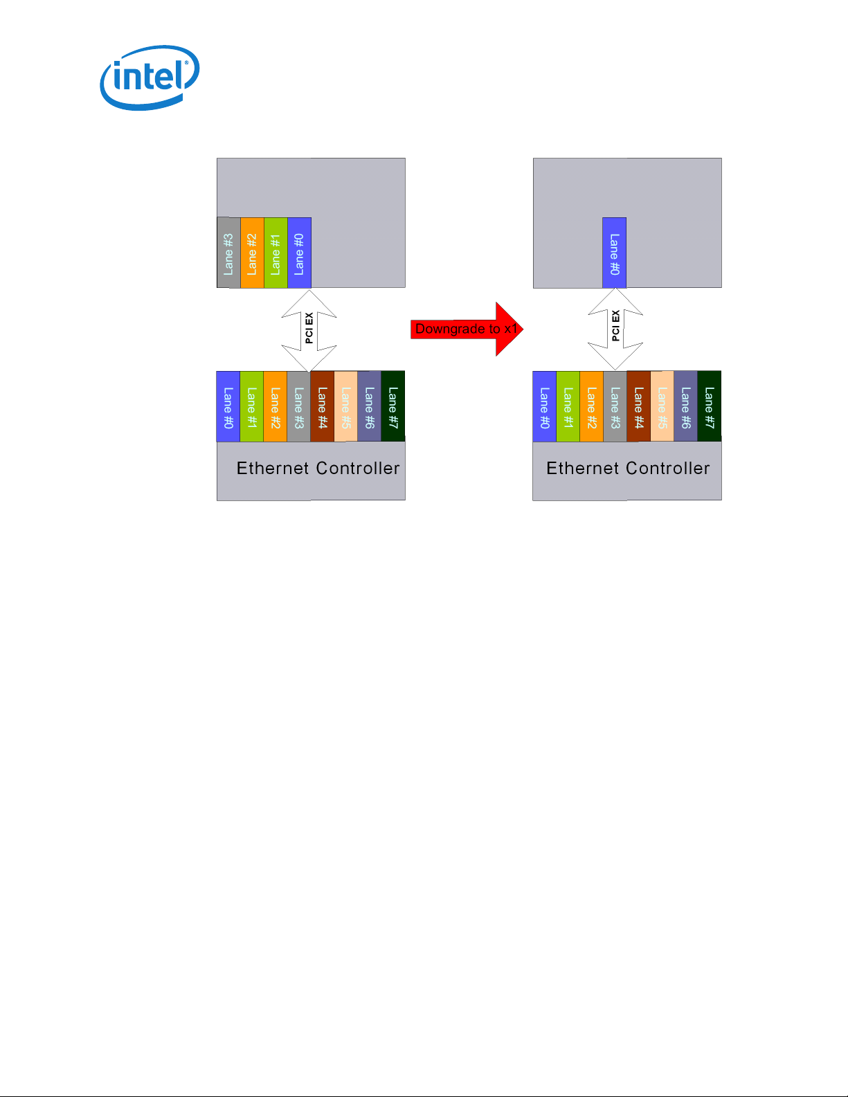
X540 10GBase-T Controller—Interconnects
Figure 3-5 Lane Downshift in an x4 Reversal Configuration
3.1.6.7 Reset
The PCIe PHY supplies the core reset to the X540. The reset can be caused by the
following events:
• Upstream move to hot reset — Inband Mechanism (LTSSM).
• Recovery failure (LTSSM returns to detect)
• Upstream component moves to disable.
3.1.6.8 Scrambler Disable
• The scrambler/de-scrambler functionality in the X540 can be eliminated by three
mechanisms:
• Upstream according to the PCIe specification
• NVM bit — Scram_dis
58
Page 61

Interconnects—X540 10GBase-T Controller
3.1.7 Error Events and Error Reporting
3.1.7.1 General Description
PCIe defines two error reporting paradigms: the baseline capability and the Advanced
Error Reporting (AER) capability. The baseline error reporting capabilities are required of
all PCIe devices and define the minimum error reporting requirements. The AER
capability is defined for more robust error reporting and is implemented with a specific
PCIe capability structure. Both mechanisms are supported by the X540.
The SERR# Enable and the Parity Error bits from the Legacy Command register also take
part in the error reporting and logging mechanism.
In a multi-function device, PCIe errors that are not associated to any specific function
within the device are logged in the corresponding status and logging registers of all
functions in that device. These include the following cases of Unsupported Request (UR):
• A memory or I/O access that does not match any Base Address Register (BAR) for
any function
• Messages
• Configuration accesses to a non-existent function
Figure 3-6 shows, in detail, the flow of error reporting in the X540.
59
Page 62

X540 10GBase-T Controller—Interconnects
Figure 3-6 Error Reporting Mechanism
60
Page 63

Interconnects—X540 10GBase-T Controller
3.1.7.2 Error Events
Table 3-9 lists the error events identified by the X540 and the response in terms of
logging, reporting, and actions taken. Refer to the PCIe specification for the effect on the
PCI Status register.
Table 3-9 Response and Reporting of PCIe Error Events
Error Name Error Events Default Severity Action
Physical Layer Errors
Receiver Error 8b/10b Decode Errors
Packet Framing Error
Data Link Errors
Bad TLP Bad CRC
Illegal EDB
Wrong Sequence Number
Bad DLLP Bad CRC Correctable
Correctable
Send ERR_CORR
Correctable
Send ERR_CORR
Send ERR_CORR
TLP to Initiate NAK, Drop Data
DLLP to Drop
TLP to Initiate NAK, Drop Data
DLLP toDrop
Replay Timer
Timeout
REPLAY NUM
Rollover
Data Link Layer
Protocol Error
TLP Errors
Poisoned TLP
Received
Unsupported
Request (UR)
REPLAY_TIMER expiration Correctable
Send ERR_CORR
REPLAY NUM Rollover Correctable
Send ERR_CORR
Violations of Flow Control
Initialization Protocol
TLP With Error Forwarding Uncorrectable
Wrong Config Access
MRdLk
Config Request Type1
Unsupported Vendor Defined Type
0 Message
Not Valid MSG Code
Not Supported TLP Type
Wrong Function Number
Received TLP Outside Address
Range
Uncorrectable
Send ERR_FATAL
ERR_NONFATAL
Log Header
Uncorrectable
ERR_NONFATAL
Log header
Follow LL Rules
Follow LL Rules
If completion TLP:
Error is non-fatal (default case)
Send error message if advisory
Retry the request once and send advisory
error message on each failure
If fails, send uncorrectable error message
Error is defined as fatal
Send uncorrectable error message
Send Completion With UR
61
Page 64

X540 10GBase-T Controller—Interconnects
Completion Timeout Completion Timeout Timer Expired Uncorrectable
ERR_NONFATAL
Completer Abort Received Target Access With Data
Unexpected
Completion
Receiver Overflow Received TLP Beyond Allocated
Error Name Error Events Default Severity Action
Flow Control
Protocol Error
Malformed TLP (MP) Data Payload Exceed
Size >64 bits
Received Completion Without a
Request For It (Tag, ID, etc.)
Credits
Minimum Initial Flow Control
Advertisements
Flow Control Update for Infinite
Credit Advertisement
Max_Payload_Size
Received TLP Data Size Does Not
Match Length Field
TD field value does not correspond
with the observed size
PM Messages That Don’t Use TC0.
Usage of Unsupported VC
Uncorrectable.
ERR_NONFATAL
Log header
Uncorrectable
ERR_NONFATAL
Log Header
Uncorrectable
ERR_FATAL
Uncorrectable.
ERR_FATAL
Uncorrectable
ERR_FATAL
Log Header
Error is non-fatal (default case)
Send error message if advisory
Retry the request once and send advisory
error message on each failure
If fails, send uncorrectable error message
Error is defined as fatal
Send uncorrectable error message
Send completion with CA
Discard TLP
Receiver Behavior is Undefined
Receiver Behavior is Undefined
Drop the Packet, Free FC Credits
Completion with
Unsuccessful
Completion Status
No Action (already done
by originator of
completion)
Free FC Credits
3.1.7.3 Error Forwarding (TLP Poisoning)
If a TLP is received with an error-forwarding trailer, the packet is dropped and is not
delivered to its destination. The X540 then reacts as listed in Table 3-9.
The X540 does not initiate any additional master requests for that PCI function until it
detects an internal software reset for the associated LAN port. Software is able to access
device registers after such a fault.
System logic is expected to trigger a system-level interrupt to signal the operating
system of the problem. Operating systems can then stop the process associated with the
transaction, re-allocate memory to a different area instead of the faulty area, etc.
62
Page 65

Interconnects—X540 10GBase-T Controller
3.1.7.4 End-to-End CRC (ECRC)
The X540 supports ECRC as defined in the PCIe specification. The following functionality
is provided:
• Inserting ECRC in all transmitted TLPs:
— The X540 indicates support for inserting ECRC in the ECRC Generation Capable
bit of the PCIe configuration registers. This bit is loaded from the ECRC
Generation NVM bit.
— Inserting ECRC is enabled by the ECRC Generation Enable bit of the PCIe
configuration registers.
• ECRC is checked on all incoming TLPs. A packet received with an ECRC error is
dropped. Note that for completions, a completion timeout occurs later (if enabled),
which results in re-issuing the request.
— The X540 indicates support for ECRC checking in the ECRC Check Capable bit of
the PCIe configuration registers. This bit is loaded from the ECRC Check NVM bit.
— Checking of ECRC is enabled by the ECRC Check Enable bit of the PCIe
configuration registers.
• ECRC errors are reported
• System software can configure ECRC independently per each LAN function
3.1.7.5 Partial Read and Write Requests
Partial memory accesses
The X540 has limited support of read and write requests with only part of the byte enable
bits set:
• Partial writes with at least one byte enabled are silently dropped.
• Zero-length writes have no internal impact (nothing written, no effect such as clear-
by-write). The transaction is treated as a successful operation (no error event).
• Partial reads with at least one byte enabled are handled as a full read. Any side effect
of the full read (such as clear by read) is also applicable to partial reads.
• Zero-length reads generate a completion, but the register is not accessed and
undefined data is returned.
Note: The X540 does not generate an error indication in response to any of the
previous events.
Partial I/O accesses
• Partial access on address
— A write access is discarded
— A read access returns 0xFFFF
• Partial access on data, where the address access was correct
— A write access is discarded
— A read access performs the read
63
Page 66

X540 10GBase-T Controller—Interconnects
3.1.7.6 Error Pollution
Error pollution can occur if error conditions for a given transaction are not isolated to the
error's first occurrence. If the PHY detects and reports a receiver error, to avoid having
this error propagate and cause subsequent errors at the upper layers, the same packet is
not signaled at the data link or transaction layers. Similarly, when the data link layer
detects an error, subsequent errors that occur for the same packet are not signaled at
the transaction layer.
3.1.7.7 Completion With Unsuccessful Completion Status
A completion with unsuccessful completion status is dropped and not delivered to its
destination. The request that corresponds to the unsuccessful completion is retried by
sending a new request for undeliverable data.
3.1.7.8 Error Reporting Changes
The PCIe Rev. 1.0 specification defines two changes to advanced error reporting. A (new)
Role Based Error Reporting bit in the Device Capabilities register is set to 1b to indicate
that these changes are supported by the X540.
1. Setting the SERR# Enable bit in the PCI Command register also enables UR reporting
(in the same manner that the SERR# Enable bit enables reporting of correctable and
uncorrectable errors). In other words, the SERR# Enable bit overrides the
Unsupported Request Error Reporting Enable bit in the PCIe Device Control register.
2. Changes in the response to some uncorrectable non-fatal errors detected in nonposted requests to the X540. These are called Advisory Non-Fatal Error cases. For
each of the errors listed, the following behavior is defined:
— The Advisory Non-Fatal Error Status bit is set in the Correctable Error Status
register to indicate the occurrence of the advisory error and the Advisory Non-
Fatal Error Mask corresponding bit in the Correctable Error Mask register is
checked to determine whether to proceed further with logging and signaling.
— If the Advisory Non-Fatal Error Mask bit is clear, logging proceeds by setting the
corresponding bit in the Uncorrectable Error Status register, based upon the
specific uncorrectable error that's being reported as an advisory error. If the
corresponding Uncorrectable Error bit in the Uncorrectable Error Mask register is
clear, the First Error Pointer and Header Log registers are updated to log the
error, assuming they are not still occupied by a previous unserviced error.
— An ERR_COR Message is sent if the Correctable Error Reporting Enable bit is set
in the Device Control register. An ERROR_NONFATAL message is not sent for this
error.
The following uncorrectable non-fatal errors are considered as advisory non-fatal errors:
64
• A completion with an Unsupported Request or Completer Abort (UR/CA) status that
signals an uncorrectable error for a non-posted request. If the severity of the UR/CA
error is non-fatal, the completer must handle this case as an advisory non-fatal error.
Page 67

Interconnects—X540 10GBase-T Controller
• When the requester of a non-posted request times out while waiting for the
associated completion, the requester is permitted to attempt to recover from the
error by issuing a separate subsequent request or to signal the error without
attempting recovery. The requester is permitted to attempt recovery zero, one, or
multiple (finite) times, but must signal the error (if enabled) with an uncorrectable
error message if no further recovery attempt is made. If the severity of the
completion timeout is non-fatal, and the requester elects to attempt recovery by
issuing a new request, the requester must first handle the current error case as an
advisory non-fatal error.
• Receiving a poisoned TLP. See Section 3.1.7.3.
• When a receiver receives an unexpected completion and the severity of the
unexpected completion error is non-fatal, the receiver must handle this case as an
advisory non-fatal error.
3.1.8 Performance Monitoring
The X540 incorporates PCIe performance monitoring counters to provide common
capabilities to evaluate performance. The X540 implements four 32-bit counters to
correlate between concurrent measurements of events as well as the sample delay and
interval timers. The four 32-bit counters can also operate in a two 64-bit mode to count
long intervals or payloads. Software can reset, stop, or start the counters (all at the same
time).
Some counters operate with a threshold — the counter increments only when the
monitored event crossed a configurable threshold (such as the number of available
credits is below a threshold).
Counters operate in one of the following modes:
• Count mode — the counter increments when the respective event occurred
• Leaky Bucket mode — the counter increments only when the rate of events exceeded
a certain value. See Section 3.1.8.1.
The list of events supported by the X540 and the counters Control bits are described in
the PCIe Registers section.
3.1.8.1 Leaky Bucket Mode
Each of the counters can be configured independently to operate in a leaky bucket mode.
When in leaky bucket mode, the following functionality is provided:
• One of four 16-bit Leaky Bucket Counters (LBC) is enabled via the LBC Enable [3:0]
bits in the PCIe Statistic Control register #1.
• The LBC is controlled by the GIO_COUNT_START, GIO_COUNT_STOP,
GIO_COUNT_RESET bits in the PCIe Statistic Control register #1.
• The LBC increments every time the respective event occurs.
• The LBC is decremented every 1 s as defined in the LBC Timer field in the PCIe
Statistic Control registers.
65
Page 68

• When an event occurs and the value of the LBC meets or exceeds the threshold
defined in the LBC Threshold field in the PCIe Statistic Control registers, the
respective statistics counter increments, and the LBC counter is cleared to zero.
3.2 SMBus
SMBus is a management interface for pass-through and/or configuration traffic between
an external Management Controller (MC) and the X540.
3.2.1 Channel Behavior
The SMBus specification defines the maximum frequency of the SMBus as 100 KHz.
However, the SMBus interface can be activated up to 400 KHz without violating any hold
and setup time.
SMBus connection speed bits define the SMBus mode. Also, SMBus frequency support
can be defined only from the NVM.
X540 10GBase-T Controller—Interconnects
3.2.2 SMBus Addressing
The SMBus is presented as two SMBus devices on the SMBus (two SMBus addresses). All
pass-through functionality is duplicated on the SMBus address, where each SMBus
address is connected to a different LAN port.
Note: Designers are not allowed to configure both ports to the same address.
When a LAN function is disabled, the corresponding SMBus address is not
presented to the MC.
The SMBus addresses are set using the SMBus 0 Slave Address and SMBus 1 Slave
Address fields in the NVM.
Note: For the X540 single port configuration, the SMBus Single Port Mode bit
should be set in the NVM, and only the SMBus 0 Slave Address field is valid.
The SMBus addresses (those that are enabled from the NVM) can be re-assigned using
the SMBus ARP protocol.
Besides the SMBus address values, all the previously listed parameters of the SMBus
(SMBus channel selection, single port mode, and address enable) can be set only through
the NVM.
All SMBus addresses should be in Network Byte Order (NBO) with the most significant
byte first.
66
Page 69

Interconnects—X540 10GBase-T Controller
3.2.3 SMBus Notification Methods
The X540 supports three methods of signaling the external MC that it has information
that needs to be read by the external MC:
• SMBus alert — Refer to Section 3.2.3.1.
• Asynchronous notify — Refer to Section 3.2.3.2.
• Direct receive — Refer to section Section 3.2.3.3.
The notification method that is used by the X540 can be configured from the SMBus
using the Receive Enable command. The default method is set from the Notification
Method field in NVM word LRXEN1.
The following events cause the X540 to send a notification event to the external MC:
• Receiving a LAN packet, designated for the MC.
• Receiving a Request Status command from the MC that initiates a status response.
• The X540 is configured to notify the external MC upon status changes (by setting the
EN_STA bit in the Receive Enable Command) and one of the following events happen:
• TCO Command Aborted
• Link Status changed
• Power state change
• MACsec indication.
There can be cases where the external MC is hung and cannot not respond to the SMBus
notification. The X540 has a timeout value defined in the NVM (refer to Section 6.5.4.3)
to avoid hanging while waiting for the notification response. If the MC does not respond
until the timeout expires, the notification is de-asserted.
3.2.3.1 SMBus Alert and Alert Response Method
SMBALRT_N (SMBus Alert) is an additional SMBus signal that acts as an asynchronous
interrupt signal to an external SMBus master. The X540 asserts this signal each time it
has a message that it needs the external MC to read and if the chosen notification
method is the SMBus alert method.
Note: SMBALRT_N is an open-drain signal, which means that devices other than
the X540 can be connected to the same alert pin. The external MC requires
a mechanism to distinguish between the alert sources as follows:
The external MC responds to the alert by issuing an Alert Response Address (ARA) cycle
to detect the alert source device. The X540 responds to the ARA cycle (if it was the
SMBus alert source) and de-asserts the alert when the ARA cycle completes. Following
the ARA cycle, the MC issues a Read command to retrieve the the X540 message.
Note: Some MCs do not implement the ARA cycle transaction. These MCs respond
to an alert by issuing a Read command to the X540 (0xC0/0xD0 or 0xDE).
The X540 always responds to a Read command even if it is not the source of
the notification. The default response is a status transaction. If the X540 is
the source of the SMBus alert, it replies to the read transaction.
67
Page 70

X540 10GBase-T Controller—Interconnects
The ARA cycle is an SMBus receive byte transaction to SMBus Address 0x18.
Note: The ARA transaction does not support PEC.
The alert response address transaction format is as follows:
17 11811
S ARA Rd A Slave Device Address A P
0001 100 0 0 1
Figure 3-7 SMBus ARA Cycle Format
3.2.3.2 Asynchronous Notify Method
When configured using the asynchronous notify method, the X540 acts as an SMBus
master and notifies the external MC by issuing a modified form of the write word
transaction. The asynchronous notify transaction SMBus address and data payload are
configured using the Receive Enable command or by using the NVM defaults (see
Section 6.5.3.20).
Note: The asynchronous notify is not protected by a PEC byte.
1711711
S Target Address Wr A Sending Device Address A
MC Slave Address 0 0 Manageability Slave SMBus
Address
81 8 11
Data Byte Low A Data Byte High A P
Interface 0 Alert Value 0
00
Figure 3-8 Asynchronous Notify Command Format
3.2.3.3 Direct Receive Method
If configured, the X540 has the capability to send the message it needs to transfer to the
external MC, as a master over the SMBus instead of alerting the MC and waiting for it to
read the message.
The message format is shown in Figure 3-9. Note that the command that should be used
is the same command that should be used by the MC in the Block Read command and the
opcode that the X540 puts in the data is the same as it would have put in the Block Read
command of the same functionality. The rules for the F and L flags are also the same as
in the Block Read command.
68
Page 71

Interconnects—X540 10GBase-T Controller
171111 61
S Target Address Wr A F L Command A
First
MC Slave Address 0 0
81 8 1 1 8 11
Byte Count A Data Byte 1 A A Data Byte N A P
N0 0 0 0
Flag
Last
Flag
Receive TCO Command
Figure 3-9 Direct Receive Transaction Format
3.2.4 Receive TCO Flow
The X540 is used as a channel for receiving packets from the network link and passing
them to an external MC. The MC can configure the X540 to pass specific packets to the
MC (see Section 11.2). Once a full packet is received from the link and identified as a
manageability packet that should be transferred to the MC, the X540 starts the receive
TCO transaction flow to the MC.
The maximum SMBus fragment length is defined in the NVM (see Section 6.5.4.2). The
X540 uses the SMBus notification method to notify the MC that it has data to deliver. The
packet is divided into fragments, where the X540 uses the maximum fragment size
allowed in each fragment. The last fragment of the packet transfer is always the status of
the packet. As a result, the packet is transferred in at least two fragments. The data of
the packet is transferred in the receive TCO LAN packet transaction.
01 0000b
0
When SMBus Alert is selected as the MC notification method, the X540 notifies the MC on
each fragment of a multi-fragment packet.
When asynchronous notify is selected as the MC notification method, the X540 notifies
the MC only on the first fragment of a received packet. It is the MC's responsibility to
read the full packet including all the fragments.
Any timeout on the SMBus notification results in discarding of the entire packet. Any
NACK by the MC on one of the X540's receive bytes also causes the packet to be silently
discarded.
Since SMBus throughput is lower than the network link throughput, the X540 uses an 8
KB internal buffer per LAN port, which stores incoming packets prior to being sent over
the SMBus interface. The X540 services back-to-back management packets as long as
the buffer does not overflow.
The maximum size of the received packet is limited by the X540 hardware to 1536 bytes.
Packets larger then 1536 bytes are silently discarded. Any packet smaller than 1536
bytes is processed by the X540.
Note: When the RCV_EN bit is cleared, all receive TCO functionality is disabled
including packets directed to the MC as well as auto ARP processing.
69
Page 72

3.2.5 Transmit TCO Flow
The X540 is used as a channel for transmitting packets from the external MC to the
network link. The network packet is transferred from the external MC over the SMBus,
and then, when fully received by the X540, is transmitted over the network link.
In dual-address mode, each SMBus address is connected to a different LAN port. When a
packet received in SMBus transactions using SMBus 0 Slave Address, it is transmitted to
the network using LAN port 0 and is transmitted through LAN port 1 if received on SMB
address 1. In single-address mode, the transmitted port is chosen according to the failover algorithm (see Section 11.2.2.2).
The X540 supports packets up to an Ethernet packet length of 1536 bytes. SMBus
transactions can be up to 240 bytes in length, which means that packets can be
transferred over the SMBus in more than one fragment. In each command byte there are
the F and L bits. When the F bit is set, it means that this is the first fragment of the
packet and L means that it is the last fragment of the packet (when both are set, it
means that the entire packet is in one fragment). The packet is sent over the network
link only after all its fragments have been received correctly over the SMBus.
The X540 calculates the L2 CRC on the transmitted packet, and adds its four bytes at the
end of the packet. Any other packet field (such as XSUM) must be calculated and inserted
by the external MC (the X540 does not change any field in the transmitted packet other
than adding padding and CRC bytes). If the packet sent by the MC is bigger than 1536
bytes, then the packet is silently discard by the X540.
X540 10GBase-T Controller—Interconnects
The minimum packet length defined by the 802.3 specification is 64 bytes. The X540
pads packets that are less than 64 bytes to meet the specification requirements (no need
for the external MC to do it). There is one exception, that is if the packet sent over the
SMBus is less than 32 bytes, the MC must pad it for at least 32 bytes. The passing bytes
value should be zero. Packets that are smaller then 32 bytes (including padding) are
silently discarded by the X540.
If the network link is down when the X540 has received the last fragment of the packet,
it silently discards the packet.
Note: Any link down event while the packet is being transferred over the SMBus
does not stop the operation, since the X540 waits for the last fragment to
end to see whether the network link is up again.
The transmit SMBus transaction is described in Section 11.7.2.1.
3.2.5.1 Transmit Errors in Sequence Handling
Once a packet is transferred over the SMBus from the MC to the X540 the F and L flags
should follow specific rules. The F flag defines that this is the first fragment of the packet,
and the L flag defines that the transaction contains the last fragment of the packet.
Table 3-10 lists the different option of the flags in transmit packet transactions.
70
Page 73

Interconnects—X540 10GBase-T Controller
Table 3-10 SMBus Transmit Sequencing
Previous Current Action/Notes
Last First Accept both.
Last Not First Error for current transaction. Current transaction is discarded and an abort status is asserted.
Not Last First Error for previous transaction. The previous transaction (until the previous first) is discarded. The
Not Last Not First The X540 can process the current transaction.
current packet is processed.
No abort status is asserted.
Note: Since every other Block Write command in the TCO protocol has both the
First (F) and Last (L) flags on, they cause flushing any pending transmit
fragments that were previously received. As such, when running the TCO
transmit flow, no other Block Write transactions are allowed in between the
fragments.
3.2.5.2 TCO Command Aborted Flow
Bit 6 in first byte of the status returned from the X540 to the external MC indicates that
there was a problem with previous SMBus transactions or with the completion of the
operation requested in previous transaction.
The abort can be asserted due to any of the following reasons:
• Any error in the SMBus protocol (NACK, SMBus time-outs).
• Any error in compatibility due to required protocols to specific functionality (Rx
Enable command with byte count not 1/14 as defined in the command specification).
• If the X540 does not have space to store the transmit packet from the MC (in an
internal buffer) before sending it to the link. In this case, all transactions are
completed but the packet is discarded and the BMC is notified through the Abort bit.
• Error in First/Last bit sequence during multi-fragment transactions.
• The Abort bit is asserted after an internal reset to the X540 manageability unit.
Note: The abort in the status does not always imply that the last transaction of
the sequence was bad. There is a time delay between the time the status is
read from the X540 and the time the transaction has occurred.
3.2.6 Concurrent SMBus Transactions
Concurrent SMBus write transactions are not permitted. Once a transaction is started, it
must be completed before additional transaction can be initiated.
71
Page 74

X540 10GBase-T Controller—Interconnects
3.2.7 SMBus ARP Functionality
The X540 supports the SMBus ARP protocol as defined in the SMBus 2.0 specification.
The X540 is a persistent slave address device when its SMBus address is valid after
power-up and loaded from the NVM. The X540 also supports all SMBus ARP commands
defined in the SMBus specification, both general and directed.
Note: SMBus ARP can be disabled through NVM configuration (See
Section 6.5.4.3).
3.2.7.1 SMBus ARP
the X540 responds as two SMBus devices, in which it has two sets of AR/AV flags — one
for each port. The X540 should respond twice to the SMBus-ARP master, one time for
each port. Both SMBus addresses are taken from the SMBus-ARP addresses word of the
NVM. The UDID is different between the two ports in the version ID field, which
represents the Ethernet MAC address, which is different between the two ports. It is
recommended for the X540 to first answer as port 0, and only when the address is
assigned, to answer as port 1 to the Get UDID command.
3.2.7.2 SMBus-ARP Flow
SMBus-ARP flow is based on the status of two AVs and ARs:
• Address Valid — This flag is set when the X540 has a valid SMBus address.
• Address Resolved — This flag is set when the X540 SMBus address is resolved:
SMBus address was assigned by the SMBus-ARP process.
Note: These flags are internal the X540 flags and not shown to external SMBus
devices.
Since the X540 is a Persistent SMBus Address (PSA) device, the AV flag is always set,
while the AR flag is cleared after power-up until the SMBus-ARP process completes. Since
AV is always set, it means that the X540 always has a valid SMBus address. The entire
SMBus ARP Flow is described in Figure 3-10.
When the SMBus master needs to start the SMBus-ARP process, it resets (in terms of
ARP functionality) all the devices on the SMBus, by issuing either Prepare to ARP or Reset
Device commands. When the X540 accepts one of these commands, it clears its AR flag
(if set from previous SMBus-ARP process), but not its AV flag (The current SMBus
address remains valid until the end of the SMBus ARP process).
A cleared AR flag means that the X540 answers the following SMBus ARP transactions
that are issued by the master. The SMBus master then issues a Get UDID command
(General or Directed), to identify the devices on the SMBus. The X540 responds to the
Directed command all the time, and to the General command only if its AR flag is not set.
After the Get UDID, the master assigns the X540 SMBus address, by issuing Assign
Address command. The X540 checks whether the UDID matches its own UDID, and if
there is a match it switches its SMBus address to the address assigned by the command
(byte 17). After accepting the Assign Address command, the AR flag is set, and from this
point (as long as the AR flag is set), the X540 does not respond to the Get UDID General
command, while all other commands should be processed even if the AR flag is set.
72
Page 75

Interconnects—X540 10GBase-T Controller
After SMBus ARP is successfully carried out, the new address is stored in the NVM, and
will thus be the address used at the next power up.
Figure 3-10 SMBus-ARP Flow
3.2.8 Fairness Arbitration
When sending MCTP messages over SMBus and when fairness arbitration is enabled (see
Section 6.5.4.3), the X540 should respect the fairness arbitration as defined in section
5.13 of DSP0237 when sending MCTP messages.
73
Page 76

X540 10GBase-T Controller—Interconnects
3.3 Network Controller — Sideband Interface (NC-SI)
The NC-SI interface in the X540 is a connection to an external MC.
The X540 NC-SI interface meets the NC-SI version 1.0.0 specification as a PHY-side
device.
3.3.1 Electrical Characteristics
The X540 complies with the electrical characteristics defined in the NC-SI specification.
3.3.2 NC-SI Transactions
Compatible with the NC-SI specification.
3.4 Non-Volatile Memory (NVM)
3.4.1 General Overview
The X540 uses a Flash device for storing product configuration information. The Flash is
divided into three general regions:
• Hardware Accessed — Loaded by the X540 hardware after power-up, PCI reset deassertion, D3 to D0 transition, or software reset. Different hardware sections in the
Flash are loaded at different events. For more details on power-up and reset
sequences, see Section 4.0.
• Firmware Area — Includes structures used by the firmware for management
configuration in its different modes.
• Software Accessed — This region is used by software entities such as LAN drivers,
option ROM software and tools, PCIe bus drivers, VPD software, etc.
3.4.2 Flash Device Requirements
The X540 merges the 82599 legacy EEPROM and Flash content in a single Flash device.
Flash devices require a sector erase instruction in case a cell is modified from 0b to 1b.
As a result, in order to update a single byte (or block of data) it is required to erase it
first. The X540 supports Flash devices with a sector erase size of 4 KB. Note that many
Flash vendors are using the term sector differently. The X540 Datasheet uses the term
Flash sector for a logic section of 4 KB.
74
Page 77

Interconnects—X540 10GBase-T Controller
The X540 supports Flash devices that are either write-protected by default after powerup or not. The X540 is responsible to remove the protection by sending the writeprotection removal OpCode to the Flash after power up.
The following OpCodes are supported by the X540 as they are common to all supported
Flash devices:
1. Write Enable (0x06)
2. Read Status Register (0x05)
3. Write Status Register (0x01). The written data is 0x00 to cancel the Flash default
protection.
4. Read Data (0x03). Burst read is supported.
5. Byte/Page Program (0x02). To program 1 to 256 data bytes.
6. 4 KB Sector-Erase (0x20)
7. Chip-Erase (0xC7)
3.4.3 Shadow RAM
The X540 maintains the first two 4 KB sectors, Sector 0 and Sector 1, for the
configuration content. At least one of these two sectors must be valid at any given time
or else the X540 is set by hardware default. Following a Power On Reset (POR) the X540
copies the valid lower 4 KB sector of the Flash device into an internal shadow RAM. Any
further accesses of the software or firmware to this section of the NVM are directed to the
internal shadow RAM. Modifications made to the shadow RAM content are then copied by
the X540 into the other 4KB sector of the NVM, flipping circularly the valid sector
between sector 0 and 1 of NVM.
This mechanism provides the following advantage:
1. A seamless backward compatible read/write interface for software/firmware to the
first 4 KB of the NVM as if an external EEPROM device were connected. This interface
is referred as EEPROM-Mode access to the Flash.
2. A way for software to protect image-update procedure from power down events by
establishing a double-image policy. See Section 6.2.1.1 for a description of the
double-image policy. It relies on having pointers to all the other NVM modules
mapped in the NVM sector which is mirrored in the internal shadow RAM.
Figure 3-11 shows the shadow RAM mapping and interface.
75
Page 78

X540 10GBase-T Controller—Interconnects
Figure 3-11 NVM Shadow RAM
Following a write access by software or firmware to the shadow RAM, the data should
finally be updated in the Flash as well. The X540 updates the Flash from the shadow RAM
when software/firmware requests explicitly to update the Flash by setting the FLUPD bit
in the EEC register. For saving Flash updates, it is expected that software/firmware set
the FLUPD bit only once it has completed their last write access to the Flash. The X540
then copies the content of the shadow RAM to the non-valid configuration sector and
makes it the valid one. The Flash update sequence handled by the device is listed in the
steps that follow:
1. Initiate sector erase instruction(s) to the non-valid sector, either sector 0 or sector 1
(the non-valid sector is defined by the inverse value of the SEC1VAL bit in the EEC
register).
2. Copy the shadow RAM to the non-valid sector, with the signature field present in NVM
Control Word 1 copied last.
3. Toggle the state of the SEC1VAL bit in the EEC register to indicate that the non-valid
sector became the valid one and visa versa.
4. Clear the signature field in the valid sector to make it invalid. Since a valid signature
is 01b, it is enough to program the bits to 00b, without issuing a sector erase
command to the Flash.
Note: Software should be aware that programming the Flash might require a long
latency due to the Flash update sequence handled by hardware. The sector
erase command by itself can last tens of s. Software must poll the
FLUDONE bit in the EEC register to check whether or not the Flash
programming completed.
76
Note: The X540 always effectively updates the Flash after any VPD write access
(no use of the EEC.FLUPD bit is required in this case).
Page 79

Interconnects—X540 10GBase-T Controller
Note: Contents of the shadow RAM is reset only at LAN_PWR_GOOD events. It is
protected against an ECC error at the shell level in such a way that the
probability of an error is close to zero.
Note: Each time the Flash content is not valid (blank configuration sectors or
wrong signature on both sector 0 and 1) EEPROM access mode is turned off.
Software should rather use either the bit banging interface to the Flash
through FLA register or the memory mapped Flash BAR access.
3.4.4 NVM Clients and Interfaces
Note: Access to the NVM should be done exactly according to the flows described
in this section. Any read or write access to the NVM that does not follow
exactly to the rules and steps listed in this section might lead to unexpected
results.
There are several clients that can access the NVM to different address ranges via
different access modes, methods, and interfaces. The various clients to the NVM are
Software Tools (BIOS, etc.), Drivers, MC (via Firmware), and VPD Software.
Table 3-11 lists the different accesses to the NVM.
Table 3-11 Clients and Access Types to the NVM
NVM
Client
VPD Software Parallel (32-bits) EEPROM 0x000000 -
Software Parallel (16-bits) EEPROM 0x000000 -
Software Bit Banging (1-bit) Flash 0x000000 -
Access
Method
Parallel (32-bits
read, 8-bits write)
NVM Access
Mode
Flash 0x000000 -
Flash 0x002000 -
Logical Byte
Address Range
0x000FFF
0x000FFF
0x001FFF
0xFFFFFF
0x001FFF
0x002000 0xFFFFFFF
Note: Firmware saves words like SMBus Slave Addresses or Signature, which are
saved into the NVM at the firmware’s initiative. Note that the VPD module
must be mapped to the first valid 4 KB sector.
NVM Access Interface (CSRs or Other)
VPD Address and Data registers, via shadow RAM
logic. Any write access is immediately pushed by
the X540 into the Flash. VPD module must be
located in the first valid Flash sector.
EERD, EEWR, via shadow RAM logic.
Memory mapped via BARs. Accessing this range
via Flash BAR should be avoided during normal
operation as it might cause non-coherency
between the Flash and the shadow RAM.
Memory mapped via BARs.
FLA. Accessing this range via bit-banging should
be avoided during normal operation as it might
cause non-coherency between the Flash and the
shadow RAM.
FLA
77
Page 80

X540 10GBase-T Controller—Interconnects
3.4.4.1 Memory Mapped Host Interface
Using the legacy Flash transactions the Flash is read from, or written to, by the X540
each time the host CPU performs a read or a write operation to a memory location that is
within the Flash address mapping or upon boot via accesses in the space indicated by the
Expansion ROM Base Address register. Accesses to the Flash are based on a direct
decode of CPU accesses to a memory window defined in either:
• Memory CSR + Flash Base Address Register (PCIe Control Register at offset 0x10).
• The Expansion ROM Base Address Register (PCIe Control Register at offset 0x30).
• The X540 is responsible to map accesses via the Expansion ROM BAR to the physical
NVM. The offset in the NVM of the Expansion ROM module is defined by the PCIe
Expansion/Option ROM Pointer (Flash word address 0x05). This pointer is loaded by
the X540 from the Flash before enabling any access to the Expansion ROM memory
space.
— When modifying the PXE Driver Section Pointer in the NVM, it is required to issue
a PCIe reset on which the updated offset is sampled by the hardware.
— In case there is no valid NVM signature in the two first 4 KB sectors, then
expansion ROM BAR is disabled.
Note: The X540 controls accesses to the Flash when it decodes a valid access.
Attempt to out of range write access the PCIe Expansion/Option ROM
module (according to NVM size field in NVM Control Word 1) is ignored,
while read access would return value of 0xDEADBEAF. The X540 supports
only byte writes to the Flash.
Note: Flash read accesses are assembled by the X540 each time the access is
greater than a byte-wide access.
Note: The X540 byte reads or writes to the Flash take about 2-30 s time. The
device continues to issue retry accesses during this time.
Note: During normal operation, the host should avoid memory mapped accesses
to the first two 4 KB sectors of the Flash because it might be non-coherent
with the shadow RAM contents.
Caution: Flash BAR access while FLA.FL_REQ is asserted (and granted) is forbidden.
It can lead to a PCIe hang as a bit-banging access requires several PCIe
accesses.
3.4.4.2 CSR Mapped Host Interface
Software has bit banging or parallel accesses to the NVM or to the shadow RAM (refer to
Table 3-11) via registers in the CSR space. The X540 supports the following cycles on the
parallel interface: posted write, posted read, sector erase and device erase.
3.4.4.2.1 EEPROM-Mode Host Interface
EEPROM-Mode provides a parallel interface to the first valid 4KB sector of the NVM, aka
base sector, which is agnostic to the Flash device type. It also minimizes excessive sector
erase cycles to the Flash device by coalescing an update of the whole base sector to a
single programming cycle.
78
Page 81

Interconnects—X540 10GBase-T Controller
3.4.4.2.2 Bit Banging Host Interface
Software can access the Flash directly by using the Flash's 4-wire interface through the
Flash Access (FLA) register. It can use this for reads, writes, or other Flash operations
(accessing the Flash status register, erase, etc.).
3.4.4.3 MC Interface
The MC can access several fields in the NVM and/or shadow RAM via dedicated NC-SI
commands.
3.4.5 Flash Access Contention
Flash accesses initiated through the LAN "A" device and those initiated through the LAN
"B" device may occur during the same approximate size window. The X540 does not
synchronize between the two entities accessing the Flash so contentions caused from one
entity reading and the other modifying the same locations is possible.
To avoid such a contention between software LANs or between software and firmware
accesses, these entities are required to make use of the semaphore registers. Refer to
Section 11.7.5. Any read or write access to the NVM made by software/firmware must be
preceded by acquiring ownership over the NVM. This is also useful to avoid the timeout of
the PCIe transaction made to a memory mapped Flash address while the Flash is
currently busy with a long sector erase operation.
Two software entities could however not use the semaphore mechanism: BIOS and VPD
software.
• Since VPD software accesses only the VPD module, which is located in the first valid
sector of the NVM, VPD accesses are always performed against the shadow RAM first.
In this case, hardware must take/release ownership over the NVM as if it was the
originator of the Flash access. It is then hardware’s responsibility to update the NVM
according to the Flash update sequence described in Shadow RAM.
• No contention can occur between BIOS and any other software entity (VPD included)
as it accesses the NVM while the operating system is down.
• Contention between BIOS and firmware can however happen if a system reboot
occurs while the MC is accessing the NVM.
— If a system reboot is caused by a user pushing on the standby button, it is
required to route the wake-up signal from the standby button to the MC and not
to the chipset. The MC issues a system reboot signal to the chipset only after the
NVM write access completes. Firmware is responsible to poll whether the NVM
write has completed before sending the response to the MC NC-SI command.
— If a system reboot is issued by a local user on the host, there is no technical way
to avoid NVM access contention between BIOS and the MC to occur.
Caution: It is the user’s responsibility when accessing the NVM remotely via the MC
to make sure another user in not currently initiating a local host reboot
there.
79
Page 82

X540 10GBase-T Controller—Interconnects
Note: The PHY auto-load process from the Flash device is made up of short read
bursts (32-bits) that can be inserted by hardware in between other NVM
clients’ accesses, at the lowest priority. It is the user’s responsibility to
avoid initiating PHY auto-load while updating the PHY NVM modules.
Note: The MAC auto-load from the Flash device itself occurs only after power-up
and before host or firmware can attempt to access the Flash. The host must
wait until PCIe reset is de-asserted (after ~1 sec, which is enough time for
the MAC auto-load to complete), and firmware starts its auto-load after the
EEC.AUTO_RD bit is asserted by hardware.
Note: Other MAC auto-load events are performed from the internal shadow RAM
which do not compete with memory mapped accesses to the Flash device.
During such MAC auto-load, accesses from other clients via EEPROM-Mode
registers are delayed until the auto-load process completes.
Note: Software and firmware should avoid holding Flash ownership (via the
dedicated semaphore bit) for more than 500 ms.
3.4.6 NVM Read, Write, and Erase Sequences
Refer to Section 6.2.1.1 to establish the required double-image policy prior to updating
any Flash module.
Any software or firmware flow described in this section (excepted for VPD and BIOS) shall
be preceded by taking NVM ownership via semaphores as described in Section 11.7.5.
3.4.6.1 Flash Erase Flow by the Host
1. Erase access to the Flash must first be enabled by clearing the FWE field in the EEC
register.
2. Poll the FL_BUSY flag in the FLA register until cleared.
3. Set the Flash Device Erase bit (FL_DER) in the FLA register or the Flash Sector Erase
bit (FL_SER) together with the Flash sector index to be erased (FL_SADDR).
4. Clear the erase enable by setting the FWE field to 01b in the EEC register to protect
the Flash device.
Note: Trying to erase a sector in the Flash device when writes are disable
(FWE=01b) cannot be performed by the X540.
Hardware gets the Erase command from FLA register and sends the corresponding Erase
command to the Flash. The erase process then finishes by itself. Software should wait for
the end of the erase process before any further access to the Flash. This can be checked
by polling the FLA.FL_BUSY bit.
80
Page 83

Interconnects—X540 10GBase-T Controller
3.4.6.2 Software Flow to the Bit Banging Interface
To directly access the Flash, software should follow these steps:
1. Write a 1b to the Flash Request bit (FLA.FL_REQ).
2. Read the Flash Grant bit (FLA.FL_GNT) until it becomes 1b. It remains 0b as long as
there are other accesses to the Flash.
3. Write or read the Flash using the direct access to the 4-wire interface as defined in
the FLA register. The exact protocol used depends on the Flash placed on the board
and can be found in the appropriate datasheet.
4. Write a 0b to the Flash Request bit (FLA.FL_REQ).
5. Following a write or erase instruction, software should clear the Request bit only after
it has checked that the cycles were completed by the NVM. This can be checked by
reading the BUSY bit in the Flash device STATUS register. Refer to Flash datasheet for
the opcode to be used for reading the STATUS register.
Note: Bit Banging Interface is not expected to be used during nominal operation.
Software/firmware should rather use the EEPROM-Mode when accessing the
base sector and the Flash-Mode for other sectors.
Note: If software must use the Bit Banging Interface in nominal operation it
should adhere to the following rules:
• Gain access first to the Flash using the flow described in Section 11.7.5
• Minimize FLA.FL_REQ setting for a single byte/word/dword access or
other method that guarantee fast enough release of the FLA.FL_REQ.
3.4.6.3 Software Word Program Flow to the EEPROMMode Interface
Read Interface:
Software initiates a read cycle to the NVM via the EEPROM-mode by writing the address
to be read and the Start bit to the EERD register.
As a response, hardware executes the following steps:
1. The X540 reads the data from the shadow RAM.
2. Puts the data in Data field of the EERD register.
3. Sets the Done bit in the EERD register.
Note: Any word read this way is not loaded into the X540's internal registers. This
happens only at an hardware auto-load event.
Write Interface:
Software initiates a write cycle to the NVM via the EEPROM-mode as follows:
1. Poll the Done bit in the EEWR register until its set.
2. Write the data word, its address, and the Start bit to the EEWR register.
As a response, hardware executes the following steps:
1. The X540 writes the data to the shadow RAM.
81
Page 84

X540 10GBase-T Controller—Interconnects
2. The X540 sets the Done bit in the EEWR register.
Note: In addition, the VPD area of the NVM can be accessed via the PCIe VPD
capability structure.
Note: EEPROM-Mode writes are performed into the internal shadow RAM.
Section 6.2.1.1 describes the procedure for copying the internal shadow
RAM content into the base sector of the Flash device.
3.4.6.4 Flash Program Flow via the Memory Mapped Interface
Software initiates a write cycle via the Flash BAR as follows:
1. Enable Flash BAR writes by setting EEC.FWE to 10b.
2. Poll the FL_BUSY flag in the FLA register until cleared.
3. Write the data byte to the Flash through the Flash BAR.
4. Repeat the steps 2 and 3 if multiple bytes should be programmed.
5. Disable Flash BAR writes by setting EEC.FWE to 01b.
As a response, hardware executes the following steps for each write access:
1. Set the FL_BUSY bit in the FLA register.
2. Initiate autonomous write enable instruction.
3. Initiate the program instruction right after the enable instruction.
4. Poll the Flash status until programming completes.
5. Clear the FL_BUSY bit in the FLA register.
Note: Software must erase the sector prior to programming it.
3.4.7 Signature Field
The only way The X540 can tell if a Flash is present is by trying to read the Flash. The
X540 first reads the Control word at word address 0x000000 and at word address
0x000800. It then checks the signature value at bits 7 and 6 in both addresses.
If bit 7 is 0b and bit 6 is 1b in (at least) one of the two addresses, it considers the Flash
to be present and valid. It then reads the additional Flash words and programs its
internal registers based on the values read. Otherwise, it ignores the values it reads from
that location and does not read any other words.
If the signature bits are valid at both addresses the X540 assumes that the base sector
starts at address zero.
82
Page 85

Interconnects—X540 10GBase-T Controller
3.4.8 Flash Recovery
The first two sectors of the Flash contains fields that if programmed incorrectly might
affect the functionality of the X540. The impact might range from an incorrect setting of
some function (like LED programming), via disabling of entire features (such as no
manageability) and link disconnection, to the inability to access the device via the regular
PCIe interface.
The X540 implements a mechanism that enables recovery from a faulty Flash no matter
what the impact is, using an SMBus message that instructs the firmware to invalidate the
first two sectors of the Flash.
This mechanism uses an SMBus message that the firmware is able to receive in all
modes, no matter what is in the content of the first two sectors of the Flash. After
receiving this message, firmware erases the first two sectors of the Flash that sets word
0x0 to 0xFF invalidating the signature BIOS or the operating system initiates a power
event to force a Flash auto-load process that fails and enables access to the device.
The firmware is programmed to receive such a command only from PCIe reset until one
of the functions changes its status from D0u to D0a. Once one of the functions moves to
D0a it can be safely assumed that the device is accessible to the host and there is no
further need for this function. This reduces the possibility of malicious software to use
this command as a back door and limits the time the firmware must be active in nonmanageability mode.The command is sent on a fixed SMBus address of 0xC8. The format
of the command is SMBus Block Write is as follows:
Function Command Data Byte
Release Flash 0xC7 0x12
Note: This solution requires a controllable SMBus connection to the X540.
Note: In case more than one the X540 is in a state to accept this solution, all of
the X540 devices connected to the same SMBus accept the command. The
devices in D0u state erase the first two sectors of the Flash.
After receiving a Release Flash command, firmware should keep its current state. It is the
responsibility of the user updating the Flash to send a firmware reset if required after the
entire Flash update process is done.
Data byte 0x12 is the LSB of the X540's default Device ID. The 82575, for example, uses
the same command but the data byte there is 0xAA.
An additional command is introduced to enable the write from the SMBus interface
directly into any MAC CSR register. The same rules as for the Release Flash command
that determine when the firmware accepts this command apply to this command as well.
The command is sent on a fixed SMBus address of 0xC8. The format of the command is
SMBus Block Write is as follows:
Function Command Byte Count Data 1 Data 2 Data 3 Data 4 … Data 7
CSR Write 0xC8 7
Config Address 2Config Address 1Config Address 0Config Data
MSB
… Config Data LSB
83
Page 86

X540 10GBase-T Controller—Interconnects
The MSB in Configuration Address 2 indicates which port is the target of the access (0 or
1).
The X540 always enables the manageability block after power up. The manageability
clock is stopped only if the manageability function is disabled in the Flash and one of the
functions had transitioned to D0a; otherwise, the manageability block gets the clock and
is able to wait for the new command.
This command allows writing to any MAC or PHY CSR register as part of the Flash
recovery process. This command can be used to write to the Flash and update different
sections in it.
3.4.9 Flash Deadlock Avoidance
The Flash is a shared resource between the following clients:
1. Hardware auto-read.
2. LAN port 0 and LAN port 1 software accesses.
3. Manageability/firmware accesses.
4. Software tools.
All clients can access the Flash using parallel access, on which hardware implements the
actual access to the Flash. Hardware schedules these accesses, avoiding starvation of
any client.
However, the software and firmware clients can access the Flash using bit banging. In
this case, there is a request/grant mechanism that locks the Flash to the exclusive use of
one client. If one client is stuck without releasing the lock, the other clients can no longer
access the Flash. To avoid this deadlock, the X540 implements a timeout mechanism,
which releases the grant from a client that holds the Flash bit-bang interface
(FLA.FL_SCK bit) for more than 2 seconds. If any client fails to release the Flash
interface, hardware clears its grant enabling the other clients to use the interface.
Note: The bit banging interface does not guarantee fairness between the clients,
therefore it should be avoided in nominal operation as much as possible.
When write accesses to the Flash are required the software or
manageability should access the Flash one word at a time releasing the
interface after each word. Software and firmware should avoid holding the
Flash bit-bang interface for more than 500 ms.
The deadlock timeout mechanism is enabled by the Deadlock Timeout Enable bit in the
Control Word 2 in the Flash.
3.4.10 VPD Support
84
The Flash image can contain an area for VPD. This area is managed by the OEM vendor
and does not influence the behavior of hardware. Word 0x2F of the Flash image contains
a pointer to the VPD area in the Flash. A value of 0xFFFF means VPD is not supported and
the VPD capability does not appear in the configuration space.
Page 87

Interconnects—X540 10GBase-T Controller
The maximal area size is 256 bytes but can be smaller. The VPD block is built from a list
of resources. A resource can be either large or small. The structure of these resources
are listed in the following tables.
Table 3-12 Small Resource Structure
Offset 0 1 — n
Content Tag = 0xxx,xyyyb (Type = Small(0), Item Name = xxxx, length = yy bytes) Data
Table 3-13 Large Resource Structure
Offset 0 1 — 2 3 — n
Content Tag = 1xxx,xxxxb (Type = Large(1), Item Name = xxxxxxxx) Length Data
The X540 parses the VPD structure during the auto-load process following PCIe reset in
order to detect the read only and read/write area boundaries. The X540 assumes the
following VPD fields with the limitations listed:
Table 3-14 VPD Structure
Tag
0x82 Length of
0x90 Length of RO
0x91 Length of RW
0x78 n/a n/a End tag.
Length
(Bytes)
identifier string
area
area
Data Resource Description
Identifier Identifier string.
RO data VPD-R list containing one or more VPD keywords.
RW data VPD-W list containing one or more VPD keywords. This part is optional.
VPD structure limitations:
• The structure must start with a Tag = 0x82. If the X540 does not detect a value of
0x82 in the first byte of the VPD area or the structure does not follow the description
of Table 3-14, it assumes the area is not programmed and the entire 256 bytes area
is read only.
• The RO area and RW area are both optional and can appear in any order. A single
area is supported per tag type. Refer to Appendix I in the PCI 3.0 specification for
details of the different tags.
• If a VPD-W tag is found, the area defined by its size is writable via the VPD structure.
• Both read and write sections on the VPD area must be Dword aligned. For example,
each tag must start on Dword boundaries and each data field must end on Dword
boundary. Write accesses to Dwords that are only partially in the read/write area are
ignored. VPD software is responsible to make the right alignment to allow a write to
the entire area.
• The structure must end with a Tag = 0x78. The tag must be word aligned.
85
Page 88

X540 10GBase-T Controller—Interconnects
• The VPD area is accessible for read and write via the EEPROM-mode access only. The
VPD area can be accessed through the PCIe configuration space VPD capability
structure listed in Table 3-14. Write accesses to a read only area or any accesses
outside of the VPD area via this structure are ignored.
• VPD area must be mapped to the first valid 4 KB sector of the Flash.
• VPD software does not check the semaphores before attempting to access the Flash
via dedicated VPD registers. Even if the Flash is owned by another entity, VPD
software read access directed to the VPD area in the Flash might complete
immediately since it is first performed against the shadow RAM. However, VPD
software write access might not complete immediately since the VPD modification is
written into the Flash device at the hardware’s initiative, once the other entity
releases Flash ownership, which may take up to several seconds.
3.5 Configurable I/O Pins — SoftwareDefinable Pins (SDPs)
The X540 has four software-defined pins (SDP pins) per port that can be used for
miscellaneous hardware or software-controllable purposes. Unless specified otherwise,
these pins and their function are bound to a specific LAN device. The use, direction, and
values of SDP pins are controlled and accessed by the Extended SDP Control (ESDP)
register. To avoid signal contention, following power-up, all four pins are defined as input
pins.
Some SDP pins have specific functionality:
• The default direction of the SDP pins is loaded from the SDP Control word in the NVM.
• The lower SDP pins (SDP0-SDP2) can also be configured for use as External Interrupt
Sources (GPI). To act as GPI pins, the desired pins must be configured as inputs and
enabled by the GPIE register. When enabled, an interrupt is asserted following a
rising-edge detection of the input pin (rising-edge detection occurs by comparing
values sampled at the internal clock rate, as opposed to an edge-detection circuit).
When detected, a corresponding GPI interrupt is indicated in the EICR register.
86
Page 89

Interconnects—X540 10GBase-T Controller
• SDP1 pins can also be used to (electrically) disable both PCIe functions altogether.
Also, if the MC is present, the MC-to-LAN path(s) remain fully functional. This PCIeFunction-Off mode is entered when SDP1 pins of both ports are driven high while
PE_RST_N is de-asserted. For correct capturing, it is therefore recommended to set
SDP1 pins to their desired levels while the PE_RST_N pin is driven low and to
maintain the setting on the (last) rising edge of PE_RST_N. This ability is enabled by
setting bit 2 (SDP_FUNC_OFF_EN) in PCIe Control 3 Word (offset 0x07) of the NVM.
• The lowest SDP pins (SDP0_0 and SDP1_0) of the two ports can be combined to
encode the NC-SI package ID of the X540. This ability is enabled by setting bit 15
(NC-SI Package ID from SDP) in NC-SI Configuration 2 word (offset 0x07) of the
NVM. The 3-bit package ID is encoded as follows: Package ID = [0, SDP1_0,
SDP0_0], where SDP0_0 is used for the least significant bit.
• When the SDP pins are used as IEEE1588 auxiliary signals they can generate an
interrupt on any transition (rising or falling edge), refer to Section 7.9.4.
All SDP pins can be allocated to hardware functions. See more details on IEEE1588
auxiliary functionality in Section 7.9.4 while I/O pins functionality are programmed by
the TimeSync Auxiliary Control (TSAUXC) register.
If mapping of these SDP pins to a specific hardware function is not required then the pins
can be used as general purpose software defined I/Os. For any of the function-specific
usages, the SDP I/O pins should be set to native mode by software setting of the
SDPxxx_NATIVE bits in the ESDP register. Native mode in those SDP I/O pins, defines the
pin functionality at inactive state (reset or power down) while behavior at active state is
controlled by the software. The hardware functionality of these SDP I/O pins differs
mainly by the active behavior controlled by software.
87
Page 90

Table 3-15 lists the setup required to achieve each of the possible SDP configurations.
Table 3-15 SDP Settings
X540 10GBase-T Controller—Interconnects
SDP Usage NVM Settings
0 SDP NC-SI Package
GPI (EICR bit 25) NC-SI Package
NC-SI package ID NC-SI Package
1588 functionality:
Drive Target Time
0 /Clock Out
1 SDP SDP_FUNC_OFF_
GPI (EICR bit 26) SDP_FUNC_OFF_
PCI disable SDP_FUNC_OFF_
1588 functionality:
Drive Target Time
1
ID from SDP = 0
ID from SDP = 0
ID from SDP = 1
NC-SI Package
ID from SDP = 0
EN = 0
EN = 0
EN = 1
SDP_FUNC_OFF_
EN = 0
GPI Register
Settings
SDP0_GPIEN=00 Input/Output
SDP0_GPIEN=10 Input
SDP0_GPIEN=00 Input
SDP0_GPIEN=01 Output
SDP1_GPIEN=00 Input/Output
SDP1_GPIEN=10 Input
SDP1_GPIEN=00 N/A
SDP1_GPIEN=01 Output 0
SDPx_NATIVE SDPx_IODIR SDP1_Function
ESDP Register Settings
N/A
2 SDP
3 SDP
88
Thermal sensor hot
indication
GPI (EICR bit 27) SDP2_GPIEN=10 Input
1588 functionality:
Sample time in
Auxiliary Time
Stamp 0 register
1588 functionality:
Sample time in
Auxiliary Time
Stamp 1 register
SDP_FUNC_OFF_
EN = 0
N/A
N/A N/A
SDP1_GPIEN=01 Output 1
SDP2_GPIEN=00 Input/Output
SDP2_GPIEN=01 Input
0 Input/Output
1 Input
N/A
Page 91

Interconnects—X540 10GBase-T Controller
3.6 Network Interface
3.6.1 Overview
The X540 provides dual-port network connectivity with copper media. Each port includes
integrated MAC-PHY functionalities and can be operated at either 10 GbE, 1 GbE, or 100
BASE-T(X) link speed. In terms of functionality there is no primary and secondary port as
each port can be enabled or disabled independently from the other, and they can be set
at different link speeds.
The integrated PHYs support the following specifications:
• 10GBASE-T as per the IEEE 802.3an standard.
• 1000BASE-T and 100BASE-TX as per the IEEE 802.3 standard.
Note: Designers are assumed to be familiar with the specifications included in
these standards, which is not overlapping with content of subsequent
sections.
All MAC configuration is performed using Device Control registers mapped into system
memory or I/O space; an internal MDIO/MDC interface, accessible via software, is used
to configure the PHY operation.
3.6.2 Internal MDIO Interface
The X540 implements an internal IEEE 802.3 Management Data Input/Output Interface
(MDIO Interface or MII Management Interface) between each MAC and its attached
integrated PHY. This interface provides firmware and software the ability to monitor and
control the state of the PHY. It provides indirect access to an internal set of addressable
PHY registers. It complies with the new protocol defined by Clause 45 of IEEE 802.3 std.
No backward compliance with Clause 22.
Note: MDIO access to PHY registers must be operational from the time the PHY
has completed its initialization once having read the PHY image from the
NVM.
Note: During internal PHY reset events where the MAC is not reset, PHY registers
might not be accessible and the MDIO access does not complete. Software
is notified that PHY initialization and/or reset has completed by either
polling or by PHY reset done interrupt (see Section 3.6.3.4.3).
The internal MDIO interface is accessed through registers MSCA and MSRWD. An access
transaction to a single PHY register is performed by setting bit MSCA.MDICMD to 1b after
programming the appropriate fields in the MSCA and MSRWD registers. The
MSCA.MDICMD bit is auto-cleared after the read or write transaction completes.
To execute a write access, the following steps should be done:
1. Address Cycle - Register MSCA is initialized with the appropriate PHY register address
in MDIADD DEVADD, and PORTADD fields, the OPCODE field set to 00b and MDICMD
bit set to 1b.
2. Poll MSCA.MDICMD bit until it is read as 0b.
89
Page 92
X540 10GBase-T Controller—Interconnects
3. Write Data Cycle - Data to be written is programmed in field MSRWD.MDIWRDATA.
4. Write Command Cycle - OPCODE field in the MSCA register is set to 01b for a write
operation and bit MSCA.MDICMD set to 1b.
5. Wait for bit MSCA.MDICMD to reset to 0b, which indicates that the transaction on the
internal MDIO interface completed.
To execute a read access, the following steps should be done:
1. Address Cycle - Register MSCA is initialized with the appropriate PHY register address
in MDIADD DEVADD, and PORTADD fields, the OPCODE field set to 00b and MDICMD
bit set to 1b.
2. Poll MSCA.MDICMD bit until it is read as 0b.
3. Read Command Cycle - OPCODE field in the MSCA register is set to 11b for a read
operation and bit MSCA.MDICMD set to 1b.
4. Wait for bit MSCA.MDICMD to reset to 0b, which indicates that the transaction on the
internal MDIO interface completed.
5. Read Data Cycle - Read the data in field MSRWD.MDIRDDATA.
Note: A read-increment-address flow is performed if the OPCODE field is set to
10b in step 2. The address is incremented internally once data is read at
step 5 so that no address cycle is needed to perform a data read from the
next address.
Note: Before writing the MSCA register, make sure that the MDIO interface is
ready to perform the transaction by reading MSCA.MDICMD as 0b.
3.6.3 Integrated Copper PHY Functionality
3.6.3.1 PHY Performance
3.6.3.1.1 Reach
Table 3-16 BER and Ranges vs. Link Speed and Cable Types
Speed Cable
CAT-7 Full reach: 100 m
10GBASE-T
1000BASE-T CAT-5e
100BASE-TX CAT-5e
CAT-6a Full reach: 100 m
CAT-6 55 m
Committed
Reach
Full reach:
130m/100 m
Full reach:
130m/100 m
Committed
BER
-16
< 10
-15
< 10
-14
< 10
/10
/10
/10
-12
-10
-8
90
Note: Reaches specified in Table 3-16 refer to real cable lengths and not to the
IEEE standard model.
Page 93

Interconnects—X540 10GBase-T Controller
3.6.3.1.2 MDI / Magnetics Spacing
The X540 supports a variable distance of 0 to 4 inches with the magnetics.
3.6.3.1.3 Cable Discharge
The X540 is capable passing the Intel cable discharge test.
3.6.3.2 Auto-Negotiation and Link Setup
Link configuration is determined by PHY auto-negotiation with the link partner. The
software device driver must change auto-negotiation settings in cases where a successful
link is not negotiated or the designer desires to change link properties. Note that the link
partner should always have auto-negotiation enabled.
3.6.3.2.1 Automatic MDI Cross-Over and Lane Inversion
Note: The X540 uses an automatic MDI/MDI-X configuration. Intel recommends
using straight through cables. Where crossover cables are used, all four
pairs must be crossed. Using crossover cables where only some pairs are
crossed is not supported and might result in link failure or slow links.
Twisted pair Ethernet PHYs must be correctly configured for MDI (no cross-over) or MDIX (cross-over) operation to inter operate. This has historically been accomplished using
special patch cables, magnetics pinouts or Printed Circuit Board (PCB) wiring. The PHY
supports the automatic MDI/MDI-X configuration (like automatic cross-over detection)
originally developed for 1000Base-T and standardized in IEEE 802.3 clause 40, at any
link speed and also during auto-negotiation. Manual (non-automatic) MDI/MDI-X
configuration is still possible via bits 1:0 of Auto-Negotiation Reserved Vendor
Provisioning 1 register at address 7.C410.
In addition to supporting MDI/MDI-X, the PHY supports lane inversion (MDI swap) of the
ABCD pairs to DCBA. It is useful for tab up or tab down RJ45 or integrated magnetics
modules on the board. The default setting is ABCD on PHY0 and DCBA to PHY1. One
dedicated pin per PHY (PHY0_RVSL / PHY1_RVSL) is controlling the MDI configuration for
MDI reversal, such as ABCD to DCBA pair inversion. It is also configurable via provisional
PHY register 1.E400.
91
Page 94

Figure 3-12 Cross-Over Function
3.6.3.2.2 Auto-Negotiation Process
The integrated copper PHY performs the auto-negotiation function. Auto-negotiation
provides a method for two link partners to exchange information in a systematic manner
in order to establish a link configuration providing the highest common level of
functionality supported by both partners. Once configured, the link partners exchange
configuration information to resolve link settings such as:
• Speed: 100/1000 Mb/s or 10 Gb/s
• Link flow control operation (known as PAUSE operation)
Note: When operating in Data Center Bridging (DCB) mode, generally, priority
flow control is used instead of link flow control, and it is negotiated via
higher layer protocol (DCBx protocol) and not via auto-negotiation. Refer to
Section 3.6.5.
Note: Each PHY is capable of successfully auto-negotiating with any device that
supports 100 Mb/s or higher Ethernet, regardless of its method of Power
over Ethernet (PoE) detection.
Note: The X540 supports only full duplex mode of operation at any speed.
X540 10GBase-T Controller—Interconnects
PHY specific information required for establishing the link is also exchanged.
If link flow control is enabled in the X540, the settings for the desired flow control
behavior must be set by software in the PHY registers and auto-negotiation is restarted.
After auto-negotiation completes, the software device driver must read the PHY registers
to determine the resolved flow control behavior of the link and reflect these in the MAC
register settings (FCCFG.TFCE and MFLCN.RFCE).
Once PHY auto-negotiation completes, the PHY asserts a link-up indication to the MAC
that might notify software by an interrupt if the Link Status Change (LSC) interrupt is
enabled. The resolved speed is also indicated by the PHY to the MAC. The status of both
is directed to software via LINKS.LINK UP and LINKS.LINK_SPEED bits.
92
Page 95

Interconnects—X540 10GBase-T Controller
3.6.3.2.2.1 Speed Resolution and Partner Presence
At the end of the auto-negotiation process, the link speed is automatically set to the
highest common denominator between the abilities advertised by the link partners.
If there is no common denominator, the PHY asserts the Device Present bit (AutoNegotiation Reserved Vendor Status 1: Address 7.C810, bit E) if it detected valid link
pulses during auto-negotiation even though there is no common link speed with the link
partner. This bit is valid only if auto-negotiation is enabled.
If the PHY training sequence cannot complete properly in spite of auto-negotiation
completing, then the PHY retries auto-negotiation for a programmable number of times
(set by PHY register 7.C400: 3:0) before downshifting cyclically. Downshifting is enabled
by PHY register 7.C400: 4. Automatic downshifting events are reported by the Automatic
Downshift bit in PHY register 7.CC00.
3.6.3.2.2.2 Link Flow Control Resolution
Flow control is a function that is described in Clause 31 of the IEEE 802.3 standard. It
allows congested nodes to pause traffic. Flow control is essentially a MAC-to-MAC
function. PHYs indicate their MAC ability to implement flow control during autonegotiation. These advertised abilities are controlled through two bits in the autonegotiation registers (Auto-negotiation Advertisement Register: Address 7.10), bits 5
and 6 for PAUSE and Asymmetric PAUSE, respectively.
After auto-negotiation, the link partner's flow control capabilities are indicated in AutoNegotiation Link Partner Base Page Ability Register: Address 7.13, bits 5 and 6.
There are two forms of flow control that can be established via auto-negotiation:
symmetric and asymmetric. Symmetric flow control was defined originally for point-topoint links; and asymmetric for hub-to-end-node connections. Symmetric flow control
enables either node to flow-control the other. Asymmetric flow-control enables a repeater
or switch to flow-control a DTE, but not vice versa.
Generally either symmetric PAUSE is used or PAUSE is disabled, even between a endnode and a switch.
Table 3-17 lists the intended operation for the various settings of ASM_DIR and PAUSE.
This information is provided for reference only; it is the responsibility of the software to
implement the correct function. The PHY merely enables the two MACs to communicate
their abilities to each other.
Table 3-17 Pause And Asymmetric Pause Settings
Local and Remote
ASM_DIR Settings
Both ASM_DIR = 1b 1 1 Symmetric - Either side can flow control the other.
Either or both ASM_DIR = 0b 1 1 Symmetric - Either side can flow control the other.
Local Pause
Setting
1 0 Asymmetric - Remote can flow control local only.
0 1 Asymmetric - Local can flow control remote.
0 0 No flow control.
Either or both = 0 No flow control.
Remote Pause
Setting
Result
93
Page 96

3.6.3.2.3 Fast Retrain
In 10GBASE-T mode, the X540 PHY supports the Cisco Fast Retrain mode. If enabled, the
PHY upon losing frame can inject a programmable ordered set onto the line that tells the
far-end PHY to implement a very short resynchronization sequence to enable the nearend PHY to re-acquire frame synchronization. This saves roughly four seconds off of the
link-reconnection time on simple link breaks, as the two second link break time-out and
re-auto-negotiating.
This X540 feature requires that the far-end PHY support this proprietary mode as well.
Fast Retrain capability Exchange is done during the auto-negotiation flow.
Fast Retrain mode is enabled via PHY registers 1E.C475 and 1.E400.
3.6.3.3 PHY Initialization
3.6.3.3.1 PHY Boot
Each PHY has an Embedded Microprocessor (MCP). Each MCP has its own instruction RAM
(IRAM) and Data RAM (DRAM). The MCP code/data segment and the PHY default
configuration are fetched from the external Flash device, right after power-on reset and
also per PHY MMD register set to force a reload (Global General Provisioning 3: Address
1E.C442, bit 0).
X540 10GBase-T Controller—Interconnects
PHY access to the Flash device is controlled by the MAC. Assuming the PHY is granted by
the MAC with back-to-back access to the Flash, the PHY initialization process should take
less than 200 ms, at the end of which a PHY reset done interrupt is issued and/or
reported in PHY register 1E.CC00.6.
Internal MDIO interface provides access to the PHY registers but it does not provide the
software with the ability to overwrite the PHY image located in the NVM. MDIO access is
done via dedicated MAC registers only.
The X540 maintains a CRC-16 (standard CCITT CRC: x
image in the NVM, and checks this on NVM loads. Inversion of the CRC after calculation is
not required. If a CRC error occurs, the PHY image is reloaded again. If an error also
occurs on the second try, the PHY is stopped and a fatal interrupt is generated to the
host.
Default configuration read from the Flash overrides the default register values of the PHY.
The same MCP code/data segment is auto-loaded to both PHYs, but each PHY has its own
default configuration.
MCP code/data segment and default configuration read from the Flash are stored into
internal shadow RAMs. At PHY reset events, which are either issued by software (Global
Standard Control 1: Address 1E.0000, bit F) or internally by the MAC, there is a reset of
the micro controller; however there is no reload of ISRAM/DSRAM from the Flash. The
micro controller begins executing instructions out of internal memory loaded from the
previous Flash load. The same stands for PHY registers, which retrieves their default
values loaded from the previous Flash load.
16
+ x12 + x5 + 1) over the PHY
94
Page 97

Interconnects—X540 10GBase-T Controller
3.6.3.3.2 PHY Power-Up Operations
The integrated PHY is designed to perform the following operations at boot:
1. Power-up calibration of VCOs and power supplies.
2. Provision stored default values (from Flash into internal data RAM and then into PHY
registers).
3. Calibration of the Analog Front-End (AFE).
4. Cable diagnostics.
5. Auto-negotiation.
6. Perform training (as required).
7. If running in 10GBASE-T mode, and power minimization mode is enabled, shut down
unused taps.
8. Verify error-free operation.
9. Enter steady state.
3.6.3.3.3 PHY Reset
Each PHY protects its data RAM via parity bits and its code RAM via ECC. In the event
data corruption is detected, a PHY fault interrupt is issued (see Section 3.6.3.3.1).
Each PHY supports a watchdog timer to detect a stuck micro controller. Upon failure, a
PHY fault interrupt is issued as well. Watchdog timer is set to 5 seconds by default.
The PHY is also reset on the same occasions that MAC is reset, except on software reset
events for which the PHY does not get reset. A dedicated PHY reset command is provided
to software instead, via a PHY register (Global Standard Control 1: Address 1E.0, bit F).
Refer to Section 4-4.
At PHY reset events, all the PHY functionalities go to reset including the micro controller
except the PHY PLLs that go to reset only at power-up.
PHY reset completion is expected to take up to 5 ms, with no MDIO access during that
time. PHY reset event causes link failure, which can take up to several seconds for
resuming via auto-negotiation.
3.6.3.4 PHY Interrupts
The interrupt structure of each internal PHY is hierarchical in nature, and allows masking
of all interrupts, at each of the levels of the hierarchy. The PHY has two interrupt
hierarchies one is fully clause 45 compliant, the other is vendor defined, which is
intended to allow determining the cause of an interrupt with only two status reads.
The values of these interrupt masks are visible via the internal MDIO interface in the
vendor specific areas of each MMD, and the global summary register is located in the
vendor specific area of the PHY registers (Global PHY Standard Interrupt Flags:
Addresses 1E.FC00 and Global PHY Vendor Interrupt Flags: Addresses 1E.FC01).
The interrupt structure of each PHY is such that all standards-based interrupts can be
read and cleared using a maximum of two PHY register reads.
95
Page 98

X540 10GBase-T Controller—Interconnects
There are two types of PHY interrupts according to their severity, normal or fatal:
• Fatal PHY interrupts are reported together with other fatal interrupts by the ECC bit
in the EICR register. They concern the following events:
— ECC error when reading PHY micro controller code
— CRC error on the second attempt to load the PHY image from the NVM
— PHY micro controller watchdog failure
• Normal PHY interrupts are reported by the PHY Global Interrupt bit in EICR register.
They concern all other PHY interrupt causes.
Note: The PHY micro controller never resets itself to a fatal interrupt or to any
other event. The host is responsible to reset the link in such situations. The
link is down until then.
Many of the interrupt causes are mostly useful to debug the PHY hardware. Therefore,
they are masked by default and unless a specific need arises should remain so.
By default, Link State Change and Global Fault are the only interrupts that should be
unmasked by software. To enable them software should set the following bits:
• 1E.FF01.C and 1E.FF01.2 — PHY vendor mask
• 1E.D400.4 — Enable chip fault interrupt
• 1E.FF00.8 — Enable standard autoneg interrupt 1
Additionally, software can enable an interrupt on reset complete:
• 1E.D400.6 — Enable reset done interrupt
3.6.3.4.1 PHY Fault Interrupt
In the event of a PHY fatal error, 1E.CC00.4 is set and an error code is written to
1E.C850. Software should log this code and attempt to reset the PHY.
Among others, a fatal interrupt is generated on one of the following events:
• CRC error over the PHY image when trying to load it from Flash twice without success
• ECC error on one of the PHY’s internal memory that contains control data
• Watchdog failure of the PHY embedded micro controller
In reaction to a fatal error, the MAC drops the link until the fatal error is cleared. Software
is therefore required to reset the link (not only the PHY).
If three fatal PHY interrupts are handled with no link-up event in between, the link shall
be considered to be down and the port shall be disabled.
96
Page 99

Interconnects—X540 10GBase-T Controller
3.6.3.4.2 Link State Change Interrupt
When an interrupt is caused by a change in the link state, bit 7.1.2 is latching low. The
actual link state can be found in register 1.E800.0.
Table 3-18 PHY Link State Registers
Register Bits Name Description
7.C800 2:1 Connect Rate 0x3 = 10GBASE-T.
0x2 = 1000BASE-T.
0x1 = 100BASE-TX.
0x0 = 10BASE-T.
7.C800 0 Connect Type (Duplex) 1b = Full.
0b = Half.
7.C810 F Energy Detect 1b = Detected.
7.C800 E Far End Device Present 1b = Present.
7.C800 D:9 Connection State 0x00 = Inactive (such as low-power or high-impedance).
0x01 = Cable diagnostics.
0x02 = Auto-negotiation.
0x03 = Training (10 GbE and 1 GbE only).
0x04 = Connected.
0x05 = Fail (waiting to retry auto-negotiation).
0x06 = Test mode.
0x07 = Loopback mode.
0x08 = Reserved.
0x09 = Reserved.
0x0A = Reserved.
0x0B:0x10 = Reserved.
3.6.3.4.3 Reset Done Interrupt
If software has enabled the reset done interrupt, such an event generates an interrupt,
which is indicated by bit 1E.CC00.6 being set. Note that a boot complete event is
simultaneous with the reset event.
3.6.3.4.4 PHY Interrupt Handling Flow
Firmware is responsible to guarantee an operative PHY even when host is down or
malfunctioning, in order to:
• Provide a remote access to MC from the network
• Receive WoL packets
Firmware cannot be sure the host is well functioning and consequently it always handles
PHY interrupts first. Once it has completed to do its handling of PHY interrupts, firmware
sets the relevant EEMNGCTL.CFG_DONE0/1 bit and notifies the host it can start its own
handling by issuing EICR.MNG interrupt. Since the PHY interrupt flags are cleared by
read, the following flow shall be run by host and firmware whenever a PHY interrupt
occurs:
97
Page 100

X540 10GBase-T Controller—Interconnects
1. Host does not attempt to take ownership over the PHY semaphore until CFG_DONE
bit is set by firmware.
— In case the PHY semaphore is currently owned by the host, it stops accessing
PHYINT_STATUS or PHY registers and releases the PHY ownership as soon as
possible. Refer to Section 11.7.5 for the maximum semaphore ownership time
allowed.
2. Firmware takes ownership of PHY semaphore
3. Firmware copies the PHY interrupt flags read from PHY registers into the
PHYINT_STATUS registers
— When writing PHYINT_STATUS registers firmware shall not clear bits that were
not cleared by the host yet
4. Firmware handles the PHY interrupt by resetting the PHY (only if it is a fatal PHY
interrupt)
5. Firmware sets CFG_DONE bit, releases ownership of the PHY semaphore. and issues
EICR.MNG interrupt to host.
6. Host takes semaphore ownership over the PHY.
7. Host reads the PHYINT_STATUS registers and clears them (by writing zeros)
8. Host handles the PHY interrupts.
9. Prior to do a PHY reconfiguration that might drop the link (e.g. restart autonegotiation), the host must wait until the VETO bit is read as 0b
10. Host releases PHY semaphore.
Note: CFG_DONE bits are set by firmware and cleared by software. They cannot
be cleared by firmware, and cannot be set by software.
Note: For simplifying drivers, firmware runs the above flow even if there is no MC
or WoL. No wake up of the host occurs for the fatal PHY events handled by
firmware.
Note: PHYINT_STATUS registers and EEMNGCTL.CFG_DONE bits are reset by
hardware only at power-up events.
When the host is down, interrupts from MAC blocks which are critical for MC/WoL are also
handled by the firmware:
• ECC-Error from Security Rx/Tx blocks
• ECC-Error from Rx-Filter
• ECC-Error from DMA-Tx
3.6.3.5 Cable Diagnostics
The PHY implements a powerful cable diagnostic algorithm to accurately measure all of
the TDR and TDT sequences within the group of four channels. The algorithm used
transmits a pseudo-noise sequence with an amplitude of less than 300 mV for a brief
period of time during startup. From the results of this measurement, the length of each
pair, the top four impairments along the pair, and the impedance of the cable are flagged.
These measurements are accurate to ±1 m under the assumption of the ISO 11801 cable
98
 Loading...