

Page 1
INTELLECT
DOUBLE DENSITY
DISKETTE OPERATING SYSTEM
HARDWARE
REFERENCE
MANUAL
Copyright © 1977
Intel
Corporation
Intel Corporation, 3065 Bowers
Avenue,
Santa Clara, California 95051
Order Number:
9800422-01
Page 2
Additional
copies
of
this manual
or
other Intel literature
may be
obtained from:
Literature
Department
Intel
Corporation
3065
Bowers Avenue
Santa
Clara,
CA
95051
The
information
in
this document
is
subject
to
change without notice.
Intel
Corporation makes
no
warranty
of any
kind with regard
to
this material, including,
but not
limited
to, the
implied
warranties
of
merchantability
and fitness for a
particular purpose.
Intel
Corporation assumes
no
responsibility
for any
errors
that
may
appear
in
this document. Intel Corporation makes
no
commitment
to
update
nor to
keep current
the
information contained
in
this document.
Intel Corporation assumes
no
responsibility
for the use of any
circuitry
other
than circuitry embodied
in
an
Intel
product.
No
other circuit patent licenses
are
implied.
Intel
software products
are
copyrighted
by and
shall remain
the
property
of
Intel Corporation. Use, dupli-
cation
or
disclosure
is
subject
to
restrictions stated
in
Intel's software license,
or as
defined
in
ASPR
7-104.9(a)(9).
No
part
of
this document
may be
copied
or
reproduced
in any
form
or by any
means
without
the
prior
written
consent
of
Intel
Corporation.
The
following
are
trademarks
of
Intel Corporation
and its
affiliates
and may be
used
to
identify Intel
products:
BXP
CREDIT
i
ICE
iCS
'm
iMMX
Insite
Intel
lntel
Intclevision
Intellec
Imellink
iOSP
iPDS
iRMX
iSBC
iSBX
iSXM
Librar>
Manager
MCS
Mcgachassis
Micromainframe
Micromap
Multibus
Multichannel
Multimodulc
Plug-A-Bubble
PROMPT
RMX/80
System
2000
UP1
11
A946/583/4K
Jay
Page 3
PREFACE
This
reference
manual
is the
primary source
of
information
for the
hardware
within
the
INTELLEC
Double Density Diskette Operating System.
It
explains
how
the
Diskette System
is
installed,
how it
communicates
with
the
INTELLEC
Microcomputer
Development System,
and how it
functions
internally.
Refer
to the
ISIS-II
System
User's
Guide (order number 98-306)
for
complete
instructions
on how to
operate
the
Diskette System.
For
information
on the
V
J
host system,
refer
to the
INTELLEC Microcomputer Development System Hard-
ware
Reference
Manual
and to the
INTELLEC
Microcomputer Development
System Operator's Manual.
Hi
Page 4
Chapter
Title
TABLE
OF
CONTENTS
Page
Chapter
Title
Page
INTRODUCTION
1-1
1.1
SYSTEM OVERVIEW
1-1
1.2
RECORDING FORMAT
1-4
OPERATIONAL
SUMMARY
AND
PROGRAMMING CONSIDERATIONS
2-1
2.1
CHANNEL COMMANDS
2-2
2.2
DISKETTE OPERATIONS
2-5
2.3 I/O
PARAMETER BLOCK
2-8
2.4
ERROR
INDICATIONS
2-11
THE
CHANNEL
BOARD
3-1
3.1
FUNCTIONAL ORGANIZATION
OF
THE
CHANNEL
BOARD
3-1
3.2
THEORY
OF
OPERATION:
CHANNEL BOARD
3-3
3.2.1 CHANNEL
COMMAND
BLOCK
. 3-3
3.2.2 MICRO CONTROL
UNIT
(MCU)
BLOCK
3-5
3.2.3 MICROPROGRAM MEMORY
BLOCK
3-8
3.2.4 CENTRAL
PROCESSING
ELEMENT
(CPE)
BLOCK
3-12
3.2.5 DATA/CLOCK
SHI
FT
REGISTER
BLOCK
3-15
3.2.6 DATA FLOW CONTROL BLOCK . 3-16
3.3
SCHEMATICS/PIN
LISTS:
CHANNEL
BOARD
3-17
THE
INTERFACE
BOARD
4-1
4.1
FUNCTIONAL ORGANIZATION
OF
THE
INTERFACE
BOARD
4-1
4.2
THEORY
OF
OPERATION: INTERFACE
BOARD
4-3
4.2.1 DISK DRIVE CONTROL
....
4-3
4.2.2 WRITE
DATA
GENERATOR
..
4-6
4.2.3 SERIAL DATA/CLOCK
SYNCHRONIZATION
4-10
4.2.4
CYCLIC
REDUNDANCY
CHECK
(CRC)
4-10
4.2.5
BUS
CONTROL
4-13
4.3
SCHEMATICS/PIN LISTS:
INTERFACE
BOARD
4-15
THE
DISKETTE DRIVES
5-1
5.1
FUNCTIONAL DESCRIPTION
5-1
5.2
PERFORMANCE CHARACTERISTICS
.. 5-2
5.2.1 RECORDING CHARACTERISTICS
5-2
5.2.2
BIT
TRANSFER RATE
:'....
5-2
5.2.3
DATA
CAPACITY
5-2
5.2.4 LATENCY TIME
5-3
5.2.5 POSITIONING CHARACTERISTICS
5-3
5.2.6
FDD
START
AND
STOP
TIME
5-3
'-
''•'
5.2.7
ERROR RECOVERY
5-3
-**«'•
5.2.8
ENVIRONMENTAL LIMITS
•-•
5-4
5.2.9 WRITE PROTECT
5-4
5.3
INTERFACE SPECIFICATIONS
5-4
5.4
DISKETTE CARTRIDGE STORAGE
AND
HANDLING
5-9
5.5
DISKETTE CARTRIDGE WRITE
PROTECT
NOTCH
5-11
5.6
ADDITIONAL INFORMATION
5-11
DISKETTE SYSTEM MICROPROGRAM
6-1
6.1
INTRODUCTION
6-1
6.2
MICROPROGRAM
MODULE
DESCRIPTION
6-1
7
UTILIZATION
7-1
7.1
ENVIRONMENTAL EXTREMES
7-1
7.2
MOUNTING
RECOMMENDATIONS
...
7-1
7.3
ELECTRICAL CONNECTIONS
7-1
7.4
BASE ADDRESS SELECTION
7-2
7.5
INTERRUPT LEVEL SELECTION
....
7-2
8
OPERATING CHARACTERISTICS
8-1
8.1 AC
CHARACTERISTICS
8-1
8.2 DC
CHARACTERISTICS
8-9
-IV
Page 5
LIST
OF
ILLUSTRATIONS
Chapter
Title
Page
1
INTRODUCTION
1-1
1-1
DISKETTE SYSTEM BLOCK DIAGRAM
1-2
1-2
PHYSICAL DATA FORMAT
1-6
1-3
BYTE REPRESENTATION
1-7
1-4
DATA
BYTES
1-7
1-5
DATA
BIT 1-8
1-6
BIT
CELL
1-8
1-7
TRACK FORMAT
1-9
1-8
INDEX ADDRESS MARK 1-10
1-9
ID
ADDRESS MARK 1-10
1-10
DATA
ADDRESS MARK 1-11
1-11
DELETED
DATA
ADDRESS MARK 1-11
2
OPERATIONAL
SUMMARY
AND
PROGRAMMING CONSIDERATIONS
2-1
2-1
SECTOR
FORMAT
2-7
2-2
'DATA'
ADDRESS MARK
2-7
2-3
'DELETED
DATA'
ADDRESS MARK
2-7
2-4
I/O
PARAMETER BLOCK
(IOPB)
FORMAT
2-9
3
CHANNEL BOARD
3-1
3-1
CHANNEL BOARD: FUNCTIONAL BLOCK DIAGRAM
3-2
3-2
3001 MICROPROGRAM CONTROL
UNIT:
FUNCTIONAL BLOCK
DIAGRAM
3-6
3-3
3002
CENTRAL
PROCESSING
ELEMENT: FUNCTIONAL BLOCK
DIAGRAM 3-14
3-4
SCHEMATIC DRAWING: CHANNEL BOARD 3-21
4
INTERFACE BOARD
4-1
4-1
INTERFACE BOARD: FUNCTIONAL BLOCK DIAGRAM
4-2
4-2
HEAD MOVEMENT CONTROL TIMING
4-5
4-3
READ
INITIATE
TIMING
4-6
4-4
M2FM
DATA ENCODING
4-7
4-5
PRECOMPENSATION
TIMING
4-8
4-6
WRITE DATA TIMING
4-9
4-7
PHASE LOCKED OSCILLATOR 4-11
4-8
READ SYNCHRONIZATION TIMING 4-12
4-9 BUS
CONTROL TIMING 4-14
4-10
CLK1/
AND
CLK2/
TIMING 4-15
4-11
SCHEMATIC DRAWING: INTERFACE BOARD 4-22
5
DISKETTE DRIVES
5-1
5-1
FDD/FDCC INTERFACE LINES
5-6
5-2
FDD
DRIVER/RECEIVER CIRCUITS
5-7
5-3
WRITE DATA TIMING
5-8
5-4
READ
DATA
TIMING 5-10
5-5
FLEXIBLE DISK CARTRIDGE
5-11
Page 6
LIST
OF
ILLUSTRATIONS
(Continued)
Chapter
Title
Page
6
DISKETTE SYSTEM MICROPROGRAM
6-1
6-1
INITIALIZATION
6-2
6-2
MAINLINE
6-3
6-3
LOAD
MA
LOWER
6-4
6-4
LOAD
MA
UPPER
AND
START
I/O 6-5
6-5
READ RESULT BYTE
6-6
'
6-6
IOPB LOADER/OP DECODE
6-7
6-7
I/O
FINISH
6-8
6-8
SEEK
6-9
6-9
FORMAT 6-10
6-10 RECALIBRATE 6-12
6-11
VERIFY/READ 6-13
6-12 WRITE DELETED/WRITE 6-15
6-13 ADDRESS PARAMETER CHECKER 6-16
6-14 READ NEXT MEMORY WORD 6-17
6-15 WRITE
DATA
FIELD
6-18
6-16 WRITE CURRENT CHECK 6-19
""
6-17
TIME-OUT
6-20
6-18 ADDRESS
MARK
DETECT
6-21
6-19 HEAD
STEPPER
6-22
6-20 READ DISK BYTE 6-23
6-21
PROCESS
ADDRESS
FIELD
6-24
6-22 WRITE ADDRESS
FIELD
6-25
7
UTILIZATION
7-1
7-1
CONNECTORS
ON
THE
CHANNEL
AND
INTERFACE
BOARDS
7-3
8
OPERATING CHARACTERISTICS
8-1
'8-1
SLAVE COMMAND
TIMING - FDCC
8-2
8-2 BUS
EXCHANGE
TIMING
8-3
8-3 ' MASTER COMMAND
TIMING
8-4
-8-4
STEP/SETTLING
TIMINGS
8-6
8-5
READ
TIMING
8-7
xB-6
WRITE
TIMING
8-7
:
3-7
INDEX
TIMING
8-8
WRITE
FAULT
RESET
TIMING
8-8
VI
Page 7
LIST
OF
TABLES
Chapter
Title
Page
1
INTRODUCTION
1-1
DISKETTE DRIVE PERFORMANCE SPECIFICATIONS
1-3
2
OPERATIONAL SUMMARY
AND
PROGRAMMING CONSIDERATIONS
2-1
INTERRUPT CONTROL BITS
2-11
3 THE
CHANNEL BOARD
3-1
AGO
INPUT
SELECTION
3-7
3-2
MICROINSTRUCTION
BIT
ASSIGNMENTS
3-9
3-3
CONTROL
PULSES
AND
LEVELS
GENERATED
BY
MICROPROGRAM
3-10
3-4
I-BUS
SELECTION
BY
MASK
FIELD
BITS
3-12
3-5
K-BUS
INPUT
SELECTION
3-13
3-6
PIN
LIST:
P1 BUS
CONNECTOR
3-17
3-7
PIN
LIST:
P2
CONTROLLER CONNECTOR
3-19
4 THE
INTERFACE BOARD
4-1
PIN
LIST:
P1 BUS
CONNECTOR
4-16
4-2
PIN
LIST:
P2
CONTROLLER CONNECTOR
4-18
4-3
J1
DRIVE CONNECTOR
4-19
8
OPERATING CHARACTERISTICS
8-1
DISKETTE OPERATING SYSTEM/INTELLEC
BUS AC
CHARACTERISTICS
8-1
8-2
DISKETTE OPERATING SYSTEM/DRIVE INTERFACE
AC
CHARACTERISTICS
...
8-5
8-3
DISKETTE OPERATING SYSTEM
DC
CHARACTERISTICS (INTELLEC BUS)
8-9
8-4
DISKETTE OPERATING SYSTEM
DC
CHARACTERISTICS (DRIVE/DISPLAY
INTERFACE)
8-12
VII
Page 8
-•*:-. ' *
w.
Jl
"»•'
Page 9
CHAPTER
1
INTRODUCTION
The
INTELLEC
Double
Density Diskette
Operating
System provides a bulk
storage
capability
for
Intel's
INTELLEC
Microcomputer
Development System.
The
Diskette System includes
an
intelligent controller
and up to
four
diskette
drives.
Each drive provides
4,100,096
user-accessible
data bits
of
storage
with a data transfer rate
of
500,000
bits/
second.
The
controller
has
been implemented
with
Intel's powerful
Series
3000
Bipolar
Computing
Elements.
The
controller
provides
an
interface
to the
INTELLEC
System bus,
as
well
as
supporting
the
four
diskette
drives.
The
Diskette System records
all
data
in the
Intel soft-sectored
format,
described
in
Section
1.2.
1.1
SYSTEM OVERVIEW
r
4
'-
f
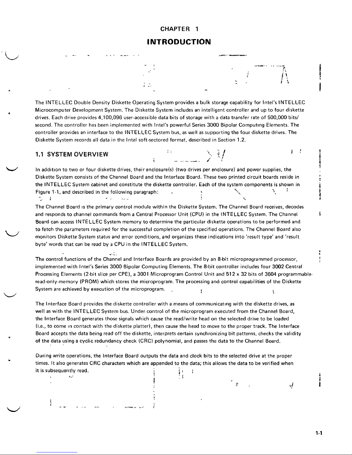
In
addition
to two or
four
diskette drives,
their
enclosure(s)
(two drives
per
enclosure)
and
power supplies,
the
Diskette System
consists
of the
Channel Board
and the
Interface Board. These
two
printed
circuit
boards
reside
in
the
INTELLEC
System cabinet
and
constitute
the
diskette controller. Each
of the
system components
is
shown
in
\
t
-9
.
,3
.
.,
...
...~
.~,.~
3,
g.-,
-
^
\
J
1,
i
*
5
The
Channel Board
is
the
primary
control
module
within
the
Diskette System.
The
Channel Board
receives,
decodes
and
responds
to
channel commands
from a Central
Processor
Unit
(CPU)
in the
INTELLEC
System.
The
Channel
Board
can
access
INTELLEC
System
memory
to
determine
the
particular
diskette
operations
to be
performed
and
to
fetch
the
parameters required
for the
successful
completion
of the
specified operations.
The
Channel Board
also
monitors
Diskette System status
and
error
conditions,
and
organizes
these indications
into
'result
type'
and
'result
byte'
words
that
can be
read
by a CPU in the
INTELLEC
System.
*
«•'
-i
,
The
control
functions
of the
Channel
and
Interface Boards
are
provided
by an
8-bit
microprogrammed processor,
implemented
with
Intel's
Series
3000
Bipolar
Computing
Elements.
The
8-bit
controller
includes
four
3002
Central
Processing
Elements (2-bit
slice
per
CPE), a 3001 Microprogram
Control
Unit
and
512
x 32
bits
of
3604
programmable-
read-only-memory
(PROM)
which
stores
the
microprogram.
The
processing
and
control
capabilities
of the
Diskette
System
are
achieved
by
execution
of the
microprogram.
,
r
The
Interface Board provides
the
diskette controller
with a means
of
communicating
with
the
diskette drives,
as
well
as
with
the
INTELLEC
System bus.
Under
control
of the
microprogram
executed
from
the
Channel
Board,
the
Interface Board
generates
those
signals
which
cause
the
read/write head
on the
selected drive
to be
loaded
(i.e.,
to
come
in
contact
with
the
diskette
platter),
then
cause
the
head
to
move
to the
proper track.
The
Interface
Board accepts
the
data being
read
off the
diskette, interprets certain synchronizing
bit
patterns, checks
the
validity
of the
data using a cyclic
redundancy
check (CRC)
polynomial,
and
passes
the
data
to the
Channel Board.
During
write
operations,
the
Interface Board
outputs
the
data
and
clock bits
to the
selected drive
at the
proper
times.
It
also
generates
CRC
characters
which
are
appended
to the
data; this allows
the
data
to be
verified when
it is
subsequently
read.
j
i * S
1-1
Page 10
cc
(D
o
3
00
s
UJ
CO
CO
LLJ
f-
UJ
V)
Q
0)
3
O)
1-2
Page 11
When
the
diskette
controller
requires
access
to
INTELLEC
System
memory,
the
Interface Board requests
and
maintains
master
control
of the
system bus,
and
generates
the
appropriate memory command.
When
a CPU in the
INTELLEC
System
issues a channel command
to the
Diskette System,
the
Interface Board
acknowledges
the
command
as
required
by
INTELLEC System
bus
protocol.
Each
diskette drive consists
of
read/write
and
control
electronics
(on a
single
printed
circuit
board), drive
mechanism,
read/write head, track positioning mechanism
and the
removable
diskette platter.
These
compo-
nents
interact
to
perform
the
following
functions:
•
Interpret
and
generate
control
signals.
•
Move read/write head
to
selected
track.
*
"r
•
Read
and
write
data.
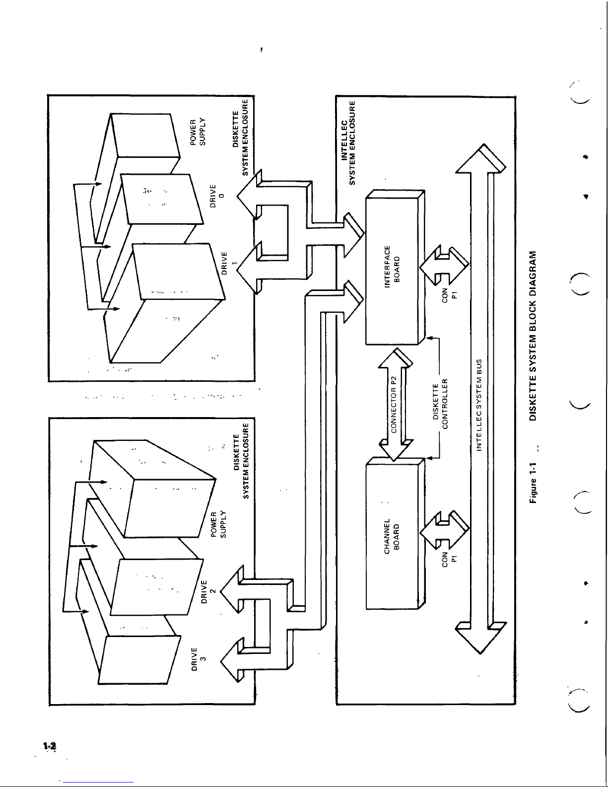
Table
1-1
lists
the
performance
characteristics
for
each
diskette drive.
TABLE
1-1
DISKETTE DRIVE PERFORMANCE SPECIFICATIONS
Capacity
(formatted)
Data
Transfer Rate:
Access
Time:
Average
Access
Time:
Rotational Speed:
Average
Latency:
Recording
Mode:
Per
Disk
-
Per
Track
-
Track
to
Track
-
Settling Time
—
512,512 bytes
6,656
bytes
500
kilobits/second
10
ms
10 ms
260 ms
360 RPM
83 ms
(M^FM)
Modified-Modified
Frequency Modulation
The
remaining chapters
of the
manual deal
with
each
of the
system
elements
in
detail. Chapter 2 describes
the
range
of
operations
that
can be
performed
by the
Diskette System,
and
also
provides specific information
on
how to
program
the
system
to
execute
each
of the
possible operations. Chapters
3 and 4
provide detailed
information
on the
theory
of
operation
for the
Channel Board
and the
Interface
Board,
respectively.
The
final
section
in
each
of
these
chapters provides a complete schematic drawing
of the
board
as
well
as a
detailed
pin
list.
The
reader should continually refer
to
these schematic drawings
in the
course
of
reading
the
theory
of
operation sections.
1-3
Page 12
NOTE:
To
avoid
any
confusion when referring
to the
schematics
for the
Channel
and
Interface
Boards,
or
when
reading
the
corresponding
circuit
descriptions,
the
following
notation,
concerning
the
active level
of a
signal,
will
apply:
Whenever a signal
is
active-low,
its
mnemonic
is
followed
by a
slash;
for
example
MRDC/
means
that
the
level
on
that
line
will
be low
when
the
memory
read
command
is
true (active).
If the
signal
is
subsequently inverted, thus making
it
active-high,
the
slash
is
omitted;
for
example,
MRDC
means
that
the
level
on
that
line will
be
high when
the
memory command
is
true.
Chapter 5 lists
the
manufacturer's
information
on the
diskette
drives.
Chapter 6 provides
the
major state
flow
charts
for the
microprogram
which
is
executed
by the
Series
3000
Bipolar
Microcomputer
Set (on the
Channel
Board),
and
which
essentially controls operation
of the
Diskette System. Chapter 7 provides basic
information
on the
installation
and use of the
Diskette System.
Finally,
Chapter 8 summarizes
the AC and DC
operating
characteristics
for the
Diskette System.
Before proceeding
to
Chapter
2,
however,
we
first provide a comprehensive review
of the
Intel
soft-sectored
recording
format
which
is
used
by the
Diskette Operating System.
1.2
RECORDING FORMAT
This section summarizes
the
specifications
for the
soft-sectored recording
format
used
by the
Diskette Operating
System.
->«•;- !«-»
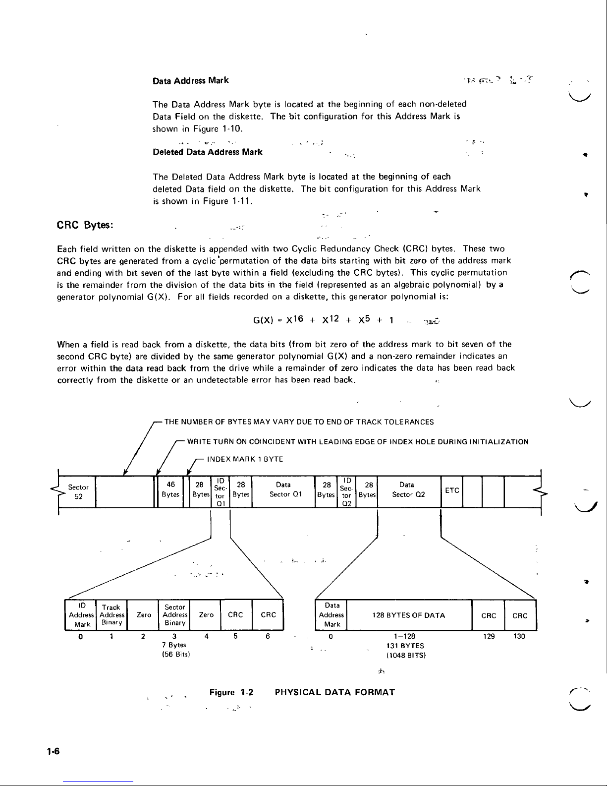
Physical
Data
Format:
The
physical data
format
is the
format
that
the
diskette
controller
circuitry
must interact
with.
The
elements
of the
physical data
format
are the
hard index hole, index mark, sector
address
marks, sector
headers,
and
data
sectors.
The
index mark
and
sector
address
marks
are
recorded
with
unique
clock patterns requiring
the
con-
troller
circuitry
to
accumulate
the
unique
clock
patterns
for
index
and
sector
address
mark
identification.
Figure
1-2
illustrates
the
general physical data
format.
J
.<
*• ;-.Y
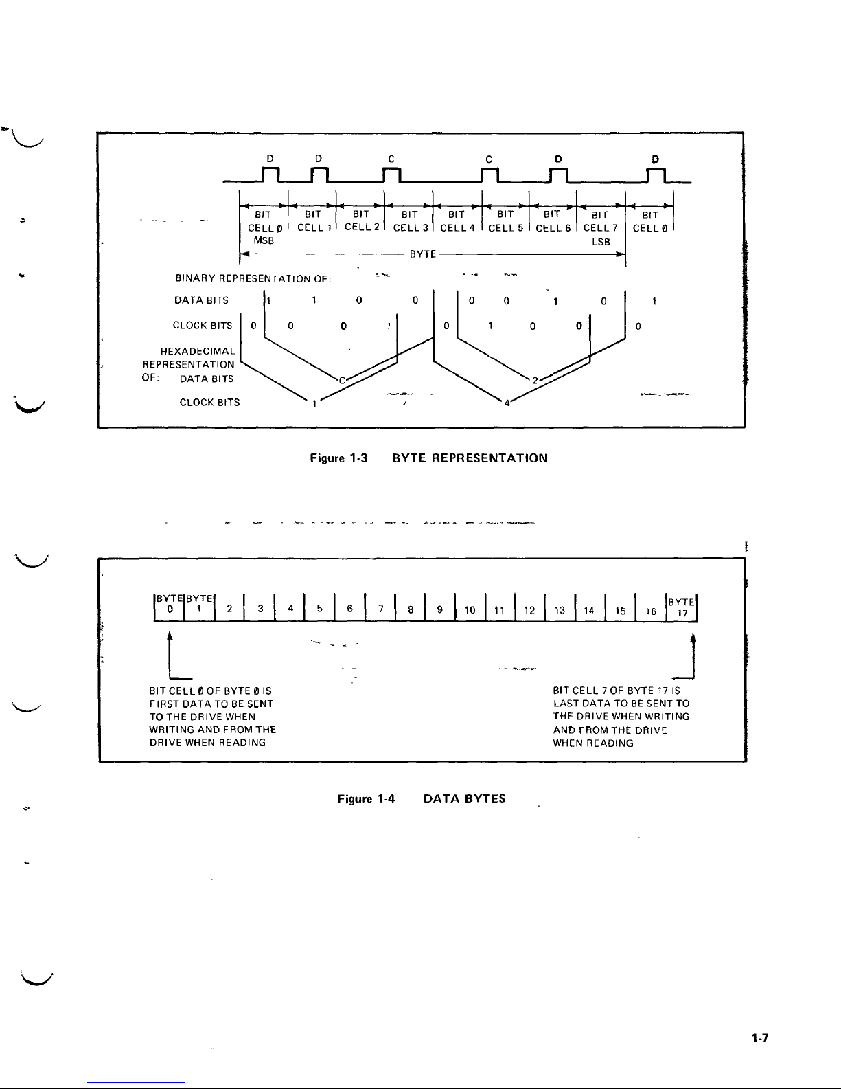
A
'byte',
when referring
to
serial
data (being
written
to or
read
from
the
diskette drive),
is
defined
as
eight
(8)
consecutive
bit
cells.
The
most
significant
bit
cell
is
defined
as bit
cell
0 and the
least
significant
bit
cell
is
defined
as bit
cell
7.
When reference
is
made
to a
specific data
bit
(i.e., data
bit 3), it is
with
respect
to the
corresponding
bit
cell (bit cell
3).
During a write
operation
bit
cell
0 of
each
byte
is
transferred
to the
drive
first
with
bit
cell 7 being
transferred
last.
Correspondingly,
the
most significant
byte
of
data
is
transferred
to the
diskette first
and the
least
signifi-
cant
byte
is
transferred last.
When data
is
being read back
from
the
drive,
bit
cell
0 of
each
byte
will
be
transferred first
with
bit
cell
7
last.
As
with
reading,
the
most significant
byte
will
be
transferred first
from
the
drive
to the
user.
Figure
1-3
illustrates
the
relationship
of the
bits
within a byte
and
Figure
1-4
illustrates
the
relationship
of the
bytes
for
read
and
write
data.
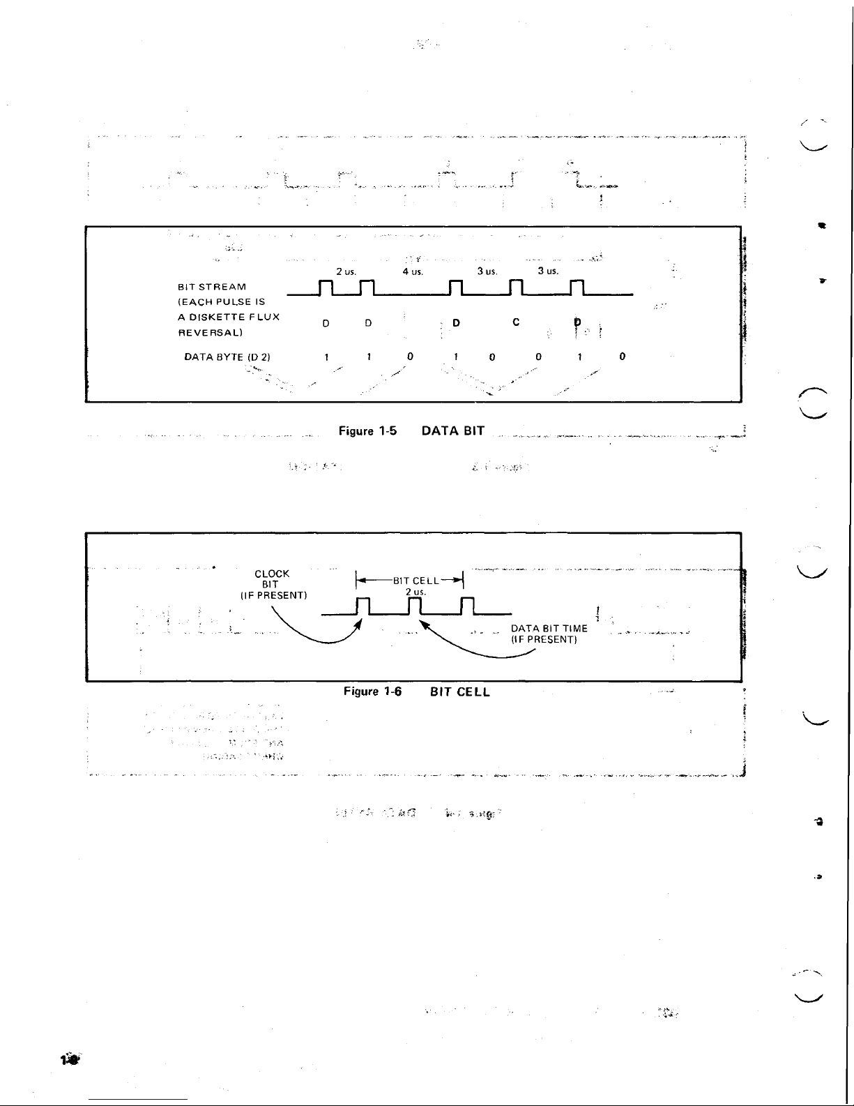
Data
is
recorded
on the
diskette using
modified
modified
(M^)
frequency
modulation
as the
recording mode. Data
written
on and
read back
from
the
disc takes
the
form
shown
in
Figure
1-5.
Clock bits
are
written
only
if
there
is
no
data
bit in the bit
cell
and
there
was no
data
bit or
clock
bit
written
in the
previous
bit
cell.
By
definition,
a
Bit
Cell
is the
period
(2 us)
consisting
of a
clock
bit
time
(1 us) and a
data
bit
time
(1
us). Figure
1-6
illustrates
a
Bit
Cell.
1-4
Page 13
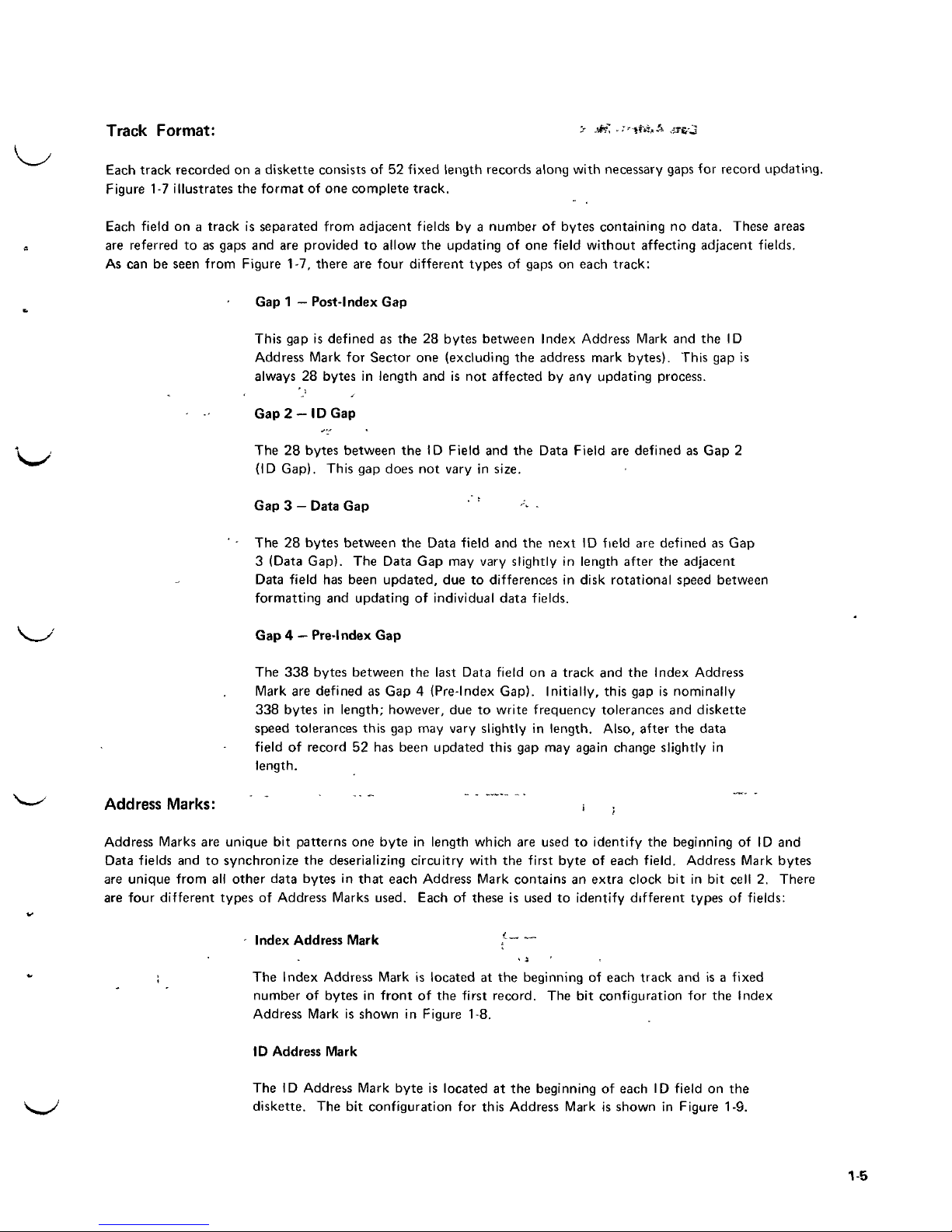
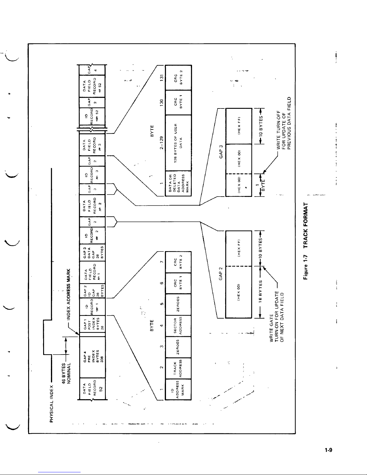
Track
Format:
>
•*' • •*••-»**«**
w3
Each
track recorded
on a
diskette consists
of 52
fixed length records along
with
necessary
gaps
for
record updating.
Figure
1-7
illustrates
the
format
of one
complete track.
Each
field
on a
track
is
separated
from adjacent
fields
by a
number
of
bytes containing
no
data.
These
areas
c
are
referred
to as
gaps
and are
provided
to
allow
the
updating
of one
field
without
affecting adjacent fields.
As
can be
seen
from
Figure 1-7, there
are
four
different types
of
gaps
on
each
track:
Gap 1 —
Post-Index
Gap
This
gap is
defined
as the 28
bytes
between Index
Address
Mark
and the ID
Address
Mark
for
Sector
one
(excluding
the
address
mark bytes). This
gap is
always
28
bytes
in
length
and is not
affected
by any
updating
process.
'
-r j/
Gap
2-ID
Gap
^..r
t
t
,
The 28
bytes between
the ID
Field
and the
Data Field
are
defined
as Gap 2
(ID
Gap). This
gap
does
not
vary
in
size.
Gap
3 -
Data
Gap
' - The 28
bytes between
the
Data
field
and the
next
ID
field
are
defined
as Gap
3
(Data Gap).
The
Data
Gap may
vary
slightly
in
length after
the
adjacent
Data
field
has
been updated,
due to
differences
in
disk rotational
speed
between
formatting
and
updating
of
individual
data
fields.
V / Gap 4 — Pre-lndex
Gap
The 338
bytes between
the
last
Data field
on a
track
and the
Index
Address
Mark
are
defined
as Gap 4
(Pre-lndex
Gap).
Initially,
this
gap is
nominally
338
bytes
in
length; however,
due to
write frequency
tolerances
and
diskette
speed
tolerances this
gap may
vary slightly
in
length.
Also,
after
the
data
field
of
record
52 has
been
updated this
gap may
again
change
slightly
in
length.
NS
---^
Address
Marks:
\
,
Address
Marks
are
unique
bit
patterns
one
byte
in
length which
are
used
to
identify
the
beginning
of ID and
Data
fields
and to
synchronize
the
deserializing
circuitry
with
the
first byte
of
each
field.
Address
Mark bytes
are
unique
from
all
other data bytes
in
that
each
Address
Mark contains
an
extra clock
bit in bit
cell
2.
There
are
four
different types
of
Address
Marks
used.
Each
of
these
is
used
to
identify
different types
of
fields:
%**
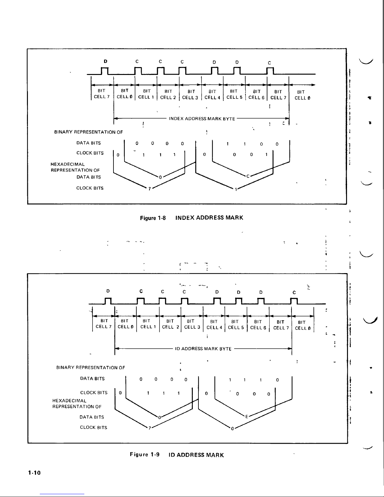
Index
Address
Mark
'r—"
>
i
;
The
Index Address Mark
is
located
at the
beginning
of
each track
and is a
fixed
number
of
bytes
in
front
of the
first record.
The bit
configuration
for the
Index
Address
Mark
is
shown
in
Figure 1-8.
ID
Address
Mark
The ID
Address
Mark byte
is
located
at the
beginning
of
each
ID
field
on the
diskette.
The bit
configuration
for
this
Address
Mark
is
shown
in
Figure 1-9.
1-5
Page 14
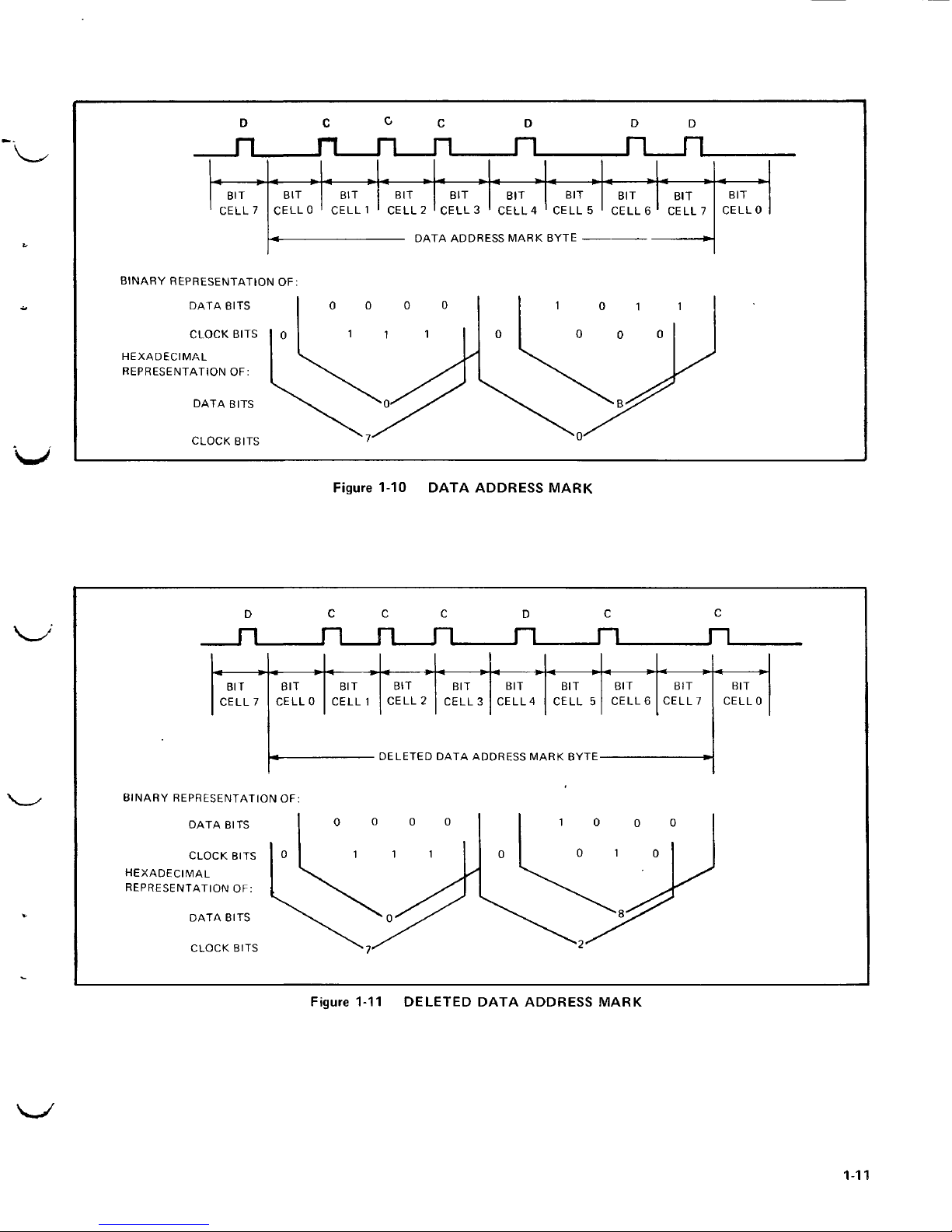
Data
Address
Mark
The
Data Address Mark byte
is
located
at the
beginning
of
each
non-deleted
Data
Field
on the
diskette.
The bit
configuration
for
this Address Mark
is
shown
in
Figure 1-10.
'•*
- ~ V
,-' *
" " •_ * r
-_
<
Deleted Data
Address
Mark
.
CRC
Bytes:
The
Deleted Data
Address
Mark byte
is
located
at the
beginning
of
each
deleted
Data field
on the
diskette.
The bit
configuration
for
this
Address
Mark
is
shown
in
Figure
1-11.
Each
field
written
on the
diskette
is
appended
with
two
Cyclic Redundancy Check (CRC) bytes.
These
two
CRC
bytes
are
generated
from a cyclic'permutation
of the
data bits starting
with
bit
zero
of the
address
mark
and
ending
with
bit
seven
of the
last
byte
within a field (excluding
the CRC
bytes). This cyclic permutation
is
the
remainder
from
the
division
of the
data bits
in the
field (represented
as an
algebraic
polynomial)
by a
generator
polynomial G(X).
For all
fields recorded
on a
diskette, this generator polynomial
is:
t~*
I
\y
\
\/1R
i
V 1
*?
i
V R
i
-1
—
b(X) - XID +
X1^ + X° + 1
75.x,-
When a field
is
read
back
from a diskette,
the
data
bits
(from
bit
zero
of the
address
mark
to bit
seven
of the
second
CRC
byte)
are
divided
by the
same
generator polynomial G(X)
and a
non-zero remainder indicates
an
error
within
the
data
read
back
from
the
drive while a remainder
of
zero indicates
the
data
has
been
read
back
correctly
from
the
diskette
or an
undetectable error
has
been
read
back.
THE
NUMBER
OF
BYTES
MAY
VARY
DUE TO END OF
TRACK TOLERANCES
/—
WRITE
TURN
ON
COINCIDENT
WITH
LEADING
EDGE
OF
INDEX HOLE
DURING
INITIALIZATION
/
'
Sector
r
*
/
/
IINUtA
MAKrx \ BY 1 t
/ /
46
Bytes
28
Bytes
ID
Sec-
tor
Q1
28
Bytes
Data
Sector
Q1
28
Bytes
ID
Sec-
tor
Q2
28
Bytes
Data
Sector
Q2
ETC
J
ID
Address
Mark
Track
Address
Binary
Zero
Sector
Address
Binary
Zero
CRC
CRC
0123456
7
Bytes
(56
Bits)
Data
Address
Mark
128
BYTES
OF
DATA
CRC
CRC
0
1-128
129 130
131
BYTES
(1048 BITS)
'f;
Figure
1-2
PHYSICAL
DATA
FORMAT
1-6
Page 15
c
n.
D
n
BIT
CELLO
MSB
BIT
CELL
1
BIT
CELL
2
BIT
CELLS
nw-rr
BIT
CELL4
BIT
CELL
5
BIT
CELL
6
BIT
CELL
7
LSB
BIT
CELLD
BINARY REPRESENTATION
OF:
DATA
BITS
CLOCK BITS
HEXADECIMAL
REPRESENTATION
OF:
DATA
BITS
CLOCK
BITS
Figure
1-3
BYTE REPRESENTATION
I
BYTE
0
BYTE
1
2
3
4
5
6
7
| 8
9
10
11
12
13
I 14
15
16
BYTE
17
BIT
CELL
OOF
BYTE
0 IS
FIRST
DATA
TO BE
SENT
TO
THE
DRIVE WHEN
WRITING
AND
FROM
THE
DRIVE
WHEN READING
BIT
CELL 7 OF
BYTE
17 IS
LAST DATA
TO BE
SENT
TO
THE
DRIVE WHEN WRITING
AND
FROM
THE
DRIVE
WHEN
READING
Figure
1-4
DATA
BYTES
1-7
Page 16
•.;:_^
2 us.
BITSTREAM
p~|
p~|
(EACH
PULSE
IS
A
DISKETTE FLUX
REVERSAL)
DATA
BYTE
(D 2) 1 1
..'*•'->
.-••'
""".'-•••.. , X
. - '
"
.. ^ -
4 us. 3 us. 3 us.
n
n n
D C D
010010
"
.,
.
-•
'
-•
V-,*'
Figure
1-5
DATA
BIT
CLOCK
BIT
(IF
PRESENT)
-BITCELL—*•]
2
us.
J1
TL
DATA
BIT
TIME
(IF
PRESENT)
Figure
1-6 BIT
CELL
1-8
Page 17
MARK
UI
cc
a
Q
X
01
Q
46
BYTES
NOMINAL
X
UJ
Q
a/
<
O
<
u
D
LL
UJ
a.
< N
O
< Q cc
t m °
^
-
U
Q
u.
UJ
I
<
O
D
OC
n
Q
0
- U JJ
a.
<
O
< Q
oc
K
-1 0
N
< * U
„
Q
u.
UJ
«
CC
Q.
<
O
Q
DC
Q
g
—
U
UJ
CC
"
<
a.
(-
a.
i-
< < <
oo
>
O
Q O Si a
a
u.
oc
o.
a.
(_
< Q <
a)
>
0 2 0 8
m
Q
oc
D
0
- u
UJ
CC
X CO
r
»-
uj uj
°:
(0 D
K
< O z >
en
0 tt. £
CD
S
<
1^ D V
«
< X -r
> n
(3
a. = m
n
Q
< Q
DC
1-
-J
O
<
uj
u
LU
I-
CQ
o
n
CM
CN
-
CN
O
ui
OC
H
(J
>-
CO
U
ui
CC
H
u
>
CO
cc
UJ
D
u.
°
*
H
°
m
CO
CN
CC
Q
</)
o
£
[S
< S <
cc
^
1-
-1
1-
Q CC
<
UJ
< Q <
Q
Q Q <
5
m
r-.
t£>
in
•"3-
„
CM
•-
CN
U
IU
CC
1-
u
>
m
CJ
UJ
CC
H-
u
>
CO
en
UJ
O
a.
N
rr
<"
CC
CO
O
ui
1-
CC
0 Q
UI
Q
<f>
<
en
UJ
O
cc
UI
N
^
en
ej
uj
tt
Q
L_
Q
en
UJ
*
9 S <
Q
2
X
UJ
I
O
o
o
o
X
UJ
X
cc
O
u.
*
O
<
oc
cu
>_
3
a;
O
oo
I
a.
1-9
Page 18
D
D
_n_
BIT
CELL?
BIT
CELLO
n
i
BIT
CELL
1
n
BIT
CELL2
\
•
i M nr
n
n n
BIT
CELLS
BIT
CELL4
».
.X
ADDRESS
MARK
BIT
CELL
5
BIT
CELL
6
n
BIT
CELL?
B T TE
^
BIT
CELLO
BINARY
REPRESENTATION
OF
DATA
BITS
CLOCK BITS
HEXADECIMAL
REPRESENTATION
OF
DATA
BITS
CLOCK BITS
0000
1100
Figure
1-8
INDEX
ADDRESS MARK
BIT
CELL?
-5
BIT
CELLO
BIT
CELL
1
BIT
CELL
2
BIT
CELL
3
A
rvrvD
ccc*
BIT
CELL4
BIT
CELL
5
BIT
CELL
6
BIT
CELL?
1 U AAL/LMll-OO
IVIMMIS.
L> 1 1
L.
^
BIT
CELLO
BINARY
REPRESENTATION
OF
DATA
BITS
CLOCK
BITS
HEXADECIMAL
REPRESENTATION
OF
DATA BITS
CLOCK
BITS
0000
1110
Figure
1-9 ID
ADDRESS
MARK
1-10
Page 19
D
D
D
_TL
BIT
CELL?
BIT
CELLO
n
i
BIT
CELL
1
BIT
CELL
2
rv
AH
n
n n n
BIT
CELLS
"A
ADORE
BIT
CELL4
SS
MARK
BIT
CELL
5
RYTE
BIT
CELL
6
BIT
CELL?
BIT
CELLO
BINARY
REPRESENTATION
OF
DATA BITS
CLOCK BITS
HEXADECIMAL
REPRESENTATION
OF:
DATA
BITS
CLOCK BITS
1011
Figure
1-10
DATA
ADDRESS
MARK
D
C C
n
TL
C
n
D
n
C
n
C
J~L
BIT
CELL
7
BIT
CELLO
BIT
CELL
1
—
BIT
CELL
2
BIT
CELL
3
BIT
CELL4
BIT
CELL
5
DELETED
DATA
ADDRESS
MARK BYTE-
BIT
CELL6
BIT
CELL?
BIT
CELLO
BINARY
REPRESENTATION
OF
DATA BITS
CLOCK BITS
HEXADECIMAL
REPRESENTATION
OF:
DATA BITS
CLOCK
BITS
1000
Figure
1-11
DELETED
DATA
ADDRESS
MARK
1-11
Page 20

LL-L
>iaviA!
ssaaoov
viva
0313130
LI-I
0 0 0
L
0000
sna
M3O13
sii9
viva
:
dO
NOIlVlN3S3Hd3y
1VIAII330VX3H
S1I9
X3013
sim
viva
dO
NOIlVlN3S3Hd3d
AHVNI9
01133
119
£ii33
119
91133
119
•31A9
XdVIAI
SS3HQaV
VIVO
031313C
9
H130
119
t-1130
119
€1130
119
2
1130
119
*•
L
1133
119
01133
119
^1130
119
LJ
3
LJ
0
LJ
a
LJ
3
U
LT
3 3
>iaVIAI
SS3HOOV
VIVO
OL-L
3jnB
!d
L
L 0 L
S1I9
»3O13
sim
viva
•dO
NOIlVlN3S3Hd3d
1VIAII330VX3H
S1I9
>I3013
siig
viva
dO
NOIlVlN3S3dd3y
AHVNI9
01133
119
Z.1133
119
91133
119
n_i-Aa
9
1133
119
»HVIAISS'
1^1133
119
gaaav
vj
£
1133
119
LJ
U U U
21130
118
I
1133
119
LJ
01133
119
Z.1133
119
U
a
a
a
Page 21
CHAPTER
2
OPERATIONAL
SUMMARY
AND
PROGRAMMING
CONSIDERATIONS
All
diskette operations
are
initiated
by a
Central
Processor
Unit
(CPU)
within
the
INTELLEC
System. Once
initiated,
however,
the
Diskette Channel completes
the
specified operation
without
further
intervention
on the
part
of the
CPU. From
the
CPU's
point
of
view, there
are
only
three general
steps
required
to
complete
any
diskette operation:
• The CPU
must prepare
and
store
in
system memory
an I/O
Parameter Block (IOPB)
for
each
operation
to be
performed.
An
IOPB
(seven
bytes)
specifies a particular
diskette operation
and
provides
all of the
parameters required
for
execution
of
that
operation.
• The CPU
must
then
pass
the
memory
address
of the
IOPB
to the
Diskette Channel.
• The CPU
must
process
the
result
information
from
the
Diskette Channel
upon
completion
of the
operation(s).
The
preparation
of the
IOPB
by the
CPU,
in
itself, requires
no
interaction
with
the
Diskette Channel.
The
passing
of the
memory
address
for the
IOPB
and the
result processing, however,
do
require interaction.
Six
channel com-
mands
have
been defined
to
allow
the CPU to
perform these interactive
steps.
Three
of the
channel commands
are
the
result
of the CPU
executing
an
output
instruction
to a
dedicated
I/O
port
address,
while
the
other three
commands
are the
result
of
input
instructions
to
dedicated ports.
The six
channel commands are:
(1)
Write memory
address
lower
(output)
(2)
Write memory
address
upper
and
start
the
diskette operation
(output)
(3)
Reset
the
channel
(output)
(4)
Read
subsystem status
(input)
(5)
Read
result
type
(input)
(6)
Read
result
byte
(input)
••-->•
The CPU
outputs
the
memory
address
of the
IOPB
by
executing channel commands
1 and 2.
Upon
execution
of
channel command
2, the
Diskette Channel
will
request master
control
of the
INTELLEC System bus, fetch
the
diskette
instruction
and
associated
parameters
from
the
IOPB,
and
proceed
to
perform
the
specified diskette
operation.
The
diskette
instruction
byte
in the
IOPB
can
specify
any one of
seven
diskette operations:
(1)
Recalibrate
(seek
track
00)
(2)
Seek
(3)
Format a track
(4)
Write data
(with
data
address
marks)
(5)
Write data
(with
deleted
address
marks)
(6)
Read
data
(7)
Verify
CRC
The
Diskette Channel
can
interrupt
the CPU
when
the
operation
is
completed
or
when
the
diskette ready status
changes.
The
host
system software
can
implement
its CPU
interrupt
mechanism
via
this
direct
interrupt
feature
or it can
'poll'
the
Diskette Channel
by
executing channel command 4 (read
subsystem status). When
the CPU
determines
that
the
operation sequence
has
beer completed (either
by
receiving
an
interrupt
request
or by
reading
2-1
Page 22
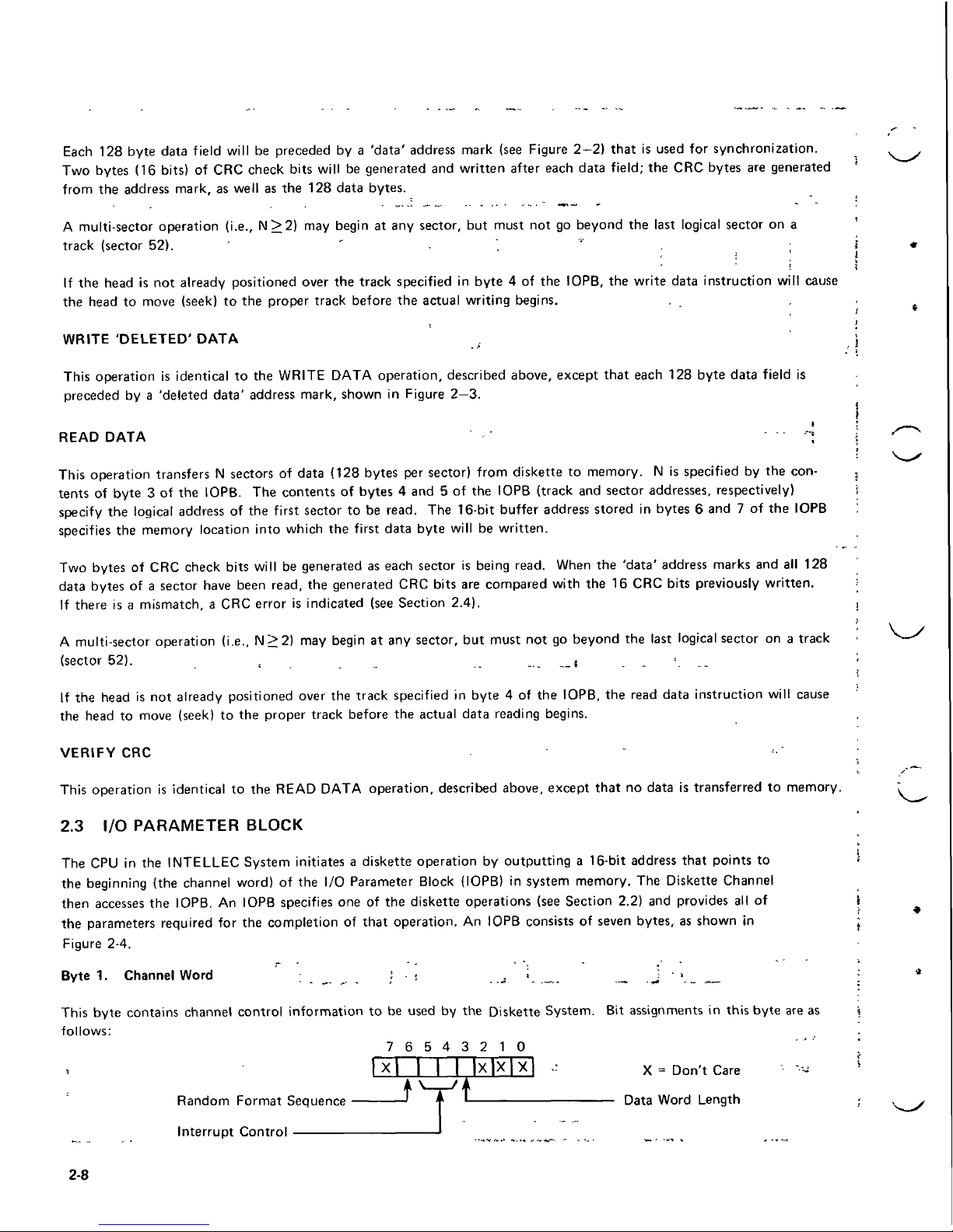
FORMAT
TRACK
"
:•*-.--
K- - -
This
operation initializes
the
track
specified
in
byte
4 of the
IOPB,
by
writing
all
address
marks,
gaps,
address
fields
and
data fields,
as
shown
in
Figure
2—1.
The
various address marks
and
fields
are
defined
in
Section 1.2.
The
method
of
assigning logical sector
addresses,
which
are
written
into
the
sector
address
fields,
is
specified
by bit 6
of the
first IOPB
byte
(the channel word).
If
this
bit is
equal
to
logical
0 the
sequence
of
logical sector
addresses
will
match
the
physical sequence
on the
diskette (i.e., sector
address
'01'
is
written
into
the
first physical sector after
the
index
mark,
sector
address
'02'
is
written
into
the
second physical sector,
and so
on).
In
addition,
the
data
byte
stored
in the
memory location specified
by the
16-bit
buffer
address
contained
in
bytes
6 and 7 of the
IOPB
will
be
written
into
the
128-byte
locations
of
each sector's data
field.
No
other
data bytes need
to be
stored
in
this
buffer.
If, on the
other
hand,
the
sequence
of
logical
addresses
being
assigned
to the
sectors
is
'random'
(that
is, do not
match
the
physical sequence
of
sectors),
bit 6 of the
channel
word
will
be
equal
to
logical
1, and 104
bytes
(52
pairs)
of
data
will
be
stored
in
memory beginning
at the
16-bit
buffer
address contained
in
bytes
6 and 7 of the
IOPB. Each
of the
52
pairs
of
data bytes
will
specify
the
logical sector
address
to be
written
into
the
sector
address
field
of the
corres-
ponding
physical sector,
and the
data character
which
will
be
written
(128 times)
into
the
data
field
portion
of
that
sector.
For
example,
if the
fiist
four
bytes
of the
buffer are:
Byte Contents (hex)
1
01
2
FF
3
oe
4
00
Then,
sector
address
'01'
will
be
written
into
the
sector address
field
of the
first
physical sector after
the
index
mark,
and
'FF-jg'
(all ones)
will
be
written
into
each
of the 128
byte
locations
in the
data field
portion
of
this sector.
The
sector
address
'OE-jg'
(14-^Q)
W|
'H
be
written
into
the
sector
address
field
of the
second physical sector (i.e.,
the
sector
which
is
physically next
to the
first
sector),
and
'00-|g'
(all
zeros)
will
be
written
into
each
of the 128
byte
locations
in the
data
field
portion
of
this sector.
And so on,
until a logical sector
address
has
been
written
into
the
sector
address
field
of
each
of the 52
physical
sectors
on the
track,
and a
data byte
is
written
into
each
of the 128
byte
locations
in the
data field
portion
of
each
of the 52
sectors.
The
firmware
implementation
of the
format
command
is
such
that
in
order
to
format
track n (n^0),
track
n-1
must
already
be
formatted (i.e., already
have
readable
address
information
written
into
it). Track
0 can
always
be
formatted
even
if no
valid
address
information
is
written
on the
disk.
During
formatting, a 'data
mark'
(i.e., a character
which
has a
clock
pattern
equal
to
70-|g
and a
data
pattern
equal
to
OB-|g;
see
Figure
2—2)
is
written
into
the
'data/deleted
data
address
marl ' character
position
of
each sector (i.e.,
the
character
position immediately preceding
the 128
byte
date field.)
If,
when
the
format
track operation
is
initiated,
the
head
is not
already positioned over
the
track specified
in
byte
4 of
the
IOPB,
the
format
track
instruction
will
cause
the
head
to
move
(seek)
to the
proper
track
before
the
actual for-
matting
begins.
"
"
"
WRITE
DATA
This operation transfers
N x 1 28
bytes
of
contiguous data
from
memory
to the
diskette. N represents
the
number
of
sectors
to be
written.
N is
specified
by the
contents
of
byte
3 of the
IOPB.
The
16-bit
buffer
address
stored
in
bytes
6 and 7 of the
IOPB specifies
the
memory
location
containing
the
first data
byte
to be
transferred.
The
contents
of
bytes
4 and 5 of the
IOPB (track
and
sector
addresses,
respectively) specify
the
logical address
of the
first
sector
to
be
written
into.
2-6
Page 23
executed
sequentially
('read
result
type'
first),
and
should
be
executed
only
in
response
to an
interrupt
request
from
the
Diskette Channel; execution
at
other times could produce erroneous result data.
The use and
format
of
each
of the six
channel commands
is
described below:
WRITE
MEMORY
ADDRESS LOWER
(OUTPUT)
-
- .
This channel command
outputs
the low
order
byte
of the
16-bit
memory
address
that
points
to
byte 1 ('channel
word')
of
the
IOPB.
,.. _ _
_.
System
address
bus: BASE
+ 1
\
System data bus: Eight
least
significant
bits
of the
16-bit
memory
address
that
points
to the
first
IOPB.
WRITE
MEMORY
ADDRESS UPPER
AND
START
THE
DISKETTE
OPERATION
(OUTPUT)
This channel command
outputs
the
high order
byte
of the
16-bit
memory
address
that
points
to
byte
1 of the
IOPB.
This command
also
causes
the
Diskette Channel
to
begin executing
the
diskette operation specified
in
byte 2 (instruction
byte)
of the
addressed
IOPB.
System
address
bus: BASE
+ 2
System data bus: Eight most significant bits
of the
16-bit
memory
address
.
.
,
RESET
DISKETTE
SYSTEM
(OUTPUT)
This
output
channel command
causes
all
control
logic
in the
Diskette Channel
to be
reset
in an
initialized state.
If
this command
is
issued
while a 'write
data'
diskette operation
is in
progress,
the
data
in the
sector
currently
being
written
will
be
garbled. This command
is
intended
to
clear a 'hang
up'
in the
Diskette Channel.
System
address
bus: , BASE
+ 7
System
data bus:
Not
used.
$•
+
READ
SUBSYSTEM
STATUS
(INPUT)
This
input
channel command
causes
the
Diskette Channel
to
return.
bit
0 -
ready status
of
drive
0
bit 1 —
ready
status
of
drive
1
bit 2 —
state
of the
channel's
interrupt
flip-flop
bit 3 —
controller
presence
indicator
bit 4 —
double density controller
presence
indicator
bit 5 —
ready status
of
drive
2
bit 6 —
ready status
of
drive
3
2-3
Page 24
Each
128
byte data field
will
be
preceded
by a
'data'
address
mark (see Figure 2-2)
that
is
used
for
synchronization.
^^
Two
bytes
(16
bits)
of CRC
check bits
will
be
generated
and
written
after each data
field;
the CRC
bytes
are
generated
from
the
address
mark,
as
well
as the 128
data bytes.
A
multi-sector operation (i.e.,
N>2)
may
begin
at any
sector,
but
must
not go
beyond
the
last logical sector
on a
track (sector 52).
"
"
. ;
I
«
1
1
If the
head
is not
already
positioned
over
the
track
specified
in
byte
4 of the
IOPB,
the
write
data
instruction
will
cause
the
head
to
move
(seek)
to the
proper track before
the
actual
writing
begins.
. ,
/
*
}
WRITE
'DELETED'DATA
i
.
j-
/
5
This operation
is
identical
to the
WRITE
DATA
operation, described above, except
that
each
128
byte
data
field
is
preceded
by a
'deleted
data'
address
mark,
shown
in
Figure
2—3.
.
a
_^
READ
DATA
1
j
^^
This operation
transfers N sectors
of
data (128 bytes
per
sector)
from
diskette
to
memory.
N is
specified
by the
con-
?
tents
of
byte
3 of the
IOPB.
The
contents
of
bytes
4 and 5 of the
IOPB
(track
and
sector addresses, respectively)
j
specify
the
logical
address
of the
first
sector
to be
read.
The
16-bit
buffer
address
stored
in
bytes
6 and 7 of the
IOPB
:
specifies
the
memory location
into
which
the
first data
byte
will
be
written.
Two
bytes
of CRC
check bits
will
be
generated
as
each
sector
is
being read. When
the
'data'
address
marks
and all 128
data bytes
of a
sector
have
been read,
the
generated
CRC
bits
are
compared
with
the 16 CRC
bits
previously
written.
;
If
there
is a
mismatch,
a CRC
error
is
indicated (see Section 2.4).
s
A
multi-sector operation (i.e.,
N>2)
may
begin
at any
sector,
but
must
not go
beyond
the
last logical sector
on a
track
-
—
(sector
52).
(
_
{
_.'._.
If the
head
is not
already
positioned
over
the
track specified
in
byte
4 of the
IOPB,
the
read
data
instruction
will
cause
the
head
to
move
(seek)
to the
proper track before
the
actual data reading begins.
VERIFY
CRC
This operation
is
identical
to the
READ
DATA
operation,
described above, except
that
no
data
is
transferred
to
memory.
:
2.3 I/O
PARAMETER
BLOCK
The CPU in the
INTELLEC
System initiates a diskette
operation
by
outputting a 16-bit
address
that
points
to *
the
beginning (the channel word)
of the I/O
Parameter
Block (IOPB)
in
system
memory.
The
Diskette Channel
then
accesses
the
IOPB.
An
IOPB
specifies
one of the
diskette operations (see Section 2.2)
and
provides
all of I
^
the
parameters required
for the
completion
of
that
operation.
An
IOPB consists
of
seven
bytes,
as
shown
in
;
Figure
2-4.
Byte
1.
Channel Word
\
-
*,
^
<
_
J
'»____
;
*
This
byte
contains channel
control
information
to be
used
by the
Diskette
System.
Bit
assignments
in
this
byte
are as
\
follows:
76543210
|X|
| | |
|X|X|X|
.:
x
=
Don't
Care
Random Format Sequence
Interrupt
Control
2-8
Data Word
Length
Page 25
If the
type
code
= 10, the
controller
has
detected a change
in the
ready status
of a
drive
and the
contents
of the
result byte
will
indicate
the
current ready
status
of the
diskette
drives:
(LSB)
76543210
Unit 1 ready
T
t( A a Reserved
Unit 0 ready
Unit 3 ready
Unit 2 ready
0
0
o[o
*
NOTE: A logical 1 means
that
the
drive
is
currently ready; a logical 0 means
the
drive
is not
ready.
It is the
responsi-
bility
of the
host system software
to
maintain appropriate tables
to
track
these
status
changes.
There
is one
instance
in
which a drive
can
appear
'not
ready'
to the
host
system,
when
in
fact
it is
ready.
For
example,
assume
that
while
drive
0 is
selected, drive 1 just
goes
not
ready then returns
to the
ready state
(perhaps
the
diskette platter
was
changed).
When
the
drive 0 operation
is
completed,
the
diskette controller
will
return
two
V J consecutive status change interrupts,
the
first
showing drive
1 not
ready,
the
second showing drive 1 ready.
The
first
interrupt,
indicating drive
1 to be not
ready,
is
returned
even
though
the
drive
is now
actually
ready
because
it is
important
that
the
operator
know
that
the
ready status
of the
drive changed while
the
other drive
was
selected.
For
instance, this
would
protect
against
inadvertently
accessing
an
'unknown'
disk,
if the
drive
went
not
ready
then
ready again because someone changed disk platters.
2.2
DISKETTE OPERATIONS
The
Diskette System
is
capable
of
performing
seven
different operations: recalibrate,
seek,
format track, write data
(with
data marks), write data
(with
deleted data marks), read data,
and
verify CRC.
To
initiate
any
diskette operation,
^—-'
the CPU
will
output
both
bytes
of the
16-bit
memory
address
that
points
to the
first byte
of an I/O
Parameter
Block
(IOPB).
The
second byte
in the
IOPB
specifies
one of the
seven
diskette operations (see Section
2.3 for
IOPB format).
After
the
Diskette System
receives
the
upper byte
of the
16-bit memory
address,
it
accesses
the
IOPB
to
determine
the
operation
to be
performed
and to
acquire
the
various
parameters
that
are
necessary
for
execution
of the
diskette instruc-
tion.
The
Diskette System
will
perform
the
specified operation, then
set its
interrupt
flip-flop.
NOTE:
The
Diskette Channel automatically unloads
the
read/write head after a fixed length
of
time
following a diskette
operation. This feature
is
meant
to
reduce head wear.
The
feature
is
implemented
by
counting
index
pulses
after a 'read
result
byte'
channel command
is
executed. When
the
specified
count
is
achieved,
the
head
is un-
loaded,
and the
count
is
re-initialized.
At
present,
the
count
is set for 6;
that
is, the
head
will
remain loaded
for at
least
five complete revolutions following
each
diskette operation
or
group
of
linked diskette operations.
The
seven
diskette operations
are
defined
in the
following paragraphs:
RECALIBRATE
?-
This operation
causes
the
head
of the
selected
diskette
unit
to be
moved over track
00. The
diskette drive's track
0
sensor
is
sampled
to
determine
successful
completion
of
this operation. This
is
often
the
first
instruction
executed
*
after a diskette
is
loaded,
or
when a seek
error occurs (see Section 2.4).
SEEK
This operation
causes
the
head
of the
selected
diskette
unit
to be
moved over
the
track specified
in
byte
4 of the
IOPB.
The
Diskette Channel
will
verify
the
head
position
by
reading
the
track
address
from
the
diskette platter before com-
pleting
the
operation.
If at the
completion
of the
head movement,
the
head
is not
over
the
expected track, a 'seek
\.
error'
will
be
indicated (see Section 2.4).
2-5
Page 26
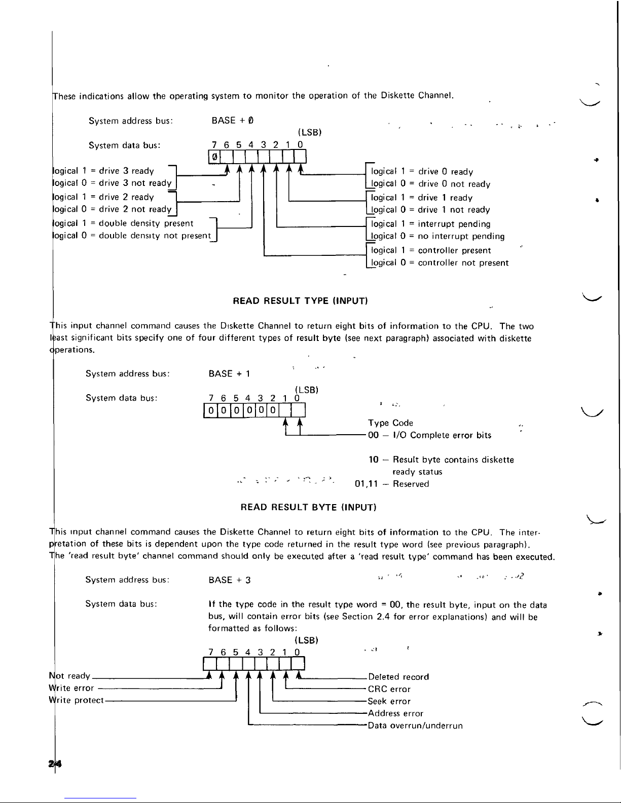
cperations.
hese
indications allow
the
operating system
to
monitor
the
operation
of the
Diskette Channel.
System
address
bus: BASE
+ 0
System data bus:
ogical
1 =
drive 3 ready
ogical
0 =
drive
3 not
ready
ogical
1 =
drive 2 ready
ogical
0 =
drive
2 not
ready
ogical
1 =
double
density present
ogical
0 =
double density
not
present
sent
t
presen
7
0
-
n
J
6
I
c
>
k
4
>
t
k
/•
>
J
k.
f
>
(LSB)
!
1 0
I
I
k A >f
logical
1 =
drive 0 ready
Jpgical
0 =
drive
0 not
ready
logical
1 =
drive 1 ready
Jpgical
0 =
drive
1 not
ready
logical
1 =
interrupt
pending
Jpgical
0 = no
interrupt
pending
logical 1 =
controller present
logical
0 =
controller
not
present
READ RESULT TYPE
(INPUT)
his
input
channel command
causes
the
Diskette Channel
to
return
eight
bits
of
information
to the
CPU.
The two
ast
significant
bits
specify
one of
four
different
types
of
result
byte
(see
next
paragraph) associated
with
diskette
BASE
+ 1
(LSB)
76543210
0
0 0
000
I
•t
System
address
bus:
System data bus:
Type
Code
00
- I/O
Complete error
bits
10 —
Result
byte
contains diskette
ready status
-"
' r ' " '•'"-'
*•
01,11 - Reserved
READ RESULT
BYTE
(INPUT)
his
input
channel command
causes
the
Diskette Channel
to
return
eight bits
of
information
to the
CPU.
The
inter-
etation
of
these
bits
is
dependent
upon
the
type
code returned
in the
result type
word
(see previous paragraph).
he
'read
result
byte'
channel
command
should
only
be
executed
after a 'read
result
type'
command
has
been
executed.
System
address
bus: BASE
+ 3
VJ
'
**
"
tf
System data bus:
If the
type
code
in the
result
type
word
- 00, the
result
byte,
input
on the
data
bus,
will
contain error bits (see Section
2.4 for
error explanations)
and
will
be
formatted
as
follows:
(LSB)
76543210
'
""'
nt
rpariy
A
>ktki
^>k
i
k A i
I
Deleted record
CRC
error
Seek
error
Address
error
Data overrun/underrun
Page 27
ID
FltLD
A
GAP
DATA
FIELD
A
GAP
V V
t t
TRACK
ADDRESS
(1
BYTE)
SECTOR
ADDRESS
(1
BYTE)
TWO
BYTES
OF CRC
CHECK
BITS
28
BYTES
'ID
1
ADDRESS
MARK
(1
BYTE)
t
128
BYTES
OF
DATA
'DATA/DELETED
DATA'
ADDRESS
MARK
(1
BYTE)
28
BYTES
TWO
BYTES
OF CRC
CHECK
BITS
ONE
SECTOR
Figure
2-1
SECTOR FORMAT
C = CLOCK
D =
DATA
FL__FT__Fl
D
D
CLOCK
= 0
DATA
=
Figure
2-2
'DATA'ADDRESS
MARK
=
70!
6
=
OB
16
C = CLOCK
D =
DATA
CLOCK
= 0
DATA
-
F1__FL__R
Fl
0
t 0
72
16
000
=08
16
Figure
2-3
'DELETED
DATA'ADDRESS
MARK
2-7
Page 28
the
interrupt
status),
the CPU
should execute channel commands
5 and 6
(read result
type
and
read result byte)
to
determine whether
the
diskette operations were successfully completed,
and if not
which
type
of
error occurred.
Thus,
in
summary,
we see
that
certain channel commands
are
executed
by the CPU to
point
the
Diskette Channel
to
an
IOPB
in
system
memory,
and
initiate
the
operation sequence.
The
Diskette Channel,
then,
accesses
the
IOPB
to
^
perform
the
diskette operation specified
by the
instruction
byte
of the
IOPB.
The
Diskette Channel
will,
if
enabled
by the
IOPB, generate
an I/O
complete
interrupt
request
upon
completion
of
each diskette operation
or
detection
of
an
error.
The
CPU,
then,
executes other channel commands
to
determine
the
result
of the
diskette operation.
In the
preceding paragraphs,
we
have
mentioned
the
channel commands, diskette operations
and the
IOPB
without
defining
them
explicitly.
That
is
because
up
until now,
our
primary
intention
has
been
to
identify
clearly
the
function
of
each
in the
overall operation
of the
Diskette Channel.
In the
subsequent sections
of
this chapter, however,
we
will
provide detailed
information
on the use and
format
of the
channel commands (Section
2.1),
the
diskette operations
(Section
2.2)
and the
IOPB (Section
2.3).
Section
2.4
will
define each
of the
error conditions
that
can be
indicated
when
the
'read
result
byte'
channel command
is
executed
by the
CPU.
,
^—^
2.1
CHANNEL COMMANDS
^^
•.-.•"<*
*
There
are six
channel commands
to
which
the
Diskette Channel
will
respond. Three
of the
channel commands
are
issued
when
a CPU in the
INTELLEC
System executes
output
(I/O
write) instructions
with
the
appropriate
_
eight-bit
I/O
addresses.
The
other three commands
are
issued when
the CPU
executes
input
(I/O
read)
instructions
with
the
appropriate
I/O
addresses.
When
the CPU
executes
one of the
output
channel commands,
it
activates
the I/O
write
(IOWC/)
line
and
duplicates
the
appropriate
8-bit
I/O
address
on
address
lines
ADROY - ADR7/
and
ADR8/ - ADRF/
of the
INTELLEC
System
bus.
Depending
on the
particular channel
command,
the CPU may
also
place relevant data
on
data lines
\
DATO/ - DAT?/
of the
INTELLEC
System
bus.
The CPU
maintains
the
data lines
until
the
Diskette Channel
returns
the
transfer acknowledge (XACK/) signal.
"*"
'
When
the CPU
executes
one of the
input
channel commands,
it
activates
the I/O
read
(IORC/)
line
and
duplicates
the
appropriate
I/O
address
on
both
halves
of the
INTELLEC
System
bus.
The CPU
expects
the
Diskette Channel
to
activate
the
transfer knowledge
(XACK/)
line when
it has
placed
the
requested data
on
data lines
DATO/
—
DAT7/.
The
Diskette Channel differentiates between
the
different channel commands
by
interrogating
the I/O
read
(IORC/)
and I/O
write
(IOWC/)
lines
and the
three
least
significant
address
lines
(ADRO/ — ADR2/).
The
five most significant
I/O
address
lines
(ADR3/ - ADR7/)
define
the
switch-selectable BASE
address
for the
Diskette Channel.
-
. ,
•*>:.•
•
- f,~*
'<rr
If
the
Diskette Channel
is not
busy,
it
will
respond
to an
output
channel command
within 3 microseconds.
If it is
busy,
the
'write
MA
lower'
and
'write
MA
upper'
commands
are
ignored;
no
acknowledge
is
returned.
(Note:
Because
no
acknowledge
is
returned
in
this
case,
it
could
be
possible
to
'hang
up'
the
host system
if the
system does
not
include a Fail Safe
time-out
provision,
as is
provided
on the
Front
Panel
Control
Module
in the
INTELLEC
System).
The
'reset'
command,
however,
is
acknowledged even
if the
Diskette Channel
is
busy.
'Reset'
is
executed
immediately
(if
issued
during a data
write
operation, garbled data
will
be
written).
The
Diskette System responds
to
'read
subsystem
status'
and
'read
result
type'
input
channel commands
within
1
microsecond.
The
information
returned
in
response
tb a
'read
subsystem
status'
command
is
always valid.
The
eight
bits
of
data returned
in
response
to a
'read
result
type'
command,
however,
are
only
valid
if the
Diskette Channel
had
previously issued
an
interrupt
request
to the
CPU.
The
Diskette Channel
will,
if not
busy, respond
to a
'read
result
byte'
input
command
within 3 microseconds.
If the
Diskette Channel
is
busy,
however,
it
ignores
the
'read
result
byte'
command (i.e.,
no
acknowledge
is
returned).
The
'read
result
type'
and
'read
result
byte'
commands must
be
2-2
Page 29
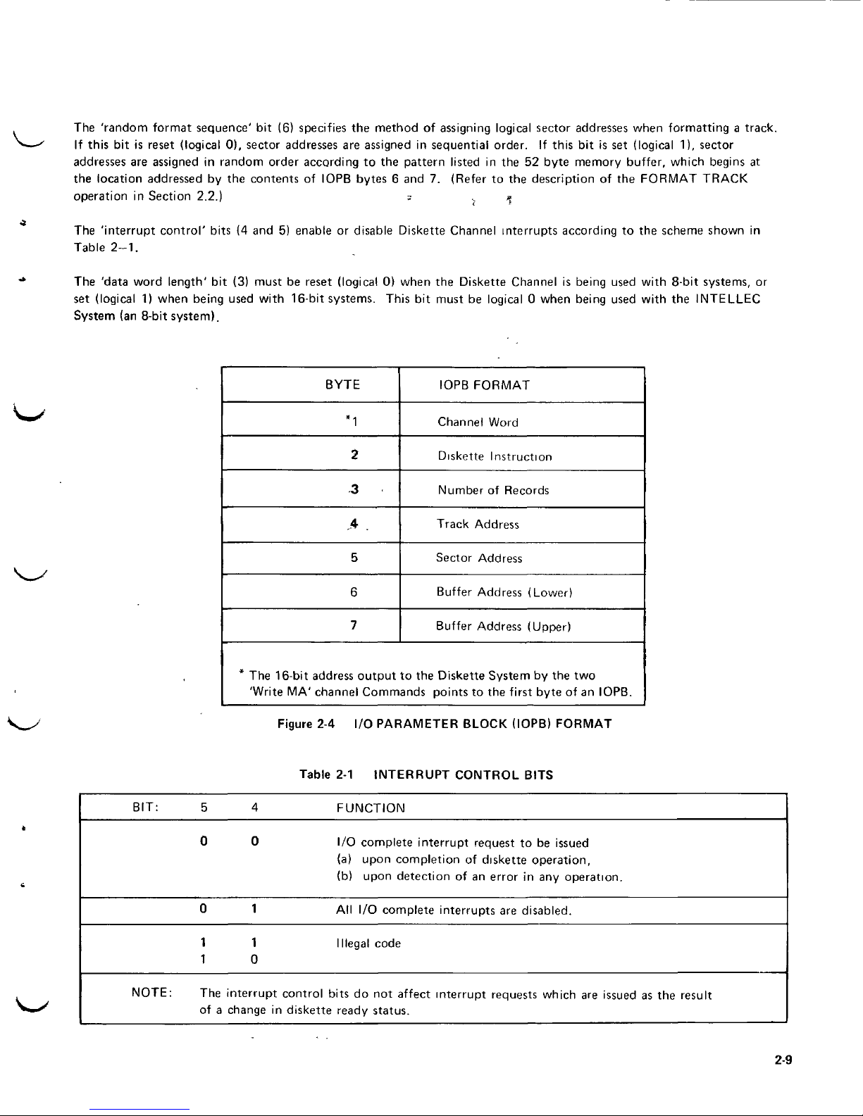
The
'random
format
sequence'
bit (6)
specifies
the
method
of
assigning
logical sector
addresses
when formatting a track.
If
this
bit is
reset
(logical
0),
sector
addresses
are
assigned
in
sequential order.
If
this
bit is set
(logical
1),
sector
addresses
are
assigned
in
random order
according
to the
pattern listed
in the 52
byte
memory buffer, which
begins
at
the
location
addressed
by the
contents
of
IOPB bytes
6 and 7.
(Refer
to the
description
of the
FORMAT TRACK
operation
in
Section 2.2.)
«
,
*
The
'interrupt
control'
bits
(4 and 5)
enable
or
disable
Diskette Channel interrupts according
to the
scheme
shown
in
Table
2-1.
The
'data
word
length'
bit (3)
must
be
reset
(logical
0)
when
the
Diskette Channel
is
being
used
with
8-bit
systems,
or
set
(logical
1)
when being used
with
16-bit
systems.
This
bit
must
be
logical 0 when being used
with
the
INTELLEC
System
(an
8-bit
system).
BYTE
*1
2
3
.4
5
6
7
IOPB
FORMAT
Channel
Word
Diskette
Instruction
Number
of
Records
Track Address
Sector
Address
Buffer
Address
(Lower)
Buffer
Address
(Upper)
* The
16-bit
address
output
to the
Diskette System
by the two
'Write
MA'
channel Commands points
to the
first byte
of an
IOPB.
Figure
2-4 I/O
PARAMETER BLOCK
(IOPB)
FORMAT
Table
2-1
INTERRUPT CONTROL BITS
BIT:
NOTE:
5
4
0 0
0 1
1 1
1
0
The
interrupt
of a
change
in
FUNCTION
I/O
complete interrupt request
to be
issued
(a)
upon
completion
of
diskette operation,
(b)
upon detection
of an
error
in any
operation.
All I/O
complete interrupts
are
Illegal
code
disabled.
control bits
do not
affect interrupt
requests
which
are
issued
as the
result
diskette
ready status.
2-9
Page 30
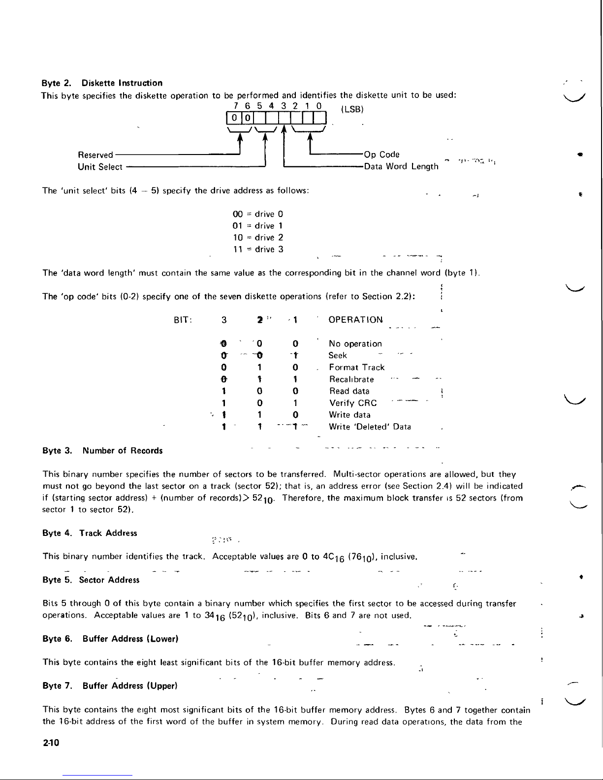
Byte
2.
Diskette Instruction
This
byte
specifies
the
diskette operation
to be
performed
and
identifies
the
diskette
unit
to be
used:
76543210
0
|0
(LSB)
Reserved
—
Unit
Select
•Op
Code
-Data
Word Length
-;•-
-A-
The
'unit
select'
bits
(4 — 5)
specify
the
drive
address
as
follows:
00 =
drive
0
01 =
drive
1
10 = drive
2
11 = drive
3
The
'data
word
length'
must contain
the
same
value
as the
corresponding
bit in the
channel
word
(byte
1).
The
'op
code'
bits (0-2) specify
one of the
seven
diskette operations
(refer
to
Section 2.2):
BIT:
3
2: 1
OPERATION
®
&
Q
0
1
1
t
1
0
^
1
1
0
0
1
t
0
r
0
i
0
1
0
—
t
No
operation
Seek
"
""
'
Format Track
Recalibrate
Read
data
Verify
CRC ' "~
™~
Write data
Write
'Deleted'
Data
Byte
3.
Number
of
Records
This
binary number
specifies
the
number
of
sectors
to be
transferred.
Multi-sector
operations
are
allowed,
but
they
must
not go
beyond
the
last
sector
on a
track (sector 52);
that
is, an
address
error (see Section 2.4) will
be
indicated
if
(starting sector
address) + (number
of
records)>
52-jQ.
Therefore,
the
maximum block transfer
is
52
sectors
(from
sector
1 to
sector 52).
Byte
4.
Track
Address
This
binary
number identifies
the
track. Acceptable
values
are 0 to
4C-|g
(76-|Q),
inclusive.
Byte
5.
Sector
Address
Bits 5 through
0 of
this
byte
contain a binary
number
which
specifies
the
first
sector
to be
accessed
during
transfer
operations.
Acceptable
values
are 1 to
34-jg
(52-)Q),
inclusive. Bits
6 and 7 are not
used.
Byte
6.
Buffer
Address
(Lower)
This
byte
contains
the
eight
least
significant bits
of the
16-bit buffer memory
address.
Byte
7.
Buffer
Address
(Upper)
This
byte
contains
the
eight most significant bits
of the
16-bit buffer memory
address.
Bytes
6 and 7
together contain
the
16-bit
address
of the
first
word
of the
buffer
in
system
memory. During
read
data operations,
the
data
from
the
2-10
Page 31

diskette
is
transferred
to the
buffer.
During
write
operations, data
from
the
buffer
is
written
to
diskette.
During
for-
mat
track operations,
the
address
assignment pattern and/or
the
data field
'format
characters'
are
stored
in the
buffer.
2.4
ERROR
INDICATIONS
If the CPU
executes a 'read
result
byte'
channel command
(in
response
to a
'read
result
type'
channel command
which
returned a code
of
00),
the
Diskette Channel
will
return
the
following
result
word
on the
system data bus:
(LSB)
76543210
Deleted record
CRC
error
Seek
error
Address
error
Data
overrun/underrun error
~*
£-
Not
ready
Write
error
Write protect
1
'
A
The
bits
are
defined
as
follows:
NOT
READY. This
bit (7)
indicates
that
the
selected
unit
was not
ready
or
that
the
selected
unit
changed
to a not
ready
state
during
an
operation.
WRITE
ERROR. This
bit (6)
indicates
that,
during a write operation, a condition
existed which precluded data inte-
grity.
This error
is
detected
by the
drive
and
monitored
by the
Diskette Channel controller.
An
example
of a
condition
that
could
cause
this error
is an
attempt
to
write
through
an
unloaded head.
I
WRITE
PROTECT. This
bit (5)
indicates
that
the
selected drive contains a diskette platter
which
is in the
'read
only'
mode. This
condition
is
checked
on
format track,
write
data
(with
data
address
marks)
and
write
data
(with
deleted
data
address
marks)
operations.
DATA
OVERRUN/UNDERRUN
ERROR.
This
bit (4)
indicates that
the
Diskette System controller
was not
able
to
service a byte
transfer
request
from
the
drive before
the
next request occurred.
The
data byte
is
'lost'.
ADDRESS ERROR. This
bit (3)
indicates
that
the
disk
address
received
from
the CPU is
invalid;
that
is:
•
track
address
>76iQ,
•
sector
address
= 00,
•
sector
address
>52-|Q,
or
•
sector
address + number
of
records>52-|g
SEEK
ERROR. This
bit (2)
indicates
that,
at the
completion
of a
head
movement
sequence,
the
head
is not
positioned
over
the
expected track. This
bit
indicates
the
Diskette System controller and/or drive
are
malfunctioning,
and a
recali-
brate
diskette operation (see Section 2.2)
shoUld
be
performed.
Because
all of the
diskette operations
may
implicitly
cause
the
head
to
move, a seek
error
can
occur
during
any
diskette operation.
I
CRC
ERROR. This
bit (1)
indicates
that
the two CRC
characters generated
during a read data
or
verify
CRC
operation
were
not the
same
as the two CRC
characters
appended
to the
data field (see Section
1.2)
when
it was
written
on
diskette.
DELETED RECORD. This
bit (0)
indicates
that a sector
addressed
during a read
data
or
verify
CRC
operation
was
pre-
ceded
by a
deleted data
address
mark.
I
.
Three
other error conditions
are
indicated when more than
one
error
bit is
true:
I
ID CRC
ERROR.
If the
address
error
(3) and CRC
error
(1)
bits
are
true,
it
indicates
that
the CRC
characters generated
2-11
Page 32

during
the
reading
of an ID
field (see Section 1.2) were
not the
same
as the CRC
characters appended
to the
field when
it
was
written
by a
format
track
operation.
NO
ADDRESS MARK.
If the
address
error (3),
seek
error
(2) and CRC
error
(1)
bits
are
true,
it
indicates
that
no
address
mark (see Section
1.2)
was
encountered
for a
full
revolution
of the
diskette. This usually indicates
that
the
track
has not
been
formatted.
,r.
;
:
,--
-\
DATA
MARK ERROR.
If the
address
error (3),
seek
error (2),
CRC
error
(1),
and
deleted record
(0)
bits
are
true,
it
indicates
that
the
data field
of a
particular sector
was not
preceded
by
either a data mark
or a
deleted data mark.
2-12
Page 33

CHAPTER
3
CHANNEL
BOARD
The
Channel Board
is the
primary control module
within
the
Diskette System.
The
Channel
Board
receives,
decodes
and
responds
to
channel commands
from a Central Processor
Unit
(CPU)
in the
INTELLEC
System.
The
Channel
Board
can
access
INTELLEC System memory
to
determine
the
particular diskette operations
to be
performed
and
to
fetch
the
parameters
required
for the
successful
completion
of the
specified operations.
The
Channel Board
also
monitors
subsystem status
and
error
conditions,
and
organizes
these indications
into
'result
type'
and
'result
byte'
words
that
can be
read
by a CPU in the
INTELLEC System.
The
control
functions
of the
Channel
and
Interface Boards
are
provided
by an
8-bit microprogrammed
processor,
implemented
with
Intel's
Series
3000
Bipolar Microcomputer Set.
The
8-bit controller
includes
four 3002
Central
Processing
Elements (2-bit
slice
per
CPE), a 3001 Microprogram Control
Unit
and 512 x 32
bits
of
3604 pro-
grammable-read-only-memory
(PROM)
which
stores
the
microprogram.
The
processing
and
control
capabilities
of the
diskette controller
are
achieved
by
execution
of the
microprogram.
The
Channel Board
resides
within
the
INTELLEC System cabinet.
The
Channel Board, together
with
the
Interface
Board, constitute
the
Diskette Channel.
3.1
FUNCTIONAL ORGANIZATION
OF
THE
CHANNEL
BOARD
;
,
£
It
For
description purposes,
the
circuitry
on the
Channel Board
can be
divided
into
six
functional blocks (see Figure
3-1):
'. ' ...-_;.-._
•
Channel command block
•;' -
r
\
t
c
•
Micro
control
unit
(MCU) block
--*-—
^
•
Microprogram memory block
•
Central
processing
element (CPE) block
,
•
Data/clock shift
register
(SR) block
!
1
- •
Data
flow
control block
The
CHANNEL COMMAND BLOCK
is
responsible
for
recognizing
and
decoding
channel
commands being
executed
by a CPU in the
INTELLEC
System. When
the
channel command block
recognizes
the
switch-selectable
BASE
address
of the
Diskette System
on the
INTELLEC
System
address
bus,
it
decodes
the
three
least
significant
address
bits
(ADRO/ — ADR2)
to
determine which
of the six
channel
commands
is
being
executed
(see
Section
2.11.
The
three
address
bits
are
also
latched
and
made
available
to the MCU
block,
which
is
ultimately
responsible
for
controlling
the
diskette controller's
response
to a
channel command.
The
channel command block
also
includes
the
interrupt
latch which
stores
the
fact
that
an
interrupt
request
has
been
issued
to the CPU by the
microprogram.
The
MICRO CONTROL
UNIT
(MCU) BLOCK
accepts
and
decodes
the
three
address
bits from
the
channel command
block
(ADRO/ — ADR2/)
specifying a channel
command
or the
three
least
significant
data outputs from
the CPE
block
(DO — D2)
specifying
one of the
seven
diskette operations.
The two
groups
of 3
bits
select
one of the ten
routines which implement
the
channel commands
and I/O
operations.
Having
determined
the
microprogram routine
to be
executed,
the MCU
block then
generates
and
outputs
the
appropriate nine-bit memory
address
from
the
micro-
program
memory.
The MCU
continuously
examines
the two
flag
control
lines
and the
seven
address
control
lines
(AGO — AC6)
from
the
microprogram memory block
to
determine
the
address
of the
next microinstruction
to be
fetched
and
executed.
3-1
Page 34

If)
CO
111
(CO
u
UJ
_J
UJ
I-
Z
;
ADDRESS
LINES
(ADR8/ - ADRF/)
DATA
LINES
DAT
•
<\DD
t
ADR
D/-DATF/)
>
RESS
LINES
O/-
ADR7/
-
DATA
FLOW
CONTROL
BLOCK
MEMORY
DATA
(MDO/-
MD7/)
CPE
DATA
(DO-D7)
fs.
>
(
PF
EL
1
0
:ENTRAL
^OCESSING
EMENT
(CPE)
BLOCK
-*
C
INPU"
SI
STATUS/ERROR
BITS
CHANNEL
COMMAND
BLOCK
ADRO/ - ADR2/
A
4
INPUT
4
DATA/
CLOCK
SHIFT
REGISTER
BLOCK
•^
C
DATA
IN
3
C
CLOCK
1
•t
CLOCK
OUT
V
MICRO
CONTROL
UNIT
(MCU)
BLOCK
A
MASK BITS
FUNCTION
(FO - F6)
ADDRESS
MAO-8
MICRO
PROGRAM
MEMORY
BLOCK
FLAG CONTROL BITS
ADDRESS
CONTROL BITS
DECODER
CONTROL
INTERRUPT
REQUEST
Q
DC
<
O
CO
HI
U.
UJ
z
Figure
3-1
CHANNEL
BOARD:
FUNCTIONAL
BLOCK
DIAGRAM
3-2
Page 35

TABLE
3-3
(CONTINUED)
- -
CONTROL FUNCTION DEFINITIONS (CONTINUED)
- -
RDYRS
—
This
pulse
resets
the
Drive
Ready
flip-flops
on the
Interface
Board.
("-•'•"
..',•
',
;
• •
•«
•'
-'••,>.-
WFLRS
—
This
level
generates
the
write fault
reset
pulse
to the
selected
drive.
GTR43
—
This
pulse
sets
the low
current mode
for
writes
on
tracks
greater
than
43-|rj-
NGT43
—
This pulse
resets
the low
current mode
for
writes
on
tracks equal
to or
less
than
43-|0-
TABLE
3-4
I-BUS
SELECTION
BY
MASK
FIELD
BITS
MASK BITS
M7
=
M6
=
M5
=
M4 =
M3
=
INPUT
FIELDS*
DATA SHIFT
REGISTER
(A36
and
A29)
OUTPUTS
1
0
o
1
0
CLOCK
SHIFT
REGISTER
(A34
and
A27)
<"••
OUTPUTS
1
0
- - o
••••—'
1
1
ERROR
LINES
(DOR,
WRT
PROT,
WRT
ERR,
SEL
DR
NRDY)
1
1
0
0
0
STATUS
LINES
(DRO,
DR1, STOP,
TRACKOO)
1
1
1
0
0
* An
input
field
will
be
multiplexed
into
the I
inputs
of
3002
CPE
array
if the
mask
bits reflect
the
values
listed
for
that field
and if the
K-Bus
select
line,
SO
(bit
9 of the
current microinstruction)
is
high
(logical
1).
Refer
to
Sec-
tion
3.2.4
for a
more complete description
of the
3002
CPE
array
inputs.
3)
Providing generalized inputs
to the
K-bus
inputs
of the
3002
CPE
array.
The
mask
bits
are
multiplexed through
two
8234 multiplexer
devices
and
into
K-bus
inputs
of the CPE
;
:
array.
The
selection
bits
are
provided
by SO and S1
(bits
9—10
of the
current micro-
instruction). Table
3—5
correlates
the
levels
on the SO and S1
lines
with
the
K-bus
inputs.
3.2.4 Central
Processing
Element (CPE) Block
;
The
central
processing
element
(CPE) block
executes
the
function indicated
by
each
microinstruction
output
from
the
microprogram memory.
The CPE
block
includes
an
array
of
four Intel 3002 Central
Processing
Elements,
as
well
as
four 8234
and one
8233 eight-to-four multiplexers that provide
various
inputs
to the CPE
array,
as
shown
on
sheet
4 of the
board schematic (Section 3.3).
3-12
Page 36

If a
'stop
diskette
operation'
command
is
being
received,
output 3 from
the
decoder
goes
true,
asserting
a low
level
\
_/
on the SET
STOP/
line (pin
P2-31).
The
subsequent low-to-high transition
on SET
STOP/
clocks
the
stop latch
reset
(i.e.,
the
active-low state). After
the
stop latch
is
sampled,
the
microprogram
presets
(i.e.,
clears
to the
non-
active-high
state)
the
latch.
If a
'reset
channel'
command
is
being received,
output 7 from
the
decoder
goes
true,
asserting
a low
level
on the
RESET/
line
to the
Interface Board (pin P2-49).
3.2.2 Micro Control Unit (MCU) Block
The
micro
control
unit
(MCU) block provides
the
addresses
for the
microprogram memory. Since
the
micro-
instructions
which
are
fetched from microprogram memory
and
executed
by the
central
processing
elements
define
the
specific functions performed
by the
Channel Board,
the MCU
block
can be
considered
the
primary
source
of
control
for the
diskette controller.
In
addition
to an
Intel
3001 Microprogram
Control
Unit
device,
the MCU
block
includes
an
8234 eight-to-four multiplexer, a 74151 eight-to-one multiplexer
and a few
gating circuits,
as
shown
on
sheet
3 of the
board schematic (Section 3.3).
'
-
—-
'
--^.
V^X
The
Intel
3001 Microprogram
Control
Unit
controls
the
sequence
in
which
microinstructions
are
fetched
from
the
microprogram
memory.
Its
functions
include
the
following:
•
,
-.
-
(A
functional
block
diagram
of the
3001
MCU is
shown
in
Figure
3—2.)
• ' ,
•
Maintenance
of the
microprogram address register
•
Selection
of the
next microinstruction
based
on the
contents
of the
microprogram
address
register
•
Decoding
and
testing
of
data supplied
via
several
input
busses
to
determine
the
microinstruction execution
sequence
*
. •
Saving
and
testing
of
carry
output
data
from
the
central pro-
;
cessor
(CPE) array
,.. j
_.
^_.
-} •
Control
of
carry/shift
input
data
to the CPE
array
•
Control
of
microprogram interrupts
r
Address
control
information
is
supplied
to the
3001
at
inputs
AGO — AC6.
AC1 — AC6 are
provided directly
from
bits
27 — 32 of the
microinstruction
currently
being fetched
from
microprogram memory (see Section
3.2.3).
The
AGO
input,
however,
is
supplied
by the
output
of the
74151 eight-to-one multiplexer.
Five
control
lines from
the
Interface Board (AZ,
INDEX,
XFER REQ,
TIME
OUT and F), one
line
from
the CPE
block (CO)
and one
line
from
the
channel command block (BUSY START)
are
applied
to the
74151
inputs
along
with
the
AGO
bit
(bit
26)
from
the
microinstruction currently being fetched.
The
three
select
lines applied
to the
A, B and C
inputs
on the
74151
section specify which
of the
eight
lines
are
actually multiplexed
through
to the
AGO
input
on the 3001
device.
The three
select
lines
are supplied by bits 14, 15 and 16
(INO,
IN1 and IN2) of
the
current microinstruction. Table
3—1
correlates
the
values
in bit
positions
14, 15 and
16
of the
current micro-
instruction
with
the
control
line
which
is
multiplexed
into
the
AGO
input
on the
3001 section.
The
'flag
logic'
input
(F1)
to the
3001
device
(pin
17) is
also
provided
by CO. The
level
on the CO
line
will
re-
flect
the
'Carry
out'
output
from
the
3002
Central
Processing
Element (CPE)
at A21 or the
'shift
right'
output
from
the
3002
CPE at
A23.
The
'clock'
input
(CLK)
to the
3001
device
(pin
19) is
supplied
by
CLK1/
(pin P2-3) which
is one of the two
clock
pulses
generated
on the
Interface Board (see Chapter
4).
The
load
input
(LD)
to the
3001 (pin
36) is fed by the
master
reset
(MR)
signal
from
the
Interface Board (pin
P2-56).
3-5
Page 37

Recall
from
Chapter
2,
that
the CPU
specifies channel operations
for the
Diskette System
by
executing
one of the
seven
channel commands. A channel
command
may be the
result
of
either
an
input
or
output
instruction
to a
\
/
dedicated
I/O
port
address
on the
Channel Board:
1)
Write
MA
Lower
(output
to
'BASE+1')
2)
Write
MA
Upper
and
start
I/O
(output
to
'BASE+2')
3)
Stop
Diskette
Operation
(output
to'BASE+3')
•-
^
4)
Reset
Channel
(output
to
'BASE+7')
5)
Read
Subsystem Status
(input
to
'BASE+0')
6)
Read Result
Type
(input
to'BASE+1')
......
- *
7)
Read Result
Byte
(input
to
'BASE+3')
The
three
least
significant bits (ADRO/ - ADR2/)
of the
8-bit
I/O
address
(received
at
pins P1-51
through
P1-58)
differentiate between
the
various
input
or
output
channel commands.
The
five most significant
address
bits
(ADR3/
ADR7/)
select
the
Channel Board
if
they match
the
BASE
address
that
is
assigned
by
setting five positions
of
switch
S1.
These five switch positions each feed
one
input
on
five
EXCLUSIVE-OR
gates.
If
ADR3/ - ADR7/
match
the
switch-selected
BASE address,
the
7410
NAND
gate (A31
-8) is
activated
and,
in
turn,
enables
one of the two
3205
decoders.
\~^s
If an
input
channel
command
is
being received,
the RD CMD
line (pin P2-60)
will
be
true,
and the
3205
decoder
at
A20
will
be
enabled. Address bits ADRO — ADR2 (once inverted)
are
applied
to the
three data
inputs
on the
3205
section
(AO —
A2),
and
activate
one of
three inverted
outputs
(Og,
0^
or
03),
depending
on the
channel
command.
If it is
'read
subsystem
status'
command,
output 0 goes
true
and
READ
INT/
is
asserted
at pin
P2-57.
(On the
Inter-
face
Board, READ
INT/
is
used
to
gate
the
device D and
device 1 ready indicators
onto
system data
bus
lines
0 and
1,
DAT0/
and
DAT1/.)
The low
level
on
READ
INT/
also
enables
two
8093
circuits,
one of
which
transmits
the
output
of the
interrupt
latch
(INT/)
to the
data
bit 2
line
(DAT2/)
of the
system data bus.
The
other
8093
circuit
transmits a low-level
to the
data
bit 3
line
(DAT3/),
indicating
that
the
diskette controller
is
present.
INT/
is
also
passed
to the
Interface Board
via pin
P2-40.
^—
If a
'read
result
type'
command
is
being received,
output 1 from
the
decoder
goes
true,
and the RD
Rl/
signal
is
generated
(pin P2-37).
The low
level
on RD
Rl/
pre-sets
the
interrupt
latch (A37-1
0),
thus removing
the
active-low
system
interrupt
request
(INT/).
The
interrupt
latch
can
subsequently
be
clocked
reset
(i.e.,
reset
to the
active-low
state)
by a
pulse
on the CLK
line,
when
the
central processing element
block
(Section
3.2.4)
determines
that
an
'I/O
complete'
or
'ready
status
change'
"^
interrupt
should
be
issued
(also
refer
to
Chapter
2).
If a
'read
result
byte'
command
is
being received,
output 3 from
the
decoder
will
go
true,
and the 741 75
quad
latches
are
clocked, latching
up
address
bits ADRO — ADR2.
The
three most significant quad latch
outputs
are
made
available
to the
micro
control
unit
block
(Section 3.2.2),
which
responds
to
this command
via a
routine
stored
in
microprogram
memory.
Either
read result
command
will
generate
the RD
RES/
signal
which
is
used
by
the
data
flow
control
block (Section 3.2.6)
to
gate
the
appropriate status
word
onto
the
system data bus.
»
If an
output
channel
command
is
being received,
the WRT CMD
line (pin P2-53)
will
be
true,
and the
other
3205
decoder
will
be
enabled. Address bits ADRO - ADR2
are
applied
to
inputs
AO - A2,
causing
one of the
eight
inverted decoder
outputs
to go
true.
If
outputs
0, 1 or 2 go
true,
the
WSUB1/
line (pin P2-48)
is
activated.
If
outputs
*
4, 5 or 6
from
the
decoder
go
true,
the
WSUB2/
line
(pin
P2-47)
is
activated. Either
WSUB1/
or
WSUB2/
will
cause
the
74175 quad latches
to be
clocked
and
latch
up
address
bits ADRO — ADR2, just
as a
'read
result
byte'
command
did.
The
three most significant
outputs
of the
quad
latches
are
made
available
to the
micro
control
unit
block
which
responds
to the
'write
MA
lower',
the
'write
MA
upper
and
start
I/O'
and the
'read
result
byte'
channel
commands,
using routines stored
in
microprogram
memory.
The
response mechanisms
for the
other channel commands
are
implemented
in
hardware,
not
microcode.
'
""•
3-4
Page 38

The
four
'flag
logic
control'
inputs (FCO — FC3)
to the
3001
device
are
provided
by
bits
17 and
18
of the
current
microinstruction.
Bit 17 is
applied
to
both
FCO
(pin
15) and FC1
(pin
16)
while
bit 18
is
applied
to FC2
(pin
13)
and
FC3
(pin 12).
The
'enable'
(EN)
and
'enable
row
address'
(ERA) inputs
to the
3001
(pins
25 and 35,
respectively)
are
held high.
Unless
the
active-low
master
reset
(MR/)
signal
from
the
Interface Board
is
true
(low),
the
'secondary
instruction
bus'
inputs (SXO — SX3)
to the
3001
device
(pins
10, 8, 6 and 5,
respectively)
will
reflect
the
complement
of the
level
on the
four
least
significant memory
address
outputs (MAO - MAS).
That
is, SXO =
MAO,
SX1 =
MA1,
SX2
= MA2 and SX3 - MAS
if
MR/
is
false
(high).
If
MR/
is
true (low),
the
four
SXn
inputs
will
all be
high,
regardless
of the
state
of the MAn
outputs.
The"
four
'primary
instruction
bus'
inputs (PX4 — PX7)
to the
3001
device
are fed by the
four inverting outputs
of
the
8234 eight-to-four multiplexer (A5).
The
multiplexer outputs
are
controlled
by the
levels
on the SO and S1
inputs.
.
-
»
-
i' i - - -\
The
A1,
A2 and A3
inputs
to the
8234 section
are the
three
least
significant data outputs from
the
central pro-
cessing
element (CPE) block that
have
been
buffered
and
inverted;
the AO
input
is
always
high. After
having
fetched
the
diskette instruction byte from
the I/O
Parameter
Block
in
system
memory (see Section 2.3),
the CPE
block
will
output
the
three bits
that
specify
one of the
seven
diskette operations
onto
its
three
least
significant
data
outputs
(DO - D2).
Table
3-1
AGO
INPUT SELECTION
Select
Lines
ACO
Input
At
3001
MCU
(Bit
14)
(Bit
15)
(Bit
16)
(Pin
39)
0
0
0
0
0
1
0
Bit 26 of
current microinstruction (ACO)
CO:
The
carry
out
output
from
the
3002
CPE at A21
or
the
shift right
output
from
the
3002
CPE at
A23.
BUSY
START:
Indicates
that a 'write
MA
lower',
'write
MA
upper'
or
'read
result
byte'
channel
command
has
been
received.
F
(pin
P2-58):
Indicates
that
data/clock shift
registers
are
full
during
read
or
empty during write.
AZ
(pin
P2-41):
Indicates a valid
CRC
check
(all
zeros).
INDEX (pin P2-42):
Indicates
that
an
index mark
has
been
detected (i.e.,
the
beginning
of a
track).
XFER
REQ
(pin
P2-39):
Indicates
that
Interface
Board
has
requested
use of the
INTELLEQ
MDS
system
bus.
TIMEOUT
(pin P2-38):
Ten
millisecond
pulse
that
is
used
by the
microprogram
for
general
timeouts.
3-7
Page 39

ENABLE
ROW
ADDRESS
ERA
MAs
MICROPROGRAM MEMORY
ADDRESS
MA4
---- MAQ
INTERRUPT
STROBE
ISE
ENABLE
AC
6
AC5
ADDRESS
AC
4
CONTROL
ACa
FUNCTION
AC2
Ad
AC
0
LOAD
LD
r
h—J±ti±—±LLt
LM
^
nilTPIIT
1 I
OUTPUT
r
OUTPUT
BUFFER
OUTPUT
BUFFER
MICROPROGRAM
ADDRESS
REGISTER
•EN
MCU
OUTPUT
ENABLE
NEXT
ADDRESS LOGIC
pp2 PROGRAM
-|—
PRi
LATCH
PRO
OUTPUTS
L
_i
J,
7
FCQ
FLAG
FLAG
LOGIC
INPUT
CONTROL
T
FQ
FC2
FCs
PXj
---- PX4
FLAG
FLAG
PRIMARY
OUTPUT
LOGIC
INSTRUCTION
CONTROL
BUS
~?
Y?~?~
SX3 SXQ
SECONDARY
INSTRUCTION
BUS
Figure
3-2
3001
MICROPROGRAM CONTROL
UNIT:
FUNCTIONAL
BLOCK DIAGRAM
Page 40

2)
Driving
fields (data
8234
puts
field
the
input
shift
and
8233
of the CPE
bits,
as
listed
multiplexers
register,
multiplexer
array.
The
in
Table
TABLE
3-2
to the
3002
Central
clock
shift
register, errors
devices
(see
selection
bits
sheet
for the
4 of the
3—4.
MICROINSTRUCTION
Processing
and
status)
schematic)
multiplexers
BIT
ASSIGNMENTS
Element (CPE) array. Four
are
multiplexed
and
are
provided
into
through
the
I-bus
by the
in-
mask
MICROINSTRUCTION
BIT
01
02
03
04
05
06
07
08
09
10
11
12 - 13
14
15
16
*17
*17
*18
*18
19
20
21
22
23
24
25
26
27
28
"
29
30
31
32
SIGNAL
MASKO
(MO)
MASK1 (M1)
MASK2
(M2)
MASK3 (M3)
MASK4 (M4)
MASK5 (M5)
MASK6 (M6)
MASK7
SLKO
(M7)
(SO)
SLK1 (S1)
OUTO
OUT1
"
"-"-
OUT2
INO
IN1
IN2
FCO
FC1
FC2
FC3
FO
F1
F2
F3
F4
F5
F6
AGO
AC1
AC2
AC3
AC4
•
AC5
AC6
'
~-
-
"~
„
''
•
]
DEFINITION
"*
Mask
field
*
*
K-bus
select
.
Decoder
select
AGO
Select
Flag
•*
control
Function field
Address
output
control
PROM
LOCATION - PIN
A13-
A13-10
A13-11
A13-13
A13-14
A13-15
A13-16
A13-17
A12-
A12-10
A12-11
A12-13
A12-14
A12-15
A12-16
A12-17
A11A11-
A11-10
A11-10
A11-11
A11-13
A11-14
A11-15
A11-16
A11-17
A10-
A10-10
A10-11
A10-13
A10-14
A10-15
A10-16
A10-17
9
9
9
9
9
*Bit
17
drives
FCO and
FC1;bit
18
drives
FC2 and FC3
3-9
Page 41

At
this
time,
the
mask
and
output
bits
of the
current microinstruction being
output
from
the
microprogram memory
block
(see
Section 3.2.3)
will
produce a high
level
on the SO
input
to the
8234 section
and a low
level
on the S1
input,
multiplexing
the
inverted
levels
of the
8234's A inputs
(specifying a particular diskette operation)
into
the
PX4 — PX7
inputs
on the
3001 MCU. This
allows
the
3001
MCU to
subsequently
access
those
microinstructions
which
will
effect
the
appropriate diskette operation.
The B1, B2 and B3
inputs
to the
8234 multiplexer
are the
three
least
significant
system
address
bits
that
were
buffered
and
inverted
in the
channel command block (see Section 3.2.1);
the BO
input
is
always
held low.
Recall
that
these
three
address
bits
specify
one of the
seven
channel
commands.
At
this
time,
the
mask
and
output
bits
of the
current
microinstruction being
output
from
the
microprogram memory block (see Section 3.2.3)
will
produce
a low
level
on the
SO
input
to the
8234 section, multiplexing
the
inverted
levels
of the
8234's B inputs
(specifying a particular channel
command)
into
the PX4 - PX7
inputs
on the
3001 MCU. This allows
the
3001
MCU to
subsequently
access
those
microinstructions
which
will
produce
the
proper Diskette System
response
to the
channel
command
received.
The
MCU
outputs
the
9-bit
address
of the
next microinstruction
to be
fetched
on MAO -
MAS.
MAO -
MAS
are
applied
to the
nine
address
inputs
on
each
of the
3604
PROM's
that
constitute
the
microprogram memory (see
Section
3.2.3).
"
'
r
'
"'
3.2.3 Microprogram Memory Block
The
microprogram memory block
stores
the
microinstructions which direct
the
operation
of the
diskette controller.
The
microprogram memory block
consists
of
four 3604
programmable-read-only-memory
devices
(512
x 8
bits
each),
which
store
32 bit
microinstructions; a 3205 three-to-eight decoder, which
generates
eight timing control
pulses
(DEC
OUTO
- DEC
OUT7)
based
on
bits
11,
12
and 13
(OUTO - OUT2)
of the
current microinstruction;
and a
3404
six-bit high
speed
latch,
which
provides
various
control
signal
levels
based
on the
decoder outputs mentioned
above
and the
mask
bit
field
of the
current microinstruction;
as
shown
on
sheet
3 of the
board
schematic
(Section
3-3).
_ .
_
_ I
The
9-bit
memory
address
(MAO - MAS)
for the
four
3604
PROM's
is
provided
by the
3001 Microprogram
Control
Unit.
MAO —
MAS
cause
the
addressed
microinstruction
to
appear
on the 32
output
lines
from
the
four
PROM's.
Table
3-2
summarizes
bit
definitions
for the
32-bit microinstructions.
The
address
control bits,
AGO
— AC6
(bits
26-32),
the
flag
control bits (bits
17 and
18),
and the
input
control bits
used
for
AGO
select
(bits
14-16)
are fed
to the
micro control
unit
block
as
described
in
Section 3.2.2.
The
function field bits,
FO — F6
(bits
19—25),
the
mask
bits
MO - M7
(bits
1—8)
and the
K-bus
select
bits
SO and S1
(bits 9-10)
are
applied
to the
central pro-
cessing
element (CPE) block,
as
described
in
Section 3.2.4.
The
output
bits OUTO - OUT2 (bits
11-13)
are
applied
to the
three
address
inputs
on a
3205
decoder.
The
enable
inputs
to
this 3205 section
are
provided
by the
CLK2/
pulse
from
the
Interface
Board (pin
P2—30),
the
seventh
mask
bit M7
(bit
8 of the
current microinstruction)
and
SO, one of the two
K-bus
select
bits mentioned
above
(bit
9 of the
current
microinstruction).
The
eight decoder
outputs,
DEC
OUTO
— DEC
OUT7,
provide
timing
control
pulses
that,
when
used
with
the
mask
bits,
provide
over-
all
control
for the
diskette controller (see Table
3—3).
The
mask
field bits
MO — M7
(bits
1—8
of the
current microinstruction)
are
actually
used
for
three disjoint functions
in the
Diskette System:
?
[
*
" ' '
;
$
*
j
1)
Generating
control
signals
for the
hardware.
These
control
signals
are
pulses
(positive
or
|
negative
and of
50—75
nsec.
duration)
or
levels.
The
pulses
are
generated
by
gating
the *
appropriate
mask
bit
with
one of the
3205
decoder
outputs (DEC OUTn).
The
levels
are
"
derived
by
using
the DEC
OUTn outputs
to
strobe 3404 six-bit
latches.
The DEC
OUTn
<
outputs provide
the
write
enable
strobes
to the
3404
latches,
while
the
mask
bits provide
the
data
inputs and, consequently,
the
actual
controls.
Refer
to
Table
3—3
for a
summary
I
of the
control
pulses
and
levels
generated
by the DEC
OUTn
strobes
and
mask
field
bits.
5
3-8
Page 42

TABLE
3-3
(CONTINUED)
CONTROL
FUNCTION
DEFINITIONS
(CONTINUED)
SROUT
-
This
level
enables
data bits
from
data
register
(when high)
or
from 9401
CRC
device
(when
low)
to be
sent
to the
selected
diskette.
LDADM
-
This
level
is
used
to
load clock shift
register
with
the bit
patterns required
to
write
the
different
address
marks
onto a diskette.
CRCMD
This
level
indicates
the
operating mode
for the
9401
CRC
device
on the
Interface
Board.
DIREC
—
This
level
indicates
the
direction
of
head
movement
for the
selected
diskette drive.
AMWRT
—
This
level
enables
writing
of an
extra clock
pulse
and is
activated during
writing
of an
address
mark.
-
~
,„
LOWEN
STBDL
LDADD
This
level
drives
the
GATE LOWER line that
enables
data
onto
the
memory data
inputs
(MO/ - M7/)
to the
CPE
array.
MEMWT
—
This level indicates when
the
Diskette System
wishes
to
write
data
to
memory.
SMREQ
—
This
pulse
initiates
the bus
request
sequence
intended
to
gain
master
control
of the
INTELLEC
MDS
system
bus.
.
|
I
STBDU
—
This pulse loads
CPE
data
outputs
(DO — D7)
into
the
latch
which
drives
the
system data
lines,
DATA8/ - DATAF/.
This
pulse
loads
CPE
data outputs
(DO — D7)
into
the
latch which
drives
the
system
data
bus
lines, DATAO/ - DATA?/.
J
This
pulse
loads
CPE
data outputs
(DO — D7)
into
the
latch which
drives
the
system
address
bus
lines,
ADRO/ - ARD7/.
:
.
{
SINTR
This
pulse
is
used
to
generate a signal
which
clocks
the
interrupt latch
on the
Channel
Board.
CINBS
—
This
pulse
is
used
to
latch
data
from
the
system
data
bus
into
the
latches
which drive
M0 - M7/
of the
CPE
array.
CSYNC
—
This pulse initializes
the
synchronization logic prior
to
detecting
an
address
mark.
RSAMD
—
This
pulse
resets
the
synchronization logic
prior
to
initializing
the
logic
with
the
CSYNC
pulse.
UNLHD
-
This
pulse
clears
the
LOAD
latch
on the
Interface Board,
and
ultimately
causes
the
read/
write head
on the
selected
drive
to be
unloaded.
RSTST
This
pulse
is
used
to
generate
CLR
START STOP signal
which
resets
the
STOP
latch
and
the
74145 latch
at
A8-1
on the
Channel Board.
RNDX
-
This pulse
resets
the
INDEX latch
on the
Interface Board.
LDOPC
—
This pulse latches diskette operation code
(DO—D5)
and
makes
latched code
available
to
'primary
instruction
bus'
multiplexer.
3-11
Page 43

TABLE
3-3
CONTROL PULSES
AND
LEVELS GENERATED
BY
MICROPROGRAM
OUT
CODE
(DEC
OUT n)
MASK
BIT
MO
M1
M2
M3
t-^.
M4
M5
M6
000
(0)
CSTEP
SSCLK
LDHD
001
(1)
RDYRS
_.
RINH
SINH
SACK
RDOR
010
(2)
NSUBO
NSUB1
- — --
-
'
011
(3)
LDNXM
WTGTN
SR
OUT
LDADM
100
(4)
_
-_.
-
CRC
MD
DIREC
101
(5)
AMWRT
WFLRS
—
~.-?_
LOWEN
MEMWT
•
i
i
110
(6)
SMREQ
STBDU
STBDL
LDADD
GTR43
SINTR
CINBS
111
(7)
CSYNC
RSAMD
UNLHD
RSTST
NGT43
RNDX
LDOPC
CONTROL
FUNCTION DEFINITIONS
CSTEP
SSCLK
LDHD
RINH
SINH
SACK
This pulse triggers
the
one-shot which
drives
the
STEP/
line
to the
diskette drives.
STEP/
causes
the
selected
drive
to
move
its
head
one
track.
i
This pulse
triggers
the
TIMEOUT one-shot. TIMEOUT
provides
a 10
msec,
pulse
for use by the
microprogram.
...._,.
This
pulse
sets
the
LOAD
latch
on the
Interface Board
which
causes
the
read/write
head
on the
selected
unit
to be
loaded.
t,
'
*
This
pulse
resets
the
inhibit
memory write latch
(A48—1).
L,,.
?
This
pulse
sets
the
inhibit
memory write latch
(A48—4).
"
~
This pulse
sets
the
transfer
acknowledge (XACK/) latch
on the
Interface Board.
RDOR
—
This pulse
resets
the
data overrun latch
on the
Interface Board.
-.
NSUBO
and
NSUB1
-
These
levels
select
'primary
instruction
bus'
inputs
to
3001 MCU.
LDNXM
-
WTGTN
rc
r
-.t
This
level
is
used
to
load
the
clock
shift
register
with
the bit
patterns required
to
write
the
different
address
marks
onto a diskette.
When
the
data
and
clock shift
registers
are
empty,
this
level
allows
both
shift
registers
to
be
parallel
loaded
with
information
that
will
be
serially
shifted
out to the
Interface Board
and
then
to the
diskette. Used
to
generate
PE/ and WRT GT/
signals.
3-10
Page 44

An
Intel 3002 Central
Processing
Element contains
all of the
circuits that
represent a 2-bit wide
slice
through
the
data
processing section
of a
digital
computer. When wired together
in an
array,
a set of
CPE's
provide
the
following
capabilities:
•
Two's complement arithmetic
•
Logical AND,
OR, NOT and
EXCLUSIVE-OR
•
Incrementing
and
decrementing
•
Shifting left
or
right
• Bit
testing
and
zero
detection
•
Carry
look-ahead
generation
•
Multiple
data
and
address
busses
A
functional block diagram
of a
3002
CPE is
shown
in
Figure 3-3.
TABLE
3-5
K-BUS
INPUT
SELECTION
K-BUS
SELECT LINES
S1
(Bit
10)
o
0
1
SO
(Bit
9)
:
Q..
'
1
-1
K-BUS
INPUTS
TO
3002
CPE
ARRAY
KO
MO
1
0
K1
M1
1
0
K2
M2
1
0
K3
M3
1
0
K4
M4
1
0
K5
M5
1
0
KG
M6
1
0
K7
M7
1
0
Note that
only
when
SO and S1
equal zero
will
the
K-bus
inputs
be
supplied
by the
mask
bits; otherwise,
the
K-bus
inputs
will
be all
ones
or all
zeros.
*
During
each
micro-cycle,
the
function
field
of the
current
microinstruction
is
applied
to the
F-bus
inputs
(FO — F6)
of
each
3002 CPE.
The
function bits
are
decoded,
the
operands
are
selected
by the
internal multiplexers,
and the
specified
operation
is
performed. Within
each
CPE,
data
is
stored
in
eleven
scratchpad
registers
or the
accumulator.
Data
being
output
from
the CPE
array
is
carried
on the
address
bus (AO — A7) or the
data
out bus (DO —
D7).
The
address
outputs drive
the
eight most significant
lines
of the
INTELLEC
System
address
bus, ADR8 — ADRF.
The
data
outputs
are
made
available
to the
data flow control block (Section 3.2.6)
and the
micro control
unit
block (Section
3.2.2).
Data
is
brought into
the CPE
array
on
three
separate
input
buses,
the
memory
data
bus (MO -
M7),
the
l-bus
(10 - 17)
and
the
K-bus
(KO —
K7).
The
memory
data
inputs
are
supplied
by the
data flow control block
(Section
3.2.6)
which
routes
data
from
the
system
data
bus to the CPE
array.
The
latter
two
buses
are
driven
by
five
multiplexers.
The
K-bus
inputs
(KO - K7) are
driven
by two
8234 eight-to-four multiplexers
(located
at A33 and
A26).
The SO and
S1
outputs from
the
microprogram memory
(bits
9 and 10 of the
current microinstruction) determine
the
four outputs
on
each
of the two
8234
sections.
If SO = 1
andS1
= 0, all
eight
inverted
outputs will
be
low.
If SO = 1 and S1 = 1,
3-13
Page 45

MAIN
MEMORY
ADDRESS
M
A
0
r
ENABLE
ADDRESS
EA
—6—«•
LOOK AHEAD
CARRY
OUTPUTS
X
CARRY
OUT
CO
—O-
LEFT
IN L1
—O
CLK
H
-i
MICRO-FUNCTION
BUS
GND
F5
F2
FO
OUTPUT
BUFFER
MEMORY
ADDRESS
REGISTER
MICRO
FUNCTION
DECODER
DATA
OUT
—J
DO
*
£
OUTPUT
BUFFER
AC
REGISTER
ARITHMETIC/LOGIC
SECTION
MULTIPLEXER
A
/
i
i
/
i
MULTIPLEXER
B
SCRATCHPAD
REGISTERS
R0-R9,T
o—<
M1 M
0
MEMORY
DATA
IN
o—o
EXT
DEVICE
IN
o—o
K1 K
0
MASK
IN
-p
ED
ENABLE
DATA
Cl
CARRY
IN
-O—
RO
RIGHT
OUT
Figure
3-3
3002
CENTRAL PROCESSING
ELEMENT:
FUNCTIONAL
BLOCK
DIAGRAM
3-14
Page 46

all
eight outputs
will
be
high.
If SO = 0,
however,
the
eight
mask
bits,
MO — M7,
from
the
microprogram memory
(bits
01 — 08 of the
current microinstruction) will
be
inverted
and
applied
to the
K-bus
inputs
of the CPE
array
(see
Table
3-5).
The
l-bus
inputs
(10 — 17)
are
driven
by two
8234
(inverting
outputs)
and one
8233
(non-inverting
outputs)
eight-to-
four multiplexers (located
at
A28,
A45 and
A35).
Mask
bits
M3 - M7
from
the
microprogram memory (bits
04 - 08
of the
current
microinstruction)
determine
the
l-bus inputs
as
listed
in
Table
3—4
of
Section
3.2.3.
These mask
bits
will
enable
the
eight outputs from
the two
4-bit
data
shift
registers
(at A36 and
A29),
or the
eight outputs
from
the
two
clock shift
registers
(at A34 and
A27) through
the
8233
section
and one of the
8234
sections
and
into
the
10 — 17
inputs
on the CPE
array.
The
mask
bits
can
also
enable
the
four error
lines
(DOR,
WRT
PROT,
WRT ERR and SEL DR
NRDY)
or the
four
status
lines
(DRO, DR1, STOP
and
TRACK
00)
from
the
Interface Board (see Chapter
4)
through
the
other 8234 section
(at
A45)
and
into
the
14 — 17
inputs
on the CPE
array.
The
clock
input
to the
3002
CPE's
is
provided
by the
CLK1/
pulse
generated
on the
Interface Board.
The
enable
address
inputs
(EA),which
enable
the
address
outputs
(AO —
A7),
are fed by the
SELECTED line
from
the
Interface
Board
(pin
P2-43).
When true, SELECTED
indicates
that
the
diskette controller
has
master
control
of the
INTELLEC
MDS bus
(see Chapter
4). The
enable
data
input (ED)
to
each
3002
CPE is
permanently held
low
(active).
The
carry
output
(CO) from
each
3002
CPE
feeds
the
carry
input
(CD of the
adjacent
3002 CPE. Likewise,
the
shift
right
output
(RO) feeds
the
shift
right
input
(LI)
of the
adjacent
3002
CPE.
The
carry
output
(CO)
from
the
most
significant
CPE
(A21—7)
feeds
its own
shift right
input
(LI)
and is
wire—ORed
with
the
shift right
output
(RO) from
the
least
significant
CPE
(A23—8)
to
form
the CO
line,
which
is
applied
to the
flag
control
input
(Fl)
on the
3001
Microprogram Control
Unit.
CO is
also
inverted
and
applied
to the D1
input
on the
74151 multiplexer
(A30—3)
which
provides
the
least
significant
address
control
bit,
AGO,
to the
3001 MCU.
The
carry
input
(Cl)
to the
least
significant
3002
CPE
(A23-10)
is
provided
by the
flag control
output
(FO)
from
the
3001 MCU.
3.2.5 Data/Clock Shift
Register
Block
During
read
operations,
the
data/clock shift
register
(SR) block
accepts
serial
data
and
clock bits
that
the
Interface
Board
has
received
from
the
selected
diskette drive
and
converts them
into
eight
bit
bytes
that
are
input,
in
parallel,
to the CPE
array.
During write
operations,
the
shift
registers
are
parallel
loaded
with
data
and
clock bytes which
are
then shifted
out to the
Interface Board. This
block
includes four
9300
four-bit
shift
registers,
as
shown
on
sheet
4 of the
board schematic (see Section 3.3).
Recall
from Section
1.2
that data
and
clock bits
are
interspersed
when information
is
written
on
disk.
When
that
information
is
later read,
the
diskette drive
separates
the
data
and
clock
pulses
before
passing
them
to the
Interface
Board
(see Chapter
4).
The
Interface
Board,
in
turn,
sends
the
data
bits
to the
Channel
Board
via the SR
DATA
IN/
line (pin
P2—22)
along
with
the
data
strobe
SR
DATA
STB
(pin
P2 -
24).
SR
DATA
IN/
feeds
the J and K
inputs
on the
first
data
shift
register
at
A36.
The Q3
output
from
this first shift
register
then
feeds
the J and K
inputs
on the
shift
register
at
A29.
When
the
data
shift
registers
are
full,
the
eight
data
bits
are
transferred
in
parallel
to the CPE
array.
The
four
outputs
from
the
first data shift register (A36)
are
applied
to the
'A'
inputs
on the
8233
multiplexer
that
feeds
the
four
least
significant
l-bus
inputs
to the CPE
array.
The
first
two
outputs
are
also
made
available
to the
Interface
Board
via the I DO/
(pin
P2-26)
and
ID1/
(pin
P2-23)
lines (see Chapter
4). The
four
outputs
from
the
second data
shift
register
(A29)
are
applied
to the
8234 multiplexer (A28) that
feeds
the
four most significant bits
of the
l-bus
inputs
to the CPE
array. Both data shift
registers
are
clocked
by SR
DATA
STB.
During write operations,
both
data shift
registers
can be
parallel loaded when
the PE/
input
is
low.
PE/
will
go low
when
the
shift
register
is
empty
and the
WTGTN
signal
is
true (see Table
3—3).
3-15
Page 47

The
parallel
inputs
to the
first data shift
register
(A36)
are
supplied
by the
four
least
significant data outputs
from
the CPE
array,
as
follows:
DO
^
PO
D1
V
P1
D2
>•
P2
>r
""""
" : '
The
parallel
inputs
to the
second data shift
register
(A29)
are
supplied
by the
four most significant
CPE
array
data
outputs:
,
L/t
nF>
UD
DR
UD
r>7
—
^~ i \j
>.
pi
"
Y \
•to.
P9
^ I <^
^.
PQ
The
data bits
can
then
be_
shifted
out,
in
serial,
to the
Interface Board
via the SR
DATA
OUT
line (pin
P2-25)
which
is
driven
by the Q3
output
on the
second data shift register.
During
read
operations,
the
Interface Board
sends
the
clock bits (that
were
interleaved
with
the
data bits
on the
diskette)
to the
Channel Board
via
the_SR
CLK
IN/
line (pin P2-6) along
with
the
clock strobe,
CLK SR STB
(pin
P2-8).
SR CLK
IN/
feeds
the J and K
inputs
on the
first clock shift
register
at
A34.
The Q3
output
of
this first
clock shift
register
then
feeds
the J and K
inputs
on the
shift
register
at
A27. When
the
clock shift
registers
are
full,
the
eight clock bits
can be
transferred
in
parallel
to the CPE
array.
The
four
outputs
from
the
first clock shift
register
(A34)
are
applied
to the 'B'
inputs
on the
8233 multiplexer
that
feeds
the
four
least
significant bits
of the
l-bus
to the CPE
array.
The
four
outputs
from
the
second
clock shift
register
(A27)
are
applied
to the
8234 multi-
plexer
that
feeds
the
four
most significant bits
of the
l-bus.
Both
clock shift
registers
are
clocked
by CLK SR
STB.
During write operations,
both
clock shift
registers
can be
parallel
loaded when
the PE/
signal
(described
above)
is
low.
The
PO,
P1 and P2
inputs
to the
first clock shift
register
and the P2 and P3
inputs
to the
second
clock shift
regis-
ter
are
tied
to
ground.
The P3
input
to the
first
shift
register
and the P1
input
to the
second
are
both
fed by the
output
of a
7408
AND
gate
(A7-6)
shown
on
sheet
3 of the
schematic.
The
inputs
to
this
gate
are the
LDNXM
and
LDADM
control
levels
which
have
been
set in the
3404
latches
at
A16
by the
microprogram
(refer
to
Table
3—3).
The PO
input
to the
second clock shift
register
is fed by the
LDADM
control
output.
LDNXM
and
LDADM
allow
the
microprogram
to
produce
the
varied
patterns
of
clock
bits
that
are
required
to
write
the
different types
of
address
marks
onto a diskette (refer
to
Section 1.2).
3.2.6 Data Flow
Control
Block
>r
'
''-
-
The
data
flow
control
block routes data
to/from
the
various
other
functional
blocks
within
the
Channel Board. This
block
consis'ts
of
five 8212 bi-directional latching
bus
drivers, a 3404
six-bit latch
and
various
gating circuits,
as
shown
on
sheet
2 of the
board schematic (Section 3.3).
.
-t
The six
least
significant data outputs
(DO — D5)
from
the CPE
array
are
applied
to the
inputs
of the
3404
six-bit
latch. When
the_
microprogram
generates
the
LDOPC control
pulse
(see Table 3-3),
DO - D5 are
latched
and in-
verted.
DO - D2 are
made
available
to the
'primary
instruction
bus'
multiplexer (A5)
in the MCU
block.
D3 is
used
for
16-bit
data
flow
control
as
described
below.
D4 and D5 are
sent
to the
Interface
Board
as the
unit
select
signals,
USA
(pin P2-9)
and USB
(pin
P2-12),
respectively.
All
eight
CPE
data
outputs,
DO - D7, are
also
applied
to
three
of the
8212 latching
bus
drivers.
DO - D7 are
loaded
into
the
8212
device
at A41
when
the
microprogram
generates
the
LDADD
control
pulse
(see Table
3—3).
The
8212
3-16
Page 48

device
at A41
drives
the
eight
least
significant
lines
of the
system
address
bus, ADRO/ - ADR7/,
When
the
micro-
program
generates
the
STBDL
control
pulse (see Table
3-3),
DO - D7 are
latched
into
the
8212
device
at A43
which
drives
the
eight
least
significant
lines
of the
system data bus, DATO/ - DAT7/
(pins
P1 - 67
through
P1 -
74).
STBDL
is
generated when
the
microprogram
is
setting a result word
or
preparing write data. When
the
microprogram
generates
the
STBDU
control
pulse
(see Table 3-3),
DO - D7 are
latched
into
the
8212
device
at
42,
which
drives
the
eight most significant system data
bus
lines,
DATS/ - DATF/
pins
P1 - 59
through
P1 -
66). STBDU
would
only
be
generated
if the
Diskette System were operating
in the
16
bit
mode.
The
address
latch
(A41)
is
gated
onto
the MDS
system
bus
whenever
the
SELECTED
signal
is
true.
The
high-order data latch (A42)
is
gated
onto
the bus
whenever
the
SELECTED,
MEMORY WRITE
and
16-BIT
MODE
signals
are
true.
The
low-order data latch (A43)
is
gated
onto
the bus
during
memory
write
operations
or
'read
result'
operations.
When a master
bus
module
in the
INTELLEC
System
outputs
data
to the
diskette
controller,
the
data
from
lines
DATO/ - DAT7/
is
applied
to the
8212
bus
driver
at
A25.
DATS/ - DATF/
is
applied
to the
8212
at
A24.
The
data
on
those
lines
are
strobed
into
the
input
latches
at A24 and A25 by the
microprogram control
pulse
CINBS
(see
Table
3-3).
'Slave'
memory modules
also
drive
the
data lines,
DATD/ - DAT7/
and
possibly
DAT8/ - DATF/.
Memory data
are
strobed
into
the
latches when
the STB MEM IN
signal
is
generated
by the
Interface Board.
The
outputs from
the
devices
at A24 and A25 are
'OR-ed'
into
lines
MO/-
M7/.
Depending
on the
state
of the
GATE LOWER
signal,
data
from
only
one of the two
latches
will
actually
be
gated
onto
the M
input
lines
(MO/ — M7/)
to the CPE
array.
3.3
SCHEMATICS/PIN LISTS:
CHANNEL
BOARD
The
schematic drawing
(4
sheets)
for the
Channel Board
is
provided
in
Figure 3-4.
These
schematics
are
subject
to
change
without
notice.
The
Reference Schematic Drawings shipped
with
the
Diskette System should
be
used
as a
reference.
Table
3-6
lists
the
pins
and
designated
signal
functions
for the
86-pin
P1 bus
connector. Table
3-7
lists
the
same
infor-
mation
for the
60-pin
P2
controller connector.
TABLE
3-6 PIN
LIST:
P1 BUS
CONNECTOR
PIN
SIGNAL
FUNCTION
1
2
3
4
5
6
7
8
9
10
11
12
13
14
15
16
17
18
NO
CONNECTION
3-17
Page 49

TABLE
3-6 PIN
LIST:
P1 BUS
CONNECTOR (CONTINUED)
PIN
19
20
21
22
23
24
25
26
27
28
29
30
31
32
33
34
35
36
37
38
39
40
41
42
43
44
45
46
47
48
49
50
51
52
53
54
55
56
57
58
59
60
61
62
63
64
65
66
67
68
69
70
SIGNAL
i
--
-•
"-
-
•
-
i
f
"•
>
'
-'
'
*
NO
CONNECTION
"
r
1
•*
.
•
-i
,
-
<
j-
•
r
ADRE/
ADRF/
ADRC/
ADRD/
ADRA/
ADRB/
ADR8/
.
ADR9/
ADR6/
ADR7/
ADR4/
ADR5/
ADR2/
ADR3/
ADRO/
ADR1/
DATAE/
DATAF/
DATAC/
DATAD/
DATAA/
DATAB/
DATA8/
DATA9/
DATA6/
DATA7/
DATA4/
DATA5/
FUNCTION
-
- • •
,."-'
- , •• • '
•• * *
i
:
"
.
»J
»
*•
INTELLEC
System
"~~
~~
~~
,
address
bus
\
'"
~"?""
"
~"
:
r
,
I
*••
-t
~
'
^
I
^
2.
—
'
1
*"*.
'
•t
INTELLEC
System
data
bus
-
3-18
Page 50

TABLE
3-6 PIN
LIST:
P1 BUS
CONNECTOR
(CONTINUED)
PIN
71
72
73
74
75
76
77
78
79
80
81
82
83
84
85
86
SIGNAL
DATA2/
-
"
DATA3/
.-.'
•*•*-,
DATAO/ - .".'-•
.
DATA1/
j
L
* \ f
1~-
NO
CONNECTION
1
i-
r
'
\
"*
*~a~
*
'•
'
H
*•
-^
V
-
,
-
i
1
r
FUNCTION
i
INTELLEC
System
i
data
bus
-
»
£
-•
t
*
TABLE
3-7 PIN
LIST:
P2
CONTROLLER CONNECTOR
PIN
SIGNAL
FUNCTION
1
2
3
4
5
6
7
8
9
10
11
12
13
14
15
16
17
18
19
20
MK4
CLK1/
MK1
SR
CLK IN 1
CLKSRSTB
USA
SR
CLK OUT
TRACK
OO/
USB
MK0
DSK WRT
PROT/
DRO/
DOR/
DR1/
WRT
ERR/
SR
OUT
SEL
DR
NRDY/
Mask
bit 4
Diskette
controller clock
1
Mask
bit
1
Serial
clock
input
line
Serial
clock strobe
Unit
select
bit A
Serial
clock
out
line
Track
00
detected
Unit
select
bit B
Mask
bit
0
Disk write protected
Drive 0 ready
Data
overrun error
Drive 1 ready
Write error
Write
data multiplexer control
level
Selected
drive
not
ready
3-19
Page 51

PIN
LIST:
P2
CONTROLLER
CONNECTOR
(CONTINUED)
PIN
21
22
23
24
25
26
27
28
29
30
31
32
33
34
35
36
37
38
39
40
41
42
43
44
45
46
47
48
49
50
51
52
53
54
55
56
57
58
59
60
SIGNAL
DEC
OUT O/
SR
DATA
IN/
-
ID1/
DATA
SR STB
SR
DATA
OUT
I
DO/
DEC
OUT
5/
DEC
OUT
4/
STB
MEM IN
CLK2/
SET
STOP/
ENABLE
DEC
OUT 7
MK3
DEC
OUT 6
MK6
RD
Rl/
- - -
TIME
OUT
XFER REQ/
INT/
AZ
INDEX
SELECTED
GATE LOWER
BUSY
START
MR/
* -
WSUB2/
WSUB1/
RESET/
,
_
,
,
MK2
MEM WRT
DEC
OUT
1/
WRT
CMD
MK5
WRTGT
MR
RDINT/
F
—
RDCMD
FUNCTION
Control
decoder
output
0
Serial
data
in
line
Input
data
bit 1
>
Serial
data
strobe
Serial
data
out
line
Input
data
bit
0
Control
decoder 5 output
Control
decoder 4 output
I
Strobe memory data
in
Diskette controller clock
2
'Stop
diskette'
channel command
'
^
Diskette controller
addressed
Control
decoder
output
7
Mask
bit
3
Control
decoder
output
6
Mask
bit
6
'Read
result
type'
channel
command
10
msec,
timing
pulse
Controller
requests
MDS bus
Interrupt
line
All
zeros, valid
CRC
check
Index mark detected
Controller
has
control
of MDS bus
Input
low
order data
byte
Microprogram responding
to
channel command
Master reset
Not
used
at
present . _
Not
used
at
present
I _ 'Reset'
channel
command
_.--.-,,_.
,~_
._
I
Mask
bit
2
;
Write data
to
MDS
memory
Control
decoder
output
1
,
I/O
write
command
:
Mask
bit 5 j
Write gate
control
level
,
«
Master
reset
'Read
subsystem
status'
command
Shift
registers
are
full
or
empty
\
<_
1
—
I/O
read
command
3-20
Page 52

o
HE1?:
m
*
c
''l
"l v-
ijLiJii
.flUQuJ
CD
t
«
<u
o-
<
J
j:
If
V
M
1
—
1
5
1
f
1
1
o
\
L
*0
0
if!
s>
.[
•*
1
L
-
rt
0.
U
1
^
1
f
1
j
1
-L
1
;
wi
a.
cw
.t
'
^
J
Y
Y Y Y
1
-1
i i
T~
O
.O
lO
.O
,C
-•J-H
-•»--;
i)
-*•'
.
^>!ut3'?f»i'^5- i?fi5SP
?^
-S
<
?
g
ISl
ill
t
o
I-
J
I
1
<•
s
si
l!
U . T
Q
Q K • 3 "
<L
№
£
O
^
O
U
CJ
K
«ags/d
U * a
^^"
i
7 3 T
J^
0
3
>-•*&-
0
(O
oo
CO
Q
QC
-J
UJ
I
U
(D
Z
I
cc
o
o
X
o
CO
£
.i
3-21
Page 53

o
CM
+•"
0)
0)
CO
Q
DC
<
O
00
_l
LJJ
z
z
<
X
u
z
<
DC
Q
O
X
o
CO
0)
3
O)
3-22
Page 54

CO
Q
cc
<
O
CD
_l
UJ
X
U
ti
\
cc.
Q
O
I-
UJ
X
O
CO
O)
3-23
Page 55

3-24
«*
*^
o
Q)
0)
o
cc
<
o
CO
I
o
CD
z
cc
Q
O
<
S
01
T
O
3
O)
Page 56

CHAPTER
4
INTERFACE
BOARD
The
Interface
Board provides
the
Diskette Channel
with a means
of
communicating
with
the
diskette
drives,
as
well
as
with
the
INTELLEC System bus. Under
control
of the
microprogram being executed
on the
Channel Board,
s
the
Interface Board
generates
those
signals
which
cause
the
read/write
head
on the
selected
drive
to be
loaded
(i.e.,
to
come
in
contact
with
the
diskette platter), then
cause
the
head
to
move
to the
proper track.
The
Interface
Board
accepts
the
data being
read
off the
diskette, interprets certain synchronizing
bit
patterns,
checks
the
validity
of the
data using a cyclic redundancy check (CRC) polynomial,
and
passes
the
data
to the
Channel Board.
?
t
During
write
operations,
the
Interface Board outputs
the
data
and
clock bits
to the
selected drive
at the
proper
"
f
times.
It
also
generates
CRC
characters
which
are
appended
to the
data; this allows
the
data
to be
verified when
it is
subsequently read.
f
When
the
Diskette Channel requires
access
to
INTELLEC System
memory,
the
Interface Board
requests
and
maintains
master
control
of the
system
bus,
and
generates
the
appropriate memory command.
^^'
When
a CPU in the
INTELLEC System
issues a channel command
to the
diskette controller,
the
Interface Board
\
acknowledges
the
command
as
required
by
INTELLEC
System
bus
protocol.
The
Interface Board
resides
within
the
INTELLEC System cabinet.
The
Interface Board, together
with
the
Channel
Board, constitute what
we
refer
to as the
Diskette Channel.
-
»j
4.1
FUNCTIONAL ORGANIZATION
OF THE
INTERFACE BOARD
----
For
descriptive purposes,
the
circuitry
on the
Interface Board
can be
divided
into
five
functional
blocks:
\_^x (As
shown
in
Figure
4-1
)
•
Disk
drive
control
block
"
~ " , i -
•
Serial
data/clock synchronization
block
__v -
:
•
Write clock generator block
„_
_
J.
.
•
•
Cyclic Redundancy Check (CRC) block
- • Bus
control block
r-
.
.
. .
-
j
The
DISK DRIVE CONTROL BLOCK
provides
the
unit
selection/head loading (SELn/)
signal,
the
direction indicator
^ — ''
(DIR/)
and the
step
pulse
(STEP/)
that
moves
the
read/write
head
on the
selected
unit
one
track
in
the
specified
direction.
The
disk drive control block
also
monitors
the
READY
status,
the
INDEX indicator
and the
TRACKO
j
indicator
from
the
drives.
j
- - -
-
-*
' ' >
--
-"
*
i
The
SERIAL DATA/CLOCK SYNCHRONIZATION BLOCK
receives
the
unseparated
data,
separates
the
data
and
clock bits
with a phase
locked
loop,
and
examines
the bit
patterns looking
for
specific patterns which indicate
an
*
address
mark.
Address
marks
precede
address
and
data
fields
and are
used
to
synchronize
the
controller
with
the
drive.
The
synchronization block then
generates
data
and
clock
strobes
(DATA
SR STB and CLK SR
STB)
which
shift
the
data
and
clock bits
into
the
shift
registers
on the
Channel Board.
The
synchronization block
also
includes
, a bit
counter
that
determines when a byte
(8-bits)
has
been
shifted
to/from
the
selected
drive.
The
WRITE CLOCK GENERATOR BLOCK provides double density encoding
and
timing
references
for the
writing
of
data
and
clock bits.
Data
and
clock bits
are
both
output
to the
drive
via the WRT
DAT/
line.
This write clock
generator
includes
timing
precompensation circuitry
to
anticipate
bit
shifting which
occurs
upon
readback
of the
double density
bit
patterns.
-4
*
The CRC
BLOCK
generates
two CRC
characters
(16
bits)
which
are
appended
to the end of
each
address
field
and
data
field during format
and
write
data
operations. During
read
operations,
the CRC
block
generates
two CRC
4-1
Page 57

^X_
SR
DATA
IN/
^S^
DATA
SR STB
SERIAL
DATA/
SRCLK
CLKSR
IN/
CLOCK READ
^VMn-iRPiNi.
2
READ
DATA
0-1/
(2,3)
STB
ZATION
F
(BUFFER
DISK WRITE
FULL/EMPTY)
BL
°
CK
_".--
f.
'
1
.
STROBE
|
SR
DATA
OUT
CRC
AZ
(VALID CRC) BLOCK
CLOCK
DATA
OUT
WRITE
2 WRT DAT
0-1/
(2,3)
CLOCK
GENERATOR
wRTPTm/19
i\
BLOCK
'
(PRECOMP)
*
"
''
•
(J1
SR
CUT
(CONTROL)
WRT
ERR/
INDEX/
CRC
MODE
DRO/(DR2/)
DR1/(DR3/)
(P2)
CHAN
BOA
TRACKOO/
NEL
(DEC
OUT
n
r>r)
N^
DECODER
CONTROL
)
V
^
MASK
BITS
MK 0-6
^
GATE
L
V
.OWER
j^
XFER
REQ/
CLK
I/
(CLOCK)
CLK2/
MR/
(RESET)
SELECTED
RDCMD
(I/O
READ)
WRTCMD
(ID
WRT)
READ
Rl/
READ
INT/
RESET/
MEM WRT
s^
STB MEM IN
^\
DISK
DRIVE
CONTROL
BLOCK
£
'
•
i
1 >
-
H'--
'
-
•
BUS
CONTROL
BLOCK
•
-
2
INOP
RESET
0 1
(2,3)
2
FILE INOPO-1/(2,3)
4
SELECT DRVO
(1, 2, 3)
4
READY
0 (1, 2, 3)
2
INDEX
0,
1/
(2, 3)
2
TRACK
00
0-1/
(2, 3)
2
DIRO-1/(2,
3)
2
STEPO-1/(2,3)
2
TRK>430-1/(2,
3)
•£*
BREQ/
BUSY/
BPRN/
BCLK/
MRDC/
MWTC
INTE
*"
S T S
IORC/
BUS
IOWC/
INIT/
CCLK/
5
DAT
0/(1,4,
5, 6)
S
'"?"*
VES
)
ELLEC
TEM
(P1)
Figure
4-1
INTERFACE
BOARD:
FUNCTIONAL
BLOCK
DIAGRAM
4-2
Page 58

,
characters
for
each data
field
(includes
address
mark
and 128
bytes
of
data) read,
then
compares these
with
the two
— CRC
characters
that
were appended
to the
data
field,
to
verify
the
validity
of the
data.
,
t
The
BUS
CONTROL
BLOCK provides
the
interface
with
the
INTELLEC
System bus.
The bus
control
block
requests
and
maintains master
control
of the
system bus,
and
generates
the
memory
read (MRDC/)
and
memory
write
(MWTC/)
fi
commands
that
allow
the
diskette
controller
to
access
system
memory.
In
addition,
the bus
control
block
acknowl-
edges
(XACK/)
the I/O
read
(IORC/)
or I/O
write
(IOWC/)
command
that
is
issued
when
the CPU in the
INTELLEC
System executes a channel command
to the
diskette controller.
4.2
THEORY
OF
OPERATION: INTERFACE BOARD
In
this
section
we
will
describe
the
circuitry
on the
Interface Board.
We
will
divide this
theory
of
operation dis-
cussion
into
five
sub-sections,
each dealing
with
one of the
functional
blocks defined
in
Section 4.1.
The
Interface Board accepts/transmits signals, data
and
power
through
three
different
PC
edge connectors:
• P1 Bus
connector
(to/from
INTELLEC
System bus)
^"—^
,. • P2
Controller connector
(to/from
Channel Board)
• J1
Drive
connector
(to/from
diskette driver)
To
avoid
any
ambiguity when referring
to
connector pins
in
subsequent paragraphs,
we
will
always
list
the
connector
as
well
as the pin
whenever such
references
are
required;
for
example,
P1—
57
refers
to pin 57 on
connector
P1. Pin
lists
for the
three connectors
are
provided
in
Section 4.3.
The
schematic drawing
(6
sheets)
for the
Interface Board
is
also
provided
in
Section 4.3.
Xy^y
The
circuits
which
drive
signals
to the
diskette drives
and
those
which
receive
signals
from
the
drives
have
been
specified
by the
drive manufacturer. Refer
to
Chapter
5 for
more
information
concerning
the
electrical characteristics
of the
interface.
Note
that
all
drive
output
and
input
signals
are
driven
and
received
in
parallel
to/from
each
of the
attached drive boxes (drives
0, 1 and
drives
2, 3).
Only
one
drive
is
selected
at any
time
however.
4.2.1 Disk Drive
Control
,.._.,
J
;2 - i
~-
The
disk drive
control
block
interfaces
with
all
drive
input/output
signals
except read data,
write
data
and
write
gate.
The
main
function
of
this
block
is to
cause
the
read/write head
on the
diskette drive
to
move
to the
next
\^_^-
track
(in
either
direction).
The
circuitry
in
this
block
is
shown
on
sheet 1 (inop
reset,
track
=»43),
sheet
3
(drive selection, drive ready
and
write
protect),
and
sheet 4 (step,
direction,
track
0,
index
and
file
inop).
The
drive
READY/
lines (pins
J1 - 30, J1 - 24, J1 - 26, and J1 - 22
shown
on
sheet
3)
are
driven
by
each drive
to
indicate
that a diskette
is
ready
to be
accessed
in
that
drive.
The
disk drive
control
block
receives
the
READY/
signals
(I.C.
A30)
which
are
then
passed
to the
Channel Board
via the
7400
gates
(A45)
and the
74367
multiplexing
-.
gates
at
signal lines DRO/
(pin
P2 - 15) and
DR1/
(pin
P2 -
17).
The
GATE LOWER
signal
(A58
- 9,
sheet
1) is
controlled
by the
microprogram (see Table 3-3)
to
multiplex
the
ready
signals
of
either drives
0 or 1 or
drives
2 and
3 to
these
pins.
The
ready
lines
for
each drive
are
gated
by a
flip-flop
which
retains
the
'drive
not
ready'
status
for
that
drive
(I.C.s
A43 and
A44). These flip-flops
are
cleared
by the RDY RS/
pulse (A38 - 11
on
sheet
4)
which
is
generated
by the
microprogram
(see
Table
3-3).
In
essence
these
flip-flops
are
used
to
insure
that
the
Channel
Board
sees a 'drive
not
ready'
status whenever a diskette
is
changed
on a
non-selected drive.
The
DATO/,
DAT1/,
DAT5/,
and
DAT6/
MDS
BUS
lines
are
driven
at the P1
connector
(sheet
4)
whenever
the
READ
INT/
signal
is
activated
by
the
Channel Board, indicating
the
drive ready status
to the
Channel.
The
non-gated ready status
of the
selected drive
is
multiplexed
and
passed
directly
to the
Channel Board
as the SEL DR
NRDY/
signal (pin
P2 - 20) by the
74153
multiplexer
(A31)
under
control
of the
unit
select lines
from
the
Channel Board (USA
at Pin P2 — 9, USB at pin
P2
-
12).
4-3
Page 59

The
unit
select
lines,
USA and
USB,
are
decoded
by the
74S139
decoder (A56
on
sheet
3) to
generate
the
drive
select
signals.
The
decoder outputs
are
inverted
and
driven
by
7438
gates
(A17)
at the DRV SEL
lines
to the
drives
(J1
- 46, J1 - 48, J1 - 50, J1 -
52).
The
HEAD
LOAD/
signal
(I.C.
A46 - 4 on
sheet
4)
gates
the
DRV
SEL
signals.
The
decoder
outputs
are
also
used
as
inputs
to the
drivers
for the
drive select
LED
indicators
(LED/
lines
at
J1 - 54, 66, 64,
68).
These
lines
are
also
gated
by the
HEAD
LOAD/
signal.
The
HEAD
LOAD
latch
is set by the
LDHD/
control
pulse
(A47
- 3)
which
is
generated
by the
microprogram being
executed
on the
Channel Board (see Table 3-3).
The
LOAD latch
is
cleared
by the
UNLHD/
pulse
(A47
- 11)
which
is
also
generated
by the
microprogram.
' , .
•
• < . V.
*-'
After loading
the
read/write head
on the
selected
drive,
the
head must
be
positioned over
the
proper track.
Any of the
seven
diskette
operations
will
cause
the
diskette
controller
to
seek
the
track
specified
in the I/O
Parameter
Block
(IOPB),
prior
to
actually performing
the
operation (refer
to
Chapter
2). ' " '
"
The
direction
of
head movement
is
defined
by the
level
on the
DIR/
lines (pins
J1 — 6, J1 — 8 on
sheet
4). The
DIREC
control
level
(I.C.
A58 -
11), maintained
by the
microprogram (see Table 3-3),
is
applied
to the
7438
NAND
gates
in the
disk drive
control
block.
The
outputs
from
these
7438
gates
(A11
— 3,
A11
— 6)
drive
the
DIR/
lines.
Each
pulse
on the
STEP/
lines
(pins
J1 — 2, J1 — 4)
will
cause
the
read/write head
on the
selected
unit
to
move
one
track either
in or out
depending
on the
level
of the
DIR/
lines. When
DIR/
is
high,
the
head
will
move
one
track away
from
the
center
of the
diskette. When
DIR/
is
low,
the
head
will
move
one
track
closer
to the
center.
The
STEP/
pulse
is
defined
by the
output
of a
9602
one-shot
(at A61 -
10). This one-shot
is
triggered
by the
CSTEP
control
pulse, generated
by the
microprogram (see Table 3-3), unless
the
read/write
head
at the
selected
unit
is
already
over
track 0 (the outermost track) while
the
DIR/
line indicates outward movement.
If the
head
on the
selected
unit
is
loaded,
the
output
from
the
one-shot
will
produce
a 10
usec.
pulse
on the
STEP/
line,
as
shown
in
Figure 4-2.
After
the
head
has
been positioned over
the
proper track
(by
pulsing
STEP/
the
required number
of
times),
the
diskette controller must wait
at
least
20
msec,
before
it
begins examing
the
read
data
in an
attempt
to
detect
the ID
address
mark
which
precedes
an
address
field.
Reading
the
address
field
will
verify
that
the
seek
operation
placed
the
head over
the
proper track.
Read
initiate
timing
is
illustrated
in
Figure 4-3.
The
disk drive
control
block
also
includes a 9602
one-shot
(at A61 — 7)
which produces
a 10
msec.
TIMEOUT
pulse,
which
is
made
available
to the
Channel Board (pin
P2 — 38) for use by the
microprogram.
The
microprogram triggers
this one-shot
by
generating
the
SSCLK control
pulse
(see Table 3-3).
Ten
milliseconds after SSCLK
triggers
the
one-
shot, a low-to-high
transition
from
the Q
output
of the
one-shot
will
appear
on the
TIMEOUT
line.
!
• - - ,
».
-
;-i
The
disk drive control block
drives
the
INOP
RESET/
lines (pins
J1 - 60 and J1 - 62) and the
TRACK>43/
lines
(pins
J1 — 56 and J1 — 58) to the
diskette
drives
under
control
of the
microprogram.
The
TRACK>43
latch
(I.C.
A46 — 7 on
sheet
1) is set by the
GTR43/
pulse (A59
— 3)
which
is
generated
by the
microprogram (see Table 3-3).
The
latch
is
reset
by the
NGTR43/
pulse (A59
- 6). The
WFLRS level (I.C.
A58 - 2) is
maintained
by the
micro-
program
and
drives
the
7438
gates
which
in
turn
drive
in
INOP
RESET/
lines
to the
drives.
INOP
RESET/
resets
the
FILE
INOP/
lines
driven
by the
selected
drive.
TRACK>43/
forces
the
selected
drive
to
reduce
the
write
current
on
inner
tracks
of the
diskette.
The
disk drive
control
block
accepts
the
TRACKO/,
INDEX/,
FILE
INOP/,
and
WPROT/ lines
from
the
diskette
drives
and
passes
them
to the
Channel Board
for use by the
microprogram.
TRACKO/
(pin
J1 — 38 or J1 — 44
depending
on
which drive
is
selected)
is
merely inverted twice
and
output
as
TRACKOO/
at pin P2 — 11.
INDEX/
(pin
J1 - 42 or J1 - 40) is
inverted
and
clocks a 7474 latch
to the set
state.
The Q
output
of
this latch
drives
the
INDEX line (pin
P2- 42) to the
Channel Board.
The
microprogram
can
reset
the
INDEX latch
by
generating
4-4
Page 60

the
RNDX/ control
pulse
(see Table
3—3).
An
INDEX/
pulse
will
be
received
once
every
166.7
msec,
and
will
be
approximately
1.7
msec,
wide:
INDEX/
166.7
msec.
1.7
msec.
FILE
INOP/
(pin
J1 - 32 or J1 - 34) is
inverted twice
and
passed
to the
channel board
as the WRT
ERR/
signal
at
pin
P2 - 18.
WPROT/
lines
(pin
J1 - 20 or J1 - 18)
are
multiplexed
by the
74153 multiplexer
(I.C.
A31 on
sheet
3)
and
passed
on to the
channel
board
at
pin
P2 — 14 to
indicate
the
presence
of a
write protected
diskette
in
the
selected
drive.
•
*<
.: * -
-.
SELn/
(n=1
or 0)
DIP/
STEP/
POWER
UP
2
sec
—*]
10
usec
U—LT
•8
ms
mm
Figure
4-2
HEAD MOVEMENT CONTROL TIMING
4-5
Page 61

POWER
UP
SELn/
(n=1
or 0)
STEP/
VALID
READ
DATA
-H-
.
*»
.
Figure
4-3
READ
INITIATE
TIMING
4.2.2
Write
Data
Generator
The
write
data generator
block
develops
the
pulse stream
which
is
driven
to the
drives
as the WRT
DAT/
lines
(J1 — 10
and J1 — 12 on
sheet
2 of the
schematic).
For
each negative pulse
on the WRT
DAT/
line,
the
selected drive
will
change
the
direction
of
write
current
in the
magnetic head, resulting
in a
flux
reversal
on the
diskette media.
The
selected
drive supplies
write
current
to the
media
(that
is,
'writes')
only
if the WRT GT/
signal
is
activated.
The
micro-
program controls
the WRT
GT/
lines (pins
J1 - 14 and J1 - 16 on
sheet
2) by the
DISK WRITE signal
which
is
«
sent
to the
Interface Board
at P2 — 55
(sheet
5).
I
The
write
data
is
double-density encoded using
the
Modified-Modified Frequency
Modulation
(M2FM)
algorithm
ex-
plained
in
Section 1.2. Figure
4—4
illustrates
the
double density encoding
and
provides a comparison
with
single-
density (FM) encoding
to
show
that
the bit
cell
time
can be
halved
from
4 us to 2 us
since
the
minimum
time
between
pulses
is 2 us. in
both
cases.
Note
that
clock
bits
are
only
written
to aid
read-back synchronization
and
data recovery.
3
!
»
Since
the bit
cell
is
halved
with
double-density encoding, data recovery
is
more susceptible
to
errors
associated
with
magnetic
bit
shift.
To
minimize
the
effects
of
read-back
bit
shift,
the
write
data
block
includes precompensation cir-
cuitry.
This
circuitry
anticipates magnetic shifts
by
writing
bits earlier
or
later
than
nominal
bit
times
in an
opposite
direction
to the
magnetic shifts
that
will
occur
upon
readback.
For
example,
the
third
data
bit
from
the
left
(M^FM)
in
Figure
4-4
will
tend
to
shift
upon
readback towards
the
'0'
bit
cell
(to the
right).
This
shift
is
'precompensated'
by
writing
the bit
closer
to the
preceding data
bit
(more
to the
left).
The
precompensation
and
encoding
circuitry
are
shown
on
sheet
2 and 3 of the
schematic.
The
write
oscillator,
I
Y1,
outputs
an 8 Mhz
clock signal
which
drives a 74164
(A8 - 8)
8-bit
shift
register
which
has
been connected
as
a
bit-ring.
The
outputs
of the bit
ring
are
connected
to
'AND'
gates
(7402,
7411
and
7408)
which
generate active
high
pulses relating
to the
specific clock
bit
times
and
data
bit
times
which,
in
turn,
are
selected
as WRT
DAT/
pulses
by the
74150
multiplexer
(A34).
Figure
4—5
illustrates
the
timing
of the
precompensation
circuitry
which
generates
the
pulses
used
by the
encoding
circuitry.
Note
that
there
are
twp
possible times
to
write a clock bit:
on-time
(C),
or 125 ns.
early (CE). There
are
three possible times
to
write a data bit:
on-time
(D),
250 ns.
early (DE)
or 250 ns.
late (DL).
4-6
Page 62

w
ti
•-
o
o
0
o
2
LL
Q
1
c~
cz
Q
1
1
)
Q
1
1
Q
1
1
J
cz
5
u.
'
S
i
od
f
HI
J
Q
[_
01
I
1
Q[
D
CN
'J
.
i
'
i
1
'
~1
i
_J
I
| |
!
0
r~
^
u.
O
j
(n
^
1
H
;
. <
LU
CO
D
1
1
;
D
H
—
/^
Q
^
0
d
0
U
-7
1 1 1
Z
L_
U-
^
CN
S
•
:
=
(/>
»
*
3
t
CN
*
-*
i
LU
LL
^J
Q
LU
I
h-
co
<
<
Q
1 1
1
|—
E
•
UJ
D
_J
<
*
DC
Z
<
CD
<
II
1
rf
QQ
<
Q
<
1 1 1
|—
cc
•
-
-
i
I
H
m
h-
co
X
(—
-
—
1
O
E
o
o
<
i—
•
s
*
1
UJ
1-
00
<
DC
O
CC
LU
H
<
1 1 1
cc
;
,
!
.
~
<
:
?
s
«e~.
t
(D
•z.
Q
r-
o
?
o
z
\
,
UJ
<
'
:
i-
Q
LL
:
CM
_i
£
_l
s " 3
LU
.2*
o '
u.
Z
i
»
J
f^
"
*
uj
;
0^
;
i
^
4-7
Page 63

1
L
-
]
W)
Z
CN
T
J-
r
•••
•••
h
1
I
-
•••i
••••
•••
••••
-
•Mi
•••
•M
•MB
•••
M—
1
•••
\
^
•••
—
„_-!-
1
—
—
*••
LU
</i
U
3
H
N
m
L
•••
-
—
,
^••i
J
r
1
i
r
L_
r
1
c
0)
z
in
IE
T
C
~r
L
[
§•••
F
[o
g
CM
I
|
T
C
"T
[
Z
0
LO
IE
T
i
!.._
2
CN
•—
1
1
T
1
T
[
L
:
E
:
:
r
^••H
[
r
L
T
:i
"-
^
zl
o o
< LU
tr
i
LU
H
Z
i_
LU
^
d
^
LU
_,
I
Q
0^<
^b
<
?
CC
5
1
CO
1-
E>
Ij
^
—
'
_J
i
c?
<
<
°£
^
^
<
<
Q
Q LU
CO
t
~r
pc*
H
?
|
t
(.
^
"
Q
LU
2
LU
_
CD
^
LU
—
DC
1-
15
<r
a
H
UJ
LU
CO
1
—
fy-
^5
LU
>
C/D
i
i-
—
< LU
rf °
<
1
LU
«
n
£m
2
H
1
2
o
H
LU
2
01
> UJ
—
r
°
L
DC
Z O
2
5~<
0
^
g
oo
O
CO
u.
>~
UJ
D
^
L^
C5
^
5
Q
-
E
LL.
^
^
co
_i
if)
LU O (J
OO
2J
t
O
CO
oo
3
Jn
- LU O
W
I—
Q-
iZ
LU
r
<
a:
^
LU
O
3
<
Q
LU
°-
> > I
g
< 1 |
§
^
I—
CO
1—
U
"^
co
oo
O
I
<
D
_l
CJ . _|
U
H- ^ -1
D
^
"*
(J
<
< a
z
^ > <
I
0 m Q
p
-
U
i I
0
-j * 1-
1-
U-
2
LU
Q
<
O
_j
Q
o
CO
O
ro
I
00
CD
O
CO
<
O
LO
I
00
<
Q
o
CO
<
LU
o
CO
<
a
CO
<
a
CM"
CO
<
I
a
CO
<
O
o o
e
";
CM
—
22
S5c7
I-
Q
Q — O
I O -
CM
r-)
>-
CM
^
|
<
r;
co
~
LL
<
CN
—
4-8
Page 64

The
WRITE CLOCK signal
(A8 — 3) is
used
to
shift
the
serial data
in the
precomp
selection
and
encoding shift
register
(A48
on
sheet
3). In
addition,
the
WRITE CLOCK
signal
is
multiplexed
with
the
read
clock
by the
DISK
WRITE
signal
to
generate
the
CLOCK
SR STB and
DATA
SR STB
signals
(P2 - 8 and P2 - 48
shown
on
sheet
5).
These
signals
are
used
by the
Channel Board
to
shift
the
data byte being
written
or
read
by the
drive.
T^
*,„.
The
encoding
and
precompensation selection
for the
write data
is
performed
by the
data
shift
register (A48)
and
the
74150
multiplexer (A34).
The
outputs
of the
register
(SDA, SDB, SDC, SDD) drive
the
select
inputs
of the
74150 multiplexer. Depending
upon
the
data pattern presented
at the
select
inputs,
the
74150
selects
one of the
five
timing
pulses
during
each
bit
cell (i.e.,
C, CE, D, DE or
DL).
For a
'zero-data'
bit
cell
which
was
preceded
by
a
bit
cell which generated a pulse,
no
pulse
is
selected.
The
pair
of
flip-flops (A10
on
sheet
3)
which
are
clocked
by
WRITE CLOCK generate
the
CLOCK GATE
signal
(A10
- 8).
This
signal
gates
the C and CE
pulses
so
that
only
every
other clock
bit is
written
in a
string
of
'zero'
bit
cells.
Figure
4-6
illustrates
the
signal
timing
of the
circuitry
which
generates
WRT
DAT/
pulses.
\
*
\
-"'
:
-
'
I
'-
^.
1
fej>
!
I
The
AMWRT/ latch (A58
— 6 on
sheet
1)
is
controlled
by the
microprogram
on the
Channel Board
and is
used
to
set
the
CLOCK GATE active during
the
writing
of an
address
mark, resulting
in a
unique clock pattern (three clock
bits
in
sequential
bit
cells)
which
aids
in
read-back synchronization.
In
addition,
the
AMWRT/
level
controls
the
74157
multiplexer
(A7 — 5 on
sheet
2) by
selecting
the
appropriate precompensation times
during
an
address
mark.
Note
that
all of the
switches shown
on
sheet
2 and 3 of the
schematic
are
only
manufacturing options
for an
alter-
nate
type
of
data encoding
and are not
field
selectable.
;
i
- f
f»:-
~j
"
4.2.3 Serial Data/Clock Synchronization
\;
'
'*—'
-
!
!
* - ? ; -
I
I
The
serial
data/clock synchronization
block
contains
circuitry
which
separates
the
serial
READ
DATA
pulses
from
the
drive
into
data
and
clock bits
for
serial
transfer
to the
Channel Board.
The
circuitry
can be
subdivided
into
the
following segments:
phase
locked oscillator (PLO, shown
on
sheet
6), PLO
start-up logic
(sheet
5), and
byte-synchroni-
zation counter (A19
on
sheet
4).
The PLO
consists
of
linear circuitry
which
'locks'
onto
the
recorded information
and
generates
separate
'windows'
for
data bits
and
clock bits. Staying
in
synchronization
with
small, slow
variations
in
disk speed,
it
averages
quick
variations
caused
by bit
shift.
Figure
4—7
provides a block diagram
of the PLO
with
startup logic
and
data separator.
1
:
!
When
not
reading,
the
RESET
READ/
level
(A46
- 9 on
sheet
4),
maintained
by the
microprogram
on the
Channel
Board,
is
active (low)
and the PLO is
locked
to the
write oscillator.
The 2F
CLOCK
signal
is
multiplexed
to
fire
the
SAMPLE one-shot (A37
— 5 on
sheet
5)
which provides
the
input
pulse
train feeding
the
PLO. When
the
micro-
program
initiates a read
operation
by
inactivating
the
RESET
READ/
signal,
the PLO
startup
logic
is
activated.
The
startup logic monitors
the
drives' READ
DATA/
signals
(pins
J1 - 36 and J1 - 28)
until
the all
1's
area
in an
address
mark preamble
is
detected. Then
the PLO
input
pulse stream
is
switched
from
the
write oscillator
to
read
data.
As
soon
as the PLO is
locked
to the
read data,
the
startup logic
starts
waiting
for the
first
bit of the
address
mark,
that
is, the
first
'0'
bit
cell. When this
bit
cell
is
detected,
the
ENABLE
BR
signal
(A15
- 5 on
sheet
5)
is
activated, enabling
the
74195
bit
ring
to
start
counting
the
bits.
On
every
eighth
bit
cell
count,
the
'F'
signal
(pin
P2 — 58) is
activated
to
notify
the
Channel Board that a valid data byte
has
been read. When
the
Channel
Board
receives
the
first
'F'
signal,
it
compares
the
data
and
clock bytes
with
the
known
address
mark patterns.
If
there
is a
match,
the
Channel Board continues
to
accept data bytes
and the PLO
stays
locked
to the
read
data.
If
there
is not a
match,
the
Channel Board
resets
the
read circuitry
by
activating
the
RESET
READ/
level
and
later
enabling
the
read
circuitry
to
continue
searching
for the
desired
address
mark. Figure
4—8
illustrates
the
detailed
timing
for the
serial
data/clock synchronization block during
the
address
mark synchronization
process.
**s
->
y
—
4.2.4 Cyclic Redundancy Check (CRC) \ \
'
:
j
:
\
. -
*
Two
cyclic redundancy check (CRC)
characters
(16-bits)
are
generated
for
each
data field (i.e.,
the
address
mark
and
128
bytes
of
data)
and are
then appended
to the
data field
as it is
written
to
diskette. During
all
read
operations,
16 CRC
bits
are
generated
as
data
is
read;
these
CRC
bits
are
then compared
with
the CRC
bits that were appended
to the
field when
it was
written.
CRC
generation
and
checking
are
performed
by the CRC
block which
consists
of
4-10
Page 65

-
CL
;
CC
r
Q
LU
LLJ
_J
CT-
-J
<
0
1—
CC
>
0
o
1
5
co
q <
-J
CL
t
PHASE
ERROR
1
l
i
;
i
1-
O cc
-J
<
°-
t-
RESET
READ/
L
0
U
CO
0
VERAGE
<
cc
LU
LL
ERROR
DETECTOR
i
LU
CL
1
LOGIC
i
LU
1-
Q
LU
CC
-
CC
*
1 1
1
A
fll
3
ro
1
<
CC
cr
c
cc
CL
2
C
CC
-
LL
2
~i
;
V,-'
Q
a.
l~
>
<•
a
_i
C
LL
CL
_l
_
O
1—
Q
Q
LU
N
5
CC
Q
Z
1-
co
<
°
Q
<
LU
CC
' ? '
4
~i
•
1 , 1
,
*
t
^_^
^
z
-
2
1
•
d
I
0 - -
"
Q
I-
cc
Q-
g
to
co
0
0
Z
g
z cc
^
rf
t~
^
2
LU
*
ti.
<
^
Z
(x
O CO
}
*
»
t
'•>
\
'
__
- LU
»
-CO
'
U>
11
s
5 ~ ,
h-
>
o
<
^
5
w
ss
o
«
1
, 5 J f
f
•ir
*
E
Q
T
o
^
cc
LL
oc
e
o
8
U
O
UJ
CL
4-11
Page 66

L
i
1
o
I Z
lib
1
a:
to
to
LU
QC
Q
Q
<
o
LU
C/3
O
O
_l
a
cc
ix
CO
3
O>
to
<
H
<
Q
Q
<
LU
CC
X.
O
'
T—
ST
OCX)
LL
<f
CNS
^LH
5o>
<
1
^
^
>b
<
<
Qco
s»
L^<
OC
g
?
3S
0 <
co
Q
^
LU
CO
rr
1
LL.
i
HCN
LU
<
00
—
LU
CC
LU
to
.
—
LU
OO
OC
1
HCN
2<
D
—
o
O
00
ii
oo
H
1
5;
to —
*~
5
CO
0<
to —
00
H
to~
cc
i
to
o
^
CN
< i
Q
in
00
to
DC
05
LU
I
H
LD
LL •
&
O
C3
03
<
CN
(J re
LU
O
OC
03
LU— CC
to to
cc
C/3
Uj
-w
*£
— ^ —
eu
f;
0)
c
X
c
c O c
03
I TO
-C
t3
-E
O U0
. CN
CN
r^
Qc^
u
4-12
Page 67

a
9401
Universal
Polynomial Generator (UPG), a 7451 multiplexer, a control
latch,
and
several
inverting circuits,
as
\
/
shown
on
sheet
4 of the
board schematic (see Section 4.3).
During write operations, data bits
from
the
data shift
register
(on the
Channel Board
— see
Section 3.2.5)
are
input
to the
9401
UPG
device
(pin
11,
D), as
well
as the
7451 multiplexer
via the SR
DATA
OUT
line.
The SR OUT
control
level
(maintained
by the
microprogram
on the
Channel Board
— see
Table
3—3)
allows
the
data bits through
*
the
multiplexer
and
onto
the WRT
DAT/
line.
The
data
bits,
which
are
also
being
input
to the
9401
device,
cause
the
9401
to
generate
the CRC
characters
(16
bits)
for the 128
data bytes
by
'dividing'
the
data
by the
encoding poly-
nomial
(x16 + x12 + X5 + •))_
When
the
entire
129
bytes
(1
address
mark byte
and 128
data bytes)
have
been
written
to
disk,
the
microprogram lowers
the SR OUT
level,
which allows
the 16 CRC
bits being
output
by the
9401
device
(pin
12,
SDO)
to
pass
through
the
7451 multiplexer
and be
written
onto
the
diskette immediately
after
the
data.
During read operations,
each
data
byte
is
shifted
into
the
9401
UPG
device
as the
succeeding data byte
is
being
shifted
into
the
data
shift
register
(on the
Channel Board).
The
data bits
are
carried
on the SR
DATA
OUT
line,
just
as
during a write
operation.
The
absence
of the SR OUT
control
level
(from
the
microprogram), however,
prevents
the
data bits
from
being gated
out
onto
the WRT
DAT/
line.
The 129
bytes
are
'divided'
by the
encoding
v
•
polynomial
to
generate
16 CRC
bits. After
all 129
bytes
have
been read,
the 16 CRC
bits which
were
appended
to
the
data when
it was
written
are
also
shifted
into
the
9401
device
where they
are
compared
with
the CRC
bits just
generated.
If the two
sets
of CRC
bits
match,
the all
zeroes
output
(ER,
pin 13)
goes
true (low),
and is
applied
to the
D-input
on a
7474 latch
at A60 — 12.
When
the bit
counter
in
address
mark detection logic determines
that
all
data
has
been shifted
out of the
data
register
(i.e., when
the F
signal
goes
true),
the low
level
from
the ER
out-
put is
clocked
into
the
7474 latch.
The
high Q output
from
this latch drives
the AZ
line (pin
P2 — 41) to the
Channel
Board.
The
microprogram controls
the
various
operating modes
of the
9401
UPG by
maintaining
the
appropriate
levels
on
the
CRCMD
control
line (see Table 3-3). CRCMD,
which
feeds
the
shift
right
(CWE)
input
to the
UPG,
is
^»—•/
usually low,
causing
logical
zeroes
to be
shifted
through
the
UPG.
It is
only
when
CRC
characters
are
being
gene-
rated
or
checked
that
CRCMD
presents a false
(high)
level
to the
active-low
CWE
input.
The
9401
device
is
clocked
by the
data shift register strobe
signal.
4.2.5
Bus
Control
The bus
control
block
maintains
the
diskette controller interface
with
the
INTELLEC
System bus. This
block
consists
of a
52-104
Bus
Control
I.C.,
six
flip-flops, a 9602
one-shot multivibrator
and
assorted
gating
and
inverting
circuits,
as
shown
on
sheets
1 and 2 of the
board schematic (see Section 4.3).
Before
the
diskette controller
can
transfer data
to or
from
system
memory,
the bus
control block must
request
and
be
granted master
control
of the
INTELLEC
System bus. When
the
Diskette Channel requires
access
to
memory,
the
microprogram (being executed
on the
Channel Board
— see
Chapter
3)
will
initiate
the bus
request
sequence
by
generating
the
SMREQ/
control
pulse (see Table 3-3). SMREQ/
will
cause
the
74LS112
latch
at A51 - 4 to be
pre-set
unless
the
inhibit
memory write latch (A46
—13)
is
set.
The
inhibit
memory
write
latch
will
be set
during VERIFY
CRC
diskette operations,
in
which data
is
read
and
verified
but is not
transferred
to
memory.
The
inhibit
memory write latch
is set and
reset
by the
SIMM/
and
RINH/
control
pulses,
respectively
(both
are
generated
by the
microprogram,
see
Table
3—3).
The Q output
from
the
7474 latch which
is
pre-set
by
SMREQ/
(A51
- 5) is
applied
to the
transfer request inputs
of
the
52-104
Bus
Control
I.C.
(A50
- 25, 3, 4). The
next
bus
clock pulse
(BCLK/
at P1 - 13)
will
clock this
input
into
the
52-104.
The
low"Q
output
drives
the
XFER REQ/ line (pin
P2 - 39)
which informs
the
Channel
Board
that
the
memory transfer
is not yet
complete.
The Q
output
from
the
transfer
request
latch
feeds
the
J-input
of the
data overrun
(DOR/)
latch.
4-13
Page 68

BUS
PRIORITY
IS
RESOLVED
DATA
TRANSFER
IS
COMPLETED
BREQ/
BPRN/
BUSY/
SELECTED
MR
DC/
or
MWTC/
XACK/
-ss-
-Vr
1
I*
11
H
'
"U
Figure
4-9 BUS
CONTROL
TIMING
If the
microprogram
requests a memory
access
again
(i.e.,
if
SMREQ
is
generated
again)
before
the
current
access
is
completed,
the
data overrun latch
will
be
clocked
to the set
state,
and its Q
output
will
drive a true (low)
level
on
the
DOR/
error
line
to the
Channel Board
(pm
P2 -
16).
When
the
52-104
Bus
Control
I.C.
receives
the
XFER
REQ
input,
it
initiates a memory transfer
bus
cycle,
causing
BREQ/
(pin
P1 - 18) to go
true (low).
BREQ/
requests
use of the
INTELLEC System bus.
If no
other master module
is
using
the bus
(i.e.,
if
BUSY/
is
false),
and if no
higher
priority
module
is
requesting
the
bus
(i.e.,
the bus
priority
in
line,
BPRN/,
is
true),
the
next
bus
clock pulse (BCLK/) after
BREQ/
will
cause
the
52-104
to
activate
BUSY/
(pin
P1 -
17).
BUSY/
informs
the
INTELLEC
System
that
the
diskette
controller
has
master
control
of the
bus.
In
addition
the
52-104
activates
the
ADEN/
output
which
is
inverted
to
generate
the
SELECTED
signal
(pin
P2 -
43).
On the
next
BCLK/
pulse after
BUSY/
goes
true,
the
52-104
will
drive
the
memory read (MRDC/)
or
memory write
(MWTC/)
command
at
pins
P1 — 19 and P1 — 20,
respectively, depending upon whether a read
or
write
cycle
was
requested
by the
microprogram controlled MEMWRT
level
(A58
— 4 on
sheet
1).
Recall
that while logic
on the
Interface Board
requests
control
of the
bus, then
generates
the
memory
read
or
write
command,
it is the
Channel Board which actually
drives
the
system
data
and
address
buses
(refer
to
Chapter
3) as
gated
by the
SELECTED
signal.
When
the
memory
has
accepted
the
data
to be
written
or
output
the
data which
was
read,
it
generates a transfer
acknowl-
edge
signal
(XACK/)
which
is
received
at pin P1 — 23 on the
Interface Board.
XACK/
triggers a 9602 one-shot
(A37 - 11).
The
high pulse
(^70
nsec.
wide)
at the Q
output
of the
one-shot
drives
the STB MEM IN
line (pin
P2
— 29)
which
allows
the
Channel Board
to
accept data
read
from
memory.
The Q output
from
the
one-shot clocks
the
XFER
REQ
7474 latch
at A51 - 1 to the
reset
state.
As a
result,
succeeding
bus
clock
pulses
(BCLK/)
can
reset
the bus
control
logic,
and
cause
the
Interface Board
to
relinquish
master
bus
control
to
another module.
Bus
control
timing
is
illustrated
in
Figure
4—9.
4-14
Page 69

CCLK/
CLK1/
50 3
nsec
t
c
•r
200
nsec
CLK2/
Figure 4-10
CLK1/
AND
CLK2/
TIMING
In
addition
to
being
the
master
module during memory
access
operations,
the
diskette controller
also
acts
as the
'slave'
module during
I/O
operations
in
which
the CPU
executes a channel command
for the
diskette controller.
The
bus
control block
accepts
the I/O
read
(IORC/)
or I/O
write
(IOWC/)
command from
the CPU (at
pins
P1
-21,
P1 - 22),
inverts
it and
passes
it to the
Channel Board
on the
READ
CMD
line (pin
P2 - 60) or the
WRT
CMD
line
(pin
P2 -
53).
_
.
.--
sc,
:
9*
C£-
The
'slave'
module must acknowledge
all
commands from
the
master.
The bus
control block performs this
function
in
response
to
channel commands. Receipt
of a
'reset',
'read
subsystem
status'
or
'read
result
type'
channel command
(see
Chapter
2)
will clock
the
acknowledge
latch
(at A39 — 3) to the set
state.
The
acknowledge latch
is set at the
proper
time
by the
SACK/
control
pulse
(A57 — 11)
from
the
microprogram
for
each
of the
other
channel
commands.
The Q output
from
the
acknowledge
latch
feeds a 74125
tri-state
driver.
The
output
from
the
74125 circuit (XACK/)
is
driven through
pin P1 - 23.
XACK/
is
reset
when
IORC/
or
IOWC/
go
false
via the
7432
gate
(A38
- 8).
The
bus
control block
also
has an 8
position rotary switch which connects
the
interrupt line
(INT/)
from
the
Channel
Board (pin
P2 — 40)
with
one of the
eight system
priority
interrupt
request
lines,
INTD/ — INT7/
(via a 74125
tri-state
gate
which
provides
the
required electrical
characteristics
for the
INTELLEC
System
bus).
In
addition,
the two
phase
clock
pulses
(CLK1/
and
CLK2/
on
sheet
1)
are
generated
in the bus
control block.
CLK1/
and
CLK2/
are
derived
from
the
INTELLEC common
clock,
CCLK/
(9.8 MHz).
CCLK/
is
divided
by the two
74LS74
flip-flops
at A54 to
produce
CLK1/
and
CLK2/
(400
nsec.
period,
12%
duty
cycle)
at the
outputs
of the
74S139
decoder
as
shown
in
Figure
4-10.
4.3
SCHEMATICS/PIN LISTS: INTERFACE BOARD
j
'-•
The
schematic drawing
(6
sheets)
for the
Interface
Board
is
provided
in
Figure
4-11.
These
schematics
are
subject
to
change
without
notice.
The
Reference
Schematic Drawings shipped
with
the
Diskette System should
be
used
as a
reference.
^
\
Table
4—1
lists
the
pins
and
designated
signal
functions
for the
86-pin
P1 bus
connector. Table
4—2
lists
the
same
information
for the
60-pin
P2
controller connector, while Table
4—3
provides this information
for the
100-pin
J1
drive
connector.
4-15
Page 70

Table
4-1 PIN
LIST:
P1 BUS
CONNECTOR
PIN
1
2
3
4
5
6
7
8
9
10
11
12
13
14
15
16
17
18
19
20
21
22
23
24
25
26
27
28
29
30
31
32
33
34
35
36
37
38
39
40
41
42
43
44
45
46
47
48
SIGNAL
t
'
-
i
NO
CONNECTION
i
*
BCLK/
INIT/
BPRN/
<?
BPRO/
BUSY/
'
•
BREQ/
MRDC/
MWTC/
IORC/
IOWC/
XACK/
t
-
L
'-"
NO
CONNECTION
,•
i
___
ft
a • , / ,
r
CCLK/
t
NO
CONNECTION
"
^
INT6/
INT7/
INT4/
INT5/
INT2/
INT3/
INTO/
INT1/
t
NO
CONNECTION
i
r
FUNCTION
, . • .. _ ..
.
~
- -
-
_
..
,
i
~
,
1
Bus
clock (9.803
MHz)
System
initialization
Bus
priority
in
Bus
priority
out
Bus
busy
-
Bus
request
Memory
read
command
Memory
write command
I/O
read
command
I/O
write command
Transfer
acknowledge
~
•,'«-(.
. .•
•**-•'-
:
-!;,•" » •'
-1
Common clock
(9.803
MHz)
:
Priority interrupt
request
lines
£••
. . ' ' ' '• .
4-16
Page 71

Table
4-1
PIN
LIST:
P1 BUS
CONNECTOR (CONTINUED)
PIN
49
50
51
52
53
54
55
56
57
58
59
60
61
62
63
\J\J
64
65
66
67
68
69
70
71
72
73
74
75
76
77
78
79
80
81
82
83
84
85
86
SIGNAL
/
i
•
'•''
•
•-'••
:•
.
*
NO
CONNECTION
i
-,•*-;'
>~.
"I-"-1*
'•
v*:-:vf *
•
.
;.'••
•-
-
•-
'
-iL ...
:. -•
i"::-
:-j
•>-
f
FUNCTION
- , :»'
•..;.••>'.•
': l--A'J:
•*;;-•••..•.•,.. • -•
•-
:•;;..
:
v;
'>' ;'T :
•..."'.«••
,
..
•
"-T
-., . ...
-
:
j--;
.. - ... -
,;'.
•
,/:
t
V
-'
;>,.i
-.--..
-v
.. . . -
.>. ^ '*
i
.-^•---
.-
••
-•:-•••-'-:;-
:-?';;
K-
--
^;
,: ..-...-..-.• j , ^ '..'•',;
;
-
*;;
J
'-" - •'"
"''i'
>:;v'-"!
--
. . ' ' •: f
'
.!.,;...
V"
.''•'•'• ; <
-."••*
••:•'-•
•
>
f
K,:-.r...
.;
„;.
;, - ^,:;:;
.;'
;
;
>
f
..^
.•>... . ••••
?M-
'I-'-"-
!
:
:
Vri>'"; . ' . f?
'
/b,,:..
•:
-*-^t
:•
,'
;•..-,
.»-
'•
'-;~
.
it';;
.
..
""'
-.-,-.
.^
::-:---
-•:.'•.
--C
i
'
^
.^
i
i
•-•
'
LS
i
i:^-^-*
'•
."••""•
;•••::-'"'
' "
T:S
.V
*
.:
,.._. . ,
•;-.
:.
:,...v
;
:
,-c
'
:
:
-'•
i i '•
*&,
I
;.
:
:
"
'
.
>
-:
'
: •• •
-
'y.l,
i
,
[
". " •
:
...
*';V
:
>
-''.O
'';>-'•,/
'*'
•
3*.
-••.*
*
.**!••
4-17
Page 72

Table
4-2 PIN
LIST:
P2
CONTROLLER
CONNECTOR
PIN
1
2
3
4
5
6
7
8
9
10
11
12
13
14
15
16
17
18
19
20
21
22
23
24
25
26
27
28
29
30
31
32
33
34
35
36
37
38
39
40
41
42
43
44
45
46
47
48
SIGNAL
^^_
MK4
CLK1/
MK1
TP
SR
CLK
IN/
TP
CLK SR STB
USA
—
TRACKOO/
USB
MKO
DISK
WPROT/
DRO/
(DR2/)
DOR/
DR1/
(DR3/)
WRT
ERR/
SR
OUT
SEL DR
NRDY/
DEC OUT O/
SR
DATA
IN/
—
DATA
SR
STB/
SR
DATA
OUT
—
DEC
OUT
5/
DEC
OUT
4/
STB
MEM IN
CLK2/
—
—
DEC
OUT 7
MK3
DEC
OUT 6
MK6
RD
Rl/
TIME
OUT
XFER REQ/
INT/
AZ
INDEX
SELECTED
GATE LOWER
—
MR/
—
—
FUNCTION
:
«t
'
Mask
bit 4
<
Diskette controller
clock
1 *
Mask
bit 1
)
Test
point
;
*---
*
Serial
clock
in
line
Test
point
Serial
clock strobe
Unit
select
bit A
:
—
Track
00
detected
Unit
select
bit B
Mask
bit 0 '
Disk
write
protected
Drive 0 ready
or
Drive 2 ready
Data
overrun error
Drive 1 ready
or
drive 3 ready
'•".
Write
error
Shift
register
out
control
level
Selected
drive
not
ready
Control
decoder
output
0
Serial
data
in
line
—
Serial
data strobe
Serial
data
out
line
.
I
\
— "
*
i
Control
decoder 5 output
'
""
'
Control
decoder 4 output
,
Strobe memory data
in
Diskette controller
clock
2
—
—
Control
decoder
output
7
Mask
bit
3 ,
Control
decoder
output
6
Mask
bit 6
'Read
result
type'
channel
command
10
msec,
timing
pulse
*
]
Controller requests
INTELLEC
System
bus
Interrupt
line
All
zeros,
valid
CRC
check
Index mark detected
Controller
has
control
of
INTELLEC
System
bus
Input
low
order data
byte
—
Master
reset
—
—
4-18
Page 73

Table
4-2 PIN
LIST:
P2
CONTROLLER CONNECTOR
(CONTINUED)
49
50
51
52
53
54
55
56
57
58
59
60
1
2
3
4
5
6
7
8
9
10
11
12
13
15
16
17
18
19
20
21
22
23
24
25
26
27
28
14
PIN
PIN
SIGNAL
RESET/
MK2 - -
MEM WRT
DEC
OUT
1/
WRT
CMD
MK5
-•
WRTGT
MR
''""•
RD
INT/
F
TP
RD
CMD
Table
SIGNAL
GND
STEPO,
1/
'
GND
STEP
2,
3/
GND
DIR
0,
1/
GND
DIR
2,
3/
-'-'*
GND
WRT
DAT 0,
1/
GND
WRT
DAT
2,
3/
GND
WRT
GT 0,
1/
GND
WRT
GT 2,
3/
GND
WPROT
2,
3/
GND
WPROT
0,
1/
GND
READY
3/
GND
READY
1/
GND
READY
21
GND
READ
DATA
2,
••
3/
4-3
'Reset'
channel command
Mask
bit 2
Write data
Control decoder
I/O
Mask
Write
Master
'Read
Shift
Test
I/O
read
J1
DRIVE CONNECTOR
write
command
bit 5
gate
control level
reset
subsystem
registers
point
command
to
Intellec
output
"
full
status'
or
Ground
Steps
head
one
track (drive
Ground
Steps
head
one
track (drive
Ground
Step
direction indicator (drive
Ground
Step
direction indicator
Ground
Write
data
(drive
0,
Ground
Write data (drive
2, 3)
Ground
Write
gate
(drive
0, 1)
Ground
Write
gate
(drive
2, 3)
Ground
Diskette
write
protected
Ground
Diskette
Ground
Ready
write protected indicator (drive
:
indicator from drive
Ground
Ready
indicator from drive
Ground
Ready
indicator from
Ground
Read
data,
unseparated
FUNCTION
System memory
1
channel command
empty
FUNCTION
0,
1)
2,
3)
0,
(drive
2, 3)
1)
indicator
3
1
drive
2
(drive
2, 3)
1)
(drive
0, 1)
2, 3)
4-19
Page 74

Table
4-3 J1
DRIVE CONNECTOR (CONTINUED)
PIN
SIGNAL
FUNCTION
29
30
31
32
33
34
35
36
37
38
39
40
41
42
43
44
45
46
47
48
49
50
51
52
53
54
55
56
57
58
59
60
61
62
63
64
65
66
67
68
69
70
71
72
73
74
75
76
GND
READY
O/
GND
FILE
INOP
0,
1/
GND
FILE INOP
2,
3/
GND
READ
DATA
0,
1/
GND
TRACKOO
- 0,
1/
GND
INDEX
2,
3/
GND
INDEX
0,
1/
GND
TRACKOO
- 2,
3/
GND
DRV
SELO/
GND
DRV
SEL
1/
GND
DRV
SEL
II
GND
DRV
SEL
3/ , ,
GND
LED
O/
GND
TRACK
> 43 - 0,
1/
GND
TRACK
> 43 - 2,
3/
GND
INOP
RESET
0,
1/
GND
INOP
RESET
2,
3/
GND
LED
21
r
_
GND
LED
1/
.
GND
LED
3/
TP
TP
TP
TP ,
,
TP
TP
TP
TP
Ground
Ready
indicator from drive
0
Ground
Drive
inoperable, write
fault
(drive
0, 1)
Ground
Drive
inoperable, write fault (drive
2, 3)
Ground
Read
data, unseparated (drive
0,
1)
Ground
Track 0 indicator
(drive
0,
1)
Ground
Index
indicator
(drive
2,
3)
Ground
Index
indicator
(drive
0,
1)
Ground
Track 0 indicator (drive
2, 3)
Ground
Select/load
head
drive
0
Ground
,->
H-
«
Select/load
head
drive
1
Ground
Select/load
head
drive
2
Ground
Select/load
head
drive
3
Ground
Drive 0 selected
indicator
>
Ground
Track
greater
than
43, low
write current
(drive
0,
1)
Ground
-;,'
-.
Track
greater
than
43, low
write current
(drive
2, 3)
Ground
File
inoperable
reset
(drive
0, 1)
Ground
File
inoperable
reset
(drive
2, 3)
Ground
Drive 2 selected
indicator
Ground
Drive 1 selected
indicator
Ground
Drive 3 selected
indicator
Test
Point
/,
Test
Point
4-20
Page 75

Table
4-3
J1
DRIVE CONNECTOR
(CONTINUED)
PIN
77
78
79
80
81
82
83
84
85
86
87
88
89
90
91
92
93
94
95
96
97
98
99
100
SIGNAL
TP
'
TP
TP
TP
TP
TP
TP
TP
TP
TP
TP
TP
TP
TP
TP
TP
TP
TP
TP
TP
TP
TP
TP
TP
FUNCTION
Test
Point
4
'
t
-
i
<
*
"
,
-
:
<
1
'
;
-•*•
-
.
;
<
!
»
v
*
F
I
\
f^-
*
r
Test
Point
4-21
Page 76

4-22
0,
£
Page 77

<G|
bl
S
1!^
U
u
n
u
u
fl
^
n
1
H-
-2
,c
I'
Li
X
B
z
\
?]
Tj
(0
X
-•
"*
_
(vj
*r
2
2
i
-r\
s,
10
vS
>n
2
S
s
r
r^
O ^ (Ol<n|
j^s
Tj
rO
rl
HI
fO
•x
\
<J
Ifl
2
Z
^ tfi
-cA~n
V^
^
S
Li,
v
Z
in
iT>
<
??
•*•
X
rt-
</CQ
(
(
(
«-
r
V.
O
c*
%
,r-
»n
<s*
M
hi
!
J
LJ
L
d!k
U
I/
1
S
3
.<
•D
5 fi
:|
\
y
vS
S1^
V
<u
o
Cj^
S
I
N
IP
t-o
rojr
S
<
r
CL
K
1
»H-
„ S 2 S ^oH^
ZR>
S
fe a 2 *
|°?
3Si
Z ^ "•
—
£^i^ £ -
i* > to a 3^.
£*
£§
K^ly^>
Sf
=
gsQQ & io ~ *
<* a £
*
tr
r-
10
i3
S
T
\
CJ
m
<
^
«^j
_
?
a
u
o 5
3i
^
•J ' r-
•«
If
CVJ
(^
m
<j
^
rs
O»|
I-
|
Q
r-
P
a
-a
«-
w
«:>
- i v
~
0
i
3
I/
ii
G
LLJ
i
s
^
a
F
^
vn
^
B
10
<:
ui
^
tn
1
>
-. ^ «
K~l
ii
"»r»
^
V.
V
O
«l
X
^
—
-X
J;
P
^
f
" o -I
»•
&
~
a
t
ia
i"
Q
u
t^
1^1
0
LiJ
^ Z j [ -
M
/**^
lO
rtO^
?l!J
in
^T
in
CSJ
?
Cu
-S
d
if
•(
3
i
r>
ll
vS
lO
/
in
/
"•
1
•n
7<VLS"M
:)
r
£
v
-S
H-
s;
^T
sj^
«
>
*~
J
-«.
sS
<
* a ia
1 — ' ^ ^
t>
0
^
^
^
5
^
3 o lo
= 1 §
J
/^l
^
tT>
|^^
1
rO
^
\
I
~ c i
3 * 2 S
v
uj
u
(-J
S
"*
Ck.
UJ * "^
~
Q
rl
fl
"
-
r^M
-^9
J?
Ln
hUJ
\s\
UJ
C«:
-*-,
.--L
r- 1 (P
^
-
O
4
ir>
-
j
i"
/R
n
1^
<
(i
mU
5
D
~"
5
i
ty
£
T~"°l
f
A
r
Jr\
L
i
r-
j
CS
—i
t-
Cvj
^NJ
^
rj
rj
O
IP
?<
\
\§
Jf
Ck
1
JI'P
Q
Cvj
J
bJ
^
2
i
§
^
uj
-s
r
v>
2
c
5
rJ
iP
^ 1 ?
<
in
en
:
3^:
-
' * s
(
53
*
i^§
Hi-
J 0 0
rJ
in
•—
iHi-
u.
^
?s8J;
_i
(vj
U"
+i
^VW-|l'
in
O
v3
•?
Cy
o-J
,3 ffi
?
'?
3
?
[fl
&
R
ir
1458
- -
-
M
lO
03
S
ffl
cn
o
a
q
«;o|
44
^
-= ,
— i «
.^
g|
- -
31
N
Q
'^
OS
^
5 u
^
^ i ^ g i
^ 1 i
Bfe
^1
y
Uj]
rO < )
j
[<^|
|in|
N
-
&a</
,—
7_.
DISK
WRITE
B1
P
id
\2
IV
5
^
1
*J*
'
,
r^J
^
s:
s-
to
»4—
O
(N
0)
0)
Q
CC
<
O
CO
UJ
O
<
LL
CC
01
I-
z
§
CC
Q
U
H
LU
O
3
O)
4-23
Page 78

4-24
$
Page 79

Q
QC
<
O
CQ
UJ
O
<
LL
CC
UJ
I-
z
<
CC
Q
O
<
UJ
X
O
CO
£
O)
4-25
Page 80

4-26
O
in
<-•
0)
0)
J=
CO
Q
cc
<
O
00
UJ
Iz
cc
Q
C'
I
O
CO
O)
Page 81

CD
0>
JC.
Q
cr
<
o
CO
LU
U
<
LL
DC
LU
h-
z
DC
Q
U
h-
<
111
X
O
CO
£
3
O)
4-27
Page 82

Page 83

CHAPTER
5
DISKETTE
DRIVES
The
Diskette System
uses
the
Shugart Associate's
SA
800-1 Flexible Disk Drive (FDD)
or
equivalent.
The FDD is a
reliable random
access
storage device
utilizing a single, removable diskette
as the
storage
medium.
This chapter summarizes
the
manufacturers
information
on the
drive.
The FDD
uses
an
IBM
3740
media compatible diskette.
The
disk itself
is
7.88 inches
in
diameter
and is
contained
in an 8
inch
square protective envelope.
To
load
the
disk,
the
entire envelope
is
inserted
into a slot
in the FDD
behind a small
access
cover.
Rotating
at 360
rpm,
data
is
read
or
written
on the 77
tracks
of the
single
recording
surface
at a
rate
of
500,000
bits
per
second
in
double density mode
to
provide a total
unformatted
capacity
of
6-megabits.
The
single head need
only
be in
contact
with
the
media
during
actual data transfer operations. Track
accessing
is
accomplished using
a
stepping
motor.
Index
is
detected using a photo-optical technique
to
sense
the
physical index hole
in the
disk cart-
ridge.
The FDD
contains
all the
analog read,
write
and
control
electronics
necessary
to
perform
data transfer operations
using
only
simple
control
commands.
5.1
FUNCTIONAL
DESCRIPTION
The
following
paragraphs describe
the
major components
of the
FDD.
Electronics:
All
electronic
circuitry
required
to
convert
from
the
digital
I/O to the
analog read/write
and
positioning
information
is
contained
on a
single
circuit
board
mounted
underneath
the
deck.
Logic
is
T2|_
with a minimal
number
of
discrete analog components.
Positioner:
;
>;../VfS-
->.
Positioning
of the
read/write head
is
accomplished using a stepping
motor
driving a lead
screw
shaft.
•t:"'-*"
~-
•*•
Head Loading Mechanism:
Head loading
is
achieved
by a
solenoid/pressure
pad
scheme. When
the
solenoid
is
activated,
it
releases
the
pressure
pad arm
which,
in
turn,
pushes
the
disk against
the
read/write head.
*TK~
^
-.
Spindle
Motor:
The
spindle
is
belt
driven
from
the
spindle
motor,
which
maintains a speed
of 360 RPM
±3.5%.
Disk
Loading Mechanism:
Disk
Loading
is
accomplished when
the
disk loading
access
cover
is
closed.
A two
piece
expandable
centering cone
is
loaded against
the
center
of the
disc
on the
side
opposing
the
spindle, causing
the
disk
to be
located accurately between
the
centering cone
and the
spindle.
The
centering cone,
disk,
and
spindle
then
rotate
together.
Head:
The
read/write head
is a
single
gap
head plus track
edge
erase
gaps.
Nominal
track
width
is
0.013
inches.
5-1
Page 84

Mechanical
Framework:
A
solid deck
die
casting provides a clean construction
to
enhance reliable operation.
The
deck casting provides
for
spindle housing, disk cartridge registration
and
envelope stabili-
zation
surfaces,
drive
motor
mounting
surfaces,
stepper
motor
mounting
surface, electronic
circuit
board
mounting
as
well
as
providing a stable
base
for
integration
and
operation
of
unit
components. A secondary frame
die
casting provides stable
mounting,
in
relationship
to the
main deck casting,
for the
disk centering cone
and
loading mechanism.
A
simple disk loading
access
cover completes
the
disk loading/unloading mechanism
and
prevents
the
possibility
of
objects falling
into
the
unit.
Diskette:
The
single disk cartridge
is in a
sealed
envelope.
The
envelope
size
is 8" x 8"
with a recording
disk diameter
of
7.88".
The FDD
uses
the I BM
2305830
type
diskette
or
double
density
certified
media such
as
Dysan
3740D
or
ITC
34-9000D.
48
The
disk
has 77
concentric recording tracks
spaced
.02083
inch apart
on a
single
surface.
Track centerlines
are
calculated
by the
formula: centerline radius = 2.029 + (76-N).
N
is
the
physical
track
number.
5.2
PERFORMANCE
CHARACTERISTICS
»4-
M
The
following
sections
list
the
performance characteristics
of the
FDD.
f
"••.''
*-«.
5.2.1 Recording Characteristics
M^FM,
self-clocking,
serial-by-bit
for
double density operation,
providing:
Outer track
(TROO)
Inner track (TR76)
Track density
3672
bits/inch
6576
bits/inch
48
tracks/inch
5.2.2
Bit
Transfer Rate
Based
on a
nominal
disk
speed
of 360
rpm,
the bit
transfer rate
is
500,000
bits
per
second.
!.>,
5.2.3
Data
Capacity
The
data capacity listed below
is an
unformatted
maximum
and
will
be
reduced
by
formatting
allowances
for
sector
operation
and
spare
track allocation.
Track capacity
Disk
capacity
—
83,328
bits
-
6,416,256
bits
5-2
Page 85

5.2.4 Latency Time
Latency
time
is the
time
required
to
reach a particular
point
on a
track after positioning
is
complete.
It is a
function
of
spindle
speed.
The
spindle
speed
for the FDD is 360 RPM
-3.5%.
The
speed
tolerance includes
motor
performance, pulley
tolerance,
spindle
variation,
+10%
AC
line voltage variation,
and a -2% AC
line frequency variation.
Based
on a
nominal disk
speed
of 360
rpm,
the
average
latency
time
is
83.33
milliseconds.
Based
on a
minimum
disk speed
of 347
rpm, (360 — 3.5%)
the
maximum
latency
time
is 173
milliseconds.
*
i
v
5.2.5 Positioning Characteristics
1
_
<r-
The
time
for a
single
track move
is
20ms including settling
time.
This
is
defined
as the
time
to
move between
any
pair
of
adjacent tracks.
Multiple
track
moves
can be
made
at
10ms
per
step plus 10ms settling
time.
The
random
average
positioning
time
is
260ms
including
settling
time.
This
is
defined
as the
summation
of the
move
times
for all
possible
moves divided
by the
number
of
possible moves.
\
The
maximum positioning
time
is
770ms.
This
is
defined
as the
time
to
move
the
head
from
track
00 to
track
76
or
from
76 to 00 and
includes settling
time.
5.2.6
FDD
Start
and
Stop Time
"^
i:;
The FDD
spindle runs
at all
times while power
is
applied
to the
unit
and is not
stopped
for
disk loading
or
unloading.
Since
the
time
for the
disk
to
reach
the
same
speed
as the
spindle
is
negligible
(less
than 2 seconds)
there
is
essen-
tially
no
operator waiting time required.
5.2.7 Error Recovery . ...
.^
,
Read/Write
Errors
To
guard
against
degradation
from
imperfections
in the
media,
it is
recommended
that
no
more than 4 attempts
to
write a record
be
used
when read after
write
errors
are
encountered.
In the
event a record cannot
be
successfully
written
within 4 attempts,
it is
recommended
that
the
sector
or
track
be
labeled defective
and an
alternate
sector
or
track
assigned.
If
more than 2 defective tracks
are
encountered,
it is
recommended
that
the
disk
be
replaced.
In the
event
of a
read
error
up to 10
attempts should
be
made
to
recover
with
re-reads.
If
after
10
attempts
the
data
has not
been recovered, step
the
head
several
tracks away
and
re-position
to
recover
the
data.
If the
error
persists,
the
sequence
should
be
attempted
at
least
10
times. Unloading
the
head when data transfers
are not
imminent
will
increase
the
data reliability
and
extend
the
disk life.
J
\
Seek
Errors:
\-
-*<-,-•
•.-
'- ^ . -
-Ji.
- i -
.„
- -
.:
Seek
errors
will
rarely occur
unless
the
stepping rate
is
exceeded.
In the
event
of a
seek
error, recalibration
of
track
location
can be
achieved
by
repetitive Step
Out
commands
until a track
00
signal
is
received.
5-3
Page 86

5.2.8 Environmental
Limits
Temperature
and
Humidity:
The FDD can
withstand
the
following
conditions,
if the
combined rate
of
temperature
and
humidity
change pre-
cludes
condensation
of
moisture
on any
part
of the
unit.
Temperature,
°F
Temperature,
°C
Temp. Change,
°F/Hr.
Temp.
Change,
°C/Hr.
Relative
Humidity
Max.
Wet
Bulb
Temp,
op
Max.
Wet
Bulb Temp.
°C
Operating
500
to
1000
100
to 38°
12
6.7
20%
to 80%
80
26.7
Storage
and
Transit
-300
to
1500
-350
to 650
60
33
5%
to 95%
5.2.9
Write
Protect
«•
=
Write
protect
uses a photo-optical
sensor
that
senses
the
presence
of a
write protect hole
in the
diskette jacket (see
Figure
5—4).
This feature prohibits
the
controller
from
accidently writing
on a
protected disk.
The
diskette
can be
written
upon,
if so
desired,
by
masking
the
write protect hole.
5.3
INTERFACE SPECIFICATION
The
following
paragraphs
describe
the
control
and
data
interface lines, shown
in
Figure
5—1.
All
signal
lines
must
be
terminated
at the
receiver
with
an
impedance
of 130
ohms, nominal.
The
following definitions
will
be
used
in the
signal
definitions:
LOGIC LEVEL
High
(False)
(0)
Low
(True)
(1)
STATUS SIGNALS
2.4V min.
0.4V max.
COMMAND
SIGNALS
2.0V min.
0.8V max.
Figure
5—2
illustrates
the
basic
driver
and
receiver
circuits
for the
FDD.
Control
and
Data
Lines
to the
FDD:
1.
STEP
t
fc,v
A 10
microsecond (minimum) logic 1 level
pulse
on
this line
causes
the
head
to
move
one
track inward
or
outward
from
the
center
of the
disk, depending upon
the
state
of
-
, the
direction line.
• - >
2.
DIRECTION
A
logic 1 level
on
this line
causes
the
head
to
move
toward
the
center
of the
spindle
when a step
signal
occurs.
S-4
Page 87

3.
UNIT
SELECT
1,2
Two
unit
select
lines
are
used
by the
controller
to
select
the
appropriate drive.
These
two
lines
are
mutually
exclusive;
only
one
drive
can be
selected
at a
time.
The
lines
must
remain
active
during
any
command from
the
controller. Logical
Unit
assignment
is
accomplished
by
means
of the
unit
select
jumpers
on the
drive
Printed Circuit Board
and
the
appropriate
signal
adapter
PCB
attached
to the
drive
(either drive
0 or 1).
4.
WRITE ENABLE
-
_^—~ — ]
To
enable
the FDD
write driver, this line
is
held
at a
logic
1.
t
To
disable
the FDD
write driver
and
enable
the FDD
read
circuitry,
this line
is
held
at
logic
0.
5.
WRITE FAULT RESET
£
|
?
A
logic 1 level
on
this line
clears
the
Write Fault Latch. This
signal
is not
used
on the
SA
800-1 drive.
v
s
I
I
i
£ .
6.
WRITE
DATA
(REFER
TO
FIGURE
5-3)
*
*
*
This line contains
the
double-density encoded Write Clock
and
Data
information
to
the
FDD.
The
Write Clock
and
Data
Pulses
must
be 250
nanoseconds + 20% in
length
and
are
true
at the
logic 1 level.
Information
to be
recorded
on the
disk
is
derived
from
the
leading
edge
of
each
pulse
(i.e.,
at the
logic
0 to
logic 1 transition
point).
7.
LOW
CURRENT
- - -
—
A
logic 1 level
on
this line
causes
reduced write current
to be
used
during a write
operation.
Low
current should
be
true
for all
tracks
greater
than
43
(inner tracks).
It is not
necessary
to
gate
low
current
with
write enable
in the
controller.
This
signal
is
not
used
on the SA
800-1 drive.
5-5
Page 88

it
_
<j~i
Q
O
\-
LLJ
_J
CO
i
CM
CO
O
O
LU
CO
,
i
Q.
LU
\—
CO
1
J
Z
o
1-
0
LU
CC
Q
i
i
g
LL
<
H
^f
CC
CONTROLLER
|
,
j
;
-.
i
i
-
i
«
t
*-
L
'
-
CD
LU
-
i
LU
CC
CC
D
U
CC
S:
u
i
i
LU
LU
nr
h-
D
LL
CC
FAULT
WRITE
READYDREADY
CM
h-
z
1
o
TRACK
INDEX
1u
Q
LU
CC
,
0
o
u
Q
LU
CC
WPROT
Q
LU
CC
O
o
o
h-
z
LU
Q
Z
cc
O
LL
Q
LU
I-
o
Q.
D
Q
CO
O
I
CO
o
z
CO
O
LU
I
CC
LU
ox
— LU
CC
>
°
CC
55
^s
O LU
LL CO
00
LU
Z
LU
O
U,
CC
LU
K
O
U
Q
u_
Q
Q
LL
3
O)
5-6
Page 89

SN7438
,
r
FDD
LINE
RECEIVER
+5V
1
CONTROLLER
I
1
FLAT
•
CABLE
'»
«
,
1
1
1
1
<£ 1 50
fi (
<
74
1
|
•
O
1
1
—^
__
J
FDD
LINE
DRIVER
I
1
J_
^>
SN7438
J
CONTROLLER
r
+5V
220
—
v_
J°^
"-~t~
FLAT
CABLE
PAIR
„:
J
7414
330
Figure
5-2 FDD
DRIVER/RECEIVER CIRCUITS
Control
and
Data
Lines
from
the
FDD:
1.
INDEX
This line
gives
an
indication
of the
relative
position
of the
disk
by
outputting a logic
1
pulse
for
every
revolution
of the
risk.
The
pulse
of 1.5 + 0.7
milliseconds
is
gene-
rated
by
sensing
the
index hole
in the
disk
using a photo-optical technique.
5-7
Page 90

SELECT
HEAD LOAD
N-J
WRITE
ENABLE
1
1
•»"
-
tf.'
\
- - >-|
-
-4i
60
msec
maximum
-
-.
-
T
T
T
'0'
T
0 to 4
usec
*-
D
-«-
2
us
^
•^~
D
D D
-*
h
250
± 50
nsec
Figure
5-3
WRITE
DATA TIMING
58
Page 91

2.
WRITE
FAULT
A
logic 1 level
on
this line indicates
one or
more
of the
following
fault
conditions:
—write
enable
without
head load.
—write
enable
without
write data.
NOTE:
Erase
current
signal
is
derived internally
on PCB
from
the
write
enable
input
line.
Erase
current
is on
automatically during
writing.
A
fault
on
this line
can be
cleared
by a
logic
1 on the
Write Fault
Reset
line
to the
FDD.
This
signal
is not
used
on the SA
800-1 drive.
3.
TRACK
00
A
logic 1 level
on
this line indicates
that
the
head
is
positioned over track
00.
/t >
4.
READ
DATA
(REFER
TO
FIGURE
5-4)
^
*
r
This
line
contains
the
composite
data
and
clock
information. A logic 1 level pulse
of 250
nseci
20%
corresponds
to a
data
bit or
clock bit. This
information
is de-
coded
within
the
controller.
5.
UNIT
READY INTERRUPT
1,
2
There
are two
Unit
Ready
Interrupt
lines,
one
from
each
unit,
indicating
that
the
unit
power
is on, the
door
is
closed
and the
diskette
has
reached
its
final
speed.
The
Unit
Ready
Interrupt
assignments
are
accomplished
by
attaching
the
'drive
0'
or
'drive
1'
signal
adapter PCB.
i
*
-s
6.
WRITE PROTECT
| ' . I
*
J
•*
•--»-
-%
- 1*
••»*•»• — *
-t. ^ ^
This line
will
be a
logical 1 when
the
write
protect
hole
in a
diskette jacket
is
present.
When logical 1 this line
will
disable write
and
erase
current
circuitry.
(For
hole location, refer
to
Figure
5—5).
.
5.4
DISKETTE CARTRIDGE STORAGE
AND
HANDLING
The
disk performs well when
given
reasonable
care.
The
same
handling specified
for
computer magnetic tape should
be
followed.
Some specific
areas
are as
follows:
..
*«"(
When
not in the
unit,
keep
the
disk
in the
protective envelope.
Place
the
disk
in the
envelope before
writing
on the
label
so
that
the
label
is
visible
through
the
cut-away
front
of the
envelope.
Always handle
the
disk
by the
label
area
to
avoid
touching
the
mylar surface.
"
•"-
Keep
all
magnets
away
from
disk. Magnetic fields
can
destroy recorded data
on the
disk.
Do not
touch
or
attempt
to
clean
the
disk surface. Abrasion
may
result
in
loss
of
stored data.
5-9
Page 92

SELECT
WRITE
\^
ENABLE
^A
HEAD
LOAD
VALID
READ
DATA/CLOCK
A
60
msec
maximum
D
2
usec
4
usec
nom
'V
D
I
I
I
I
I
I
I I
I
I
'0'
•r
D
250 + 50
nsec
•v
D
A
When
WRITE ENABLE
IS
HIGH
read
operation
is
implied.
During
this
time
interval
READ DATA/CLOCK
is
to be
mgored.
3\
Subject
to ±
3.5%
speed
tolerance.
A
For
product
acceptance purposes
any two
adjacent
bits
may be
subject
to ± 300
nsec
bit
shift
from
this nominal position.
Figure
5-4
READ DATA
TIMING
5-10
Page 93

5.5
DISKETTE CARTRIDGE WRITE PROTECT NOTCH
Each
flexible disk drive
is
equipped
with a write-protect
sensor
which prohibits
the
writing
of
data
on a
diskette.
A
write-protect notch
is
located
on the
sealed
diskette
envelope
(see
Figure
5-5). Data
may be
written
on
such
diskettes
if the
write-protect notch
is
completely
covered
by an
opaque material
such
as
masking
tape.
The
diskettes
shipped
with
the
DOS
have
masked write-protect notches; removal
of the
opaque tape
will
yield a write-protected diskette.
5.6
ADDITIONAL
INFORMATION
Additional
information
can be
obtained
from
the
Customer Maintenance Manual which
accompanies
each
drive.
READ/WRITE
ACCESS
HOLE
INDEX
HOLE
WRITE-PROTECT
NOTCH
SPINDLE
HOLE
MASK
WITH
OPAQUE
TAPE
TO
OBTAIN
NON
WRITE-
PROTECTED
DISKETTE
INDEX HOLE
Figure
5-5
DISKETTE CARTRIDGE
5-11
Page 94

•'
i
Page 95

CHAPTER
6
DISKETTE
SYSTEM MICROPROGRAM
6.1
INTRODUCTION
The
Diskette Operating System microcode consists
of
512
words
x 32
bits.
The bit
description
can be
found
in
Table
3-2.
The
microcode
is
organized
functionally
as
modules. There
are two
types
of
modules — primary
and
subroutine.
Primary modules,
in
general,
implement high
level
functions while subroutines implement specific lower
level
functions.
A
specific subroutine
may be
invoked
by
many primary modules,
but no
subroutine
can
itself invoke another subroutine.
The
primary modules
within
the
microcode
are as
follows:
INIT
ML
MAL
STIO
RR
IOPB
FIN
SEEK
FMT
REC
VERF/RD
WDEL/WT
Initialization
Mainline
Load
M.A.
Lower
Load
M.A.
Upper
and
Start
I/O
Read
Result
Byte
IOPB
Loader/Op Decode
I/O
Finish
Seek
Format
j
Recalibrate
.,.,,__
j
Verify/Read
Write
Deleted/Write
The
subroutine modules
within
the
microcode
are as
follows:
:«
.
CHKR
INC
WDAT
WCURR
TO
AM
MVR
TNIBS
ID
WADD
The
following conventions
will
be
used
throughout:
Address
Parameter
Checker
Read
Next Memory Word
Write Data Field
Write
Current Check
Time
Out
Address
Mark Detect
Head
Stepper
Read
Disk Byte
Process
Address
(ID)
Field
Write
Address Field
Denotes a command
or
data transfer
Denotes a decision
block
Denotes a transfer
of
control
to
another module
6.2
MICROPROGRAM
MODULE
DESCRIPTION
The
following flow charts describe
each
module
in
detail.
6-1
Page 96

INIT
—
Entered
from
hardware
reset
switch
or
software
reset
command
INITIALIZE
INTERNAL
FLAGS
UNLOAD
HEAD
INPUT
AND
SAVE
DRIVE
READY
STATUS
JUMP
TO
ML-0
Figure
6-1
INITIALIZATION
62
Page 97

INPUT
DRIVE
READY
STATUS
NEW
STATUS
OLD
STATUS
UPDATE
STATUS
COMMAND
PENDING
SET
STATUS
CHANGE INTERRUPT
INDEX
PULSE
TIME
TO
UNLOAD
HEAD
7
UNLOAD
HEAD
JUMP
TO
COMMAND
(MAL.STIO.RR)
Figure
6-2
MAINLINE
6-3
Page 98

MAL
INPUT
INTELLEC
DATA
BUS
TRANSFER
DATA
TO MEM ADD REG
(LO)
ACKNOWLEDGE
INTELLEC
BUS
COMMAND
JUMP
TO
ML-D
X
*
Figure
6-3
LOAD
MA
LOWER
6-4
Page 99

STIO
INPUT
INTELLEC
DATA
BUS
TRANSFER
DATA
TO MEM AND
REG(HI)
ACKNOWLEDGE
INTELLEC
BUS
COMMAND
JUMP
TO
IOPB-0
Figure
6-4
LOAD
MA
UPPER
AND
START
I/O
6-5
Page 100

TRANSFER
RESULT
BYTE
TO
INTELLEC
BUS
ACKNOWLEDGE
INTELLEC
BUS
COMMAND
LOAD
'HEAD
LOAD'
CONSTANT
FOR
INDEX
HEAD UNLOAD
COUNT DOWN
JUMP
TO
ML0
Figure
6-5
READ RESULT BYTE
6-6
 Loading...