

Page 1

Intel® 82576EB Gigabit Ethernet
Controller Datasheet
LAN Access Division (LAD)
PRODUCT FEATURES
Virtualization Ready
External Interfaces
PCIe* v2.0 (2.5 GT/s) x4/x2/x1; called PCIe in this
document
MDI (Copper) standard IEEE 802.3 Ethernet interface
for 1000BASE-T, 100BASE-TX, and 10BASE-T
applications (802.3, 802.3u, and 802.3ab)
Serializer-Deserializer (SERDES) to support 1000Base-
SX/X/LX (optical fiber) for Gigabit backplane
applications.
SGMII for SFP/external PHY connections
NC-SI (Type C) or SMBus for Manageability connection
to BMC.
IEEE 1149.1 JTAG
Intel® I/O Acceleration Technology
Stateless offloads (Header split, RSS)
Intel® QuickData (DCA - Direct Cache Access)
Next Generation VMDq support (8 VMs)
PCI-SIG Single Root I/O Virtualization (Direct
assignment)
Queues per port: 16 TX queues and 16 RX queues
Full-Spectrum Security
IPsec (256 SA’s) in 82576EB; IPsec not present in
82576NS [Non-Security]
MACSec
Additional Product Details
25mm x 25mm Package
Power 2.8W (max)
Support for PCI 3.0 Vital Product Data
Memories Parity or ECC Protection
IPMI MC Pass-thru; Multi-drop NC-SI
802.1AS draft standard implementation
Layout Compatible with 82575
Revision: 2.63
December 2011
Page 2

Intel® 82576EB GbE Controller — Legal
Legal
INFORMATION IN THIS DOCUMENT IS PROVIDED IN CONNECTION WITH INTEL® PRODUCTS. NO LICENSE, EXPRESS OR IMPLIED,
BY ESTOPPEL OR OTHERWISE, TO ANY INTELLECTUAL PROPERTY RIGHTS IS GRANTED BY THIS DOCUMENT. EXCEPT AS PROVIDED
IN INTEL'S TERMS AND CONDITIONS OF SALE FOR SUCH PRODUCTS, INTEL ASSUMES NO LIABILITY WHATSOEVER, AND INTEL
DISCLAIMS ANY EXPRESS OR IMPLIED WARRANTY, RELATING TO SALE AND/OR USE OF INTEL PRODUCTS INCLUDING LIABILITY OR
WARRANTIES RELATING TO FITNESS FOR A PARTICULAR PURPOSE, MERCHANTABILITY, OR INFRINGEMENT OF ANY PATENT,
COPYRIGHT OR OTHER INTELLECTUAL PROPERTY RIGHT. Intel products are not intended for use in medical, life saving, life
sustaining, critical control or safety systems, or in nuclear facility applications.
Intel may make changes to specifications and product descriptions at any time, without notice.
Intel Corporation may have patents or pending patent applications, trademarks, copyrights, or other intellectual property rights that
relate to the presented subject matter. The furnishing of documents and other materials and information does not provide any
license, express or implied, by estoppel or otherwise, to any such patents, trademarks, copyrights, or other intellectual property
rights.
Designers must not rely on the absence or characteristics of any features or instructions marked “reserved” or “undefined.” Intel
reserves these for future definition and shall have no responsibility whatsoever for conflicts or incompatibilities arising from future
changes to them.
Contact your local Intel sales office or your distributor to obtain the latest specifications and before placing your product order.
Copies of documents which have an order number and are referenced in this document, or other Intel literature may be obtained by
calling 1-800-548-4725 or by visiting Intel's website at http://www.intel.com.
Intel and Intel logo are trademarks or registered trademarks of Intel Corporation or its subsidiaries in the United States and other
countries.
*Other names and brands may be claimed as the property of others.
Copyright © 2007, 2008, 2009, 2010, 2011; Intel Corporation. All Rights Reserved.
Intel® 82576EB GbE Controller Revision: 2.63
Datasheet December 2011
2
Page 3

Revisions — Intel® 82576EB GbE Controller
Revisions
Revision Date Comments
0.5 6/2007 Initial availability.
1.0 11/2007 Updates and corrections.
1.9 5/2008 PRQ release.
2.0 6/2008 SRA release.
2.1 7/2008 Maintenance update. Added checklist chapter.
2.2 11/2008 Maintenance update.
• ected device ID reference to 0x10C9.
• Section 3.3.1.7; Section 12.3.2.2.1 - EEPROM-less information updated; stronger
statements about EEPROM-less design.
• Table 3-17 - Device ID corrected.
• GIO_PWR_GOOD updated to PERST# throughout.
• Section 6.1 - More PXE information documented. Entire section updated. See PXE
listings on EEPROM map. Also, links added for entire EEPROM reference map.
• Section 7.10.3.5.1, Section 7.10.3.5.2- Notes added after VFRE filtering
paragraphs in numbered list.
• Section 8.8.7, Section 8.8.8, Section 8.8.9, Section 8.8.10 - The ICR, ICS, IMS,
IMC registers were corrected. See bit 3 in each.
• Chapter 10.0, System Manageability updated; organization changed; some
additional information provided.
• Section 10.6.2.12 - Bit description in table updated (to 0x21).
• Table 10-10 - IPV4 and IPV6 filter parameter information corrected.
• Table 10-33 - List of supported commands has been updated.
• Table 11.4.2.1 - Current consumption data updated. See bold text in table. Also,
see power data in summary on title page.
• Table 12-2 - Additional magnetics recommendation added.
2.3 12/2008 • Section 6.2.18 - Bit 15 information updated; Enable WAKE# Assertion.
2.4 4/1/2009 • Jumbo frame size consistently indicated at 9500 bytes (max).
• SKU 82576NS documented. The IPsec function is present in the 82576EB SKU.
IPsec is not present in the 82576NS SKU. This is indicated throughout the
document.
• Section 3.3.4.2, Flash Write Control - Typing correction. Note that attempts to write
to the Flash device when writes are disabled (EEC.FWE=01b) should not be
attempted.
• Section 3.4.2, Software Watchdog - Updated. Edited to describe the software
interrupt (ICR[26]) and to reduce confusion.
• Section 3.5.6.5.1, Setting the 82576 to External PHY loopback Mode - Text added
at the end of the section for clarity: The above procedure puts the device in PHY
loopback mode. After using the procedure, wait for link to become up. Once PHY
register 1 bit 2 is set (this can take up to 750ms), transmit and receive normally. If
you are unable to get link after 750ms, reset the PHY using CTRL.PHY_RST and
then repeat the above procedure. When exiting External PHY loopback mode, a full
PHY reset must be done. Use CTRL.PHY_RST.
®
Revision: 2.63 Intel
December 2011 Datasheet
3
82576EB GbE Controller
Page 4

Revision Date Comments
• Section 4.4, Device Disable - The following phrase in the section has been changed:
The EEPROM "Power Down Enable" bit (Section 6.2.7) enables device disable mode
(hardware default is that the mode is disabled).
• Table 4-5, 82576 Reset Effects - Per Function Resets - Table updated. See the
entries on PCI Configuration registers and the associated footnotes.
• Section 4.2.1.6.3, VF Software Reset - Replaced VFCTRL with VTCTRL (corrects a
typo). Added information that indicates what happens when VTCTRL.RST is set.
Setting VTCTRL.RST resets interrupts and queue enable bits. Other VF registers are
not reset.
• Section 5.0, Power Management updated for clarity.
• Section 6.10.7.1, iSCSI Module Structure - Description of structure updated.
Multiple errors were corrected
• Section 7.1.3.1, Host Buffers - Text added. For advanced descriptor usage, the
SRRCTL.BSIZEHEADER field is used to define the size of the buffers allocated to
headers. The maximum buffer size supported is 960 bytes..
• Section 8.2.4, MDI Control Register - MDIC (0x00020; R/W) - Description of bit 31
corrected.
• Section 8.10.2, Split and Replication Receive Control - SRRCTL (0x0C00C + 0x40*n
[n=0...15]; R/W). Maximum 960 bytes now indicated for SRRCTL.BSIZEHEADER.
• Section 10.4.4.3, RMCP Filtering - Title of section updated.
• Section 10.5.10.1.4, Force TCO Command and Section 10.6.2.13.1, Perform Intel
TCO Reset Command (Intel Command 0x22) - Added description of RESET_MGMT
bit.
• Section 10.5.12, Example Configuration Steps - Added pseudocode describing the
setup of common filtering configurations.
Intel® 82576EB GbE Controller — Revisions
2.41 4/8/2009
5/5/2009
2.42 7/5/2009
2.43 10/2/2009
• Table 10-35, Command Summary - Commands added, see:
0x02 0x67/68 Set EtherType Filter/Packet Add. Ext. Filter
0x03 0x67/68 Get EtherType Filter/Packet Add. Ext. Filter
• Section 10.5.10.2.1, Receive TCO LAN Packet Transaction. Description of packet
structure added.
• Section 10.6.2.6.19, Set Intel Filters - Packet Addition Extended Decision Filter
Command (Intel Command 0x02, Filter parameter 0x68). Text in section updated:
Extended decision filter index range adjusted to 0..4.
• Table 11-5, Current Consumption Details - Added SGMII note to table. (3) To
estimate power for SGMII mode, use the SerDes mode power numbers provided.
• Table 11-22, Package Height - Table added. Provides a summary of package height
information.
• Section 7.1.4, Legacy Receive Descriptor Format and Section 7.2.2, Transmit
Descriptors. Recommendation regarding legacy descriptors changed to ‘must not be
used’ from ‘should not be used.’
Internal release for test and review.
MACSec capability exposed. You must have a MACSec-ready switch in order to complete the ecosystem and make use of MACSec functionality.
Maintenance issues addressed:
• Section 7.2.4.7.2, TCP/IP/UDP Headers for the Subsequent Frames and Section
7.2.4.7.3, TCP/IP/UDP Headers for the Last Frame updated to document UDP fields.
• Section 7.3.3.2, Interrupt Moderation and Section 8.8.12, Interrupt Throttle - EITR
(0x01680 + 4*n [n = 0...24]; R/W) updated to correct minor issues; redundant
data removed.
• Table 7-9, VLAN Tag Field Layout (for 802.1q Packet) - Note added to table that
clarifies usage:
• NOTE: This table is relevant only if VMVIR.VLANA = 00b (use descriptor
command) for the queue.
Intel® 82576EB GbE Controller Revision: 2.63
Datasheet December 2011
4
Page 5

Revisions — Intel® 82576EB GbE Controller
Revision Date Comments
• Section 7.10.3.2.1, Filtering Capabilities - Typo corrected. In bullet, VM changed to
VF. Below:
• Promiscuous multicast & enable broadcast per VF.
• Section 7.10.3.8, Offloads - Note added; text below:
• NOTE: VLAN strip offload is determined based only on the L2 MAC address. In
• Two table titles corrected. Could have caused confusion. Minor edits also made to
field descriptions.
• Table 7-35, TCP/IP or UDP/IP Packet Format Sent by Host
• Table 7-36, TCP/IP or UDP/IP Packet Format Sent by 82576
• Section 8.10.7, Receive Descriptor Ring Length - RDLEN (0x0C008 + 0x40*n
[n=0...15]; R/W) - Description updated. LEN text added: The maximum allowed
value is 0x80000 (32K descriptors).
• Section 8.12.2, Transmit Control Extended - TCTL_EXT (0x0404; R/W) - Default
value of COLD corrected (0x42) in text description.
• Section 10.5.10.1.4, Force TCO Command - Clarification note added to table. See
below:
• NOTE: Before initiating a Firmware reset command, one should disable TCO
• Section 10.5.10.2.1, Receive TCO LAN Packet Transaction - Receive TCO packet
format table updated; numerous changes. For clarity.
• Section 10.7.10, Read Fail-Over Configuration Host Command - Both tables in
section updated.
• Table 10-49, Commands to Read the Fail-Over Configuration Register - Last row
• Table 10-50, States Returned - Description column (byte 1) updated.
order to make sure VLAN strip offload is correctly applied, all packets should be
initially forwarded using one of the L2 MAC address filters (RAH/RAL, UTA,
MTA, VMOLR.BAM, VMOLR.MPE.
receive via Receive Enable Command -- setting RCV_EN to 0 -- and wait for 200
milliseconds before initiating Firmware Reset command. In addition, the
MCshould not transmit during this period.
in table deleted; was incorrect.
Description was confusing.
• Section 10.5.12.3.1, Example 3 - Pseudo Code - Pseudo Code, step 5: MAC Address
Filtering is bit 0, not bit 1. Also the MDEF value is 00000009 and not 00000040.
• Section 10.5.12.4.1, Example 4 - Pseudo Code - Step 5: Configure MDEF[0], MDEF
value is 0000004 and not 00000040.
2.44 10/14/2009 • Section 9.6.4.3, PCIe SR-IOV Control Register (0x168; RW); Bit 4; ARI Capable
Hierarchy. Text updated.
• Section 10.0, System Manageability; More information on MACSec parameters
provided. See Section 10.5.10.1.6, Update MACSec Parameters and Section 10.8,
MACSec and Manageability in particular.
• Section 10.5.10.1.3, Receive Enable Command; Section 10.5.10.2.5, Read
Management Receive Filter Parameters. Bit order expression corrected in two
tables. See bold text.
• References to BMC changed to MC if the reference is not programmatic.
2.45 10/30/2009 • Section 3.3.1.6, EEPROM Recovery. Section now exposed in the datasheet.
• Section 8.10.8, Receive Descriptor Head - RDH (0x0C010 + 0x40*n [n=0...15];
RO) and Section 8.12.11, Transmit Descriptor Head - TDH (0x0E010 + 0x40*n
[n=0...15]; RO). Both registers indicated RW incorrectly. Changed to RO.
• Table 10-33, Supported NC-SI Commands and Table 10-34, Optional NC-SI
Features Support. List of supported commands/functions updated to correct an
error in our support statements. See bold text in both tables.
®
Revision: 2.63 Intel
82576EB GbE Controller
December 2011 Datasheet
5
Page 6

Intel® 82576EB GbE Controller — Revisions
Revision Date Comments
2.46 12/1/2009 • Table 7-18, Table 7-39, Table 7-41. ‘Packet is greater than 1552 bytes; (LPE=1b).’
updated to ‘Packet is greater than 1518/1522/1526 bytes; (LPE=1b).’
• Chapter 8.0, Receive Control Register - RCTL (0x00100; R/W). Description of LPE
field updated.
• Chapter 10.0, System Manageability. Changes and clarifications to list of NC-SI
commands. Added the Get Ethertype and Get Intel Filters - Packet Addition
Extended Decision Filter commands. Added the Set/Get Unicast/Broadcast/
Multicast Packet Reduction filters. Added a recommendation to use the Packet
Addition Extended Decision Filter commands (0x68) instead of the Packet Addition
Decision Filter commands (0x61).
2.47 3/10/2010 • Chapter 5.0, Power Management. In tables where these fields occur, the following
fields have been flipped to reflect this order. They were previously reversed in the
tables.
• Possible VLAN Tag
• Possible LLC/SNAP Header
• Chapter 5.0, Power Management. Table 5-5 through Table 5-10; offset and byte
information has been updated.
• Section 6.10.6.1, Main Setup Options PCI Function 0 (Word 0x30). Description of
Bit 5 updated to “IBD: iSCSI Boot Disable.”
• Section 6.10.6.7, iSCSI Option ROM Version (Word 0x36). Description of Word 0x36
added. Describes option ROM versions.
• Section 6.2.18, PCIe Control (Word 0x1B). Decription of Bit 12 updated to “Lane
Reversal Disable”.
• Section 7.10.3.6.2, Replication Mode Disabled - The following list item was deleted:
‘3. Multicast or Broadcast - If the packet is a Multicast or Broadcast packet and was
not forwarded in step 1 and 2, set the default pool bit in the pool list (from
VT_CTL.DEF_PL).’
• Section 7.10.3.4, Size Filtering. This section added.
• Section 10.5.10.1.6, Update MACSec Parameters. Table rows in the section
updated. See:
• Initialize MACSec RX
• Initialize MACSec TX
• Set MACSec TX Key
• Enable MACSec
• Section 11.4.2.2, Digital I/O. Table Notes have been corrected in the table that
resides in the section. Two notes weren’t referenced in the table correctly.
• Appendix A. Changes from the 82575. Appendix added (to datasheet).
2.48 6/14/2011 • NC-SI identified as Type C..
• Section 7.2.5.3, SCTP CRC Offloading. This note added to section: The CRC field of
the SCTP header must be set to zero prior to requesting a CRC calculation offload.
• Section 8.17.23, Time Sync RX Configuration - TSYNCRXCFG (0x05F50; RW). The
TRNSSPC description column was updated.
• LinkSec references corrected; to MACSec.
2.49 8/11/2010 • Table 2-8; JTAG Reset Input (AC5) described.
• Section 6.10.5, PBA Number Module (Word 0x08, 0x09). PBA format updated.
• Section 7.1.1.2, Rx Queuing in a Virtualized Environment. Corrected.
2.50 9/14/2010 • Table 2-9, Reserved Pins and No-Connects. Table corrected.
• Section 6.10.5, PBA Number Module (Word 0x08, 0x09). Language of section
updated to address issues.
• Section 8.8.7, Interrupt Cause Read Register - ICR (0x01500; RC/W1C). Table was
updated. See ICR.MDDET [bit 28].
• Table 11-14, NC-SI AC Specifications. Table corrected.
Intel® 82576EB GbE Controller Revision: 2.63
Datasheet December 2011
6
Page 7

Revisions — Intel® 82576EB GbE Controller
Revision Date Comments
2.6 11/5/2010 • On Title page, in feature table, under additional product features: bullet updated to
“Memories Parity or ECC Protection”.
• Chapter 6.0, Non-Volatile Memory Map - EEPROM. Chapter now includes example
settings for sample EEPROM and makes hardware settings clear.
• Section 7.2.2.3.11, PAYLEN (18). Note text updated.
• Section 8.12.14, Tx Descriptor Completion Write–Back Address Low - TDWBAL
(0x0E038 + 0x40*n [n=0...15]; R/W). Description clarified; see bits 32:2.
2.61 12/10/2010 • Indicated hardware defaults in Chapter 6.0, Non-Volatile Memory Map - EEPROM.
Added loaded values for 82576_dev_start_No_Mgmt_Copper_A1 image, where
applicable.
2.62 5/5/2011 • Section 1.0, Introduction. Simple block diagram of part added.
• Section 3.5.6.1, General and Section 3.5.6.2, MAC Loopback. Information added on
MAC Loopback. Not used on this device.
• Section 6.10.2, OEM specific (Word 0x04). Definition updated.
• Section 6.10.6.1, Main Setup Options PCI Function 0 (Word 0x30). Word updated.
See bits 5, 2-0.
• Section 7.1.1.5, L3/L4 5-Tuple Filters. Note added to clarify the filtering of
fragmented packets.
• Section 7.1.2.1.1, Unicast Filter. Error corrected. There are 24 host unicast
addresses, not 16 as previously stated.
• Section 9.5.5.12, Device Control 2 Register (0xC8; RW). Note added. Expresses
write limitation.
• Section 11-11, External Clock Oscillator Connectivity to the 82576. Figure corrected
(font problem).
2.63 12/9/2011 • Figure 11-5 . Random line removed from drawing.
• Section 3.5.8.2.1, Transition to SerDes/SGMII Mode. Procedure updated.
• Section 6.10.1, Compatibility (Word 0x03). Bit 14, SerDes Forced Mode Enable,
description added.
• Section 6.8.7, NC-SI Configuration (Offset 0x6). Updated.
• Section 9.4.11.1, 32-bit Mapping ,Section 9.4.11.2, 64-bit Mapping without I/O
BAR, Section 9.4.11.3, 64-bit Mapping Without Flash BAR; Prefetch Memory, Bit 3
description update. New text: “This bit should be set only on systems that do not
generate prefetchable cycles.”
®
Revision: 2.63 Intel
82576EB GbE Controller
December 2011 Datasheet
7
Page 8

Intel® 82576EB GbE Controller — Contents
Contents
1.0 Introduction.............................................................................................................................. 43
1.1 Scope ...................................................................................................................................... 44
1.2 Terminology and Acronyms......................................................................................................... 44
1.2.1 External Specification and Documents .................................................................................... 46
1.2.1.1 Network Interface Documents......................................................................................... 46
1.2.1.2 Host Interface Documents.............................................................................................. 47
1.2.1.3 Virtualization Documents ............................................................................................... 47
1.2.1.4 Networking Protocol Documents...................................................................................... 47
1.2.1.5 Manageability documents ............................................................................................... 47
1.2.1.6 Security Documents ...................................................................................................... 47
1.2.2 Intel Application Notes ......................................................................................................... 47
1.2.3 Reference Schematics .......................................................................................................... 47
1.2.4 Checklists........................................................................................................................... 48
1.3 Product Overview ...................................................................................................................... 48
1.3.1 System Configurations ......................................................................................................... 48
1.4 External Interface...................................................................................................................... 48
1.4.1 PCIe* Interface................................................................................................................... 48
1.4.2 Network interfaces .............................................................................................................. 48
1.4.3 EEPROM Interface ............................................................................................................... 49
1.4.4 Serial Flash Interface ........................................................................................................... 49
1.4.5 SMBus Interface.................................................................................................................. 49
1.4.6 NC-SI Interface................................................................................................................... 49
1.4.7 MDIO/2 wires Interfaces....................................................................................................... 49
1.4.8 Software-Definable Pins (SDP) Interface (General-Purpose I/O)................................................. 50
1.4.9 LEDs Interface .................................................................................................................... 50
1.5 Comparing Product Features ....................................................................................................... 50
1.6 Overview of New Capabilities ...................................................................................................... 54
1.6.1 IPsec Off Load for Flows ....................................................................................................... 54
1.6.2 Security ............................................................................................................................. 55
1.6.3 Transmit Rate Limiting (TRL) ................................................................................................ 55
1.6.4 Performance ....................................................................................................................... 55
1.6.4.1 Tx Descriptor Write-Back ............................................................................................... 55
1.6.5 Rx and Tx Queues ............................................................................................................... 55
1.6.6 Interrupts .......................................................................................................................... 55
1.6.7 Virtualization ...................................................................................................................... 56
1.6.7.1 PCI SR IOV .................................................................................................................. 56
1.6.7.2 Packets Classification..................................................................................................... 56
1.6.7.3 Hardware Virtualization..................................................................................................56
1.6.7.4 Bandwidth Allocation .....................................................................................................57
1.6.8 VPD................................................................................................................................... 57
1.6.9 64 bit BARs support............................................................................................................. 57
1.6.10 IEEE 1588 - Precision Time Protocol (PTP) .............................................................................. 57
1.7 Device Data Flows ..................................................................................................................... 57
1.7.1 Transmit Data Flow ............................................................................................................. 57
1.7.2 Receive Data Flow ............................................................................................................... 58
2.0 Pin Interface ............................................................................................................................. 61
2.1 Pin Assignment ......................................................................................................................... 61
2.1.1 PCIe ................................................................................................................................. 61
2.1.2 Flash and EEPROM Ports (8) .................................................................................................62
2.1.3 System Management Bus (SMB) Interface ............................................................................. 63
2.1.4 NC-SI Interface Pins ........................................................................................................... 63
2.1.5 Miscellaneous Pins .............................................................................................................. 64
2.1.6 SERDES/SGMII Pins ............................................................................................................ 64
2.1.7 SFP Pins ............................................................................................................................ 65
2.1.8 Media Dependent Interface (PHY’s MDI) Pins........................................................................... 65
2.1.8.1 LED’s (8) ..................................................................................................................... 65
2.1.8.2 Analog Pins ................................................................................................................. 66
Intel® 82576EB GbE Controller Revision: 2.63
Datasheet December 2011
8
Page 9

Contents — Intel® 82576EB GbE Controller
2.1.9 Testability Pins ................................................................................................................... 66
2.1.10 Reserved Pins and No-Connects ............................................................................................ 66
2.1.11 Power Supply Pins ............................................................................................................... 68
2.2 Pull-ups/Pull-downs ................................................................................................................... 68
2.3 Strapping ................................................................................................................................. 71
2.4 Interface Diagram ..................................................................................................................... 72
2.5 Pin List (Alphabetical) ................................................................................................................ 73
2.6 Ball Out.................................................................................................................................... 75
3.0 Interconnects............................................................................................................................ 77
3.1 PCIe ........................................................................................................................................ 77
3.1.1 PCIe Overview .................................................................................................................... 77
3.1.1.1 Architecture, Transaction and Link Layer Properties ........................................................... 78
3.1.1.2 Physical Interface Properties........................................................................................... 79
3.1.1.3 Advanced Extensions..................................................................................................... 79
3.1.2 Functionality - General......................................................................................................... 79
3.1.2.1 Native/Legacy .............................................................................................................. 79
3.1.2.2 Locked Transactions ......................................................................................................79
3.1.2.3 End to End CRC (ECRC) ................................................................................................. 79
3.1.3 Host I/F ............................................................................................................................. 80
3.1.3.1 Tag IDs ....................................................................................................................... 80
3.1.3.1.1 TAG ID Allocation for Read Transactions........................................................................ 80
3.1.3.1.2 TAG ID Allocation for Write Transactions ....................................................................... 80
3.1.3.1.2.1 Case 1 - DCA Disabled in the System: .................................................................... 81
3.1.3.1.2.2 Case 2 - DCA Enabled in the System, but Disabled for the Request: ........................... 81
3.1.3.1.2.3 Case 3 - DCA Enabled in the System, DCA Enabled for the Request:........................... 81
3.1.3.2 Completion Timeout Mechanism...................................................................................... 81
3.1.3.2.1 Completion Timeout Enable ......................................................................................... 82
3.1.3.2.2 Resend Request Enable............................................................................................... 82
3.1.3.2.3 Completion Timeout Period.......................................................................................... 83
3.1.4 Transaction Layer................................................................................................................ 84
3.1.4.1 Transaction Types Accepted by the 82576 ........................................................................ 84
3.1.4.1.1 Configuration Request Retry Status .............................................................................. 85
3.1.4.1.2 Partial Memory Read and Write Requests ...................................................................... 85
3.1.4.2 Transaction Types Initiated by the 82576 ......................................................................... 85
3.1.4.2.1 Data Alignment.......................................................................................................... 85
3.1.4.2.2 Multiple Tx Data Read Requests ................................................................................... 86
3.1.4.3 Messages..................................................................................................................... 86
3.1.4.3.1 Message Handling by the 82576 (as a Receiver)............................................................. 86
3.1.4.3.2 Message Handling by the 82576 (as a Transmitter) ........................................................ 87
3.1.4.4 Ordering Rules ............................................................................................................. 87
3.1.4.4.1 Out of Order Completion Handling ................................................................................ 88
3.1.4.5 Transaction Definition and Attributes ............................................................................... 88
3.1.4.5.1 Max Payload Size .......................................................................................................88
3.1.4.5.2 Traffic Class (TC) and Virtual Channels (VC) .................................................................. 88
3.1.4.5.3 Relaxed Ordering .......................................................................................................88
3.1.4.5.4 Snoop Not Required ................................................................................................... 89
3.1.4.5.5 No Snoop and Relaxed Ordering for LAN Traffic .............................................................. 89
3.1.4.5.5.1 No-Snoop Option for Payload ................................................................................ 90
3.1.4.5.5.2 No Snoop Option for TSO Header........................................................................... 90
3.1.4.6 Flow Control................................................................................................................. 90
3.1.4.6.1 82576 Flow Control Rules............................................................................................ 90
3.1.4.6.2 Upstream Flow Control Tracking................................................................................... 91
3.1.4.6.3 Flow Control Update Frequency.................................................................................... 91
3.1.4.6.4 Flow Control Timeout Mechanism ................................................................................. 91
3.1.4.7 Error Forwarding........................................................................................................... 91
3.1.5 Data Link Layer................................................................................................................... 91
3.1.5.1 ACK/NAK Scheme ......................................................................................................... 91
3.1.5.2 Supported DLLPs ..........................................................................................................92
3.1.5.3 Transmit EDB Nullifying ................................................................................................. 93
3.1.6 Physical Layer..................................................................................................................... 93
®
Revision: 2.63 Intel
December 2011 Datasheet
9
82576EB GbE Controller
Page 10

Intel® 82576EB GbE Controller — Contents
3.1.6.1 Link Width ................................................................................................................... 93
3.1.6.2 Polarity Inversion.......................................................................................................... 93
3.1.6.3 L0s Exit latency ............................................................................................................ 93
3.1.6.4 Lane-to-Lane De-Skew .................................................................................................. 93
3.1.6.5 Lane Reversal............................................................................................................... 94
3.1.6.6 Reset .......................................................................................................................... 94
3.1.6.7 Scrambler Disable ......................................................................................................... 95
3.1.7 Error Events and Error Reporting ...........................................................................................95
3.1.7.1 Mechanism in General.................................................................................................... 95
3.1.7.2 Error Events ................................................................................................................. 96
3.1.7.3 Error Pollution .............................................................................................................. 98
3.1.7.4 Completion with Unsuccessful Completion Status............................................................... 98
3.1.7.5 Error Reporting Changes ................................................................................................ 98
3.1.8 Performance Monitoring ....................................................................................................... 99
3.1.8.1 Leaky Bucket Mode ....................................................................................................... 99
3.1.9 PCIe Power Management.................................................................................................... 100
3.1.10 PCIe Programming Interface ............................................................................................... 100
3.2 Management Interfaces............................................................................................................ 100
3.2.1 SMBus ............................................................................................................................. 100
3.2.1.1 Channel Behavior.........................................................................................................100
3.2.1.1.1 SMBus Addressing..................................................................................................... 100
3.2.1.1.2 SMBus Notification Methods........................................................................................101
3.2.1.1.2.1 SMBus Alert and Alert Response Method ................................................................101
3.2.1.1.2.2 Asynchronous Notify Method ................................................................................102
3.2.1.1.2.3 Direct Receive Method.........................................................................................103
3.2.1.1.3 Receive TCO Flow .....................................................................................................103
3.2.1.1.4 Transmit TCO Flow ....................................................................................................104
3.2.1.1.5 Transmit Errors in Sequence Handling..........................................................................104
3.2.1.1.6 TCO Command Aborted Flow ......................................................................................105
3.2.1.1.7 Concurrent SMBus Transactions ..................................................................................105
3.2.1.1.8 SMBus ARP Functionality............................................................................................105
3.2.1.1.8.1 SMBus ARP in Dual-/Single-Address Mode..............................................................106
3.2.1.1.8.2 SMBus ARP Flow.................................................................................................106
3.2.1.1.8.3 SMBus ARP UDID Content....................................................................................107
3.2.1.1.9 LAN Fail-Over Through SMBus ....................................................................................109
3.2.2 NC-SI .............................................................................................................................. 109
3.2.2.1 Electrical Characteristics ...............................................................................................109
3.2.2.2 NC-SI Transactions ......................................................................................................110
3.3 Flash / EEPROM....................................................................................................................... 110
3.3.1 EEPROM Interface ............................................................................................................. 110
3.3.1.1 General Overview.........................................................................................................110
3.3.1.2 EEPROM Device ...........................................................................................................111
3.3.1.3 Software Accesses .......................................................................................................111
3.3.1.4 Signature Field ............................................................................................................112
3.3.1.5 Protected EEPROM Space ..............................................................................................112
3.3.1.5.1 Initial EEPROM Programming ......................................................................................112
3.3.1.5.2 Activating the Protection Mechanism............................................................................112
3.3.1.5.3 Non Permitted Accessing to Protected Areas in the EEPROM ............................................112
3.3.1.6 EEPROM Recovery........................................................................................................113
3.3.1.7 EEPROM-Less Support ..................................................................................................113
3.3.1.7.1 Access to the EEPROM Controlled Feature..................................................................... 114
3.3.2 Shared EEPROM ................................................................................................................ 115
3.3.2.1 EEPROM Deadlock Avoidance .........................................................................................115
3.3.2.2 EEPROM Map Shared Words ..........................................................................................115
3.3.3 Vital Product Data (VPD) Support ........................................................................................ 116
3.3.4 Flash Interface.................................................................................................................. 117
3.3.4.1 Flash Interface Operation ..............................................................................................117
3.3.4.2 Flash Write Control.......................................................................................................118
3.3.4.3 Flash Erase Control ......................................................................................................118
3.3.5 Shared FLASH................................................................................................................... 119
3.3.5.1 Flash Access Contention................................................................................................ 119
Intel® 82576EB GbE Controller Revision: 2.63
Datasheet December 2011
10
Page 11

Contents — Intel® 82576EB GbE Controller
3.3.5.2 Flash Deadlock Avoidance ............................................................................................. 119
3.4 Configurable I/O Pins ............................................................................................................... 120
3.4.1 General-Purpose I/O (Software-Definable Pins) ......................................................................120
3.4.2 Software Watchdog ............................................................................................................120
3.4.2.1 Watchdog Re-arm ........................................................................................................ 121
3.4.3 LEDs ................................................................................................................................121
3.5 Network Interfaces .................................................................................................................. 121
3.5.1 Overview ..........................................................................................................................121
3.5.2 MAC Functionality...............................................................................................................122
3.5.2.1 Internal GMII/MII Interface ........................................................................................... 122
3.5.2.2 MDIO/MDC..................................................................................................................122
3.5.2.2.1 MDIC Register Usage.................................................................................................123
3.5.2.3 Duplex Operation with Copper PHY .................................................................................124
3.5.2.3.1 Full Duplex............................................................................................................... 124
3.5.2.3.2 Half Duplex ..............................................................................................................124
3.5.3 SerDes, SGMII Support.......................................................................................................125
3.5.3.1 SerDes Analog Block ....................................................................................................125
3.5.3.2 SerDes/SGMII PCS Block ..............................................................................................125
3.5.3.3 GbE Physical Coding Sub-Layer (PCS).............................................................................125
3.5.3.3.1 8B10B Encoding/Decoding .........................................................................................126
3.5.3.3.2 Code Groups and Ordered Sets ...................................................................................126
3.5.4 Auto-Negotiation and Link Setup Features .............................................................................127
3.5.4.1 SerDes Link Configuration ............................................................................................. 127
3.5.4.1.1 Signal Detect Indication ............................................................................................. 127
3.5.4.1.2 MAC Link Speed........................................................................................................127
3.5.4.1.3 SerDes Mode Auto-Negotiation ...................................................................................128
3.5.4.1.4 Forcing Link .............................................................................................................129
3.5.4.1.5 HW Detection of Non-Auto-Negotiation Partner .............................................................129
3.5.4.2 SGMII Link Configuration .............................................................................................. 129
3.5.4.2.1 SGMII Auto-Negotiation ............................................................................................. 129
3.5.4.2.2 Forcing Link .............................................................................................................130
3.5.4.2.3 MAC Speed Resolution ...............................................................................................130
3.5.4.3 Copper PHY Link Configuration....................................................................................... 130
3.5.4.3.1 PHY Auto-Negotiation (Speed, Duplex, Flow Control) .....................................................130
3.5.4.3.2 MAC Speed Resolution ...............................................................................................131
3.5.4.3.2.1 Forcing MAC Speed ............................................................................................. 131
3.5.4.3.2.2 Using Internal PHY Direct Link-Speed Indication .....................................................131
3.5.4.3.3 MAC Full-/Half- Duplex Resolution ...............................................................................132
3.5.4.3.4 Using PHY Registers ..................................................................................................132
3.5.4.3.5 Comments Regarding Forcing Link............................................................................... 132
3.5.4.4 Loss of Signal/Link Status Indication ..............................................................................132
3.5.5 Ethernet Flow Control (FC) ..................................................................................................133
3.5.5.1 MAC Control Frames and Receiving Flow Control Packets...................................................133
3.5.5.1.1 Structure of 802.3X FC Packets...................................................................................133
3.5.5.1.2 Operation and Rules .................................................................................................. 134
3.5.5.1.3 Timing Considerations ...............................................................................................135
3.5.5.2 PAUSE and MAC Control Frames Forwarding .................................................................... 135
3.5.5.3 Transmission of PAUSE Frames ...................................................................................... 135
3.5.5.3.1 Operation and Rules .................................................................................................. 136
3.5.5.3.2 Software Initiated PAUSE Frame Transmission ..............................................................136
3.5.5.4 IPG Control and Pacing .................................................................................................137
3.5.5.4.1 Fixed IPG Extension ..................................................................................................137
3.5.5.4.2 Limiting Payload Rate ................................................................................................137
3.5.6 Loopback Support ..............................................................................................................137
3.5.6.1 General ......................................................................................................................137
3.5.6.2 MAC Loopback .............................................................................................................138
3.5.6.3 Internal PHY Loopback.................................................................................................. 138
3.5.6.3.1 Setting the 82576 to PHY loopback Mode .....................................................................138
3.5.6.4 SerDes Loopback .........................................................................................................139
3.5.6.4.1 Setting SerDes loopback Mode....................................................................................139
3.5.6.5 External PHY Loopback .................................................................................................139
®
Revision: 2.63 Intel
December 2011 Datasheet
11
82576EB GbE Controller
Page 12

Intel® 82576EB GbE Controller — Contents
3.5.6.5.1 Setting the 82576 to External PHY loopback Mode .........................................................139
3.5.7 Integrated Copper PHY Functionality .................................................................................... 140
3.5.7.1 PHY Initialization Functionality .......................................................................................140
3.5.7.1.1 Auto MDIO Register Initialization.................................................................................140
3.5.7.1.2 General Register Initialization .....................................................................................140
3.5.7.1.3 Mirror Bit Initialization ...............................................................................................141
3.5.7.2 Determining Link State .................................................................................................141
3.5.7.2.1 False Link ................................................................................................................142
3.5.7.2.2 Forced Operation ......................................................................................................143
3.5.7.2.3 Auto Negotiation .......................................................................................................143
3.5.7.2.4 Parallel Detection ......................................................................................................143
3.5.7.2.5 Auto Cross-Over .......................................................................................................144
3.5.7.2.6 10/100 MB/s Mismatch Resolution ...............................................................................144
3.5.7.2.7 Link Criteria .............................................................................................................145
3.5.7.2.7.1 1000BASE-T ......................................................................................................145
3.5.7.2.7.2 100BASE-TX ......................................................................................................145
3.5.7.2.7.3 10BASE-T..........................................................................................................145
3.5.7.3 Link Enhancements ......................................................................................................145
3.5.7.3.1 SmartSpeed .............................................................................................................146
3.5.7.3.1.1 Using SmartSpeed ..............................................................................................146
3.5.7.4 Flow Control................................................................................................................146
3.5.7.5 Management Data Interface ..........................................................................................147
3.5.7.6 Low Power Operation and Power Management .................................................................147
3.5.7.6.1 Power Down via the PHY Register................................................................................147
3.5.7.6.2 Power Management State...........................................................................................147
3.5.7.6.3 AN1000_dis .............................................................................................................147
3.5.7.6.4 Low Power Link Up - Link Speed Control....................................................................... 148
3.5.7.6.4.1 D0a State..........................................................................................................149
3.5.7.6.4.2 Non-D0a State ...................................................................................................149
3.5.7.6.5 Smart Power-Down (SPD) ..........................................................................................149
3.5.7.6.5.1 Back-to-Back Smart Power-Down .........................................................................150
3.5.7.6.6 Link Energy Detect ....................................................................................................150
3.5.7.6.7 PHY Power-Down State .............................................................................................. 150
3.5.7.7 Advanced Diagnostics ...................................................................................................151
3.5.7.7.1 TDR - Time Domain Reflectometry...............................................................................151
3.5.7.7.2 Channel Frequency Response .....................................................................................151
3.5.7.8 1000 Mb/s Operation....................................................................................................151
3.5.7.8.1 Introduction .............................................................................................................151
3.5.7.8.2 Transmit Functions....................................................................................................152
3.5.7.8.2.1 Scrambler..........................................................................................................152
3.5.7.8.2.2 Transmit FIFO ....................................................................................................153
3.5.7.8.2.3 Transmit Phase-Locked Loop PLL ..........................................................................153
3.5.7.8.2.4 Trellis Encoder ...................................................................................................153
3.5.7.8.2.5 4DPAM5 Encoder ................................................................................................153
3.5.7.8.2.6 Spectral Shaper..................................................................................................153
3.5.7.8.2.7 Low-Pass Filter...................................................................................................154
3.5.7.8.2.8 Line Driver.........................................................................................................154
3.5.7.8.3 Receive Functions .....................................................................................................154
3.5.7.8.3.1 Hybrid...............................................................................................................155
3.5.7.8.3.2 Automatic Gain Control (AGC) ..............................................................................155
3.5.7.8.3.3 Timing Recovery................................................................................................. 155
3.5.7.8.3.4 Analog-to-Digital Converter (ADC) ........................................................................155
3.5.7.8.3.5 Digital Signal Processor (DSP) ..............................................................................155
3.5.7.8.3.6 De scrambler .....................................................................................................155
3.5.7.8.3.7 Viterbi Decoder/Decision Feedback Equalizer (DFE) .................................................155
3.5.7.8.3.8 4DPAM5 Decoder................................................................................................156
3.5.7.8.3.9 100 Mb/s Operation ............................................................................................156
3.5.7.8.3.10 10 Mb/s Operation ..............................................................................................156
3.5.7.8.3.11 Link Test ...........................................................................................................156
3.5.7.8.3.12 10Base-T Link Failure Criteria and Override............................................................156
3.5.7.8.3.13 Jabber...............................................................................................................156
Intel® 82576EB GbE Controller Revision: 2.63
Datasheet December 2011
12
Page 13

Contents — Intel® 82576EB GbE Controller
3.5.7.8.3.14 Polarity Correction ..............................................................................................156
3.5.7.8.3.15 Dribble Bits........................................................................................................157
3.5.7.8.3.16 PHY Address ......................................................................................................157
3.5.8 Media Auto Sense...............................................................................................................157
3.5.8.1 Auto Sense Setup ........................................................................................................157
3.5.8.1.1 SerDes/SGMII Detect Mode (PHY is active)...................................................................157
3.5.8.1.2 PHY Detect Mode (SerDes/SGMII is active)...................................................................158
3.5.8.2 Switching Between Media..............................................................................................158
3.5.8.2.1 Transition to SerDes/SGMII Mode................................................................................ 158
3.5.8.2.2 Transition to Internal PHY Mode ..................................................................................159
4.0 Initialization ............................................................................................................................161
4.1 Power Up ............................................................................................................................... 161
4.1.1 Power-Up Sequence............................................................................................................161
4.1.2 Power-Up Timing Diagram ...................................................................................................162
4.1.2.1 Timing Requirements....................................................................................................163
4.1.2.2 Timing Guarantees.......................................................................................................163
4.2 Reset Operation ...................................................................................................................... 163
4.2.1 Reset Sources....................................................................................................................163
4.2.1.1 Internal_Power_On_Reset.............................................................................................164
4.2.1.2 PE_RST_N...................................................................................................................164
4.2.1.3 In-Band PCIe Reset......................................................................................................164
4.2.1.4 D3hot to D0 Transition .................................................................................................164
4.2.1.5 Function Level Reset (FLR) ............................................................................................ 164
4.2.1.5.1 PF (Physical Function) FLR or FLR in non-IOV Mode .......................................................164
4.2.1.5.2 VF (Virtual Function) FLR (Function Level Reset) ...........................................................164
4.2.1.5.3 IOV (IO Virtualization) Disable .................................................................................... 164
4.2.1.6 Software Reset ............................................................................................................ 165
4.2.1.6.1 Full Software Reset ...................................................................................................165
4.2.1.6.2 Physical Function (PF) Software Reset.......................................................................... 165
4.2.1.6.3 VF Software Reset.....................................................................................................165
4.2.1.7 Force TCO...................................................................................................................166
4.2.1.8 Firmware Reset ...........................................................................................................166
4.2.1.9 EEPROM Reset.............................................................................................................166
4.2.1.10 PHY Reset................................................................................................................... 166
4.2.2 Reset Effects .....................................................................................................................167
4.2.3 PHY Behavior During a Manageability Session ........................................................................173
4.3 Function Disable...................................................................................................................... 174
4.3.1 General.............................................................................................................................174
4.3.2 Overview ..........................................................................................................................174
4.3.3 Control Options..................................................................................................................176
4.3.3.1 PCI functions Disable Options ........................................................................................ 176
4.3.4 Event Flow for Enable/Disable Functions................................................................................176
4.3.4.1 Multi-Function Advertisement ........................................................................................177
4.3.4.2 Legacy Interrupts Utilization..........................................................................................177
4.3.4.3 Power Reporting ..........................................................................................................177
4.4 Device Disable ........................................................................................................................ 177
4.4.1 BIOS Handling of Device Disable ..........................................................................................178
4.5 Software Initialization and Diagnostics ...................................................................................... 178
4.5.1 Introduction ......................................................................................................................178
4.5.2 Power Up State ..................................................................................................................178
4.5.3 Initialization Sequence ........................................................................................................179
4.5.4 Interrupts During Initialization .............................................................................................179
4.5.5 Global Reset and General Configuration.................................................................................179
4.5.6 Flow Control Setup .............................................................................................................180
4.5.7 Link Setup Mechanisms and Control/Status Bit Summary.........................................................180
4.5.7.1 PHY Initialization..........................................................................................................180
4.5.7.2 MAC/PHY Link Setup (CTRL_EXT.LINK_MODE = 00)..........................................................180
4.5.7.2.1 MAC Settings Automatically Based on Duplex and Speed
Resolved by PHY (CTRL.FRCDPLX = 0b, CTRL.FRCSPD = 0b,) .......................................... 180
®
Revision: 2.63 Intel
December 2011 Datasheet
13
82576EB GbE Controller
Page 14

Intel® 82576EB GbE Controller — Contents
4.5.7.2.2 MAC Duplex and Speed Settings Forced by Software Based on
Resolution of PHY (CTRL.FRCDPLX = 1b, CTRL.FRCSPD = 1b)..........................................180
4.5.7.2.3 MAC/PHY Duplex and Speed Settings Both Forced by Software
(Fully-Forced Link Setup) (CTRL.FRCDPLX = 1b, CTRL.FRCSPD =
1b, CTRL.SLU = 1b)...................................................................................................181
4.5.7.3 MAC/SERDES Link Setup
(CTRL_EXT.LINK_MODE = 11b)......................................................................................181
4.5.7.3.1 Hardware Auto-Negotiation Enabled (PCS_LCTL. AN ENABLE = 1b;
CTRL.FRCSPD = 0b; CTRL.FRCDPLX = 0)......................................................................181
4.5.7.3.2 Auto-Negotiation Skipped (PCS_LCTL. AN ENABLE = 0b;
CTRL.FRCSPD = 1b; CTRL.FRCDPLX = 1)......................................................................182
4.5.7.4 MAC/SGMII Link Setup (CTRL_EXT.LINK_MODE = 10b).....................................................182
4.5.7.4.1 Hardware Auto-Negotiation Enabled (PCS_LCTL. AN ENABLE = 1b,
CTRL.FRCDPLX = 0b, CTRL.FRCSPD = 0b) ....................................................................182
4.5.8 Initialization of Statistics .................................................................................................... 183
4.5.9 Receive Initialization.......................................................................................................... 183
4.5.9.1 Initialize the Receive Control Register ............................................................................. 184
4.5.9.2 Dynamic Enabling and Disabling of Receive Queues ..........................................................184
4.5.10 Transmit Initialization ........................................................................................................ 184
4.5.10.1 Dynamic Queue Enabling and Disabling...........................................................................185
4.5.11 Virtualization Initialization Flow ........................................................................................... 185
4.5.11.1 Next Generation VMDq Mode .........................................................................................185
4.5.11.1.1 Global Filtering and Offload Capabilities........................................................................185
4.5.11.1.2 Mirroring Rules. ........................................................................................................186
4.5.11.1.3 Per Pool Settings.......................................................................................................186
4.5.11.1.4 Security Features......................................................................................................187
4.5.11.1.4.1 Anti spoofing......................................................................................................187
4.5.11.1.4.2 Storm control.....................................................................................................187
4.5.11.1.5 Allocation of Tx Bandwidth to VMs ...............................................................................187
4.5.11.1.5.1 Configuring Tx Bandwidth to VMs..........................................................................187
4.5.11.1.5.2 Link Speed Change Procedure ..............................................................................188
4.5.11.2 IOV Initialization..........................................................................................................188
4.5.11.2.1 PF Driver Initialization ...............................................................................................188
4.5.11.2.1.1 VF Specific Reset Coordination..............................................................................189
4.5.11.2.2 VF Driver Initialization ...............................................................................................189
4.5.11.2.3 Full Reset Coordination ..............................................................................................189
4.5.11.2.4 IOV Disable..............................................................................................................190
4.5.11.2.5 VFRE/VFTE...............................................................................................................190
4.5.12 Transmit Rate Limiting Configuration ................................................................................... 190
4.5.12.1 Link Speed Change Procedure........................................................................................190
4.5.12.2 Configuration Flow .......................................................................................................190
4.5.12.3 Configuration Rules......................................................................................................191
4.6 Access to shared resources ....................................................................................................... 191
4.6.1 Acquiring ownership over a shared resource.......................................................................... 191
4.6.2 Releasing ownership over a shared resource ......................................................................... 193
5.0 Power Management................................................................................................................. 195
5.1 General Power State Information ............................................................................................... 195
5.1.1 PCI Device Power States .................................................................................................... 195
5.1.2 PCIe Link Power States ...................................................................................................... 196
5.1.3 PCIe Link Power States ...................................................................................................... 196
5.2 82576 Power States................................................................................................................. 196
5.2.1 D0 Uninitialized State (D0u) ............................................................................................... 197
5.2.1.1 Entry into D0u state .....................................................................................................197
5.2.1.2 Exit from D0u state ......................................................................................................197
5.2.2 D0active State .................................................................................................................. 198
5.2.2.1 Entry to D0a state........................................................................................................198
5.2.3 D3 State (PCI-PM D3hot) ................................................................................................... 198
5.2.3.1 Entry to D3 State.........................................................................................................198
5.2.3.2 Exit from D3 State .......................................................................................................199
5.2.3.3 Master Disable Via CTRL Register ...................................................................................199
Intel® 82576EB GbE Controller Revision: 2.63
Datasheet December 2011
14
Page 15

Contents — Intel® 82576EB GbE Controller
5.2.4 Dr State (D3cold)...............................................................................................................200
5.2.4.1 Dr Disable Mode ..........................................................................................................200
5.2.4.2 Entry to Dr State .........................................................................................................201
5.2.4.3 Auxiliary Power Usage ..................................................................................................201
5.2.5 Link Disconnect..................................................................................................................201
5.2.6 Device Power-Down State ...................................................................................................202
5.3 Power Limits by Certain Form Factors......................................................................................... 202
5.4 Interconnects Power Management ............................................................................................. 202
5.4.1 PCIe Link Power Management ..............................................................................................202
5.4.2 NC-SI Clock Control............................................................................................................204
5.4.3 PHY Power-Management .....................................................................................................204
5.4.4 SerDes/SGMII Power Management .......................................................................................204
5.5 Timing of Power-State Transitions.............................................................................................. 205
5.5.1 Power Up (Off to Dup to D0u to D0a .....................................................................................205
5.5.2 Transition from D0a to D3 and Back Without PE_RST_N ..........................................................206
5.5.3 Transition From D0a to D3 and Back With PE_RST_N ..............................................................207
5.5.4 Transition From D0a to Dr and Back Without Transition to D3...................................................209
5.6 Wake Up ................................................................................................................................ 210
5.6.1 Advanced Power Management Wake Up ................................................................................210
5.6.2 PCIe Power Management Wake Up .......................................................................................211
5.6.3 Wake-Up Packets ...............................................................................................................212
5.6.3.1 Pre-Defined Filters .......................................................................................................212
5.6.3.1.1 Directed Exact Packet ................................................................................................ 212
5.6.3.1.2 Directed Multicast Packet ...........................................................................................212
5.6.3.1.3 Broadcast ................................................................................................................212
5.6.3.1.4 Magic Packet ............................................................................................................213
5.6.3.1.5 ARP/IPv4 Request Packet ........................................................................................... 214
5.6.3.1.6 Directed Ipv4 Packet .................................................................................................215
5.6.3.1.7 Directed IPv6 Packet .................................................................................................216
5.6.3.2 Flexible Filters .............................................................................................................216
5.6.3.2.1 IPX Diagnostic Responder Request Packet ....................................................................217
5.6.3.2.2 Directed IPX Packet...................................................................................................217
5.6.3.2.3 IPv6 Neighbor Discovery Filter ....................................................................................218
5.6.3.3 Wake Up Packet Storage...............................................................................................218
6.0 Non-Volatile Memory Map - EEPROM ........................................................................................219
6.1 EEPROM General Map............................................................................................................... 219
6.2 Hardware Accessed Words ........................................................................................................ 221
6.2.1 Ethernet Address (Words 0x00:02).......................................................................................221
6.2.2 Initialization Control Word 1 (Word 0x0A)..............................................................................222
6.2.3 Subsystem ID (Word 0x0B) .................................................................................................223
6.2.4 Subsystem Vendor ID (Word 0x0C) ......................................................................................223
6.2.5 Device ID (Word 0x0D, 0x11) ..............................................................................................223
6.2.6 Dummy Device ID (Word 0x1D) ...........................................................................................223
6.2.7 Initialization Control Word 2 LAN1 (Word 0x0F)......................................................................223
6.2.8 Software Defined Pins Control LAN1 (Word 0x10) ...................................................................224
6.2.9 Software Defined Pins Control LAN0 (Word 0x20) ...................................................................226
6.2.10 EEPROM Sizing and Protected Fields (Word 0x12) ...................................................................227
6.2.11 Reserved (Word 0x13) ........................................................................................................228
6.2.12 Initialization Control 3 (Word 0x14, 0x24) .............................................................................229
6.2.13 PCIe Completion Timeout Configuration (Word 0x15) ..............................................................231
6.2.14 MSI-X Configuration (Word 0x16).........................................................................................231
6.2.15 PCIe Init Configuration 1 Word (Word 0x18) ..........................................................................231
6.2.16 PCIe Init Configuration 2 Word (Word 0x19) ..........................................................................232
6.2.17 PCIe Init Configuration 3 Word (Word 0x1A) ..........................................................................232
6.2.18 PCIe Control (Word 0x1B) ...................................................................................................233
6.2.19 LED 1,3 Configuration Defaults (Word 0x1C, 0x2A).................................................................234
6.2.20 Device Rev ID (Word 0x1E) .................................................................................................236
6.2.21 LED 0,2 Configuration Defaults (Word 0x1F, 0x2B) .................................................................236
6.2.22 Functions Control (Word 0x21).............................................................................................238
6.2.23 LAN Power Consumption (Word 0x22)...................................................................................239
®
Revision: 2.63 Intel
December 2011 Datasheet
15
82576EB GbE Controller
Page 16

Intel® 82576EB GbE Controller — Contents
6.2.24 I/O Virtualization (IOV) Control (Word 0x25)......................................................................... 239
6.2.25 IOV Device ID (Word 0x26) ................................................................................................ 240
6.2.26 End of Read-Only (RO) Area (Word 0x2C)............................................................................. 240
6.2.27 Start of RO Area (Word 0x2D)............................................................................................. 240
6.2.28 Watchdog Configuration (Word 0x2E)................................................................................... 240
6.2.29 VPD Pointer (Word 0x2F).................................................................................................... 240
6.2.30 NC-SI Arbitration Enable (Word 0x40).................................................................................. 241
6.3 Analog Blocks Configuration Structures....................................................................................... 241
6.3.1 Analog Configuration Pointers Start Address (Offset 0x17) ...................................................... 241
6.3.2 PCIe Initialization Pointer (Offset 0, Relative to Word 0x17 Value)............................................ 241
6.3.3 PHY Initialization Pointer (Offset 1, Relative to Word 0x17 Value) ............................................ 242
6.3.4 SerDes Initialization Pointer (Offset 2, Relative to Word 0x17 Value) ........................................ 242
6.4 SerDes/PHY/PCIe/PLL/CCM Initialization Structures...................................................................... 242
6.4.1 Block Header (Offset 0x0) .................................................................................................. 242
6.4.2 CRC8 (Offset 1) ................................................................................................................ 243
6.4.3 Next Buffer Pointer (Offset 2 - Optional)............................................................................... 243
6.4.4 Address/Data (Offset 3:Word Count).................................................................................... 243
6.5 Firmware Pointers & Control Words ............................................................................................ 244
6.5.1 Loader Patch Pointer (Word 0x51) ....................................................................................... 244
6.5.2 No Manageability Patch Pointer (Word 0x52)......................................................................... 244
6.5.3 Manageability Capability/Manageability Enable (Word 0x54).................................................... 245
6.5.4 PT Patch Configuration Pointer (Word 0x55).......................................................................... 245
6.5.5 PT LAN0 Configuration Pointer (Word 0x56) .......................................................................... 245
6.5.6 Sideband Configuration Pointer (Word 0x57)......................................................................... 246
6.5.7 Flex TCO Filter Configuration Pointer (Word 0x58) ................................................................. 246
6.5.8 PT LAN1 Configuration Pointer (Word 0x59) .......................................................................... 246
6.5.9 Management HW Config Control (Word 0x23)........................................................................ 246
6.6 Patch Structure ....................................................................................................................... 247
6.6.1 Patch Data Size (Offset 0x0)............................................................................................... 247
6.6.2 Block CRC8 (Offset 0x1)..................................................................................................... 247
6.6.3 Patch Entry Point Pointer Low Word (Offset 0x2) ................................................................... 247
6.6.4 Patch Entry Point Pointer High Word (Offset 0x3)................................................................... 247
6.6.5 Patch Version 1 Word (Offset 0x4)....................................................................................... 248
6.6.6 Patch Version 2 Word (Offset 0x5)....................................................................................... 248
6.6.7 Patch Version 3 Word (Offset 0x6)....................................................................................... 248
6.6.8 Patch Version 4 Word (Offset 0x7)....................................................................................... 248
6.6.9 Patch Data Words (Offset 0x8, Block Length) ........................................................................ 248
6.7 PT LAN Configuration Structure ................................................................................................. 248
6.7.1 Section Header (Offset 0x0)................................................................................................ 249
6.7.2 LAN0 IPv4 Address 0 LSB, MIPAF0 (Offset 0x01) ................................................................... 249
6.7.3 LAN0 IPv4 Address 0 MSB, MIPAF0 (Offset 0x02) .................................................................. 249
6.7.4 LAN0 IPv4 Address 1; MIPAF1 (Offset 0x03:0x04) ................................................................. 249
6.7.5 LAN0 IPv4 Address 2; MIPAF2 (Offset 0x05h:0x06) ............................................................... 249
6.7.6 LAN0 IPv4 Address 3; MIPAF3 (Offset 0x07h:0x08) ............................................................... 249
6.7.7 LAN0 MAC Address 0 LSB, MMAL0 (Offset 0x09).................................................................... 249
6.7.8 LAN0 MAC Address 0 LSB, MMAL0 (Offset 0x0A).................................................................... 250
6.7.9 LAN0 MAC Address 0 MSB, MMAH0 (Offset 0x0B) .................................................................. 250
6.7.10 LAN0 MAC Address 1; MMAL/H1 (Offset 0x0C:0x0E) .............................................................. 250
6.7.11 LAN0 MAC Address 2; MMAL/H2 (Offset 0x0F:0x11)............................................................... 250
6.7.12 LAN0 MAC Address 3; MMAL/H3 (Offset 0x12:0x14) .............................................................. 250
6.7.13 LAN0 UDP Flex Filter Ports 0:15; MFUTP Registers (Offset 0x15:0x24)...................................... 250
6.7.14 LAN0 VLAN Filter 0:7; MAVTV Registers (Offset 0x25:0x2C).................................................... 251
6.7.15 LAN0 Manageability Filters Valid; MFVAL LSB (Offset 0x2D) .................................................... 251
6.7.16 LAN0 Manageability Filters Valid; MFVAL MSB (Offset 0x2E) .................................................... 251
6.7.17 LAN0 MANC Value LSB (Offset 0x2F).................................................................................... 251
6.7.18 LAN0 MANC Value MSB (Offset 0x30)................................................................................... 252
6.7.19 LAN0 Receive Enable 1 (Offset 0x31) ................................................................................... 252
6.7.20 LAN0 Receive Enable 2 (Offset 0x32) ................................................................................... 253
6.7.21 LAN0 MANC2H Value LSB (Offset 0x33)................................................................................ 253
6.7.22 LAN0 MANC2H Value MSB (Offset 0x34) ............................................................................... 253
6.7.23 Manageability Decision Filters; MDEF0,1 (Offset 0x35) ........................................................... 253
Intel® 82576EB GbE Controller Revision: 2.63
Datasheet December 2011
16
Page 17

Contents — Intel® 82576EB GbE Controller
6.7.24 Manageability Decision Filters; MDEF0,2 (Offset 0x36) ............................................................254
6.7.25 Manageability Decision Filters; MDEF0,3 (Offset 0x37) ............................................................254
6.7.26 Manageability Decision Filters; MDEF0,4 (Offset 0x38) ............................................................254
6.7.27 Manageability Decision Filters; MDEF1:6, 1:4 (Offset 0x39:0x50) .............................................255
6.7.28 Ethertype Data (Word 0x.....................................................................................................255
6.7.29 Ethertype filter; METF0, 1 (Offset 0x51) ................................................................................255
6.7.30 Ethertype filter; METF0, 1 (Offset 0x52) ................................................................................255
6.7.31 Ethertype filter; METF1:3,1:2 (Offset 0x53:0x58)...................................................................255
6.7.32 ARP Response IPv4 Address 0 LSB (Offset 0x59) ....................................................................256
6.7.33 ARP Response IPv4 Address 0 MSB (Offset 0x5A) ...................................................................256
6.7.34 LAN0 IPv6 Address 0 LSB; MIPAF (Offset 0x5B)......................................................................256
6.7.35 LAN0 IPv6 Address 0 MSB; MIPAF (Offset 0x5C).....................................................................256
6.7.36 LAN0 IPv6 Address 0 LSB; MIPAF (Offset 0x5D) .....................................................................256
6.7.37 LAN0 IPv6 Address 0 MSB; MIPAF (Offset 0x5E) .....................................................................256
6.7.38 LAN0 IPv6 Address 0 LSB; MIPAF (Offset 0x5F)......................................................................257
6.7.39 LAN0 IPv6 Address 0 MSB; MIPAF (Offset 0x60).....................................................................257
6.7.40 LAN0 IPv6 Address 0 LSB; MIPAF (Offset 0x61)......................................................................257
6.7.41 LAN0 IPv6 Address 0 MSB; MIPAF (Offset 0x62).....................................................................257
6.7.42 LAN0 IPv6 Address 1; MIPAF (Offset 0x63:0x6A)....................................................................257
6.7.43 LAN0 IPv6 Address 2; MIPAF (Offset 0x6B:0x72)....................................................................258
6.8 Sideband Configuration Structure .............................................................................................. 258
6.8.1 Section Header (Offset 0x0) ................................................................................................258
6.8.2 SMBus Max Fragment Size (Offset 0x1).................................................................................258
6.8.3 SMBus Notification Timeout and Flags (Offset 0x2) .................................................................258
6.8.4 SMBus Slave Address (Offset 0x3)........................................................................................259
6.8.5 SMBus Fail-Over Register; Low Word (Offset 0x4) ..................................................................259
6.8.6 SMBus Fail-Over Register; High Word (Offset 0x5)..................................................................259
6.8.7 NC-SI Configuration (Offset 0x6)..........................................................................................260
6.8.8 NC-SI Hardware arbitration Configuration (Offset 0x8) ............................................................260
6.8.9 Reserved (Offset 0x9 - 0xC) ................................................................................................260
6.9 Flex TCO Filter Configuration Structure....................................................................................... 260
6.9.1 Section Header (Offset 0x0) ................................................................................................260
6.9.2 Flex Filter Length and Control (Offset 0x01)...........................................................................261
6.9.3 Flex Filter Enable Mask (Offset 0x02:0x09) ............................................................................261
6.9.4 Flex Filter Data (Offset 0x0A - Block Length)..........................................................................261
6.10 Software Accessed Words ......................................................................................................... 261
6.10.1 Compatibility (Word 0x03)...................................................................................................262
6.10.2 OEM specific (Word 0x04) ...................................................................................................262
6.10.3 OEM Specific (Word 0x06, 0x07) ..........................................................................................263
6.10.4 EEPROM Image Revision (Word 0x05) ...................................................................................263
6.10.5 PBA Number Module (Word 0x08, 0x09)................................................................................263
6.10.6 PXE Configuration Words (Word 0x30:3B) .............................................................................264
6.10.6.1 Main Setup Options PCI Function 0 (Word 0x30) ..............................................................265
6.10.6.2 Configuration Customization Options PCI Function 0 (Word 0x31).......................................266
6.10.6.3 PXE Version (Word 0x32)............................................................................................268
6.10.6.4 IBA Capabilities (Word 0x33).........................................................................................268
6.10.6.5 Setup Options PCI Function 1 (Word 0x34)......................................................................269
6.10.6.6 Configuration Customization Options PCI Function 1 (Word 0x35).......................................269
6.10.6.7 iSCSI Option ROM Version (Word 0x36) ..........................................................................269
6.10.6.8 Setup Options PCI Function 2 (Word 0x38)......................................................................269
6.10.6.9 Configuration Customization Options PCI Function 2 (Word 0x39).......................................269
6.10.6.10 Setup Options PCI Function 3 (Word 0x3A)......................................................................269
6.10.6.11 Configuration Customization Options PCI Function 3 (Word 0x3B).......................................269
6.10.7 iSCSI Boot Configuration Offset (Word 0x3D).........................................................................269
6.10.7.1 iSCSI Module Structure.................................................................................................269
6.10.8 Alternate MAC Address Pointer (Word 0x37) ..........................................................................271
6.10.9 Checksum Word (Word 0x3F) ..............................................................................................271
6.10.10 Image Unique ID (Word 0x42, 0x43) ....................................................................................272
7.0 Inline Functions .......................................................................................................................273
7.1 Receive Functionality ............................................................................................................... 273
®
Revision: 2.63 Intel
December 2011 Datasheet
17
82576EB GbE Controller
Page 18

Intel® 82576EB GbE Controller — Contents
7.1.1 Rx Queues Assignment ...................................................................................................... 273
7.1.1.1 Queuing in a Non-Virtualized Environment....................................................................... 275
7.1.1.2 Rx Queuing in a Virtualized Environment .........................................................................276
7.1.1.3 Queue Configuration Registers.......................................................................................279
7.1.1.4 L2 Ether-Type Filters ....................................................................................................279
7.1.1.5 L3/L4 5-Tuple Filters ....................................................................................................280
7.1.1.6 SYN Packet Filters ........................................................................................................281
7.1.1.7 Receive-Side Scaling (RSS) ...........................................................................................281
7.1.1.7.1 RSS Hash Function ....................................................................................................283
7.1.1.7.1.1 Hash for IPv4 with TCP........................................................................................285
7.1.1.7.1.2 Hash for IPv4 with UDP .......................................................................................285
7.1.1.7.1.3 Hash for IPv4 without TCP ...................................................................................286
7.1.1.7.1.4 Hash for IPv6 with TCP........................................................................................286
7.1.1.7.1.5 Hash for IPv6 with UDP .......................................................................................286
7.1.1.7.1.6 Hash for IPv6 without TCP ...................................................................................286
7.1.1.7.2 Indirection Table.......................................................................................................286
7.1.1.7.3 RSS Verification Suite ................................................................................................286
7.1.1.7.3.1 IPv4..................................................................................................................287
7.1.1.7.3.2 IPv647 ..............................................................................................................287
7.1.1.7.4 Association Through MAC Address ...............................................................................287
7.1.2 L2 Packet Filtering............................................................................................................. 287
7.1.2.1 MAC Address Filtering...................................................................................................289
7.1.2.1.1 Unicast Filter ............................................................................................................290
7.1.2.1.2 Multicast Filter (Partial)..............................................................................................291
7.1.2.2 VLAN Filtering..............................................................................................................291
7.1.2.3 Manageability Filtering..................................................................................................292
7.1.3 Receive Data Storage ........................................................................................................ 294
7.1.3.1 Host Buffers ................................................................................................................294
7.1.3.2 On-Chip Rx Buffers.......................................................................................................294
7.1.3.3 On-Chip descriptor Buffers ............................................................................................294
7.1.4 Legacy Receive Descriptor Format ....................................................................................... 294
7.1.5 Advanced Receive Descriptors............................................................................................. 298
7.1.5.1 Advanced Receive Descriptors (Read Format) ..................................................................298
7.1.5.2 Advanced Receive Descriptors — Writeback Format ..........................................................298
7.1.6 Receive Descriptor Fetching ................................................................................................ 304
7.1.7 Receive Descriptor Write-Back ............................................................................................ 304
7.1.8 Receive Descriptor Ring Structure........................................................................................ 305
7.1.8.1 Low Receive Descriptors Threshold .................................................................................306
7.1.9 Header Splitting and Replication .......................................................................................... 307
7.1.9.1 Purpose ......................................................................................................................307
7.1.9.2 Description..................................................................................................................307
7.1.10 Receive Packet Checksum Off Loading.................................................................................. 310
7.1.10.1 Filters details...............................................................................................................311
7.1.10.1.1 MAC Address Filter ....................................................................................................311
7.1.10.1.2 SNAP/VLAN Filter ......................................................................................................311
7.1.10.1.3 IPv4 Filter................................................................................................................312
7.1.10.1.4 IPv6 Filter................................................................................................................312
7.1.10.1.5 IPv6 Extension Headers .............................................................................................312
7.1.10.1.6 UDP/TCP Filter..........................................................................................................313
7.1.10.2 Receive UDP Fragmentation Checksum ...........................................................................314
7.1.11 SCTP Offload .................................................................................................................... 314
7.2 Transmit Functionality.............................................................................................................. 315
7.2.1 Packet Transmission .......................................................................................................... 315
7.2.1.1 Transmit Data Storage..................................................................................................315
7.2.1.2 On-Chip Tx Buffers.......................................................................................................315
7.2.1.3 On-Chip descriptor Buffers ............................................................................................315
7.2.1.4 Transmit Contexts........................................................................................................315
7.2.2 Transmit Descriptors.......................................................................................................... 316
7.2.2.1 Legacy Transmit Descriptor Format ................................................................................317
7.2.2.1.1 Address (64) ............................................................................................................317
7.2.2.1.2 Length.....................................................................................................................317
Intel® 82576EB GbE Controller Revision: 2.63
Datasheet December 2011
18
Page 19

Contents — Intel® 82576EB GbE Controller
7.2.2.1.3 Checksum Offset and Start — CSO and CSS .................................................................318
7.2.2.1.4 Command Byte — CMD..............................................................................................318
7.2.2.1.5 Status – STA ............................................................................................................319
7.2.2.1.6 DD (Bit 0) — Descriptor Done Status ...........................................................................320
7.2.2.1.7 VLAN....................................................................................................................... 320
7.2.2.2 Advanced Transmit Context Descriptor............................................................................320
7.2.2.2.1 IPLEN (9)................................................................................................................. 320
7.2.2.2.2 MACLEN (7) .............................................................................................................320
7.2.2.2.3 IPsec SA IDX (8)....................................................................................................... 321
7.2.2.2.4 Reserved (24) ..........................................................................................................321
7.2.2.2.5 IPS_ESP_LEN (9) ......................................................................................................321
7.2.2.2.6 TUCMD (11) ............................................................................................................. 321
7.2.2.2.7 DTYP (4).................................................................................................................. 322
7.2.2.2.8 RSV (5) ...................................................................................................................322
7.2.2.2.9 DEXT.......................................................................................................................322
7.2.2.2.10 RSV (6) ...................................................................................................................322
7.2.2.2.11 IDX (3)....................................................................................................................322
7.2.2.2.12 RSV (1) ...................................................................................................................322
7.2.2.2.13 L4LEN (8) ................................................................................................................322
7.2.2.2.14 MSS (16) .................................................................................................................322
7.2.2.3 Advanced Transmit Data Descriptor................................................................................323
7.2.2.3.1 Address (64) ............................................................................................................324
7.2.2.3.2 DTALEN (16) ............................................................................................................324
7.2.2.3.3 RSV (2) ...................................................................................................................324
7.2.2.3.4 MAC (2)...................................................................................................................324
7.2.2.3.5 DTYP (4).................................................................................................................. 324
7.2.2.3.6 DCMD (8) ................................................................................................................324
7.2.2.3.7 STA (4) ...................................................................................................................325
7.2.2.3.8 IDX (3).................................................................................................................... 325
7.2.2.3.9 RSV (1) ...................................................................................................................325
7.2.2.3.10 POPTS (6)................................................................................................................ 325
7.2.2.3.11 PAYLEN (18) ............................................................................................................326
7.2.2.4 Transmit Descriptor Ring Structure................................................................................. 326
7.2.2.5 Transmit Descriptor Fetching ......................................................................................... 328
7.2.2.6 Transmit Descriptor Write-Back .....................................................................................329
7.2.3 Tx Completions Head Write-Back..........................................................................................330
7.2.3.1 Description .................................................................................................................330
7.2.4 TCP/UDP Segmentation.......................................................................................................330
7.2.4.1 Assumptions ...............................................................................................................331
7.2.4.2 Transmission Process ...................................................................................................331
7.2.4.2.1 TCP Segmentation Data Fetch Control.......................................................................... 332
7.2.4.2.2 TCP Segmentation Write-Back Modes........................................................................... 332
7.2.4.3 TCP Segmentation Performance .....................................................................................333
7.2.4.4 Packet Format .............................................................................................................333
7.2.4.5 TCP/UDP Segmentation Indication..................................................................................334
7.2.4.6 Transmit Checksum Offloading with TCP/UD Segmentation ................................................ 335
7.2.4.7 IP/TCP/UDP Header Updating ........................................................................................336
7.2.4.7.1 TCP/IP/UDP Header for the First Frames ......................................................................336
7.2.4.7.2 TCP/IP/UDP Headers for the Subsequent Frames...........................................................337
7.2.4.7.3 TCP/IP/UDP Headers for the Last Frame.......................................................................338
7.2.4.8 IP/TCP/UDP Checksum Offloading ..................................................................................338
7.2.4.9 Data Flow ...................................................................................................................338
7.2.5 Checksum Offloading in Non-Segmentation Mode ...................................................................339
7.2.5.1 IP Checksum ............................................................................................................... 340
7.2.5.2 TCP Checksum.............................................................................................................340
7.2.5.3 SCTP CRC Offloading ....................................................................................................341
7.2.5.4 Checksum Supported Per Packet Types ........................................................................... 341
7.2.6 Multiple Transmit Queues ....................................................................................................342
7.2.6.1 Bandwidth Allocation to Virtual Machines / Transmit Queues ..............................................342
7.3 Interrupts............................................................................................................................... 343
7.3.1 Mapping of Interrupt Causes................................................................................................343
®
Revision: 2.63 Intel
December 2011 Datasheet
19
82576EB GbE Controller
Page 20

Intel® 82576EB GbE Controller — Contents
7.3.1.1 Legacy and MSI Interrupt Modes....................................................................................343
7.3.1.2 MSI-X Mode — Non-IOV Mode .......................................................................................344
7.3.1.3 MSI-X Interrupts in SR-IOV Mode................................................................................... 346
7.3.2 Registers.......................................................................................................................... 347
7.3.2.1 Interrupt Cause Register (ICR) ......................................................................................348
7.3.2.1.1 Legacy Mode ............................................................................................................348
7.3.2.1.2 Advanced Mode ........................................................................................................348
7.3.2.2 Interrupt Cause Set Register (ICS) .................................................................................349
7.3.2.3 Interrupt Mask Set/Read Register (IMS)..........................................................................349
7.3.2.4 Interrupt Mask Clear Register (IMC) ...............................................................................349
7.3.2.5 Interrupt Acknowledge Auto-mask register (IAM) .............................................................349
7.3.2.6 Extended Interrupt Cause Registers (EICR) .....................................................................349
7.3.2.6.1 MSI/INT-A Mode .......................................................................................................349
7.3.2.6.2 MSI-X Mode .............................................................................................................350
7.3.2.7 Extended Interrupt Cause Set Register (EICS) .................................................................350
7.3.2.8 Extended Interrupt Mask Set and Read Register (EIMS) &
Extended Interrupt Mask Clear Register (EIMC) ................................................................350
7.3.2.9 Extended Interrupt Auto Clear Enable Register (EIAC).......................................................350
7.3.2.10 Extended Interrupt Auto Mask Enable Register (EIAM) ......................................................350
7.3.2.11 GPIE ..........................................................................................................................351
7.3.3 MSI-X and Vectors............................................................................................................. 351
7.3.3.1 Usage of Spare MSI-X Vectors by Physical Function ..........................................................352
7.3.3.2 Interrupt Moderation ....................................................................................................352
7.3.3.2.1 More on Using EITR...................................................................................................354
7.3.4 Clearing Interrupt Causes................................................................................................... 354
7.3.4.1 Auto-Clear ..................................................................................................................355
7.3.4.2 Write to Clear..............................................................................................................355
7.3.4.3 Read to Clear ..............................................................................................................355
7.3.5 Rate Controlled Low Latency Interrupts (LLI) ........................................................................ 355
7.3.5.1 Rate Control Mechanism ...............................................................................................356
7.3.6 TCP Timer Interrupt........................................................................................................... 356
7.3.6.1 Introduction ................................................................................................................356
7.3.6.2 Description..................................................................................................................357
7.4 802.1q VLAN Support............................................................................................................... 357
7.4.1 802.1q VLAN Packet Format................................................................................................ 357
7.4.2 802.1q Tagged Frames ...................................................................................................... 358
7.4.3 Transmitting and Receiving 802.1q Packets .......................................................................... 358
7.4.3.1 Adding 802.1q Tags on Transmits ..................................................................................358
7.4.3.2 Stripping 802.1q Tags on Receives ................................................................................. 358
7.4.4 802.1q VLAN Packet Filtering .............................................................................................. 359
7.4.5 Double VLAN Support ........................................................................................................ 360
7.4.5.1 Transmit Behavior........................................................................................................360
7.4.5.2 Receive Behavior .........................................................................................................360
7.5 Configurable LED Outputs......................................................................................................... 361
7.5.1 MODE Encoding for LED Outputs.......................................................................................... 361
7.6 Memory Error Correction and Detection ...................................................................................... 362
7.7 DCA....................................................................................................................................... 363
7.7.1 Description....................................................................................................................... 363
7.7.2 Details of Implementation .................................................................................................. 364
7.7.2.1 PCIe Message Format for DCA .......................................................................................364
7.8 Transmit Rate Limiting (TRL)..................................................................................................... 365
7.9 Next Generation Security.......................................................................................................... 368
7.9.1 MACSec ........................................................................................................................... 368
7.9.1.1 Packet Format ............................................................................................................368
7.9.1.2 MACSec Header (SecTag) Format...................................................................................369
7.9.1.2.1 MACSec Ethertype.....................................................................................................369
7.9.1.2.2 TCI and AN ..............................................................................................................369
7.9.1.2.3 Short Length ............................................................................................................370
7.9.1.2.4 Packet Number (PN) ..................................................................................................370
7.9.1.2.5 Secure Channel Identifier (SCI) ..................................................................................370
7.9.1.2.6 Initial Value (IV) Calculation ....................................................................................... 370
Intel® 82576EB GbE Controller Revision: 2.63
Datasheet December 2011
20
Page 21

Contents — Intel® 82576EB GbE Controller
7.9.1.3 MACSec Management – KaY (Key Agreement Entity) ........................................................370
7.9.1.4 Receive Flow ...............................................................................................................371
7.9.1.4.1 MACSec Receive Modes.............................................................................................. 372
7.9.1.4.2 Receive SA Exhausting – Re-Keying............................................................................. 373
7.9.1.4.3 Receive SA Context and Identification..........................................................................373
7.9.1.4.4 Receive Statistic Counters .......................................................................................... 373
7.9.1.5 Transmit Flow..............................................................................................................373
7.9.1.5.1 Transmit SA Exhausting – Re-keying ...........................................................................374
7.9.1.5.2 Transmit SA Context .................................................................................................374
7.9.1.5.3 Transmit Statistic Counters ........................................................................................374
7.9.1.6 Manageability Engine/ Host Relations..............................................................................375
7.9.1.6.1 Key and Tamper Protection ........................................................................................375
7.9.1.6.2 Key Protection .......................................................................................................... 375
7.9.1.6.3 Tamper Protection.....................................................................................................375
7.9.1.6.4 MACSec Control Switch Between Firmware and Software ................................................375
7.9.1.7 Manageability Flow.......................................................................................................375
7.9.1.7.1 Initialization .............................................................................................................375
7.9.1.7.2 Operation flow..........................................................................................................376
7.9.1.8 Switching ownership between Host and Manageability....................................................... 376
7.9.2 IPSec Support....................................................................................................................376
7.9.2.1 Related RFCs and Other References................................................................................376
7.9.2.2 Hardware Features List ................................................................................................. 376
7.9.2.2.1 Main Features........................................................................................................... 376
7.9.2.2.2 Cross Features .........................................................................................................377
7.9.2.3 Software/Hardware Demarcation....................................................................................378
7.9.2.4 IPsec Formats Exchanged Between Hardware and Software ...............................................379
7.9.2.4.1 Single Send..............................................................................................................379
7.9.2.4.2 Single Send With TCP/UDP Checksum Offload ...............................................................379
7.9.2.4.3 Large Send TCP/UDP .................................................................................................380
7.9.2.5 TX SA Table ................................................................................................................382
7.9.2.5.1 Tx SA Table Structure................................................................................................ 382
7.9.2.5.2 Access to Tx SA Table................................................................................................ 383
7.9.2.6 TX Hardware Flow ........................................................................................................383
7.9.2.6.1 Single Send Without TCP/UDP Checksum Offload: .........................................................383
7.9.2.6.2 Single Send With TCP/UDP Checksum Offload:..............................................................383
7.9.2.6.3 Large Send TCP/UDP: ................................................................................................384
7.9.2.7 AES-128 Operation in Tx............................................................................................... 385
7.9.2.7.1 AES-128-GCM for ESP — Both Authenticate and Encrypt ................................................386
7.9.2.7.2 AES-128-GMAC for ESP — Authenticate Only ................................................................386
7.9.2.7.3 AES-128-GMAC for AH — Authenticate Only .................................................................386
7.9.2.8 RX Descriptors.............................................................................................................386
7.9.2.9 Rx SA Table ................................................................................................................386
7.9.2.9.1 Rx SA Table Structure ...............................................................................................386
7.9.2.9.2 Normal Access to Rx SA Table ....................................................................................387
7.9.2.9.3 Debugging Read Access to Rx SA Table........................................................................388
7.9.2.10 RX Hardware Flow Without TCP/UDP Checksum Offload.....................................................388
7.9.2.11 RX Hardware Flow With TCP/UDP Checksum Offload ......................................................... 389
7.9.2.12 AES-128 Operation in Rx ..............................................................................................389
7.9.2.13 Handling IPsec Packets in Rx .........................................................................................389
7.10 Virtualization .......................................................................................................................... 390
7.10.1 Overview ..........................................................................................................................390
7.10.1.1 Direct Assignment Model...............................................................................................391
7.10.1.1.1 Rationale .................................................................................................................391
7.10.1.2 System Overview.........................................................................................................392
7.10.1.3 VMDq1 Versus Next Generation VMDq ............................................................................ 395
7.10.2 PCI Sig SR-IOV Support ......................................................................................................395
7.10.2.1 SR-IOV Concepts .........................................................................................................395
7.10.2.2 Config Space Replication...............................................................................................395
7.10.2.2.1 Legacy PCI Config Space............................................................................................ 396
7.10.2.2.2 Memory BARs Assignment.........................................................................................396
7.10.2.2.3 PCIe Capability Structure ...........................................................................................397
®
Revision: 2.63 Intel
December 2011 Datasheet
21
82576EB GbE Controller
Page 22

Intel® 82576EB GbE Controller — Contents
7.10.2.2.4 PCI-Express capability structure..................................................................................397
7.10.2.2.5 MSI and MSI-X Capabilities ........................................................................................397
7.10.2.2.6 VPD Capability..........................................................................................................398
7.10.2.2.7 Power Management Capability ....................................................................................398
7.10.2.2.8 Serial ID ..................................................................................................................398
7.10.2.2.9 Error Reporting Capabilities (Advanced & Legacy).........................................................398
7.10.2.3 Function Level Reset (FLR) Capability .............................................................................398
7.10.2.4 Error Reporting............................................................................................................398
7.10.2.5 ARI & IOV Capability Structures.....................................................................................399
7.10.2.6 Requester ID Allocation.................................................................................................399
7.10.2.6.1 Bus-Device-Function Layout .......................................................................................399
7.10.2.6.1.1 ARI Mode ..........................................................................................................399
7.10.2.6.1.2 Non ARI Mode .................................................................................................... 400
7.10.2.7 Hardware Resources Assignment....................................................................................400
7.10.2.7.1 Physical Function Resources .......................................................................................400
7.10.2.7.2 Resource Summary ................................................................................................... 401
7.10.2.8 CSR Organization.........................................................................................................401
7.10.2.9 IOV Control.................................................................................................................401
7.10.2.9.1 VF to PF Mailbox .......................................................................................................401
7.10.2.10 Interrupt Handling .......................................................................................................404
7.10.2.10.1 Low latency Interrupts...............................................................................................404
7.10.2.10.2 MSI-X......................................................................................................................404
7.10.2.10.3 MSI.........................................................................................................................404
7.10.2.10.4 Legacy Interrupt (INT-x)............................................................................................405
7.10.2.11 DMA...........................................................................................................................405
7.10.2.11.1 Requester ID............................................................................................................405
7.10.2.11.2 Sharing DMA Resources .............................................................................................405
7.10.2.11.3 DCA ........................................................................................................................405
7.10.2.12 Timers and Watchdog...................................................................................................405
7.10.2.12.1 TCP Timer................................................................................................................405
7.10.2.12.2 IEEE 1588................................................................................................................405
7.10.2.12.3 Watchdog. ...............................................................................................................405
7.10.2.12.4 Free Running Timer...................................................................................................405
7.10.2.13 Power Management and Wakeup....................................................................................406
7.10.2.14 Link Control ................................................................................................................406
7.10.2.14.1 Special Filtering Options.............................................................................................406
7.10.2.14.2 Allocation of memory space for IOV functions ...............................................................406
7.10.3 Packet Switching ............................................................................................................... 406
7.10.3.1 Assumptions................................................................................................................406
7.10.3.2 VF Selection................................................................................................................407
7.10.3.2.1 Filtering Capabilities ..................................................................................................407
7.10.3.3 L2 Filtering..................................................................................................................407
7.10.3.4 Size Filtering ...............................................................................................................407
7.10.3.5 RX Packets Switching ...................................................................................................408
7.10.3.5.1 Replication Mode Enabled...........................................................................................408
7.10.3.5.2 Replication Mode Disabled ..........................................................................................410
7.10.3.6 TX Packets Switching....................................................................................................412
7.10.3.6.1 Replication Mode Enabled...........................................................................................414
7.10.3.6.2 Replication Mode Disabled ..........................................................................................415
7.10.3.7 Mirroring Support.........................................................................................................416
7.10.3.8 Offloads......................................................................................................................417
7.10.3.8.1 Replication by Exact MAC Address ...............................................................................417
7.10.3.8.2 Replication by Promiscuous Modes...............................................................................417
7.10.3.8.3 Replication by Mirroring .............................................................................................417
7.10.3.8.4 VLAN Only Filtering ...................................................................................................418
7.10.3.8.5 Local Traffic Offload...................................................................................................418
7.10.3.8.6 Small Packets Padding ...............................................................................................418
7.10.3.9 Security Features.........................................................................................................418
7.10.3.9.1 Inbound Security ......................................................................................................418
7.10.3.9.2 Outbound Security ....................................................................................................419
7.10.3.9.2.1 Anti Spoofing .....................................................................................................419
Intel® 82576EB GbE Controller Revision: 2.63
Datasheet December 2011
22
Page 23

Contents — Intel® 82576EB GbE Controller
7.10.3.9.2.2 VLAN Insertion From Register Instead of Descriptor ................................................419
7.10.3.9.2.3 Egress VLAN Filtering ..........................................................................................419
7.10.3.9.3 Interrupt Misbehavior of VM. ......................................................................................419
7.10.3.10 Congestion Control.......................................................................................................420
7.10.3.10.1 Receive Priority ........................................................................................................420
7.10.3.10.2 Queue Arbitration and Rate Control .............................................................................420
7.10.3.10.3 Storm Control...........................................................................................................420
7.10.3.10.3.1 Assumptions ......................................................................................................420
7.10.3.10.3.2 Storm Control Functionality.................................................................................. 421
7.10.3.11 External Switch Loopback Support..................................................................................421
7.10.3.12 Switch Control.............................................................................................................422
7.10.4 Virtualization of the Hardware..............................................................................................422
7.10.4.1 Per Pool Statistics ........................................................................................................ 422
7.11 Time SYNC (IEEE1588 and 802.1AS).......................................................................................... 423
7.11.1 Overview ..........................................................................................................................423
7.11.2 Flow and Hardware/Software Responsibilities .........................................................................423
7.11.2.1 TimeSync Indications in Receive and Transmit Packet Descriptors.......................................425
7.11.3 Hardware Time Sync Elements .............................................................................................425
7.11.3.1 System Time Structure and Mode of Operation.................................................................425
7.11.3.2 Time Stamping Mechanism............................................................................................426
7.11.3.3 Time Adjustment Mode of Operation............................................................................... 427
7.11.4 Time Sync Related Auxiliary Elements ...................................................................................427
7.11.4.1 Target Time ................................................................................................................427
7.11.4.2 Time Stamp Events......................................................................................................428
7.11.5 PTP Packet Structure ..........................................................................................................428
7.12 Statistics ................................................................................................................................ 431
7.12.1 IEEE 802.3 clause 30 management.......................................................................................431
7.12.2 OID_GEN_STATISTICS........................................................................................................433
7.12.3 RMON...............................................................................................................................433
7.12.4 Linux net_device_stats........................................................................................................434
7.12.5 MACSec statistics ...............................................................................................................435
7.12.6 Rx statistics.......................................................................................................................435
7.12.7 Statistics hierarchy.............................................................................................................437
8.0 Programming Interface............................................................................................................441
8.1 Introduction............................................................................................................................ 441
8.1.1 Memory and I/O Address Decoding .......................................................................................441
8.1.1.1 Memory-Mapped Access to Internal Registers and Memories .............................................. 441
8.1.1.2 Memory-Mapped Access to Flash....................................................................................442
8.1.1.3 Memory-Mapped Access to MSI-X Tables......................................................................... 442
8.1.1.4 Memory-Mapped Access to Expansion ROM......................................................................442
8.1.1.5 I/O-Mapped Access to Internal Registers, Memories, and Flash ..........................................442
8.1.1.5.1 IOADDR (I/O offset 0x00) ..........................................................................................442
8.1.1.5.2 IODATA (I/O offset 0x04) .......................................................................................... 443
8.1.1.5.3 Undefined I/O offsets ................................................................................................444
8.1.2 Register Conventions ..........................................................................................................444
8.1.2.1 Registers Byte Ordering ................................................................................................ 446
8.1.3 Register Summary..............................................................................................................447
8.1.4 MSI-X BAR Register Summary .............................................................................................466
8.2 General Register Descriptions.................................................................................................... 466
8.2.1 Device Control Register - CTRL (0x00000; R/W) .....................................................................466
8.2.2 Device Status Register - STATUS (0x00008; R) ......................................................................470
8.2.3 Extended Device Control Register - CTRL_EXT (0x00018; R/W) ................................................472
8.2.4 MDI Control Register - MDIC (0x00020; R/W) ........................................................................475
8.2.5 SerDes ANA - SERDESCTL (0x00024; R/W) ...........................................................................476
8.2.6 Copper/Fiber Switch Control - CONNSW (0x00034; R/W).........................................................476
8.2.7 VLAN Ether Type - VET (0x00038; R/W)................................................................................477
8.2.8 LED Control - LEDCTL (0x00E00; RW)...................................................................................477
8.3 Packet Buffers Control Register Descriptions ............................................................................... 478
8.3.1 RX PB Size - RXPBS (0x2404; RW) .......................................................................................478
8.3.2 TX PB Size - TXPBS (0x3404; RW)........................................................................................479
®
Revision: 2.63 Intel
December 2011 Datasheet
23
82576EB GbE Controller
Page 24

Intel® 82576EB GbE Controller — Contents
8.3.3 Switch PB Size - SWPBS (0x3004; RW) ................................................................................ 479
8.3.4 Tx Packet Buffer Wrap Around Counter - PBTWAC (0x34e8; RO).............................................. 479
8.3.5 Rx Packet Buffer Wrap Around Counter - PBRWAC (0x24e8; RO) ............................................. 479
8.3.6 Switch Packet Buffer Wrap Around Counter - PBSWAC (0x30e8; RO)........................................ 480
8.4 EEPROM/Flash Register Descriptions .......................................................................................... 480
8.4.1 EEPROM/Flash Control Register - EEC (0x00010; R/W) ........................................................... 480
8.4.2 EEPROM Read Register - EERD (0x00014; RW)...................................................................... 482
8.4.3 Flash Access - FLA (0x0001C; R/W) ..................................................................................... 482
8.4.4 Flash Opcode - FLASHOP (0x0103C; R/W) ............................................................................ 483
8.4.5 EEPROM Diagnostic - EEDIAG (0x01038; RO)........................................................................ 483
8.4.6 EEPROM Auto Read Bus Control - EEARBC (0x01024; R/W)..................................................... 484
8.4.7 VPD diagnostic register -VPDDIAG (0x1060; RO) ................................................................... 485
8.4.8 MNG-EEPROM CSR I/F ....................................................................................................... 486
8.4.8.1 MNG EEPROM Control Register - EEMNGCTL (0x1010; RO) ................................................486
8.4.8.2 MNG EEPROM Read/Write data - EEMNGDATA (0x1014; RO)..............................................487
8.5 Flow Control Register Descriptions ............................................................................................. 487
8.5.1 Flow Control Address Low - FCAL (0x00028; RO)................................................................... 487
8.5.2 Flow Control Address High - FCAH (0x0002C; RO) ................................................................. 487
8.5.3 Flow Control Type - FCT (0x00030; R/W) ............................................................................. 487
8.5.4 Flow Control Transmit Timer Value - FCTTV (0x00170; R/W)................................................... 488
8.5.5 Flow Control Receive Threshold Low - FCRTL0 (0x02160; R/W) .............................................. 488
8.5.6 Flow Control Receive Threshold High - FCRTH0 (0x02168; R/W) .............................................. 489
8.5.7 Flow Control Refresh Threshold Value - FCRTV (0x02460; R/W)............................................... 489
8.5.8 Flow Control Status - FCSTS0 (0x2464; RO) ......................................................................... 489
8.6 PCIe Register Descriptions ........................................................................................................ 490
8.6.1 PCIe Control - GCR (0x05B00; RW) ..................................................................................... 490
8.6.2 IOV control- IOVCTL (0x05BBC; RW) ................................................................................... 492
8.6.3 Function Tag - FUNCTAG (0x05B08; R/W) ............................................................................ 492
8.6.4 Function Active and Power State to MNG - FACTPS (0x05B30; RO)........................................... 493
8.6.5 SerDes/CCM/PCIe CSR - GIOANACTL0 (0x05B34; R/W).......................................................... 494
8.6.6 SerDes/CCM/PCIe CSR - GIOANACTL1 (0x05B38; R/W).......................................................... 494
8.6.7 SerDes/CCM/PCIe CSR - GIOANACTL2 (0x05B3C; R/W) ......................................................... 494
8.6.8 SerDes/CCM/PCIe CSR - GIOANACTL3 (0x05B40; R/W).......................................................... 494
8.6.9 SerDes/CCM/PCIe CSR - GIOANACTLALL (0x05B44; R/W) ...................................................... 495
8.6.10 SerDes/CCM/PCIe CSR - CCMCTL (0x05B48; R/W)................................................................. 495
8.6.11 SerDes/CCM/PCIe CSR - SCCTL (0x05B4C; R/W)................................................................... 495
8.6.12 Mirrored Revision ID - MREVID (0x05B64; R/W) .................................................................... 496
8.7 Semaphore registers................................................................................................................ 496
8.7.1 Software Semaphore - SWSM (0x05B50; R/W)...................................................................... 496
8.7.2 Firmware Semaphore - FWSM (0x05B54; R/WS) ................................................................... 497
8.7.3 Software–Firmware Synchronization - SW_FW_SYNC (0x05B5C; RWS)..................................... 498
8.8 Interrupt Register Descriptions.................................................................................................. 499
8.8.1 Extended Interrupt Cause - EICR (0x01580; RC/W1C)............................................................ 499
8.8.2 Extended Interrupt Cause Set - EICS (0x01520; WO)............................................................. 500
8.8.3 Extended Interrupt Mask Set/Read - EIMS (0x01524; RWS).................................................... 501
8.8.4 Extended Interrupt Mask Clear - EIMC (0x01528; WO) ........................................................... 502
8.8.5 Extended Interrupt Auto Clear - EIAC (0x0152C; R/W)........................................................... 502
8.8.6 Extended Interrupt Auto Mask Enable - EIAM (0x01530; R/W)................................................. 503
8.8.7 Interrupt Cause Read Register - ICR (0x01500; RC/W1C) ....................................................... 504
8.8.8 Interrupt Cause Set Register - ICS (0x01504; WO)................................................................ 506
8.8.9 Interrupt Mask Set/Read Register - IMS (0x01508; R/W)........................................................ 507
8.8.10 Interrupt Mask Clear Register - IMC (0x0150C; WO) .............................................................. 508
8.8.11 Interrupt Acknowledge Auto Mask Register - IAM (0x01510; R/W) ........................................... 510
8.8.12 Interrupt Throttle - EITR (0x01680 + 4*n [n = 0...24]; R/W).................................................. 510
8.8.13 Interrupt Vector Allocation Registers - IVAR (0x1700 + 4*n [n=0...7]; RW) .............................. 511
8.8.14 Interrupt Vector Allocation Registers - MISC IVAR_MISC (0x1740; RW) .................................... 512
8.8.15 General Purpose Interrupt Enable - GPIE (0x1514; RW) ......................................................... 512
8.9 MSI-X Table Register Descriptions ............................................................................................. 513
8.9.1 MSI–X Table Entry Lower Address -
MSIXTADD (BAR3: 0x0000 + 0x10*n [n=0...24]; R/W).......................................................... 513
Intel® 82576EB GbE Controller Revision: 2.63
Datasheet December 2011
24
Page 25

Contents — Intel® 82576EB GbE Controller
8.9.2 MSI–X Table Entry Upper Address -
MSIXTUADD (BAR3: 0x0004 + 0x10*n [n=0...24]; R/W) ........................................................514
8.9.3 MSI–X Table Entry Message -
MSIXTMSG (BAR3: 0x0008 + 0x10*n [n=0...24]; R/W) ..........................................................514
8.9.4 MSI–X Table Entry Vector Control -
MSIXTVCTRL (BAR3: 0x000C + 0x10*n [n=0...24]; R/W) .......................................................514
8.9.5 MSIXPBA Bit Description –
MSIXPBA (BAR3: 0x02000; RO) ...........................................................................................514
8.9.6 MSI-X PBA Clear – PBACL (0x05B68; R/W1C) ........................................................................515
8.10 Receive Register Descriptions.................................................................................................... 515
8.10.1 Receive Control Register - RCTL (0x00100; R/W) ...................................................................515
8.10.2 Split and Replication Receive Control - SRRCTL (0x0C00C + 0x40*n [n=0...15]; R/W) ................518
8.10.3 Packet Split Receive Type - PSRTYPE (0x05480 + 4*n [n=0...7]; R/W) .....................................519
8.10.4 Replicated Packet Split Receive Type - RPLPSRTYPE (0x054C0; R/W) ........................................520
8.10.5 Receive Descriptor Base Address Low - RDBAL (0x0C000 + 0x40*n [n=0...15]; R/W) .................521
8.10.6 Receive Descriptor Base Address High - RDBAH (0x0C004 + 0x40*n [n=0...15]; R/W)................521
8.10.7 Receive Descriptor Ring Length - RDLEN (0x0C008 + 0x40*n [n=0...15]; R/W) .........................521
8.10.8 Receive Descriptor Head - RDH (0x0C010 + 0x40*n [n=0...15]; RO) ........................................522
8.10.9 Receive Descriptor Tail - RDT (0x0C018 + 0x40*n [n=0...15]; R/W).........................................522
8.10.10 Receive Descriptor Control - RXDCTL (0x0C028 + 0x40*n [n=0...15]; R/W) ..............................523
8.10.11 Receive Queue Drop Packet Count - RQDPC (0xC030 + 0x40*n [n=0...15]; RC) .........................524
8.10.12 DMA RX Max Outstanding Data - DRXMXOD (0x2540; RW) ......................................................524
8.10.13 Receive Checksum Control - RXCSUM (0x05000; R/W) ............................................................525
8.10.14 Receive Long Packet Maximum Length - RLPML (0x5004; R/W) ................................................526
8.10.15 Receive Filter Control Register - RFCTL (0x05008; R/W) ..........................................................526
8.10.16 Multicast Table Array - MTA (0x05200 + 4*n [n=0...127]; R/W)...............................................527
8.10.17 Receive Address Low - RAL (0x05400 + 8*n [n=0...15];
0x054E0 + 8*n [n=0...7]; R/W) ..........................................................................................528
8.10.18 Receive Address High - RAH (0x05404 + 8*n [n=0...15]; 0x054E4 + 8*n [n=0...7]; R/W) ..........529
8.10.19 VLAN Filter Table Array - VFTA (0x05600 + 4*n [n=0...127]; R/W) ..........................................530
8.10.20 Multiple Receive Queues Command Register - MRQC (0x05818; R/W) .......................................531
8.10.21 RSS Random Key Register - RSSRK (0x05C80 + 4*n [n=0...9]; R/W) .......................................532
8.10.22 Redirection Table - RETA (0x05C00 + 4*n [n=0...31]; R/W) ....................................................533
8.11 Filtering Register Descriptions ................................................................................................... 534
8.11.1 Immediate Interrupt Rx - IMIR (0x05A80 + 4*n [n=0...7]; R/W) .............................................534
8.11.2 Immediate Interrupt Rx Ext. - IMIREXT (0x05AA0 + 4*n [n=0...7]; R/W)..................................535
8.11.3 Source Address Queue Filter - SAQF (0x5980 + 4*n[n=0...7]; RW) ..........................................535
8.11.4 Destination Address Queue Filter - DAQF (0x59A0 + 4*n[n=0...7]; RW)....................................536
8.11.5 Source Port Queue Filter - SPQF (0x59C0 + 4*n[n=0...7]; RW)................................................536
8.11.6 5-tuple Queue Filter - FTQF (0x59E0 + 4*n[n=0...7]; RW) ......................................................536
8.11.7 Immediate Interrupt Rx VLAN Priority - IMIRVP (0x05AC0; R/W) ..............................................537
8.11.8 SYN Packet Queue Filter - SYNQF (0x55FC; RW).....................................................................537
8.11.9 EType Queue Filter - ETQF (0x5CB0 + 4*n[n=0...7]; RW) .......................................................537
8.12 Transmit Register Descriptions .................................................................................................. 538
8.12.1 Transmit Control Register - TCTL (0x00400; R/W) ..................................................................538
8.12.2 Transmit Control Extended - TCTL_EXT (0x0404; R/W) ...........................................................539
8.12.3 Transmit IPG Register - TIPG (0x0410; R/W) .........................................................................540
8.12.4 DMA Tx Control - DTXCTL (0x03590; R/W) ............................................................................541
8.12.5 DMA TX TCP Flags Control Low - DTXTCPFLGL (0x359C; RW) ...................................................542
8.12.6 DMA TX TCP Flags Control High - DTXTCPFLGH (0x35A0; RW)..................................................543
8.12.7 DMA TX Max Total Allow Size Requests - DTXMXSZRQ (0x3540; RW) ........................................543
8.12.8 Transmit Descriptor Base Address Low - TDBAL (0xE000 + 0x40*n [n=0...15]; R/W)..................543
8.12.9 Transmit Descriptor Base Address High - TDBAH (0x0E004 + 0x40*n [n=0...15]; R/W)...............543
8.12.10 Transmit Descriptor Ring Length - TDLEN (0x0E008 + 0x40*n [n=0...15]; R/W) ........................544
8.12.11 Transmit Descriptor Head - TDH (0x0E010 + 0x40*n [n=0...15]; RO) .......................................544
8.12.12 Transmit Descriptor Tail - TDT (0x0E018 + 0x40*n [n=0...15]; R/W)........................................545
8.12.13 Transmit Descriptor Control - TXDCTL (0x0E028 + 0x40*n [n=0...15]; R/W) .............................545
8.12.14 Tx Descriptor Completion Write–Back Address Low -
TDWBAL (0x0E038 + 0x40*n [n=0...15]; R/W)......................................................................547
8.12.15 Tx Descriptor Completion Write–Back Address High -
TDWBAH (0x0E03C + 0x40*n [n=0...15];R/W)......................................................................547
®
Revision: 2.63 Intel
December 2011 Datasheet
25
82576EB GbE Controller
Page 26

Intel® 82576EB GbE Controller — Contents
8.13 DCA Register Descriptions ........................................................................................................ 547
8.13.1 Rx DCA Control Registers - RXCTL (0x0C014 + 0x40*n [n=0...15]; R/W) ................................. 547
8.13.2 Tx DCA Control Registers - TXCTL (0x0E014 + 0x40*n [n=0...15]; R/W).................................. 549
8.13.3 DCA Requester ID Information - DCA_ID (0x05B70; RO) ........................................................ 550
8.13.4 DCA Control - DCA_CTRL (0x05B74; R/W)............................................................................ 551
8.14 Virtualization Register Descriptions ............................................................................................ 551
8.14.1 Next Generation VMDq Control register – VT_CTL (0x0581C; R/W) .......................................... 552
8.14.2 Physical Function Mailbox - PFMailbox (0x0C00 + 4*n[n=0...7]; RW) ....................................... 552
8.14.3 Virtual Function Mailbox - VFMailbox (0x0C40 + 4*n [n=0...7]; RW)........................................ 553
8.14.4 Virtualization Mailbox Memory - VMBMEM (0x0800:0x083C + 0x40*n [n=0...7]; R/W) ............... 553
8.14.5 Mailbox VF Interrupt Causes Register - MBVFICR (0x0C80; R/W1C) ......................................... 554
8.14.6 Mailbox VF Interrupt Mask Register - MBVFIMR (0x0C84; RW)................................................. 554
8.14.7 FLR Events - VFLRE (0x0C88; R/W1C).................................................................................. 554
8.14.8 VF Receive Enable- VFRE (0x0C8C; RW)............................................................................... 555
8.14.9 VF Transmit Enable - VFTE (0x0C90; RW)............................................................................. 555
8.14.10 Wrong VM Behavior Register - WVBR (0x3554; RC) ............................................................... 555
8.14.11 VM Error Count Mask – VMECM (0x3510; RW)....................................................................... 555
8.14.12 Last VM Misbehavior Cause – LVMMC (0x3548; RC) ............................................................... 556
8.14.13 Queue drop Enable Register - QDE (0x2408;RW) ................................................................... 556
8.14.14 DMA Tx Switch control - DTXSWC (0x3500; R/W) .................................................................. 556
8.14.15 VM VLAN Insert Register – VMVIR (0x3700 + 4 *n [n=0..7]; RW)............................................ 557
8.14.16 VM Offload Register - VMOLR (0x05AD0 + 4*n [n=0...7]; RW) ................................................ 557
8.14.17 Replication Offload Register - RPLOLR (0x05AF0; RW) ............................................................ 558
8.14.18 VLAN VM Filter - VLVF (0x05D00 + 4*n [n=0...31]; RW) ........................................................ 558
8.14.19 Unicast Table Array - UTA (0xA000 + 4*n [n=0...127]; WO) ................................................... 558
8.14.20 Storm Control Control Register- SCCRL (0x5DB0;RW) ............................................................ 559
8.14.21 Storm Control Status - SCSTS (0x5DB4;RO) ......................................................................... 559
8.14.22 Broadcast Storm Control Threshold - BSCTRH (0x5DB8;RW) ................................................... 560
8.14.23 Multicast Storm Control Threshold - MSCTRH (0x5DBC; RW) ................................................... 560
8.14.24 Broadcast Storm Control Current Count - BSCCNT (0x5DC0;RO).............................................. 560
8.14.25 Multicast Storm Control Current Count - MSCCNT (0x5DC4;RO)............................................... 560
8.14.26 Storm Control Time Counter - SCTC (0x5DC8; RO) ................................................................ 560
8.14.27 Storm Control Basic Interval- SCBI (0x5DCC; RW)................................................................. 561
8.14.28 Virtual Mirror Rule Control - VMRCTL (0x5D80 + 0x4*n [n= 0..3]; RW) .................................... 561
8.14.29 Virtual Mirror Rule VLAN - VMRVLAN (0x5D90 + 0x4*n [n= 0..3]; RW) .................................... 561
8.14.30 Virtual Mirror Rule VM - VMRVM (0x5DA0 + 0x4*n [n= 0..3]; RW)........................................... 562
8.14.31 Transmit Rate-er Config - RC (0x36B0; RW) ......................................................................... 562
8.14.32 Transmit Rate-er Status - (0x36B4; RO).............................................................................. 563
8.15 Tx Bandwidth Allocation to VM Register Description...................................................................... 563
8.15.1 VM Bandwidth Allocation Control & Status - VMBACS (0x3600; RW) ......................................... 563
8.15.2 VM Bandwidth Allocation Max Memory Window - VMBAMMW (0x3670; RW)............................... 563
8.15.3 VM Bandwidth Allocation Select - VMBASEL (0x3604; RW) ...................................................... 564
8.15.4 VM Bandwidth Allocation Config - VMBAC (0x3608; RW)......................................................... 564
8.16 Timer Register Descriptions ...................................................................................................... 565
8.16.1 Watchdog Setup - WDSTP (0x01040; R/W)........................................................................... 565
8.16.2 Watchdog Software Device Status - WDSWSTS (0x01044; R/W).............................................. 565
8.16.3 Free Running Timer - FRTIMER (0x01048; RWS) ................................................................... 565
8.16.4 TCP Timer - TCPTIMER (0x0104C; R/W) ............................................................................... 566
8.17 Time Sync Register Descriptions ................................................................................................ 567
8.17.1 RX Time Sync Control Register - TSYNCRXCTL (0xB620;RW)................................................... 567
8.17.2 RX Timestamp Low - RXSTMPL (0x0B624; RO)...................................................................... 567
8.17.3 RX Timestamp High - RXSTMPH (0x0B628; RO) .................................................................... 567
8.17.4 RX Timestamp Attributes Low - RXSATRL(0x0B62C; RO) ........................................................ 568
8.17.5 RX Timestamp Attributes High- RXSATRH (0x0B630; RO) ....................................................... 568
8.17.6 TX Time Sync Control Register - TSYNCTXCTL (0x0B614; RW) ................................................ 568
8.17.7 TX Timestamp Value Low - TXSTMPL (0x0B618;RO)............................................................... 568
8.17.8 TX Timestamp Value High - TXSTMPH(0x0B61C; RO) ............................................................. 568
8.17.9 System Time Register Low - SYSTIML (0x0B600; RWS).......................................................... 569
8.17.10 System Time Register High - SYSTIMH (0x0B604; RWS) ........................................................ 569
8.17.11 Increment Attributes Register - TIMINCA (0x0B608; RW) ....................................................... 569
8.17.12 Time Adjustment Offset Register Low - TIMADJL (0x0B60C; RW) ............................................. 569
Intel® 82576EB GbE Controller Revision: 2.63
Datasheet December 2011
26
Page 27

Contents — Intel® 82576EB GbE Controller
8.17.13 Time Adjustment Offset Register High - TIMADJH (0x0B610;RW)..............................................569
8.17.14 TimeSync Auxiliary Control Register - TSAUXC (0x0B640; RW).................................................570
8.17.15 Target Time Register 0 Low - TRGTTIML0 (0x0B644; RW)........................................................570
8.17.16 Target Time Register 0 High - TRGTTIMH0 (0x0B648; RW) ......................................................570
8.17.17 Target Time Register 1 Low - TRGTTIML1 (0x0B64C; RW) .......................................................571
8.17.18 Target Time Register 1 High - TRGTTIMH1 (0x0B650; RW) ......................................................571
8.17.19 Auxiliary Time Stamp 0 Register Low - AUXSTMPL0 (0x0B65C; RO) ..........................................571
8.17.20 Auxiliary Time Stamp 0 Register High -AUXSTMPH0 (0x0B660; RO) ..........................................571
8.17.21 Auxiliary Time Stamp 1 Register Low AUXSTMPL1 (0x0B664; RO).............................................571
8.17.22 Auxiliary Time Stamp 1 Register High - AUXSTMPH1 (0x0B668; RO) .........................................571
8.17.23 Time Sync RX Configuration - TSYNCRXCFG (0x05F50; RW).....................................................572
8.17.24 Time Sync SDP Config Reg - TSSDP (0x0003C; RW) ...............................................................572
8.18 PCS Register Descriptions......................................................................................................... 573
8.18.1 PCS Configuration - PCS_CFG (0x04200; R/W).......................................................................573
8.18.2 PCS Link Control - PCS_LCTL (0x04208; RW).........................................................................574
8.18.3 PCS Link Status - PCS_LSTS (0x0420C; RO) ..........................................................................575
8.18.4 AN Advertisement - PCS_ANADV (0x04218; R/W) ..................................................................576
8.18.5 Link Partner Ability - PCS_LPAB (0x0421C; RO)......................................................................577
8.18.6 Next Page Transmit - PCS_NPTX (0x04220; RW) ....................................................................578
8.18.7 Link Partner Ability Next Page - PCS_LPABNP (0x04224; RO) ...................................................579
8.18.8 SFP I2C Command- I2CCMD (0x01028; R/W) ........................................................................580
8.18.9 SFP I2C Parameters - I2CPARAMS (0x0102C; R/W) ................................................................580
8.19 Statistics Register Descriptions.................................................................................................. 581
8.19.1 CRC Error Count - CRCERRS (0x04000; RC)...........................................................................581
8.19.2 Alignment Error Count - ALGNERRC (0x04004; RC) ................................................................582
8.19.3 Symbol Error Count - SYMERRS (0x04008; RC)......................................................................582
8.19.4 RX Error Count - RXERRC (0x0400C; RC) ..............................................................................582
8.19.5 Missed Packets Count - MPC (0x04010; RC)...........................................................................582
8.19.6 Excessive Collisions Count - ECOL (0x04018; RC)...................................................................583
8.19.7 Multiple Collision Count - MCC (0x0401C; RC) ........................................................................583
8.19.8 Late Collisions Count - LATECOL (0x04020; RC) .....................................................................583
8.19.9 Collision Count - COLC (0x04028; RC) ..................................................................................583
8.19.10 Defer Count - DC (0x04030; RC) ..........................................................................................583
8.19.11 Transmit with No CRS - TNCRS (0x04034; RC).......................................................................584
8.19.12 Host Transmit Discarded Packets by MAC Count - HTDPMC (0x0403C; RC).................................584
8.19.13 Receive Length Error Count - RLEC (0x04040; RC) .................................................................584
8.19.14 Circuit Breaker Rx dropped packet- CBRDPC (0x04044; RC).....................................................585
8.19.15 XON Received Count - XONRXC (0x04048; RC) ......................................................................585
8.19.16 XON Transmitted Count - XONTXC (0x0404C; RC) ..................................................................585
8.19.17 XOFF Received Count - XOFFRXC (0x04050; RC) ....................................................................585
8.19.18 XOFF Transmitted Count - XOFFTXC (0x04054; RC) ................................................................585
8.19.19 FC Received Unsupported Count - FCRUC (0x04058; RC).........................................................586
8.19.20 Packets Received [64 Bytes] Count - PRC64 (0x0405C; RC) .....................................................586
8.19.21 Packets Received [65—127 Bytes] Count - PRC127 (0x04060; RC) ...........................................586
8.19.22 Packets Received [128—255 Bytes] Count - PRC255 (0x04064; RC)..........................................586
8.19.23 Packets Received [256—511 Bytes] Count - PRC511 (0x04068; RC)..........................................587
8.19.24 Packets Received [512—1023 Bytes] Count - PRC1023 (0x0406C; RC) ......................................587
8.19.25 Packets Received [1024 to Max Bytes] Count - PRC1522 (0x04070; RC) ....................................587
8.19.26 Good Packets Received Count - GPRC (0x04074; RC) ..............................................................588
8.19.27 Broadcast Packets Received Count - BPRC (0x04078; RC)........................................................588
8.19.28 Multicast Packets Received Count - MPRC (0x0407C; RC) ........................................................588
8.19.29 Good Packets Transmitted Count - GPTC (0x04080; RC) ..........................................................588
8.19.30 Good Octets Received Count - GORCL (0x04088; RC) .............................................................589
8.19.31 Good Octets Received Count - GORCH (0x0408C; RC) .............................................................589
8.19.32 Good Octets Transmitted Count - GOTCL (0x04090; RC) .........................................................589
8.19.33 Good Octets Transmitted Count - GOTCH (04094; RC) ............................................................589
8.19.34 Receive No Buffers Count - RNBC (0x040A0; RC) ...................................................................590
8.19.35 Receive Undersize Count - RUC (0x040A4; RC) ......................................................................590
8.19.36 Receive Fragment Count - RFC (0x040A8; RC) .......................................................................590
8.19.37 Receive Oversize Count - ROC (0x040AC; RC)........................................................................590
8.19.38 Receive Jabber Count - RJC (0x040B0; RC) ...........................................................................591
®
Revision: 2.63 Intel
December 2011 Datasheet
27
82576EB GbE Controller
Page 28

Intel® 82576EB GbE Controller — Contents
8.19.39 Management Packets Received Count - MNGPRC (0x040B4; RC) .............................................. 591
8.19.40 BMC Management Packets Received Count - BMNGPRC (0x0413C; RC) ..................................... 591
8.19.41 Management Packets Dropped Count - MPDC (0x040B8; RC) .................................................. 592
8.19.42 BMC Management Packets Dropped Count - BMPDC (0x04140; RC) ......................................... 592
8.19.43 Management Packets Transmitted Count - MNGPTC (0x040BC; RC) ......................................... 592
8.19.44 BMC Management Packets Transmitted Count - BMNGPTC (0x04144; RC) ................................. 592
8.19.45 Total Octets Received - TORL (0x040C0; RC) ........................................................................ 592
8.19.46 Total Octets Received - TORH (0x040C4; RC)........................................................................ 593
8.19.47 Total Octets Transmitted - TOTL (0x040C8; RC) .................................................................... 593
8.19.48 Total Octets Transmitted - TOTH (0x040CC; RC) ................................................................... 593
8.19.49 Total Packets Received - TPR (0x040D0; RC) ........................................................................ 593
8.19.50 Total Packets Transmitted - TPT (0x040D4; RC) .................................................................... 594
8.19.51 Packets Transmitted [64 Bytes] Count - PTC64 (0x040D8; RC)................................................ 594
8.19.52 Packets Transmitted [65—127 Bytes] Count - PTC127 (0x040DC; RC) ...................................... 594
8.19.53 Packets Transmitted [128—255 Bytes] Count - PTC255 (0x040E0; RC)..................................... 595
8.19.54 Packets Transmitted [256—511 Bytes] Count - PTC511 (0x040E4; RC)..................................... 595
8.19.55 Packets Transmitted [512—1023 Bytes] Count - PTC1023 (0x040E8; RC) ................................. 595
8.19.56 Packets Transmitted [1024 Bytes or Greater] Count - PTC1522 (0x040EC; RC).......................... 595
8.19.57 Multicast Packets Transmitted Count - MPTC (0x040F0; RC) .................................................... 596
8.19.58 Broadcast Packets Transmitted Count - BPTC (0x040F4; RC) ................................................... 596
8.19.59 TCP Segmentation Context Transmitted Count - TSCTC (0x040F8; RC) ..................................... 596
8.19.60 Circuit Breaker Rx manageability packet count - CBRMPC (0x040FC; RC) .................................. 596
8.19.61 Interrupt Assertion Count - IAC (0x04100; RC) ..................................................................... 597
8.19.62 Rx Packets to Host Count - RPTHC (0x04104; RC) ................................................................. 597
8.19.63 Debug Counter 1 - DBGC1 (0x04108; RC) ............................................................................ 597
8.19.64 Debug Counter 2 - DBGC2 (0x0410C; RC) ............................................................................ 598
8.19.65 Debug Counter 3 - DBGC3 (0x04110; RC) ............................................................................ 598
8.19.66 Debug Counter 4 - DBGC4 (0x0411C; RC) ............................................................................ 599
8.19.67 Host Good Packets Transmitted Count-HGPTC (0x04118; RC) ................................................. 599
8.19.68 Receive Descriptor Minimum Threshold Count-RXDMTC (0x04120; RC)..................................... 599
8.19.69 Host TX Circuit Breaker dropped Packets Count- HTCBDPC (0x04124; RC) ................................ 600
8.19.70 Host Good Octets Received Count - HGORCL (0x04128; RC) ................................................... 600
8.19.71 Host Good Octets Received Count - HGORCH (0x0412C; RC)................................................... 600
8.19.72 Host Good Octets Transmitted Count - HGOTCL (0x04130; RC) ............................................... 600
8.19.73 Host Good Octets Transmitted Count - HGOTCH (0x04134; RC)............................................... 601
8.19.74 Length Error Count - LENERRS (0x04138; RC) ...................................................................... 601
8.19.75 SerDes/SGMII Code Violation Packet Count - SCVPC (0x04228; RW) ........................................ 601
8.19.76 Switch Security Violation Packet Count - SSVPC (0x41A0; RC) ................................................ 601
8.19.77 Switch Drop Packet Count - SDPC (0x41A4; RC).................................................................... 602
8.20 Wake Up Control Register Descriptions ....................................................................................... 602
8.20.1 Wakeup Control Register - WUC (0x05800; R/W)................................................................... 602
8.20.2 Wakeup Filter Control Register - WUFC (0x05808; R/W) ......................................................... 602
8.20.3 Wakeup Status Register - WUS (0x05810; R/W1C) ................................................................ 603
8.20.4 Wakeup Packet Length - WUPL (0x05900; RO)...................................................................... 604
8.20.5 Wakeup Packet Memory - WUPM (0x05A00 + 4*n [n=0...31]; RO) .......................................... 604
8.20.6 IP Address Valid - IPAV (0x5838; R/W) ................................................................................ 604
8.20.7 IPv4 Address Table - IP4AT (0x05840 + 8*n [n=0...3]; R/W) ................................................. 605
8.20.8 IPv6 Address Table - IP6AT (0x05880 + 4*n [n=0...3]; R/W) ................................................. 605
8.20.9 Flexible Host Filter Table Registers - FHFT (0x09000 - 0x093FC; RW)....................................... 606
8.20.10 Flexible Host Filter Table Extended Registers - FHFT_EXT (0x09A00 - 0x09BFC; RW).................. 607
8.21 Management Register Descriptions............................................................................................. 607
8.21.1 Management VLAN TAG Value - MAVTV (0x5010 +4*n [n=0...7]; RW) ..................................... 607
8.21.2 Management Flex UDP/TCP Ports - MFUTP (0x5030 + 4*n [n=0...7]; RW) ................................ 608
8.21.3 Management Ethernet Type Filters- METF (0x5060 + 4*n [n=0...3]; RW) ................................. 608
8.21.4 Management Control Register - MANC (0x05820; RW) ........................................................... 608
8.21.5 Manageability Filters Valid - MFVAL (0x5824; RW) ................................................................. 609
8.21.6 Management Control to Host Register - MANC2H (0x5860; RW) .............................................. 610
8.21.7 Manageability Decision Filters- MDEF (0x5890 + 4*n [n=0...7]; RW) ....................................... 611
8.21.8 Manageability Decision Filters- MDEF_EXT (0x5930 + 4*n[n=0...7]; RW) ................................. 612
8.21.9 Manageability IP Address Filter - MIPAF (0x58B0 + 4*n [n=0...15]; RW) .................................. 612
8.21.10 Manageability MAC Address Low - MMAL (0x5910 + 8*n [n= 0...3]; RW).................................. 615
Intel® 82576EB GbE Controller Revision: 2.63
Datasheet December 2011
28
Page 29

Contents — Intel® 82576EB GbE Controller
8.21.11 Manageability MAC Address High - MMAH (0x5914 + 8*n [n=0...3]; RW) ..................................615
8.21.12 Flexible TCO Filter Table registers - FTFT (0x09400-0x097FC; RW) ...........................................616
8.22 MACSec Register Descriptions ................................................................................................... 617
8.22.1 MACSec TX Capabilities Register - LSECTXCAP (0xB000; RO) ...................................................617
8.22.2 MACSec RX Capabilities Register - LSECRXCAP (0xB300; RO)...................................................618
8.22.3 MACSec TX Control register - LSECTXCTRL (0xB004; RW) .......................................................618
8.22.4 MACSec RX Control register - LSECRXCTRL (0xB304; RW) .......................................................619
8.22.5 MACSec TX SCI Low - LSECTXSCL (0xB008; RW) ...................................................................619
8.22.6 MACSec TX SCI High - LSECTXSCH (0xB00C; RW)..................................................................619
8.22.7 MACSec TX SA - LSECTXSA (0xB010; RW).............................................................................620
8.22.8 MACSec TX SA PN 0 - LSECTXPN0 (0xB018; RW) ...................................................................620
8.22.9 MACSec TX SA PN 1 - LSECTXPN1 (0xB01C; RW) ...................................................................621
8.22.10 MACSec TX Key 0 - LSECTXKEY0 (0xB020 + 4*n [n=0...3]; WO)..............................................621
8.22.11 MACSec TX Key 1 - LSECTXKEY1 (0xB030 + 4*n [n=0...3]; WO)..............................................621
8.22.12 MACSec RX SCI Low - LSECRXSCL (0xB3D0; RW)...................................................................622
8.22.13 MACSec RX SCI High - LSECRXSCH (0xB3E0; RW)..................................................................622
8.22.14 MACSec RX SA - LSECRXSA[n] (0xB310 + 4*n [n=0...1]; RW).................................................622
8.22.15 MACSec RX SA PN - LSECRXSAPN (0xB330 + 4*n [n=0...1]; RW) ............................................623
8.22.16 MACSec RX Key - LSECRXKEY (0xB350 + 16*n [n=0...1] + 4*m (m=0...3); WO).......................623
8.22.17 MACSec Software/Firmware interface- LSWFW (0x8F14; RO) ...................................................624
8.22.18 MACSec Tx Port Statistics ....................................................................................................624
8.22.18.1 Tx Untagged Packet Counter - LSECTXUT (0x4300; RC)....................................................624
8.22.18.2 Encrypted Tx Packets Count - LSECTXPKTE (0x4304; RC)..................................................624
8.22.18.3 Protected Tx Packets Count - LSECTXPKTP (0x4308; RC) .................................................. 625
8.22.18.4 Encrypted Tx Octets Count - LSECTXOCTE (0x430C; RC)...................................................625
8.22.18.5 Protected Tx Octets Count - LSECTXOCTP (0x4310; RC)....................................................625
8.22.19 MACSec Rx Port Statistic .....................................................................................................625
8.22.19.1 MACSec Untagged RX Packet Count - LSECRXUT (0x4314; RC) .......................................... 625
8.22.19.2 MACSec RX Octets Decrypted count - LSECRXOCTE (0x431C; RC)......................................626
8.22.19.3 MACSec RX Octets Validated count - LSECRXOCTP (0x4320; RC)........................................626
8.22.19.4 MACSec RX Packet with Bad Tag count - LSECRXBAD (0x4324; RC)....................................626
8.22.19.5 MACSec RX Packet No SCI count - LSECRXNOSCI (0x4328; RC).........................................626
8.22.19.6 MACSec RX Packet Unknown SCI count - LSECRXUNSCI (0x432C; RC)................................627
8.22.20 MACSec Rx SC Statistic Register Descriptions.........................................................................627
8.22.20.1 MACSec RX Unchecked Packets Count - LSECRXUNCH (0x4330; RC)...................................627
8.22.20.2 MACSec RX Delayed Packets Count - LSECRXDELAY (0x4340; RC)......................................627
8.22.20.3 MACSec RX Late Packets Count - LSECRXLATE (0x4350; RC).............................................627
8.22.21 MACSec Rx SA Statistic Register Descriptions.........................................................................628
8.22.21.1 MACSec RX Packet OK count - LSECRXOK[n] (0x4360+ 4*n [n=0...1]; RC)......................... 628
8.22.21.2 MACSec RX Invalid count - LSECRXINV[n] (0x4380+ 4*n [n=0...1]; RC).............................628
8.22.21.3 MACSec RX Not valid count - LSECRXNV[n] (0x43A0 + 4*n [n=0...1]; RC)..........................628
8.22.21.4 MACSec RX Not using SA Count - LSECRXNUSA (0x43C0; RC) ...........................................628
8.22.21.5 MACSec RX Unused SA Count - LSECRXUNSA (0x43D0; RC)..............................................628
8.23 IPsec Registers Description ....................................................................................................... 629
8.23.1 IPSec Control – IPSCTRL (0xB430; RW) ................................................................................629
8.23.2 IPsec Tx Index - IPSTXIDX (0xB450; RW) .............................................................................629
8.23.3 IPsec Tx Key Registers - IPSTXKEY (0xB460 + 4*n [n = 0...3]; RW) .........................................629
8.23.4 IPsec Tx Salt Register - IPSTXSALT (0xB454; RW)..................................................................630
8.23.5 IPsec Rx Command Register - IPSRXCMD (0xB408; RW) .........................................................630
8.23.6 IPsec Rx SPI Register - IPSRXSPI (0xB40C; RW) ....................................................................631
8.23.7 IPsec Rx Key Register - IPSRXKEY (0xB410 + 4 * n [n = 0..3]; RW) .........................................631
8.23.8 IPsec Rx Salt Register - IPSRXSALT (0xB404; RW) .................................................................631
8.23.9 IPsec Rx IP address Register - IPSRXIPADDR (0xB420 + 4*n [n = 0..3]; RW) ............................632
8.23.10 IPsec Rx Index - IPSRXIDX (0xB400; RW) .............................................................................632
8.24 Diagnostic Registers Description ................................................................................................ 632
8.24.1 Receive Data FIFO Head Register - RDFH (0x02410; RWS) ......................................................632
8.24.2 Receive Data FIFO Tail Register - RDFT (0x02418; RWS).........................................................633
8.24.3 Receive Data FIFO Head Saved Register - RDFHS (0x2420; RWS).............................................633
8.24.4 Receive Data FIFO Tail Saved Register - RDFTS (0x02428; RWS)..............................................633
8.24.5 Switch Buffer FIFO Head Register - SWBFH (0x03010; RWS) ...................................................634
8.24.6 Switch Buffer FIFO Tail Register - SWBFT (0x03018; RWS) ......................................................634
®
Revision: 2.63 Intel
December 2011 Datasheet
29
82576EB GbE Controller
Page 30

Intel® 82576EB GbE Controller — Contents
8.24.7 Switch Buffers FIFO Head Saved Register - SWBFHS (0x03020; RWS)...................................... 634
8.24.8 Switch Buffers FIFO Tail Saved Register - SWBFTS (0x03028; RWS) ........................................ 635
8.24.9 Packet Buffer Diagnostic - PBDIAG (0x02458; R/W) ............................................................... 635
8.24.10 Transmit Data FIFO Head Register - TDFH (0x03410; RWS) .................................................... 635
8.24.11 Transmit Data FIFO Tail Register - TDFT (0x03418; RWS)....................................................... 636
8.24.12 Transmit Data FIFO Head Saved Register - TDFHS (0x03420; RWS)......................................... 636
8.24.13 Transmit Data FIFO Tail Saved Register - TDFTS (0x03428; RWS) ........................................... 636
8.24.14 Transmit Data FIFO Packet Count - TDFPC (0x03430; RO) ...................................................... 637
8.24.15 Receive Data FIFO Packet Count - RDFPC (0x02430; RO) ....................................................... 637
8.24.16 Switch Data FIFO Packet Count - SWDFPC (0x03030; RO) ...................................................... 637
8.24.17 IpSec Packet Buffer ECC Status - IPPBECCSTS (0xB470; RC) .................................................. 638
8.24.18 PB Slave Access Control - PBSLAC (0x3100; RW)................................................................... 638
8.24.19 PB Slave Access Data – PBSLAD (0x3110 + 4*n [n= 0...3]; RW) ............................................. 639
8.24.20 Rx Descriptor Handler Memory - RDHM (0x06000 + 4*n [n= 0..1023]; RO) .............................. 639
8.24.21 Rx Descriptor Handler Memory Page Number - RDHMP (0x025FC; RW)..................................... 639
8.24.22 Tx Descriptor Handler Memory - TDHM (0x07000 + 4*n [n= 0..1023]; RO) .............................. 640
8.24.23 Tx Descriptor Handler Memory Page Number - TDHMP (0x035FC; R/W) .................................... 640
8.24.24 Rx Packet Buffer ECC Status - RPBECCSTS (0x0245C; RC)...................................................... 641
8.24.25 Tx Packet Buffer ECC Status - TPBECCSTS (0x0345C; RC) ...................................................... 641
8.24.26 Switch Packet Buffer ECC Status - SWPBECCSTS (0x0305C; RC) ............................................. 642
8.24.27 IPSec Packet Buffer ECC Error Inject - IPPBEEI (0xB474; RW) ................................................. 642
8.24.28 Rx Descriptor Handler ECC Status - RDHESTS (0x025C0; RC) ................................................. 643
8.24.29 Tx Descriptor Handler ECC Status - TDHESTS (0x35C0; RC).................................................... 643
8.24.30 PCIe Retry Buffer ECC Status - PRBESTS (0x05BA0; RC) ........................................................ 644
8.24.31 PCIe Write Buffer ECC Status - PWBESTS (0x05BB0; RC) ....................................................... 644
8.24.32 PCIe MSI-X ECC Status - PMSIXESTS (0x05BA8; RC) ............................................................. 644
8.24.33 Parity and ECC Error Indication- PEIND (0x1084; RC) ............................................................ 645
8.24.34 Parity and ECC Indication Mask – PEINDM (0x1088; RW) ........................................................ 646
8.24.35 Tx DMA Performance Burst and Descriptor Count - TXBDC (0x35E0; RC) .................................. 647
8.24.36 Tx DMA Performance Idle Count - TXIDLE (0x35E4; RC) ......................................................... 647
8.24.37 Rx DMA Performance Burst and Descriptor Count - RXBDC (0x25E0; RC) .................................. 648
8.24.38 Rx DMA Performance Idle Count - RXIDLE (0x25E4; RC) ........................................................ 648
8.25 PHY Software Interface (PHYREG).............................................................................................. 648
8.25.1 PHY Control Register - PCTRL (00d; R/W) ............................................................................. 650
8.25.2 PHY Status Register - PSTATUS (01d; R) .............................................................................. 651
8.25.3 PHY Identifier Register 1 (LSB) - PHY ID 1 (02d; R) ............................................................... 652
8.25.4 PHY Identifier Register 2 (MSB) - PHY ID 2 (03d; R) .............................................................. 652
8.25.5 Auto–Negotiation Advertisement Register - ANA (04d; R/W) ................................................... 652
8.25.6 Auto–Negotiation Base Page Ability Register - (05d; R) .......................................................... 653
8.25.7 Auto–Negotiation Expansion Register - ANE (06d; R) ............................................................. 654
8.25.8 Auto–Negotiation Next Page Transmit Register - NPT (07d; R/W)............................................. 655
8.25.9 Auto–Negotiation Next Page Ability Register - LPN (08d; R) .................................................... 655
8.25.10 1000BASE–T/100BASE–T2 Control Register - GCON (09d; R/W) .............................................. 656
8.25.11 1000BASE–T/100BASE–T2 Status Register - GSTATUS (10d; R) .............................................. 656
8.25.12 Extended Status Register - ESTATUS (15d; R)....................................................................... 657
8.25.13 Port Configuration Register - PCONF (16d; R/W).................................................................... 657
8.25.14 Port Status 1 Register - PSTAT (17d; RO) ............................................................................. 659
8.25.15 Port Control Register - PCONT (18d; R/W) ............................................................................ 660
8.25.16 Link Health Register - LINK (19d; RO) .................................................................................. 661
8.25.17 1000Base–T FIFO Register - PFIFO (20d; R/W)...................................................................... 662
8.25.18 Channel Quality Register - CHAN (21d; RO) .......................................................................... 662
8.25.19 PHY Power Management - (25d; R/W) .................................................................................. 662
8.25.20 Special Gigabit Disable Register - (26d; R/W) ....................................................................... 663
8.25.21 Misc. Control Register 1 - (27d; R/W) .................................................................................. 663
8.25.22 Misc. Control Register 2 - (28d; RO) .................................................................................... 664
8.25.23 Page Select Core Register - (31d; WO)................................................................................. 664
8.26 Virtual Function Device registers................................................................................................ 665
8.26.1 Queues Registers .............................................................................................................. 665
8.26.2 Non-queue Registers ......................................................................................................... 665
8.26.2.1 EITR registers..............................................................................................................665
8.26.2.2 MSI-X registers............................................................................................................665
Intel® 82576EB GbE Controller Revision: 2.63
Datasheet December 2011
30
Page 31

Contents — Intel® 82576EB GbE Controller
8.26.3 Register Set - CSR BAR.......................................................................................................666
8.26.4 Register set - MSI-X BAR.....................................................................................................668
8.27 Virtual function Register Descriptions ......................................................................................... 668
8.27.1 VT control register - VTCTRL (0x0000; RW) ...........................................................................668
8.27.2 VF Status Register - STATUS (0x00008; RO)..........................................................................668
8.27.3 VT Free Running Timer - VTFRTIMER (0x01048; RO)...............................................................669
8.27.4 VT Extended Interrupt Cause - VTEICR (0x01580; RC/W1C) ....................................................669
8.27.5 VT Extended Interrupt Cause Set - VTEICS (0x01520; WO) .....................................................669
8.27.6 VT Extended Interrupt Mask Set/Read - VTEIMS (0x01524; RWS).............................................669
8.27.7 VT Extended Interrupt Mask Clear - VTEIMC (0x01528; WO)....................................................669
8.27.8 VT Extended Interrupt Auto Clear - VTEIAC (0x0152C; R/W)....................................................669
8.27.9 VT Extended Interrupt Auto Mask Enable - VTEIAM (0x01530; R/W) .........................................670
8.27.10 VT Interrupt Throttle - VTEITR (0x01680 + 4*n[n = 0...2]; R/W) .............................................670
8.27.11 VT Interrupt Vector Allocation Registers - VTIVAR (0x01700; RW) ............................................670
8.27.12 VT Interrupt Vector Allocation Registers - VTIVAR_MISC (0x01740; RW) ...................................671
8.27.13 MSI—X Table Entry Lower Address -
MSIXTADD (BAR3: 0x0000 + 16*n [n=0...2]; R/W)................................................................671
8.27.14 MSI—X Table Entry Upper Address -
MSIXTUADD (BAR3: 0x0004 + 16*n [n=0...2]; R/W)..............................................................671
8.27.15 MSI—X Table Entry Message -
MSIXTMSG (BAR3: 0x0008 + 16*n [n=0...2]; R/W) ...............................................................671
8.27.16 MSI—X Table Entry Vector Control -
MSIXTVCTRL (BAR3: 0x000C + 16*n [n=0...2]; R/W).............................................................671
8.27.17 MSIXPBA - MSIXPBA (BAR3: 0x02000; RO) ...........................................................................672
8.27.18 MSI—X PBA Clear - PBACL (0x00F04; R/W1C)........................................................................672
8.27.19 Receive Descriptor Base Address Low - RDBAL (0x02800 + 256*n [n=0...1];R/W)......................672
8.27.20 Receive Descriptor Base Address High - RDBAH (0x02804 + 256*n [n=0...1]; R/W) ...................672
8.27.21 Receive Descriptor Ring Length - RDLEN (0x02808 + 256*n [n=0...1]; R/W) .............................672
8.27.22 Receive Descriptor Head - RDH (0x02810 + 256*n [n=0...1]; R/0)...........................................672
8.27.23 Receive Descriptor Tail - RDT (0x02818 + 256*n [n=0...1]; R/W) ............................................673
8.27.24 Receive Descriptor Control - RXDCTL
(0x02828 + 256*n [n=0...1]; R/W)......................................................................................673
8.27.25 Split and Replication Receive Control Register queue -
SRRCTL(0x0280C + 256*n [n=0...1]; R/W)...........................................................................673
8.27.26 Receive Queue drop packet count - RQDPC
(0x2830 + 256*n [n=0...1]; RC)..........................................................................................673
8.27.27 Replication Packet Split Receive Type - PSRTYPE
(0x00F0C; R/W).................................................................................................................673
8.27.28 Transmit Descriptor Base Address Low - TDBAL
(0x3800 + 256*n [n=0...1]; R/W) .......................................................................................673
8.27.29 Transmit Descriptor Base Address High - TDBAH
(0x03804 + 256*n [n=0...1]; R/W)......................................................................................673
8.27.30 Transmit Descriptor Ring Length - TDLEN
(0x03808 + 256*n [n=0...1]; R/W)......................................................................................673
8.27.31 Transmit Descriptor Head - TDH
(0x03810 + 256*n [n=0...1]; R/0).......................................................................................673
8.27.32 Transmit Descriptor Tail - TDT
(0x03818 + 256*n [n=0...1]; R/W)......................................................................................674
8.27.33 Transmit Descriptor Control - TXDCTL
(0x03828 + 256*n [n=0...1]; R/W)......................................................................................674
8.27.34 Tx Descriptor Completion Write–Back Address Low -
TDWBAL (0x03838 + 256*n [n=0...1]; R/W) .........................................................................674
8.27.35 Tx Descriptor Completion Write–Back Address High -
TDWBAH (0x0383C + 256*n [n=0...1];R/W) .........................................................................674
8.27.36 Rx DCA Control Registers - RXCTL
(0x02814 + 256*n [n=0...1]; R/W)......................................................................................674
8.27.37 Tx DCA Control Registers - TXCTL
(0x03814 + 256*n [n=0...1]; R/W)......................................................................................674
8.27.38 Good Packets Received Count - VFGPRC (0x0F10; RO) ............................................................674
8.27.39 Good Packets Transmitted Count - VFGPTC (0x0F14; RO) ........................................................675
8.27.40 Good Octets Received Count - VFGORC (0x0F18; RO) .............................................................675
®
Revision: 2.63 Intel
December 2011 Datasheet
31
82576EB GbE Controller
Page 32

Intel® 82576EB GbE Controller — Contents
8.27.41 Good Octets Transmitted Count - VFGOTC (0x0F34; RO) ........................................................ 675
8.27.42 Multicast Packets Received Count - VFMPRC (0x0F3C; RO)...................................................... 676
8.27.43 Good TX Octets loopback Count - VFGOTLBC (0x0F50; RO)..................................................... 676
8.27.44 Good TX packets loopback Count - VFGPTLBC (0x0F44; RO) ................................................... 676
8.27.45 Good RX Octets loopback Count - VFGORLBC (0x0F48; RO) .................................................... 676
8.27.46 Good RX Packets loopback Count - VFGPRLBC (0x0F40; RO) ................................................... 677
8.27.47 Virtual Function Mailbox - VFMailbox (0x0C40; RW) ............................................................... 677
8.27.48 Virtualization Mailbox memory - VMBMEM (0x0800:0x083C; R/W) ........................................... 677
8.27.49 Tx packet buffer wrap around counter - PBTWAC (0x34e8; RO) ............................................... 677
8.27.50 Rx packet buffer wrap around counter - PBRWAC (0x24e8; RO)............................................... 677
8.27.51 Switch packet buffer wrap around counter - PBSWAC (0x30e8; RO) ......................................... 678
9.0 PCIe Programming Interface................................................................................................... 679
9.1 PCIe Compatibility ................................................................................................................... 679
9.2 Configuration Sharing Among PCI Functions ................................................................................ 680
9.3 Register Map........................................................................................................................... 680
9.3.1 Register Attributes ............................................................................................................ 680
9.3.2 PCIe Configuration Space Summary..................................................................................... 682
9.4 Mandatory PCI Configuration Registers ....................................................................................... 684
9.4.1 Vendor ID Register (0x0; RO) ............................................................................................. 684
9.4.2 Device ID Register (0x2; RO).............................................................................................. 684
9.4.3 Command Register (0x4; R/W) ........................................................................................... 685
9.4.4 Status Register (0x6; RO) .................................................................................................. 686
9.4.5 Revision Register (0x8; RO)................................................................................................ 687
9.4.6 Class Code Register (0x9; RO) ............................................................................................ 687
9.4.7 Cache Line Size Register (0xC; R/W).................................................................................... 687
9.4.8 Latency Timer Register (0xD; RO) ....................................................................................... 687
9.4.9 Header Type Register (0xE; RO).......................................................................................... 687
9.4.10 BIST Register (0xF; RO)..................................................................................................... 687
9.4.11 Base Address Registers (0x10:0x27; R/W)............................................................................ 688
9.4.11.1 32-bit Mapping ............................................................................................................688
9.4.11.2 64-bit Mapping without I/O BAR.....................................................................................689
9.4.11.3 64-bit Mapping Without Flash BAR..................................................................................690
9.4.12 CardBus CIS Register (0x28; RO) ........................................................................................ 691
9.4.13 Subsystem Vendor ID Register (0x2C; RO) ........................................................................... 691
9.4.14 Subsystem ID Register (0x2E; RO) ...................................................................................... 691
9.4.15 Expansion ROM Base Address Register (0x30; RO)................................................................. 691
9.4.16 Cap_Ptr Register (0x34; RO)............................................................................................... 692
9.4.17 Interrupt Line Register (0x3C; RW)...................................................................................... 692
9.4.18 Interrupt Pin Register (0x3D; RO) ....................................................................................... 692
9.4.19 Max_Lat/Min_Gnt (0x3E; RO) ............................................................................................. 692
9.5 PCI Capabilities ....................................................................................................................... 692
9.5.1 PCI Power Management Registers........................................................................................ 692
9.5.1.1 Capability ID Register (0x40; RO) ..................................................................................693
9.5.1.2 Next Pointer (0x41; RO) ...............................................................................................693
9.5.1.3 Power Management Capabilities - PMC (0x42; RO) ...........................................................693
9.5.1.4 Power Management Control / Status Register - PMCSR (0x44; R/W) ...................................693
9.5.1.5 Bridge Support Extensions - PMCSR_BSE (0x46; RO)........................................................ 694
9.5.1.6 Data Register (0x47; RO)..............................................................................................694
9.5.2 MSI Configuration ............................................................................................................. 695
9.5.2.1 Capability ID Register (0x50; RO) ..................................................................................695
9.5.2.2 Next Pointer Register (0x51; RO) ...................................................................................695
9.5.2.3 Message Control Register (0x52; R/W)............................................................................695
9.5.2.4 Message Address Low Register (0x54; R/W) ....................................................................696
9.5.2.5 Message Address High Register (0x58; R/W) ...................................................................696
9.5.2.6 Message Data Register (0x5C; R/W)...............................................................................696
9.5.2.7 Mask Bits Register (0x60; R/W) .....................................................................................696
9.5.2.8 Pending Bits Register (0x64; R/W) ................................................................................696
9.5.3 MSI-X Configuration .......................................................................................................... 696
9.5.3.1 Capability ID Register (0x70; RO) ..................................................................................697
9.5.3.2 Next Pointer Register (0x71; RO) ...................................................................................697
Intel® 82576EB GbE Controller Revision: 2.63
Datasheet December 2011
32
Page 33

Contents — Intel® 82576EB GbE Controller
9.5.3.3 Message Control Register (0x72; R/W) ...........................................................................697
9.5.3.4 Table Offset Register (0x74; R/W)..................................................................................698
9.5.3.5 PBA Offset Register (0x78; R/W) ................................................................................... 698
9.5.4 Vital Product Data Registers.................................................................................................699
9.5.4.1 Capability ID Register (0xE0; RO) .................................................................................. 699
9.5.4.2 Next Pointer Register (0xE1; RO) ................................................................................... 699
9.5.4.3 VPD Address Register (0xE2; RW) ..................................................................................699
9.5.4.4 VPD Data Register (0xE4; RW) ......................................................................................699
9.5.5 PCIe Configuration Registers................................................................................................700
9.5.5.1 Capability ID Register (0xA0; RO) ..................................................................................700
9.5.5.2 Next Pointer Register (0xA1; RO)...................................................................................700
9.5.5.3 PCIe CAP Register (0xA2; RO) .......................................................................................700
9.5.5.4 Device Capability Register (0xA4; RW)............................................................................700
9.5.5.5 Device Control Register (0xA8; RW) ............................................................................... 701
9.5.5.6 Device Status Register (0xAA; RW1C).............................................................................703
9.5.5.7 Link CAP Register (0xAC; RO)........................................................................................ 704
9.5.5.8 Link Control Register (0xB0; RO) ...................................................................................705
9.5.5.9 Link Status Register (0xB2; RO) ....................................................................................706
9.5.5.10 Reserved Registers (0xB4-0xC0; RO) ............................................................................. 707
9.5.5.11 Device CAP 2 Register (0xC4; RO)..................................................................................707
9.5.5.12 Device Control 2 Register (0xC8; RW) ............................................................................708
9.6 PCIe Extended Configuration Space ........................................................................................... 709
9.6.1 Advanced Error Reporting (AER) Capability ............................................................................710
9.6.1.1 PCIe CAP ID Register (0x100; RO) .................................................................................711
9.6.1.2 Uncorrectable Error Status Register (0x104; R/W1CS) ......................................................711
9.6.1.3 Uncorrectable Error Mask Register (0x108; RWS) .............................................................712
9.6.1.4 Uncorrectable Error Severity Register (0x10C; RWS) ........................................................712
9.6.1.5 Correctable Error Status Register (0x110; R/W1CS) .........................................................713
9.6.1.6 Correctable Error Mask Register (0x114; RWS) ................................................................713
9.6.1.7 Advanced Error Capabilities and Control Register (0x118; RO) ...........................................714
9.6.1.8 Header Log Register (0x11C:0x128; RO).........................................................................714
9.6.2 Serial Number ...................................................................................................................714
9.6.2.1 Device Serial Number Enhanced Capability Header Register (0x140; RO).............................714
9.6.2.2 Serial Number Register (0x144:0x148; RO)..................................................................... 715
9.6.3 ARI Capability Structure......................................................................................................716
9.6.3.1 PCIe ARI Header Register (0x150; RO) ........................................................................... 717
9.6.3.2 PCIe ARI Capabilities & Control Register (0x154; RO) .......................................................717
9.6.4 IOV Capability Structure......................................................................................................718
9.6.4.1 PCIe SR-IOV Header Register (0x160; RO) ......................................................................719
9.6.4.2 PCIe SR-IOV Capabilities Register (0x164; RO) ................................................................ 719
9.6.4.3 PCIe SR-IOV Control Register (0x168; RW) ..................................................................... 719
9.6.4.4 PCIe SR-IOV Max/Total VFs Register (0x16C) ..................................................................720
9.6.4.5 PCIe SR-IOV Num VFs Register (0x170; R/W).................................................................. 721
9.6.4.6 PCIe SR-IOV VF RID Mapping Register (0x174; RO)..........................................................721
9.6.4.7 PCIe SR-IOV VF Device ID Register (0x178; RO) ..............................................................722
9.6.4.8 PCIe SR-IOV Supported Page Size Register (0x17C; RO) ................................................... 722
9.6.4.9 PCIe SR-IOV System Page Size Register (0x180; R/W) .....................................................723
9.6.4.10 PCIe SR-IOV BAR 0 - Low Register (0x184; R/W).............................................................723
9.6.4.11 PCIe SR-IOV BAR 0 - High Register (0x188; R/W) ............................................................723
9.6.4.12 PCIe SR-IOV BAR 2 Register (0x18C; RO) ....................................................................... 724
9.6.4.13 PCIe SR-IOV BAR 3 - Low Register (0x190; R/W).............................................................724
9.6.4.14 PCIe SR-IOV BAR 3 - High Register (0x194; R/W) ............................................................724
9.6.4.15 PCIe SR-IOV BAR 5 Register (0x198; RO) .......................................................................724
9.6.4.16 PCIe SR-IOV VF Migration State Array Offset Register (0x19C; RO) ....................................724
9.7 Virtual Functions (VF) Configuration Space.................................................................................. 725
9.7.1 Legacy Header Details ........................................................................................................727
9.7.1.1 VF Command Register (0x4; RW)...................................................................................727
9.7.1.2 VF Status Register (0x6; RW) ........................................................................................ 728
9.7.2 VF Legacy Capabilities.........................................................................................................728
9.7.2.1 VF MSI-X Capability .....................................................................................................728
9.7.2.1.1 VF MSI-X Control Register (0x72; RW)......................................................................... 728
®
Revision: 2.63 Intel
December 2011 Datasheet
33
82576EB GbE Controller
Page 34

Intel® 82576EB GbE Controller — Contents
9.7.2.2 VF PCIe Capability Registers ..........................................................................................729
9.7.2.2.1 VF Device Control Register (0xA8; RW) ........................................................................729
9.7.2.2.2 VF Device Status Register (0xAA; RW1C) .....................................................................729
9.7.2.3 VF Advanced Error Reporting Registers ...........................................................................730
9.7.2.3.1 VF Uncorrectable Error Status Register (0x104; R/W1CS)...............................................730
9.7.2.3.2 VF Correctable Error Status Register (0x110; R/W1CS) ..................................................731
10.0 System Manageability ............................................................................................................. 733
10.1 Pass-Through (PT) Functionality ................................................................................................ 733
10.2 Sideband Packet Routing .......................................................................................................... 734
10.3 Components of the Sideband Interface ....................................................................................... 734
10.3.1 Physical Layer................................................................................................................... 734
10.3.1.1 SMBus........................................................................................................................734
10.3.1.2 NC-SI.........................................................................................................................734
10.3.2 Logical Layer .................................................................................................................... 735
10.3.2.1 SMBus........................................................................................................................735
10.3.2.2 NC-SI.........................................................................................................................735
10.4 Packet Filtering ....................................................................................................................... 735
10.4.1 Manageability Receive Filtering............................................................................................ 735
10.4.2 EtherType Filters ............................................................................................................... 737
10.4.3 L2 Layer Filtering .............................................................................................................. 737
10.4.4 L3/L4 Filtering .................................................................................................................. 737
10.4.4.1 ARP Filtering ...............................................................................................................737
10.4.4.2 Neighbor Discovery Filtering..........................................................................................738
10.4.4.3 RMCP Filtering.............................................................................................................738
10.4.4.4 Flexible Port Filtering....................................................................................................738
10.4.4.5 Flexible 128 Byte Filter .................................................................................................738
10.4.4.5.1 Flexible Filter Structure..............................................................................................738
10.4.4.5.2 TCO Filter Programming.............................................................................................738
10.4.4.6 IP Address Filtering ......................................................................................................739
10.4.4.7 Checksum Filtering.......................................................................................................739
10.4.5 Configuring Manageability Filters ......................................................................................... 739
10.4.5.1 Manageability Decision Filters (MDEF) and Extended
Manageability Decision Filters (MDEF_EXT) ......................................................................740
10.4.5.2 Management to Host Filter ............................................................................................742
10.4.6 Possible Configurations ...................................................................................................... 743
10.4.6.1 Dedicated MAC Packet Filtering......................................................................................743
10.4.6.2 Broadcast Packet Filtering .............................................................................................744
10.4.6.3 VLAN Packet Filtering....................................................................................................744
10.4.6.4 Receive Filtering with Shared IP.....................................................................................744
10.4.7 Determining Manageability MAC address............................................................................... 745
10.5 SMBus Pass-Through Interface .................................................................................................. 745
10.5.1 General............................................................................................................................ 745
10.5.2 Pass-Through Capabilities................................................................................................... 745
10.5.3 Pass-Through Multi-Port Modes ........................................................................................... 746
10.5.4 Automatic Ethernet ARP Operation....................................................................................... 746
10.5.4.1 ARP Packet Formats .....................................................................................................746
10.5.5 SMBus Transactions........................................................................................................... 748
10.5.5.1 SMBus Addressing........................................................................................................749
10.5.5.2 SMBus ARP Functionality...............................................................................................749
10.5.5.3 SMBus ARP Flow ..........................................................................................................749
10.5.5.4 SMBus ARP UDID Content .............................................................................................752
10.5.5.5 SMBus ARP in Dual/Single Mode.....................................................................................753
10.5.5.6 Concurrent SMBus Transactions .....................................................................................753
10.5.6 SMBus Notification Methods ................................................................................................ 754
10.5.6.1 SMBus Alert and Alert Response Method .........................................................................754
10.5.6.2 Asynchronous Notify Method..........................................................................................755
10.5.6.3 Direct Receive Method ..................................................................................................755
10.5.7 Receive TCO Flow.............................................................................................................. 756
10.5.8 Transmit TCO Flow ............................................................................................................ 756
10.5.8.1 Transmit Errors in Sequence Handling.............................................................................757
Intel® 82576EB GbE Controller Revision: 2.63
Datasheet December 2011
34
Page 35

Contents — Intel® 82576EB GbE Controller
10.5.8.2 TCO Command Aborted Flow ......................................................................................... 757
10.5.9 SMBus ARP Transactions .....................................................................................................758
10.5.9.1 Prepare to ARP ............................................................................................................ 758
10.5.9.2 Reset Device (General)................................................................................................. 758
10.5.9.3 Reset Device (Directed)................................................................................................758
10.5.9.4 Assign Address............................................................................................................758
10.5.9.5 Get UDID (General and Directed)...................................................................................759
10.5.10 SMBus Pass-Through Transactions ........................................................................................761
10.5.10.1 Write SMBus Transactions.............................................................................................761
10.5.10.1.1 Transmit Packet Command......................................................................................... 761
10.5.10.1.2 Request Status Command .......................................................................................... 761
10.5.10.1.3 Receive Enable Command ..........................................................................................762
10.5.10.1.3.1 Management MAC Address (Data Bytes 7:2) ..........................................................763
10.5.10.1.3.2 Management IP Address (Data Bytes 11:8) ............................................................ 763
10.5.10.1.3.3 Asynchronous Notification SMBus Address (Data Byte 12) ........................................ 763
10.5.10.1.3.4 Interface Data (Data Byte 13) ..............................................................................763
10.5.10.1.3.5 Alert Value Data (Data Byte 14) ...........................................................................764
10.5.10.1.4 Force TCO Command.................................................................................................764
10.5.10.1.5 Management Control .................................................................................................764
10.5.10.1.5.1 Update Management Receive Filter Parameters.......................................................765
10.5.10.1.6 Update MACSec Parameters .......................................................................................767
10.5.10.2 Read SMBus Transactions ............................................................................................. 769
10.5.10.2.1 Receive TCO LAN Packet Transaction ...........................................................................770
10.5.10.2.1.1 Receive TCO LAN Status Payload Transaction .........................................................771
10.5.10.2.2 Read Status Command .............................................................................................. 773
10.5.10.2.3 Get System MAC Address...........................................................................................775
10.5.10.2.4 Read Management Parameters....................................................................................776
10.5.10.2.5 Read Management Receive Filter Parameters ................................................................ 777
10.5.10.2.6 Read Receive Enable Configuration..............................................................................779
10.5.10.2.7 Read MACSec Parameters ..........................................................................................779
10.5.11 LAN Fail-Over in LAN Teaming Mode .....................................................................................782
10.5.11.1 Fail-Over Functionality..................................................................................................782
10.5.11.1.1 Transmit Functionality ...............................................................................................782
10.5.11.1.2 Receive Functionality.................................................................................................782
10.5.11.1.3 Port Switching (Fail-Over) .......................................................................................... 783
10.5.11.1.4 Device Driver Interactions..........................................................................................783
10.5.11.2 Fail-Over Configuration.................................................................................................783
10.5.11.2.1 Preferred Primary Port ...............................................................................................783
10.5.11.2.2 Gratuitous ARPs........................................................................................................783
10.5.11.2.3 Link Down Timeout ...................................................................................................784
10.5.11.3 Fail-Over Register........................................................................................................784
10.5.12 Example Configuration Steps ...............................................................................................785
10.5.12.1 Example 1 - Shared MAC, RMCP only ports...................................................................... 785
10.5.12.1.1 Example 1 Pseudo Code.............................................................................................785
10.5.12.2 Example 2 - Dedicated MAC, Auto ARP Response
and RMCP port filtering ................................................................................................. 786
10.5.12.2.1 Example 2 - Pseudo Code...........................................................................................786
10.5.12.3 Example 3 - Dedicated MAC & IP Address........................................................................788
10.5.12.3.1 Example 3 - Pseudo Code...........................................................................................789
10.5.12.4 Example 4 - Dedicated MAC and VLAN Tag .....................................................................791
10.5.12.4.1 Example 4 - Pseudo Code...........................................................................................791
10.5.13 SMBus Troubleshooting .......................................................................................................793
10.5.13.1 TCO Alert Line Stays Asserted After a Power Cycle ...........................................................793
10.5.13.2 When SMBus Commands Are Always NACK'd ...................................................................793
10.5.13.3 SMBus Clock Speed Is 16.6666 KHz ............................................................................... 794
10.5.13.4 A Network Based Host Application Is Not Receiving
Any Network Packets .................................................................................................... 794
10.5.13.5 Unable to Transmit Packets from the MC.........................................................................794
10.5.13.6 SMBus Fragment Size...................................................................................................794
10.5.13.7 Losing Link..................................................................................................................795
10.5.13.8 Enable XSum Filtering ..................................................................................................796
®
Revision: 2.63 Intel
December 2011 Datasheet
35
82576EB GbE Controller
Page 36

Intel® 82576EB GbE Controller — Contents
10.5.13.9 Still Having Problems? ..................................................................................................796
10.6 NC-SI Pass Through Interface ................................................................................................... 796
10.6.1 Overview ......................................................................................................................... 796
10.6.1.1 Terminology................................................................................................................796
10.6.1.2 System Topology .........................................................................................................797
10.6.1.3 Data Transport ............................................................................................................799
10.6.1.3.1 Control Frames .........................................................................................................799
10.6.1.3.2 NC-SI Frames Receive Flow........................................................................................799
10.6.2 NC-SI Support .................................................................................................................. 800
10.6.2.1 Supported Features......................................................................................................800
10.6.2.2 NC-SI Mode — Intel Specific Commands .........................................................................802
10.6.2.2.1 Overview .................................................................................................................802
10.6.2.2.2 OEM Command (0x50) ..............................................................................................803
10.6.2.2.3 OEM Response (0xD0) ...............................................................................................803
10.6.2.2.4 OEM Specific Command Response Reason Codes...........................................................803
10.6.2.3 Proprietary Commands Format.......................................................................................805
10.6.2.3.1 Set Intel Filters Control Command
(Intel Command 0x00)...............................................................................................805
10.6.2.3.2 Set Intel Filters Control Response Format
(Intel Command 0x00)...............................................................................................806
10.6.2.4 Set Intel Filters Control — IP Filters Control Command
(Intel Command 0x00, Filter Control Index 0x00) .............................................................806
10.6.2.4.1 Set Intel Filters Control — IP Filters Control Response
(Intel Command 0x00, Filter Control Index 0x00) ..........................................................807
10.6.2.5 Get Intel Filters Control Commands
(Intel Command 0x01)..................................................................................................807
10.6.2.5.1 Get Intel Filters Control — IP Filters Control Command
(Intel Command 0x01, Filter Control Index 0x00) ..........................................................807
10.6.2.5.2 Get Intel Filters Control — IP Filters Control Response
(Intel Command 0x01, Filter Control Index 0x00) ..........................................................808
10.6.2.6 Set Intel Filters Formats................................................................................................808
10.6.2.6.1 Set Intel Filters Command (Intel Command 0x02) .........................................................808
10.6.2.6.2 Set Intel Filters Response (Intel Command 0x02) ..........................................................808
10.6.2.6.3 Set Intel Filters — Manageability to Host Command
(Intel Command 0x02, Filter Parameter 0x0A)............................................................... 809
10.6.2.6.4 Set Intel Filters — Manageability to Host Response
(Intel Command 0x02, Filter Parameter 0x0A)............................................................... 809
10.6.2.6.5 Set Intel Filters — Flex Filter 0 Enable Mask and Length Command
(Intel Command 0x02, Filter Parameter 0x10/0x20/0x30/0x40) ......................................810
10.6.2.6.6 Set Intel Filters — Flex Filter 0 Enable Mask and Length Response
(Intel Command 0x02, Filter Parameter 0x10/0x20/0x30/0x40) ......................................810
10.6.2.6.7 Set Intel Filters — Flex Filter 0 Data Command
(Intel Command 0x02, Filter Parameter 0x11/0x21/0x31/0x41) ......................................810
10.6.2.6.8 Set Intel Filters — Flex Filter 0 Data Response
(Intel Command 0x02, Filter Parameter 0x11/0x21/0x31/0x41) ......................................811
10.6.2.6.9 Set Intel Filters — Packet Addition Decision Filter Command
(Intel Command 0x02, Filter Parameter 0x61)...............................................................811
10.6.2.6.10 Set Intel Filters — Packet Addition Decision Filter Response
(Intel Command 0x02, Filter Parameter 0x61)...............................................................813
10.6.2.6.11 Set Intel Filters — Flex TCP/UDP Port Filter Command
(Intel Command 0x02, Filter Parameter 0x63)...............................................................813
10.6.2.6.12 Set Intel Filters — Flex TCP/UDP Port Filter Response
(Intel Command 0x02, Filter Parameter 0x63)...............................................................814
10.6.2.6.13 Set Intel Filters — IPv4 Filter Command
(Intel Command 0x02, Filter Parameter 0x64)...............................................................814
10.6.2.6.14 Set Intel Filters — IPv4 Filter Response
(Intel Command 0x02, Filter Parameter 0x64)...............................................................814
10.6.2.6.15 Set Intel Filters — IPv6 Filter Command
(Intel Command 0x02, Filter Parameter 0x65)...............................................................815
10.6.2.6.16 Set Intel Filters — IPv6 Filter Response
(Intel Command 0x02, Filter Parameter 0x65)...............................................................815
Intel® 82576EB GbE Controller Revision: 2.63
Datasheet December 2011
36
Page 37

Contents — Intel® 82576EB GbE Controller
10.6.2.6.17 Set Intel Filters - EtherType Filter Command
(Intel Command 0x02, Filter parameter 0x67)............................................................... 815
10.6.2.6.18 Set Intel Filters - EtherType Filter Response
(Intel Command 0x02, Filter parameter 0x67)............................................................... 816
10.6.2.6.19 Set Intel Filters - Packet Addition Extended Decision Filter
Command (Intel Command 0x02, Filter parameter 0x68)................................................ 816
10.6.2.6.20 Set Intel Filters – Packet Addition Extended Decision Filter
Response (Intel Command 0x02, Filter parameter 0x68).................................................818
10.6.2.7 Get Intel Filters Formats ...............................................................................................819
10.6.2.7.1 Get Intel Filters Command (Intel Command 0x03).........................................................819
10.6.2.7.2 Get Intel Filters Response (Intel Command 0x03)..........................................................819
10.6.2.7.3 Get Intel Filters — Manageability to Host Command
(Intel Command 0x03, Filter Parameter 0x0A)............................................................... 819
10.6.2.7.4 Get Intel Filters — Manageability to Host Response
(Intel Command 0x03, Filter Parameter 0x0A)............................................................... 819
10.6.2.7.5 Get Intel Filters — Flex Filter 0 Enable Mask and Length Command
(Intel Command 0x03, Filter Parameter 0x10/0x20/0x30/0x40) ......................................820
10.6.2.7.6 Get Intel Filters — Flex Filter 0 Enable Mask and Length Response
(Intel Command 0x03, Filter Parameter 0x10/0x20/0x30/0x40) ......................................821
10.6.2.7.7 Get Intel Filters — Flex Filter 0 Data Command
(Intel Command 0x03, Filter Parameter 0x11/0x21/0x31/0x41) ......................................821
10.6.2.7.8 Get Intel Filters — Flex Filter 0 Data Response
(Intel Command 0x03, Filter Parameter 0x11)...............................................................821
10.6.2.7.9 Get Intel Filters — Packet Addition Decision Filter Command
(Intel Command 0x03, Filter Parameter 0x61)...............................................................822
10.6.2.7.10 Get Intel Filters — Packet Addition Decision Filter Response
(Intel Command 0x03, Filter Parameter 0x0A)............................................................... 822
10.6.2.7.11 Get Intel Filters — Flex TCP/UDP Port Filter Command
(Intel Command 0x03, Filter Parameter 0x63)...............................................................822
10.6.2.7.12 Get Intel Filters — Flex TCP/UDP Port Filter Response
(Intel Command 0x03, Filter Parameter 0x63)...............................................................823
10.6.2.7.13 Get Intel Filters — IPv4 Filter Command
(Intel Command 0x03, Filter Parameter 0x64)...............................................................823
10.6.2.7.14 Get Intel Filters — IPv4 Filter Response
(Intel Command 0x03, Filter Parameter 0x64)...............................................................823
10.6.2.7.15 Get Intel Filters — IPv6 Filter Command
(Intel Command 0x03, Filter Parameter 0x65)...............................................................824
10.6.2.7.16 Get Intel Filters — IPv6 Filter Response
(Intel Command 0x03, Filter parameter 0x65)............................................................... 824
10.6.2.8 Set Intel Packet Reduction Filters Formats.......................................................................825
10.6.2.8.1 Set Intel Packet Reduction Filters Command
(Intel Command 0x04)...............................................................................................825
10.6.2.8.2 Set Intel Packet Reduction Filters Response
(Intel Command 0x04)...............................................................................................825
10.6.2.8.3 Set Unicast Packet Reduction Command
(Intel Command 0x04, Reduction Filter Index 0x00).......................................................825
10.6.2.8.4 Set Unicast Packet Reduction Response
(Intel Command 0x04, Reduction Filter Index 0x00).......................................................827
10.6.2.8.5 Set Multicast Packet Reduction Command
(Intel Command 0x04, Reduction Filter Index 0x01).......................................................827
10.6.2.8.6 Set Multicast Packet Reduction Response
(Intel Command 0x04, Reduction Filter Index 0x01).......................................................829
10.6.2.8.7 Set Broadcast Packet Reduction Command
(Intel Command 0x04, Reduction Filter Index 0x02).......................................................829
10.6.2.8.8 Set Broadcast Packet Reduction Response
(Intel Command 0x08)...............................................................................................831
10.6.2.9 Get Intel Packet Reduction Filters Formats.......................................................................831
10.6.2.9.1 Get Intel Packet Reduction Filters Command
(Intel Command 0x05)...............................................................................................831
10.6.2.9.2 Set Intel Packet Reduction Filters Response
(Intel Command 0x05)...............................................................................................831
®
Revision: 2.63 Intel
December 2011 Datasheet
37
82576EB GbE Controller
Page 38

Intel® 82576EB GbE Controller — Contents
10.6.2.9.3 Get Unicast Packet Reduction Command
(Intel Command 0x05, Reduction Filter Index 0x00).......................................................832
10.6.2.9.4 Get Unicast Packet Reduction Response
(Intel Command 0x05, Reduction Filter Index 0x00).......................................................832
10.6.2.9.5 Get Multicast Packet Reduction Command
(Intel Command 0x05, Reduction Filter Index 0x01).......................................................832
10.6.2.9.6 Get Multicast Packet Reduction Response
(Intel Command 0x05, Reduction Filter Index 0x01).......................................................832
10.6.2.9.7 Get Broadcast Packet Reduction Command
(Intel Command 0x05, Reduction Filter Index 0x02).......................................................833
10.6.2.9.8 Get Broadcast Packet Reduction Response
(Intel Command 0x05, Reduction Filter Index 0x02).......................................................833
10.6.2.10 System MAC Address....................................................................................................833
10.6.2.10.1 Get System MAC Address Command
(Intel Command 0x06)...............................................................................................833
10.6.2.10.2 Get System MAC Address Response
(Intel Command 0x06)...............................................................................................834
10.6.2.11 Set Intel Management Control Formats ...........................................................................834
10.6.2.11.1 Set Intel Management Control Command
(Intel Command 0x20)...............................................................................................834
10.6.2.11.2 Set Intel Management Control Response
(Intel Command 0x20)...............................................................................................835
10.6.2.12 Get Intel Management Control Formats...........................................................................835
10.6.2.12.1 Get Intel Management Control Command
(Intel Command 0x21)...............................................................................................835
10.6.2.12.2 Get Intel Management Control Response
(Intel Command 0x21)...............................................................................................835
10.6.2.13 TCO Reset...................................................................................................................836
10.6.2.13.1 Perform Intel TCO Reset Command
(Intel Command 0x22)...............................................................................................836
10.6.2.13.2 Perform Intel TCO Reset Response (Intel Command 0x22)..............................................837
10.6.2.14 Checksum Offloading....................................................................................................837
10.6.2.14.1 Enable Checksum Offloading Command
(Intel Command 0x23)...............................................................................................837
10.6.2.14.2 Enable Checksum Offloading Response
(Intel Command 0x23)...............................................................................................837
10.6.2.14.3 Disable Checksum Offloading Command
(Intel Command 0x24)...............................................................................................838
10.6.2.14.4 Disable Checksum Offloading Response
(Intel Command 0x24)...............................................................................................838
10.6.2.15 MACSec Control Commands format (Intel Command 0x30)................................................838
10.6.2.15.1 Transfer MACSec Ownership to MC Command (Intel Command 0x30, Parameter 0x10) ......838
10.6.2.15.2 Transfer MACSec Ownership to MC Response (Intel Command 0x30, Parameter 0x10) .......839
10.6.2.15.3 Transfer MACSec Ownership to Host Command (Intel Command 0x30, Parameter 0x11) ....839
10.6.2.15.4 Transfer MACSec Ownership to Host Response (Intel Command 0x30, Parameter 0x11) .....840
10.6.2.15.5 Initialize MACSec RX Command (Intel Command 0x30, Parameter 0x12)..........................840
10.6.2.15.6 Initialize MACSec RX Response (Intel Command 0x30, Parameter 0x12)...........................840
10.6.2.15.7 Initialize MACSec TX Command (Intel Command 0x30, Parameter 0x13) ..........................841
10.6.2.15.8 Initialize MACSec TX Response (Intel Command 0x30, Parameter 0x13)...........................842
10.6.2.15.9 Set MACSec RX Key Command (Intel Command 0x30, Parameter 0x14)...........................842
10.6.2.15.10 Set MACSec RX Key Response (Intel Command 0x30, Parameter 0x14)............................ 843
10.6.2.15.11 Set MACSec TX Key Command (Intel Command 0x30, Parameter 0x15) ...........................843
10.6.2.15.12 Set MACSec TX Key Response (Intel Command 0x30, Parameter 0x15) ............................843
10.6.2.15.13 Enable Network TX Encryption Command (Intel Command 0x30, Parameter 0x16) ............844
10.6.2.15.14 Enable Network TX Encryption Response (Intel Command 0x30, Parameter 0x16) .............844
10.6.2.15.15 Disable Network TX Encryption Command (Intel Command 0x30, Parameter 0x17)............845
10.6.2.15.16 Disable Network TX Encryption Response (Intel Command 0x30, Parameter 0x17) ............845
10.6.2.15.17 Enable Network RX Decryption Command (Intel Command 0x30, Parameter 0x18) ............845
10.6.2.15.18 Enable Network RX Decryption Response (Intel Command 0x30, Parameter 0x18).............846
10.6.2.15.19 Disable Network RX Decryption Command (Intel Command 0x30, Parameter 0x19) ...........846
10.6.2.15.20 Disable Network RX Decryption Response (Intel Command 0x30, Parameter 0x19) ............846
Intel® 82576EB GbE Controller Revision: 2.63
Datasheet December 2011
38
Page 39

Contents — Intel® 82576EB GbE Controller
10.6.2.15.21 Get MACSec Parameters format (Intel Command 0x31).................................................. 846
10.6.2.15.22 Get MACSec RX Parameters Command (Intel Command 0x31, Parameter 0x01) ................847
10.6.2.15.23 Get MACSec RX Parameters Response (Intel Command 0x31, Parameter 0x01).................847
10.6.2.15.24 Get MACSec TX Parameters Command (Intel Command 0x31, Parameter 0x02) ................848
10.6.2.15.25 Get MACSec TX Parameters Response (Intel Command 0x31, Parameter 0x02) ................. 848
10.6.2.16 MACSec AEN (Intel AEN 0x80).......................................................................................849
10.6.3 Basic NC-SI Workflows........................................................................................................850
10.6.3.1 Package States............................................................................................................850
10.6.3.2 Channel States............................................................................................................850
10.6.3.3 Discovery....................................................................................................................850
10.6.3.4 Configurations.............................................................................................................851
10.6.3.4.1 NC Capabilities Advertisement .................................................................................... 851
10.6.3.4.2 Receive Filtering .......................................................................................................851
10.6.3.4.2.1 MAC Address Filtering .........................................................................................851
10.6.3.4.3 VLAN.......................................................................................................................852
10.6.3.5 Pass-Through Traffic States...........................................................................................853
10.6.3.6 Channel Enable............................................................................................................853
10.6.3.7 Network Transmit Enable ..............................................................................................853
10.6.4 Asynchronous Event Notifications .........................................................................................853
10.6.5 Querying Active Parameters.................................................................................................854
10.6.6 Resets ..............................................................................................................................854
10.6.7 Advanced Workflows...........................................................................................................854
10.6.7.1 Multi-NC Arbitration .....................................................................................................854
10.6.7.2 Package Selection Sequence Example............................................................................. 855
10.6.7.3 External Link Control....................................................................................................856
10.6.7.4 Set Link While LAN PCIe Functionality is Disabled.............................................................856
10.6.7.5 Multiple Channels (Fail-Over).........................................................................................856
10.6.7.5.1 Fail-Over Algorithm Example ...................................................................................... 857
10.6.7.6 Statistics ....................................................................................................................857
10.7 Manageability Host Interface..................................................................................................... 858
10.7.1 HOST CSR Interface (Function 1/0) ......................................................................................858
10.7.2 Host Slave Command Interface to Manageability ....................................................................858
10.7.3 Host Slave Command Interface Low Level Flow ......................................................................858
10.7.4 Host Slave Command Registers............................................................................................859
10.7.4.1 Host Interface Control Register
(CSR Address 0x8F00; AUX 0x0700)...............................................................................859
10.7.4.2 Firmware Status 0 (FWS0R) Register
(CSR Address 0x8F0C; AUX 0x0702) ..............................................................................859
10.7.4.3 Software Status Register (CSR Address 0x8F10; AUX 0x0703)...........................................859
10.7.5 Host Interface Command Structure.......................................................................................859
10.7.6 Host Interface Status Structure............................................................................................860
10.7.7 Checksum Calculation Algorithm...........................................................................................860
10.7.8 Host Slave Interface Commands...........................................................................................860
10.7.9 Fail-Over Configuration Host Command .................................................................................860
10.7.10 Read Fail-Over Configuration Host Command .........................................................................861
10.8 MACSec and Manageability ....................................................................................................... 862
10.8.1 Handover of MACSec Responsibility Between MC and Host .......................................................863
10.8.1.1 KaY Ownership Release by the Host................................................................................863
10.8.1.2 KaY Ownership Takeover by BMC...................................................................................863
10.8.1.3 KaY Ownership Request by the Host ...............................................................................863
10.8.1.4 KaY Ownership Release by BMC ..................................................................................... 864
10.8.1.5 Control Registers ......................................................................................................... 865
10.8.2 Filtering of Non-MACSec Packets ..........................................................................................866
10.8.3 Sending of clear packets in a MACSec environment.................................................................866
11.0 Electrical / Mechanical Specification ........................................................................................867
11.1 Introduction............................................................................................................................ 867
11.2 Operating Conditions ............................................................................................................... 868
11.2.1 Recommended Operating Conditions.....................................................................................868
11.3 Power Delivery........................................................................................................................ 868
11.3.1 Power Supply Specification ..................................................................................................868
®
Revision: 2.63 Intel
December 2011 Datasheet
39
82576EB GbE Controller
Page 40

Intel® 82576EB GbE Controller — Contents
11.3.1.1 Power On/Off Sequence................................................................................................870
11.4 DC/AC Specification ................................................................................................................. 871
11.4.1 Ball Summary ................................................................................................................... 871
11.4.2 DC specifications ............................................................................................................... 871
11.4.2.1 Current Consumption....................................................................................................871
11.4.2.2 Digital I/O...................................................................................................................874
11.4.2.3 Open Drain I/Os ..........................................................................................................875
11.4.2.4 NC-SI Input and Output Pads ........................................................................................876
11.4.3 Digital I/F AC Specifications ................................................................................................ 876
11.4.3.1 Digital I/O AC Specifications..........................................................................................876
11.4.3.2 Reset signals...............................................................................................................878
11.4.3.2.1 Internal_Power_On_Reset..........................................................................................878
11.4.3.3 SMBus........................................................................................................................879
11.4.3.4 FLASH AC Specification.................................................................................................880
11.4.3.5 EEPROM AC Specification ..............................................................................................881
11.4.3.6 NC-SI AC Specification..................................................................................................882
11.4.3.7 JTAG AC specification ...................................................................................................883
11.4.3.8 MDIO AC Specification..................................................................................................884
11.4.3.9 SFP 2 Wires I/F AC Specification ....................................................................................885
11.4.3.10 PCIe/SerDes DC/AC Specification...................................................................................885
11.4.3.11 PCIe Specification - Receiver .........................................................................................885
11.4.3.12 PCIe Specification - Transmitter.....................................................................................886
11.4.3.13 PCIe Specification - Input Clock .....................................................................................886
11.4.4 Serdes DC/AC Specification ................................................................................................ 886
11.4.4.1 Serdes Specification - Receiver ......................................................................................886
11.4.4.2 Serdes Specification - Transmitter..................................................................................886
11.4.4.3 Serdes Specification -Input Clock ...................................................................................886
11.4.5 PHY Specification............................................................................................................... 886
11.4.6 XTAL/Clock Specification .................................................................................................... 886
11.4.6.1 Crystal Specification.....................................................................................................886
11.4.6.2 External Clock Oscillator Specification.............................................................................887
11.4.7 RBIAS connection.............................................................................................................. 888
11.5 EEPROM Flash Devices ............................................................................................................. 889
11.5.1 Flash ............................................................................................................................... 889
11.5.2 EEPROM Device Options ..................................................................................................... 890
11.6 Package Information ................................................................................................................ 890
11.6.1 Mechanical ....................................................................................................................... 890
11.6.2 Intel® 82576 GbE Controller Package .................................................................................. 891
11.6.2.1 Package Schematics.....................................................................................................891
12.0 Design Guidelines.................................................................................................................... 901
12.1 82575/82576.......................................................................................................................... 901
12.1.1 Pin Out Compatibility ......................................................................................................... 901
12.1.1.1 Printed Circuit Board Requirements ................................................................................902
12.1.1.2 82576 Design..............................................................................................................902
12.1.1.3 82575 Design..............................................................................................................902
12.2 Port Connection to the Device ................................................................................................... 902
12.2.1 PCIe Reference Clock......................................................................................................... 902
12.2.2 Other PCIe Signals ............................................................................................................ 903
12.2.3 Physical Layer Features...................................................................................................... 903
12.2.3.1 Link Width Configuration...............................................................................................903
12.2.3.2 Polarity Inversion.........................................................................................................903
12.2.3.3 Lane Reversal..............................................................................................................903
12.2.4 PCIe Routing .................................................................................................................... 904
12.3 Ethernet Component Design Guidelines ...................................................................................... 904
12.3.1 General Design Considerations for Ethernet Controllers .......................................................... 904
12.3.1.1 Clock Source ...............................................................................................................905
12.3.1.2 Magnetics for 1000 BASE-T ...........................................................................................905
12.3.1.2.1 Magnetics Module Qualification Steps........................................................................... 905
12.3.1.2.2 Magnetics Module for 1000 BASE-T Ethernet.................................................................905
12.3.1.2.3 Third-Party Magnetics Manufacturers ...........................................................................906
Intel® 82576EB GbE Controller Revision: 2.63
Datasheet December 2011
40
Page 41

Contents — Intel® 82576EB GbE Controller
12.3.1.2.4 Layout Guidelines for Use with Integrated and Discrete Magnetics ...................................906
12.3.2 Designing with the 82576....................................................................................................906
12.3.2.1 LAN Disable ................................................................................................................906
12.3.2.2 Serial EEPROM.............................................................................................................907
12.3.2.2.1 EEPROM-less Operation .............................................................................................907
12.3.2.2.2 SPI EEPROMs ...........................................................................................................907
12.3.2.2.3 EEUPDATE ...............................................................................................................907
12.3.2.3 FLASH........................................................................................................................907
12.3.2.3.1 FLASH Device Information.......................................................................................... 907
12.3.3 SMBus and NC-SI...............................................................................................................907
12.3.4 NC-SI Electrical Interface Requirements ................................................................................908
12.3.4.1 External Baseboard Management Controller (BMC) ........................................................... 909
12.3.4.2 Schematic Showing Pull-ups and Pull-downs for NC-SI Interface.........................................909
12.3.4.3 Resets........................................................................................................................910
12.3.4.4 Layout Requirements....................................................................................................910
12.3.4.4.1 Board Impedance......................................................................................................910
12.3.4.4.2 Trace Length Restrictions ...........................................................................................911
12.3.5 Power Supplies for the Intel
®
82576EB GbE Controller ............................................................912
12.3.5.1 Power Sequencing........................................................................................................914
12.3.5.1.1 Using Regulators With Enable Pins...............................................................................915
12.3.5.2 Device Power Supply Filtering........................................................................................ 915
12.3.5.3 Power Management and Wake Up .................................................................................. 916
12.3.6 Device Test Capability.........................................................................................................916
12.3.7 Software-Definable Pins (SDPs)............................................................................................916
12.4 Frequency Control Device Design Considerations ......................................................................... 917
12.4.1 Frequency Control Component Types ....................................................................................917
12.4.1.1 Quartz Crystal .............................................................................................................917
12.4.1.2 Fixed Crystal Oscillator ................................................................................................. 917
12.4.1.3 Programmable Crystal Oscillators...................................................................................917
12.4.1.4 Ceramic Resonator.......................................................................................................918
12.5 Crystal Selection Parameters..................................................................................................... 918
12.5.1 Vibrational Mode ................................................................................................................918
12.5.2 Nominal Frequency.............................................................................................................919
12.5.3 Frequency Tolerance...........................................................................................................919
12.5.4 Temperature Stability and Environmental Requirements ..........................................................919
12.5.5 Calibration Mode ................................................................................................................919
12.5.6 Load Capacitance ...............................................................................................................920
12.5.7 Shunt Capacitance .............................................................................................................920
12.5.8 Equivalent Series Resistance................................................................................................921
12.5.9 Drive Level........................................................................................................................921
12.5.10 Aging ...............................................................................................................................921
12.5.11 Reference Crystal ...............................................................................................................921
12.5.11.1 Reference Crystal Selection...........................................................................................921
12.5.11.2 Circuit Board...............................................................................................................922
12.5.11.3 Temperature Changes ..................................................................................................922
12.6 Oscillator Support.................................................................................................................... 922
12.6.1 Oscillator Solution ..............................................................................................................923
12.7 Ethernet Component Layout Guidelines ...................................................................................... 924
12.7.1 Layout Considerations.........................................................................................................924
12.7.1.1 Guidelines for Component Placement.............................................................................. 924
12.7.1.2 Crystals and Oscillators.................................................................................................927
12.7.1.2.1 Crystal layout considerations ...................................................................................... 927
12.7.1.3 Board Stack Up Recommendations ................................................................................. 928
12.7.1.4 Differential Pair Trace Routing for 10/100/1000 Designs....................................................928
12.7.1.4.1 Signal Termination and Coupling .................................................................................929
12.7.1.5 Signal Trace Geometry for 1000 BASE-T Designs..............................................................930
12.7.1.6 Trace Length and Symmetry for 1000 BASE-T Designs......................................................930
12.7.1.6.1 Signal Detect............................................................................................................930
12.7.1.7 Routing 1.8 V to the Magnetics Center Tap......................................................................930
12.7.1.8 Impedance Discontinuities.............................................................................................931
12.7.1.9 Reducing Circuit Inductance .......................................................................................... 931
®
Revision: 2.63 Intel
December 2011 Datasheet
41
82576EB GbE Controller
Page 42

Intel® 82576EB GbE Controller — Contents
12.7.1.10 Signal Isolation............................................................................................................931
12.7.1.11 Power and Ground Planes..............................................................................................931
12.7.1.12 Traces for Decoupling Capacitors....................................................................................932
12.7.1.13 Light Emitting Diodes for Designs Based on the 82576......................................................932
12.7.1.14 Thermal Design Considerations......................................................................................932
12.7.2 Physical Layer Conformance Testing .................................................................................... 932
12.7.2.1 Conformance Tests for 10/100/1000 Mbps Designs...........................................................932
12.7.3 Troubleshooting Common Physical Layout Issues................................................................... 933
12.8 Serdes Implementation ............................................................................................................ 933
12.8.1 Connecting the Serdes Interface.......................................................................................... 934
12.8.2 Output voltage Adjustment................................................................................................. 934
12.8.3 Output Voltage Adjustment................................................................................................. 935
12.9 Thermal Management .............................................................................................................. 935
12.10 Reference Schematics .............................................................................................................. 935
12.11 Checklists............................................................................................................................... 935
12.12 Symbols................................................................................................................................. 935
13.0 Thermal Design Specifications................................................................................................. 937
13.1 Product Package Thermal Specification ....................................................................................... 937
13.2 Introduction............................................................................................................................ 937
13.3 Measuring the Thermal Conditions ............................................................................................. 938
13.4 Thermal Considerations ............................................................................................................ 938
13.5 Packaging Terminology............................................................................................................. 938
13.6 Thermal Specifications ............................................................................................................. 939
13.6.1 Case Temperature ............................................................................................................. 939
13.7 Thermal Attributes................................................................................................................... 940
13.7.1 Designing for Thermal Performance ..................................................................................... 940
13.7.2 Typical System Definitions.................................................................................................. 940
13.7.3 Package Thermal Characteristics ......................................................................................... 940
13.7.4 Clearance......................................................................................................................... 942
13.7.5 Default Enhanced Thermal Solution...................................................................................... 943
13.7.6 Extruded Heat sinks........................................................................................................... 943
13.7.7 Attaching the Extruded Heat sink......................................................................................... 943
13.7.7.1 Clips..........................................................................................................................943
13.7.7.2 Thermal Interface Material (PCM45F)..............................................................................944
13.7.8 Reliability ......................................................................................................................... 945
13.7.9 Thermal Interface Management for Heat-Sink Solutions.......................................................... 945
13.7.9.1 Bond Line Management................................................................................................946
13.7.9.2 Interface Material Performance ...................................................................................... 946
13.7.9.2.1 Thermal Resistance of Material ...................................................................................946
13.7.9.2.2 Wetting/Filling Characteristics of Material .....................................................................946
13.8 Measurements for Thermal Specifications.................................................................................... 946
13.8.1 Case Temperature Measurements........................................................................................ 946
13.8.1.1 Attaching the Thermocouple (No Heat Sink)....................................................................947
13.8.1.2 Attaching the Thermocouple (Heat Sink) .........................................................................947
13.9 Heat Sink and Attach Suppliers................................................................................................. 948
13.10 PCB Guidelines........................................................................................................................ 948
14.0 Diagnostics ............................................................................................................................. 951
14.1 JTAG Test Mode Description ...................................................................................................... 951
15.0 Models, Symbols, Testing Options, Schematics and Checklists................................................. 953
15.1 Models and Symbols ................................................................................................................ 953
15.2 Physical Layer Conformance Testing........................................................................................... 953
15.3 Schematics............................................................................................................................. 953
15.4 Checklists............................................................................................................................... 953
Appendix A. Changes from the 82575............................................................................................ 955
Intel® 82576EB GbE Controller Revision: 2.63
Datasheet December 2011
42
Page 43
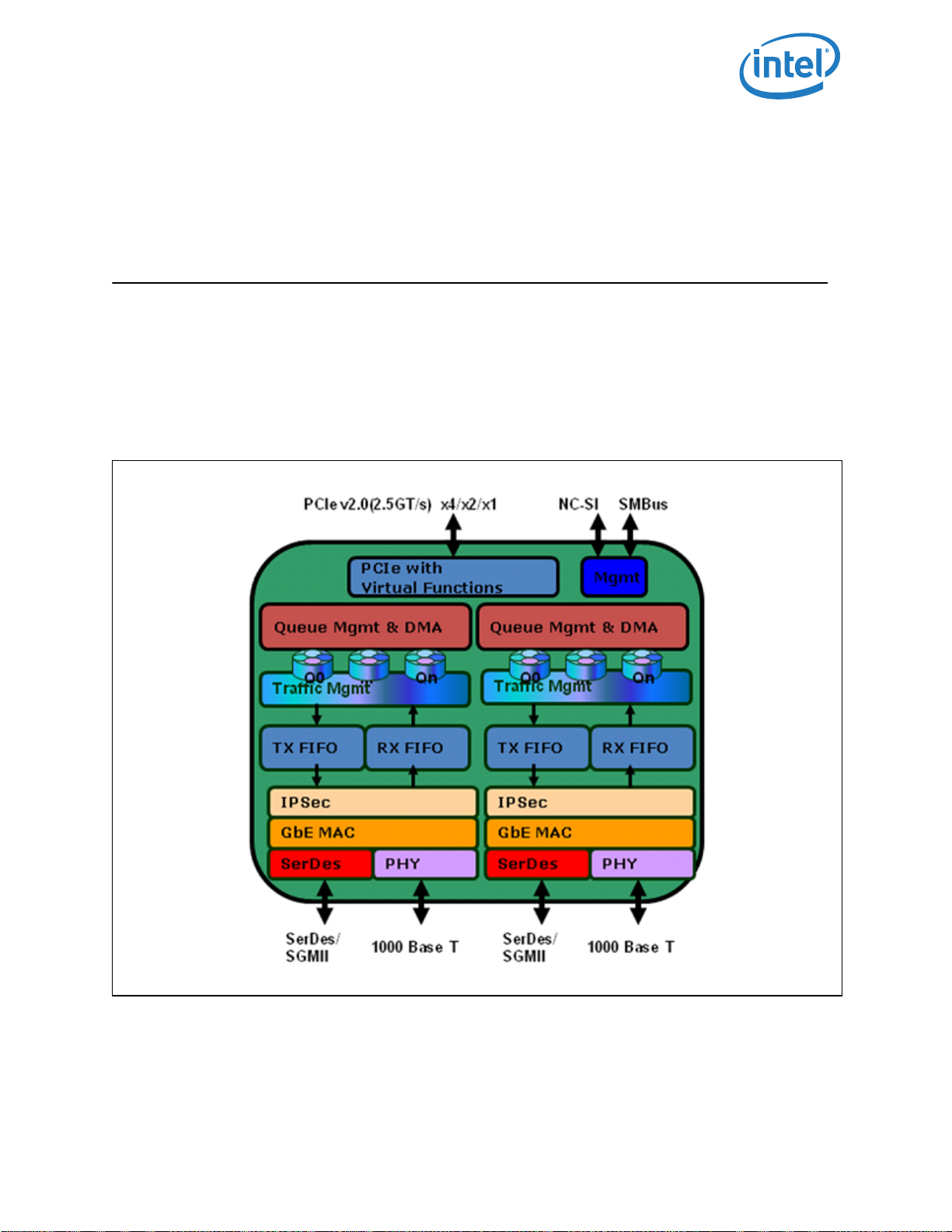
Introduction — Intel® 82576EB GbE Controller
1.0 Introduction
The Intel® 82576 GbE Controller is a single, compact, low power component that offers two fullyintegrated Gigabit Ethernet Media Access Control (MAC) and physical layer (PHY) ports. This device
uses the PCIe* v2.0 (2.5GT/s). The 82576 enables two-port implementation in a relatively small area
and can be used for server system configurations such as rack mounted or pedestal servers, where the
82576 can be used as add-on NIC or LAN on Motherboard (LOM) design. Another system configuration
is blade servers, where it can be used as LOM. The 82576 can also be used in embedded applications
such as switch add-on cards and network appliances.
Figure 1-1. 82576 Block Diagram
®
Revision: 2.63 Intel
December 2011 Datasheet
43
82576EB GbE Controller
Page 44

Intel® 82576EB GbE Controller — Introduction
1.1 Scope
This document presents the external architecture (including device operation, pin descriptions, register
definitions, etc.) for the 82576, a dual 10/100/1000 LAN controller.
This document is intended to be a reference for software device driver developers, board designers,
test engineers, or others who may need specific technical or programming information.
1.2 Terminology and Acronyms
Table 1-1. Glossary
Definition Meaning
1000BASE-BX 1000BASE-BX is the PICMG 3.1 electrical specification for
1000BASE-CX 1000BASE-X over specialty shielded 150 balanced copper
1000BASE-T 1000BASE-T is the specification for 1 Gb/s Ethernet over
AH IP Authentication Header - An IPsec header providing
b/w Bandwidth.
BIOS Basic Input/Output System.
BMC Baseboard Management Controller.
BT Byte Time.
BWG Bandwidth Group.
CA Secure Connectivity Association (CA): A security relationship,
CPID Congestion Point Identifier.
CTS Cisco Trusted Security
transmission of
1 Gb/s Ethernet or 1 Gb/s fibre channel encoded data over the
backplane.
jumper cable assemblies as specified in IEEE 802.3 Clause 39.
category 5e twisted pair cables as defined in IEEE 802.3
clause 40.
authentication capabilities defined in RFC 4302.
established and maintained by key agreement protocols. This
comprises a fully connected subset of the service access
points in stations attached to a single LAN that are to be
supported by MACSec.
1
DCA Intel® QuickData (Direct Cache Access).
DFP Deficit Fixed Priority.
DFT Design for Testability.
DQ Descriptor Queue.
EEPROM Electrically Erasable Programmable Memory. A non-volatile
EOP End of Packet.
Intel® 82576EB GbE Controller Revision: 2.63
Datasheet December 2011
44
memory located on the LAN controller that is directly
accessible from the host.
Page 45

Introduction — Intel® 82576EB GbE Controller
Table 1-1. Glossary (Continued)
Definition Meaning
ESP IP Encapsulating Security Payload - An IPsec header providing
encryption and authentication capabilities defined in RFC
1
4303.
FC Flow Control.
Firmware (FW) Embedded code on the LAN controller that is responsible for
the implementation of the NC-SI protocol and pass through
functionality.
Host Interface RAM on the LAN controller that is shared between the
firmware and the host. RAM is used to pass commands from
the host to firmware and responses from the firmware to the
host.
HPC High - Performance Computing.
IPC Inter Processor Communication.
IPG Inter Packet Gap.
LAN (auxiliary Power-Up) The event of connecting the LAN controller to a power source
(occurs even before system power-up).
LOM LAN on Motherboard.
LSO Large Send Offload.
MAC Media Access Control.
MDIO Management Data Input/Output Interface over MDC/MDIO
lines.
MIFS/MIPG Minimum Inter Frame Spacing/Minimum Inter Packet Gap.
MMW Maximum Memory Window.
MSS Maximum Segment Size.
NIC Network Interface Controller.
PCS Physical Coding Sub layer.
PF Physical Function (in a virtualization context).
PHY Physical Layer Device.
PMA Physical Medium Attachment.
PMD Physical Medium Dependent.
PN (in a MACSec context) packet number (PN): A monotonically increasing value used to
uniquely identify a MACSec frame in the sequence of frames
transmitted using an SA.
NC-SI (Type C) Reduced Media Independent Interface (Reduced MII).
SA Source Address.
SA (in a MACSec context) Secure Association (SA): A security relationship that provides
security guarantees for frames transmitted from one member
of a CA to the others. Each SA is supported by a single secret
key, or a single set of keys where the cryptographic
operations used to protect one frame require more than one
key.
®
Revision: 2.63 Intel
82576EB GbE Controller
December 2011 Datasheet
45
Page 46

Table 1-1. Glossary (Continued)
Definition Meaning
Intel® 82576EB GbE Controller — Introduction
SC Secure Channel (SC): A security relationship used to provide
SCI A globally unique identifier for a secure channel, comprising a
SDP Software Defined Pins.
SerDes Serializer and De-Serializer Circuit.
SFD Start Frame Delimiter.
SGMII Serialized Gigabit Media Independent Interface.
SMBus System Management Bus. A bus that carries various
TRL Transmit Rate Limiting or Transmit Rate Limiter, according to
TSO Transmit Segmentation offload - A mode in which a large TCP/
VF Virtual Function.
VM Virtual Machine.
VPD Vital Product Data (PCI protocol).
security guarantees for frames transmitted from one member
of a CA to the others. An SC is supported by a sequence of
SAs thus allowing the periodic use of fresh keys without
terminating the relationship.
globally unique MAC Address and a Port Identifier, unique
within the system allocated that address.
manageability components, including the LAN controller,
BIOS, sensors and remote-control devices.
the context.
UDP I/O is handled to the device and the device segments it
to L2 packets according to the requested MSS.
1. The IPsec function is present in the 82576EB SKU. IPsec is removed from the 82576NS SKU.
1.2.1 External Specification and Documents
The 82576 implements features from the following specifications.
1.2.1.1 Network Interface Documents
1. IEEE standard 802.3, 2005 Edition (Ethernet). Incorporates various IEEE Standards previously
published separately. Institute of Electrical and Electronic Engineers (IEEE).
2. IEEE standard 1149.1, 2001 Edition (JTAG). Institute of Electrical and Electronics Engineers (IEEE)
3. IEEE standard 802.1Q for VLAN
4. PICMG3.1 Ethernet/Fibre Channel Over PICMG 3.0 Draft Specification January 14, 2003 Version
D1.0
5. Serial-GMII Specification, Cisco Systems document ENG-46158, Revision 1.7.
6. INF-8074i Specification for SFP (Small Formfactor Pluggable) Transceiver (ftp://ftp.seagate.com/
sff)
Intel® 82576EB GbE Controller Revision: 2.63
Datasheet December 2011
46
Page 47

Introduction — Intel® 82576EB GbE Controller
1.2.1.2 Host Interface Documents
1. PCI-Express 2.0 Base specification, Revision 1.0
2. PCI Specification, version 3.0
3. PCI Bus Power Management Interface Specification, Rev. 1.2, March 2004
4. Advanced Configuration and Power Interface Specification, Rev 2.0b, October 2002
1.2.1.3 Virtualization Documents
1. PCI-Express Single Root I/O Virtualization and Sharing Specification rev 0.9
2. PCI sig Alternative Routing-ID Interpretation (ARI) ECN
PASDPA/PCIe/PCI%20Express%20Product_Spec%20Coordination/pages/
PCISIG%20WIP%20Docs.aspx)
(http://teamsites.ch.ith.intel.com/sites/
1.2.1.4 Networking Protocol Documents
1. IPv4 specification (RFC 791)
2. IPv6 specification (RFC 2460)
3. TCP/UDP specification (RFC 793/768)
4. SCTP specification (RFC 2960)
5. ARP specification (RFC 826)
6. EUI-64 specification, http://standards.ieee.org/regauth/oui/tutorials/EUI64.html.
1.2.1.5 Manageability documents
1. DMTF Network Controller Sideband Interface (NC-SI) Specification rev 0.7. This product is Type C.
2. System Management Bus (SMBus) Specification, SBS Implementers Forum, Ver. 2.0, August 2000
1.2.1.6 Security Documents
1. IEEE P802.1AE/D5.1 — Draft Standard for Local and Metropolitan Area Networks — Media Access
Control (MAC) Security.
2. The Use of Galois/Counter Mode (GCM) in IPsec Encapsulating Security Payload (ESP) (RFC 4106)
3. IP Authentication Header (AH) (RFC 4302)
4. IP Encapsulating Security Payload (ESP) (RFC 4303)
5. The Use of Galois Message Authentication Code (GMAC) in IPsec ESP and AH (RFC 4543).
1.2.2 Intel Application Notes
1. Intel® Ethernet Controllers Loopback Modes - application note.
1.2.3 Reference Schematics
Reference schematics (SERDES\FIBER\SFP and COPPER) are available as a separate document through
Intel documentation channels.
®
Revision: 2.63 Intel
December 2011 Datasheet
47
82576EB GbE Controller
Page 48

Intel® 82576EB GbE Controller — Introduction
1.2.4 Checklists
The Schematic Checklist and the Layout and Placement Checklist are available as a separate document
through Intel documentation channels.
1.3 Product Overview
The 82576 supports 2 ports with either an internal PHY or a SerDes or SGMII port which may connected
to an external PHY or directly to a blade connection for MAC to MAC communication.
1.3.1 System Configurations
The 82576 targets server system configurations such as rack mounted or pedestal servers, where the
82576 can be used as add-on NIC or LAN on Motherboard (LOM) design. Another system configuration
is blade servers, where it can be used as LOM. The 82576 can also be used in embedded applications
such as switch add-on cards and network appliances.
1.4 External Interface
1.4.1 PCIe* Interface
The PCIe v2.0 (2.5GT/s) interface is used by the 82576 as a host interface. It supports x4, x2 and x1
configurations, while each lane runs at 2.5 GHz speed. The maximum aggregated raw bandwidth for a
typical x4 configuration is 8 Gb/s in each direction. See Chapter 2.0 for a full description. The timing
characteristics of this interface are defined in PCI Express Card Electromechanical Specification rev 1.0
and in the PCIe v2.0 (2.5GT/s) specification.
1.4.2 Network interfaces
Two independent interfaces are used to connect the two 82576 ports to external devices. The following
protocols are supported:
• 10BASE-T and 100BASE-T.
• 1000Base-T interface to attach directly to a CAT 5e wire.
• SerDes interface to connect over a backplane to another SerDes compliant device or to an optic
module.
• SGMII interface to attach to an external PHY, either on board or via an SFP module. The SGMII
shares the same interface as the SerDes.
• MDI (Copper) support for standard IEEE 802.3 Ethernet interface for 1000BASE-T, 100BASE-TX,
and 10BASE-T applications (802.3, 802.3u, and 802.3ab).
See Section 2.1.8.2 and Section 2.1.6 for full pin description; Section 11.4.4.1 to Section 11.4.4.3 for
timing characteristics of this interface.
Intel® 82576EB GbE Controller Revision: 2.63
Datasheet December 2011
48
Page 49

Introduction — Intel® 82576EB GbE Controller
1.4.3 EEPROM Interface
The 82576 uses an EEPROM device for storing product configuration information. Several words of the
EEPROM are accessed automatically by the 82576 after reset in order to provide pre-boot configuration
data that must be available to the 82576 before it is accessed by host software. The remainder of the
stored information is accessed by various software modules used to report product configuration, serial
number, etc.
The 82576 is intended for use with an SPI (4-wire) serial EEPROM device such as an AT25040AN or
compatible. See Section 2.1.2 for full pin description and Section 11.4.3.5 for timing characteristics of
this interface.
The 82576 also supports an EEPROM-less mode, where all of the setup is done by software.
1.4.4 Serial Flash Interface
The 82576 provides an external SPI serial interface to a Flash or Boot ROM device such as the Atmel*
AT25F1024 or AT25FB512. The 82576 supports serial Flash devices with up to 64 Mb (8 MB) of
memory. The size of the Flash used by the 82576 can be configured by the EEPROM. See Section 2.1.2
for full pin description and Section 11.4.3.4 for timing characteristics of this interface.
Note: Though the 82576 supports devices with up to 8 MB of memory, bigger devices can also be
used. Accesses to memory beyond the Flash device size results in access wrapping as only
the lower address bits are used by the Flash device.
1.4.5 SMBus Interface
SMBus is an optional interface for pass-through and/or configuration traffic between a MC and the
82576.
The 82576's SMBus interface can be configured to support both slow and fast timing modes. See
Section 2.1.3 for full pin description and Section 11.4.3.3 for timing characteristics of this interface.
1.4.6 NC-SI Interface
NC-SI and SMBus interfaces are optional for pass-through and/or configuration traffic between a MC
and the 82576. The NC-SI interface meets the DMTF NC-SI Specification, Rev. 1.0.0.a.
1.4.7 MDIO/2 wires Interfaces
The 82576 implements two management Interfaces for control of an optional external PHY. Each
interface can be either a 2 wires interface used to control an SFP module or MDIO/MDC Management
Interface for control plane connection between the MAC and PHY devices (master side). This interface
provides the MAC and software with the ability to monitor and control the state of the PHY. The 82576
supports the data formats of 802.3 clause 22. Each MDIO interface should be connected to the relevant
PHY.
See Section 2.1.7 for full pin description and Section 11.4.3.9 for timing characteristics of this
interface.
®
Revision: 2.63 Intel
December 2011 Datasheet
49
82576EB GbE Controller
Page 50

Intel® 82576EB GbE Controller — Introduction
1.4.8 Software-Definable Pins (SDP) Interface (General-Purpose I/O)
The 82576 has four software-defined pins (SDP pins) per port that can be used for miscellaneous
hardware or software-control purposes. These pins can be individually configurable to act as either
input or output pins. The default direction of each pin is configurable via the EEPROM (see Section 6.2.8
and Section 6.2.9), as well as the default value of all pins configured as outputs. To avoid signal
contention, all pins are set as input pins until the EEPROM configuration is loaded. All four of the SDP
pins can be configured for use as general-purpose interrupt (GPI) inputs. To act as GPI pins, the desired
pins must be configured as inputs. A corresponding GPI interrupt-detection enable bit is then used to
enable rising-edge detection of the input pin (rising-edge detection occurs by comparing values
sampled at the internal clock rate, as opposed to an edge-detection circuit). When detected, a
corresponding GPI interrupt is indicated in the Interrupt Cause register.
The use, direction, and values of SDP pins are controlled and accessed using fields in the Device Control
(CTRL) register and Extended Device Control (CTRL_EXT) register.
See Section 2.1.5 for full pin description of this interface.
1.4.9 LEDs Interface
The 82576 implements four output drivers per port intended for driving external LED circuits. Each of
the four LED outputs can be individually configured to select the particular event, state, or activity,
which is indicated on that output. In addition, each LED can be individually configured for output
polarity as well as for blinking versus non-blinking (steady-state) indication.
The configuration for LED outputs is specified via the LEDCTL register. Furthermore, the hardwaredefault configuration for all LED outputs can be specified via EEPROM fields (see Section 6.2.19 and
Section 6.2.21), thereby supporting LED displays configurable to a particular OEM preference.
See Section 2.1.8.1 for full pin description of this interface.
See Section 7.5 for more detailed description of LED behavior.
1.5 Comparing Product Features
The following tables compare features of similar Intel components.
Table 1-2. 82576 Features
Feature 82576 82575 82571EB
Number of ports 222
Serial FLASH interface Y Y Y
4-wire SPI EEPROM interface Y Y Y
Configurable LED operation for software or OEM custom-tailoring of LED
displays
Protected EEPROM space for private configuration Y Y Y
YYY
Intel® 82576EB GbE Controller Revision: 2.63
Datasheet December 2011
50
Page 51

Introduction — Intel® 82576EB GbE Controller
Table 1-2. 82576 Features (Continued)
Device Disable capability Y Y Y
Package size (mm x mm) 25x25 25x25 17x17
Watchdog timer YYN
Table 1-3. 82576 Network Features
Feature 82576 82575 82571EB
Half duplex at 10/100 Mb/s operation and full duplex operation at all
supported speeds
10/100/1000 Copper PHY integrated on-chip Y Y Y
Jumbo frames supported Y Y Y
Max size of jumbo frames supported 9500
Flow control support: send/receive PAUSE frames and receive FIFO
thresholds
Statistics for management and RMON Y Y Y
802.1q VLAN support Y Y Y
SerDes interface for external PHY connection or system interconnect Y Y Y
SGMII interface for embedded applications Y Y N
Fiber/copper auto-sense* Y Y N
SerDes support of non-Auto-Negotiation partner Y Y N
SerDes signal detect Y Y N
*
YYY
bytes
YYY
9500
bytes
Table 1-4. 82576 Host Interface Features (Sheet 1 of 2)
Feature 82576 82575 82571EB
9000
bytes
PCIe revision 2.0 2.0 1.0a
PCIe physical layer (2.5 GT/s) 2.5 GT/
Bus width x1, x2, x4 x1, x2, x4x1, x2, x4
64-bit address support for systems using more than
4 GB of physical memory
Outstanding requests for Tx buffers 4 4 4
Outstanding requests for Tx descriptors 1 1 1
Outstanding requests for Rx descriptors 1 1 1
Credits for posted writes 2 2 2
Max payload size supported 512 B 256 B 256 B
Revision: 2.63 Intel
December 2011 Datasheet
51
YY Y
s)
2.5 GT/s)
®
82576EB GbE Controller
Page 52

Intel® 82576EB GbE Controller — Introduction
Table 1-4. 82576 Host Interface Features (Sheet 2 of 2)
Max request size supported 512 B 512 B 256 B
Link layer retry buffer size 2 KB 2 KB 2 KB
Vital Product Data (VPD) Y N N
Table 1-5. 82576 LAN Functions Features
Feature 82576 82575 82571EB
Programmable host memory receive buffers Y Y Y
Descriptor ring management hardware for transmit and receive Y Y Y
ACPI register set and power down functionality supporting D0 & D3
states
Software controlled global reset bit (resets everything except the
configuration registers)
Software Definable Pins (SDP) - per port 4 4 4
Four SDP pins can be configured as general purpose interrupts Y Y Only 2
Wake up YY Y
IPv6 wake-up filters Y Y Y
Configurable (through the EEPROM) flexible filter Y Y Y
Default configuration by the EEPROM for all LEDs for pre-driver
functionality
LAN function disable capability Y Y Y
Programmable memory transmit buffers (up to 32 KB) Y Y Y
Double VLAN YY N
IEEE 1588 YN N
YY Y
YY Y
YY Y
Table 1-6. 82576 LAN Performance Features
Feature 82576 82575 82571EB
TCP segmentation offload
Up to 256 KB
YY Y
Transmit Rate Limiting (TRL) Y N N
IPv6 support for IP/TCP and IP/UDP receive checksum offload Y Y Y
Fragmented UDP checksum offload for packet reassembly Y Y Y
Message Signaled Interrupts (MSI) Y Y Y
Message Signaled Interrupts (MSI-X) Y Y N
Packet interrupt coalescing timers (packet timers) and absolutedelay interrupt timers for both transmit and receive operation
Interrupt throttling control to limit maximum interrupt rate and
improve CPU utilization
Intel® 82576EB GbE Controller Revision: 2.63
Datasheet December 2011
52
YN N
YY Y
Page 53

Introduction — Intel® 82576EB GbE Controller
Table 1-6. 82576 LAN Performance Features
Rx packet split header Y Y Y
Receive Side Scaling (RSS) number of queues Up to 16 4 2
Total number of RX queues per port 16 4 2
Total number of TX queues per port 16 4 2
RX header replication
Low latency interrupt
DCA support
TCP timer interrupts
No snoop
Relax ordering
TSO interleaving for reduced latency Y N N
Receive side coalescing N N N
SCTP receive and transmit checksum offload Y N N
UDP TSO YN N
Yes to all Yes to
all
Y
N
N
N
Y
Y
Table 1-7. 82576 Virtualization Features
Feature 82576 82575 82571EB
Support for Virtual Machines Device queues (VMDq) 8 pools 4 N
PCI-SIG SR IOV 8 VF N N
Multicast/Broadcast Packet replication Y N N
VM to VM Packet forwarding Y N N
Traffic shaping Y N N
MAC addresses 24 16 15
MAC and VLAN anti-spoofing Y N N
VLAN filtering Per pool Global Global
Per-pool statistics Y N N
Per-pool off loads Y Partial N
Per-pool jumbo support Y N N
Mirroring rules 4 0 0
Table 1-8. 82576 Manageability Features
Feature 82576 82575 82571EB
Advanced pass-through-compatible management packet transmit/
receive support
Manageability support for ASF 1.0 and Alert on LAN 2.0 N Y Y
Revision: 2.63 Intel
December 2011 Datasheet
53
YY Y
®
82576EB GbE Controller
Page 54

Intel® 82576EB GbE Controller — Introduction
Table 1-8. 82576 Manageability Features (Continued)
SMBus interface to external BMC Y Y Y
DMTF NC-SI protocol standards support Y Y N
L2 address filters 4 4 1
VLAN L2 filters 8 8 4
Flex L3 port filters 16 16 3
Flex TCO filters 4 4 2
L3 address filters (IPv4) 4 4 4
L3 address filters (IPv6) 4 4 1
Table 1-9. 82576 Security Features
Feature 82576 82575 82571EB
Integrated MACSec security engines
• GCM AES 128 encryption or authentication engine.
• One Secure Connection
• Two Security associations.
• Replay protection with zero window.
Integrated IPSec Offload Engine
• Security Associations - Rx
• Security Associations - Tx
• IP Authentication Header (AH) protocol
• IP Encapsulating Security Payload (ESP) for authentication and/or
Encryption.
• AES-128-GMAC (128-bit key) engine
• IPv4 and IPv6 support (without options or extensions)
1. IPsec functionality is present in the 82576EB SKU. IPsec is removed from the 82576NS SKU.
*
1
YNN
Y
256
256
Y
Y
Y
Y
NN
1.6 Overview of New Capabilities
The following section describes features added in Intel® 82576 GbE Controller that are new related to
82575.
1.6.1 IPsec Off Load for Flows
Note: The IPsec function is present in the 82576EB SKU. IPsec is removed from the 82576NS
SKU.
The 82576 (SKU: 82576EB) supports IPsec off load for a given number of flows. It is the operating
system’s responsibility to submit to hardware the most loaded flows, in order to take maximum
benefits of the IPsec off-load in terms of CPU utilization savings. Main features are:
Intel® 82576EB GbE Controller Revision: 2.63
Datasheet December 2011
54
Page 55

Introduction — Intel® 82576EB GbE Controller
• Off-load IPsec for up to 256 Security Associations (SA) for each of Tx and Rx.
• AH and ESP protocols for authentication and encryption
AES-128-GMAC and AES-128-GCM crypto engines:
• Transport mode encapsulation
• IPv4 and IPv6 versions (no options or extension headers)
1.6.2 Security
The 82576 supports the IEEE 802.1ae specification. It incorporates an inline packet crypto unit to
support both privacy and integrity checks on a packet by packet basis. The transmit data path includes
both encryption and signing engines. On the receive data path, the 82576 includes a decryption engine
and an integrity checker. The crypto engines use an AES GCM algorithm that is designed to support the
802.1ae protocol. Note that both host traffic and MC management traffic might be subjected to
authentication and/or encryption.
1.6.3 Transmit Rate Limiting (TRL)
The 82576 supports the ability to limit the transmiting rate. TRL can be enabled for each transmit
queue. The following modes of TRL are used:
• Frame Overhead — IPG is extended by a fixed value for all transmit queues.
• Payload Rate — IPG, stretched relative to frame size, provides pre-determined data (bytes) rates
for each transmit queue.
1.6.4 Performance
The 82576 improvements include:
• Latency - The 82576 reduces end-to-end latency for high priority traffic in presence of other traffic.
Specifically, the 82576 reduces the delay caused by preceding TSO packets.
• CPU Utilization - The 82576 supports reducing CPU utilization in a virtualized system by
incorporating enhancements to the VMDq feature.
1.6.4.1 Tx Descriptor Write-Back
This functionality is an improvement to the way Tx descriptors are written back to memory. Instead of
writing back the DD bit into the descriptor location, the head pointer is updated in system memory. The
head pointer is updated based on the RS bit or prior to expiration of the corresponding interrupt vector.
1.6.5 Rx and Tx Queues
The number of Tx and Rx queues in the 82576 was increased to 16 queues.
1.6.6 Interrupts
The following changes in the interrupt scheme are implemented in the 82576:
• Rate controlling of low latency interrupts
®
Revision: 2.63 Intel
December 2011 Datasheet
55
82576EB GbE Controller
Page 56

Intel® 82576EB GbE Controller — Introduction
• Extensions to the low latency interrupt filters to enable immediate interrupt by full 5-tuple
matching
1.6.7 Virtualization
1.6.7.1 PCI SR IOV
The 82576 supports the PCI-SIG Single-Root I/O Virtualization and Sharing specification (SR-IOV),
including the following functionality:
• Support for up to 8 virtual functions.
• Partial replication of PCI configuration space
• Allocation of MMIO space per virtual function
• Allocation of a requester ID per virtual function
• Virtualization of interrupts
1.6.7.2 Packets Classification
Received unicast packets are forwarded to the appropriate VM queue based on their unicast L2 address.
Broadcast and Multicast (MC) packets, however, might need to be forwarded to multiple VMs. Multicast
is commonly used to share information among a group of systems.
Received MC packets are forwarded to their destination VMs based on mapping between the MC
address and the target VMs.
Broadcast packets that are VLAN tagged are forwarded to destination VMs based on their VLAN tag.
Note that a VM might be associated with multiple VLAN addresses. A broadcast packet that is not VLAN
tagged can be optionally forwarded to all VMs.
Packet forwarding services inter-VM communication by forwarding transmit packets from a transmit
queue to an Rx software queue. The motivation to execute packet forwarding in the 82576 is in direct
assignment architecture, where it is desired that a guest VM interacts directly with the 82576 using a
standard device driver. If packet forwarding is to be done by system software, the guest VM (its device
driver) needs to filter local packets and forward those to a software switch to forward.
Transmit packets with a local destination are classified based on the same criteria as packets received
from the wire.
1.6.7.3 Hardware Virtualization
This section covers replication of hardware resources beyond the scope of PCI resources handled by PCI
SR-IOV. The following features are supported:
• Interrupts – part of the interrupts are assigned per VM.
• Statistics – enable read access to VMs in direct assignment model without the clear-on-read side
effect.
• Storm control - if an unusually high bandwidth of broadcast or multicast packets is detected, the
82576 can be configured to drop broadcast or multicast packets until the storm condition is over.
• Security features: VLAN and MAC anti-spoof are supported as well as insertion of VLAN according to
the physical function control.
Intel® 82576EB GbE Controller Revision: 2.63
Datasheet December 2011
56
Page 57

Introduction — Intel® 82576EB GbE Controller
1.6.7.4 Bandwidth Allocation
The 82576 allows allocation of transmit bandwidth among the virtual interfaces to avoid unfair use of
bandwidth by a single VM.
1.6.8 VPD
The 82576 supports the Vital Product Data (VPD) capability defined in the PCI Specification, version
3.0.
1.6.9 64 bit BARs support
The 82576 supports different configuration of the I/O and MMIO Base Address Registers to allow
support of 64 bit mappings of BARs.
1.6.10 IEEE 1588 - Precision Time Protocol (PTP)
The IEEE 1588 International Standard enables networked Ethernet equipment to synchronize internal
clocks according to a network master clock. The protocol is implemented in software, with the 82576
providing accurate time measurements of special Tx and Rx packets close to the Ethernet link. These
packets measure the latency between the master clock and an end-point clock in both link directions.
The endpoint can then acquire an accurate estimate of the master time by compensating for link
latency.
The 82576 provides the following support for the IEEE 1588 protocol:
• Detection of specific PTP Rx packets and capturing the time of arrival of such packets in dedicated
CSRs
• Detection of specific PTP Tx packets and capturing the time of transmission of such packets in
dedicated CSRs
• A software-visible reference clock for the previously mentioned time captures.
• Both the L2 based and the UDP based version of the protocol are supported.
• Generation of an external clock on one of the SDPs.
• Triggering of external devices based on internal clock.
• Timestamps of external events.
1.7 Device Data Flows
1.7.1 Transmit Data Flow
Tx data flow provides a high level description of all data/control transformation steps needed for
sending Ethernet packets to the line.
®
Revision: 2.63 Intel
December 2011 Datasheet
57
82576EB GbE Controller
Page 58

Table 1-10. Transmit Data Flow
Step Description
Intel® 82576EB GbE Controller — Introduction
1 The host creates a descriptor ring and configures one of the 82576's transmit queues with the address location,
2 The host is requested by the TCP/IP stack to transmit a packet, it gets the packet data within one or more data
3 The host initializes descriptor(s) that point to the data buffer(s) and have additional control parameters that
4 The host updates the appropriate queue tail pointer (TDT)
5 The 82576's DMA senses a change of a specific TDT and as a result sends a PCIe request to fetch the
6 The descriptor(s) content is received in a PCIe read completion and is written to the appropriate location in the
7 The DMA fetches the next descriptor from the internal cache and processes its content. As a result, the DMA
8 The packet data is received from PCIe completions and passes through the transmit DMA that performs all
9 While the packet is passing through the DMA, it is stored into the transmit FIFO. After the entire packet is
10 If the packet destination is also local, it is sent also to the local switch memory and join the receive path.
11 The transmit switch arbitrates between host and management packets and eventually forwards the packet to
12 The security engine optionally applies L3 (IPsec) or L2 (MACSec) encryption or authentication and forwards the
length, head and tail pointers of the ring (one of 16 available Tx queues).
buffers.
describe the needed hardware functionality. The host places that descriptor in the correct location at the
appropriate Tx ring.
descriptor(s) from host memory.
descriptor queue internal cache.
sends PCIe requests to fetch the packet data from system memory.
programmed data manipulations (various CPU off loading tasks as checksum off load, TSO off load, etc.) on the
packet data on the fly.
stored in the transmit FIFO, it is forwarded to the transmit switch module.
the Security engine.
packet to the MAC.
13 The MAC appends the L2 CRC to the packet and sends the packet to the line using a pre-configured interface.
14 When all the PCIe completions for a given packet are done, the DMA updates the appropriate descriptor(s).
15 After enough descriptors are gathered for write back or the interrupt moderation timer expires, the descriptors
16 After the interrupt moderation timer expires, an interrupt is generated to notify the host device driver that the
are written back to host memory using PCIe posted writes. Alternatively, the head pointer can only be written
back.
specific packet has been read to the 82576 and the driver can release the buffers.
1.7.2 Receive Data Flow
Receive (Rx) data flow provides a high level description of all data/control transformation steps needed
for receiving Ethernet packets.
Table 1-11. Receive Data Flow
Step Description
1 The host creates a descriptor ring and configures one of the 82576's receive queues with the address location,
2 The host initializes descriptors that point to empty data buffers. The host places these descriptors in the correct
Intel® 82576EB GbE Controller Revision: 2.63
Datasheet December 2011
58
length, head, and tail pointers of the ring (one of 16 available Rx queues).
location at the appropriate Rx ring.
Page 59

Introduction — Intel® 82576EB GbE Controller
Table 1-11. Receive Data Flow (Continued)
3 The host updates the appropriate queue tail pointer (RDT).
4 The 82576's DMA senses a change of a specific RDT and as a result sends a PCIe request to fetch the
5 The descriptors content is received in a PCIe read completion and is written to the appropriate location in the
6 A packet enters the Rx MAC. The RX MAC checks the CRC of the packet.
7 The MAC forwards the packet to an Rx filter
8 If the packet is a MACSec or an IPSec packet and the adequate key is stored in the hardware, the packet is
9 If the packet matches the pre-programmed criteria of the Rx filtering, it is forwarded to the Rx FIFO. VLAN and
10 The receive DMA fetches the next descriptor from the internal cache of the appropriate queue to be used for the
11 After the entire packet is placed into the Rx FIFO, the receive DMA posts the packet data to the location
12 When the packet is placed into host memory, the receive DMA updates all the descriptor(s) that were used by
12 After enough descriptors are gathered for write back or the interrupt moderation timer expires or the packet
13 After the interrupt moderation timer completes or an immediate packet is received, the 82576 initiates an
descriptors from host memory.
descriptor queue internal cache.
decrypted and authenticated.
CRC are optionally stripped from the packet and L3/L4 checksum are checked and the destination queue is
fixed.
next received packet.
indicated by the descriptor through the PCIe interface. If the packet size is greater than the buffer size, more
descriptors are fetched and their buffers are used for the received packet.
packet data.
requires immediate forwarding, the receive DMA writes back the descriptor content along with status bits that
indicate the packet information including what off loads were done on that packet.
interrupt to the host to indicate that a new received packet is already in host memory.
14 Host reads the packet data and sends it to the TCP/IP stack for further processing. The host releases the
associated buffers and descriptors once they are no longer in use.
§ §
®
Revision: 2.63 Intel
December 2011 Datasheet
59
82576EB GbE Controller
Page 60

NOTE: This page intentionally left blank.
Intel® 82576EB GbE Controller — Introduction
Intel® 82576EB GbE Controller Revision: 2.63
Datasheet December 2011
60
Page 61

Pin Interface — Intel® 82576EB GbE Controller
2.0 Pin Interface
2.1 Pin Assignment
The 82576 is packaged in 25mmx25mm FCBGA package with 1 mm ball pitch.
Table 2-1. Signal Type Definition
Type Description DC specification
In Input is a standard input-only signal. See Section 11.4.2.2
Out Totem Pole Output is a standard active driver. See Section 11.4.2.2
T/S Tri-State is a bi-directional, tri-state input/output
pin.
O/D Open Drain allows multiple devices to share as a
wire-OR.
NC-SI-in Input signal See Section 11.4.2.4
NC-SI-out Output signal See Section 11.4.2.4
A Analog PHY signals See Section 11.4.5
A-in Analog input signals See Section 11.4.4
A-out Analog output signals See Section 11.4.4
B Input bias See Section 11.4.7
See Section 11.4.2.2
See Section 11.4.2.3
2.1.1 PCIe
The AC specification for these pins is described in Chapter 11.0.
Table 2-2. PCI* Pins
Symbol Ball # Type Name and Function
PE_CLK_p
PE_CLK_n
PET_0_p
PET_0_n
N2
N1
D2
D1
A-in PCIe* Differential Reference Clock in: A 100MHz differential clock input. This clock
Aout
is used as the reference clock for the PCIe* Tx/Rx circuitry and by the PCIe* core
PLL to generate clocks for the PCIe* core logic.
PCIe* Serial Data output: A serial differential output pair running at 2.5Gb/s. This
output carries both data and an embedded 2.5GHz clock that is recovered along
with data at the receiving end.
PET_1_p
PET_1_n
Revision: 2.63 Intel
December 2011 Datasheet
61
H2
H1
Aout
PCIe* Serial Data output: A serial differential output pair running at 2.5Gb/s. This
output carries both data and an embedded 2.5GHz clock that is recovered along
with data at the receiving end.
®
82576EB GbE Controller
Page 62

Table 2-2. PCI* Pins (Continued)
PET_2_p
PET_2_n
R2
R1
Aout
PCIe* Serial Data output: A serial differential output pair running at 2.5Gb/s. This
output carries both data and an embedded 2.5GHz clock that is recovered along
with data at the receiving end.
Intel® 82576EB GbE Controller — Pin Interface
PET_3_p
PET_3_n
PER_0_p
PER_0_n
PER_1_p
PER_1_n
PER_2_p
PER_2_n
PER_3_p
PER_3_n
PE_WAKE_N AC20 O/D WAKE: Pulled to ‘0’ to indicate that a Power Management Event (PME) is pending
PE_RST_N AC9 In Power and Clock Good Indication: Indicates that power and PCI Express reference
RSVDM3_NC
RSVDM2_NC
PE_RCOMP L1 B Impedance compensation. Connect to ground through an external 1.4 Kohm 1%
W2
W1
F2
F1
K2
K1
U2
U1
AA2
AA1
M3
M2
Aout
A-in PCIe* Serial Data input: A Serial differential input pair running at 2.5Gb/s. An
A-in PCIe* Serial Data input: A Serial differential input pair running at 2.5Gb/s. An
A-in PCIe* Serial Data input: A Serial differential input pair running at 2.5Gb/s. An
A-in PCIe* Serial Data input: A Serial differential input pair running at 2.5Gb/s. An
Aout
PCIe* Serial Data output: A serial differential output pair running at 2.5Gb/s. This
output carries both data and an embedded 2.5GHz clock that is recovered along
with data at the receiving end.
embedded clock present in this input is recovered along with the data.
embedded clock present in this input is recovered along with the data.
embedded clock present in this input is recovered along with the data.
embedded clock present in this input is recovered along with the data.
and the PCI Express link should be restored. Defined in the PCI Express
specifications.
clock are within specified values. Defined in the PCI Express specifications.
This pin is used as a fundamental reset indication for the device.
Analog testing
100ppm resistor for impedance compensation. See Figure 11-13 for details.
2.1.2 Flash and EEPROM Ports (8)
The AC specification for these pins is described in Section 11.4.3.4 to Section 11.4.3.5.
Table 2-3. Flash and EEPROM Ports
Symbol Ball # Type Name and Function
FLSH_SI AC14 T/S Serial Data output to the Flash
FLSH_SO AD14 In Serial Data input from the Flash
FLSH_SCK AD15 T/S Flash serial clock Operates at ~20MHz.
FLSH_CE_N AC15 T/S Flash chip select Output
EE_DI A21 T/S Data output to EEPROM
EE_DO A20 In Data input from EEPROM
EE_SK B20 T/S EEPROM serial clock Operates at ~2MHz.
EE_CS_N B21 T/S EEPROM chip select Output
Intel® 82576EB GbE Controller Revision: 2.63
Datasheet December 2011
62
Page 63

Pin Interface — Intel® 82576EB GbE Controller
2.1.3 System Management Bus (SMB) Interface
The AC specification for these pins is described in Section 11.4.3.3.
2.1.4 NC-SI Interface Pins
The AC specification for these pins is described in Section 11.4.3.6.
Table 2-4. NC-SI Interface Pins
Symbol Ball # Type Name and Function
NCSI_CLK_IN B5 NC-SI-In NC-SI Reference Clock Input – Synchronous clock reference for
NCSI_CLK_OUT B4 NC-SI-Out NC-SI Reference Clock Output – Synchronous clock reference for
NCSI_CRS_DV A4 NC-SI-Out CRS/DV – Carrier Sense / Receive Data Valid.
NCSI_RXD_1
NCSI_RXD_0
NCSI_TX_EN B6 NC-SI-In Transmit Enable.
NCSI_TXD_1
NCSI_TXD_0
NCSI_ARB_OUT B3 NC-SI-Out/
NCSI_ARB_IN AD3 NC-SI-In NC-SI HW arbitration token input pin.
A6
B7
A7
B8
NC-SI-Out Receive Data – Data signals from the 82576 to BMC.
NC-SI-In Transmit Data – Data signals from MC to the 82576.
NC-SI-In
receive, transmit and control interface. It is a 50MHz clock /- 50 ppm.
receive, transmit and control interface. It is a 50MHz clock /- 50 ppm.
Serves as a clock source to the MC and the 82576 (when configured
so).
NC-SI HW arbitration token output pin.
®
Revision: 2.63 Intel
December 2011 Datasheet
63
82576EB GbE Controller
Page 64

Intel® 82576EB GbE Controller — Pin Interface
2.1.5 Miscellaneous Pins
The AC specification for the XTAL pins is described in sections 11.4.6.
Table 2-5. Miscellaneous Pins
Symbol Ball # Type Name and Function
SDP0_0
SDP0_1
SDP0_2
SDP0_3
SDP1_0
SDP1_1
SDP1_2
SDP1_3
A16
B16
B17
B15
AD10
A12
A13
AC10
T/S SW Defined Pins for function 0: These pins are reserved pins that
T/S
NC-SI
T/S
T/S
are software programmable w/rt input/output capability. These
default to inputs upon power up, but may have their direction and
output values defined in the EEPROM. The SDP bits may be mapped
to the General Purpose Interrupt bits when configured as inputs. The
SDP0[0] pin can be used as a watchdog output indication. All the
SDP pins can be used as SFP sideband signals (TxDisable, present &
TxFault). The 82576 does not use these signals; it is available for
SW control over SFP.
SW Defined Pins for function 1: Reserved pins that are software
programmable write/read input/output capability. These default to
inputs upon power up, but may have their direction and output
values defined in the EEPROM. The SDP bits may be mapped to the
General Purpose Interrupt bits when configured as inputs. The
SDP1[0] pin can be used as a watchdog output indication. All the
SDP pins can be used as SFP sideband signals (TxDisable, present &
TxFault). The 82576 does not use these signals; it is available for
SW control over SFP.
MAIN_PWR_OK AD4 In Main Power OK – Indicates that platform main power is up. Must be
DEV_OFF_N B9 In Device Off: Assertion of DEV_OFF_N puts the device in Device
XTAL1
XTAL2
N23
N24
A-In
A-out
connected externally to main core 3.3V power.
Disable mode. This pin is asynchronous and is sampled once the
EEPROM is ready to be read following power-up. The DEV_OFF_N pin
should always be connected to VCC3P3 to enable device operation.
Reference Clock / XTAL: These pins may be driven by an external
25MHz crystal or driven by a single ended external CMOS compliant
25MHz oscillator.
2.1.6 SERDES/SGMII Pins
The AC specification for these pins is described in Section 11.4.4.
Table 2-6. SERDES/SGMII Pins
Symbol Ball # Type Name and Function
SRDSI_0_p
SRDSI_0_n
SRDSO_0_p
SRDSO_0_n
J23
J24
K23
K24
A-in SERDES/SGMII Serial Data input Port 0: Differential SERDES Receive
interface.
A Serial differential input pair running at 1.25Gb/s. An embedded clock
present in this input is recovered along with the data.
A-out SERDES/SGMII Serial Data output Port 0: Differential SERDES Transmit
interface.
A serial differential output pair running at 1.25Gb/s. This output carries
both data and an embedded 1.25GHz clock that is recovered along with
data at the receiving end.
SRDS_0_SIG_DET A9 In Port 0 Signal Detect: Indicates that signal (light) is detected from the Fiber.
Intel® 82576EB GbE Controller Revision: 2.63
Datasheet December 2011
64
High for signal detect, Low otherwise.
Page 65

Pin Interface — Intel® 82576EB GbE Controller
Table 2-6. SERDES/SGMII Pins (Continued)
SRDSI_1_p
SRDSI_1_n
T23
T24
A-in SERDES/SGMII Serial Data input Port 1: Differential fiber SERDES Receive
interface.
A Serial differential input pair running at 1.25Gb/s. An embedded clock
present in this input is recovered along with the data.
SRDSO_1_p
SRDSO_1_n
SRDS_1_SIG_DET A10 In Port 1 Signal Detect: Indicates that signal (light) is detected from the fiber.
SER_RCOMP L22 B Impedance compensation. Connect to ground through an external 1.4
R23
R24
A-out SERDES/SGMII Serial Data output Port 1: Differential fiber SERDES
Transmit interface.
A serial differential output pair running at 1.25Gb/s. This output carries
both data and an embedded 1.25GHz clock that is recovered along with
data at the receiving end.
High for signal detect, Low otherwise.
Kohm 1% 100ppm resistor for impedance compensation. See Figure 11-13
for details.
2.1.7 SFP Pins
The AC specification for these pins is described in Chapter 11.0.
2.1.8 Media Dependent Interface (PHY’s MDI) Pins
2.1.8.1 LED’s (8)
The table below describes the functionality of the LED output pins. Default activity of the LED may be
modified in the EEPROM words 1Ch and 1Fh. The LED functionality is reflected and can be further
modified in the configuration registers LEDCTL.
Table 2-7. LED Output Pins
Symbol Ball # Type Name and Function
LED0_0 A19 Out Port 0 LED0. Programmable LED which indicates by default Link
LED0_1 B19 Out Port 0 LED1. Programmable LED which indicates by default activity
LED0_2 B18 Out Port 0 LED2. Programmable LED which indicates by default a
LED0_3 A18 Out Port 0 LED3. Programmable LED which indicates by default a
LED1_0 AD13 Out Port 1 LED0. Programmable LED which indicates by default Link up.
LED1_1 AC11 Out Port 1 LED1. Programmable LED which indicates by default activity
LED1_2 AC13 Out Port 1 LED2. Programmable LED which indicates by default a
LED1_3 AC12 Out Port 1 LED3. Programmable LED which indicates by default a
Revision: 2.63 Intel
December 2011 Datasheet
65
Up.
(when packets are transmitted or received that match MAC
filtering).
100Mbps Link.
1000Mbps Link.
(when packets are transmitted or received that match MAC
filtering).
100Mbps Link.
1000Mbps Link.
®
82576EB GbE Controller
Page 66

Intel® 82576EB GbE Controller — Pin Interface
2.1.8.2 Analog Pins
The AC specification for these pins is described in sections Chapter 11.0.
2.1.9 Testability Pins
Table 2-8. Testability Pins
Symbol Ball # Type Name and Function
JTCK AC6 In JTAG Clock Input
JTDI AD7 In JTAG TDI Input
JTDO AC8 O/D JTAG TDO Output
JTMS AC7 In JTAG TMS Input
RSVDAC5_3P3 AC5 In JTAG Reset Input (Optional)
AUX_PWR B14 T/S Auxiliary Power Available: When set, indicates that
LAN1_DIS_N A15 T/S This pin is a strapping option pin latched at the rising
LAN0_DIS_N B13 T/S This pin is a strapping option pin latched at the rising
Auxiliary Power is available and the device should support
D3COLD power state if enabled to do so. This pin is also
used for testing and scan.
edge of PE_RST# or In-Band PCIe* Reset. This pin has an
internal weak pull-up resistor. In case this pin is not
connected or driven hi during init time, LAN 1 is enabled.
In case this pin is driven low during init time, LAN 1
function is disabled. This pin is also used for testing and
scan.
edge of PE_RST# or In-Band PCIe* Reset. This pin has an
internal weak pull-up resistor. In case this pin is not
connected or driven hi during init time, LAN 0 is enabled.
In case this pin is driven low during init time, LAN 0
function is disabled. This pin is also used for testing and
scan.
2.1.10 Reserved Pins and No-Connects
Table 2-9. Reserved Pins and No-Connects
Symbol Ball #
RSVDAB18_NCAB18Reserved, no-connect. These pins are reserved by Intel and may have factory test functions. For
RSVDAB19_NCAB19Reserved, no-connect. These pins are reserved by Intel and may have factory test functions. For
Intel® 82576EB GbE Controller Revision: 2.63
Datasheet December 2011
66
normal operation, do not connect any circuitry to these pins. Do not connect pull-up or pull-down
resistors.
normal operation, do not connect any circuitry to these pins. Do not connect pull-up or pull-down
resistors.
Page 67

Pin Interface — Intel® 82576EB GbE Controller
Table 2-9. Reserved Pins and No-Connects (Continued)
RSVDAC16_NCAC16Reserved, no-connect. These pins are reserved by Intel and may have factory test functions. For
normal operation, do not connect any circuitry to these pins. Do not connect pull-up or pull-down
resistors.
RSVDAC17_NCAC17Reserved, no-connect. These pins are reserved by Intel and may have factory test functions. For
RSVDAD16_NCAD16Reserved, no-connect. These pins are reserved by Intel and may have factory test functions. For
RSVDAD17_NCAD17Reserved, no-connect. These pins are reserved by Intel and may have factory test functions. For
RSVDM2_NC M2 Reserved, no-connect. These pins are reserved by Intel and may have factory test functions. For
RSVDM23_NC M23 Reserved, no-connect. These pins are reserved by Intel and may have factory test functions. For
RSVDM24_NC M24 Reserved, no-connect. These pins are reserved by Intel and may have factory test functions. For
RSVDM3_NC M3 Reserved, no-connect. These pins are reserved by Intel and may have factory test functions. For
RSVDA8_3P3 A8 Reserved, VCC3P3. These pins are reserved by Intel and may have factory test functions. For
RSVDA11_3P3 A11 Reserved, VCC3P3. These pins are reserved by Intel and may have factory test functions. For
RSVDB10_3P3 B10 Reserved, VCC3P3. These pins are reserved by Intel and may have factory test functions. For
normal operation, do not connect any circuitry to these pins. Do not connect pull-up or pull-down
resistors.
normal operation, do not connect any circuitry to these pins. Do not connect pull-up or pull-down
resistors.
normal operation, do not connect any circuitry to these pins. Do not connect pull-up or pull-down
resistors.
normal operation, do not connect any circuitry to these pins. Do not connect pull-up or pull-down
resistors.
normal operation, do not connect any circuitry to these pins. Do not connect pull-up or pull-down
resistors.
normal operation, do not connect any circuitry to these pins. Do not connect pull-up or pull-down
resistors.
normal operation, do not connect any circuitry to these pins. Do not connect pull-up or pull-down
resistors.
normal operation, connect them directly to VCC3P3. Do not connect them to pull-up resistors.
normal operation, connect them directly to VCC3P3. Do not connect them to pull-up resistors.
normal operation, connect them directly to VCC3P3. Do not connect them to pull-up resistors.
RSVDB11_3P3 B11 Reserved, VCC3P3. These pins are reserved by Intel and may have factory test functions. For
RSVDB12_3P3 B12 Reserved, VCC3P3. These pins are reserved by Intel and may have factory test functions. For
RSVDAD9_3P
3
RSVDAC5_3P
3
RSVDL14_1P0 L14 Reserved, VCC1P0. These pins are reserved by Intel and may have factory test functions. For
RSVDP14_1P0 P14 Reserved, VCC1P0. These pins are reserved by Intel and may have factory test functions. For
RSVDAD8_VSSAD8 Reserved, VSS. These pins are reserved by Intel and may have factory test functions. For normal
RSVDA14_VS
S
NCAC3 AC3 Reserved, no connect. This pin is not connected internally.
Revision: 2.63 Intel
December 2011 Datasheet
67
AD9 Reserved, VCC3P3. These pins are reserved by Intel and may have factory test functions. For
AC5 Reserved, VCC3P3. These pins are reserved by Intel and may have factory test functions. For
A14 Reserved, VSS. These pins are reserved by Intel and may have factory test functions. For normal
normal operation, connect them directly to VCC3P3. Do not connect them to pull-up resistors.
normal operation, connect them directly to VCC3P3. Do not connect them to pull-up resistors.
normal operation, connect them directly to VCC3P3. Do not connect them to pull-up resistors.
normal operation, connect directly to VCC3P3 with a 10k ohm pull-up resister.
normal operation, connect them directly to VCC1P0. Do not connect them to pull-up resistors.
normal operation, connect them directly to VCC1P0. Do not connect them to pull-up resistors.
operation, connect them directly to VSS. Do not connect them to pull-down resistors.
operation, connect them directly to VSS. Do not connect them to pull-down resistors.
®
82576EB GbE Controller
Page 68

Intel® 82576EB GbE Controller — Pin Interface
2.1.11 Power Supply Pins
Table 2-10. Power Supply Pins
Symbol Ball # Type Name and Function
VCC3P3 AD6, AD12 3.3V 3.3V power input top
VCC3P3 A5, A17 3.3V 3.3V power input
VCC1P0 R14, R13, R12, R11, P13, P12, L13, L12, K14, K13, K12, K11 1V 1V power digital
VCC1P8 P9, P8,P5, P4, N9, N8, N5, N4, M9, M8, M5, M4, L9, L8, L5, L4 1.8V 1.8V analog power
VCC1P8 L15, K15, J15, H15, G15, E20, E19, D20, D19, AA20, AA19,Y20,
Y19, V15, U15, T15, R15, P15, N21, N15, M21, M15
VCC1P0 V5, V4, U5, U4, P11, N11, M11, L11, H5, H4, G5, G4 1.0V 1.0V analog power
VCC1P0 J21, J20, J18, J17, L21, L20, L18, L17,
K21, K20, K18, K17, T21, T20, T18, T17, P21, P20, P18, P17,
R21, R20, R18, R17
VSS Y9, Y8, Y7, Y6, Y15, Y14, Y13, Y12, Y11, Y10, W9, W8, W7,
W14, W13, W12, W11, W10, V9, V8, V14, V13, V12, V11, V10,
U9, U14, U13, U12, U11, U10, T14, T13, T12, T11, N14, N13,
N12, M14, M13, M12, J14, J13, J12, J11, H9, H14, H13, H12,
H11, H10, G9, G8, G14, G13, G12, G11, G10, F9, F8, F7, F14,
F13, F12, F11, F10, E9, E8, E7, E6, E15, E14, E13, E12, E11,
E10, D9, D8, D7, D6, D5, D16, D15, D14, D13, D12, D11, D10,
C9, C8, C7, C6, C5, C4, C17, C16, C15, C14, C13, C12, C11,
C10, B2, B1, AD5, AD2, AD11, AD1, AC4, AC2, AC1, AB9, AB8,
AB7, AB6, AB5, AB4, AB17, AB16, AB15, AB14, AB13, AB12,
AB11, AB10, AA9, AA8, AA7, AA6, AA5, AA16, AA15, AA14,
AA13, AA12, AA11, AA10, A3, A2, A1
VSS Y24, Y23, Y21, Y18, Y17, Y16, W22, W21, W20, W19, W18,
W17, W16, W15, V22, V21, V20, V19, V18, V17, V16, U24, U23,
U22, U21, U20, U19, U18, U17, U16, T22, T19, T16, R22, R19,
R16, P24, P23, P22, P19, P16, N22, N20, N19, N18, N17, N16,
M22, M20, M19, M18, M17, M16, L24, L23, L19, L16, K22, K19,
K16, J22, J19, J16, H24, H23, H22, H21, H20, H19, H18, H17,
H16, G22, G21, G20, G19, G18, G17, G16, F22, F21, F20, F19,
F18, F17, F16, F15, E24, E23, E21, E18, E17, E16, D22, D21,
D18, D17, C22, C21, C20, C19, C18, B24, B23, AD24, AD23,
AC24, AC23, AB22, AB21, AB20, AA22, AA21, AA18, AA17, A24,
A23
1.8V 1.8V analog power
1.0V 1.0V analog power
0 V Digital Ground
0 V PHY analog ground
bottom
input PCIe*
input PHY
input PCIe*
input PHY
VSS Y5, Y4, Y3, Y2, Y1, W6, W5, W4, W3, V7, V6, V3, V2, V1, U8,
U7, U6, U3, T9, T8, T7, T6, T5, T4, T3, T2, T10, T1, R9, R8, R7,
R6, R5, R4, R3, R10, P7, P6, P3, P2, P10, P1, N7, N6, N3, N10,
M7,M6, M10, M1, L7, L6, L3, L2, L10, K9, K8, K7, K6, K5, K4,
K3, K10, J9, J8, J7, J6, J5, J4, J3, J2, J10, J1, H8, H7, H6, H3,
G7, G6, G3, G2, G1, F6, F5, F4, F3, E5, E4, E3, E2, E1, D4, D3,
C3, C2, C1, AB3, AB2, AB1, AA4, AA3
0V PCIe* analog ground
2.2 Pull-ups/Pull-downs
The table below lists internal & external pull-up resistors and their functionality in different device
states.
Intel® 82576EB GbE Controller Revision: 2.63
Datasheet December 2011
68
Page 69

Pin Interface — Intel® 82576EB GbE Controller
Each internal PUP has a nominal value of 5K, ranging from 2.7K to 8.6K.. The recommended values
for external resistors are 400
for pull down resistors and 3Kfor pull up resistors.
The device states are defined as follow:
• Power-up = while 3.3V is stable, yet 1.0V isn’t
• Active = normal mode (not power up or disable)
• Disable = device disable (a.k.a. dynamic IDDQ – see See Section 4.4)
Table 2-11. Pull-Up Resistors
Signal Name Power up Active Disable External
PUP Comments PUP Comments PUP Comments
PE_WAKE_N N N N Y
PE_RST_N Y N N N
FLSH_SI Y N Y N
FLSH_SO Y Y Y N
FLSH_SCK Y N Y N
FLSH_CE_N Y N Y N
EE_DI Y N Y N
EE_DO Y Y Y N
EE_SK Y N Y N
EE_CS_N Y N Y N
SMBD N N N Y
SMBCLK N N N Y
SMBALRT_N N N N Y
RSVDAD17_NC Y N N N
RSVDAC17_NC Y N N N
RSVDAC16_NC Y N Y HiZ N
RSVDAD16_NC Y N Y HiZ N
NC-SI_CLK_IN N HiZ N N PD (Note 1)
NC-SI_CLK_OUT Y HiZ N N If active,
stable
output
NC-SI_CRS_DV N HiZ N N PD
NC-SI_RXD[1:0] Y HiZ N N Y (Note 2)
NC-SI_TX_EN N HiZ N N PD (Note 1)
NC-SI_TXD[1:0] N HiZ N N PD (Note 1)
N
NC-SI_ARB_IN N Y Controlled
by EEPROM
NC-SI_ARB_OUT Y Y Y
Revision: 2.63 Intel
December 2011 Datasheet
69
Y Controlled
by
EEPROM
®
82576EB GbE Controller
Page 70

Intel® 82576EB GbE Controller — Pin Interface
Table 2-11. Pull-Up Resistors (Continued)
Signal Name Power up Active Disable External
PUP Comments PUP Comments PUP Comments
SDP0[3:0] Y Y Until
EEPROM
done
SDP1[3:0] Y Y Until
EEPROM
done
N May keep
N N
state by
EEPROM
control
N
DEV_OFF_N Y N N Must be
MAIN_PWR_OK Y N N Must be
SRDS_0_SIG_DET Y N N Must be
SRDS_1_SIG_DET Y N N Must be
SFP0_I2C_CLK Y N Y Y if active
SFP0_I2C_DATA Y N N Y
SFP1_I2C_CLK Y N Y Y if active
SFP1_I2C_DATA Y N N Y
LED0_0 Y N N HiZ
LED0_1 Y N N HiZ
LED0_2 Y N N HiZ
LED0_3 Y N N HiZ
LED1_0 Y N N HiZ
LED1_1 Y N N HiZ
connected on
board
connected on
board
connected
externally
connected
externally
LED1_2 Y N N HiZ
LED1_3 Y N N HiZ
JTCK Y N N N
JTDI Y N N Y
JTDO Y N N Y
JTMS Y N N Y
AUX_PWR Y N N PU or PD
Intel® 82576EB GbE Controller Revision: 2.63
Datasheet December 2011
70
(Note 3)
Page 71

Pin Interface — Intel® 82576EB GbE Controller
Table 2-11. Pull-Up Resistors (Continued)
Signal Name Power up Active Disable External
PUP Comments PUP Comments PUP Comments
LAN1_DIS_N Y Y when
input
Y PU or PD
(Note 4)
LAN0_DIS_N Y Y when
input
Notes:
1. Should be pulled down if NC-SI interface is disabled.
2. Only if NC-SI is unused or set to multi drop configuration.
3. If Aux power is connected, should be pulled up, else should be pulled down.
4. If the specific function is disabled, should be pulled down, else should be pulled up.
Y PU or PD
(Note 4)
2.3 Strapping
The following signals are used for static configuration. Unless otherwise stated, strapping options are
latched on the rising edge of Internal_Power_On_Reset, at power up, at in-band PCI Express reset and
at PE_RST_N assertion. At other times, they revert to their standard usage.
Table 2-12. Strapping Options
Purpose Pin Polarity Pull-up / Pull-down
LAN1 Disable LAN1_Dis_N 0b – LAN1 is disabled
1b – LAN1 is enabled
LAN0 Disable LAN1_Dis_N 0b – LAN0 is disabled
1b – LAN0 is enabled
AUX_PWR AUX_PWR 0b – AUX power is not available
1b – AUX power is available
Internal pull-up
Internal pull-up
None
®
Revision: 2.63 Intel
December 2011 Datasheet
71
82576EB GbE Controller
Page 72

2.4 Interface Diagram
Intel® 82576EB GbE Controller — Pin Interface
Figure 2-1. 82576 Interface Diagram
Intel® 82576EB GbE Controller Revision: 2.63
Datasheet December 2011
72
Page 73

Pin Interface — Intel® 82576EB GbE Controller
2.5 Pin List (Alphabetical)
Table 2-13 lists the pins and signals in pin alphabetical order. Note that where multiple pins are listed,
the list sorts by the lowest pin designator. VSS pins are in Table 2-14.
Table 2-13. Pin List (Alphabetical by Pin Designation)
Signal Pin Signal Pin Signal Pin
NC-
SI_CRS_DV
VCC3P3 A5, A17 LED0_1 B19 RSVDM3_NC M3
NC-SI_RXD_1 A6 EE_SK B20 RSVDM23_NC M23
NC-SI_TXD_1 A7 EE_CS_N B21 RSVDM24_NC M24
RSVDA8_3P3 A8 IEEE_ATEST0_
SRDS_0_SIG_
DET
SRDS_1_SIG_
DET
RSVDA11_3P3 A11 MDI0_p_0 C24 XTAL1 N23
SDP1_1 A12 PET_0_n D1 XTAL2 N24
SDP1_2 A13 PET_0_p D2 VCC1P8 P9, P8,P5, P4, N9, N8,
RSVDA14_VSS A14 MDI0_n_1 D23 RSVDP14_1P
LAN1_DIS_N A15 MDI0_p_1 D24
SDP0_0 A16 RBIAS0 E22 PET_2_n R1
LED0_3 A18 PER_0_n F1 PET_2_p R2
A4 LED0_2 B18 RSVDM2_NC M2
B22
n
A9 PE_CLK_n N1
A10 MDI0_n_0 C23 PE_CLK_p N2
N5, N4, M9, M8, M5,
M4, L9, L8, L5, L4
P14
0
LED0_0 A19 PER_0_p F2 VCC R14, R13, R12, R11,
EE_DO A20 MDI0_n_2 F23 SRDSO_1_p R23
EE_DI A21 MDI0_p_2 F24 SRDSO_1_n R24
IEEE_ATEST0_
p
NC-
SI_ARB_OUT
NC-
SI_CLK_OUT
NC-SI_CLK_IN B5 PET_1_p H2 PER_2_p U2
Revision: 2.63 Intel
December 2011 Datasheet
73
A22 MDI0_n_3 G23 SRDSI_1_p T23
B3 MDI0_p_3 G24 SRDSI_1_n T24
B4 PET_1_n H1 PER_2_n U1
P13, P12, L13, L12,
K14, K13, K12, K11
®
82576EB GbE Controller
Page 74

Intel® 82576EB GbE Controller — Pin Interface
Table 2-13. Pin List (Alphabetical by Pin Designation) (Continued)
Signal Pin Signal Pin Signal Pin
NC-SI_TX_EN B6 VCC1P0 J21, J20, J18, J17,
L21, L20, L18,
L17, K21, K20,
K18, K17, T21,
T20, T18, T17,
P21, P20, P18,
P17, R21, R20,
R18, R17
NC-SI_RXD_0 B7 SRDSI_0_p J23 MDI1_p_3 V24
NC-SI_TXD_0 B8 SRDSI_0_n J24 VCC1P0 V5, V4, U5, U4, P11,
DEV_OFF_N B9 PER_1_n K1
RSVDB10_3P3 B10 PER_1_p K2
RSVDB11_3P3 B11 SRDSO_0_p K23 PET_3_n W1
RSVDB12_3P3 B12 SRDSO_0_n K24 PET_3_p W2
LAN0_DIS_N B13 PE_RCOMP L1 MDI1_n_2 W23
AUX_PWR B14 VCC1P8 P9, P8,P5, P4, N9,
N8, N5, N4, M9,
M8, M5, M4, L9,
L8, L5, L4
SDP0_3 B15 RSVDL14_1P0 L14 RBIAS1 Y22
SDP0_1 B16 VCC1P8 L15, K15, J15,
H15, G15, E20,
E19, D20, D19,
AA20, AA19,Y20,
Y19, V15,U15,
T15, R15, P15,
N21, N15, M21,
M15
MDI1_n_3 V23
N11, M11, L11, H5,
H4, G5, G4
MDI1_p_2 W24
SDP0_2 B17 SER_RCOMP L22
PER_3_n AA1 SDP1_3 AC10 VCC3P3 AD6, AD12
PER_3_p AA2 LED1_1 AC11 JTDI AD7
MDI1_n_1 AA23 LED1_3 AC12 RSVDAD8_VS
MDI1_p_1 AA24 LED1_2 AC13 RSVDAD9_3P
RSVDAB18_NC AB18 FLSH_SI AC14 SDP1_0 AD10
RSVDAB19_NC AB19 FLSH_CE_N AC15 LED1_0 AD13
MDI1_n_0 AB23 SFP1_I2C_DAT
A/MDIO1
MDI1_p_0 AB24 SFP1_I2C_CLK
/MDC1
NCAC3 AC3 PE_WAKE_N AC20 SFP0_I2C_DA
RSVDAC5_3P3 AC5 SMBCLK AC21 SFP0_I2C_CL
Intel® 82576EB GbE Controller Revision: 2.63
Datasheet December 2011
74
AC18 FLSH_SO AD14
AC19 FLSH_SCK AD15
S
3
TA/MDIO0
K/MDC0
AD8
AD9
AD18
AD19
Page 75

Pin Interface — Intel® 82576EB GbE Controller
Table 2-13. Pin List (Alphabetical by Pin Designation) (Continued)
Signal Pin Signal Pin Signal Pin
JTCK AC6 IEEE_ATEST1_
n
JTMS AC7 SMBD AD21
JTDO AC8 NC-SI_ARB_IN AD3 IEEE_ATEST1
PE_RST_N AC9 MAIN_PWR_O
K
AC22 SMBALRT_N AD20
AD22
_p
AD4
Table 2-14. VSS Pins
Signal Pin
VSS
Y24, Y23, Y21, Y18, Y17, Y16, W22, W21, W20, W19, W18, W17, W16, W15, V22, V21, V20, V19, V18,
V17, V16, U24, U23, U22, U21, U20, U19, U18, U17, U16, T22, T19, T16, R22, R19, R16, P24, P23, P22,
P19, P16, N22, N20, N19, N18, N17, N16, M22, M20, M19, M18, M17, M16, L24, L23, L19, L16, K22, K19,
K16, J22, J19, J16, H24, H23, H22, H21, H20, H19, H18, H17, H16, G22, G21, G20, G19, G18, G17, G16,
F22, F21, F20, F19, F18, F17, F16, F15, E24, E23, E21, E18, E17, E16, D22, D21, D18, D17, C22, C21,
C20, C19, C18, B24, B23, AD24, AD23, AC24, AC23, AB22, AB21, AB20, AA22, AA21, AA18, AA17, A24,
A23, Y5, Y4, Y3, Y2, Y1, W6, W5, W4, W3, V7, V6, V3, V2, V1, U8, U7, U6, U3, T9, T8, T7, T6, T5, T4, T3,
T2, T10, T1, R9, R8, R7, R6, R5, R4, R3, R10, P7, P6, P3, P2, P10, P1, N7, N6, N3, N10, M7,M6, M10, M1,
L7, L6, L3, L2, L10, K9, K8, K7, K6, K5, K4, K3, K10, J9, J8, J7, J6, J5, J4, J3, J2, J10, J1, H8, H7, H6, H3,
G7, G6, G3, G2, G1, F6, F5, F4, F3, E5, E4, E3, E2, E1, D4, D3, C3, C2, C1, AB3, AB2, AB1, AA4, AA3
2.6 Ball Out
This section provides a top view ball map of the 82576 in a 25 mmx25 mm package. Some names in
the layout are not accurate (short names were chosen to fit). See Figure 2-2 for the color key for the
ball out table.
Clock/BIAS/IEEE
test pins
VCC1P8
VCC1P0
Functional Pin PCIe signals
VCC3P3 Open Drain
Reserved signals MDIO/2 Wire Interface
MDI Interface
NC-SI Signals
VSS
signals
Figure 2-2. Color Key for Ball-Out
§ §
®
Revision: 2.63 Intel
December 2011 Datasheet
75
82576EB GbE Controller
Page 76
Intel® 82576EB GbE Controller — Pin Interface
[
E
_
_
[
[
_
VSS
P
VSS VSS
NCSI_ARB
_IN
R_OK
JTDI VCC3P3 VSS MAIN_PW
RSVDAD8
_VSS
_3P3
FLSH_SCK FLSH_SO LED1_0 VCC3P3 VSS SDP1_0 RSVDAD9
RSVDAD1
6_NC
VSS NCAC3 VSS VSS
_3P3
FLSH_SI LED1_2 LED1_3 LED1_1 SDP1_3 PE_RST_N JTDO JTMS JTCK RSVDAC5
FLSH_CE_
N
RSVDAC1
6_NC
VSS VSS VSS
VCC1p0_P
E
E
VSS PER_2_p PER_2_n
VCC1p0_P
E
E
RSVDM2_
NC
NC
VCC1P0 VCC1P0 VCC1P0 VSS VCC1P8 VCC1P8 VSS VSS VCC1P8 VCC1P8 VSS VSS VSS
NC
VCC1P0 VCC1P0 VCC1P0 VSS VCC1P8 VCC1P8 VSS VSS VCC1P8 VCC1P8 VSS VSS PE_RCOM
1P0
VSS VSS
NCSI_ARB
_OUT
NCSI_ CLK
NCSI_CLK
NCSI_TX_
NCSI_RXD
NCSI_
TXD[0]
DEV_
OFF_N
RSVDB10_
NC
RSVDB11_N
C
C
AUX_PWR LAN0_Dis_N RSVDB12_N
VSS VSS VSS
VCC3P3 NCSI_CRS
NCSI_RXD
NCSI_TXD
RSVDA8_N
C
SRDS0_
SIG_DET
SRDS1_
SIG_ DET
NC
SDP1[2] SDP1[1] RSVDA11_
RSVDA14_
NC
_N
RSVDAD1
7_NC
RSVDAC1
7_NC
VSS VSS VSS VSS VSS VSS VSS VSS VSS VSS VSS VSS VSS VSS VSS VSS VSS
SFP0_I2C_
Data/MDIO
0
SFP1_I2C_
Data/MDIO
1
RSVDAB18
_NC
SFP0_I2C_
CLK/MDC0
SFP1_I2C_
CLK/MDC1
_NC
_N
_N
SMBD SMBALRT
SMBCLK PE_WAKE
ST1_p
ST1_n
242322212019181716151413121110987654321
VSS VSS IEEE_ATE
VSS VSS IEEE_ATE
MDI1_p_0 MDI1_n_0 VSS VSS VSS RSVDAB19
MDI1_p_1 MDI1_n_1 VSS VSS VCC1P8 VCC1P8 VSS VSS VSS VSS VSS VSS VSS VSS VSS VSS VSS VSS VSS VSS VSS VSS PER_3_p PER_3_nYVSS VSS RBIAS1 VSS VCC1P8 VCC1P8 VSS VSS VSS VSS VSS VSS VSS VSS VSS VSS VSS VSS VSS VSS VSS VSS VSS VSSWMDI1_p_2 MDI1_n_2 VSS VSS VSS VSS VSS VSS VSS VSS VSS VSS VSS VSS VSS VSS VSS VSS VSS VSS VSS VSS PET_3_p PET_3_nVMDI1_p_3 MDI1_n_3 VSS VSS VSS VSS VSS VSS VSS VCC1P8 VSS VSS VSS VSS VSS VSS VSS VSS VSS VCC1p0_P
AD
AC
AA
AB
VSS VSS VSS VSS VSS VSS VSS VSS VSS VCC1P8 VSS VSS VSS VSS VSS VSS VSS VSS VSS VCC1p0_P
U
VSS VCC1P0 VCC1P0 VSS VCC1P0 VCC1P0 VSS VCC1P8 VSS VSS VSS VSS VSS VSS VSS VSS VSS VSS VSS VSS VSS VSS
SRDSI_1_
p
SRDSI_1_
n
T
VSS VCC1P0 VCC1P0 VSS VCC1P0 VCC1P0 VSS VCC1P8 VCC1P0 VCC1P0 VCC1P0 VCC1P0 VSS VSS VSS VSS VSS VSS VSS VSS PET_2_p PET_2_n
SRDSO_1
SRDSO_1
_p
_n
VSS VSS VSS VCC1P0 VCC1P0 VSS VCC1P0 VCC1P0 VSS VCC1P8 RSVDP14_
XTAL2 XTAL1 VSS VCC1P8 VSS VSS VSS VSS VSS VCC1P8 VSS VSS VSS VCC1P0 VSS VCC1P8 VCC1P8 VSS VSS VCC1P8 VCC1P8 VSS PE_CLK_p PE_CLK_nMRSVDM24
R
P
VCC1P0 VCC1P0 VSS VCC1P0 VCC1P0 VSS VCC1P8 RSVDL14_
VSS VCC1P8 VSS VSS VSS VSS VSS VCC1P8 VSS VSS VSS VCC1P0 VSS VCC1P8 VCC1P8 VSS VSS VCC1P8 VCC1P8 RSVDM3_
MP
VSS VCC1P0 VCC1P0 VSS VCC1P0 VCC1P0 VSS VCC1P8 VCC1P0 VCC1P0 VCC1P0 VCC1P0 VSS VSS VSS VSS VSS VSS VSS VSS PER_1_p PER_1_n
VSS VCC1P0 VCC1P0 VSS VCC1P0 VCC1P0 VSS VCC1P8 VSS VSS VSS VSS VSS VSS VSS VSS VSS VSS VSS VSS VSS VSS
RSVDM23
_NC
_NC
N
VSS VSS SER_RCO
L
SRDSO_0
_p
SRDSO_0
_n
K
SRDSI_0_
p
SRDSI_0_
n
VSS VSS VSS VSS VSS VSS VSS VSS VSS VCC1P8 VSS VSS VSS VSS VSS VSS VSS VSS VSS VCC1P0 VCC1P0 VSS PET_1_p PET_1_nGMDI0_p_3 MDI0_n_3 VSS VSS VSS VSS VSS VSS VSS VCC1P8 VSS VSS VSS VSS VSS VSS VSS VSS VSS VCC1P0 VCC1P0 VSS VSS VSSFMDI0_p_2 MDI0_n_2 VSS VSS VSS VSS VSS VSS VSS VSS VSS VSS VSS VSS VSS VSS VSS VSS VSS VSS VSS VSS PER_0_p PER_0_nEVSS VSS RBIAS0 VSS VCC1P8 VCC1P8 VSS VSS VSS VSS VSS VSS VSS VSS VSS VSS VSS VSS VSS VSS VSS VSS VSS VSSDMDI0_p_1 MDI0_n_1 VSS VSS VCC1P8 VCC1P8 VSS VSS VSS VSS VSS VSS VSS VSS VSS VSS VSS VSS VSS VSS VSS VSS PET_0_p PET_0_nCMDI0_p_0 MDI0_n_0 VSS VSS VSS VSS VSS VSS VSS VSS VSS VSS VSS VSS VSS VSS VSS VSS VSS VSS VSS VSS VSS VSSBVSS VSS IEEE_ATE
J
H
EE_CS_N EE_SK LED0_1 LED0_2 SDP0[2] SDP0[1] SDP0[3]
ST0_n
EE_DI EE_DO LED0_0 LED0_3 VCC3P3 SDP0[0] LAN1_DIS
ST0_p
VSS VSS IEEE_ATE
A
Figure 2-3. Ball-Out Representation
§ §
Intel® 82576EB GbE Controller Revision: 2.63
Datasheet December 2011
76
Page 77
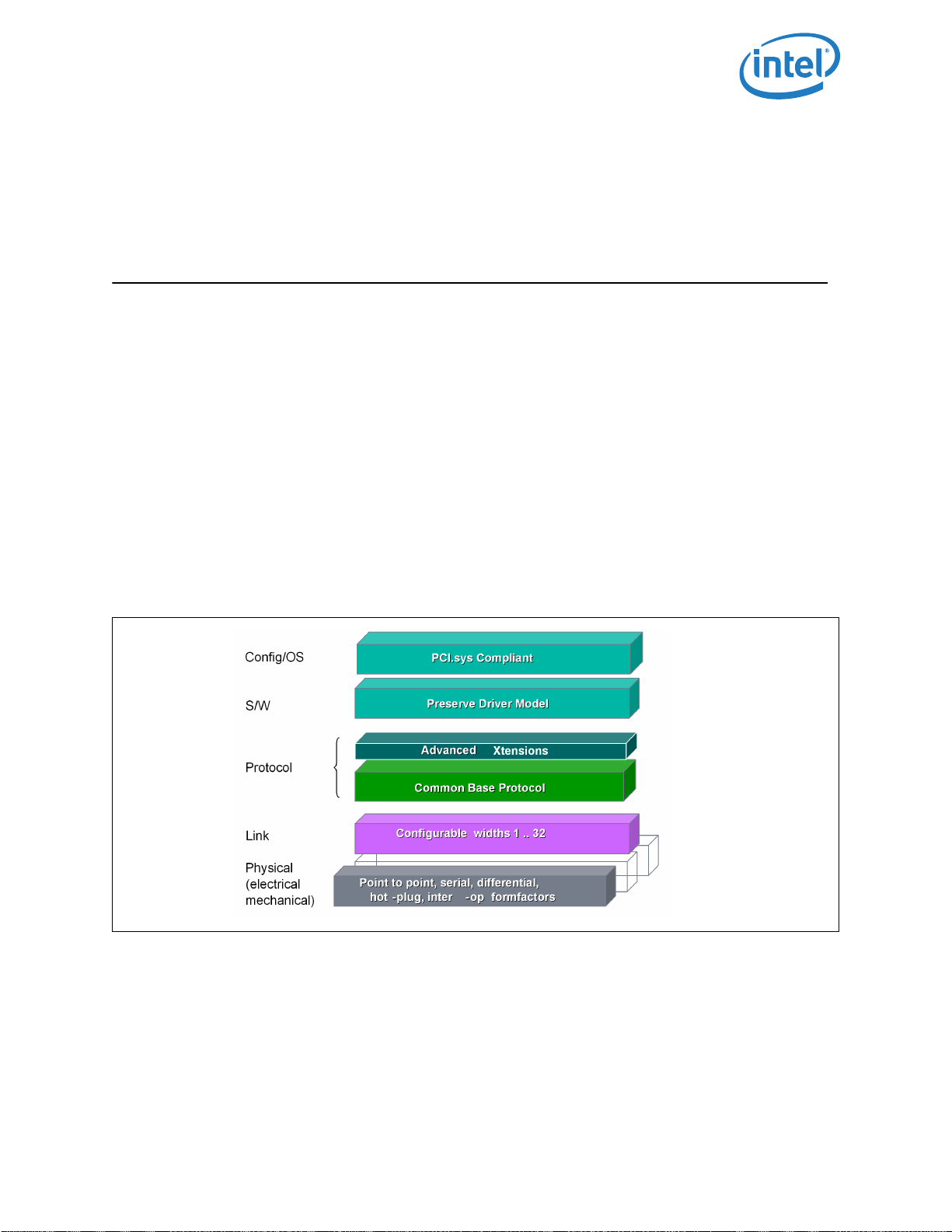
Interconnects — Intel® 82576EB GbE Controller
3.0 Interconnects
3.1 PCIe
3.1.1 PCIe Overview
PCIe is a third generation I/O architecture that enables cost competitive next generation I/O solutions
providing industry leading price/performance and feature richness. It is an industry-driven
specification.
PCIe defines a basic set of requirements that encases the majority of the targeted application classes.
Higher-end applications' requirements, such as enterprise class servers and high-end communication
platforms, are encased by a set of advanced extensions that compliment the baseline requirements.
To guarantee headroom for future applications of PCIe, a software-managed mechanism for introducing
new, enhanced, capabilities in the platform is provided. Figure 3-1 shows PCIe architecture.
Figure 3-1. PCIe Stack Structure
PCIe's physical layer consists of a differential transmit pair and a differential receive pair. Full-duplex
data on these two point-to-point connections is self-clocked such that no dedicated clock signals are
required. The bandwidth of this interface increases linearly with frequency.
®
Revision: 2.63 Intel
December 2011 Datasheet
77
82576EB GbE Controller
Page 78

Intel® 82576EB GbE Controller — Interconnects
The packet is the fundamental unit of information exchange and the protocol includes a message space
to replace the various side-band signals found on many buses today. This movement of hard-wired
signals from the physical layer to messages within the transaction layer enables easy and linear
physical layer width expansion for increased bandwidth.
The common base protocol uses split transactions and several mechanisms are included to eliminate
wait states and to optimize the reordering of transactions to further improve system performance.
3.1.1.1 Architecture, Transaction and Link Layer Properties
• Split transaction, packet-based protocol
• Common flat address space for load/store access (such as PCI addressing model)
— Memory address space of 32-bit to allow compact packet header (must be used to access
addresses below 4 GB)
— Memory address space of 64-bit using extended packet header
• Transaction layer mechanisms:
— PCI-X style relaxed ordering
— Optimizations for no-snoop transactions
• Credit-based flow control
• Packet sizes/formats:
— Maximum packet size supports 128 byte and 256 byte data payload
— Maximum read request size of 512 bytes
• Reset/initialization:
— Frequency/width/profile negotiation performed by hardware
• Data integrity support
— Using CRC-32 for transaction layer packets
• Link layer retry for recovery following error detection
— Using CRC-16 for link layer messages
• No retry following error detection
— 8b/10b encoding with running disparity
• Software configuration mechanism:
— Uses PCI configuration and bus enumeration model
— PCIe-specific configuration registers mapped via PCI extended capability mechanism
• Baseline messaging:
— In-band messaging of formerly side-band legacy signals (such as interrupts, etc.)
— System-level power management supported via messages
• Power management:
— Full support for PCI-PM
— Wake capability from D3cold state
— Compliant with ACPI, PCI-PM software model
— Active state power management
Intel® 82576EB GbE Controller Revision: 2.63
Datasheet December 2011
78
Page 79

Interconnects — Intel® 82576EB GbE Controller
• Support for PCIe v2.0 (2.5GT/s)
— Support for completion time out
— Support for additional registers in the PCIe capability structure.
3.1.1.2 Physical Interface Properties
• Point to point interconnect
— Full-duplex; no arbitration
• Signaling technology:
— Low Voltage Differential (LVD)
— Embedded clock signaling using 8b/10b encoding scheme
• Serial frequency of operation: 2.5 GHz.
• Interface width of x4, x2, or x1.
• DFT and DFM support for high volume manufacturing
3.1.1.3 Advanced Extensions
PCIe defines a set of optional features to enhance platform capabilities for specific usage modes. The
82576 supports the following optional features:
• Advanced Error Reporting - messaging support to communicate multiple types/severity of errors
• Device serial number - Allows exposure of a unique serial number for each device.
• Alternative Requester ID (ARI) - allow support of more than 8 function per device.
• Single Root I/O virtualization (PCI-SIG SR-IOV) - allows exposure of virtual functions controlling a
subset of the resources to virtual machines.
3.1.2 Functionality - General
3.1.2.1 Native/Legacy
• All the 82576 PCI functions are native PCIe functions.
3.1.2.2 Locked Transactions
• The 82576 does not support locked requests as target or master.
3.1.2.3 End to End CRC (ECRC)
• Not supported by the 82576
®
Revision: 2.63 Intel
December 2011 Datasheet
79
82576EB GbE Controller
Page 80

Intel® 82576EB GbE Controller — Interconnects
3.1.3 Host I/F
3.1.3.1 Tag IDs
PCIe device numbers identify logical devices within the physical device (the 82576 is a physical device).
The 82576 implements a single logical device with up to two separate PCI functions: LAN 0, and LAN 1.
The device number is captured from each type 0 configuration write transaction.
Each of the PCIe functions interfaces with the PCIe unit through one or more clients. A client ID
identifies the client and is included in the Tag field of the PCIe packet header. Completions always carry
the tag value included in the request to enable routing of the completion to the appropriate client.
Tag IDs are allocated differently for read and write. Messages are sent with a tag of 0x1F.
3.1.3.1.1 TAG ID Allocation for Read Transactions
Table 3-1 lists the Tag ID allocation for read accesses. The tag ID is interpreted by hardware in order to
forward the read data to the required device.
Table 3-1. IDs in Read Transactions
Tag ID Description Comment
0 Reserved
1 Descriptor Rx Like 82571/82572/82575
2 Reserved
3 Reserved
4 Descriptor Tx Like 82571/82572/82575
5 Reserved
6 Reserved
7 Reserved
8 Data request 0 Like 82571/82572/82575
9 Data request 1 Like 82571/82572/82575
0a Data request 2 Like 82571/82572/82575
0b Data request 3 Like 82571/82572/82575
10 Reserved
11 Message unit
12-1F Reserved
3.1.3.1.2 TAG ID Allocation for Write Transactions
Request tag allocation depends on these system parameters:
• DCA supported/not supported in the system (DCA_CTRL.DCA_DIS - see Section 8.13.4 for details)
• DCA enabled/disabled for each type of traffic (TXCTL.TX Descriptor DCA EN, RXCTL.RX Descriptor
DCA EN, RXCTL.RX Header DCA EN, RXCTL.Rx Payload DCA EN)
Intel® 82576EB GbE Controller Revision: 2.63
Datasheet December 2011
80
Page 81

Interconnects — Intel® 82576EB GbE Controller
• System type: Legacy DCA vs. DCA 1.0 (DCA_CTRL.DCA_MODE - see Section 8.13.4 for details).
• CPU ID (RXCTL.CPUID or TXCTL.CPUID)
Since DCA is implemented differently in I/OAT 1 and in I/OAT 2/3 platforms, the tag IDs are different as
well (see Section 3.1.3.1.2.3 below).
3.1.3.1.2.1 Case 1 - DCA Disabled in the System:
Table 3-2 describes the write requests tags. Unlike read, the values are for debug only, allowing tracing
of requests through the system.
Table 3-2. IDs in Write Transactions, DCA Disabled Mode
Tag ID Description
0x0 - 0x1 Reserved
0x2 Tx descriptors write-back / Tx Head write-back
0x3 Reserved
0x4 Rx descriptors write-back
0x5 Reserved
0x6 Write data
0x7 - 0x1D Reserved
0x1E MSI and MSI-X
0x1F Reserved
3.1.3.1.2.2 Case 2 - DCA Enabled in the System, but Disabled for the Request:
• Legacy DCA platforms - If DCA is disabled for the request, the tags allocation is identical to the case
where DCA is disabled in the system. See Table 3-2 above.
• DCA 1.0 platforms - All write requests have the tag of 0x00.
Note: When in DCA 1.0 mode, messages and MSI/MSI-x write requests are sent with the no-hint
tag.
3.1.3.1.2.3 Case 3 - DCA Enabled in the System, DCA Enabled for the Request:
• Legacy DCA Platforms: the request tag is constructed as follows:
— Bit[0] – DCA Enable
— Bits[3:1] - The CPU ID field taken from the CPUID[2:0] bits of the RXCTL or TXCTL registers
— Bits[7:4] - Reserved
• DCA 1.0 Platforms: the request tag (all 8 bits) is taken from the CPUID field of the RXCTL or TXCTL
registers
3.1.3.2 Completion Timeout Mechanism
In any split transaction protocol, there is a risk associated with the failure of a requester to receive an
expected completion. To enable requesters to attempt recovery from this situation in a standard
manner, the completion timeout mechanism is defined.
®
Revision: 2.63 Intel
December 2011 Datasheet
81
82576EB GbE Controller
Page 82

Intel® 82576EB GbE Controller — Interconnects
The completion timeout mechanism is activated for each request that requires one or more completions
when the request is transmitted. The PCIe specification, Rev. 1.1 requires that the completion timeout
timer:
• Should not expire in less than 10 ms.
• Must expire if a request is not completed within 50 ms.
However, some platforms experience completion latencies that are longer than 50 ms, in some cases up
to seconds. In PCIe specification, Rev 2.0 an mechanism to allow configuration of the completion
timeout was added. The 82576 supports both the legacy Rev. 1.1 and the default Rev 2.0 mechanisms,
To support the legacy mode, it provides a programmable range for the completion timeout, as well as
the ability to disable completion timeout altogether. The default PCIe Rev 2.0 mode programs
completion timeout through an extension of the PCIe capability structure. The new capability structure
is assigned a PCIe capability structure version of 0x2.
The 82576 controls the following aspects of completion timeout:
• Disabling or enabling completion timeout
• Disabling or enabling resending a request on completion timeout
• A programmable range of timeout values
Programming the behavior of the completion timeout is done differently whether capability Structure
version 0x1 is enabled or capability structure version 0x2 is enabled. Table 3-3 lists the behavior for
both cases.
Table 3-3. Completion Timeout Programming
Capability Capability Structure Version = 0x1 Capability Structure Version = 0x2
Completion timeout enabling
Resend request enable
Completion timeout period Loaded from EEPROM into CSR bit.
Loaded from EEPROM into
Completion_Timeout_Disable bit in the
PCIe Control Register (GCR 0x05000).
Loaded from EEPROM into
Completion_Timeout_Resend bit in the
PCIe Control Register (GCR, 0x05000).
Controlled through PCIe configuration
space Device Control 2 Register (0xC8)
bit 4. Visible through read-only CSR
Same as version = 0x1
Controlled through PCIe configuration
space Device Control 2 Register (0xC8)
bits 3:0.
Visible through read-only CSR bit.
The capability structure exposed and the mode used are fixed by the GIO_CAP field in the PCIe Init
Configuration 3 EEPROM Word (Word 0x1A).
3.1.3.2.1 Completion Timeout Enable
• Version = 0x1- Loaded from the Completion Timeout Disable bit in the EEPROM (Word 0x15, bit 7)
into the Completion_Timeout_Disable bit in the PCIe Control Register (GCR). Completion Timeout
enabled is the default.
• Version = 0x2 - Programmed through PCIe configuration space Device Control 2 Register (0xC8) bit
4.. Visible through the Completion_Timeout_Disable bit in the PCIe Control Register (GCR).
Completion Timeout enabled is the default.
3.1.3.2.2 Resend Request Enable
Intel® 82576EB GbE Controller Revision: 2.63
Datasheet December 2011
82
Page 83

Interconnects — Intel® 82576EB GbE Controller
• Version = 0x1- The Completion Timeout Resend EEPROM bit (Word 0x15, bit 4) , loaded to the
Completion_Timeout_Resend bit in the PCIe Control Register (GCR), enables resending the request
(applies only when completion timeout is enabled). The default is to resend a request that timed
out.
• Version = 0x2 - same as when version = 0x1.
3.1.3.2.3 Completion Timeout Period
• Version = 0x1.- Loaded from the Completion Timeout Value field in the EEPROM (word 0x15, bits
6:5) to the Completion_Timeout_Value bits in the PCIe Control Register (GCR). The following
values are supported.
Setting: Completion Timeout Value PCIe Spec defined ranges Ranges implemented
00 (default) 50 μs to 10 ms 500 μs – 1 ms
01 10 ms to 250 ms 50 ms – 100 ms
10 250 ms to 4 s 500 ms – 1s
11 4 s to 64 s 10s – 20s
• Version = 0x2 - Programmed through PCI configuration. Visible through the
Completion_Timeout_Value bits in the PCIe Control Register (GCR). The 82576 supports all four
ranges defined by the PCIe ECR.
— 50 us to 10 ms
— 10 ms to 250 ms
— 250 ms to 4 s
— 4 s to 64 s
System software programs a range (one of nine possible ranges that sub-divide the four ranges
previously mentioned) into the PCIe configuration space Device Control 2 Register (0xC8) bits 3:0. The
following are supported sub-ranges.
Setting: Completion Timeout
Value Device Control 2 Register
(0xC8) bits 3:0
0000 (default) 50 μs- 10 ms 500 μs – 1ms
0001 50 us – 100 μs 50 μs – 100 us
0010 1 ms- 10 ms 2 ms – 4 ms
0101 16 ms – 55 ms 16 ms – 32 ms
0110 65 ms – 210 ms 65 ms – 130 ms
1001 260 ms – 900 ms 260 ms – 520 ms
1010 1 s – 3.5 s 1 s – 2 s
1101 4 s – 13 s 4 s – 8 s
1110 17 s – 64 s 17 s – 34 s
Revision: 2.63 Intel
December 2011 Datasheet
83
PCIe defined ranges Ranges implemented
®
82576EB GbE Controller
Page 84

Intel® 82576EB GbE Controller — Interconnects
A memory read request for which there are multiple completions is considered completed only when all
completions are received by the requester. If some, but not all, requested data is returned before the
completion timeout timer expires, the requestor is permitted to keep or to discard the data that was
returned prior to timer expiration.
Note: The completion timeout value must be programmed correctly in PCIe configuration space in
(Device Control 2 Register); the value must be set above the expected maximum latency
for completions in the system in which the device is installed. This will ensure that the
device receives the completions for the requests it sends out, avoiding a completion timeout
scenario. It is expected that the system BIOS will set this value appropriately for the
system.
3.1.4 Transaction Layer
The upper layer of the PCIe architecture is the transaction Layer. The transaction layer connects to the
82576 core using an implementation specific protocol. Through this core-to-transaction-layer protocol,
the application-specific parts of the 82576 interact with the PCIe subsystem and transmit and receive
requests to or from the remote PCIe agent, respectively.
3.1.4.1 Transaction Types Accepted by the 82576
Table 3-4. Transaction Types at the Rx Transaction Layer
Transaction Type FC Type
Configuration Read
Request
Configuration Write
Request
Memory Read Request NPH CPLH + CPLD Requester ID, TAG, Attribute CSR
Memory Write Request PH +
IO Read Request NPH CPLH + CPLD Requester ID, TAG, Attribute CSR
IO Write Request NPH + NPD CPLH Requester ID, TAG, Attribute CSR
Read completions CPLH +
Message PH - - Message Unit / INT / PM /
NPH CPLH + CPLD Requester ID, TAG, Attribute Configuration space
NPH + NPD CPLH Requester ID, TAG, Attribute Configuration space
PD
CPLD
Tx Later
Reaction
- - CSR
- - DMA
Hardware Should Keep Data
From Original Packet
For Client
Error Unit
Flow control types:
• PH - Posted request headers
• PD - Posted request data payload
• NPH - Non-posted request headers
• NPD - Non-posted request data payload
• CPLH - Completion headers
• CPLD - Completion data payload
Intel® 82576EB GbE Controller Revision: 2.63
Datasheet December 2011
84
Page 85

Interconnects — Intel® 82576EB GbE Controller
3.1.4.1.1 Configuration Request Retry Status
PCIe supports devices requiring a lengthy self-initialization sequence to complete before they are able
to service configuration requests as it is the case for the 82576 that might have a delay in initialization
due to an EEPROM read.
If the read of the PCIe section in the EEPROM was not completed and the 82576 receives a
configuration request, the 82576 responds with a configuration request retry completion status to
terminate the request, and thus effectively stall the configuration request until such time that the
subsystem has completed local initialization and is ready to communicate with the host.
3.1.4.1.2 Partial Memory Read and Write Requests
The 82576 has limited support of read and write requests when only part of the byte enable bits are set
as described later in this section.
Partial writes to the MSI-X table are supported. All other partial writes are ignored and a completion
abort is sent.
Zero-length writes have no internal impact (nothing written, no effect such as clear-by-write). The
transaction is treated as a successful operation (no error event).
Partial reads with at least one byte enabled are answered as a full read. Any side effect of the full read
(such as clear by read) is applicable to partial reads also.
Zero-length reads generate a completion, but the register is not accessed and undefined data is
returned.
3.1.4.2 Transaction Types Initiated by the 82576
Table 3-5. Transaction Types at the Tx Transaction Layer
Transaction type Payload Size FC Type From Client
Configuration Read Request Completion Dword CPLH + CPLD Configuration space
Configuration Write Request Completion - CPLH Configuration space
I/O Read Request Completion Dword CPLH + CPLD CSR
I/O Write Request Completion - CPLH CSR
Read Request Completion Dword/Qword CPLH + CPLD CSR
Memory Read Request - NPH DMA
Memory Write Request <= MAX_PAYLOAD_SIZE PH + PD DMA
Message - PH Message Unit / INT /
Note: MAX_PAYLOAD_SIZE supported is loaded from EEPROM (128 bytes, 256 bytes or 512 bytes). IF ARI capability is not
exposed, the effective MAX_PAYLOAD_SIZE is defined for each PCI functions according to configuration space register of
this function. If ARI capability is exposed, effective MAX_PAYLOAD_SIZE is defined for all PCI functions according to
configuration space register of function zero
PM / Error Unit
3.1.4.2.1 Data Alignment
®
Revision: 2.63 Intel
December 2011 Datasheet
85
82576EB GbE Controller
Page 86

Intel® 82576EB GbE Controller — Interconnects
Requests must never specify an address/length combination that causes a memory space access to
cross a 4 KB boundary. The 82576 breaks requests into 4 KB-aligned requests (if needed). This does
not pose any requirement on software. However, if software allocates a buffer across a 4 KB boundary,
hardware issues multiple requests for the buffer. Software should consider limiting buffer sizes and
base addresses to comply with a 4 KB boundary in cases where it improves performance.
The general rules for packet alignment are as follows:
1. The length of a single request should not exceed the PCIe limit of MAX_PAYLOAD_SIZE for write
and MAX_READ_REQ for read.
2. The length of a single request does not exceed the 82576’s internal limitations 512 bytes.
3. A single request should not span across different memory pages as noted by the 4 KB boundary
previously mentioned.
Note: The rules apply to all the 82576 requests (read/write, snoop and no snoop).
If a request can be sent as a single PCIe packet and still meet rules 1-3, then it is not broken at a
cache-line boundary (as defined in the PCIe Cache line size configuration word), but rather, sent as a
single packet (motivation is that the chipset might break the request along cache-line boundaries, but
the 82576 should still benefit from better PCIe utilization). However, if rules 1-3 require that the
request is broken into two or more packets, then the request is broken at a cache-line boundary.
3.1.4.2.2 Multiple Tx Data Read Requests
The 82576 supports four pipe lined requests for transmit data. In general, the four requests might
belong to the same packet or to consecutive packets. However, the following restriction applies:
• All requests for a packet are issued before a request is issued for a consecutive packet
Read requests can be issued from any of the supported queues, as long as the restriction is met.
Pipelined requests might belong to the same queue or to separate queues. However, as previously
noted, all requests for a certain packet are issued (from same queue) before a request is issued for a
different packet (potentially from a different queue).
The PCIe specification does not insure that completions for separate requests return in-order. Read
completions for concurrent requests are not required to return in the order issued. The 82576 handles
completions that arrive in any order. Once all completions arrive for a given request, the 82576 might
issue the next pending read data request.
• The 82576 incorporates a 2 KB re-order buffer to support re-ordering of completions for four
requests. Each request/completion can be up to 512 bytes long. The maximum size of a read
request is defined as the minimum {512, Max_Read_Request_Size}.
In addition to the four pipeline requests for transmit data, the 82576 can issue a single read request for
each of the Tx descriptors and Rx descriptors. The requests for Tx data, Tx descriptor, and Rx descriptor
are independently issued. Each descriptor read request can fetch up to 16 descriptors (equal to 256
bytes of data).
3.1.4.3 Messages
3.1.4.3.1 Message Handling by the 82576 (as a Receiver)
Message packets are special packets that carry a message code.
The upstream device transmits special messages to the 82576 by using this mechanism.
Intel® 82576EB GbE Controller Revision: 2.63
Datasheet December 2011
86
Page 87

Interconnects — Intel® 82576EB GbE Controller
The transaction layer decodes the message code and responds to the message accordingly.
Table 3-6. Supported Message in the 82576 (as a Receiver)
Message
code [7:0]
0x14 100 PM_Active_State_NAK Internal signal set
0x19 011 PME_Turn_Off Internal signal set
0x50 100 Slot power limit support (has one Dword data) Silently drop
0x7E 010,011,100 Vendor_defined type 0 no data Unsupported request
0x7E 010,011,100 Vendor_defined type 0 data Unsupported request
0x7F 010,011,100 Vendor_defined type 1 no data Silently drop
0x7F 010,011,100 Vendor_defined type 1 data Silently drop
0x00 011 Unlock Silently drop
1. No Completion is expected for this type of packets
Routing r2r1r0 Message Device later response
3.1.4.3.2 Message Handling by the 82576 (as a Transmitter)
1
1
The transaction layer is also responsible for transmitting specific messages to report internal/external
events (such as interrupts and PMEs).
Table 3-7. Supported Message in the 82576 (as a Transmitter)
Message code
[7:0]
0x20 100 Assert INT A
0x21 100 Assert INT B
0x22 100 Assert INT C
0x23 100 Assert INT D
0x24 100 De-assert INT A
0x25 100 De-assert INT B
0x26 100 De-assert INT C
0x27 100 De-Assert INT D
0x30 000 ERR_COR
0x31 000 ERR_NONFATAL
0x33 000 ERR_FATAL
0x18 000 PM_PME
0x1B 101 PME_TO_ACK
Routing r2r1r0 Message
3.1.4.4 Ordering Rules
The 82576 meets the PCIe ordering rules (PCI-X rules) by following the PCI simple device model:
®
Revision: 2.63 Intel
December 2011 Datasheet
87
82576EB GbE Controller
Page 88

Intel® 82576EB GbE Controller — Interconnects
• Deadlock avoidance - Master and target accesses are independent - The response to a target
access does not depend on the status of a master request to the bus. If master requests are
blocked, such as due to no credits, target completions might still proceed (if credits are available).
• Descriptor/data ordering - The 82576 does not proceed with some internal actions until respective
data writes have ended on the PCIe link:
— The 82576 does not update an internal header pointer until the descriptors that the header
pointer relates to are written to the PCIe link.
— The 82576 does not issue a descriptor write until the data that the descriptor relates to is
written to the PCIe link.
The 82576 might issue the following master read request from each of the following clients:
• Rx Descriptor Read (one for each LAN port)
• Tx Descriptor Read (two for each LAN port)
• Tx Data Read (up to four for each LAN port/ one for the manageability)
Completion separate read requests are not guaranteed to return in order. Completions for a single read
request are guaranteed to return in address order.
3.1.4.4.1 Out of Order Completion Handling
In a split transaction protocol, when using multiple read requests in a multi processor environment,
there is a risk that completions arrive from the host memory out of order and interleaved. In this case,
the 82576 sorts the request completion and transfers them to the Ethernet in the correct order.
3.1.4.5 Transaction Definition and Attributes
3.1.4.5.1 Max Payload Size
The 82576 policy to determine Max Payload Size (MPS) is as follows:
• Master requests initiated by the 82576 (including completions) limits MPS to the value defined for
the function issuing the request.
• Target write accesses to the 82576 are accepted only with a size of one Dword or two Dwords.
Write accesses in the range of (three Dwords, MPS, etc.) are flagged as UR. Write accesses above
MPS are flagged as malformed.
3.1.4.5.2 Traffic Class (TC) and Virtual Channels (VC)
The 82576 only supports TC=0 and VC=0 (default).
3.1.4.5.3 Relaxed Ordering
The 82576 takes advantage of the relaxed ordering rules in PCIe. By setting the relaxed ordering bit in
the packet header, the 82576 enables the system to optimize performance in the following cases:
• Relaxed ordering for descriptor and data reads: When the 82576 emits a read transaction, its split
completion has no ordering relationship with the writes from the CPUs (same direction). It should
be allowed to bypass the writes from the CPUs.
• Relaxed ordering for receiving data writes: When the 82576 masters receive data writes, it also
enables them to bypass each other in the path to system memory because software does not
process this data until their associated descriptor writes complete.
Intel® 82576EB GbE Controller Revision: 2.63
Datasheet December 2011
88
Page 89

Interconnects — Intel® 82576EB GbE Controller
• The 82576 cannot relax ordering for descriptor writes, MSI/MSI-X writes or PCIe messages.
Relaxed ordering can be used in conjunction with the no-snoop attribute to enable the memory
controller to advance non-snoop writes ahead of earlier snooped writes.
Relaxed ordering is enabled in the 82576 by clearing the RO_DIS bit in the CTRL_EXT register. Actual
setting of relaxed ordering is done for LAN traffic by the host through the DCA registers.
3.1.4.5.4 Snoop Not Required
The 82576 sets the Snoop Not Required attribute bit for master data writes. System logic might provide
a separate path into system memory for non-coherent traffic. The non-coherent path to system
memory provides higher, more uniform, bandwidth for write requests.
Note: The Snoop Not Required attribute does not alter transaction ordering. Therefore, to achieve
maximum benefit from Snoop Not Required transactions, it is advisable to set the relaxed
ordering attribute as well (assuming that system logic supports both attributes). In fact,
some chipsets require that relaxed ordering is set for no-snoop to take effect.
Global no-snoop support is enabled in the 82576 by clearing the NS_DIS bit in the CTRL_EXT register.
Actual setting of no snoop is done for LAN traffic by the host through the DCA registers.
3.1.4.5.5 No Snoop and Relaxed Ordering for LAN Traffic
Software might configure non-snoop and relax order attributes for each queue and each type of
transaction by setting the respective bits in the RXCTRL and TXCTRL registers.
Table 3-8 lists the default behavior for the No-Snoop and Relaxed Ordering bits for LAN traffic when I/
OAT 2 is enabled.
Table 3-8. LAN Traffic Attributes
Transaction No-Snoop Default
Rx Descriptor Read N Y
Rx Descriptor Write-Back N N Relaxed ordering must never be
Rx Data Write Y Y See the following note and
Rx Replicated Header N Y
Tx Descriptor Read N Y
Tx Descriptor Write-Back N Y
Tx TSO Header Read N Y
Tx Data Read N Y
Note: Rx payload no-snoop is also conditioned by the NSE bit in the receive descriptor. See
Section 3.1.4.5.5.1.
Relaxed Ordering
Default
Comments
used for this traffic.
Section 3.1.4.5.5.1
®
Revision: 2.63 Intel
December 2011 Datasheet
89
82576EB GbE Controller
Page 90

Intel® 82576EB GbE Controller — Interconnects
3.1.4.5.5.1 No-Snoop Option for Payload
Under certain conditions, which occur when I/OAT is enabled, software knows that it is safe to transfer
(DMA) a new packet into a certain buffer without snooping on the front-side bus. This scenario typically
occurs when software is posting a receive buffer to hardware that the CPU has not accessed since the
last time it was owned by hardware. This might happen if the data was transferred to an application
buffer by the I/OAT DMA engine.
In this case, software should be able to set a bit in the receive descriptor indicating that the 82576
should perform a no-snoop DMA transfer when it eventually writes a packet to this buffer.
When a non-snoop transaction is activated, the TLP header has a non-snoop attribute in the
Transaction Descriptor field.
This is triggered by the NSE bit in the receive descriptor. See Section 7.1.5.
3.1.4.5.5.2 No Snoop Option for TSO Header
As hardware reads the header of a TSO request for each segment it sends, we may safely assume that
after the first read of the header it is updated in the main memory. As as result, all the subsequent
reads of the header might be done with the no-snoop option set. This option is triggered by setting the
NoSnoop_LSO_hdr_buf bit in the DTXCTL register.
3.1.4.6 Flow Control
3.1.4.6.1 82576 Flow Control Rules
The 82576 implements only the default Virtual Channel (VC0). A single set of credits is maintained for
VC0.
Table 3-9. Allocation of FC Credits
Credit Type Operations Number Of Credits
Posted Request Header (PH) Target Write (one unit)
Message (one unit)
Posted Request Data (PD) Target Write (Length/16 bytes=1)
Message (one unit)
Non-Posted Request Header (NPH) Target Read (one unit)
Configuration Read (one unit)
Configuration Write (one unit)
Non-Posted Request Data (NPD) Configuration Write (one unit) Two units.
Completion Header (CPLH) Read Completion (N/A) Infinite (accepted immediately).
Completion Data (CPLD) Read Completion (N/A) Infinite (accepted immediately).
Rules for FC updates:
Two units (to enable concurrent
accesses to both LAN ports).
MAX_PAYLOAD_SIZE/16
Two units (to enable concurrent target
accesses to both LAN ports).
• The 82576 maintains two credits for NPD at any given time. It increments the credit by one after
the credit is consumed and sends an UpdateFC packet as soon as possible. UpdateFC packets are
scheduled immediately after a resource is available.
Intel® 82576EB GbE Controller Revision: 2.63
Datasheet December 2011
90
Page 91

Interconnects — Intel® 82576EB GbE Controller
• The 82576 provides two credits for PH (such as for two concurrent target writes) and two credits for
NPH (such as for two concurrent target reads). UpdateFC packets are scheduled immediately after
a resource becomes available.
• The 82576 follows the PCIe recommendations for frequency of UpdateFC FCPs.
3.1.4.6.2 Upstream Flow Control Tracking
The 82576 issues a master transaction only when the required FC credits are available. Credits are
tracked for posted, non-posted, and completions (the later to operate against a switch).
3.1.4.6.3 Flow Control Update Frequency
In any case, UpdateFC packets are scheduled immediately after a resource becomes available.
When the link is in the L0 or L0s link state, Update FCPs for each enabled type of non-infinite FC credit
must be scheduled for transmission at least once every 30 μs (-0%/+50%), except when the Extended
Sync bit of the Control Link register is set, in which case the limit is 120 μs (-0%/+50%).
3.1.4.6.4 Flow Control Timeout Mechanism
The 82576 implements the optional FC update timeout mechanism.
The mechanism is activated when the Link is in L0 or L0s Link state. It uses a timer with a limit of
200μs (-0%/+50%), where the timer is reset by the receipt of any Init or Update FCP. Alternately, the
timer may be reset by the receipt of any DLLP.
After timer expiration, the mechanism instructs the PHY to re-establish the link (via the LTSSM recovery
state).
3.1.4.7 Error Forwarding
If a TLP is received with an error-forwarding trailer, the packet is dropped and not delivered to its
destination. The 82576 does not initiate any additional master requests for that PCI function until it
detects an internal reset or a software reset for the associated LAN. Software is able to access device
registers after such a fault.
System logic is expected to trigger a system-level interrupt to inform the operating system of the
problem. The operating system can then stop the process associated with the transaction, re-allocate
memory instead of the faulty area, etc.
3.1.5 Data Link Layer
3.1.5.1 ACK/NAK Scheme
The 82576 supports two alternative schemes for ACK/NAK rate:
1. ACK/NAK is scheduled for transmission according to timeouts specified in the LTIV register
2. ACK/NAK is scheduled for transmission according to timeouts specified in the PCIe specification.
The PCIe Error Recovery bit loaded from EEPROM determines which of the two schemes is used.
®
Revision: 2.63 Intel
December 2011 Datasheet
91
82576EB GbE Controller
Page 92

3.1.5.2 Supported DLLPs
The following DLLPs are supported by the 82576 as a receiver:
Table 3-10. DLLPs Received by the 82576
DLLP type Remarks
Ack
Nak
PM_Request_Ack
InitFC1-P Virtual Channel 0 only
InitFC1-NP Virtual Channel 0 only
InitFC1-Cpl Virtual Channel 0 only
InitFC2-P Virtual Channel 0 only
InitFC2-NP Virtual Channel 0 only
InitFC2-Cpl Virtual Channel 0 only
UpdateFC-P Virtual Channel 0 only
UpdateFC-NP Virtual Channel 0 only
Intel® 82576EB GbE Controller — Interconnects
UpdateFC-Cpl Virtual Channel 0 only
The following DLLPs are supported by the 82576 as a transmitter:
Table 3-11. DLLPs Initiated by the 82576
DLLP type Remarks
Ack
Nak
PM_Enter_L1
PM_Enter_L23
PM_Active_State_Request_L1
InitFC1-P Virtual Channel 0 only
InitFC1-NP Virtual Channel 0 only
InitFC1-Cpl Virtual Channel 0 only
InitFC2-P Virtual Channel 0 only
InitFC2-NP Virtual Channel 0 only
InitFC2-Cpl Virtual Channel 0 only
UpdateFC-P Virtual Channel 0 only
UpdateFC-NP Virtual Channel 0 only
Note: UpdateFC-Cpl is not sent because of the infinite FC-Cpl allocation.
Intel® 82576EB GbE Controller Revision: 2.63
Datasheet December 2011
92
Page 93

Interconnects — Intel® 82576EB GbE Controller
3.1.5.3 Transmit EDB Nullifying
In case of a retrain necessity, there is a need to guarantee that no abrupt termination of the Tx packet
happens. For this reason, early termination of the transmitted packet is possible. This is done by
appending an EDB (EnD Bad symbol) to the packet.
3.1.6 Physical Layer
3.1.6.1 Link Width
The 82576 supports a maximum link width of x4, x2, or x1 as determined by the Lane_Width field in
PCIe Init Configuration 3 EEPROM word.
The max link width is loaded into the Maximum Link Width field of the PCIe Capability register
(LCAP[11:6]). The hardware default is x4 link.
During link configuration, the platform and the 82576 negotiate on a common link width. The link width
must be one of the supported PCIe link widths (x1, x2, x4), such that:
• If Maximum Link Width = x4, then the 82576 negotiates to either x4, x2 or x1.
• If Maximum Link Width = x2, then the 82576 negotiates to either x2 or x1.
• If Maximum Link Width = x1, then the 82576 only negotiates to x1.
1
3.1.6.2 Polarity Inversion
If polarity inversion is detected, the receiver must invert the received data.
During the training sequence, the receiver looks at Symbols 6-15 of TS1 and TS2 as the indicator of
lane polarity inversion (D+ and D- are swapped). If lane polarity inversion occurs, the TS1 Symbols 615 received are D21.5 as opposed to the expected D10.2. Similarly, if lane polarity inversion occurs,
Symbols 6-15 of the TS2 ordered set are D26.5 as opposed to the expected D5.2. This provides the
clear indication of lane polarity inversion.
3.1.6.3 L0s Exit latency
The number of FTS sequences (N_FTS) sent during L1 exit, is loaded from the EEPROM into an 8-bit
read-only register.
3.1.6.4 Lane-to-Lane De-Skew
A multi-lane link might have many sources of lane-to-lane skew. Although symbols are transmitted
simultaneously on all lanes, they cannot be expected to arrive at the receiver without lane-to-lane
skew. The skew can include components, which are less than a bit time, bit time units (400 ps for 2.5
Gb), or full symbol time units (4 ns) of skew caused by the re-timing repeaters' insert/delete
operations. Receivers use TS1 or TS2 or Skip Ordered Sets (SOS) to perform link de-skew functions.
The 82576 supports de-skew of up to 6 symbols time (24 ns).
1. See restriction in Section 3.1.6.5.
®
Revision: 2.63 Intel
December 2011 Datasheet
93
82576EB GbE Controller
Page 94

Intel® 82576EB GbE Controller — Interconnects
3.1.6.5 Lane Reversal
The following lane reversal modes are supported (see Figure 3-2):
• Lane configuration of x4, x2, and x1
• Lane reversal in x4 and in x2
• Degraded mode (downshift) from x4 to x2 to x1 and from x2 to x1, with one restriction - if lane
reversal is executed in x4, then downshift is only to x1 and not to x2.
Note: The restriction requires that a x2 interface to the 82576 must connect to lanes 0 and 1 on
the 82576. The PCIe Card Electromechanical specification does not allow to route a x2 link
to a wider connector. Therefore, a system designer is not allowed to connect a x2 link to
lanes 2 and 3 of a PCIe connector. It is also recommended that when used in x2 mode on a
NIC, the 82576 is connected to lanes 0 and 1 of the NIC.
Figure 3-2. Lane Reversal Supported Modes
Configuration bits:
• EEPROM Lane Reversal Disable bit - disables lane reversal altogether. See Section 6.2.18, PCIe
Control (Word 0x1B) for the bit.
3.1.6.6 Reset
The PCIe PHY can supply core reset to the 82576. The reset can be caused by two sources:
1. Upstream move to hot reset - Inband Mechanism (LTSSM).
2. Recovery failure (LTSSM returns to detect).
3. Upstream component moves to Disable.
Intel® 82576EB GbE Controller Revision: 2.63
Datasheet December 2011
94
Page 95

Interconnects — Intel® 82576EB GbE Controller
3.1.6.7 Scrambler Disable
The scrambler/de-scrambler functionality in the 82576 can be eliminated by two mechanisms:
1. Upstream according to the PCIe specification.
2. EPROM bit.
3.1.7 Error Events and Error Reporting
3.1.7.1 Mechanism in General
PCIe defines two error reporting paradigms: the baseline capability and the Advanced Error Reporting
(AER) capability. The baseline error reporting capabilities are required of all PCIe devices and define the
minimum error reporting requirements. The AER capability is defined for more robust error reporting
and is implemented with a specific PCIe capability structure.
Both mechanisms are supported by the 82576.
Also the SERR# Enable and the Parity Error bits from the legacy Command register take part in the
error reporting and logging mechanism.
Figure 3-3 shows, in detail, the flow of error reporting in the 82576.
®
Revision: 2.63 Intel
December 2011 Datasheet
95
82576EB GbE Controller
Page 96

Intel® 82576EB GbE Controller — Interconnects
Figure 3-3. Error Reporting Mechanism
3.1.7.2 Error Events
Table 3-12 lists the error events identified by the 82576 and the response in terms of logging,
reporting, and actions taken. Consult the PCIe specification for the effect on the PCI Status register.
Table 3-12. Response and Reporting of Error Events
Error Name Error Events Default Severity Action
PHY errors
Receiver error 8b/10b decode errors
Packet framing error
Data link errors
Bad TLP • Bad CRC
• Not legal EDB
• Wrong sequence number
Intel® 82576EB GbE Controller Revision: 2.63
Datasheet December 2011
96
Correctable.
Send ERR_CORR
Correctable.
Send ERR_CORR
TLP to initiate NAK and drop data.
DLLP to drop.
TLP to initiate NAK and drop data.
Page 97

Interconnects — Intel® 82576EB GbE Controller
Table 3-12. Response and Reporting of Error Events (Continued)
Bad DLLP
• Bad CRC
Correctable.
Send ERR_CORR
DLLP to drop.
Replay timer
timeout
REPLAY NUM
rollover
Data link layer
protocol error
TLP errors
Poisoned TLP
received • TLP with error forwarding
Unsupported
Request (UR)
Completion
timeout
• REPLAY_TIMER expiration
• REPLAY NUM rollover
• Received ACK/NACK not
corresponding to any TLP
• Wrong configuration access
• MRdLk
• Configuration request type 1
• Unsupported vendor Defined
type 0 message
• Not valid MSG code
• Not supported TLP type
• Wrong function number
• Wrong TC/VC
• Received target access with
data size > 64-bit
• Received TLP outside address
range
• Completion timeout timer
expired
Correctable.
Send ERR_CORR
Correctable.
Send ERR_CORR
Uncorrectable.
Send ERR_FATAL
Uncorrectable.
ERR_NONFATAL
Log header
Uncorrectable.
ERR_NONFATAL
Log header
Uncorrectable.
ERR_NONFATAL
Follow LL rules.
Follow LL rules.
Follow LL rules.
A poisoned completion is ignored and
the request can be retried after
timeout. If enabled, the error is
reported.
Send completion with UR.
Send the read request again.
Completer abort
Unexpected
completion
Receiver overflow
Flow control
protocol error
Revision: 2.63 Intel
December 2011 Datasheet
97
• Attempts to write to the Flash
device when writes are
disabled (EEC.FWE=01b)
• Received completion without a
request for it (tag, ID, etc.)
• Received TLP beyond
allocated credits
• Minimum initial flow control
advertisements
• Flow control update for infinite
credit advertisement
Uncorrectable.
ERR_NONFATAL
Log header
Uncorrectable.
ERR_NONFATAL
Log header
Uncorrectable.
ERR_FATAL
Uncorrectable.
ERR_FATAL
Send completion with CA.
Discard TLP.
Receiver behavior is undefined.
Receiver behavior is undefined. The
82576 doesn’t report violations of
Flow Control initialization protocol
®
82576EB GbE Controller
Page 98

Intel® 82576EB GbE Controller — Interconnects
Table 3-12. Response and Reporting of Error Events (Continued)
Malformed TLP
(MP)
Completion with
unsuccessful
completion status
• Data payload exceed
Max_Payload_Size
• Received TLP data size does
not match length field
• TD field value does not
correspond with the observed
size
• Byte enables violations.
• Power management messages
that don’t use TC0.
• Usage of unsupported VC
Uncorrectable.
ERR_FATAL
Log header
No action (already
done by originator of
completion).
Drop the packet and free FC credits.
Free FC credits.
Byte count
integrity in
completion
process.
When byte count isn’t compatible
with the length field and the
actual expected completion
length. For example, length field
is 10 (in Dword), actual length is
40, but the byte count field that
indicates how many bytes are still
expected is smaller than 40,
which is not reasonable.
No action The 82576 doesn't check for this error
and accepts these packets.
This may cause a completion timeout
condition.
3.1.7.3 Error Pollution
Error pollution can occur if error conditions for a given transaction are not isolated to the error's first
occurrence. If the Physical layer detects and reports a receiver error, to avoid having this error
propagate and cause subsequent errors at upper layers the same packet is not signaled at the data link
or transaction layers.
Similarly, when the data link layer detects an error, subsequent errors that occur for the same packet
are not signaled at the transaction layer.
3.1.7.4 Completion with Unsuccessful Completion Status
A completion with unsuccessful completion status is dropped and not delivered to its destination. The
request that corresponds to the unsuccessful completion is retried by sending a new request for the
data that was not delivered.
3.1.7.5 Error Reporting Changes
The Rev. 1.1 specification defines two changes to advanced error reporting. A new Role-Based Error
Reporting bit in the Device Capabilities register is set to 1b to indicate that these changes are
supported by the 82576.
1. Setting the SERR# Enable bit in the PCI Command register also enables UR reporting (in the same
manner that the SERR# Enable bit enables reporting of correctable and uncorrectable errors). In
other words, the SERR# Enable bit overrides the UR Error Reporting Enable bit in the PCIe Device
Control register.
2. Changes in the response to some uncorrectable non-fatal errors, detected in non-posted requests
to the 82576. These are called advisory Non-fatal error cases. For each of the errors that follow, the
following behavior is defined:
Intel® 82576EB GbE Controller Revision: 2.63
Datasheet December 2011
98
Page 99

Interconnects — Intel® 82576EB GbE Controller
a. The Advisory Non-Fatal Error Status bit is set in the Correctable Error Status register to indicate
the occurrence of the advisory error and the Advisory Non-Fatal Error Mask corresponding bit in
the Correctable Error Mask register is checked to determine whether to proceed further with
logging and signaling.
b. If the Advisory Non-Fatal Error Mask bit is clear, logging proceeds by setting the corresponding
bit in the Uncorrectable Error Status register, based upon the specific uncorrectable error that's
being reported as an advisory error. If the corresponding uncorrectable error bit in the
Uncorrectable Error Mask register is clear, the First Error Pointer and Header Log registers are
updated to log the error, assuming they are not still occupied by a previously unserviced error.
c. An ERR_COR message is sent if the Correctable Error Reporting Enable bit is set in the Device
Control register. An ERROR_NONFATAL message is not sent for this error.
The following uncorrectable non-fatal errors are considered as advisory non-fatal Errors:
• A completion with an Unsupported Request or Completer Abort (UR/CA) status that signals an
uncorrectable error for a non-posted request. If the severity of the UR/CA error is non-fatal, the
completer must handle this case as an advisory non-fatal error.
• When the requester of a non-posted request times out while waiting for the associated completion,
the requester is permitted to attempt to recover from the error by issuing a separate subsequent
request, or to signal the error without attempting recovery. The requester is permitted to attempt
recovery zero, one, or multiple (finite) times, but must signal the error (if enabled) with an
uncorrectable error message if no further recovery attempt is made. If the severity of the
completion timeout is non-fatal and the requester elects to attempt recovery by issuing a new
request, the requester must first handle the current error case as an advisory non-fatal error.
• When a receiver receives an unexpected completion and the severity of the unexpected completion
error is non-fatal, the receiver must handle this case as an advisory non-fatal error.
3.1.8 Performance Monitoring
The 82576 incorporates PCIe performance monitoring counters to provide common capabilities to
evaluate performance. The 82576 implements four 32-bit counters to correlate between concurrent
measurements of events as well as the sample delay and interval timers. The four 32-bit counters can
also operate in a two 64-bit mode to count long intervals or payloads. software can reset, stop, or start
the counters (all at the same time).
The list of events supported by the 82576 and the counters control bits are described in the memory
register map (Section 8.6).
Some counters operate with a threshold - the counter increments only when the monitored event
crossed a configurable threshold (such as the number of available credits is below a threshold).
Counters operate in the following modes:
• Count mode - The counter increments when the respective event occurred.
• Leaky bucket mode - The counter increments only when the rate of events exceeded a certain
value. See Section 3.1.8.1.
3.1.8.1 Leaky Bucket Mode
Each of the counters may be configured independently to operate in a leaky bucket mode. When in
leaky bucket mode, the following functionality is provided:
• One of four 16-bit Leaky Bucket Counters (LBC) is enabled via the LBC Enable [3:0] bits in the PCIe
Statistic Control register #1.
®
Revision: 2.63 Intel
December 2011 Datasheet
99
82576EB GbE Controller
Page 100

Intel® 82576EB GbE Controller — Interconnects
• The LBC is controlled by the GIO_COUNT_START, GIO_COUNT_STOP, and GIO_COUNT_RESET bits
in the PCIe Statistic Control register #1.
• The LBC increments every time the respective event occurs.
• The LBC is decremented every T ms as defined in the LBC Timer field in the PCIe Statistic Control
registers.
• When an event occurs and the value of the LBC meets or exceeds the threshold defined in the LBC
Threshold field in the PCIe Statistic Control registers, the respective statistics counter increments.
3.1.9 PCIe Power Management
Described in Section 5.4.1 - Power Management.
3.1.10 PCIe Programming Interface
Described in Section 9.0 - PCIe Programming Interface
3.2 Management Interfaces
See Chapter 10.0, System Manageability.
The 82576 contains 2 possible interfaces to an external BMC.
• SMBus
•NC-SI
Since the manageability sideband throughput is lower than the network link throughput, the 82576
allocates an 8 KB internal buffer for incoming network packets prior to being sent over the sideband
interface.
3.2.1 SMBus
SMBus is an optional interface for pass-through and/or configuration traffic between an external MC
and the 82576. The SMBus commands used to configure or read status from the 82576 are described in
Chapter 10.0, System Manageability.
3.2.1.1 Channel Behavior
3.2.1.1.1 SMBus Addressing
The SMBus addresses that the 82576 responds to depend on the LAN mode (teaming/non-teaming).
When the LAN is in teaming mode (fail-over), the 82576 is presented over the SMBus as one device
along with one SMBus address. When in non-teaming mode in the LAN ports, the SMBus is presented
as two SMBus devices on the SMBus along with two SMBus addresses. In dual-address mode all passthrough functionality is duplicated on the SMBus address, where each SMBus address is connected to a
different LAN port.
Note: DO NOT configure both ports to the same address. When a LAN function is disabled, the
corresponding SMBus address is not presented to the external BMC.
Intel® 82576EB GbE Controller Revision: 2.63
Datasheet December 2011
100
 Loading...