

Page 1

Intel® Core™ i7 Processor with
Intel® QM57 Express Chipset
Development Kit User Guide
December 2009
Revision 001
323094
Page 2

INFORMATION IN THIS DOCUMENT IS PROVIDED IN CONNECTION WITH INTEL® PRODUCTS. NO LICENSE, EXPRESS OR
IMPLIED, BY ESTOPPEL OR OTHERWISE, TO ANY INTELLECTUAL PROPERTY RIGHTS IS GRANTED BY THIS DOCUMENT.
EXCEPT AS PROVIDED IN INTEL'S TERMS AND CONDITIONS OF SALE FOR SUCH PRODUCTS, INTEL ASSUMES NO
LIABILITY WHATSOEVER, AND INTEL DISCLAIMS ANY EXPRESS OR IMPLIED WARRANTY, RELATING TO SALE AND/OR
USE OF INTEL PRODUCTS INCLUDING LIABILITY OR WARRANTIES RELATING TO FITNESS FOR A PARTICULAR PURPOSE,
MERCHANTABILITY, OR INFRINGEMENT OF ANY PATENT, COPYRIGHT OR OTHER INTELLECTUAL PROPERTY RIGHT. Intel
products are not intended for use in medical, life saving, life sustaining, critical control or safety systems, or in nuclear
facility applications.
Intel may make changes to specifications and product descriptions at any time, without notice.
Intel Corporation may have patents or pending patent applications, trademarks, copyrights, or other intellectual property
rights that relate to the presented subject matter. The furnishing of documents and other materials and information does
not provide any license, express or implied, by estoppel or otherwise, to any such patents, trademarks, copyrights, or
other intellectual property rights.
Designers must not rely on the absence or characteristics of any features or instructions marked “reserved” or
“undefined.” Intel reserves these for future definition and shall have no responsibility whatsoever for conflicts or
incompatibilities arising from future changes to them.
Intel processor numbers are not a measure of performance. Processor numbers differentiate features within each
processor family, not across different processor families. See http://www.intel.com/products/processor_number for
details.
The Intel® CoreTM 2 Duo processor and Mobile Intel® GME965 Express Chipset may contain design defects or errors
known as errata which may cause the product to deviate from published specifications. Current characterized errata are
available on request.
Contact your local Intel sales office or your distributor to obtain the latest specifications and before placing your product
order.
Copies of documents which have an order number and are referenced in this document, or other Intel literature may be
obtained by calling 1-800-548-4725 or by visiting Intel's website at http://www.intel.com.
BunnyPeople, Celeron, Celeron Inside, Centrino, Centrino logo, Core Inside, Dialogic, FlashFile, i960, InstantIP, Intel,
Intel logo, Intel386, Intel486, Intel740, IntelDX2, IntelDX4, IntelSX2, Intel Core, Intel Inside, Intel Inside logo, Intel.
Leap ahead., Intel. Leap ahead. logo, Intel NetBurst, Intel NetMerge, Intel NetStructure, Intel SingleDriver, Intel
SpeedStep, Intel StrataFlash, Intel Viiv, Intel vPro, Intel XScale, IPLink, Itanium, Itanium Inside, MCS, MMX, Oplus,
OverDrive, PDCharm, Pentium, Pentium Inside, skoool, Sound Mark, The Journey Inside, VTune, Xeon, and Xeon Inside
are trademarks or registered trademarks of Intel Corporation or its subsidiaries in the United States and other countries.
*Other names and brands may be claimed as the property of others.
Copyright © 2009, Intel Corporation. All Rights Reserved.
2 323094 Dev Kit Manual
Page 3

Contents
1 About This Manual .............................................................................................. 7
1.1 Content Overview .................................................................................... 7
1.2 Text Conventions .................................................................................... 7
1.3 Glossary of Terms and Acronyms............................................................... 9
1.4 Related Documents ................................................................................ 14
1.5 Development kit Technical Support .......................................................... 14
1.5.1 Online Support......................................................................... 14
1.5.2 Additional Technical Support ...................................................... 14
2 Getting Started ................................................................................................ 15
2.1 Development Kit Contents ...................................................................... 15
2.2 Additional Required Hardware Not Included In This Kit ............................... 16
2.3 Additional Required Software Not Included In This Kit ................................ 16
2.4 Workspace Preparation .......................................................................... 16
2.5 System Setup ....................................................................................... 17
2.6 System Power-Up .................................................................................. 18
2.7 System Power-Down .............................................................................. 18
2.8 System BIOS ........................................................................................ 18
2.8.1 Configuring the BIOS ................................................................ 18
2.8.2 Programming BIOS Using a Bootable USB Device ......................... 19
2.9 Instructions to flash BIOS on SPI ............................................................ 20
3 Development Board Features ............................................................................. 21
3.1 Block Diagram ...................................................................................... 21
3.2 Mechanical Form Factor .......................................................................... 21
3.3 Development Board Features Table .......................................................... 21
3.4 Driver Key Features ............................................................................... 23
3.5 BIOS Key Features ................................................................................ 24
3.6 System Thermal Management ................................................................. 24
3.7 System Features and Operation .............................................................. 24
3.7.1 Processor ................................................................................ 25
3.7.2 Chipset ................................................................................... 29
3.7.3 Displays .................................................................................. 35
3.7.4 Debugging Interfaces ............................................................... 38
3.7.5 Power Management .................................................................. 38
3.7.6 Power Measurement Support ..................................................... 38
3.7.7 Power Supply Usage and Recommendation .................................. 43
4 Development Board Physical Hardware Reference ................................................ 44
4.1 Primary Features ................................................................................... 44
4.2 Connectors ........................................................................................... 47
4.2.1 Back Panel Connectors .............................................................. 48
4.3 Configuration Settings............................................................................ 48
4.4 Power On and Reset Push Buttons ........................................................... 51
4.5 LEDs .................................................................................................... 52
4.6 Other Headers ...................................................................................... 53
Dev Kit Manual 3 323094
Page 4

4.6.1 H8 Programming Header ........................................................... 53
4.6.2 Expansion Slots and Sockets ..................................................... 53
5 Daughter and Plug-in Cards ............................................................................... 63
5.1 PCIe* Add-in Card ................................................................................. 63
5.2 PCI Expansion Card ............................................................................... 63
5.3 Port 80-83 Add-in Card .......................................................................... 64
6 Heatsink Installation Instructions ....................................................................... 66
Figures
Figure 1. System Block Diagram ........................................................................ 21
Figure 2. VID Override Circuit ............................................................................ 26
Figure 3. Block Diagram of On-board LAN Implementations ................................... 30
Figure 4. BCLK Frequency Select Circuit .............................................................. 34
Figure 5. Platform Clocking Circuit ...................................................................... 35
Figure 6. Intel® Core™ i7 Processor Based Low-Power Platform Display Interfaces .. 37
Figure 7. Component Locations – Top View .......................................................... 44
Figure 8. Component Locations – Bottom View ..................................................... 45
Figure 9. Back Panel Connector Locations ............................................................ 48
Figure 10. PCIe* Add-in Card............................................................................. 63
Figure 11. PCI Expansion Card ........................................................................... 64
Figure 12. Port 80-83 Interposer Card ................................................................ 64
Figure 13. Block Diagram of Port 80-83 Add-in Card ............................................. 65
Figure 14. Disassembled Fan/heatsink Assembly .................................................. 66
Figure 15. Bottom View of the CRB with Backplate in Place .................................... 67
Figure 16. Top View of Board With Pins Installed, Through the Board, And
Into the Backplate (Backplate not visible) ..................................................... 68
Figure 17. Applying Thermal Grease to the Top of Processor Package .................... 69
Figure 18. Squeeze Activation Arm Downward, Toward the Board ......................... 70
Figure 19. Installing Fan/heatsink (Slide the fan/heatsink away from
compression assembly handle) .................................................................... 71
Figure 20. Fan/heatsink Power Plugged Into Board .............................................. 72
Figure 21. Completed Intel® Core™ i7 Processor CRB With Fan/heatsink
Assembly Installed .................................................................................... 73
Tables
Table 1. Text Conventions ................................................................................... 8
Table 2. Terms ................................................................................................... 9
Table 3. Acronyms ........................................................................................... 11
Table 4. Related Documents .............................................................................. 14
Table 5. Development Kit Feature Set Summary .................................................. 22
Table 6. Supported DIMM Module Configurations .................................................. 27
Table 7. Hardware Straps for processor PCI Express* Interface Usage .................... 28
Table 8. PCI Express* Ports ............................................................................... 30
Table 9. Selection of I/O Voltage for the Intel® High Definition Audio ...................... 31
Table 10. SATA Ports ........................................................................................ 31
Table 11. USB Port Mapping .............................................................................. 32
Table 12. Jumper Setting for SPI Programming .................................................... 33
Table 13. Power Management States .................................................................. 38
4 323094 Dev Kit Manual
Page 5

Table 14. Digital Multimeter ............................................................................... 39
Table 15. Power Measurement Resistor for Power Rails ......................................... 39
Table 16. Component Location .......................................................................... 45
Table 17. Connectors on the motherboard ........................................................... 47
Table 18. Back Panel Connectors ........................................................................ 48
Table 19. Configuration Jumper/Switches Settings ............................................... 48
Table 20. Power-on and Reset Push Buttons ........................................................ 52
Table 21. Development lit LEDs .......................................................................... 52
Table 22. H8 Programming jumpers ................................................................... 53
Table 23. Expansion Slots and Sockets ............................................................... 54
Table 24. Fan Connector (J4C1) ......................................................................... 54
Table 25. Front Panel Connector......................................................................... 54
Table 26. eDP Support Connector ....................................................................... 55
Table 27. SATA Port 0 „Direct Connect‟ Connector Pinout (J8J1) ............................. 55
Table 28. SATA Ports 1 and 2/eSATA Ports 3 and 4 Pinout (J7G2, J7G1, J6J1, J7J1) . 56
Table 29. SATA Power Connector (J6H1) ............................................................. 56
Table 30. SPI Programming Header (J8E1) .......................................................... 56
Table 31. HAD Header for MDC Interposer (J9E4) ................................................. 57
Table 32.HAD Header for MDC Interposer (J9E7) .................................................. 57
Table 33. HAD Header for External HDMI Support (J8F1) ...................................... 58
Table 34. LED Header (J8G3) ............................................................................. 58
Table 35. Descriptor Security Override (J8F4) ...................................................... 59
Table 36. Controller Link Header (J8G2) .............................................................. 59
Table 37. TPM Header/Port 80 Add-in-Card Header (J9A1) .................................... 60
Table 38. LPC Hot Docking (J9E5) ...................................................................... 60
Table 39. LPC Side Band Header (J9G2) .............................................................. 61
Table 40. Jumper settings for Port 80-80 card ..................................................... 65
Dev Kit Manual 5 323094
Page 6
Document
Number
Revision
Number
Description
Revision Date
323094
001
Public release.
December 2009
Revision History
§
6 323094 Dev Kit Manual
Page 7

1 About This Manual
This manual describes the use of the Intel® Core™ i7 Processor with Intel® QM57 Express
Chipset Development kit (Development kit). This manual has been written for OEMs, system
evaluators, and embedded system developers. This manual assumes basic familiarity in the
fundamental concepts involved with installing and configuring hardware for a personal
computer system. This document defines all jumpers, headers, LED functions, their locations
on the development kit, and other subsystem features and POST codes. This manual assumes
basic familiarity in the fundamental concepts involved with installing and configuring hardware
for a personal computer system.
For the latest information about the Dev Kit and platform design collateral, please visit:
http://tigris.intel.com/scripts-edk/viewer/UI_CLCatalog.asp?edkId=8381
1.1 Content Overview
This manual is arranged into the following sections:
About This Manual contains a description of conventions used in this manual. The last few
sections explain how to obtain literature and contact customer support.
Getting Started describes the contents of the development kit. This section explains the basics
steps necessary to get the board running. This section also includes information on how to
update the BIOS.
Development Board Features describes details on the hardware features of the development
board. It explains the Power Management and Testability features.
Development Board Physical Hardware Reference provides a list of major board components
and connectors. It gives a description of jumper settings and functions. The chapter also
explains the use of the programming headers.
Daughter and Plug-in Cards contains information on add-in cards available from Intel that can
be used with the development board.
1.2 Text Conventions
Throughout this document:
Intel
Intel
®
Core™ i7-620M Processor, Intel® Core™ i7-610E Processor, Intel® Core™ i7620LE Processor, Intel® Core™ i7-620UE Processor, Intel® Core™ i5-520M Processor,
and Intel® Core™ i5-520E Processor, Intel® Celeron® P4500 processor, and Intel®
Celeron® P4505 processor may be referred to as the Processor or CPU.
®
QM57 Series Chipset may be referred to as the Chipset or PCH.
The notations listed in Table 1 may be used throughout this manual.
Dev Kit Manual 7 323094
Page 8
Notation
Definition
#
The pound symbol (#) appended to a signal name indicates that the signal
is active low. (e.g., PRSNT1#)
Variables
Variables are shown in italics. Variables must be replaced with correct
values.
INSTRUCTIONS
Instruction mnemonics are shown in uppercase. When you are
programming, instructions are not case-sensitive. You may use either
uppercase or lowercase.
Numbers
Hexadecimal numbers are represented by a string of hexadecimal digits
followed by the character H. A zero prefix is added to numbers that begin
with A through F. (For example, FF is shown as 0FFH.) Decimal and binary
numbers are represented by their customary notations. (That is, 255 is a
decimal number and 1111 is a binary number. In some cases, the letter B
is added for clarity.)
Units of Measure
A
GByte
KByte
K
mA
MByte
MHz
ms
mW
ns
pF
W
V
µA
µF
µs
µW
The following abbreviations are used to represent units of measure:
amps, amperes
gigabytes
kilobytes
kilo-ohms
milliamps, mill amperes
megabytes
megahertz
milliseconds
milliwatts
nanoseconds
picofarads
watts
volts
microamps, microamperes
microfarads
microseconds
microwatts
SIGNAL NAMES
Signal names are shown in uppercase. When several signals share a
common name, an individual signal is represented by the signal name
followed by a number, while the group is represented by the signal name
followed by a variable (n). For example, the lower chip-select signals are
named CS0#, CS1#, CS2#, and so on; they are collectively called CSn#.
A pound symbol (#) appended to a signal name identifies an active-low
signal. Port pins are represented by the port abbreviation, a period, and
the pin number (e.g., P1.0).
Table 1. Text Conventions
8 323094 Dev Kit Manual
Page 9
Term/Acronym
Definition
Aggressor
A network that transmits a coupled signal to another network.
Anti-etch
Any plane-split, void or cutout in a VCC or GND plane.
Bus Agent
A component or group of components that, when combined, represent a
single load on the AGTL+ bus.
Crosstalk
The reception on a victim network of a signal imposed by aggressor
network(s) through inductive and capacitive coupling between the
networks.
Backward Crosstalk - Coupling that creates a signal in a victim network
that travels in the opposite direction as the aggressor‟s signal.
Forward Crosstalk - Coupling that creates a signal in a victim network that
travels in the same direction as the aggressor‟s signal.
Even Mode Crosstalk - Coupling from a signal or multiple aggressors when
all the aggressors switch in the same direction that the victim is
switching.
Odd Mode Crosstalk - Coupling from a signal or multiple aggressors when
all the aggressors switch in the opposite direction that the victim is
switching.
Duck Bay 3
PCI Express* interposer card that provides Express-card support
Flight Time
Flight time is a term in the timing equation that includes the signal
propagation delay, any effects the system has on the TCO (time from
clock-in to data-out) of the driver, plus any adjustments to the signal at
the receiver needed to ensure the setup time of the receiver. More
precisely, flight time is defined as:
The time difference between a signal at the input pin of a receiving agent
crossing the switching voltage (adjusted to meet the receiver
manufacturer‟s conditions required for AC timing specifications; i.e.,
ringback, etc.) and the output pin of the driving agent crossing the
switching voltage when the driver is driving a test load used to specify the
driver‟s AC timings.
Maximum and Minimum Flight Time - Flight time variations are caused by
many different parameters. The more obvious causes include variation of
the board dielectric constant, changes in load condition, crosstalk, power
noise, variation in termination resistance, and differences in I/O buffer
performance as a function of temperature, voltage, and manufacturing
process. Some less obvious causes include effects of Simultaneous
Switching Output (SSO) and packaging effects.
Maximum flight time is the largest acceptable flight time a network will
experience under all conditions.
Minimum flight time is the smallest acceptable flight time a network will
experience under all conditions.
Infrared Data
Assoc.
The Infrared Data Association (IrDA) has outlined a specification for serial
communication between two devices via a bi-directional infrared data
Table 2. Terms
1.3 Glossary of Terms and Acronyms
Table 2 defines conventions and terminology used throughout this document.
Dev Kit Manual 9 323094
Page 10
Term/Acronym
Definition
port. The Development kit has such a port and it is located on the rear of
the platform between the two USB connectors.
IMVP6.5
The Intel® Mobile Voltage Positioning specification for the Intel® Core™ i5
Processor. It is a DC-DC converter module that supplies the required
voltage and current to a single processor.
Inter-Symbol
Interference
Inter-symbol interference is the effect of a previous signal (or transition)
on the interconnect delay. For example, when a signal is transmitted
down a line and the reflections due to the transition have not completely
dissipated, the following data transition launched onto the bus is affected.
ISI is dependent upon frequency, time delay of the line, and the reflection
coefficient at the driver and receiver. ISI may impact both timing and
signal integrity.
Mott Canyon IV
This Add-in Card enables Intel® High Definition Audio functionality
Network
The network is the trace of a Printed Circuit Board (PCB) that completes
an electrical connection between two or more components.
Overshoot
The maximum voltage observed for a signal at the device pad, measured
with respect to VCC.
Pad
The electrical contact point of a semiconductor die to the package
substrate. A pad is only observable in simulations.
Pin
The contact point of a component package to the traces on a substrate,
such as the motherboard. Signal quality and timings may be measured at
the pin.
Power-Good
“Power-Good,” “PWRGOOD,” or “CPUPWRGOOD” (an active high signal)
indicates that all of the system power supplies and clocks are stable.
PWRGOOD should go active at a predetermined time after system
voltages are stable and should go inactive as soon as any of these
voltages fail their specifications.
Ringback
The voltage to which a signal changes after reaching its maximum
absolute value. Ringback may be caused by reflections, driver oscillations,
or other transmission line phenomena.
System Bus
The System Bus is the microprocessor bus of the processor.
Setup Window
The time between the beginning of Setup to Clock (TSU_MIN) and the
arrival of a valid clock edge. This window may be different for each type
of bus agent in the system.
Simultaneous
Switching Output
Simultaneous Switching Output (SSO) effects are differences in electrical
timing parameters and degradation in signal quality caused by multiple
signal outputs simultaneously switching voltage levels in the opposite
direction from a single signal or in the same direction. These are called
odd mode and even mode switching, respectively. This simultaneous
switching of multiple outputs creates higher current swings that may
cause additional propagation delay (“push-out”) or a decrease in
propagation delay (“pull-in”). These SSO effects may impact the setup
and/or hold times and are not always taken into account by simulations.
System timing budgets should include margin for SSO effects.
Stub
The branch from the bus trunk terminating at the pad of an agent.
Trunk
The main connection, excluding interconnect branches, from one end.
System
Management Bus
A two-wire interface through which various system components may
communicate.
10 323094 Dev Kit Manual
Page 11
Term/Acronym
Definition
Undershoot
The minimum voltage extending below VSS observed for a signal at the
device pad.
VCC (CPU core)
VCC (CPU core) is the core power for the processor. The system bus is
terminated to VCC (CPU core).
Victim
A network that receives a coupled crosstalk signal from another network
is called the victim network.
Acronym
Definition
AC
Audio Codec
ACPI
Advanced Configuration and Power Interface
ADD2
Advanced Digital Display 2
ADD2N
Advanced Digital Display 2 Normal
AIC
Add-In Card
AMC
Audio/Modem Codec.
AMT
Advanced Management Technology
ASF
Alert Standard Format
AMI
American Megatrends Inc. (BIOS developer)
ATA
Advanced Technology Attachment (disk drive interface)
ATX
Advance Technology Extended (motherboard form factor)
BGA
Ball Grid Array
BIOS
Basic Input/Output System
CK-SSCD
Spread Spectrum Differential Clock
CMC
Common Mode Choke
CMOS
Complementary Metal-Oxide-Semiconductor
CPU
Central Processing Unit (processor)
CRB
Customer Reference Board
DDR
Double Data Rate
DMI
Direct Memory Interface
DPST
Display Power Saving Technology
ECC
Error Correcting Code
EEPROM
Electrically Erasable Programmable Read-Only Memory
EHCI
Enhanced Host Controller Interface
EMA
Extended Media Access
Table 3 defines the acronyms used throughout this document.
Table 3. Acronyms
Dev Kit Manual 11 323094
Page 12

Acronym
Definition
EMI
Electro Magnetic Interference
ESD
Electrostatic Discharge
EV
Engineering Validation
EVMC
Electrical Validation Margining Card
ERB
Early Engineering Reference Board
FCBGA
Flip Chip Ball Grid Array
FDD
Floppy Disk Drive
FIFO
First In First Out - describes a type of buffer
FIR
Fast Infrared
FS
Full-speed. Refers to USB
FSB
Front Side Bus
FWH
Firmware Hub
GMCH
Graphics Memory Controller Hub
GPIO
General Purpose IO
HDA
Intel® High Definition Audio
HDMI
High Definition Media Interface
HS
High-speed. Refers to USB
ICH
I/O Controller Hub
IDE
Integrated Drive Electronics
IMVP
Intel Mobile Voltage Positioning
IP/IPv6
Internet Protocol/Internet Protocol version 6
IrDA
Infrared Data Association
ISI
Inter-Symbol Interference
KBC
Keyboard Controller
LAI
Logic Analyzer Interface
LAN
Local Area Network
LED
Light Emitting Diode
LOM
LAN on Motherboard
LPC
Low Pin Count (often used in reference to LPC bus)
LS
Low-speed. Refers to USB
LVDS
Low Voltage Differential Signaling
MC
Modem Codec
MDC
Mobile Daughter Card
ME
Manageability Engine
MHz
Mega-Hertz
12 323094 Dev Kit Manual
Page 13
Acronym
Definition
OS
Operating System
OEM
Original Equipment Manufacturer
PCB
Printed Circuit Board
PCIe
PCI Express*
PCH
Platform Controller Hub
PCM
Pulse Code Modulation
PEG
PCI Express* Graphics
PGA
Pin Grid Array
PLC
Platform LAN Connect
PLL
Phase Locked Loop
POST
Power On Self Test
RAID
Redundant Array of Inexpensive Disks
RTC
Real Time Clock
SATA
Serial ATA
SIO
Super Input/Output
SKU
Stock Keeping Unit
SMC
System Management Controller
SMBus
System Management Bus
SO-DIMM
Small Outline Dual In-line Memory Module
SPD
Serial Presence Detect
SPI
Serial Peripheral Interface
SPWG
Standard Panels Working Group - http://www.spwg.org/
SSO
Simultaneous Switching Output
STR
Suspend To RAM
TCO
Total Cost of Ownership
TCP
Transmission Control Protocol
TPM
Trusted Platform Module
TDM
Time Division Multiplexed
TDR
Time Domain Reflectometry
UDP
User Datagram Protocol
UHCI
Universal Host Controller Interface
USB
Universal Serial Bus
VGA
Video Graphics Adapter
VID
Voltage Identification
VREG or VR
Voltage Regulator
Dev Kit Manual 13 323094
Page 14
Acronym
Definition
XDP
eXtended Debug Port
Document Title
Document No
Calpella Platform Design Guide For
Arrandale and Intel(r) Series 5 Chipset
398905
Calpella+ECC Platform Design Guide
Addendum
411043
Arrandale Processor External Design
Specification – Volumes One and Two
403777 and 403778
Mobile Intel® 5 Series Chipset and Intel®
3400 Series Chipset External Design
Specification
401376
Calpella+ECC] Platform - Fort Sumter CRB
OrCAD Schematic – Rev. 1.1
409593
[Calpella+ECC] Platform -Fort Sumter CRB
PDF Schematic – Rev. 1.11
409572
[Calpella] Platform, Eaglemont-2 Add-inCard – User Guide – Rev. 1.0
414150
[Calpella] Platform, Thimble Peak 2 Add In
Card – Schematics / Diagrams – Rev. 1.0
417149
1.4 Related Documents
Table 4 provides a summary of publicly available documents related to this development kit.
For additional documentation, please contact your Intel Representative.
Table 4. Related Documents
1.5 Development kit Technical Support
1.5.1 Online Support
Intel‟s web site (http://www.intel.com/) provides up-to-date technical information and product
support. This information is available 24 hours per day, 7 days per week, providing technical
information whenever you need it.
1.5.2 Additional Technical Support
If you require additional technical support, please contact your Intel Representative or local
distributor.
14 323094 Dev Kit Manual
Page 15

2 Getting Started
The development kit‟s motherboard is populated with the Intel® Core™ i7 Processor, the Intel®
QM57 Express Chipset and other system board components and peripheral connectors. This
section identifies the development kit‟s key components, features and specifications. It also
details basic development board setup and operation.
2.1 Development Kit Contents
The following hardware, software and documentation is included in the development kit. Check
for damage that may have occurred during shipment. Contact your sales representative if any
items are missing or damaged.
Letter to the Customer
Development kit User‟s Manual (this document)
Software CD-ROM, which includes (see the readme.txt file for a complete list of CD-
ROM contents):
o System BIOS
o BIOS installation utilities
o Chipset drivers
o Intel Embedded Graphics Drivers
o Intel
Pre-assembled development system, which includes:
o Development board
o Plexiglass stand with Acrylic pad
o Mounting screws and standoffs (installed)
o Intel
o Processor thermal solution and CPU back plate
o Intel
o QM57 heatsink (installed)
o One Type 2032, 3 V lithium coin cell battery
o One 1GB DDR3 SO-DIMM
o One Port 80 display card
o One Power Supply
o One 80 G SATA Hard Disk Drive
o One SATA DVD-ROM Drive
o SATA Cabling (Data and power)
One PCI Extension Card (codename Thimble Peak 2)
®
Active Management Technology (AMT) software installation kit
®
Core™ i5 Processor (installed)
®
QM57 Express Chipset (installed)
One 2x8 PCIe Add-in card (codename NOWATA)
Current drivers required for this development kit are available at http://platformsw.intel.com.
Dev Kit Manual 15 323094
Page 16

2.2 Additional Required Hardware Not Included In
This Kit
The following additional hardware may be necessary to successfully set up and operate the
system:
VGA Monitor: Any standard VGA or multi-resolution monitor may be used. The setup
instructions in this chapter assume the use of a standard VGA monitor, TV, or flat
panel monitor.
Keyboard: The kit can support either a PS/2 or USB style keyboard.
Mouse: The kit can support either a PS/2 or USB style mouse.
Hard Disk Drives (HDDs) and Optical Disc Drives (ODD): Up to six SATA drives
and two IDE devices (master and slave) may be connected to the kit. An optical disc
drive may be used to load the OS. All these storage devices may be attached to the
board simultaneously.
Video Adapter: Integrated video is output from the VGA connector on the back panel
of the kit. Alternately, an on board HDMI connector, On board DP connector or LVDS
displays can be used for desired display options. Check the BIOS and the graphics
driver, where appropriate, for the proper video output settings.
Network Adapter: A Gigabit network interface is provided on the kit. The network
interface will not be operational until after all the necessary drivers have been
installed. A standard PCI/PCI Express* adapter may be used in conjunction with, or in
place of, the onboard network adapter.
Note: You must supply appropriate network cables to utilize the LAN connector or any other installed
network cards.
Other Devices and Adapters: The system functions much like a standard desktop
computer motherboard. Most PC-compatible peripherals can be attached and
configured to work with the motherboard.
2.3 Additional Required Software Not Included In
This Kit
The following additional software may be necessary to operate this system:
Operating System: The user must supply any needed operating system installation files and
licenses.
Application Software: The user must supply any needed application software.
2.4 Workspace Preparation
Caution: The development kit is shipped as an open system (not in a chassis) to provide flexibility in
changing hardware configurations and peripherals in a lab environment. Because the board is
not in a protective chassis, the user is required to take the following safety precautions in
handling and operating the board.
16 323094 Dev Kit Manual
Page 17

1. The power supply cord is the main disconnect device to main power (AC power). The
socket outlet should be installed near the equipment and should be readily accessible.
2. To avoid shock, ensure that the power cord is connected to a properly wired and
grounded receptacle.
3. Ensure that any equipment to which this product will be attached is also connected to
properly wired and grounded receptacles.
4. Use a flame retardant work surface and take note of closest fire extinguisher and
emergency exits.
5. Ensure a static-free work environment before removing any components from their
anti-static packaging. Wear an ESD wrist strap when handling the development board
or other kit components. The system is susceptible to electrostatic discharge (ESD)
damage, and such damage may cause product failure, physical harm, and/or
unpredictable operation.
2.5 System Setup
Please follow the steps outlined below to ensure the successful setup and operation of your
development kit system.
These steps should already be completed in the kit:
1. One (or more) DDR3 DIMMs in memory sockets, populating J4V1 and/or J4W1.
2. The processor in socket U7J2 is locked in place (make sure to align the chip to the pin
1 marking)
3. The (default) configuration jumpers are as shown in Table 19.
4. RTC battery is populated in BT5G1.
5. The cable from the ATX power supply is inserted into J4J1.
6. The hard disk drive (HDD) is attached with the supplied cable SATA.
7. The optical driver (ODD) is a attached with the supplied SATA cable.
The following steps need to be completed by the user:
1. Connect either a PS/2 keyboard in J1A1 (bottom) or a USB keyboard in one of the
USB connectors.
2. Connect either a PS/2 mouse in J1A1 (top) or a USB mouse in one of the USB
connectors.
3. If using external graphics, plug a PCI graphics card in PCI-E x1 slot J6C2 or a PCI
Express Graphics card in the PCI-E x16 slot J5C1 and connect a monitor to the card
4. Connect an Ethernet cable (optional), one end of the cable to the motherboard, the
other end to a live Ethernet hub.
5. Connect the monitor to the VGA connector. Also take care to plug the monitor‟s power
cable into the wall.
6. Install the heatsink/fan for the processor at U7J2, and the fan-power cable must be
plugged into J4C1. Fan/heatsink installation is discussed in Appendix B Heatsink.
Installation Instructions.
Dev Kit Manual 17 323094
Page 18

2.6 System Power-Up
Having completed the steps outlined above, you are now absolutely ready to power up the
development kit:
1. Press the power button located at SW1E1.
2. As the system boots, press F2 to enter the BIOS setup screen.
3. Check time, date, and configuration settings. The default settings should be sufficient
for most users with the exception of Intel SpeedStep Technology. This feature is
disabled by default and can be enabled in setup.
4. Press F4 to save and exit the BIOS setup.
5. The system reboots and is ready for use.
Install operating system and necessary drivers:
Depending on the operating system chosen, drivers for components included in this
development kit can be found in http://platformsw.intel.com. Please note that not all drivers
are supported across all operating systems.
2.7 System Power-Down
Powering down the board:
There are three options for powering down the development kit. Those three options are:
Use OS-controlled shutdown through the OS menu (e.g., Microsoft Windows XP*: Start
Shut Down)
Press the power button on the motherboard at SW1E1 to begin power-down.
If the system hangs, it is possible to asynchronously shut the system down by holding
the power button down continuously for 4 seconds.
Note: Intel does not recommend powering down the board by removing power at the ATX power
supply by either unplugging the power supply from the AC source/wall or by unplugging the
DC power at the board.
2.8 System BIOS
A version of the AMI* BIOS is pre-loaded on the development kit board.
2.8.1 Configuring the BIOS
The default BIOS settings may need to be modified to enable or disable various features of the
development board. The BIOS settings are configured through a menu-driven user interface
which is accessible during the Power On Self Test (POST). Press the F2 key or Delete key
during POST to enter the BIOS interface.
For AMI* BIOS POST codes, visit: www.ami.com,
For BIOS updates please contact your Intel Sales Representative or visit:
https://platformsw.intel.com.
18 323094 Dev Kit Manual
Page 19

2.8.2 Programming BIOS Using a Bootable USB Device
The flash chips which store the BIOS and BIOS extensions on the development board are
connected to the SPI bus and are soldered down with solder. One method of programming
these devices is through software utilities as described below. The software files and utilities
needed to program the BIOS are contained on the included CD-ROM.
1. Follow these steps to program the system BIOS using a bootable USB Device.
2. Prepare the workspace as outlined in Section 2.4.
3. Setup the system as outlined in Section 2.5.
4. Unplug the hard disk drive (HDD) SATA cable from the board at connector J6J3 so that
the board will boot from the bootable USB key.
5. Copy the following files and utilities to a Bootable USB Device, preferably a USB flash
memory stick.
BIOS Image Files:
spifull.bin
BIOS Programming Software Utilities:
fpt.exe (DOS SPI Flash Utility)
fparts.txt (helper file)
MAC Address Programming Software Utility:
eeupdate.exe
BIOS collateral can be obtained from https://platformsw.intel.com.
6. Record the 12 digit MAC Address of the board from the sticker near the CPU.
7. Insert the Bootable USB Key into one of the USB Ports on the motherboard.
8. Switch on the power supply (to “1”).
9. Press the Power (PWR) Button on the development board.
10. Wait for the system to boot from the USB Key to a DOS prompt.
11. From the DOS prompt (C:>), Run the following:
a. fpt –f spifull.bin
b. Make sure there are no warnings or errors
12. From DOS, run the following to reprogram the MAC address:
a. eeupdate /nic=1 /mac=xxxxxxxxxxxx where: xxxxxxxxxxxx is the MAC Address
from the sticker
b. Make sure there are no warnings or errors
13. From DOS, Run the following to update the Keyboard and System Controller flash:
a. kscupdate ksc.bin
b. Make sure there are no warnings or errors
14. Power the system down by pressing the PWR button.
15. Clear the CMOS by performing the following:
a. Shunt the CMOS CLR jumper (J5F2 – near the on-board battery)
b. Press the PWR button on the board. The board will not power on, but a couple of
LEDs will flash.
c. Switch the power supply off to power down the board
d. Remove the CMOS CLR jumper (J5F2).
16. Unplug the bootable USB Key.
Verify Correct BIOS Installation:
1. Switch the power supply back on
2. Press the PWR button on the board to power-up the system.
Dev Kit Manual 19 323094
Page 20

3. Boot to BIOS Configuration screen by pressing F2 at the BIOS splash screen.
4. In the BIOS Main screen, check that the “Project Version” lists the correct version of
the BIOS.
5. Press the PWR key on the board to power the system back down, or you may simply
exit the BIOS menu and continue booting into the operating system.
BIOS update is now complete:
The system is now ready for normal operation.
2.9 Instructions to flash BIOS on SPI
The Intel® Core™ i7 Processor with Intel® QM57 Express Chipset Development kit requires the
use of a two-partition SPI image for SPI-0 and SPI-1 respectively. The Descriptors sit on SPI-0
while the BIOS on SPI-1.
1. Remove all the power supplies to the board.
2. Connect the Dediprog* SF100 at J8E1.
3. Set jumpers J8D1 and J8D2 at 1-2.
4. Set jumper J8D3 and J9E2 at 1-2 for SPI-0 and flash the .bin image corresponding to
SPI-0.
5. Set the jumper J8D3 at 2-3 and J9E2 at 1-2 for SPI-1 and flash the .bin image
corresponding to SPI-1.
6. Set the jumper J9E2 at 2-3 for SPI-1 and flash the .bin image corresponding to SPI-2.
7. Once the programming is successful on the SPI, set J8D1 and J8D2 at 1-X and J8D3 at
1-X and 3-X.
8. Remove the Dediprog connector.
9. Set the SPI.
20 323094 Dev Kit Manual
Page 21
D
I
M
M
TPM
SIO
SMC/
KBC
LPC
LPC
LPC Hot
Dock
Serial
14 USB ports
SATA PORT 0
SATA PORT 2
SATA PORT 4
USB 2.0/1.0
XDP
CRT VGA
LVD
CRT VGA
Infrared
Dual Channel DDR3
800/1067/1333/ 1.5V
DMI X 4
PS/2 ports
Scan
matrix
SATA PORT 1
SATA PORT 3
SATA PORT5
FDI
Legacy Block
HDA
header
PCIe x1 Slot1
PCIe x1 Slot2
PCIe x1 Slot3
PCIe x1 Slot4
PCIe x1 Slot5
High Definition Audio Bus
C Link
PEG x16 /eDP
PCIe* Graphics
(GEN1/GEN2)
(eDP)
Digital Display
Interface
PCI
SPI Bus
Intel® 82577
e-SATA
SATA Cable
e-SATA
SATA
SATA Cable
PCI Edge
PCI expansion card
SPI Flash
SPI Flash SPI Flash
IMVP6.5
Docking
Connector
PCI-e (port 7)
PCI-e (port 8)
PCI-e (port 6)
X16 CON
(DP/HDMI)
ADD2-N(SDVO)
Docking
Connector
SMBUS
LVDS
D
I
M
M
Intel®
Core™
i7
Intel®
QM57
Express
Chipset
3 Development Board Features
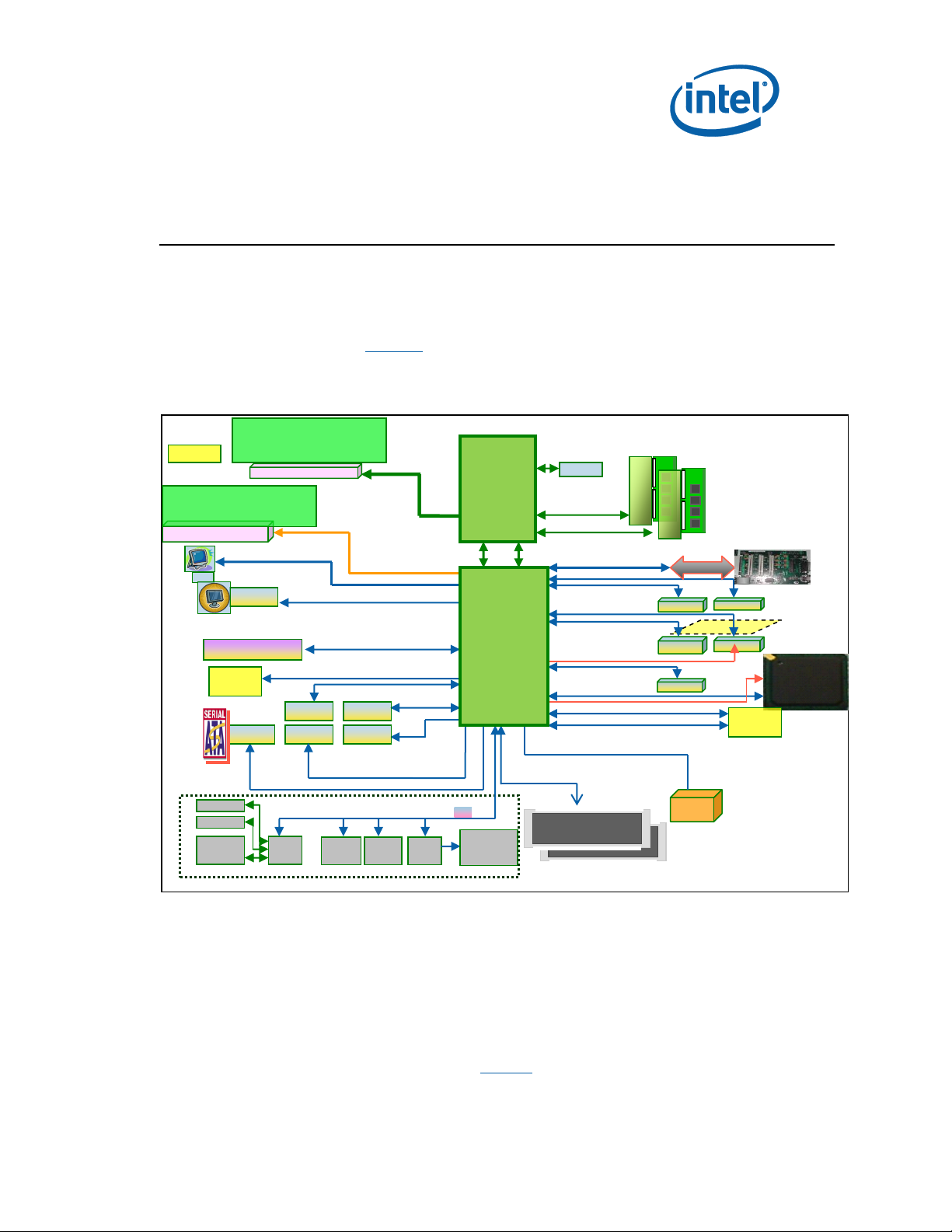
3.1 Block Diagram
The block diagram of the Intel® Core™ i7 Processor with Intel® QM57 Express Chipset
Development kit is shown in Figure 1.
Figure 1. System Block Diagram
3.2 Mechanical Form Factor
The development kit conforms to the ATX 2.2 form factor.
3.3 Development Board Features Table
Development kit features are summarized in Table 5.
Dev Kit Manual 21 323094
Page 22
Description
Comments
Processor
Intel® Core™ i5
Soldered to board
Chipset
Intel® 5 Series Chipset
1071 pin BGA footprint
Memory
Two DDR3 DIMM slots
Maximum 8GB of DDR Memory (RAM) of
ECC and non-ECC using 2Gb1 technology
Supports DDR3 frequency of up to
1066MT/s
Notes:
4Gb (x16 width only) technology support is
under investigation
External
Graphics
PCIe* Slot
One x16 PCIe slot supported.
2x8 PCIe* supported through Nowata Add-
in card.
eDP supported through PCI graphics add-in
card
Video
24-bit dual channel LVDS
Interface
Connectors and cables from previous
development kits can be used.
Display Ports
3 – Display port Lanes on Chipset. 1 On-
Board DP Connector. Other 2 ports can be
supported through PCI graphics add-in card.
CRT
On Board right-angled CRT Connector
Similar to the earlier platforms
HDMI
1 On-Board HDMI Connector (Optional
Routing through Display Port D of Chipset).
Three additional HDMI ports are available
through the Eaglemont 2 external card.
PCI
Three 5V PCI slots supported
through PCI extension card.
PCI revision 2.3 compliant (33MHz)
No PCI slots on motherboard, only one
goldfinger on board.
PCI
Express*
8 PCIe lanes
PCI Express 2.0 base revision compliance
Five lanes to x1 PCIe ports
One lane to LAN
Two Lanes to Docking
On-Board
LAN
Intel® 82577 Gigabit Ethernet PHY
BIOS (SPI)
2x SPI flash devices
Support for multi vendor SPI
Support multi package (SOIC-8 and
SOIC-16)
ATA/
Storage
6 SATA Ports
2 Cable Connector and 1 Direct Connect
Connector. 2 eSATA connectors and 1 to
docking. RAID 0/1 support.
Table 5. Development Kit Feature Set Summary
22 323094 Dev Kit Manual
Page 23

Description
Comments
Intel® High
Definition
Audio MDC
Header
Support via interposer Mott
Canyon 4 daughter card (support
via sideband cable)
Soft Audio/Soft Modem
USB
14 USB 2.0/1.1 Ports
1 Quad USB connector
1 dual USB connector on RJ45
8 ports available as FPIOs
Optional routing to docking for USB lane 4
Over Current protection provided in Pairs.
Floater OC7# used as SMC_WAKE_SCI#
LPC
One LPC slot
Includes sideband headers
SMC/KBC
H8S/2117 micro-controller
Two PS/2 ports
One scan matrix keyboard
connector
ACPI compliant
Clocks
CK-505 system
Supports Buffer Through Mode only.
RTC
Battery-backed Real Time Clock
Processor
Voltage
Regulator
IMVP-6.5 for Processor core
IMVP 6.5 Compliant CPU Core and Graphics
Core VRs, Manual Override Option for VIDs
available on both VR Controllers.
Power
Supply
ATX Power Supply
Debug
Interfaces
Processor and Chipset XDP
Port 80 display
On board Processor Chipset XDP Ports
Port 80 Through Add-in card. Four seven-
segment displays
Intel® AMT
support
Intel® Active Management
Technology 6.0
Power
Management
ACPI Compliant
Supported C states: C0, C1, C1E, C3, C6,
C7
Form Factor
ATX 2.2 like form factor
10 layer board – 12” x 11.2”
3.4 Driver Key Features
The driver CD included in the kit contains all software drivers necessary for basic system
functionality for various operating systems. The CD contains the production drivers that were
released in conjunction with the launch of this platform. However, it is possible that these
drivers have been updated since then. Please check for updated drivers at
http://platformsw.intel.com.
Dev Kit Manual 23 323094
Page 24

Note: Software in the kit is provided free by the vendor and is only licensed for evaluation purposes.
Refer to the documentation in your evaluation kit for further details on any terms and
conditions that may be applicable to the granted licenses. Customers using the tools that work
with Microsoft* products must license those products. Any targets created by those tools
should also have appropriate licenses. Software included in the kit is subject to change.
3.5 BIOS Key Features
This development kit ships with AMI* BIOS pre-boot firmware from AMI* preinstalled. AMI*
BIOS provides an industry-standard BIOS on which to run most standard operating systems,
including Windows* XP/XP Embedded, Linux*, and others.
The following features of AMI* BIOS are enabled in the development board:
DDR3 detection, configuration, and initialization
Intel
POST codes displayed to port 80h
PCI/PCI Express* device enumeration and configuration
Integrated video configuration and initialization
Super I/O configuration
Active Management Technology
Intel
®
QM57 Chipset configuration
®
Matrix Storage Manger RAID 0/1 Support
3.6 System Thermal Management
The objective of thermal management is to ensure that the temperature of each component is
maintained within specified functional limits. The functional temperature limit is the range
within which the electrical circuits can be expected to meet their specified performance
requirements. Operation outside the functional limit can degrade system performance and
cause reliability problems.
The development kit is shipped with a heatsink thermal solution for installation on the
Processor. This thermal solution has been tested in an open-air environment at room
temperature and is sufficient for development purposes. The designer must ensure that
adequate thermal management is provided for if the system is used in other environments or
enclosures.
3.7 System Features and Operation
The following section provides a detailed view of the system features and operation of the
development kit. They are divided into the two sections based upon component: the first
section describes the processor‟s features and the following section describes the chipset‟s
features.
24 323094 Dev Kit Manual
Page 25

3.7.1 Processor
The development kit uses the board design, which supports Intel® Core™ i7 processor in a
BGA package (U3E1). This processor is a 2-die package made up of the dual core processor,
graphics processor and integrate memory controller.
3.7.1.1 Processor Voltage Regulators
The development kit implements an onboard IMVP-6.5 regulator for the processor core supply,
which supports PSI (Power Status Indicator). The maximum current that can be supported by
the Core VR is 60 amps.
3.7.1.2 Processor Power Management
The Processor supports C0, C1 C1E, C3, and C6 states. On this platform all the power
management handshake happens over the DMI interface. None of the „Power State‟ status
signals can be observed on the board directly. Some important Power management pins on
the Processor are listed below.
RESET_OBS# This indicates the final handoff which gets the CPU out of RESET. It is
the final signal to go active in the reset sequence.
VCCPWRGOOD_0/1 Input from the indicating that the system rails and clocks are
stable. The Processor is now ready to be brought out of reset.
VTTPWRGOOD Indicates to the Processor that the 1.1VTT rail is stable.
PSI# An output of the Processor indicating to the VR Controller that it can enter a
low current drive mode to improve its efficiency.
IMON This is a Voltage input to the Processor providing information on the CPU
current consumption.
DPRSLPVR (VID7) An output from the Processor to the IMVP Core VR indicating that
the CPU is in a very low power state.
The only way to detect the entry to/exit from the C1/C3 C-States is to read the DMI
transmissions.
3.7.1.3 Manual VID support for CPU VR
The development kit supports manual VID operation for Processor VR. A jumper J2B1<pins
15-16> is provided to enable “VID override” to the CPU VCC Core VR. The intent of this “VID
override” circuit is for ease of debug and testing. The VID0-VID6 signals of CPU have been
brought out from VID0-VID6 pins on the processor package.
Dev Kit Manual 25 323094
Page 26

Figure 2. VID Override Circuit
3.7.1.4 Graphics Core VR
The development kit implements an onboard IMVP-6.5 compliant VR Controller for the
Graphics core supply. The maximum current that can be supported by the core VR is 21 amps.
3.7.1.5 Manual VID Support for Graphics VR
The development kit supports manual VID operation for Graphics VR. A jumper J2C1<pins 12> is provided to enable “GFX VID override” to the Graphics Core VR. The intent of this “VID
override” circuit is for ease of debug and testing. The implementation is similar to the CPU VR
VID over-ride.
3.7.1.6 Memory Support
The development kit supports dual channel DRR3 interface. There are two DDR3 DIMM sockets
(J4V1 and J4V2) on the motherboard. The memory controller supports four ranks of memory
up to 1066MT/s. The maximum amount of memory supported is 8GB of DDR3 memory.
Minimum capacity supported is 512 MB. The on-board thermal sensor is provided for the
DIMMs.
3.7.1.6.1 Compatible DDR3 DIMM Modules
Raw Card A – single rank x8 unbuffered non-ECC
Raw Card B – dual rank x8 unbuffered non-ECC
Raw Card C – single rank x16 unbuffered non-ECC
26 323094 Dev Kit Manual
Page 27

Raw
Card
Version
DIMM
Capacity
DRAM
Device
Technology
DRAM
Organization
# of
DRAM
Devices
# of
Physical
Device
Ranks
# of
Row/Col
Address
Bits
# of
Banks
Inside
DRAM
Page
Size
A
512 MB
512 Mb
64 M x 8
8 1 13/10
8
8K
1 GB
1 Gb
128 M x 8
8 1 14/10
8
8K
2 GB
2 Gb
256M x 8
8 1 15/10
8
8K
B
1 GB
512 Mb
64 M x 8
16 2 13/10
8
8K
2 GB
1 Gb
128 M x 8
16 2 14/10
8
8K
4 GB
2 Gb
256M x 8
16 2 15/10
8
8K
C
256 MB
512 Mb
32M x 16
4 1 12/10
8
8K
512 MB
1 Gb
64 M x 8
4 1 13/10
8
8K
1 GB
2 Gb
128 M x 16
4 1 14/10
8
8K
2 GB
4 Gb1
256M x 16
4 1 15/10
8
8K
D
512 MB
512 Mb
64 M x 8
9 1 13/10
8
8K
1 GB
1 Gb
128 M x 8
9 1 14/10
8
8K
2 GB
2 Gb
256M x 8
9 1 15/10
8
8K
E
1 GB
512 Mb
64 M x 8
18 2 13/10
8
8K
2 GB
1 Gb
128 M x 8
18 2 14/10
8
8K
4 GB
2 Gb
256M x 8
18 2 15/10
8
8K
F
512 MB
512 Mb
32M x 16
8 2 12/10
8
8K
1 GB
1 Gb
64 M x 16
8 2 13/10
8
8K
2 GB
2 Gb
128 M x 16
8 2 14/10
8
8K
4 GB
4 Gb1
256M x 16
8 2 15/10
8
8K
Raw Card D – single rank x8 unbuffered ECC
Raw Card E – dual rank x8 unbuffered ECC
Raw Card F - dual rank x16 unbuffered non-ECC
Table 6. Supported DIMM Module Configurations
Note: 1. 4 Gb technology support is under investigation pending availability of DRAM silicon.
3.7.1.7 Processor PCI Express* Support (PCI Express Graphics)
The processor supports a PCI Express* port, which can be used for PCI Express Graphics
(PEG) or for PCI Express IO. The development kit supports external graphics through this
processor PEG slot, and supports Lane-Reversal of the PEG lanes. However, the motherboard
uses non-reversed routing.
The processor has the capability of using the PCI Express interface in two ways:
1 x16 PCI Express IO (or PEG)
Dev Kit Manual 27 323094
Page 28

STRAP
1
0
CFG0
Single PCI Express*
(default)
PCI Express Bifurcation Enabled
J1D4: IN (1-2)
CFG4
No Display Port connected to
eDP (default)
An External Display Port is
connected
J1D1: IN (1-2)
2 x 8 PCI Express IO (or PEG)
The 2 x 8 slots are supported through the Nowata Add-In Card. Embedded Display Port (eDP)
is supported through the Eaglemont 2 add-in card.
The usage model of the processor‟s PCI Express interface needs to be configured through the
following hardware straps:
Table 7. Hardware Straps for processor PCI Express* Interface Usage
3.7.1.8 Embedded Display Port
Embedded Display Port (eDP) is a feature on Intel® Core™ Processor.
Note: When eDP is enabled, we can only have 1x8 PEG card. eDP lanes are multiplexed over PEG
12:15 lanes from the processor.
1. Insert the PCI graphics add-in-card in the PEG slot (J5C1), not the DDI slot.
2. To enable eDP, you need to “short” the Jumper pins of J1D1 (1-2) on motherboard.
3. Connect the side-band signals on J6D1 on motherboard, via a cable to J3C1 on the PCI
graphics.
4. For the Sideband signals, we have 2 options
5. Connect J6D1 (on motherboard) to J3C1 (on PCI graphics) through a 10-pin cable.
6. Use the BLI connector from LVDS Connector provided to connect it directly at the eDP
Panel.
3.7.1.9 DMI Interface
The Development kit Supports x4 DMI bi-directional lanes between the Processor and Chipset.
The transmissions happen over DMI protocol. Max speed supported is 2.5GT/s. This protocol is
different from the ones on earlier platforms, and has some instructions added.
3.7.1.10 Intel
The development kit supports Intel® FDI, a new interface. On this platform, the GPU is in the
processor and display interfaces are supported through the chipset. The Intel® FDI is a
dedicated link to transmit the display related pixel information over unidirectional 2x4 lane
interfaces. The synchronization signals are directed from chipset to processor.
28 323094 Dev Kit Manual
®
Flexible Display Interface (Intel® FDI)
Page 29

3.7.1.11 Processor Thermals
The processor temperature is communicated to the chipset over the PECI, a single wire
interface. Some important signals are:
1. CATERR# Indicates that the system has experienced a catastrophic error and
cannot continue to operate.
2. PROCHOT# PROCHOT# will go active when the Processor temperature monitoring
sensor detects that the Processor has exceeded the thermal specifications.
3. THERMTRIP# Assertion indicates that the Processor junction temperature has
reached a level beyond which permanent silicon damage may occur.
3.7.1.12 Processor Active Cooling
The development kit supports PWM-based FAN speed control. Fan circuitry is controlled by the
signal CPU_PWM_FAN signal from the EC. A 4-pin header J4C1 is provided to support FAN
speed output measurement for the CPU.
3.7.2 Chipset
The chipset on the development kit is the Intel® 5 Series Chipset. It provides the interface
optimized for the Processor, DMI and a highly integrated I/O hub that provides the interface to
peripherals. The following sections describe the motherboard implementation of the Chipset
features which are listed as below:
8x PCI Express* 2.0 specification ports running at 2.5GT/s
1x PCI Gold-finger slot (for PCI expansion slots)
On-board LAN
6x SATA ports
Support for CRT, LVDS, HDMI, DP and eDP (embedded DP) displays
14xUSB connectors
LPC interface
Serial IrDA port
Support for two SPI flash devices
Subsystem features described in this section refer to socket and connector locations on
motherboard. Socket and connector locations are labeled with a letter-number combination
(for example, the first memory DIMM connector is located at J4V1). Please refer to the
silkscreen labeling on motherboard for socket locations.
3.7.2.1 Chipset PCI Express* Support
The development kit supports five on board PCIe* (x1) slots. The Chipset has a total of 8 PCIe
Base Specification, Rev 2.0 ports running at 2.5GT/s. Of those IO ports 5 have been routed to
x1 connectors on board, 2 to Docking and one to LAN.
Dev Kit Manual 29 323094
Page 30

PCI-E* Port
Default Destination
Optional Destination
1
PCI-E Slot 1 (J6C2)
-
2
PCI-E Slot 2 (J6D2)
(in-line with Slot 1)
3
PCI-E Slot 3 (J7C1)
-
4
PCI-E Slot 4 (J7D2)
-
5
PCI-E Slot 5 (J6C1)
-
6
LAN (EU7M1)
-
7
DOCKING (J9C2)
PCIe SLOT6 (J8C1)
8
DOCKING (J9C2)
-
Intel® QM57
Express
Chipset
GbE LAN
Card
Table 8. PCI Express* Ports
3.7.2.2 PCI Slots
The development kit does not have any PCI slots on the motherboard. Three 5V PCI slots are
supported via PCI Extension Card.
3.7.2.2.1 PCI Gold-Fingers
A gold-finger connector (S9B1) is also supplied on the motherboard, which allows an external
PCI expansion board to connect to motherboard. The PCI expansion board has three
additional PCI slots allowing the user greater expansion. See section Daughter and Plug-in
Cards for more information on the PCI expansion board add-in card.
3.7.2.3 On-Board LAN
The development kit supports 10/100/1000 Mbps Ethernet on board via the Intel® 82577 GbE
PHY. It has a PCI-E and SM-BUS link to the Chipset. Data Transfer happens over PCI-E lanes.
Communication between the LAN Controller and the LAN Connected Device is done through
SMBus whenever the system is in a low power state (Sx). LAN is also supported over
DOCKING.
A block Diagram of the implementation is given in Figure 3.
Figure 3. Block Diagram of On-board LAN Implementations
30 323094 Dev Kit Manual
Page 31

I/O Voltage for the High
Definition Audio
STUFF
NO STUFF
3.3V (Default)
R8R11, R8R9
R8R10, R8E1
SATA Port
Connection Type
Connector
Port 0
Direct Connect
J8J1
Port 1 and Port 2
Cable Connect
J7G2 and J7G1
Port 3 and Port 4
eSATA
J6J1 and J7J1
3.7.2.4 Soft Audio/ Soft Modem
Intel® High Definition Audio functionality (Intel® HD Audio) is enabled through the Mott
Canyon 4 daughter card. The Chipset supports four Intel HD Audio CODECs. All four are routed
to MDC header through resistor stuffing options. By default CODEC 0 and 1 will be connected
to the MDC card. An on-board header is provided at J9E7 and J9E4 for this purpose. No direct
connection is provided for the Intel® High Definition Audio Card on the motherboard; the Mott
Canyon 4 card is required to enable the Intel HD Audio functionality. See Section 5 for more
information on the Mott Canyon 4 card.
The motherboard supports low voltage (LV) high definition I/O CODEC. Resistor stuffing
options are used to select between 3.3V I/O and 1.5VI/O.
Table 9. Selection of I/O Voltage for the Intel® High Definition Audio
3.7.2.5 SATA Storage
Table 10. SATA Ports
These connectors mentioned in Table 10 are for the serial data signals. The motherboard has a
power connector J8J1 to power the serial ATA hard disk drive. A green LED at CR7G1
indicates activity on SATA channel.
The motherboard shares the power connector for both SATA 1 and 2. Due to this only one of
the serial ATA channel (Port1 by default) supports the hot swapping capability. Hot swap on
Port 1 can be used only when the Port 2 is not used. A Y-Power cable needs to be connected
first to the device on Port 1 before connecting the signal cable. When hot swap is not desired,
both Port 1 and Port 2 can be used. A jumper J7H1 is provided to enable hot plug/removal on
port-1.
The eSATA drives should be externally powered. Hence, there is no power supply support for
them on the motherboard.
3.7.2.6 USB Connectors
The Chipset provides a total of 14 USB 2.0/1.1 ports.
Dev Kit Manual 31 323094
Four ports (0, 1, 2, and 3) are routed to a four-stacked USB connector (J3A3) at the
back panel.
Two USB ports (8 and 9) are routed to a RJ45 + Dual USB Connector (J4A1) on the
back of the chassis.
Page 32

USB Port
Panel
Connector
Port 0
Back Panel I/O Connector
J3A3 (4 stacked USB Connector)
Port 1
Back Panel I/O Connector
J3A3 (4 stacked USB Connector)
Port 2
Back Panel I/O Connector
J3A3 (4 stacked USB Connector)
Port 3
Back Panel I/O Connector
J3A3 (4 stacked USB Connector)
Port 4
FPIO
J8H1 (2x5 Connector)
Port 5
FPIO
J8H1 (2x5 Connector)
Port 6
FPIO
J7H3 (2x5 Connector)
Port 7
FPIO
J7H3 (2x5 Connector)
Port 8
Back Panel
J4A1
Port 9
Back Panel
J4A1 (Rework Required: Stuff R8F3 and
R8F5; No Stuff R8F2 and R8F4)
Port 10
FPIO
J7H4 (2x5 Connector)
Port 11
FPIO
J7H4 (2x5 Connector)
Port 12
FPIO
J7H2 (2x5 Connector)
Port 13
FPIO
J7H2 (2x5 Connector)
IO headers are provided for the other 8 USB lanes.
Over current protection has been provided for ports in pairs. Ports (0,1), (1,2)…(12,13) share
the OC Indicators.
Table 11. USB Port Mapping
3.7.2.7 LPC Super I/O (SIO)/ LPC Slot
A SMSC SIO1007 serves as the SIO on the motherboard and is located at U9A1. Shunting the
jumper at J8C3 to the 2-3 positions can disable the SIO by holding it in reset. This allows
other SIO solutions to be tested in the LPC slot at J8F2. A sideband header is provided at
J9G2 for this purpose. This sideband header also has signals for LPC power management.
3.7.2.8 Serial IrDA
The SMSC SIO incorporates a serial port, and IrDA (Infrared), as well as general purpose IOs
(GPIO). The Serial Port connector is provided at J1A2, and the IrDA transceiver is located at
U6A2. The IrDA transceiver on the motherboard supports SIR (slow IR), FIR (Fast IR) and
CIR (Consumer IR). The option to select between these is supported through software and
GPIO pin (IR_MODE) on the SIO.
3.7.2.9 System Management Controller (SMC)/ Keyboard
Controller (KBC)
A Renesas* H8S/2117 (U9H1) serves as both SMC and KBC for the platform. The SMC/KBC
controller supports two PS/2 ports, battery monitoring and charging, wake/runtime SCI
32 323094 Dev Kit Manual
Page 33

MODE
J8D1
J8D3
J8D2
Normal
Operation
1-X
1-X
3-X
1-X
Programming
SPI0
1-2
1-2
3-X
1-2
Programming
SPI1
1-2
1-X
2-3
1-2
events, CPU thermal monitoring/Fan control, GMCH thermal throttling support, LPC docking
support and power sequencing control.
The two PS/2 ports on motherboard are for legacy keyboard and mouse. The keyboard plugs
into the bottom jack and the mouse plugs into the top jack at J1A1. Scan matrix keyboards
can be supported via an optional connector at J9E3.
There is a LPC Slot (J8F2) and LPC Sideband connector (J9G2) on board to connect external
EC for validation purposes. On-board EC has to be disabled by shorting pin 1 and 2 of
connector J9F2 and an external EC has to take care of board power sequencing and thermal
management.
If the intention is just to read thermal information from the Chipset by external EC/Fan
controller, only Chipset SM-Bus signals (SML1_CLK and SML1_DATA) from the LPC sideband
connector can be used without connecting the EC on LPC slot.
For more information on the embedded controller please refer to Intel® Management Engine
(Intel® ME) and Embedded Controller Interaction for Intel® Core™ i7 Processor Based LowPower Platform.
3.7.2.10 SPI
The Serial Peripheral Interface (SPI) on Intel® QM57 Express Chipset can be used to support
two compatible flash devices (U8C1 and U8D1), storing Unified BIOS Code. The SOIC-8
package (U8D2 and U8C2) would support 16 Mb SPI flashes, while the SOIC-16 (U8C1 and
U8D1) package will support 32Mb or higher SPI flash. One can opt to use SPI sockets, if they
wish to. Socket KOZ has been taken into account in the Layout. A Dediprog Header (J8E1) has
been provided for SPI Programming.
Note: Out of the SOIC-8 and SOIC-16 footprints supported on the board only one of these can be
used at a time and on the board. Footprint is arranged one over the other. By default, U8C1
(16Mb on CS#0) and U8D1 (16Mb on CS#1) will be stuffed.
Table 12. Jumper Setting for SPI Programming
3.7.2.11 Clocks
The development kit system clocks are provided by the CK505 (EU6V1) clock synthesizer.
The BCLK frequency can be set using the BSEL Jumpers J6G1, J6F2, J6F3. Unlike previous
platforms it always needs to be 133MHz.
Dev Kit Manual 33 323094
Page 34

CPUSTP# is not supported as the requirement is to have this clock always running during
buffered mode.
Figure 4. BCLK Frequency Select Circuit
The clocks on the motherboard are provided by the chipset which uses four clocks from CK505
as inputs and use these as a reference to generate all the other platform clocks. A general
block diagram is shown in Figure 5.
34 323094 Dev Kit Manual
Page 35

Intel® QM57
Express
Chipset
Figure 5. Platform Clocking Circuit
3.7.2.12 Real Time Clocks (RTC)
An on-board battery at BT5G1 maintains power to the real time clock (RTC) when in a
mechanical off state. A CR2032 battery is installed on the motherboard.
Warning: There is a risk of explosion if the lithium battery is replaced by an incorrect type. Dispose
of used batteries according to the vendor's instructions.
3.7.3 Displays
The development kit supports the following displays:
1. CRT: A right angled CRT connector has been provided on board (J1A2). Optional
routing to the docking connector is supported through a CRT dock switch (U6C1).
2. LVDS: LVDS support is very similar to the one on earlier platforms. Connector is at
J7D3.
3. HDMI: A HDMI connector (J3A2) is added on-board for the first time. HDMI
connectors are also available on PCI graphics add-in-card.
4. DP: A DP connector (J5A1) has been added on board for the first time. DisplayPort
connectors are also available on PCI graphics add-in-Card.
5. eDP: eDP is available on the PCI graphics add-incard. When used for eDP, this card
needs to be inserted in the PCIe Slot (J5C1) and not in the DDI Slot (J8C2). A 2x5
header (J6D1) is provided for the side-band signals (backlight related information and
SMBUS access).
Dev Kit Manual 35 323094
Page 36

Note: A maximum of two displays can be active at a time.
Note: Display connectors DP/HDMI are on Port D of Chipset, Port B and C can be used through PCI
graphics add-in-card.
6. One DP and one HDMI Connector have been provided on board on the motherboard.
Port D of Digital Display Interface on PCH is mapped to on board DP and HDMI connectors.
DP is the default configuration. To select HDMI rework is required on the motherboards.
For HDMI:
a. No stuff – C5A1, C5A2, C5A13, C5A14, C5A5, C5A6, C5A9, C5A10
b. Stuff – C5A3, C5A4, C5A15, C5A16, C5A7, C5A8, C5A11, C5A12 with 0402 0.1 µF
capacitor
c. The same capacitors no stuffed in Step A can be used in Step B
i. R2M2 and R2M5 are the 2.2k pull-ups on SMBus. These should be changed to
4.4 k
ii.
3.7.3.1.1 Digital Display Interface Configuration Modes
1. 3x DisplayPorts
2. 3x HDMI/DVI Ports
3. 2x DP + 1x SDVO
4. 2x DP + 1x HDMI/DVI
5. 2x HDMI/DVI + 1x SDVO
6. 2x HDMI/DVI + 1x DP
7. 1x DP + 1x HDMI/DVI + 1x SDVO
36 323094 Dev Kit Manual
Page 37

Processor
Chipset
DMI
FDI
DPC
Primary Slot
GPIO
from
H8
Secondary Slot
Add-in-Card
DP
MUX
x16 PCIe Connector
x16 PCIe Connector
DPC
1x16 PCIe (0:15)
To
Docking
DPD
HDMI
LVL
TRAN
DP
VGA
Connector
LVDS
Connector
To
Back
Panel
Resistor Strapping
Default Option (Solid Line)
Optional (Dashed Line)
Figure 6. Intel® Core™ i7 Processor Based Low-Power Platform Display Interfaces
3.7.3.1.2 DP/HDMI Support
One DP and one HDMI Connectors have been provided on board.
1. Port D of Digital Display Interface on the chipset is mapped to on board DP and HDMI
connectors.
2. DP is the default configuration. To select HDMI rework is required on the
motherboards.
3. For HDMI:
a. No stuff – C5A1, C5A2, C5A13, C5A14, C5A5, C5A6, C5A9, C5A10.
b. Stuff – C5A3, C5A4, C5A15, C5A16, C5A7, C5A8, C5A11, C5A12 with 0402 0.1 uF
capacitor.
c. The same capacitors no stuffed in Step A can be used in Step B.
i. R2M2 and R2M5 are the 2.2k Pull-ups on SMBUS. These should be changed to
4.4K.
ii. For HPD: Stuff R5A1 with 0 ohms and No stuff R5A2.
3.7.3.2 Firmware Hub (FWH) support
Note: The development kit does not support a FWH on the board.
Dev Kit Manual 37 323094
Page 38

State
Description
G0/S0/C0
Full on
G0/S0/C3
Deep Sleep: CPUSTP# signal active
G1/S3
Suspend To RAM (all switched rails are turned off)
G1/S4
Suspend To Disk
G2/S5
Soft Off
G3
Mechanical Off
3.7.3.3 Power Supply Solution
The motherboard contains all of the voltage regulators necessary to power the system up.
Note: Use an “ATX12V” 1.1 Spec compliant power supply (an "ATX12V" rating means V5 min current
=0.1 A, "ATX" V5 min current = 1.0 A, among other differences).
Note: If the power button on the ATX power supply is used to shut down the system, wait at least
five seconds before turning the system on again. We do not recommend shutting down the
system this way.
3.7.4 Debugging Interfaces
3.7.4.1 Processor Debug
An XDP (Extended Debug Port) connector is provided at J1D3 for processor run control debug
support.
A port 80-83 display add-in card can also be used for debug. The port 80-83 add in card could
be used on the TPM header located at J9A1.
3.7.4.2 Chipset Debug
An XDP Connector is provided at J8H3, for chipset debug support.
3.7.5 Power Management
3.7.5.1 Power Management States
Table 13 lists the power management states. The Controller Link (CL) operates at various
power level, called M-states. M0 is the highest power state, followed by M3 and M-off.
Table 13. Power Management States
3.7.6 Power Measurement Support
Power measurement resistors are provided on the platform to measure the power of most
subsystems. All power measurement resistors have a tolerance of 1%. The value of these
38 323094 Dev Kit Manual
Page 39

R
V
P
2
EXAMPLE SYSTEM
Sense Resistor Value:
0.002Ω
Voltage Difference Across Resistor:
1.492mV (746mA)
Calculated Power:
1.113mW Agilent 34401A (6 ½ digit display)
Fluke 79 (3 digit display)
Specification:
(±0.0030% of
reading)
+ (±0.0030% of
range)
Specification:
±0.09% ±2 digits
Min Voltage Displayed:
Calculated Power:
1.49193mV
1.1129mW
Min Voltage Displayed:
Calculated Power:
1.47mV
1.08mW
Max Voltage Displayed:
Calculated Power:
1.49206mV
1.1131mW
Max Voltage Displayed:
Calculated Power:
1.51mV
1.14mW
Error in Power:
±0.009%
Error in Power:
±0.3%
Voltage Rail Name
REFDES of the
Power Measurement Resistor
GVR_VBAT
R1E2
+VGFX_CORE
R2D11
power measurement resistors are 2mOhm by default. Power on a particular subsystem is
calculated using the following formula:
It is recommended that the user use a high precision digital multimeter tool such as the
Agilent* 34401A digital multi-meter. Refer to Table 14 for a comparison of a high precision
digital multi-meter (Agilent 34401A) versus a standard precision digital multimeter (Fluke*
79).
Table 14. Digital Multimeter
R = value of the sense resistor (typically 0.002Ω)
V = the voltage difference measured across the sense resistor.
As Table 14 shows the precision achieved by using a high precision digital multimeter versus a
standard digital multimeter is ~33 times more accurate.
The Power Measurement resistors provided for the various rails are listed in Table 15:
Table 15. Power Measurement Resistor for Power Rails
Dev Kit Manual 39 323094
Page 40

Voltage Rail Name
REFDES of the
Power Measurement Resistor
+VDC_PHASE
R3B23
+V1.05S_PCH_VCC
R6U15
MAX8792_V1.05SVTT_LX_L
R4F1
MAX8792_V1.05M_LX_L
R6E8
+V5S_HDMID_OB
R2A2
1.5_VIN
R3W26
+V3.3S_DP_OB
R5N1
+V5A_USBPWR_IN
R3A1
+V1.05S_VCC_SA
R4D10
+V3.3A_MBL
R4H1
+V1.8S_VCCSFR
R4D4
MAX8792_V1.1SVTT_VIN
R5G1
+V1.05S_VCCTT
R4R2
-V12A
R4H7
+V5SB_ATXA
R4H8
+V1.05S_VCC_PEG_DMI
R4D9
+V1.8S
R5E1
+V12S_PEG
R5N2
+V3.3S_PEG
R5C2
62290_VIN
R5E5
+V12S_SATA_P1
R5W9
+V3.3S_PCIESLOT2
R6P1
+V3.3S_PCIESLOT1
R6B5
+V12S_PCIESLOT1
R6B2
+V12S_PCIESLOT5
R6N1
MAX8792_V1.05M_VIN
R6T4
+V5S_LVDS_BKLT
R7D11
+V3.3_PCIESLOT3
R7C1
+V3.3_PCIESLOT4
R7R2
+V12S_PCIESLOT3
R7N1
+V3.3S_PCIESLOT5
R7B6
+V3.3M_LAN
R7A1
+V3.3S_LVDS_DDC
R7R12
+V12S_PCIESLOT4
R7P5
40 323094 Dev Kit Manual
Page 41

Voltage Rail Name
REFDES of the
Power Measurement Resistor
+V5S_SATA_P1
R7W1
+V1.05M_VCCEPW
R7T26
+VDD_VDL
R7D3
+V3.3S_1.5S_HDA_IO
R8R9
+VCC_LVDS_BKLT
R8D1
+V3.3S_PCIESLOT6
R8C1
+V12S_PCIESLOT6
R8B1
+V5_LPCSLOT
R8T8
+V5_PS2
R8N1
+V3.3_LPCSLOT
R8U1
+V3.3A_1.5A_HDA_IO
R8R11
+V3.3A_KBC
R8H13
+V3.3S_VCCPPCI
R8U3
+V3.3M_SPI
R8R5
+V3.3S_IR
R8M4
+V3.3S_DPS
R8B4
+V12S_DPS
R8N4
+V5S_SATA_P0
R8H15
+V12S_SATA_P0
R8W23
+V3.3S_SATA_P0
R8Y1
+V12S_PCI
R9N1
+V3.3S_PCI
R9D1
+V5S_PCI
R9B5
+V5_R1_TPM
R9M6
+V3.3S_R1_TPM
R9M8
+V3.3A_R1_TPM
R9M9
+V0.75S_R
R3W19
51125_V3.3A_VBATA
R4V11
+VDDIO_CLK
R5H1
51125_V5A_VBATA
R5W1
+V5A_MBL
R5H4
+V12S_PCIESLOT2
R6C14
+V3.3S_NVRAM
R6V18
+VDD_CK505
R6W17
Dev Kit Manual 41 323094
Page 42

Voltage Rail Name
REFDES of the
Power Measurement Resistor
+V3.3S_SATA_P1
R6W18
+V1.1S_VCC_SATA
R7V2
+V3.3S_SIO
R9M10
+V3.3_KBCS
R9E6
51125_VIN
R5G6
+V5S_IMVP6
R3B20
+V3.3S_DIMM1
R2G15
+V3.3S_DIMM0
R2G4
+V1.05S_VCC_DMI
R6U19
+VCCA_DPLL_L
R6E9
+V3.3S_VCCA3GBG
R6U10
+V3.3S_CRT_VCCA_DAC
R7E15
+V3.3M_VCCPEP
R7U17
+V_NVRAM_VCCPNAND
R7V1
+V1.0M_LAN
R7A8
+V3.3A_VCCPUSB
R7F3
+V1.5S_1.8S_VCCADMI_VRM
R6U11
+VCCAFDI_VRM
R6U13
+VCCPLLVRM
R6U14
+V1.1S_PCH_VCCDPLL_EXP
R6U16
+V1.05S_VCCPCPU
R6U17
+V1.05S_VCCDPLL_FDI
R6F14
+V3.3M_LAN_OUT_R
R7A10
+V1.05S_VCCUSBCORE
R7F4
+V1.8S_VCCTX_LVD
R7T33
+V3.3S_VCCA_LVD
R7U1
+V3.3S_VCC_GIO
R7U2
+V1.05S_SSCVCC
R7T14
+V3.3A_1.5A_VCCPAZSUS
R7U8
+V1.05M_VCCAUX
R7U9
+V3.3S_VCCPCORE
R7U11
+V3.3A_VCCPSUS
R8F12
42 323094 Dev Kit Manual
Page 43

3.7.7 Power Supply Usage and Recommendation
As the Desktop ATX supplies grew to meet the increased power for those motherboards, their
minimum loading requirements also grew. When running a mobile platform on it, it may not
load the 5.0V rail enough to meet the minimum loading requirements for it to maintain
regulation. The power supply is included as a part of the development kit.
Warning: DO NOT use Delta* or PowerMan ATX* supplies. You may experience the following
symptoms when using a non-Sparkle supply.
"post 00"
Blue screen reporting driver or device issue when using a desktop PCI graphics card
Hanging during boot with PCIe or PCI graphics
PCI video only during boot, but not available after in Windows*
Dev Kit Manual 43 323094
Page 44

4 Development Board Physical
Hardware Reference
This section provides reference information on the physical hardware, including component‟s
locations, connector pinout information and jumper settings.
4.1 Primary Features
Figure 7 and Figure 8 show the major components of the motherboard, top and bottom views
respectively). Table 16 gives a brief description of each component.
Figure 7. Component Locations – Top View
44 323094 Dev Kit Manual
Page 45

Item
Description
1
SMSC IO
2
PCIe* Slot 6 (No_Stuff)
3
Infra red port
4
LAN Docking switch
5
PCIe Slot3
6
PCIe Slot 4
Figure 8. Component Locations – Bottom View
Table 16. Component Location
Dev Kit Manual 45 323094
Page 46

Item
Description
7
PCI-e Slot 5
8
DP Docking Switch
9
RS232 Transceiver
10
PCIe Slot 1
11
PCIe Slot 2
12
Chipset JTAG Buffer
13
Onboard display port
14
HDMI LVL translator
15
Onboard HDMI port
16
CPU core VID Override jumper
17
GFx core VID Override jumper
18
Processor XDP
19
CPU heat sink on top of the
Processor
20
Power Button
21
Reset button
22
Processor
23
AC Jack
24
System VR
25
Front Panel Header
26
RTC Battery holder
27
USB FPIOs
28
USB FPIOs
29
Chipset XDP
30
Virtual Battery Switch
31
EC/KSC
32
Lid Switch
33
Virtual docking Switch
34
LPC Slot
35
Chipset
36
LPC side band
37
Scan Matrix
38
LPC Hot Dock
39
SPI Programming Header
40
SPI Devices
46 323094 Dev Kit Manual
Page 47

Item
Description
41
PCI gold finger
42
TPM Header
43
Intel 82577 LAN PHY
44
CK 505
45
DMI LAI
46
FDI LAI
47
DDR3 VR
48
I2C Port Hub
Item
Connector
Description
1
J8C2
Chipset DDI port x16 connector
2
J5C1
PCI Express x16 connector
3
J5B1
Chipset JTAG Header
4
J4A1B
RJ45 USB connector
4
J3A3
Quad USB connector
6
J1A1
PS/2 Keyboard/mouse connector
7
J1H2
Battery A connector
8
J1H1
Battery B connector
10
J4H1
ATX Power Supply connector
11
J6J1
eSATA connector 1
12
J7J1
eSATA connector 2
13
J8J1
SATA Direct connect
14
J7D3
LVDS connector
15
J9E4/ J8F1
HDA connector
16
J9C2
Docking connector
4.2 Connectors
Caution: Many of the connectors provide operating voltage (+5 V DC and +12 V DC, for example) to
devices inside the computer chassis, such as fans and internal peripherals. Most of these
connectors are not over-current protected. Do not use these connectors for powering devices
external to the computer chassis. A fault in the load presented by the external devices could
cause damage to the computer, the interconnecting cable, and the external devices
themselves. This section describes the board‟s connectors.
Table 17 lists the connectors on the motherboard.
Table 17. Connectors on the motherboard
Dev Kit Manual 47 323094
Page 48

Item
Connector
Description
17
U3E1C
DDR Channel 1
18
U3E1D
DDR Channel 2
Item
Description
Ref
Des
Item
Description
Ref Des
1
Display Port
J5A1
5
HDMI Connector
J3A2
2
RJ-45 USB Ports
J4A1
6
CRT RS-232
J1A2
3
Quad-stack USB
J3A3
7
PS2- Mouse on Top
J1A1
4
DP Connector
J5A1
Reference
Designator
Function
Default Setting
Optional Setting
J4B1
ON BOARD DDR3 THERMAL SENSOR
IN: To Processor
OUT: Disconnected
J4B2
ON BOARD DDR3 THERMAL SENSOR
IN: To Processor
OUT: Disconnected
J1D4
PCIe Configuration Select
OUT: Single PCIe
IN: Bifurcation enabled
J1D1
DISPLAY PORT PRESENT
OUT: Disabled; No
Physical Display
Port attached
IN: Enabled; An external
display Port device is
connected
J1J2
PM_EXTTS CONTROLLER
2-3: To EC
1-2: To Processor
J5F2
CMOS SETTING
OUT: Save CMOS
IN: Clear CMOS
2 6 3
7 5 1
4.2.1 Back Panel Connectors
Figure 9. Back Panel Connector Locations
Table 18. Back Panel Connectors
4.3 Configuration Settings
Caution: Do not move jumpers with the power on. Always turn off the power and unplug the power
cord from the computer before changing jumper settings. It may damage the board.
Table 19. Configuration Jumper/Switches Settings
48 323094 Dev Kit Manual
Page 49

Reference
Designator
Function
Default Setting
Optional Setting
J5F1
TPM SETTING
OUT: Save ME RTC
Register
IN: Clear ME RTC Register
J9E1
TPM FUNCTION
OUT: Disabled
IN: Enable
J9G4
NO REBOOT
OUT: Disabled
IN: Enabled
J6B1
PCH_JTAG_RST#
IN: Logic Low
OUT: Logic High
J6E1
MPC SWITCH CONTROL
OUT: MPC Off
IN: MPC On
J9E6
BBS STRAP
OUT: Logic High
IN: Logic Low
J8F3
CONFIGURABLE CPU OUTPUT
BUFFER
OUT: Logic High
IN: Logic Low
J8F7
motherboard/SV DETECT
OUT: Logic Low
IN: Logic High
J8G1
BIOS RECOVERY
OUT: Logic High
IN: Logic Low
J2A1
HDMI LEVEL SHIFTER ENABLED
IN: Logic Low
OUT: Logic High
J7B2
PCIE SLOT 3 POWER CONTROL
2-3: V3.3S
1-2: V3.3_VAUX
J7D1
PCIE SLOT 4 POWER CONTROL
2-3: V3.3S
1-2: V3.3_VAUX
J9H5
SATA DEVICE STATUS
IN: Logic Low
OUT: Logic High
J9G3
PLL ON DIE VOLTAGE REGULATOR
ENABLE
OUT: Enabled;
Logic High
IN: Disabled; Logic Low
J7H1
SATA HOT PLUG REMOVAL DEFAULT
SUPPORTED
IN: Supported
OUT: Not Supported
J9H3
SATA DEVICE STATUS
IN: Logic Low
OUT: Logic High
J8D1
SPI PROGRAMMING
OUT: Normal
Operations
1-2: Programming SPI0 or
SPI1
J8D3
SPI PROGRAMMING
ALL OUT: Normal
Operations
1-2/3-X: Programming
SPI0
1-X/2-3: Programming
SPI1
J8D2
SPI PROGRAMMING
OUT: Normal
Operations
1-2: Programming SPI0 or
SPI1
J9E2
SPI PROGRAMMING
1-2: DEFAULT
2-3: Connected to
SPI_CS2#
J6F2
BCLK FREQUENCY SELECTION
IN: Logic High
OUT: Logic Low
J6F3
BCLK FREQUENCY SELECTION
IN: Logic Low
OUT: Logic High
J6G1
BCLK FREQUENCY SELECTION
IN: Logic Low
OUT: Logic High
J8C3
SIO RESET
1-2: Default
2-3: Logic Low - Reset
J7B1
RS232 PORT FOR EC FIRMWARE
DEBUG
OUT: Default
1-2: R2IN Logic Low
2-3: T2OUT Logic Low
J6A3
IN CKT H8 PROGRAMMING
1-2: Normal
2-3: Remote Programming
J6A2
IN CKT H8 PROGRAMMING
1-2: Normal
2-3: Remote Programming
Dev Kit Manual 49 323094
Page 50

Reference
Designator
Function
Default Setting
Optional Setting
J8G5
H8 MODE SELECTION
IN: Logic Low
OUT: Logic High
J8G4
H8 MODE SLECTION
OUT: Logic High
IN: Logic Low
J9F2
SMC/KSC
OUT: On board EC
Enabled
IN: On board EC Disabled
J8G6
KBC CORE DEBUG
OUT: Enabled
IN: Disabled
J9F1
THERM STRAP
OUT: Enabled
IN: Disabled
J9H1
SWITCHABLE GFX
OUT: Disabled
IN: Enabled
J9H4
SMC LID
OUT: Enabled
IN: Disabled
J9H2
VIRTUAL BATTERY
OUT: Enabled
IN: Disabled
J9G1
BOOT BLOCK PROGRAMMING
IN: Normal
OUT: Remote
Programming
J1C2
GFX VR ENABLE
OUT: Default
IN: Logic Low
J4J1
G3 SUPPORT
1-X: No After_G3
support
1-2: After G3 support with
ATX supply
2-3: After G3 Support
with AC brick
J1F1
FORCE POWER UP VBAT
OUT: Logic High
IN: Logic Low
J1E1
FORCE SHUT DOWN
OUT: Logic Low
IN: Logic High
J6A1
CON3_HDR
1-2: SML0_CLK Logic Low
2-3: SML0_DATA Logic
Low
J8H2
SGPIO
OUT: Logic High
1-2: Logic Low
2-3: Not used
J2B1
VID Override
OUT: Logic High
IN: Logic Low
15-16: Enable VID
Override
13-14: VID0
11-12: VID1
9-10: VID2
7-8: VID3
5-6: VID4
3-4: VID5
1-2: VID6
J2C1
GFX VID Override
OUT: Logic High
IN: Logic Low
15-16: VID6
13-14: VID5
11-12: VID4
9-10: VID3
7-8: VID2
5-6: VID1
3-4: VID0
50 323094 Dev Kit Manual
Page 51

Reference
Designator
Function
Default Setting
Optional Setting
1-2: Enable Gfx VID
Override
J8H1
USB Header 1 – Port 4 and Port 5 –
PCIe Slot 1 and Slot 2
1-3: USBP4N connected
2-4: USBP5N connected
5-7: USBP4P grounded
6-8: USBP5P grounded
9-10: no connect
J7H3
USB Header 2 – Port 6 and Port 7 –
PCIe Slot 3 and Slot 4
1-3: USBP6N connected
2-4: USBP7N connected
5-7: USBP6P grounded
6-8: USBP7P grounded
9-10: no connect
J7H4
USB Header 3 – Port 10 and Port 11
1-3: USBP10N connected
2-4: USBP11N connected
5-7: USBP10P grounded
6-8: USBP11P grounded
9-10: no connect
J7H2
USB Header 4 – Port 12 and Port 13
1-3: USBP12N connected
2-4: USBP13N connected
5-7: USBP12P grounded
6-8: USBP13P grounded
9-10: no connect
J8F4
Flash Descriptor Security Override
7-9: Logic Low
Out: Logic High
J1E2
Reserved
No Stuff
J3B1
Reserved
No Stuff
J3B2
Reserved
No Stuff
Note: A jumper consists of two or more pins mounted on the motherboard. When a jumper cap is
placed over two pins, it is designated as IN or 1-2. When there are more than two pins on the
jumper, the pins to be shorted are indicated as 1-2 (to short pin 1 to pin 2), or 2-3 (to short
pin 2 to pin 3), etc. When no jumper cap is to be placed on the jumper, it is designated as
OUT or 1-X.
4.4 Power On and Reset Push Buttons
The motherboard has two push-buttons, POWER and RESET. The POWER button releases
power to the entire board causing the board to boot. The RESET button forces all systems to
warm reset. The two buttons are located near the Processor (Marked as #3 in Table 20) close
to the East edge of the board. The POWER button is located at SW1E1 (Marked as #1 in Table
20) and the RESET button is located at SW1E2 (Marked as #2 in Table 20).
Dev Kit Manual 51 323094
Page 52

Item
Description
Ref
Des
1
Power Button
SW1E1
2
Reset Button
SW1E2
3
CPU
U3E1
Function
Reference
Designator
Page# on the
Schematics for
reference
SATA ACTIVITY
CR7G1
16
MPC ON/OFF Indicator
CR6D1
18
BRAIDWOOD R/B#
CR7G2
27
VID0
CR1B1
46
VID1
CR1B2
46
VID2
CR1B3
46
VID3
CR1B4
46
VID4
CR1B5
46
VID5
CR1B6
46
VID6
CR1B7
46
NUM LOCK
CR9G2
47
CAPS LOCK
CR9G3
47
SCROLL LOCK
CR9G1
47
S4
CR5G6
65
S5
CR5G7
65
M0/M3
CR5G3
65
S3 COLD
CR5G5
65
S0
CR5G4
65
DSW
CR5G2
65
SYSTEM POWER GOOD
CR5G8
65
Table 20. Power-on and Reset Push Buttons
4.5 LEDs
The following LEDs in Table 21 provide status of various functions:
Table 21. Development lit LEDs
52 323094 Dev Kit Manual
Page 53

Signals
SMC_INITCLK (H8
NMI)
Serial Port (TXD)
Serial Port (RXD)
Jumper setting
Open (Default: 1-x)
Short pin 2 and 3
(Default: 1-2)
Short pin 2 and 3
(Default: 1-2)
Motherboard
J7B1
J6A2
J6A3
4.6 Other Headers
4.6.1 H8 Programming Header
The microcontroller firmware for system management/keyboard/mouse control can be
upgraded in two ways. The user can either use a special DOS* utility (in-circuit) or use an
external computer connected (remote) to the system via the serial port on the board.
If the user chooses to use an external computer connected to the system via the serial port,
there are four jumpers that must be set correctly first. Please refer to Table 12 for a summary
of these jumpers.
Required Hardware: One Null Modem Cable and a Host Unit with a serial COM port (System
used to flash the SUT)
Here is the sequence of events necessary to program the H8:
1. Extract all files (keep them in the same folder) to a single directory of your choice on
the host machine or on a floppy disk (recommended).
2. Connect a NULL modem cable to the serial ports of each platform (host and unit to be
flashed).
3. Boot host in DOS mode.
4. Set the jumpers on the motherboard as in Table 22.
5. Power on the motherboard and press the PWR button.
6. From the host directory where you extracted the files, run the following command
line:
KSCFLAxx ksc.bin / Remote
xx refers to the KSC flash utility version number.
Note: This file will program ksc.bin to the KSC flash memory through the remote (Null modem
cable).
7. Follow the instructions that the flash utility provides.
8. After successful programming of the KSC, switch-off motherboard power and move all
three jumpers back to their default setting. The program assumes the host computer
is using serial port 1.
Note: Make sure the board is not powered on, and the power supply is disconnected before moving
any of the jumpers.
Table 22. H8 Programming jumpers
4.6.2 Expansion Slots and Sockets
Table 23 is a list of the slots and sockets available for attaching additional devices.
Dev Kit Manual 53 323094
Page 54

Reference
Designator
Slot/Socket Description
Detail
J4C1
Fan Connector
Table
24_Front_Panel_Header
J5J1
Front Panel Header
Table 25
J5D1
eDP Support
Table 26
J8J1
SATA „Direct Connect‟ Connector
Table 27
J7G2, J7G1,
J6J1, J7J1
SATA Signal Connectors
Table 28
J6H1
SATA Power Connector
Table 29
J8E1
SPI Programming Header
Table 30
J9E4, J9E7
HAD Header for MDC Interposer
Table 31 and Table 32
J9F1
HAD Header for External HDMI Support
Table 33
J8G3
Front Panel Power State Header
Table 34
J9C1
Reserved
J8F4
Descriptor Security Override
Table 35
J8G2
Controller Link Header
Table 36
J9A1
TPM Header / PORT 80 Add-in-Card Header
Table 37
J9E3
Scan Matrix Key Board Header
J9E5
LPC Hot Docking
Table 38
J9G2
LPC Side Band Header
Table 39
Pin
Signal
Definition
1
FAN_CONN_PWM_IN
PWM Fan
2
CPU_TACHO_R_FAN
TACHO Fan
3
GND
Ground
4
+V5S
5 volt supply
Pin
Signal
Definition
1
FRONT1
5 volt supply
2
FRONT2
5 volt supply
Table 23. Expansion Slots and Sockets
4.6.2.1 Fan Connectors
Table 24. Fan Connector (J4C1)
4.6.2.2 Front Panel Header (J5J1)
Table 25. Front Panel Connector
54 323094 Dev Kit Manual
Page 55

Pin
Signal
Definition
3
SATA_LED#
Indicates PATA or SATA activity – Active Low
4
GND
Ground
5
GND
Ground
6
PWR_CONN_D
System Power – Active Low
7
RST_PUSH#_D
System Reset – Active Low
8
GND
Ground
9
+V5
5 volt supply
10
N/C
No Connect
11
N/C
No Connect
12
GND
Ground
13
GND
Ground
14
Reserved
15
PS_LATCH#
16
+V5
5 volt supply
Pin
Signal
Definition
1
+V5
5 volt supply
2
L_BKLT_EN
LVDS Backlight Enable
3
DBL_CLK
Double Clock
4
L_BRIGHTNESS
Brightness
5
N/C
Reserved
6
LVDS_VDD_EN
LVDS VDD Enable
7
SMB_THRM_DATA
Thermal Data
8
GND
Ground
9
SMB_THRM_CLK
Thermal Clock
10
ALS_INTR#
Interrupt
Pin
Signal
2
TX
4.6.2.3 eDP Support (J6D1)
Table 26. eDP Support Connector
4.6.2.4 SATA Pinout
Table 27. SATA Port 0 ‘Direct Connect’ Connector Pinout (J8J1)
Dev Kit Manual 55 323094
Page 56

Pin
Signal
3
TX#
5
RX#
6
RX
8, 9, 10
+3.3V
14, 15, 16
+5V
20, 21 ,22
+12V
1, 4, 7, 11
GND
12, 13, 17, 19
GND
Pin
Signal
2
TX
3
TX#
5
RX#
6
RX
1, 4, 7
GND
Pin
Signal
1, 2
+3.3V
3, 4
+V5V
5
+V12
6, 7, 8, 9, 10
GND
Pin
Signal
Definition
1
V3.3M_SPI_CON
3.3 volt supply
2
GND
Ground
3
SPI_CS#
Chip Select
4
SPI_CLK_SW
Clock
5
SPI_SO_SW
Signal Out
6
SPI_SI_SW
Signal In
7
PCH_GPIO60_INT#
Finger Print Interrupt
Table 28. SATA Ports 1 and 2/eSATA Ports 3 and 4 Pinout (J7G2, J7G1, J6J1, J7J1)
Table 29. SATA Power Connector (J6H1)
4.6.2.5 SPI Programming Header
Table 30. SPI Programming Header (J8E1)
56 323094 Dev Kit Manual
Page 57

Pin
Signal
Definition
8
PCH_GPIO24_PWR_EN#
Finger Print Power
Enable
Pin
Signal
Definition
1
GND
Ground
2
HDA_MDC_SDATAIN2
Data In 2
3
+V3.3
3.3 volt supply
4
HDA_MDC_SDATAIN23
Data In 3
5
N/C
Reserved
6
HDA_MDC_SDATAIN21
Data In 1
7
VBATS_HDA_R1
6V – 14.1V supply
8
HDA_MDC_SDATAIN20
Data In 0
9
+V3.3
3.3 volt supply
10
HDA_MDC_SDO
Data Out
11
GND
Ground
12
HDA_MDC_SYNC
Synch
13
V3.3A_1.5A_HDA_IO
3.3 volt supply
14
HDA_MDC_RST#
Reset
15
GND
Ground
16
HDA_MDC_BITCLK
Clock
Pin
Signal
Definition
1
HDA_AUDIO_PWRDN_NET
Pull-down to low
2
HDA_SPKR_R
Speaker
3
GND
Ground
4
+V5
5 volt supply
5
+V3.3A
3.3 volt supply
6
MEMS_CLK_R
Clock
7
HDA_DOCK_RST#_R
Reset (active low)
8
HDA_DOCK_EN#_R
Dock enable
4.6.2.6 HAD Header for MDC Interposer
Table 31. HAD Header for MDC Interposer (J9E4)
Table 32.HAD Header for MDC Interposer (J9E7)
Dev Kit Manual 57 323094
Page 58

Pin
Signal
Definition
1
GND
Ground
2
N/C
Reserved
3
+V3.3
3.3 volt supply
4
HDA_SDIN3_R2
SDIN3 R2
5
N/C
Reserved
6
HDA_SDIN3_R1
SDIN3 R1
7
VBATS_HDA_R2
6V – 14.1V supply
8
HDA_SDIN2_R
SDIN2
9
+V3.3
3.3V
10
HDA_CODEC_3_SDATAOUT
SDATAOUT
11
GND
Ground
12
HDA_CODEC_3_SYNC
Synch
13
V3.3A_1.5A_HDA_IO
3.3 volt supply
14
HDA_CODEC_3_RST#
Reset
15
GND
Ground
16
HDA_CODEC_3_CLK
Clock
Pin
Signal
Definition
1
V3.3M
3.3 volt supply
2
PP_S3CLEDSW
S3 Cold LED
3
PP_S5LED
S5 LED
4
PP_S0_LEDSW
S0 LED
5
GND
Ground
6
PP_S4_LEDSW2
S4 LED
7
PP_S3CLED
S3 Cold LED
8
PP_S4LEDSW1
S4 LED
4.6.2.7 HAD Header for External HDMI Support
Table 33. HAD Header for External HDMI Support (J8F1)
4.6.2.8 Front Panel Power State Header
Table 34. LED Header (J8G3)
58 323094 Dev Kit Manual
Page 59

Pin
Signal
Definition
1
GND
Ground
2
GND
Ground
3
SMC_LID
SMC Lid
4
VIRTUAL_DOCK_DET#
Virtual Docking
5
N/C
Reserved
6
GND
Ground
7
HDA_DOCK_EN#
HAD Docking
8
BIOS_REC
BIOS Recovery
9
GND
Ground
10
GND
Ground
11
VIRTUAL_BATTERY
Virtual Battery
12
HYBRID_GFX_SW
Switchable Graphics
13
GND
Ground
14
GND
Ground
15
RTC_RST#
RTC Reset
16
N/C
Reserved
Pin
Signal
Definition
1
GND
Ground
2
+V5A
5 volt supply
3
CL_CLK
Controller Link Clock
4
GND
Ground
5
GND
Ground
6
+V3.3A_H
3.3 volt supply
7
CL_DATA
Controller Link Data
8
CL_RST#
Controller Link Reset
9
GND
Ground
10
GND
Ground
4.6.2.9 Descriptor Security Override
Table 35. Descriptor Security Override (J8F4)
4.6.2.10 Controller Link Header
Table 36. Controller Link Header (J8G2)
Dev Kit Manual 59 323094
Page 60

Pin
Signal
Definition
1
CLK_PCI_TPM
PCI Clock Loopback
2
GND
Ground
3
LPC_FRAME#
LPC Frame
4
N/C
Reserved
5
BUF_PLT_RST#
Reset
6
+V5_R1_TPM
5 volt supply
7
LPC_AD3
LPC Address/Data 3
8
LPC_AD2
LPC Address/Data 2
9
+V3.3S_R1_TPM
3.3 volt supply
10
LPC_AD1
LPC Address/Data 1
11
LPC_AD0
LPC Address/Data 0
12
GND
Ground
13
SMB_CLK_S3
SMB Clock
14
SMB_DATA_S3
SMB Data
15
+V3.3A_R1_TPM
3.3 volt supply
16
INT_SERIRQ
Serial Interrupt Request
17
GND
Ground
18
PM_CLKRUN#
PCI Clock Run
19
PM_SUS_STAT#
Suspend Status
20
TPM_DRQ#0
LPC DRQ
Pin
Signal
1
D_LAD_0
2
D_LAD_2
3
D_LAD_1
4
D_LAD_3
5
LPCD_PWRGD
6
LPCD_PWREN#
7
GND
8
LPCD_PCI_PME#
4.6.2.11 TPM Header / Port 80 Add-in-Card Header
Table 37. TPM Header/Port 80 Add-in-Card Header (J9A1)
Table 38. LPC Hot Docking (J9E5)
4.6.2.12 LPC Hot Docking
60 323094 Dev Kit Manual
Page 61

Pin
Signal
9
D_LFRAME#
10
D_LDRQ1
11
LPCD_SMC_EXTSMI#
12
LPCD_PD#
13
D_CLKRUN
14
D_SER_IRQ
15
KSC_LPC_DOCK#
16
LPCD_RST#
17
N/C
18
GND
19
N/C
20
LPCD_OPNREQ#
21
GND
22
GND
23
D_CLK_33
24
D_CLK_14
Pin
Signal
1
PM_PWRBTN#
2
ALL_SYS_PWRGD
3
PM_RSMRST#
4
IMVP_VR_ON
5
PM_SLP_S5#
6
CPU_PWM_FAN
7
PM_BATLOW#
8
CPU_TACHO_FAN
9
PM_SLP_S3#
10
ATX_DETECT#
11
PM_SLP_S4#
12
SML1_DATA
13
N/C
14
SML1_CLK
4.6.2.13 LPC Side Band Header
Table 39. LPC Side Band Header (J9G2)
Dev Kit Manual 61 323094
Page 62

Pin
Signal
15
GND
16
GND
17
SMC_RUNTIME_SCI#
18
SUS_PWR_ACK
19
SMC_WAKE_SCI#
20
AC_PRESENT
21
SMC_RSTGATE#
22
BC_ACOK
23
SMC_ONOFF#
24
PM_SLP_M#
25
SMC_LID
26
GND
27
SMC_SHUTDOWN
28
BS_CLK_LTCH#
29
GND
30
RSMRST#_PWRGD
31
SMB_THRM_CLK
32
BS_CHGA#
33
SMB_THRM_DATA
34
BS_CHGB#
35
SMB_BS_CLK
36
BS_DISA#
37
SMB_BS_DATA
38
BS_DISB#
39
SMB_BS_ALRT#
40
PM_SLP_LAN#
62 323094 Dev Kit Manual
Page 63

5 Daughter and Plug-in Cards
5.1 PCIe* Add-in Card
The PCIe* add-in card can be used to enable 2 x 8 PCIe* Bifurcation.
Note: The eDP on the PCIe add-in card will not work with the processor because of specification
change and lane reversal. The PCI graphics card needs to be used to enable eDP.
Figure 10. PCIe* Add-in Card
5.2 PCI Expansion Card
The PCI Expansion card is provided to offer three PCI slots and one Goldfinger PCI slot on the
evaluation board. The PCI Expansion card also contains a floppy disk drive connector, parallel
port connector, and a serial port connector. To connect PCI Expansion card slide the
horizontal PCI connector on PCI Expansion card onto the gold-fingers on the evaluation board.
To connect the LPC bus to enable the floppy disk drive connector, parallel port connector, and
a serial port connector, connect the ribbon cable as depicted in Figure 11. CLKRUN protocol is
supported on PCI Expansion card board for only those PCI cards which support CLKRUN#; else
CLKRUN# should be disabled in BIOS.
Upon boot up, the system BIOS on the evaluation board automatically detects that PCI
Expansion card is present and connected to the system. The system BIOS then performs all
needed initialization to fully configure PCI Expansion card. For additional information see the
Dev Kit Manual 63 323094
Page 64

LPC docking connector on the evaluation board schematics. No SIO docking support on PCI
Expansion card.
Note: The PCI Expansion card when plugged into the Development Kit requires support. If not
supported board damage may occur.
Figure 11. PCI Expansion Card
5.3 Port 80-83 Add-in Card
Port 80-83 add-in card plugs to the motherboard through TPM header. It also provides an
additional 10-pin LPC header for LPC supported interfaces. Port 80-83 card decodes the LPC
bus BIOS POST codes and displays on four 7-segment display. It also has optional FWH
footprint for BIOS support.
Figure 12. Port 80-83 Interposer Card
64 323094 Dev Kit Manual
Page 65

EPLD
FWH
LPC Header
CRB TPM Header
TPM Module Header
Remote Display Header
Display
Segment 1
Display
Segment 2
Display
Segment 3
Display
Segment 4
Jumper J1
Description
Open (None)
AIC FWH Disabled
Display Ports 81-80
1-2
AIC FWH enabled
Display Ports 81-80
2-3
AIC FWH Disabled
Display Ports 83-82
Figure 13. Block Diagram of Port 80-83 Add-in Card
Table 40. Jumper settings for Port 80-80 card
Jumper J1 is used for the configurations as listed in Table 40:
Dev Kit Manual 65 323094
Page 66

Fan/Heatsink
Compression
Assembly
Back Plate
Mounting
Pins
Pressure point
Pressure point
6 Heatsink Installation Instructions
It is necessary for the processor to have a thermal solution attached to it in order to keep it
within its operating temperatures.
Caution: An ESD wrist strap must be used when handling the board and installing the fan/heatsink
assembly.
A fan/heatsink assembly is included in the kit. It comes in assembled, but will require the
user to disassemble into its primary components so that it may be installed onto the CRB.
Those four primary components are (see Figure 14):
Fan/heatsink
Compression assembly
Backplate
Mounting Pins
To disassemble the fan/heatsink assembly:
1. Remove the fan/heatsink assembly from its package. Separate into its four primary
components. This will require you to unscrew the pins from the backplate. You will
also have to remove the fan/heatsink from compression assembly. Set these
components aside as shown in Figure 14.
Figure 14. Disassembled Fan/heatsink Assembly
66 323094 Dev Kit Manual
Page 67

Back
2. Examine the base of the fan/heatsink. This is the area where contact with the
Processor die is made. This surface should be clean of all materials and greases. Wipe
the bottom surface clean with isopropyl alcohol.
3. Place the backplate on the underside of the board as shown in Figure 15. The screw
holes in the backplate should align to the holes in the CRB.
Figure 15. Bottom View of the CRB with Backplate in Place
4. Holding the backplate place, turn the board over and screw the pins into the
backplate, through the holes in the board. See Figure 16.
Dev Kit Manual 67 323094
Page 68

Pin
Pin
Pin
Pin
Figure 16. Top View of Board With Pins Installed, Through the Board, And Into the Backplate
(Backplate not visible)
68 323094 Dev Kit Manual
Page 69

Thermal Grease
5. Clean the die of the Processor with isopropyl alcohol before the fan/heatsink is
installed onto the board. This will ensure that the surface of the die is clean. Remove
the tube of thermal grease from the package and use it to coat the exposed die of the
CPU with the thermal grease. See Figure 17.
Figure 17. Applying Thermal Grease to the Top of Processor Package
Dev Kit Manual 69 323094
Page 70

Compression
assembly handle
6. Pick up the compression assembly and install it onto the board by lowering the
compression assembly onto the pins (installed on the board) such that the pins insert
into the bottom of the compression assembly. Then slide the compression assembly
forward to lock the pins in place.
Figure 18. Squeeze Activation Arm Downward, Toward the Board
7. Squeeze the activation arm of the compression assembly as shown in Figure 18, which
will cause the springs on the compression assembly to compress. While keeping the
activation arm compressed, insert the fan/heatsink through the top of the compression
assembly such that it rests gently on the Processor. Slide the fan/heatsink away from
handle as shown in Figure 19. This will ensure the compression assembly will properly
engage the four contact points on the fan/assembly.
8. Now, slowly release the activation arm being certain that the compression assembly
comes into contact with the four fan/heatsink contact points. Once the activation arm
has been fully released, and the compression assembly should be securely holding the
fan/assembly to the Processor. The fan/assembly is now mounted to the board.
70 323094 Dev Kit Manual
Page 71

Compression
assembly handle
Figure 19. Installing Fan/heatsink (Slide the fan/heatsink away from compression assembly
handle)
Caution: The CPU fan header is a 4-pin connector. This is a change from the previous Chipset
9. Finally, plug the fan connector for the fan/heatsink onto the CPU fan header on the
motherboard. You have now successfully mounted the fan/heatsink assembly to the
motherboard.
Development Kit which has a 3-pin CPU fan header. As a result, it is not possible to use the
heatsink from the previous Chipset Development.
Dev Kit Manual 71 323094
Page 72

Figure 20. Fan/heatsink Power Plugged Into Board
72 323094 Dev Kit Manual
Page 73

Figure 21. Completed Intel® Core™ i7 Processor CRB With Fan/heatsink Assembly Installed
Dev Kit Manual 73 323094
 Loading...