

Page 1

Intel® Agilex™ Clocking and PLL User
Guide
Subscribe
Send Feedback
UG-20216 | 2019.04.02
Latest document on the web: PDF | HTML
Page 2

Contents
Contents
1. Intel® Agilex™ Clocking and PLL Overview...................................................................... 3
1.1. Clock Networks Overview........................................................................................3
1.2. PLLs Overview.......................................................................................................3
2. Intel Agilex Clocking and PLL Architecture and Features................................................ 4
2.1. Clock Networks Architecture and Features.................................................................4
2.1.1. Clock Network Architecture......................................................................... 4
2.1.2. Clock Resources........................................................................................ 6
2.1.3. Clock Control Features................................................................................6
2.2. PLLs Architecture and Features................................................................................9
2.2.1. PLL Features............................................................................................. 9
2.2.2. PLL Usage...............................................................................................10
2.2.3. PLL Locations.......................................................................................... 10
2.2.4. PLL Architecture.......................................................................................11
2.2.5. PLL Control Signals.................................................................................. 11
2.2.6. PLL Feedback Modes.................................................................................12
2.2.7. Clock Multiplication and Division.................................................................17
2.2.8. Programmable Phase Shift........................................................................ 18
2.2.9. Programmable Duty Cycle......................................................................... 18
2.2.10. PLL Cascading........................................................................................18
2.2.11. PLL Input Clock Switchover......................................................................19
2.2.12. PLL Reconfiguration and Dynamic Phase Shift.............................................24
2.2.13. PLL Calibration.......................................................................................24
3. Intel Agilex Clocking and PLL Design Considerations.................................................... 26
3.1. Guideline: Clock Switchover.................................................................................. 26
3.2. Guideline: Timing Closure..................................................................................... 27
3.3. Guideline: Resetting the PLL..................................................................................27
3.4. Guideline: Configuration Constraints.......................................................................28
4. Document Revision History for the Intel Agilex Clocking and PLL User Guide............... 29
Intel® Agilex™ Clocking and PLL User Guide
2
Send Feedback
Page 3

UG-20216 | 2019.04.02
Send Feedback
1. Intel® Agilex™ Clocking and PLL Overview
1.1. Clock Networks Overview
Intel® Agilex™ devices contain dedicated resources for distributing signals throughout
the fabric. These resources are typically used for clock signals and other signals with
low-skew requirements. In Intel Agilex devices, these resources are implemented as a
programmable clock routing network, which allows for the implementation of various
low-skew clock trees.
Related Information
Use Global Clock Network Resources, Design Recommendations User Guide (Intel
Quartus® Prime Pro Edition)
Provides more information about clock assignments in the Intel Quartus® Prime
software.
1.2. PLLs Overview
Phase-locked loops (PLLs) provide robust clock management and synthesis for device
clock management, external system clock management, and high-speed I/O
interfaces.
The Intel Agilex device family contains the following I/O PLLs for core applications.
The I/O PLLs can only function as integer PLLs.
•
Fabric-feeding I/O PLLs—three C counter outputs available and do not support PLL
cascading
•
I/O bank I/O PLLs—seven C counter outputs available and support PLL cascading
The I/O PLLs are located adjacent to the hard memory controllers and LVDS serializer/
deserializer (SERDES) blocks in the I/O banks. Each I/O bank contains two I/O bank
I/O PLLs and one fabric-feeding I/O PLL.
Intel Corporation. All rights reserved. Agilex, Altera, Arria, Cyclone, Enpirion, Intel, the Intel logo, MAX, Nios,
Quartus and Stratix words and logos are trademarks of Intel Corporation or its subsidiaries in the U.S. and/or
other countries. Intel warrants performance of its FPGA and semiconductor products to current specifications in
accordance with Intel's standard warranty, but reserves the right to make changes to any products and services
at any time without notice. Intel assumes no responsibility or liability arising out of the application or use of any
information, product, or service described herein except as expressly agreed to in writing by Intel. Intel
customers are advised to obtain the latest version of device specifications before relying on any published
information and before placing orders for products or services.
*Other names and brands may be claimed as the property of others.
ISO
9001:2015
Registered
Page 4
Clock Sector
I/O Bank Row
I/O Bank Row
Programmable
Clock Routing
SCLK
632
32
Row Clock
First Level Second Level Third Level
Clock Source
UG-20216 | 2019.04.02
Send Feedback
2. Intel Agilex Clocking and PLL Architecture and Features
2.1. Clock Networks Architecture and Features
2.1.1. Clock Network Architecture
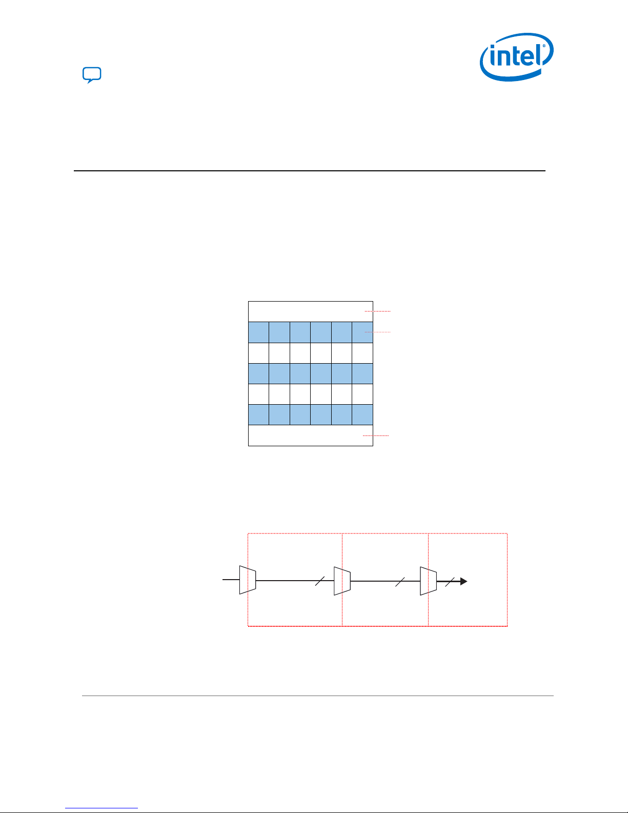
Each Intel Agilex device is divided into a number of evenly sized clock sectors.
Figure 1. Clock Sector Floorplan for Intel Agilex Devices
This figure shows an example of the clock sectors in an Intel Agilex device, which is implemented as an array
of sectors—5 rows and 6 columns in this example. I/O banks are at the top and bottom of the Intel Agilex
device.
2.1.1.1. Clock Network Hierarchy
The Intel Agilex clock network is organized in a hierarchy with 3 levels.
Figure 2. Clock Network Hierarchy
Intel Corporation. All rights reserved. Agilex, Altera, Arria, Cyclone, Enpirion, Intel, the Intel logo, MAX, Nios,
Quartus and Stratix words and logos are trademarks of Intel Corporation or its subsidiaries in the U.S. and/or
other countries. Intel warrants performance of its FPGA and semiconductor products to current specifications in
accordance with Intel's standard warranty, but reserves the right to make changes to any products and services
at any time without notice. Intel assumes no responsibility or liability arising out of the application or use of any
information, product, or service described herein except as expressly agreed to in writing by Intel. Intel
customers are advised to obtain the latest version of device specifications before relying on any published
information and before placing orders for products or services.
*Other names and brands may be claimed as the property of others.
ISO
9001:2015
Registered
Page 5
3232
32
6
32
32
32
32
32
32
32
32
Clock Switch
Multiplexers
Row Clock
(Covers Each Core
Logic Row in Sector)
SCLK
Clock Tap
Multiplexers
Horizontal Clock
Vertical Clock
32
32
32
32
2. Intel Agilex Clocking and PLL Architecture and Features
UG-20216 | 2019.04.02
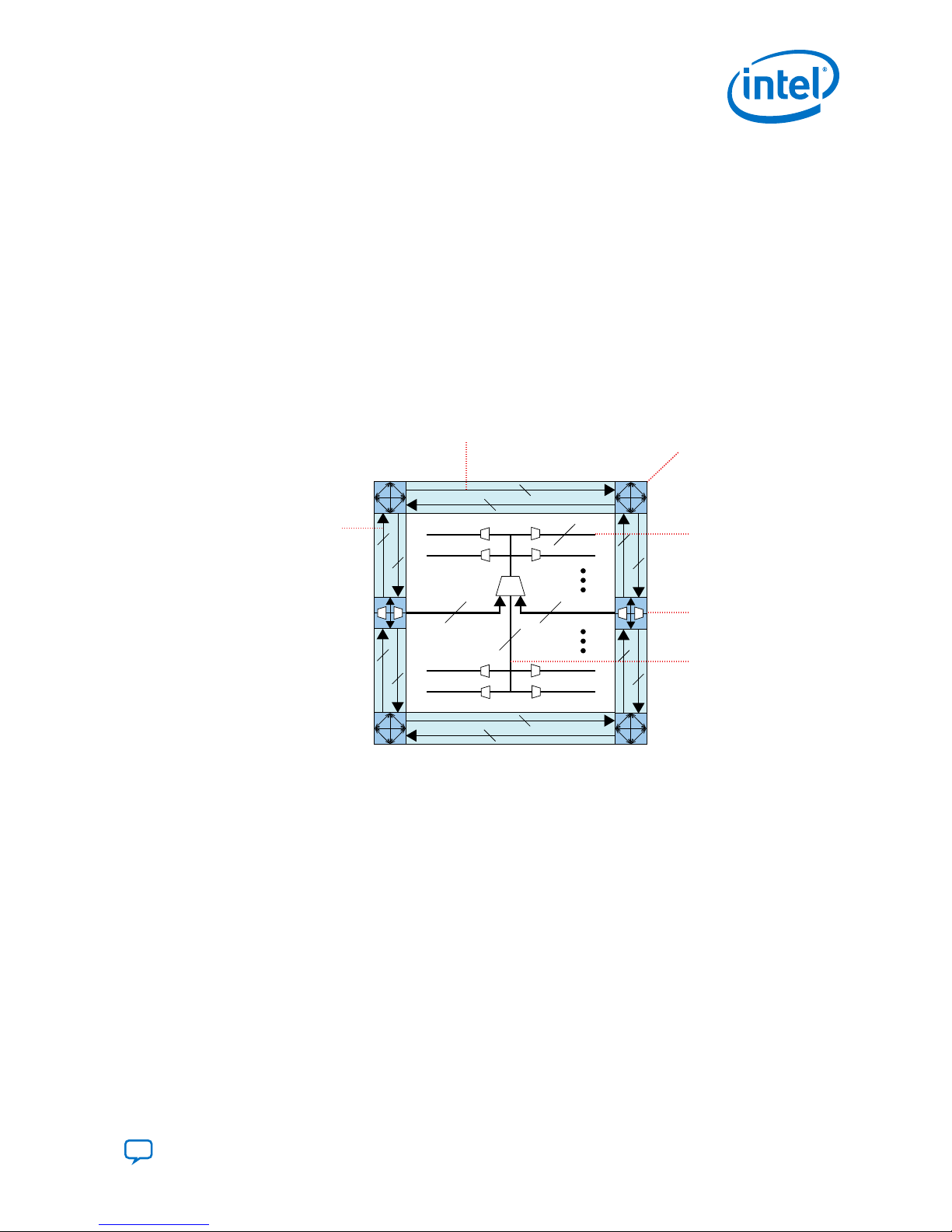
2.1.1.2. Clock Sector
Each clock sector has dedicated sector clock (SCLK) network and row clock network
that can be accessed by the programmable clock routing. On each side of the clock
sector, there is a channel that contains 64 unidirectional wires in bidirectional pairs,
where only one wire in each pair can be used at one time. At each corner, there is a
set of programmable clock switch multiplexer that can route between these clock
wires.
A signal on a vertical clock wire can enter the sector to its left or right via clock tap
multiplexers. The clock tap multiplexer drives a sector clock, which distributes the
signal to each row in the clock sector. In each row, there are six row clock resources
that route to all core functional blocks, PLLs, and I/O interfaces in the sector, and to
adjacent transceivers.
Figure 3. Dedicated Clock Resources Within a Clock Sector
2.1.1.3. Programmable Clock Routing
The Intel Quartus® Prime software automatically configures the clock switch
multiplexer, clock tap multiplexer, SCLK multiplexer, and row clock multiplexers to
generate skew-balanced clock trees. The resulting routing path distributes the signal
from the clock source to all target destinations in one or more clock sectors.
The Intel Quartus Prime software creates efficiently balanced clock tress of various
sizes, ranging from a single clock sector to the entire device, as shown in the following
figure. By default, the Intel Quartus Prime software automatically determines the size
and location of the clock tree. Alternatively, you can directly constrain the clock tree
size and location by using either a Clock Region Assignment or Logic Lock Regions.
The total insertion delay for the clock network depends on the number of clock
resources needed to implement the clock tree, increasing with the number of clock
sectors reached and the distance of the furthest clock destination from the clock
source. As delay increases, the worst-case skew for crossing clock sectors using
different clock tree branches grows, potentially degrading the maximum performance.
For very high-speed clock sources, it is advantageous to reduce the number of clock
Send Feedback
Intel® Agilex™ Clocking and PLL User Guide
5
Page 6
2. Intel Agilex Clocking and PLL Architecture and Features
UG-20216 | 2019.04.02
sectors driven, which reduces the clock skew, and to reduce the distance between the
clock source and the furthest destination, which reduces both clock skew and total
clock insertion delay.
2.1.2. Clock Resources
Table 1. Programmable Clock Routing Resources for Intel Agilex Devices
Number of Resources Available Source of Clock Resource
For transceiver bank:
• Physical medium attachment (PMA) and physical coding sublayer
(PCS) TX and RX clocks per channel
• PMA and PCS TX and RX divide clocks per channel
• Hard IP core clock output signals
•
64 unidirectional programmable clock routing
at the boundary of each clock sector
REFCLK pins
• Core signals
For I/O bank:
•
I/O PLL C counter outputs
•
I/O PLL M counter outputs for feedback
• Phase aligner counter outputs
• Dynamic phase alignment (DPA) clock output
• Clock input pins
• Core signals
(1)
(1)
For more information about the clock input pins connections, refer to the pin
connection guidelines.
Related Information
Intel Agilex Device Family Pin Connection Guidelines
2.1.3. Clock Control Features
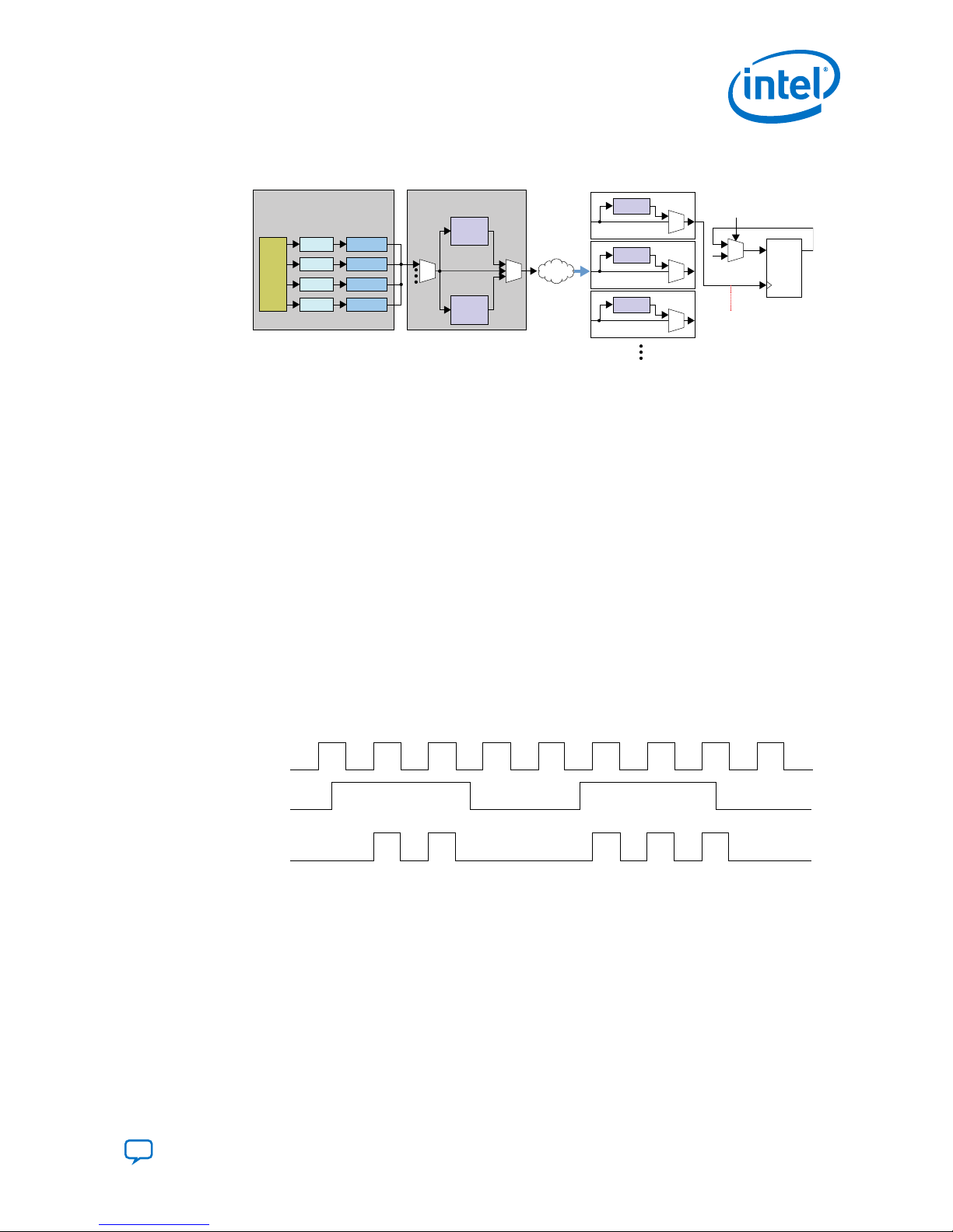
The following figure shows the high level description of the Intel Agilex clock control
features—clock gating and clock divider. The clock from the I/O PLL output can be
gated dynamically. These clock signals along with other clock sources go to the
periphery distributed clock multiplexer (DCM). In the periphery DCM, the clock signal
can either pass straight through, be gated by the root clock gate, or be divided by the
clock divider.
The Intel Quartus Prime software routes the clock signal on the programmable clock
routing to reach each clock sector. The clock signal can be gated in each sector by the
SCLK gates. The clock enters the SCLK network followed by the row clock network,
and eventually reaches the registers in the core. The LAB registers have a built-in
functional clock enable feature, as shown in the following figure.
(1)
Core signals drive directly to programmable clock routing through clock switch multiplexers in
the clock sector instead of the periphery DCM block.
Intel® Agilex™ Clocking and PLL User Guide
6
Send Feedback
Page 7
C Counters
I/O PLL Clock
Gates
I/O
PLL
LAB Level
Gating Signal
D Q
I/O Bank Periphery DCM Block
SCLK
Root Clock
Gate
Programmable
Clock Routing
Clock Gate
Clock Gate
Clock Gate
Clock
Divider
Row Clock
clkena
outclk
inclk
2. Intel Agilex Clocking and PLL Architecture and Features
UG-20216 | 2019.04.02
Figure 4. Clock Gating and Clock Divider in Intel Agilex Clock Network
2.1.3.1. Clock Gating
2.1.3.1.1. Root Clock Gate
There is one root clock gate per I/O bank and transceiver bank. This gate is a part of
the periphery DCM.
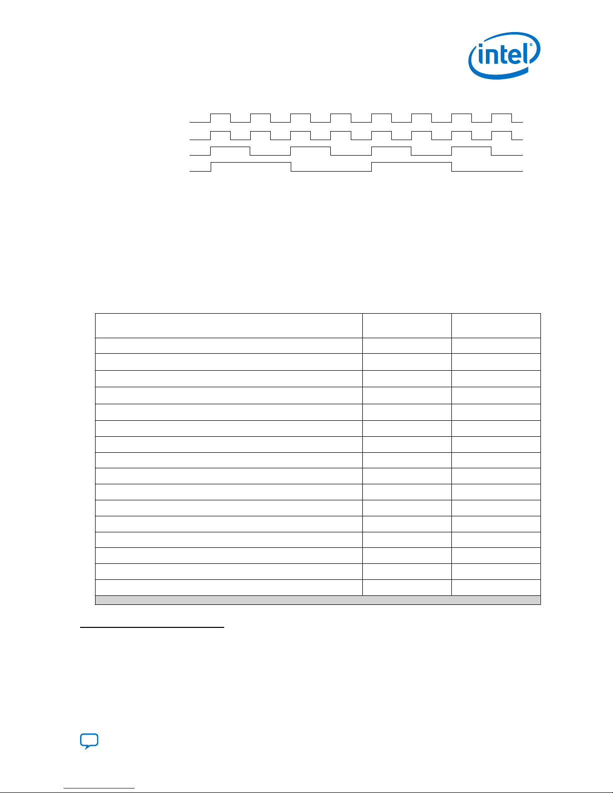
2.1.3.1.2. Sector Clock Gate
Every sector of the device has 32 SCLKs. Each SCLK has a clock gate and bypassable
clock gate path. The SCLK gates are controlled by clock enable inputs from the core
logic. The Intel Quartus Prime software can route up to eight unique clock enable
signals to the 32 SCLKs in a sector.
Intel recommends using the clock gate with a negative latch to provide glitch free
gating on the output clock signal (outclk). The clock gate captures the enable signal
(clkena) on the next rising edge of the input clock signal (inclk). The following
timing diagram shows the relationship of the outclk with respect to inclk and
clkena.
Figure 5. Clock Gating Timing Diagram
The clock signal going into the SCLK network in a sector can only reach the core logic
in that sector. When you instantiate a SCLK gate in your design, the Intel Quartus
Prime software automatically duplicates the SCLK gate to create a clock gate in every
sector to which the clock signal is routed.
The SCLK gate is suitable for cycle-specific clock gating for high-frequency clocks. The
timing of the enable path to the SCLK gate is analyzed by the Intel Quartus Prime
software.
Send Feedback
Intel® Agilex™ Clocking and PLL User Guide
7
Page 8

Related Information
• Clock Sector on page 5
Provides a diagram that shows the dedicated clock resources within a clock
sector.
• Clock Control Features on page 6
Provides a diagram that shows the resources within a SCLK.
2.1.3.1.3. I/O PLL Clock Gate
You can dynamically gate each output counter of the Intel Agilex I/O PLL. This I/O PLL
clock gate provides a useful alternative to the root clock gate. The root clock gate can
gate only 1 of 7 output counters.
However, the I/O PLL clock gate is not cycle-specific. When you use the I/O PLL clock
gate, expect a delay of several clock cycles between the assertion or deassertion of
the clock gate and the corresponding change to the clock signal. The number of delay
cycles is non-deterministic because the enable signal must be synchronized into the
clock domain of the output clock, ensuring a glitch-free gate.
2.1.3.1.4. LAB Clock Gate
The Intel Agilex LAB register has built-in clock gating functionality. The register clock
enable mechanism is a hardened data feedback, as shown in the Clock Gating and
Clock Divider in Intel Agilex Clock Network diagram. The LAB clock gate offers no
associated power savings because this is a purely functional clock enable.
2. Intel Agilex Clocking and PLL Architecture and Features
UG-20216 | 2019.04.02
The analysis and synthesis phases of the Intel Quartus Prime software infer a LAB
clock gate from a behavioral description of clock gating in the register transfer level
(RTL). If a physical clock gate is desired, you must instantiate it explicitly.
Related Information
Clock Control Features on page 6
Provides the Clock Gating and Clock Divider in Intel Agilex Clock Network diagram.
2.1.3.2. Clock Divider
There is one clock divider per I/O bank and transceiver bank. The clock divider is a
part of the periphery DCM block and is located close to the root clock gate. The
outputs of the clock divider cannot be gated by the root clock gate in the same
periphery DCM block. However, this limitation does not apply to the SCLK gate. The
clock divider output in the periphery DCM block can drive a SCLK gate after going
through the programmable clock routing.
The clock divider has three outputs as follows:
• First output—passes through the input clock.
• Second output—divides the input clock by two.
• Third output—divides the input clock by four.
These three clock outputs are edge-aligned at the output of the clock divider.
Intel® Agilex™ Clocking and PLL User Guide
8
Send Feedback
Page 9
clk_div4
clk_div2
clk_div1
inclk
2. Intel Agilex Clocking and PLL Architecture and Features
UG-20216 | 2019.04.02
Figure 6. Clock Divider Timing Diagram
Related Information
Clock Control Features on page 6
Provides a diagram that shows the root clock gate and clock divider in the
periphery DCM block.
2.2. PLLs Architecture and Features
2.2.1. PLL Features
Table 2. PLL Features in Intel Agilex Devices—Preliminary
Feature I/O Bank I/O PLL Fabric-Feeding I/O
Integer PLL Yes Yes
Number of C output counter
M counter divide factor range
N counter divide factor range
C counter divide factor range
Dedicated external clock outputs Yes Yes
Dedicated clock input pins Yes Yes
External feedback input pin Yes Yes
Source synchronous compensation
Direct compensation Yes Yes
Normal compensation
Zero-delay buffer compensation Yes Yes
External feedback compensation Yes Yes
LVDS compensation Yes —
Voltage-controlled oscillator (VCO) output drives the DPA clock Yes —
Phase shift resolution
(2)
(3)
(2)
7 3
4 to 160 4 to 160
1 to 110 1 to 110
1 to 510 1 to 510
Yes Yes
Yes Yes
78.125 ps 78.125 ps
PLL
continued...
(2)
Non-dedicated feedback path option is available for this compensation mode.
(3)
The smallest phase shift is determined by the VCO period divided by eight. For degree
increments, the Intel Agilex device can shift all output frequencies in increments of at least
45°. Smaller degree increments are possible depending on the frequency and divide
parameters.
Send Feedback
Intel® Agilex™ Clocking and PLL User Guide
9
Page 10

General-Purpose I/O Bank
I/O Bank
I/O PLL
Sub Bank
Fabric-Feeding
I/O PLL
I/O Bank
I/O PLL
Sub Bank
2. Intel Agilex Clocking and PLL Architecture and Features
UG-20216 | 2019.04.02
Feature I/O Bank I/O PLL Fabric-Feeding I/O
Programmable duty cycle Yes Yes
Power down mode Yes Yes
Bandwidth setting Low, medium, and
high
2.2.2. PLL Usage
I/O PLLs are optimized for use with memory interfaces and LVDS SERDES. You can
use the I/O PLLs to:
• Reduce the number of required oscillators on the board
• Reduce the clock pins used in the FPGA by synthesizing multiple clock frequencies
from a single reference clock source
• Simplify the design of external memory interfaces and high-speed LVDS interfaces
• Ease timing closure because the I/O PLLs are tightly coupled with the I/Os
• Compensate for clock network delay
• Zero delay buffering
2.2.3. PLL Locations
Figure 7. I/O PLL Locations in I/O Bank
PLL
Medium and high
Intel® Agilex™ Clocking and PLL User Guide
10
Send Feedback
Page 11

÷C1
÷C2
÷C3
÷C6
÷C0
÷M
PLL Output Multiplexer
Cascade Output to
Adjacent I/O PLL
LVDS RX/TX Clock
Programmable clock routing
FBOUT
FBIN
LVDS Clock Network
Dedicated clock inputs
from the same I/O bank
Programmable clock routing
cascade input from I/O PLL
in the same I/O column
or dedicated clock Inputs
from other I/O bank in the
same I/O column
4
8
8
To DPA Block
Direct Compensation Mode
Zero Delay Buffer, External Feedback Modes
LVDS Compensation Mode
extswitch
clkbad0
clkbad1
activeclock
Lock
Circuit
For single-ended clock inputs, only the CLKp and CLKn pins
have dedicated connection to the PLL.
This FBOUT port is fed by
the M counter in the PLLs.
LVDS RX/TX Load Enable
External Memory Interface DLL
Programmable Clock Routing
Source Synchronous, Normal Modes
You can choose non-dedicated feedback path option
for these compensation modes.
÷N
Clock
Switchover
Block
inclk0
inclk1
PFD CP LF VCO
locked
÷C1
÷C2
÷C0
÷M
PLL Output Multiplexer
Programmable clock routing
FBOUT
FBIN
Dedicated clock inputs
from the same I/O bank
Dedicated clock inputs from the
same I/O banks, or inputs from
other I/O banks in the same
I/O column or PLLs routed
over the global clock network
4
8
Direct Compensation Mode
Zero Delay Buffer, External Feedback Modes
extswitch
clkbad0
clkbad1
activeclock
Lock
Circuit
For single-ended clock inputs, only the CLKp and CLKn pins
have dedicated connection to the PLL.
This FBOUT port is fed by
the M counter in the PLLs.
Programmable Clock Routing
Source Synchronous, Normal Modes
You can choose non-dedicated feedback path option
for these compensation modes.
÷N
Clock
Switchover
Block
inclk0
inclk1
PFD CP LF VCO
locked
2. Intel Agilex Clocking and PLL Architecture and Features
UG-20216 | 2019.04.02
2.2.4. PLL Architecture
Figure 8. I/O Bank I/O PLL High-Level Block Diagram for Intel Agilex Devices
Figure 9. Fabric-Feeding I/O PLL High-Level Block Diagram for Intel Agilex Devices
2.2.5. PLL Control Signals
You can use the reset signal to control PLL operation and resynchronization, and use
the locked signal to observe the status of the PLL.
2.2.5.1. Reset
The reset signal port of the IP core for I/O PLL is reset.
The reset signal is the reset or resynchronization input for each I/O PLL. The device
input pins or internal logic can drive these input signals.
When the reset signal is driven high, the I/O PLL counters reset, clearing the I/O PLL
output and placing the I/O PLL out-of-lock. The VCO is then set back to its nominal
Send Feedback
setting. When the reset signal is driven low again, the I/O PLL resynchronizes to its
input clock source as it re-locks.
Intel® Agilex™ Clocking and PLL User Guide
11
Page 12

2. Intel Agilex Clocking and PLL Architecture and Features
UG-20216 | 2019.04.02
You must assert the reset signal every time the I/O PLL loses lock to guarantee the
correct phase relationship between the I/O PLL input and output clocks. You can set
up the I/O PLL to automatically reset (self-reset) after a loss-of-lock condition using
the Intel Quartus Prime parameter editor.
You must include the reset signal if either of the following conditions is true:
• I/O PLL reconfiguration or clock switchover is enabled in the design.
• Phase relationships between the I/O PLL input and output clocks must be
maintained after a loss-of-lock condition.
Note: Reset the I/O PLL after the input clock is stable and within specifications, even when
the self-reset feature is enabled, if either one of the following conditions occur:
• The input clock to the I/O PLL is not toggling or is unstable when the FPGA
transitions into user mode.
• The I/O PLL cannot lock to the reference clock after reconfiguring the I/O PLL.
Related Information
PLL Calibration on page 24
2.2.5.2. Locked
The locked signal port of the IP core for the I/O PLL is locked.
The lock detection circuit provides a signal to the core logic. The signal indicates when
the feedback clock locks onto the reference clock both in phase and frequency.
When PLL loses lock, the output of the PLL starts drifting out of the desired frequency.
The downstream logic must be held inactive when PLL has lost lock.
2.2.6. PLL Feedback Modes
PLL feedback modes compensate for clock network delays to align the rising edge of
the output clock with the rising edge of the PLL's reference clock. Select the
appropriate type of compensation for the timing critical clock path in your design.
PLL compensation is not always needed. A PLL should be configured in direct (no
compensation) mode unless a need for compensation is identified. Direct mode
provides the best PLL jitter performance and avoids expending compensation clocking
resources unnecessarily.
The default PLL feedback mode is direct compensation mode.
I/O PLLs support the following PLL feedback modes:
• Direct compensation
• LVDS compensation
• Source synchronous compensation
• Normal compensation
• Zero delay buffer (ZDB) compensation
• External feedback (EFB) compensation
Intel® Agilex™ Clocking and PLL User Guide
12
Send Feedback
Page 13

PLL Reference
Clock at the
Input Pin
PLL Clock at the
Register Clock Port
External PLL
Clock Outputs
Phase Aligned
The PLL clock outputs lag
the PLL input clocks
depending on routing
delays.
2. Intel Agilex Clocking and PLL Architecture and Features
UG-20216 | 2019.04.02
Normal and source synchronous compensation modes compensate for the insertion
delay of a routed core clock. For Intel Agilex devices, you can achieve core clock
compensation by routing a dedicated feedback clock from the M counter in the I/O PLL
to emulate the insertion delay of the compensated C counter output clock network.
Intel recommends the non-dedicated feedback mechanism because it uses the clock
resources most efficiently.
2.2.6.1. Direct Compensation Mode
In direct mode, the PLL does not compensate for any clock network delays. This mode
provides better jitter performance compared to other compensation modes because
the clock feedback into the phase frequency detector (PFD) passes through less
circuitry. Both the PLL internal- and external-clock outputs are phase-shifted with
respect to the PLL clock input.
Figure 10. Example of Phase Relationship Between the PLL Clocks in Direct Mode
2.2.6.2. LVDS Compensation Mode
LVDS compensation mode maintains the same data and clock timing relationship seen
at the pins of the internal serializer/deserializer (SERDES) capture register, except that
the clock is inverted (180° phase shift). Thus, LVDS compensation mode ideally
compensates for the delay of the LVDS clock network, including the difference in delay
between the following two paths:
• Data pin-to-SERDES capture register
• Clock input pin-to-SERDES capture register
The output counter must provide the 180° phase shift.
Send Feedback
Intel® Agilex™ Clocking and PLL User Guide
13
Page 14

Data Pin
Data at the Register
Clock at the Register
PLL Reference Clock
at the Input Pin
Data Pin
PLL Reference Clock
at the Input Pin
Data at the Register
Clock at the Register
2. Intel Agilex Clocking and PLL Architecture and Features
UG-20216 | 2019.04.02
Figure 11. Example of Phase Relationship Between the Clock and Data in LVDS
Compensation Mode
2.2.6.3. Source Synchronous Compensation Mode
If the data and clock signals arrive at the same time on the input pins, the same
phase relationship is maintained at the clock and data ports of any IOE input register.
Data and clock signals at the IOE experience similar buffer delays as long as you use
the same I/O standard. Only one output clock can be compensated in source
synchronous compensation mode.
Intel recommends source synchronous mode for source synchronous data transfers.
Figure 12. Example of Phase Relationship Between Clock and Data in Source
Synchronous Mode
The source synchronous mode compensates for the delay of the clock network used
and any difference in the delay between the following two paths:
• Data pin to the IOE register input
• Clock input pin to the PLL PFD input
The Intel Agilex PLL can compensate multiple pad-to-input-register paths, such as a
data bus when it is set to use source synchronous compensation mode.
Intel® Agilex™ Clocking and PLL User Guide
14
Send Feedback
Page 15

PLL Clock at the
Register Clock Port
Dedicated PLL
Clock Outputs
Phase Aligned
PLL Reference
Clock at the Input Pin
The external clock output can
lead or lag the PLL internal
clock signals.
2. Intel Agilex Clocking and PLL Architecture and Features
UG-20216 | 2019.04.02
2.2.6.4. Normal Compensation Mode
An internal clock in normal compensation mode is phase-aligned to the input clock pin.
The external clock output pin has a phase delay relative to the clock input pin if
connected in this mode. The Intel Quartus Prime Timing Analyzer reports any phase
difference between the two. In normal compensation mode, the delay introduced by
the clock network is fully compensated. Only one output clock can be compensated in
normal compensation mode.
Figure 13. Example of Phase Relationship Between the PLL Clocks in Normal
Compensation Mode
2.2.6.5. Zero-Delay Buffer Mode
In zero-delay buffer (ZDB) mode, the external clock output pin is phase-aligned with
the clock input pin for zero delay through the device.
In this mode, you must use the same I/O standard on the input clocks and clock
outputs to guarantee clock alignment at the input and output pins. You cannot use
differential I/O standards on the PLL clock input or output pins.
To ensure phase alignment between the clk pin and the external clock output
(CLKOUT) pin in ZDB mode, instantiate a bidirectional I/O pin in the design. The
bidirectional I/O pin serves as the feedback path connecting the fbout and fbin
ports of the PLL. The bidirectional I/O pin must always be assigned a single-ended I/O
standard. The PLL uses this bidirectional I/O pin to mimic and compensate for the
output delay from the clock output port of the PLL to the external clock output pin.
bidirectional I/O pin.
Note: To avoid signal reflection when using ZDB mode, do not place board traces on the
Send Feedback
Intel® Agilex™ Clocking and PLL User Guide
15
Page 16

PLL Clock at the
Register Clock Port
Dedicated PLL
Clock Outputs
Phase Aligned
PLL Reference
Clock at the Input Pin
The internal PLL clock
output can lead or lag
the external PLL clock
outputs.
2. Intel Agilex Clocking and PLL Architecture and Features
UG-20216 | 2019.04.02
Figure 14. Example of Phase Relationship Between the PLL Clocks in ZDB Mode
2.2.6.6. External Feedback Mode
In external feedback (EFB) mode, the output of the M counter (fbout) feeds back to
the PLL fbin input (using a trace on the board) and becomes part of the feedback
loop.
One of the dual-purpose external clock outputs becomes the fbin input pin in this
mode. The external feedback input pin, fbin is phase-aligned with the clock input pin.
Aligning these clocks allows you to remove clock delay and skew between devices.
In EFB mode, you must use the same I/O standard on the input clock, feedback input,
and clock outputs.
Intel® Agilex™ Clocking and PLL User Guide
16
Send Feedback
Page 17

Dedicated PLL
Clock Outputs
PLL Clock at
the Register
Clock Port
fbin Clock Input Pin
Phase Aligned
PLL Reference
Clock at the
Input Pin
The PLL clock outputs
can lead or lag the fbin
clock input.
2. Intel Agilex Clocking and PLL Architecture and Features
UG-20216 | 2019.04.02
Figure 15. Example of Phase Relationship Between the PLL Clocks in EFB Mode
2.2.7. Clock Multiplication and Division
An Intel Agilex PLL output frequency is related to its input reference clock source by
the scale factor: M/(N × C) for I/O PLL.
The input clock is divided by a pre-scale factor, N, and is then multiplied by the M
feedback factor. The control loop drives the VCO to match f
non-dedicated feedback path in normal or source synchronous compensation mode,
the control loop drives the VCO to match f
compensated outclk C counter value. The Intel Quartus Prime software automatically
chooses the appropriate scale factors according to the input frequency, multiplication,
and division values entered into the Intel FPGA IP cores for I/O PLL.
Pre-Scale Counter, N and Multiply Counter, M
Each PLL has one pre-scale counter, N, and one multiply counter, M. The M and N
counters do not use duty-cycle control because the only purpose of these counters is
to calculate frequency division.
Post-Scale Counter, C
Each output port has a unique post-scale counter, C. For multiple C counter outputs
with different frequencies, the VCO is set to the least common multiple of the output
frequencies that meets its frequency specifications. For example, if the output
frequencies required from one I/O PLL are 55 MHz and 100 MHz, the Intel Quartus
× (M/N). When using
in
× ((M × Ci)/N), where C
in
is the
i
Send Feedback
Intel® Agilex™ Clocking and PLL User Guide
17
Page 18

Prime software sets the VCO frequency to 1.1 GHz (the least common multiple of
55 MHz and 100 MHz within the VCO operating frequency range). Then the post-scale
counters, C, scale down the VCO frequency for each output port.
Integer Mode
The I/O PLL can only operate in integer mode.
2.2.8. Programmable Phase Shift
The programmable phase shift feature allows only the I/O PLLs to generate output
clocks with a fixed phase offset.
The VCO frequency of the PLL determines the precision of the phase shift. The
minimum phase shift increment is 1/8 of the VCO period. For example, if an I/O PLL
operates with a VCO frequency of 1000 MHz, phase shift steps of 125 ps are possible.
The Intel Quartus Prime software automatically adjusts the VCO frequency according
to the user-specified phase shift values entered into the IP core.
2.2.9. Programmable Duty Cycle
The programmable duty cycle feature allows I/O PLLs to generate clock outputs with a
variable duty cycle. This feature is only supported by the I/O PLL post-scale counters,
C.
2. Intel Agilex Clocking and PLL Architecture and Features
UG-20216 | 2019.04.02
The I/O PLL C counter value determines the precision of the duty cycle. The precision
is 50% divided by the post-scale counter value. For example, if the C0 counter is 10,
steps of 5% are possible for duty-cycle options from 5% to 90%. If the I/O PLL is in
external feedback mode, set the duty cycle for the counter driving the fbin pin to
50%.
The Intel Quartus Prime software automatically adjusts the VCO frequency according
to the required duty cycle that you enter in the IP core.
Combining the programmable duty cycle with programmable phase shift allows the
generation of precise non-overlapping clocks.
2.2.10. PLL Cascading
Intel Agilex devices support PLL-to-PLL cascading. You can cascade a maximum of two
PLLs. PLL cascading synthesizes more output clock frequencies than a single PLL.
If you cascade PLLs in your design, the source (upstream) PLL must have a lowbandwidth setting, and the destination (downstream) PLL must have a high-bandwidth
setting for I/O PLL. During cascading, the output of the source PLL serves as the
reference clock (input) of the destination PLL. The bandwidth settings of cascaded
PLLs must be different. If the bandwidth settings of the cascaded PLLs are the same,
the cascaded PLLs may amplify phase noise at certain frequencies.
Intel® Agilex™ Clocking and PLL User Guide
18
Send Feedback
Page 19

UPSTREAM_IOPLL
refclk cascade_out
locked
outclk[8:0]
reset
DOWNSTREAM_IOPLL
adjpllin
locked
outclk[8:0]
permit_cal
reset
UPSTREAM_IOPLL
refclk
locked
outclk[0] (1)
reset
DOWNSTREAM_IOPLL
permit_cal
locked
outclk[8:0]
refclk
reset
Note:
(1) You may connect any of the outclk from the upstream I/O PLL to the refclk port in the downstream I/O PLL when cascading the I/O PLL via
core clock fabric.
2. Intel Agilex Clocking and PLL Architecture and Features
UG-20216 | 2019.04.02
Intel Agilex devices support the following PLL-to-PLL cascading modes for I/O bank I/O
PLL:
• I/O-PLL-to-I/O-PLL cascading via dedicated cascade path—upstream I/O PLL and
downstream I/O PLL must be in the same I/O column.
• I/O-PLL-to-I/O-PLL cascading via core clock fabric—no restriction on locations of
upstream and downstream I/O PLL.
The permit_cal input of the downstream I/O PLL must be connected to the locked
output of the upstream I/O PLL in both PLL cascading modes.
The following figures show the connectivity required between the upstream and
downstream I/O PLL for both the PLL cascading modes.
Figure 16. I/O-PLL-to-I/O-PLL Cascading Via Dedicated Cascade Path
Figure 17. I/O-PLL-to-I/O-PLL Cascading Via Core Clock Fabric
2.2.11. PLL Input Clock Switchover
The clock switchover feature allows the I/O PLL to switch between two reference input
clocks. Use this feature for clock redundancy or for a dual-clock domain application
where a system turns to the redundant clock if the previous clock stops running. The
design can perform clock switchover automatically when the clock is no longer
toggling or based on a user control signal, extswitch.
Send Feedback
Intel® Agilex™ Clocking and PLL User Guide
19
Page 20

Clock
Sense
Switchover
State Machine
Clock Switch
Control Logic
N Counter
inclk0
inclk1
Multiplexer
Out
clkbad0
clkbad1
activeclock
extswitch
refclk
fbclk
clksw
PFD
2. Intel Agilex Clocking and PLL Architecture and Features
Intel Agilex I/O PLLs support the following clock switchover modes:
• Automatic switchover—the clock sense circuit monitors the current reference
clock. If the current reference clock stops toggling, the reference clock
automatically switches to inclk0 or inclk1 clock.
•
Manual clock switchover—clock switchover is controlled using the extswitch
signal. When the extswitch signal goes from logic high to logic low, and stays
low for at least three clock cycles for the inclk being switched to, the reference
clock to the I/O PLL is switched from inclk0 to inclk1, or vice-versa.
• Automatic switchover with manual override—this mode combines automatic
switchover and manual clock switchover. When the extswitch signal goes low, it
overrides the automatic clock switchover function. As long as the extswitch
signal is low, further switchover action is blocked.
2.2.11.1. Automatic Switchover
Intel Agilex I/O PLLs support a fully configurable clock switchover capability.
Figure 18. Automatic Clock Switchover Circuit Block Diagram
This figure shows a block diagram of the automatic switchover circuit built into the I/O PLL.
UG-20216 | 2019.04.02
When the current reference clock is not present, the clock sense block automatically
switches to the backup clock for I/O PLL reference. You can select a clock source as
the backup clock by connecting it to the inclk1 port of the I/O PLL in your design.
The clock switchover circuit sends out three status signals—clkbad0, clkbad1, and
activeclock—from the I/O PLL to implement a custom switchover circuit in the logic
array.
In automatic switchover mode, the clkbad0 and clkbad1 signals indicate the status
of the two clock inputs. When they are asserted, the clock sense block detects that the
corresponding clock input has stopped toggling. These two signals are not valid if the
frequency difference between inclk0 and inclk1 is greater than 20%.
Intel® Agilex™ Clocking and PLL User Guide
20
Send Feedback
Page 21

2. Intel Agilex Clocking and PLL Architecture and Features
UG-20216 | 2019.04.02
The activeclock signal indicates which of the two clock inputs (inclk0 or inclk1)
is being selected as the reference clock to the I/O PLL. When the frequency difference
between the two clock inputs is more than 20%, the activeclock signal is the only
valid status signal.
Use the switchover circuitry to automatically switch between inclk0 and inclk1
when the current reference clock to the I/O PLL stops toggling. You can switch back
and forth between inclk0 and inclk1 any number of times when one of the two
clocks fails and the other clock is available.
For example, in applications that require a redundant clock with the same frequency
as the reference clock, the switchover state machine generates a signal (clksw) that
controls the multiplexer select input. In this case, inclk1 becomes the reference
clock for the I/O PLL.
When using automatic clock switchover mode, the following requirements must be
satisfied:
• Both clock inputs must be running when the FPGA is configured.
• The period of the two clock inputs can differ by no more than 20%.
• The input clocks must meet the input jitter specifications and I/O standard
specifications.
Glitches in the input clock may be seen as a greater than 20% difference in frequency
between the input clocks.
If the current clock input stops toggling while the other clock is also not toggling,
switchover is not initiated and the clkbad[0..1] signals are not valid. If both clock
inputs are not the same frequency, but their period difference is within 20%, the clock
sense block detects when a clock stops toggling. However, the I/O PLL may lose lock
after the switchover is completed and needs time to relock.
Note: You must reset the I/O PLL using the reset signal to maintain the phase relationships
between the I/O PLL input and output clocks when using clock switchover.
Send Feedback
Intel® Agilex™ Clocking and PLL User Guide
21
Page 22

inclk0
inclk1
muxout
clkbad0
clkbad1
activeclock
Switchover is enabled on the falling
edge of inclk0 or inclk1, depending on
which clock is available. In this figure,
switchover is enabled on the falling
edge of inclk1.
2. Intel Agilex Clocking and PLL Architecture and Features
Figure 19. Automatic Switchover After Loss of Clock Detection
This figure shows an example waveform of the switchover feature in automatic switchover mode. In this
example, the inclk0 signal is held low. After the inclk0 signal is held low for approximately two clock cycles,
the clock sense circuitry drives the clkbad0 signal high. As the reference clock signal (inclk0) is not
toggling, the switchover state machine controls the multiplexer through the extswitch signal to switch to the
backup clock, inclk1.
UG-20216 | 2019.04.02
2.2.11.2. Automatic Switchover with Manual Override
In automatic switchover with manual override mode, you can use the extswitch
signal for user- or system-controlled switch conditions. You can use this mode for
same-frequency switchover, or to switch between inputs of different frequencies.
For example, if inclk0 is 66 MHz and inclk1 is 200 MHz, you must control
switchover using the extswitch signal. The automatic clock-sense circuitry cannot
monitor clock input (inclk0 and inclk1) frequencies with a frequency difference of
more than 100% (2×).
This feature is useful when the clock sources originate from multiple cards on the
backplane, requiring a system-controlled switchover between the frequencies of
operation.
You must choose the backup clock frequency and set the M, N, and C counters so that
the VCO operates within the recommended operating frequency range. The Intel
Quartus Prime software notifies you if a given combination of inclk0 and inclk1
frequencies cannot meet this requirement.
Intel® Agilex™ Clocking and PLL User Guide
22
Send Feedback
Page 23

inclk0
inclk1
muxout
clkbad0
clkbad1
activeclock
extswitch
To initiate a manual clock switchover event,
both inclk0 and inclk1 must be running when
the extswitch signal goes low.
2. Intel Agilex Clocking and PLL Architecture and Features
UG-20216 | 2019.04.02
Figure 20.
Clock Switchover Using the extswitch (Manual) Control
This figure shows a clock switchover waveform controlled by the extswitch signal. In this case, both clock
sources are functional and inclk0 is selected as the reference clock. The switchover sequence starts when the
extswitch signal goes low. On the falling edge of inclk0, the counter’s reference clock, muxout, is gated off
to prevent clock glitching. On the falling edge of inclk1, the reference clock multiplexer switches from
inclk0 to inclk1 as the I/O PLL reference. The activeclock signal changes to indicate the clock which is
currently feeding the I/O PLL.
In automatic override with manual switchover mode, the activeclock signal inverts
after the extswitch signal transitions from logic high to logic low. Since both clocks
are still functional during the manual switch, neither clkbad signal goes high.
Because the switchover circuit is negative-edge sensitive, the rising edge of the
extswitch signal does not cause the circuit to switch back from inclk1 to inclk0.
When the extswitch signal goes low again, the process repeats.
The extswitch signal and automatic switch work only if the clock being switched to
is available. If the clock is not available, the state machine waits until the clock is
available.
2.2.11.3. Manual Clock Switchover
In manual clock switchover mode, the extswitch signal controls whether inclk0 or
inclk1 is selected as the input clock to the I/O PLL. By default, inclk0 is selected.
A clock switchover event is initiated when the extswitch signal transitions from logic
high to logic low, and is held low for at least three inclk cycles for the inclk clock
being switched to.
You must bring the extswitch signal back high again to perform another switchover
event. If you do not require another switchover event, you can leave the extswitch
signal in a logic low state after the initial switch.
If inclk0 and inclk1 are different frequencies and are always running, the
extswitch signal minimum low time must be greater than or equal to three of the
slower frequency inclk0 and inclk1 cycles.
Send Feedback
Intel® Agilex™ Clocking and PLL User Guide
23
Page 24

Clock Switch
Control Logic
N Counter
PFD
inclk0
inclk1
muxout refclk
fbclk
extswitch
2. Intel Agilex Clocking and PLL Architecture and Features
Figure 21. Manual Clock Switchover Circuitry in Intel Agilex I/O PLLs
You can delay the clock switchover action by specifying the switchover delay in the
Intel FPGA IP cores for the I/O PLL. When you specify the switchover delay, the
extswitch signal must be held low for at least three inclk cycles for the inclk
being switched to plus the number of the delay cycles that you specify to initiate a
clock switchover.
2.2.12. PLL Reconfiguration and Dynamic Phase Shift
Intel Agilex devices support PLL reconfiguration and dynamic phase shift with the
following features:
•
PLL reconfiguration—I/O PLL can reconfigure the M, N, C counters, and bandwidth
setting.
• Dynamic phase shift—I/O PLL can perform positive or negative phase shift. Able to
shift multiple phase steps each time, where one phase step is equal to 1/8 of the
VCO period.
UG-20216 | 2019.04.02
2.2.13. PLL Calibration
I/O PLLs include both analog and digital blocks that require calibration to compensate
for process, voltage, and temperature (PVT) variations. Intel Agilex uses the I/O
manager to perform calibration routines.
There are two main types of calibration.
• Power-up calibration—initiates automatically at device power-up and runs during
device configuration.
• User calibration—if you perform dynamic reconfiguration or change the reference
clock frequency of the I/O PLL, you must perform user recalibration. You must
enable the required calibration sequence.
To successfully complete the calibration process, OSC_CLK_1 clocks and all reference
clocks driving the I/O PLLs must be stable and free running at the start of FPGA
configuration. If clock switchover is enabled, both reference clocks must be present for
calibration. During user mode, when the I/O PLL does not detect a reference clock
during configuration, calibration attempts continue periodically. After calibration has
completed, the I/O PLL is locked automatically.
2.2.13.1. Power-Up Calibration
After device power-up, the I/O manager automatically initiates the calibration process.
The process continues during device programming.
Intel® Agilex™ Clocking and PLL User Guide
24
Send Feedback
Page 25

2. Intel Agilex Clocking and PLL Architecture and Features
UG-20216 | 2019.04.02
2.2.13.2. User Calibration
The I/O PLL must be recalibrated for any of the following conditions after device power
up:
•
Dynamic I/O PLL reconfiguration that changes the M or N counter settings is
performed.
• Change of the reference clock frequency to the I/O PLL.
Recalibration is not necessary when using clock switchover to a secondary reference
clock with a different frequency than the primary reference clock. The I/O PLL stores
the calibration settings for both reference clocks after power-up calibration.
Send Feedback
Intel® Agilex™ Clocking and PLL User Guide
25
Page 26

UG-20216 | 2019.04.02
Send Feedback
3. Intel Agilex Clocking and PLL Design Considerations
3.1. Guideline: Clock Switchover
When implementing clock switchover in Intel Agilex I/O PLLs, refer to the following
guidelines:
•
Automatic clock switchover requires that the inclk0 and inclk1 frequencies are
within 20% of each other. Failing to meet this requirement causes the clkbad0
and clkbad1 signals to not function properly.
•
When using manual clock switchover, the difference between inclk0 and inclk1
can be more than 100% (2×). However, differences in frequency, phase, or both,
of the two clock sources may cause the I/O PLL to lose lock. Resetting the I/O PLL
ensures that you maintain the correct phase relationships between the input and
output clocks.
•
Both inclk0 and inclk1 must be running when the extswitch signal goes low
to initiate the manual clock switchover event. Failing to meet this requirement
causes the clock switchover to not function properly.
• Applications that require a clock switchover feature and a small frequency drift
must use a low-bandwidth I/O PLL. When referencing input clock changes, the
low-bandwidth I/O PLL reacts more slowly than a high-bandwidth I/O PLL. When
switchover happens, a low-bandwidth I/O PLL propagates the stopping of the clock
to the output more slowly than a high-bandwidth I/O PLL. However, the lowbandwidth I/O PLL also increases lock time.
• After a switchover occurs, there may be a finite resynchronization period for the
I/O PLL to lock onto a new clock. The time it takes for the I/O PLL to relock
depends on the I/O PLL configuration.
• If the phase relationship between the input clock to the I/O PLL and the output
clock from the I/O PLL is important in your design, assert the reset signal for at
least 10 ns after performing a clock switchover. Wait for the locked signal to go
high and be stable before re-enabling the output clocks from the I/O PLL.
• The VCO frequency gradually decreases when the current clock is lost and then
increases as the VCO locks on to the backup clock, as shown in the following
figure.
Intel Corporation. All rights reserved. Agilex, Altera, Arria, Cyclone, Enpirion, Intel, the Intel logo, MAX, Nios,
Quartus and Stratix words and logos are trademarks of Intel Corporation or its subsidiaries in the U.S. and/or
other countries. Intel warrants performance of its FPGA and semiconductor products to current specifications in
accordance with Intel's standard warranty, but reserves the right to make changes to any products and services
at any time without notice. Intel assumes no responsibility or liability arising out of the application or use of any
information, product, or service described herein except as expressly agreed to in writing by Intel. Intel
customers are advised to obtain the latest version of device specifications before relying on any published
information and before placing orders for products or services.
*Other names and brands may be claimed as the property of others.
ISO
9001:2015
Registered
Page 27

∆ F
vco
Primary Clock Stops Running
VCO Tracks Secondary Clock
Switchover Occurs
3. Intel Agilex Clocking and PLL Design Considerations
UG-20216 | 2019.04.02
Figure 23. VCO Switchover Operating Frequency
3.2. Guideline: Timing Closure
For timing closure, refer to the following guidelines:
• Reconfiguring a PLL's counter and loop filter settings changes both the output
frequency and the clock uncertainty of that I/O PLL. Dynamic phase shift only
affects the output clock phase.
• The Timing Analyzer in the Intel Quartus Prime software performs timing analysis
for the initial PLL settings only. You must verify that your design closes timing
after dynamic reconfiguration or dynamic phase shift.
• Intel recommends compiling the I/O PLL designs with each intended configuration
setting to determine the variation in the clock with the I/O PLL settings.
Related Information
Creating Clocks and Clock Constraints chapter, Intel Quartus Prime Pro Edition User
Guide: Timing Analyzer
3.3. Guideline: Resetting the PLL
To reset the PLL, refer to the following guidelines:
•
When changing the M counter, N counter, or loop filter settings, the I/O PLL may
lose and regain lock. To maintain the appropriate phase relationship between the
reference clock and output clocks, assert the areset signal to reset the I/O PLL
after reconfiguration is complete. Intel recommends always resetting the I/O PLL
after any reconfiguration operation to the M counter, N counter, or loop filter
settings.
•
When changing the C counter settings, you may lose the expected phase
relationship between the C counters. Assert the areset signal after
reconfiguration is complete to restore the expected phase relationship. Reset is
not required if the phase relationships are not important to your application.
• Resetting the I/O PLL does not modify the counter or loop filter settings. However,
resetting the I/O PLL undoes any dynamic phase shift operations that were
performed. After the I/O PLL is reset, the phase shift on the C counters is restored
to the originally programmed settings.
Send Feedback
Intel® Agilex™ Clocking and PLL User Guide
27
Page 28

3. Intel Agilex Clocking and PLL Design Considerations
3.4. Guideline: Configuration Constraints
The I/O PLL configuration must obey the following constraints:
• The phase frequency detector (PFD) and VCO each have a legal frequency range
of operation.
•
The loop filter settings must be appropriate for the M counter value and userselected bandwidth mode.
If any of these configuration constraints are violated, the I/O PLL may fail to lock or
may exhibit poor jitter performance.
UG-20216 | 2019.04.02
Intel® Agilex™ Clocking and PLL User Guide
28
Send Feedback
Page 29

UG-20216 | 2019.04.02
Send Feedback
4. Document Revision History for the Intel Agilex Clocking
and PLL User Guide
Document
Version
2019.04.02 Initial release.
Changes
Intel Corporation. All rights reserved. Agilex, Altera, Arria, Cyclone, Enpirion, Intel, the Intel logo, MAX, Nios,
Quartus and Stratix words and logos are trademarks of Intel Corporation or its subsidiaries in the U.S. and/or
other countries. Intel warrants performance of its FPGA and semiconductor products to current specifications in
accordance with Intel's standard warranty, but reserves the right to make changes to any products and services
at any time without notice. Intel assumes no responsibility or liability arising out of the application or use of any
information, product, or service described herein except as expressly agreed to in writing by Intel. Intel
customers are advised to obtain the latest version of device specifications before relying on any published
information and before placing orders for products or services.
*Other names and brands may be claimed as the property of others.
ISO
9001:2015
Registered
 Loading...