


Intel® 875P Chipset
Platform Design Guide
For use with Intel® Pentium® 4 Processors with 512-KB L2 Cache
on 0.13 Micron Process, Intel® Pentium® 4 Processor Extreme
Edition Supporting Hyper-Threading Technology, and Intel®
Pentium® 4 Processor on 90 nm Process
February 2004
Document Number: 252527-005

INFORMATION IN THIS DOCUMENT IS PROVIDED IN CONNECTION WITH INTEL® PRODUCTS. NO LICENSE, EXPRESS OR IMPLIED, BY
ESTOPPEL OR OTHERWISE, TO ANY INTELLECTUAL PROPERTY RIGHTS IS GRANTED BY THIS DOCUMENT. EXCEPT AS PROVIDED IN
INTEL’S TERMS AND CONDITIONS OF SALE FOR SUCH PRODUCTS, INTEL ASSUMES NO LIABILITY WHATSOEVER, AND INTEL DISCLAIMS
ANY EXPRESS OR IMPLIED WARRANTY, RELATING TO SALE AND/OR USE OF INTEL PRODUCTS INCLUDING LIABILITY OR WARRANTIES
RELATING TO FITNESS FOR A PARTICULAR PURPOSE, MERCHANTABILITY, OR INFRINGEMENT OF ANY PATENT, COPYRIGHT OR OTHER
INTELLECTUAL PROPERTY RIGHT. Intel products are not intended for use in medical, life saving, or life sustaining applications.
Intel may make changes to specifications and product descriptions at any time, without notice.
Designers must not rely on the absence or characteristics of any features or instructions marked “reserved” or “undefined.” Intel reserves these for
future definition and shall have no responsibility whatsoever for conflicts or incompatibilities arising from future changes to them.
®
The Intel
875P chipset MCH may contain design defects or errors known as errata which may cause the product to deviate from published specifica-
tions. Current characterized errata are available on request.
Contact your local Intel sales office or your distributor to obtain the latest specifications and before placing your product order.
1
Hyper-Threading Technology requires a computer system with an Intel® Pentium® 4 processor supporting HT Technology and a Hyper-Threading
Technology enabled chipset, BIOS and operating system. Performance will vary depending on the specific hardware and software you use. See
<<http://www.intel.com/info/hyperthreading/>> for more information including details on which processors support HT Technology.
2
C is a two-wire communications bus/protocol developed by Philips. SMBus is a subset of the I2C bus/protocol and was developed by Intel. Imple-
I
mentations of the I
2
C bus/protocol may require licenses from various entities, including Philips Electronics N.V. and North American Philips Corpora-
tion.
Intel, Pentium, Intel NetBurst, Intel Xeon, Pentium II Xeon, and Pentium III Xeon are trademarks or registered trademarks of Intel Corporation or its
subsidiaries in the United States and other countries.
*Other brands and names are the property of their respective owners.
Copyright © 2003–2004 Intel Corporation
2 Intel® 875P Chipset Platform Design Guide

Contents
1 Introduction.......................................................................................................................21
1.1 Reference Documentation................................................................................... 22
1.2 Conventions and Terminology............................................................................. 23
2 System Overview ............................................................................................................. 27
2.1 Intel
2.2 Intel
2.3 Bandwidth Summary ........................................................................................... 33
2.4 System Configurations ........................................................................................ 34
3 Platform Stack-Up and Placement Overview ...................................................................35
3.1 General Design Considerations ..........................................................................35
3.2 Board Stack-Up ................................................................................................... 35
3.3 Component Quadrant Layout ..............................................................................40
3.4 Platform Component Placement ......................................................................... 43
®
82875P Memory Controller Hub (MCH) .................................................... 27
2.1.1 System Memory Interface .................................................................. 27
2.1.2 Supported Frequencies ...................................................................... 28
2.1.3 Hub Interface ......................................................................................28
2.1.4 Communications Streaming Architecture (CSA) Interface .................28
2.1.5 Accelerated Graphics Port (AGP) Interface .......................................28
®
ICH5 System Features .............................................................................. 29
2.2.1 Integrated LAN Controller...................................................................29
2.2.2 Serial ATA .......................................................................................... 30
2.2.3 USB 2.0 Support ................................................................................ 30
2.2.4 Manageability and Other Enhancements ........................................... 30
2.2.5 AC ’97 Audio and Modem Support ..................................................... 31
3.2.1 PCB Technology Considerations ....................................................... 37
3.2.2 Component Motherboard Layout (Pads and Vias) .............................38
3.3.1 Processor Quadrant Layout ............................................................... 40
3.3.2 MCH Component Quadrant Layout.................................................... 41
3.3.3 Intel
®
ICH5 Component Quadrant Layout .......................................... 42
4 Platform Clock Routing Guidelines................................................................................... 45
4.1 HOST_CLK Clock Group .................................................................................... 47
4.1.1 HOST_CLK Clock Topology...............................................................47
4.1.2 BCLK General Routing Guidelines ..................................................... 50
4.2 CLK66 and CL33 Clock Groups .......................................................................... 50
4.2.1 Length Matching ................................................................................. 50
4.2.1.1 CLK_66 and Intel
4.2.1.2 CLK_33 Length Matching ..................................................... 51
4.2.2 TCLK33 Clock Group ......................................................................... 52
4.2.2.1 Sharing 33-MHz Clocks ........................................................ 53
4.2.3 CLK66 Clock Group ...........................................................................54
4.2.4 CLK14 Clock Group ...........................................................................55
4.2.5 USB Clock Group ............................................................................... 56
4.2.6 SRC Clock Group ............................................................................... 56
4.2.6.1 SRC Clock Topology ............................................................ 56
4.2.6.2 SRC General Routing Guidelines ......................................... 58
Intel® 875P Chipset Platform Design Guide 3
®
ICH5 CLK_33 Length Matching ............. 50

4.3 Clock Driver Decoupling...................................................................................... 59
4.3.1 CK409 Power Plane Filtering ............................................................. 59
4.3.1.1 VDD Plane Filtering .............................................................. 59
4.3.1.2 VDDA Plane Filtering............................................................ 59
4.3.1.3 VDD_48 Plane Filtering ........................................................ 59
4.4 EMI Constraints................................................................................................... 60
5 Front Side Bus (FSB) ....................................................................................................... 61
5.1 General Topologies and Layout Guidelines ........................................................ 61
5.1.1 Trace Spacing Rules .......................................................................... 62
5.1.2 Signal Groups..................................................................................... 62
5.1.3 Motherboard Layout Rules for AGTL+ Signals .................................. 63
5.1.3.1 4X Routing Guidelines .......................................................... 63
5.1.3.2 2X Routing Guidelines .......................................................... 63
5.1.3.3 1X Routing Guidelines .......................................................... 64
5.1.3.4 Ground Referencing ............................................................. 64
5.1.4 Motherboard Layout Rules for Async AGTL+ Signals........................ 65
5.1.5 AGTL+ Layout Topologies ................................................................. 66
5.1.5.1 Topology 1............................................................................ 66
5.1.6 Non AGTL+ Topologies...................................................................... 66
5.1.6.1 Topology 2: THERMTRIP# and FERR# ............................... 66
5.1.6.2 Topology 3: A20M#, IGNNE#, SMI#, SLP#, STPCLK#,
LINT[1:0] ............................................................................... 67
5.1.6.3 Topology 4: IERR# ............................................................... 67
5.1.6.4 Topology 5: RESET# and BR0# ........................................... 68
5.1.6.5 Topology 6: INIT# ................................................................. 69
5.1.6.6 Topology 7: PWRGOOD ...................................................... 70
5.1.6.7 Topology 8: PROCHOT#...................................................... 70
5.1.6.8 Topology 9: TESTHI Signals ................................................ 71
5.1.6.9 Topology 10: COMP[1:0] ...................................................... 71
5.1.6.10 Topology 11: BOOTSELECT................................................ 72
5.1.6.11 Topology 12: RESERVED .................................................... 72
5.1.6.12 Topology 13: OPTIMIZED/COMPAT# or IMPSEL ............... 73
5.1.6.13 Host VREFs .......................................................................... 73
5.1.6.14 Host VID Topology ............................................................... 74
5.1.6.15 THERMDA/THERMDC ......................................................... 75
5.1.6.16 Host RCOMP ........................................................................ 75
5.1.6.17 Host SWING ......................................................................... 75
5.1.6.18 BSEL .................................................................................... 76
5.2 Trace Length Matching ....................................................................................... 77
5.3 Retention Mechanism Placement and Keep-Outs .............................................. 78
5.4 Processor Location Relative to Retention Mechanism........................................ 81
5.5 Power Header for Active Cooling Solutions ........................................................ 81
5.6 Debug Port Guidelines ........................................................................................ 82
5.6.1 Debug Tools Specifications ................................................................ 82
5.6.1.1 Logic Analyzer Interface (LAI) .............................................. 82
5.6.1.2 Mechanical Considerations .................................................. 82
5.6.1.3 Electrical Considerations ...................................................... 82
6 DDR System Memory Guidelines .................................................................................... 83
6.1 DDR Length Matching Strategy .......................................................................... 84
6.1.1 Strategy Overview .............................................................................. 84
4 Intel® 875P Chipset Platform Design Guide

6.1.2 Defining the Target Clock Reference Length ..................................... 84
6.2 Length Matching and Length Formulas...............................................................85
6.3 Package Length Compensation .......................................................................... 86
6.4 Stack-Up and Referencing Guidelines ................................................................ 86
6.4.1 Ground Stitching................................................................................. 87
6.5 DDR Design Topologies and Guidelines ............................................................. 88
6.5.1 Target Impedances ............................................................................ 88
6.5.2 Clock Signal Group Routing Guidelines
(SCMDCLK_x/SCMDCLK_x#) ........................................................... 88
6.5.3 Control Signal Group Routing Guidelines
(SCKE_x[3:0]#, SCS_x[3:0]#) ............................................................ 92
6.5.4 Address/Command Signal Group Routing Guidelines
(SMAA_x[12:0], SBA_x[1:0], SRAS_x#,
SCAS_x#, SWE_x#)........................................................................... 95
6.5.5 Data Signal Group Routing Guidelines
(SDQ_x[63:0], SDQS_x[8:0], SECC_x[7:0]).......................................97
6.6 1 DIMM per-Channel Design Exceptions .......................................................... 101
6.6.1 Ground Referencing Exceptions ...................................................... 101
6.7 Miscellaneous Signals....................................................................................... 102
6.7.1 TESTP[4:11] and TESTP[17:24] Termination .................................. 102
6.7.2 DDR VREF Overview ....................................................................... 102
6.7.2.1 DDR VREF at the MCH ...................................................... 102
6.7.3 DDR VREF at the DIMMs.................................................................103
6.8 DDR Resistive Compensation (SMRCOMP) per Channel ................................ 104
7 Hub Interface..................................................................................................................107
7.1 Hub Interface Routing Guidelines ..................................................................... 108
7.1.1 Hub Interface Signal Referencing .................................................... 108
7.1.2 Hub Interface HIVREF/HISWING Generation/Distribution ............... 109
7.1.3 Hub Interface Compensation............................................................ 110
7.1.4 Hub Interface Decoupling Guidelines ...............................................110
8 AGP8X ........................................................................................................................... 111
8.1 AGP 3.0............................................................................................................. 111
8.1.1 AGP Interface Signal Groups ........................................................... 111
8.2 AGP 8X Implementations .................................................................................. 112
8.2.1 Motherboard Layout Recommendations ..........................................112
8.2.2 AGP 8X Routing Guidelines .............................................................112
8.2.2.1 Board Constraints ............................................................... 113
8.2.3 AGP Signal Noise Decoupling Guidelines........................................114
8.2.3.1 1.5 V AGP Connector Decoupling ...................................... 114
8.2.4 Miscellaneous Signal Requirements ................................................ 115
8.2.4.1 PERR.................................................................................. 115
8.2.4.2 AGP 2.0 and AGP 3.0 Mode Detection .............................. 115
8.2.4.3 GRCOMP............................................................................ 117
8.2.4.4 AGPREF ............................................................................. 117
8.2.4.5 AGP_SWING ...................................................................... 117
9 CSA Port ........................................................................................................................119
9.1 CSA Port Routing Guidelines ............................................................................ 119
9.2 CSA Port Generation/Distribution of Reference Voltages ................................. 121
Intel® 875P Chipset Platform Design Guide 5

9.3 CSA Port Resistive Compensation ................................................................... 122
10 Intel
10.1 Source Synchronous Strobing .......................................................................... 123
10.2 IDE Interface ..................................................................................................... 125
10.3 Cable Detection for Ultra ATA/66 and Ultra ATA/100 ....................................... 126
10.4 Serial ATA Interface .......................................................................................... 130
10.5 AC ’97 ............................................................................................................... 136
10.6 CNR .................................................................................................................. 146
10.7 USB 2.0............................................................................................................. 149
9.3.1 Intel
®
ICH5 Layout/Routing Guidelines .......................................................................... 123
®
82547EI GbE Controller Layout Considerations..................... 122
10.2.1 Cabling ............................................................................................. 125
10.3.1 Combination Host-Side/Device-Side Cable Detection ..................... 126
10.3.2 Device-Side Cable Detection ........................................................... 127
10.3.3 Primary IDE Connector Requirements ............................................. 128
10.3.4 Secondary IDE Connector Requirements ........................................ 129
10.4.1 General Routing and Placement ...................................................... 130
10.4.2 Serial ATA Trace Separation............................................................ 131
10.4.3 Serial ATA Trace Length Pair Matching ........................................... 131
10.4.4 Serial ATA Trace Length Guidelines ................................................ 131
10.4.5 SATARBIAS/SATARBIAS# Connection........................................... 132
10.4.6 SATALED# Implementation ............................................................. 132
10.4.7 Serial ATA Host Connector Placement Considerations ...................133
10.5.1 AC ’97 Routing ................................................................................. 140
10.5.1.1 General Board Routing Recommendations ........................ 140
10.5.1.2 Codec Reference and Anti-Aliasing Recommendations..... 140
10.5.1.3 Codec Analog Power Decoupling Recommendations........ 140
10.5.1.4 Codec Digital Power Decoupling Recommendation ........... 141
10.5.2 Motherboard Implementation ........................................................... 141
10.5.2.1 Valid Codec Configurations ................................................ 141
10.5.3 Design Considerations for Audio Quality.......................................... 142
10.5.3.1 Audio Codec Placement ..................................................... 142
10.5.3.2 Power Plane Configurations ............................................... 142
10.5.3.3 Analog Power Delivery ....................................................... 143
10.5.3.4 Power On Audio Transitions ............................................... 143
10.5.3.5 Line Output ......................................................................... 144
10.5.3.6 Line In / Auxiliary In ............................................................ 144
10.5.3.7 Grounding Techniques ....................................................... 144
10.5.3.8 CD ATAPI Input .................................................................. 144
10.5.4 Stereo Microphone Consideration.................................................... 144
10.5.5 SPKR Pin Consideration .................................................................. 145
10.6.1 AC ’97 Audio Codec Detect Circuit and Configuration Options........ 146
10.6.1.1 CNR 1.2 AC ’97 Disable and Demotion Rules for the
Motherboard ....................................................................... 147
10.6.2 CNR Routing Summary.................................................................... 148
10.7.1 Layout Guidelines............................................................................. 149
10.7.1.1 General Routing and Placement ........................................ 149
10.7.1.2 USB 2.0 Trace Separation.................................................. 150
10.7.1.3 USBRBIAS/USBRBIAS# Connection ................................. 150
10.7.1.4 USB 2.0 Termination .......................................................... 151
10.7.1.5 USB 2.0 Trace Length Pair Matching ................................. 151
10.7.1.6 USB 2.0 Trace Length Guidelines ...................................... 151
6 Intel® 875P Chipset Platform Design Guide

10.7.2 Plane Splits, Voids, and Cut-Outs (Anti-Etch) .................................. 152
10.7.2.1 VCC Plane Splits, Voids, and Cut-Outs (Anti-Etch)............ 152
10.7.2.2 GND Plane Splits, Voids, and Cut-Outs (Anti-Etch) ........... 152
10.7.3 USB Power Line Layout Topology ................................................... 152
10.7.4 EMI Considerations ..........................................................................153
10.7.4.1 Common-Mode Chokes ...................................................... 153
10.7.5 ESD .................................................................................................. 154
10.7.6 Front Panel Solutions ....................................................................... 154
10.7.6.1 Internal USB Cables ...........................................................154
10.7.6.2 Motherboard/PCB Mating Connector.................................. 155
10.7.6.3 Front Panel Connector Card............................................... 157
10.8 Interrupt Interface .............................................................................................. 158
10.8.1 PIRQ Routing Example .................................................................... 158
10.9 SMBus 2.0/SMLink Interface............................................................................. 159
10.9.1 SMBus Design Considerations......................................................... 159
10.9.2 General Design Issues / Notes......................................................... 160
10.9.3 High-Power/Low-Power Mixed Architecture ..................................... 160
10.9.4 Calculating The Physical Segment Pull-Up Resistor........................161
10.10 PCI .................................................................................................................... 162
10.10.1 PCI Routing Summary...................................................................... 162
10.11 RTC ...................................................................................................................164
10.11.1 RTC Crystal...................................................................................... 165
10.11.2 External Capacitors .......................................................................... 166
10.11.3 RTC Layout Considerations ............................................................. 167
10.11.4 RTC External Battery Connection .................................................... 167
10.11.5 RTC External RTCRST# Circuit .......................................................168
10.11.6 SUSCLK ........................................................................................... 169
10.11.7 RTC-Well Input Strap Requirements ................................................169
10.12 Internal LAN Layout Guidelines......................................................................... 170
10.12.1 Footprint Compatibility......................................................................170
10.12.2 Intel
®
ICH5 – LAN Connect Interface Guidelines .............................172
10.12.2.1 Bus Topologies ...................................................................172
10.12.2.2 Signal Routing and Layout.................................................. 174
10.12.2.3 Crosstalk Consideration...................................................... 174
10.12.2.4 Impedances ........................................................................174
10.12.2.5 Line Termination .................................................................174
10.12.2.6 Terminating Unused LAN Connect Interface Signals .........174
10.12.3 Design and Layout Considerations for Intel
10.12.3.1 Guidelines for Intel
®
82562EZ/EX
®
82562EZ/EX .............. 175
Component Placement ....................................................... 175
10.12.3.2 Crystals and Oscillators ...................................................... 175
10.12.3.3 Intel® 82562EZ/EX Termination Resistors ......................... 175
10.12.3.4 Critical Dimensions with Discrete Magnetics Module .........176
10.12.3.5 Critical Dimensions with Integrated Magnetics Module ......177
10.12.3.6 Reducing Circuit Inductance ...............................................178
10.12.4 Intel
10.12.5 Design and Layout Considerations for Intel
®
82562EZ/EX Disable Guidelines ............................................ 180
®
Controller and Intel
82551 QM Fast Ethernet Controller ................181
®
82540EM GbE
10.12.6 General LAN Differential Pair Trace Routing Considerations .......... 181
10.12.6.1 Trace Geometry and Length ...............................................182
10.12.6.2 Signal Isolation ...................................................................182
Intel® 875P Chipset Platform Design Guide 7

10.13 Trusted Platform Module Guidelines................................................................. 185
11 Intel
12 Intel
12.1 Intel
12.2 Thermal Design Power...................................................................................... 189
12.3 Glue Chip 4 (Intel® ICH5 Glue Chip) ................................................................ 190
12.4 Discrete Glue Logic ........................................................................................... 191
12.5 Suspend-to-RAM Sequencing........................................................................... 193
12.6 Processor CMOS Considerations ..................................................................... 193
12.7 Resistor Summary............................................................................................. 194
13 Intel
13.1 SYS_RESET# Usage Model ............................................................................. 201
13.2 PWRBTN# Usage Model .................................................................................. 201
13.3 Power-Well Isolation Control Strap Requirements ............................................ 202
10.12.6.3 Magnetics Module General Power and Ground Plane
Considerations.................................................................... 183
10.12.6.4 Common Physical Layout Issues ....................................... 184
10.13.1 TPM Design Considerations............................................................. 185
10.13.2 LPC Design Considerations ............................................................. 185
10.13.3 Motherboard Placement Consideration............................................ 186
®
ICH5 General Purpose I/O ................................................................................... 187
®
ICH5 System Design Considerations ................................................................... 189
®
ICH5 Power Consumption ....................................................................... 189
12.4.1 RSMRST# Generation ..................................................................... 191
12.4.2 PWROK Generation ......................................................................... 191
12.4.3 PS_ON Generation .......................................................................... 192
12.6.1 Intel ICH5 Outputs (A20M#, SMI#, IGNNE#, CPUPWRGD,
STPCLK#, CPUSLP#, NMI, INTR, INIT#) ........................................ 193
®
ICH5 Power Management .................................................................................... 201
14 Flash BIOS Guidelines ................................................................................................... 203
14.1 Flash BIOS Vendors ......................................................................................... 203
14.2 Flash BIOS Decoupling ..................................................................................... 203
14.3 In Circuit Flash BIOS Programming .................................................................. 203
14.4 Flash BIOS INIT# Voltage Compatibility ........................................................... 204
14.5 Flash BIOS VPP Design Guidelines ................................................................. 205
15 Power Distribution Guidelines ........................................................................................ 207
15.1 Terminology and Definitions.............................................................................. 207
15.2 Customer Reference Board (CRB) Power Delivery .......................................... 208
15.2.1 VCC (Core Power to Processor) ...................................................... 210
15.2.2 VTT (Power to MCH)........................................................................ 210
15.2.3 VCCVID (Processor VID) ................................................................. 210
15.2.4 2.6 V Dual (DDR Core)..................................................................... 210
15.2.5 1.3 V (DDR Termination Voltage)..................................................... 210
15.2.6 1.5 V (VCC for MCH Core, HI, AGP, Intel
®
ICH5 HI, and AGP
Connector)........................................................................................ 211
15.2.7 5 V Dual............................................................................................ 211
15.2.8 5 V SB (Standby).............................................................................. 211
15.2.9 3.3 V SB (Standby)........................................................................... 211
15.2.10 2.6 V SB (Standby)........................................................................... 212
15.3 Component Power Delivery Guidelines ............................................................ 212
8 Intel® 875P Chipset Platform Design Guide

15.3.1 Processor Power Delivery Guidelines .............................................. 213
15.3.1.1 Processor Power Requirements ......................................... 213
15.3.1.2 Decoupling Requirements ..................................................215
15.3.1.3 Layout .................................................................................216
15.3.1.4 VRD 10.0 Switching Network.............................................. 219
15.3.1.5 Thermal Considerations...................................................... 220
15.3.1.6 Simulation ...........................................................................221
15.3.1.7 VCCVID Regulator Guidelines............................................ 223
15.3.1.8 Processor Filter Specifications for VCCA,
VCCIOPLL, and VSSA ....................................................... 224
15.3.1.9 Processor Power Sequencing ............................................ 226
15.3.2 Intel
®
Pentium® 4 Processor on 90 nm Process and Loadline A
Specifications ...................................................................................227
15.3.2.1 Loadline Requirements ....................................................... 227
15.3.2.2 Decoupling Requirements ..................................................227
15.3.2.3 VR Component Tolerance Requirements........................... 227
15.3.2.4 VR Resistor and Capacitor Changes.................................. 228
15.3.2.5 Thermal Considerations...................................................... 228
15.3.3 MCH Power Delivery Guidelines ...................................................... 229
15.3.3.1 DDR (2.6 V Power Plane) ...................................................229
15.3.3.2 VTT (MCH FSB Power Plane) ............................................ 230
15.3.3.3 Hub, CSA, AGP, and Core Interface (1.5 V Power Plane) .231
15.3.3.4 Decoupling Recommendations........................................... 233
15.3.4 MCH Filter Specifications ................................................................. 236
15.3.4.1 Plane Filter.......................................................................... 236
15.3.4.2 Analog Filters...................................................................... 236
15.3.4.3 MCH Power Sequencing Requirements ............................. 238
15.3.5 DDR DIMM Power Deliver................................................................239
15.3.5.1 2.6 V Power Delivery ..........................................................239
15.3.5.2 1.3 V VTT Power Delivery .................................................. 239
15.3.5.3 DDR DIMMs Decoupling..................................................... 240
15.3.6 Intel
®
ICH5 Power Delivery Guidelines ............................................241
15.3.6.1 Power Supply PS_ON Consideration .................................241
15.3.6.2 SLP_S4# Assertion Width .................................................. 241
15.3.6.3 3.3 V/1.5 V Power Sequencing........................................... 241
15.3.6.4 3.3 V/V5REF Sequencing ...................................................242
15.3.6.5 Intel
15.3.6.6 Intel
®
ICH5 Power Delivery ................................................242
®
ICH5 Decoupling....................................................... 246
16 EMI Design Guidelines ................................................................................................... 249
16.1 Terminology....................................................................................................... 249
16.2 Brief EMI Theory ...............................................................................................249
16.3 EMI Regulations and Certifications ...................................................................250
16.4 EMI Design Considerations ............................................................................... 250
16.4.1 Spread Spectrum Clocking (SSC) .................................................... 250
16.4.2 Differential Clocking ......................................................................... 251
16.4.3 PCI Bus Clock Control...................................................................... 252
16.4.4 EMI Test Capabilities ....................................................................... 253
17 Schematic Checklist .......................................................................................................255
17.1 Processor Interface ........................................................................................... 255
17.1.1 Processor Connector / MCH Items...................................................255
17.1.2 Processor Connector / Intel
Intel® 875P Chipset Platform Design Guide 9
®
ICH5 Items......................................... 257

17.1.3 Processor Connector Only Items ..................................................... 258
17.2 MCH Interface ................................................................................................... 261
17.2.1 MCH / FSB Items ............................................................................. 261
17.2.2 MCH / FSB Only Items ..................................................................... 262
17.2.3 MCH / DDR Channel A Items ........................................................... 263
17.2.4 MCH / DDR Channel B Items ........................................................... 264
17.2.5 MCH / AGP Items............................................................................. 266
17.2.6 MCH / AGP Only Items .................................................................... 266
17.2.7 MCH / Hub Interface Items............................................................... 267
17.2.8 MCH / CSA Items ............................................................................. 267
17.2.9 MCH / POWER Items....................................................................... 267
17.2.10 MCH / Miscellaneous Items.............................................................. 268
17.3 Clock CK409 Interface ...................................................................................... 268
17.4 AGP 4X/8X Interface ......................................................................................... 271
17.4.1 AGP Connector / MCH Items ........................................................... 271
17.4.2 AGP Connector Only Items .............................................................. 272
17.5 DDR Dual-Channel Interface ............................................................................ 273
17.5.1 DDR Channel A DIMM0 and DIMM1 / MCH Items........................... 273
17.5.2 DDR Channel-A DIMM0 and DIMM1 Only Items ............................. 274
17.5.3 DDR Channel-B DIMM0 and DIMM1 / MCH Items .......................... 275
17.5.4 DDR Channel-B DIMM0 and DIMM1 Only Items ............................. 276
17.6 Intel
®
ICH5 Interface ......................................................................................... 277
17.6.1 Intel
17.6.2 Intel
17.6.3 Intel
17.6.4 Intel
17.6.5 Intel
17.6.6 Intel
17.6.7 Intel
17.6.8 Intel
17.6.9 Intel
17.6.10 Intel
17.6.11 Intel
17.6.12 Intel
17.6.13 Intel
17.6.14 Intel
17.6.15 Intel
®
ICH5 / PCI Items..................................................................... 277
®
ICH5 / Interrupt Items ............................................................. 278
®
ICH5 / IDE Items..................................................................... 279
®
/ SATA Items .......................................................................... 280
®
ICH5 / Flash BIOS and LPC Items ......................................... 280
®
ICH5 / RTC Items ................................................................... 281
®
ICH5 / GPIO Items.................................................................. 281
®
ICH5 / SMBus and SMLink Items ........................................... 283
®
ICH5 / Miscellaneous Items.................................................... 283
®
ICH5 / Power Management Items .......................................... 284
®
ICH5 / Hub Items .................................................................... 285
®
ICH5 / LAN Items.................................................................... 285
®
ICH5 / EEPROM Items ........................................................... 286
®
ICH5 / AC ’97 Items ................................................................ 286
®
ICH5 / USB Items ................................................................... 287
17.7 Platform Power and Ground.............................................................................. 287
17.7.1 Intel
®
ICH5 / Power and Ground Items ............................................ 287
17.7.2 DDR DIMM Power Delivery.............................................................. 288
17.7.2.1 Decoupling Requirements .................................................. 288
17.7.2.2 Bulk Decoupling for DIMMs ................................................ 288
18 Layout Checklist ............................................................................................................. 289
18.1 Platform Clock ................................................................................................... 289
18.1.1 Clock Groups.................................................................................... 289
18.1.1.1 HOST_CLK Clock Group.................................................... 289
18.1.1.2 BCLK General Routing ....................................................... 290
18.1.2 CLK66 and CLK33 Clock Groups..................................................... 290
18.1.2.1 TCLK33 Clock Group ......................................................... 290
10 Intel® 875P Chipset Platform Design Guide

18.1.2.2 Sharing 33 MHz Clocks ......................................................291
18.1.2.3 CLK66 Clock Group ............................................................ 291
18.1.2.4 CLK14 Clock Group ............................................................ 292
18.1.2.5 DOTCLK and USBCLK Clock Group.................................. 292
18.1.2.6 SRC Clock Group ...............................................................293
18.1.3 Clock Driver Decoupling ...................................................................294
18.2 Front Side Bus (FSB) ........................................................................................ 294
18.2.1 AGTL + 4X Routing .......................................................................... 294
18.2.2 AGTL + 2X Routing .......................................................................... 295
18.2.3 AGTL + 1X Routing .......................................................................... 295
18.2.4 Asynchronous GTL + Signals Group................................................296
18.2.5 Power / Other Signals ...................................................................... 298
18.3 DDR System Memory........................................................................................ 299
18.3.1 Clocks – SCMDCLK_x[5:0], SCMDCLK_x[5:0]# .............................. 299
18.3.2 Control Signals – SCKE_x[3:0]#, SCS_x[3:0]# ................................ 300
18.3.3 Address/Command – SMAA_x[12:6,0], SBA_x[1:0],
SRAS_x#, SCAS_x#, SWE_x# ........................................................301
18.3.4 Data Signals – SDQ_x[63:0], SDQS_x[7:0], SDM_x[7:0]................. 302
18.3.5 DDR Reference Voltage ................................................................... 304
18.3.5.1 DDR VREF at the MCH ...................................................... 304
18.3.5.2 DDR VREF at the DIMMs ................................................... 304
18.3.6 DDR Resistive Compensation (SMRCOMP) per-Channel ............... 305
18.3.6.1 DDR SMRCOMP ................................................................305
18.3.6.2 DDR RCOMP VOH and VOL.............................................. 305
18.4 HUB Interface....................................................................................................306
18.4.1 8-Bit Hub Interface ........................................................................... 306
18.4.2 Hub Interface HIVREF/HISWING ..................................................... 306
18.4.3 Hub Interface Compensation............................................................ 307
18.4.3.1 RCOMP Resistor Values for Hub Interface ........................ 307
18.4.3.2 RCOMP Resistor Values for Intel
®
ICH5 ............................ 307
18.5 AGP 8X ............................................................................................................. 307
18.5.1 AGP 8X Routing ............................................................................... 307
18.5.1.1 Source Synchronous Signals.............................................. 307
18.5.1.2 Common Clock Signals ......................................................308
18.6 CSA Port ........................................................................................................... 309
18.6.1 CSA Port Routing ............................................................................. 309
18.6.2 CSA Port Generation/Distribution of Reference Voltage .................. 309
18.6.3 CSA Port Resistive Compensation...................................................310
18.7 Intel
18.6.3.1 RCOMP Resistor Values for MCH ......................................310
18.6.3.2 RCOMP Resistor Values for Intel
®
ICH5 ........................................................................................................ 310
Chipset Platform .................................................................310
®
82547EI
18.7.1 IDE Interface .................................................................................... 310
18.7.2 SATA Interface ................................................................................. 311
18.7.3 AC ’97............................................................................................... 312
18.7.4 USB 2.0 ............................................................................................ 313
18.7.5 PCI ................................................................................................... 314
18.7.6 RTC .................................................................................................. 314
18.7.7 LAN Connect Interface ..................................................................... 315
18.8 Flash BIOS ........................................................................................................ 316
18.8.1 Flash BIOS Decoupling .................................................................... 316
Intel® 875P Chipset Platform Design Guide 11

Figures
18.8.2 Processor/ICH5 Flash BIOS............................................................. 316
18.9 Power Distribution ............................................................................................. 317
18.9.1 Power Delivery ................................................................................. 317
18.9.2 Decoupling Requirements ................................................................ 319
18.9.3 MCH Power Delivery ........................................................................ 319
18.9.3.1 Decoupling Recommendations........................................... 319
18.9.3.2 Bulk Decoupling Requirements .......................................... 320
18.9.4 DDR DIMM Power Delivery.............................................................. 320
18.9.4.1 Decoupling Requirements .................................................. 320
18.9.4.2 Bulk Decoupling for DIMMs ................................................ 320
18.9.5 Intel
®
ICH5 Power Delivery .............................................................. 321
18.9.5.1 Decoupling Requirements .................................................. 321
2-1 AC '97 with Audio/Modem Codec........................................................................ 31
2-2 AC '97 with Audio Codecs (4 Channel Secondary)............................................. 31
2-3 AC '97 with 2 Audio and a Modem Codec (4 Channel Secondary)..................... 32
2-4 AC '97 with Audio and Modem Codec................................................................. 32
2-5 Typical System Configuration ............................................................................. 34
3-1 4-Layer PCB Stack-Up Example......................................................................... 36
3-2 PCB Technologies Stack-Up............................................................................... 37
3-3 Via-Pad Layout Metal-Defined Pads .................................................................. 38
3-4 Via-Pad Layout Solder Mask-Defined Pads ........................................................ 39
3-5 Processor Component Quadrant Layout (Top View) .......................................... 40
3-6 MCH Component Quadrant Layout (Top View) .................................................. 41
3-7 Intel
3-8 Component Placement Example Using a 4-DIMM ATX Board ........................... 43
4-1 Intel
®
ICH5 Quadrant Layout (Top View) ............................................................ 42
®
875P Chipset-Based System Clocking Diagram ....................................... 46
4-2 Source Shunt Termination .................................................................................. 48
4-3 Clock Skew As Measured from Agent to Agent .................................................. 49
4-4 Trace Spacing for HOST_CLK Clocks ................................................................ 50
4-5 66 MHz/33 MHz Clock Relationships .................................................................. 50
4-6 33 MHz Clock Relationships ............................................................................... 51
4-7 Topology for CLK33 to Down Devices ................................................................ 52
4-8 Topology for CLK33 to PCI Slot .......................................................................... 52
4-9 Topology for Sharing CLK33 between Two PCI Down Devices ......................... 53
4-10 Topology for CLK66 to AGP Connector .............................................................. 54
4-11 Topology for CLK66 to MCH, Intel
®
ICH5, and Intel® 82647EI GbE
Controller............................................................................................................. 54
4-12 Topology for CLK14 ............................................................................................ 55
4-13 Topology for USBCLK......................................................................................... 56
4-14 Source Shunt Termination .................................................................................. 57
4-15 Trace Spacing for SRC Clocks ........................................................................... 58
4-16 Decoupling Capacitors Placement and Connectivity .......................................... 60
5-1 Spacing Diagram................................................................................................. 62
5-2 Topology 1 .......................................................................................................... 66
5-3 Routing Illustration for FERR# and THERMTRIP# ............................................. 66
12 Intel® 875P Chipset Platform Design Guide

5-4 Routing Illustration for A20M#, IGNNE#, SMI#, SLP#, STPCLK#,
and LINT[1:0]....................................................................................................... 67
5-5 Routing Illustration for IERR................................................................................ 67
5-6 Routing Illustration for RESET# and BR0# .........................................................68
5-7 INIT# Topology.................................................................................................... 69
5-8 Voltage Translation of INIT#................................................................................ 69
5-9 Routing Illustration for PWRGOOD .....................................................................70
5-10 Routing Illustration for PROCHOT# .................................................................... 70
5-11 Routing Illustration for TESTHI and Signals ........................................................71
5-12 Routing Illustration for COMP[1:0]....................................................................... 71
5-13 VRD Feedback Switching Diagram .....................................................................72
5-14 Routing Illustration for BOOTSELECT ................................................................72
5-15 HD_VREF Circuit Topology................................................................................. 73
5-16 VID Topology....................................................................................................... 74
5-17 Host SWING Routing Example ........................................................................... 75
5-18 BSEL Topology ................................................................................................... 76
5-19 Trace Length Matching for the Front Side Bus.................................................... 77
5-20 Retention Mechanism Keep-Out Drawing 1 ........................................................ 79
5-21 Retention Mechanism Keep-Out Drawing 2 ........................................................ 80
5-22 Processor Location Recommendation for Chassis Air Guide Relative to
Retention Mechanism.......................................................................................... 81
6-1 Example of Ground Flood on Layer 2 ................................................................. 87
6-2 Example of DDR Clock Neckdown at MCH......................................................... 89
6-3 DDR Differential Clock Routing Topology ........................................................... 89
6-4 Clock-to-Clock Length Matching Requirements .................................................. 91
6-5 Control Signal Group Routing Topology.............................................................. 92
6-6 Control Signal-to-Clock Length Matching Requirements ....................................94
6-7 DDR Address/Command Routing Topology........................................................ 95
6-8 Address/Command-to-Clock Length Matching Requirements ............................ 96
6-9 Data Signal Routing Topology............................................................................. 97
6-10 SDQS-to-Clock Length Matching Requirements................................................. 99
6-11 SDQ/SECC-to-SDQS Length Matching Requirements ..................................... 100
6-12 DDR VREF Generation Example Circuit at the MCH ........................................ 102
6-13 DDR VREF Generation Example Circuit at the DIMMs..................................... 103
6-14 DDR (SMRCOMP) Resistive Compensation..................................................... 104
6-15 DDR SMRCOMP Resistor Divider Power (Flood vs. Package) ........................105
6-16 DDR RCOMP V
and VOL Circuitry ................................................................ 106
OH
7-1 Hub Interface Routing Example ........................................................................ 107
7-2 Hub Interface Signal Routing Topology............................................................. 108
7-3 Hub Interface Single HIVREF/HISWING Generation Circuit ............................. 109
7-4 Hub Interface Local HIVREF/HISWING Generation Circuit
®
(Intel
ICH5 Side)..............................................................................................110
8-1 Spacing to Dielectric Height Diagram................................................................ 113
8-2 AGP Mode Detection Circuit – Option 1 ............................................................ 116
8-3 AGP Mode Detection Circuit – Option 2 ............................................................ 116
8-4 GVREF/GSWING Circuit...................................................................................117
9-1 CSA Port Signal Routing Topology ...................................................................119
9-2 CSA Port Locally Generated Reference Divider Circuits ..................................121
9-3 CSA Port RCOMP Circuits................................................................................ 122
10-1 Data Strobing Example ..................................................................................... 123
Intel® 875P Chipset Platform Design Guide 13

10-2 Correct Strobing Example (no noise) ................................................................ 124
10-3 Effect of Crosstalk on Strobe Signal ................................................................. 124
10-4 Combination Host-Side/Device-Side IDE Cable Detection ............................... 126
10-5 Device Side IDE Cable Detection ..................................................................... 127
10-6 Connection Requirements for Primary IDE Connector ..................................... 128
10-7 Connection Requirements for Secondary IDE Connector................................. 129
10-8 SATA Layout and Routing Example.................................................................. 130
10-9 Recommended Serial ATA Trace Spacing Table 10-3 ..................................... 131
10-10 SATARBIAS/SATARBIAS# Connection............................................................ 132
10-11 SATALED# Circuitry Example........................................................................... 132
10-12 SATA Cable 90º Bend Height Example ............................................................ 133
10-13 SATA Host Connector Placement Region Recommendations ......................... 133
10-14 SATA Host Connector Placement ATX Area B Example.................................. 134
10-15 Example of Poor Host Connector Placement.................................................... 135
10-16 Minimum Host Connector Placement Spacing from SATA Specification.......... 135
10-17 Intel
10-18 Intel
10-19 Intel
10-20 Intel
®
ICH5 AC '97 (Codec Connection) ........................................................... 136
®
ICH5 AC '97 – AC_BIT_CLK Topology ................................................... 137
®
ICH5 AC '97 – AC_SDOUT/AC_SYNC Topology ................................... 138
®
ICH5 AC '97 – AC_SDIN Topology ......................................................... 139
10-21 AC '97 Power Plane Configurations .................................................................. 142
10-22 AC '97 Analog Power Delivery .......................................................................... 143
10-23 Example Speaker Circuit................................................................................... 145
10-24 CNR Interface ................................................................................................... 146
10-25 Motherboard AC ’97 CNR Implementation with a Single Codec
down on Board .................................................................................................. 147
10-26 Motherboard AC ’97 CNR Implementation with No Codec down on Board ...... 148
10-27 Recommended USB Trace Spacing ................................................................. 150
10-28 USBRBIAS/USBRBIAS# Connection................................................................ 150
10-29 Good Downstream Power Connection.............................................................. 153
10-30 A Common-Mode Choke................................................................................... 153
10-31 Front Panel Header Schematic ......................................................................... 156
10-32 Motherboard Front Panel USB Support ............................................................ 157
10-33 Example PIRQ Routing ..................................................................................... 158
10-34 SMBUS 2.0/SMLink Interface ........................................................................... 159
10-35 High Power/Low Power Mixed VCC_SUSPEND/ VCC_CORE_
Architecture ....................................................................................................... 160
10-36 PCI Bus Layout Example .................................................................................. 162
10-37 PCI Bus Layout Example with IDSEL ............................................................... 162
10-38 RTCX1 and SUSCLK Relationship in Intel
10-39 External Circuitry for the Intel
10-40 External Circuitry for the Intel
®
ICH5 Where the Internal RTC Is Not Used...... 164
®
ICH5 RTC ........................................................ 165
10-41 A Diode Circuit to Connect RTC External Battery ............................................. 167
10-42 RTCRST# External Circuit for the Intel
10-43 Intel
®
ICH5/Platform LAN Connect Sections..................................................... 171
®
ICH5 ............................................ 164
®
ICH5 RTC.......................................... 168
10-44 Single Solution Interconnect ............................................................................. 172
10-45 LOM/CNR Interconnect..................................................................................... 173
10-46 LAN_CLK Routing Example.............................................................................. 174
10-47 Intel
®
82562EZ/ET/EX/EM PLC Components/ Intel® 82551QM PLC
Components Termination .................................................................................. 175
10-48 Critical Dimensions for Component Placement................................................. 176
14 Intel® 875P Chipset Platform Design Guide

10-49 Critical Dimensions for Component Placement .................................................177
10-50 Termination Plane .............................................................................................179
10-51 Intel
®
82562EZ/ET/EX/EM PLC Components Disable Circuitry ....................... 180
10-52 Trace Routing.................................................................................................... 181
10-53 Ground Plane Separation.................................................................................. 183
10-54 TPM LPC Block Diagram .................................................................................. 186
12-1 RSMRST# Generation from VCCSUS3_3 ........................................................ 191
12-2 PWROK Generation from PWR_OK Output of ATX Supply .............................191
12-3 PS_ON Generation from SLP_S3# ...................................................................192
12-4 PS_ON Generation from SLP_S3# and SKTOCC# ..........................................192
12-5 Intel ICH5 Processor CMOS Signals with Processor and Flash BIOS.............. 193
13-1 SYS_RESET# and PWRBTN# Connection ...................................................... 201
13-2 RTC Power Well Isolation Control..................................................................... 202
14-1 Flash BIOS Signal Topology Solution ...............................................................204
14-2 Flash BIOS Level Translation Circuitry ............................................................. 205
14-3 Flash BIOS VPP Circuitry.................................................................................. 205
15-1 Customer Reference Board Power Delivery Map ............................................. 209
15-2 Minimized Loop Inductance Example................................................................ 212
15-3 2 Phase VR Component Placement Example................................................... 214
15-4 Decoupling Placement ......................................................................................216
15-5 Top Layer Power Delivery Shape (VCC_CPU) ................................................. 217
15-6 Layer 2 Power Delivery Shape (VSS) ............................................................... 217
15-7 Bottom Layer Power Delivery Shape (VCC_CPU) ............................................ 218
15-8 Capacitor Orientation ........................................................................................218
15-9 Shared Ground and Power Vias........................................................................ 219
15-10 Routing of Feedback Signal .............................................................................. 220
15-11 Example VR Thermal Monitor Circuit ................................................................221
15-12 Detailed Power Distribution Model for Processor with Voltage Regulator on
System Board....................................................................................................222
15-13 VCC_VID Regulator Topology ..........................................................................223
15-14 Example of VCC_VID Routing (Layer 1) ........................................................... 223
15-15 Typical VCCIOPLL, VCCA, and VSSA Power Distribution ...............................224
15-16 AC Filter Specification ....................................................................................... 225
15-17 VCCA and VSSA Routing (Layer 1) .................................................................. 226
15-18 VCCA and VSSA Routing (Layer 4) .................................................................. 226
15-19 DDR Power Plane (Layer 1).............................................................................. 229
15-20 2.6 V DDR Power Plane (Layer 2) ....................................................................230
15-21 VTT (MCH FSB Power Plane) (Layer 1) ...........................................................230
15-22 VTT (MCH FSB Power Plane) (Layer 2) ...........................................................231
15-23 1.5 V Power Plane (Layer 1) ............................................................................. 231
15-24 1.5 V Power Plane (Layer 2) ............................................................................. 232
15-25 1.5 V Power Plane (Layer 4) ............................................................................. 232
15-26 MCH High-Frequency Decoupling Capacitor Placement .................................. 234
15-27 MCH Bulk Decoupling Capacitor Placement..................................................... 235
15-28 MCH Filter Topology for 1.5 V Core ..................................................................236
15-29 MCH Analog Filter Topologies .......................................................................... 237
15-30 Layer 1 VCCA_DDR.......................................................................................... 238
15-31 Layer 4 VCCA_DDR.......................................................................................... 238
15-32 DDR DIMMs Layer 1 Power Delivery ................................................................239
15-33 DDR DIMMS Layer 4 Power Delivery ...............................................................239
Intel® 875P Chipset Platform Design Guide 15

Tables
15-34 DDR DIMM High-Speed Decoupling ................................................................. 240
15-35 DDR DIMM VTT High-Speed Decoupling ......................................................... 240
15-36 Example 3.3 V/V5REF Sequencing Circuitry .................................................... 242
15-37 Intel
15-38 Intel
®
ICH5 Layer 1 Power Delivery .................................................................. 243
®
ICH5 Layer 2 Power Delivery .................................................................. 243
15-39 Layer 2 Close Up .............................................................................................. 244
15-40 Layer 2 Close Up .............................................................................................. 244
15-41 Intel
15-42 Intel
15-43 Intel
®
ICH5 Layer 4 Power Delivery .................................................................. 245
®
ICH5 Decoupling Capacitor Placement for VccSus1_5 .......................... 247
®
ICH5 Example Decoupling Capacitor Placement .................................... 247
16-1 Spread Spectrum Modulation Profile ................................................................ 251
16-2 impact of Spread Spectrum Clocking on Radiated Emissions .......................... 251
16-3 Cancellation of H-fields Through Inverse Currents ........................................... 252
1-1 Intel® ICH5 Conventions and Terminology ......................................................... 25
2-1 LAN Component Overview.................................................................................. 29
2-2 MCH System Bandwidth Summary..................................................................... 33
2-3 Intel
®
ICH5 System Bandwidth Summary ........................................................... 33
3-1 Via-Pad Layout Metal-Defined Pads ................................................................... 38
3-2 Via-Pad Layout Solder Mask-Defined Pads ........................................................ 39
4-1 Intel
®
875 Chipset Clock Group .......................................................................... 45
4-2 Host Clock Frequency Select on CK409 ............................................................. 47
4-3 HOST_CLK[1:0]# Routing Guidelines ................................................................. 48
4-4 CLK33 Routing Guidelines to Intel
®
ICH5, Flash BIOS, SIO, and PCI Slots ......52
4-5 CLK33 Routing Guidelines for Sharing CLK33 between Two PCI
Down Devices ..................................................................................................... 53
4-6 CLK66 Routing Guidelines for CLK66 to MCH, Intel
®
Intel
82647EI GbE Controller and AGP Connector ........................................... 54
®
ICH5,
4-7 CLK14 Routing Guidelines.................................................................................. 55
4-8 USBCLK Routing Guidelines .............................................................................. 56
4-9 SCR/SCR# Routing Guidelines........................................................................... 57
5-1 System Bus Signal Groups ................................................................................. 61
5-2 1X, 2X and 4X Signal Groups ............................................................................. 62
5-3 Address and Data, and Associated Strobe Pairs ................................................ 62
5-4 4X Routing Guidelines ........................................................................................ 63
5-5 2X Routing Guidelines ........................................................................................ 63
5-6 1X Routing Guidelines ........................................................................................ 64
5-7 Routing Guidelines for Asynchronous AGTL+ Signals........................................ 65
5-8 Layout Recommendations for FERR# and THERMTRIP# ................................. 66
5-9 Layout Recommendations for Miscellaneous Signals......................................... 67
5-10 Layout Recommendations for IERR#.................................................................. 67
5-11 Layout Recommendations for RESET# and BR0# ............................................. 68
5-12 Layout Recommendations For INIT# .................................................................. 69
5-13 Layout Recommendations for PWRGOOD ......................................................... 70
5-14 Layout Recommendations for PROCHOT# ........................................................ 70
5-15 Layout Recommendations for TESTHI Signals................................................... 71
5-16 Layout Recommendations for COMP[1:0] .......................................................... 71
16 Intel® 875P Chipset Platform Design Guide

5-17 Host VREF Resistor Values ................................................................................ 73
5-18 Host VREF Trace Lengths .................................................................................. 74
5-19 VID Topology Trace Lengths............................................................................... 74
5-20 BSEL Resistor Values .........................................................................................76
5-21 FSB Frequency Selection.................................................................................... 76
5-22 Reference Solution Fan Power Header Pinout ................................................... 81
5-23 Boxed Processor Fan Power Header Pinout....................................................... 82
6-1 MCH DDR Signal Groups.................................................................................... 83
6-2 Length Matching Formulas..................................................................................85
6-3 DDR Channel Referencing Stack-Up .................................................................. 86
6-4 Clock Signal DIMM Mapping per DIMM ..............................................................88
6-5 Clock Signal Group Routing Guidelines ..............................................................90
6-6 Control Signal-to-DIMM Mapping ........................................................................ 92
6-7 Control Signal Group Routing Guidelines ...........................................................92
6-8 Address/Command Signal Group Routing Guidelines ........................................ 95
6-9 SDQ and SECC to SDQS Mapping..................................................................... 97
6-10 Data Signal Group Routing Guidelines ...............................................................97
6-11 DDR VREF Generation Requirements at the MCH........................................... 103
6-12 DDR VREF Generation Requirements at the DIMMs ....................................... 104
6-13 DDR SMRCOMP Requirements ....................................................................... 105
6-14 DDR RCOMP V
and VOL Requirements ....................................................... 106
OH
7-1 Hub Interface Routing Parameters....................................................................108
7-2 Hub Interface HIVREF/HISWING Generation Circuit Specifications................. 109
7-3 RCOMP Resistor Values................................................................................... 110
8-1 Signal Groups.................................................................................................... 111
8-2 Associated First and Second Strobes ............................................................... 111
8-3 Motherboard Interconnect Requirements..........................................................112
9-1 CSA Port Signal Groups.................................................................................... 119
9-2 CSA Port Routing Parameters ..........................................................................120
9-3 CSA Port Reference Circuit Specifications ....................................................... 121
9-4 CSA Port RCOMP Resistor Values................................................................... 122
10-1 IDE Signal Groups............................................................................................. 125
10-2 IDE Routing Summary....................................................................................... 125
10-3 SATA Routing Summary ................................................................................... 131
10-4 SATARBIAS/SATARBIAS# Routing Summary ................................................. 132
10-5 AC ’97 AC_BIT_CLK Routing Summary ........................................................... 137
10-6 AC ’97 AC_SDOUT/AC_SYNC Routing Summary ........................................... 138
10-7 AC ’97 AC_SDIN Routing Summary .................................................................139
10-8 Supported Codec Configurations ...................................................................... 141
10-9 Signal Descriptions............................................................................................ 146
10-10 CNR Routing Summary.....................................................................................148
10-11 USBRBIAS/USBRBIAS# Routing Summary ..................................................... 150
10-12 USB 2.0 Trace Length Preliminary Guidelines
(with Common-Mode Choke) ............................................................................ 151
10-13 Conductor Resistance (Table 6-6 from USB 2.0 Specification) ........................ 155
10-14 Front Panel Header Pinout ................................................................................156
10-15 I/O APIC Interrupt Inputs 16 thru 23 Usage ......................................................158
10-16 Bus Capacitance Reference Chart .................................................................... 161
10-17 Bus Capacitance/Pull-Up Resistor Relationship ............................................... 161
10-18 PCI Data Signals Routing Summary ................................................................. 163
Intel® 875P Chipset Platform Design Guide 17

10-19 RTC Routing Summary ..................................................................................... 165
10-20 LAN Component Connections/Features ........................................................... 170
10-21 LAN Design Guide Section Reference .............................................................. 171
10-22 LAN LOM or CNR Routing Summary................................................................ 172
10-23 LAN LOM/CNR Dual Routing Summary ........................................................... 173
10-24 Critical Dimensions for Component Placement................................................. 176
10-25 Critical Dimensions for Component Placement................................................. 177
10-26 Intel
®
82562EZ/EX Control Signals................................................................... 180
11-1 GPIO Summary................................................................................................. 187
12-1 Intel
12-2 Intel
14-1 Processor / Intel
®
ICH5 Maximum Power Consumption Estimates ..................................... 189
®
ICH5 Signal Pull-Up/Pull-Down Summary............................................... 194
®
ICH5 Flash BIOS Topology Table
(Resistor and Length Values)............................................................................ 204
15-1 Decoupling Requirements ................................................................................. 215
15-2 Decoupling Location.......................................................................................... 215
15-3 Intel
®
Pentium® 4 Processor Power Delivery Model Parameters ..................... 222
15-4 Loadline Requirements ..................................................................................... 227
15-5 Bulk Capacitor Decoupling Requirements ........................................................ 227
15-6 Component Tolerance Requirements ............................................................... 227
15-7 High-Frequency Decoupling Requirements for the MCH.................................. 233
15-8 Bulk Decoupling Requirements for MCH .......................................................... 235
15-9 MCH Analog Filter Requirements ..................................................................... 236
15-10 MCH Analog Filter Components ....................................................................... 237
15-11 DDR DIMMs Decoupling ................................................................................... 240
15-12 Bulk Decoupling Requirement for DIMMs ......................................................... 240
15-13 Decoupling Requirements for Intel
®
ICH5......................................................... 246
18 Intel® 875P Chipset Platform Design Guide
Revision History
Revision Description Date
-001 • Initial release April 2003
• Updated length values in table 6-2
• Updated equations in figure 6-10
-002
-003
-004 • Updated name of the Intel
-005
• Corrected resistor value in section 17.5.1 for CS[1:0]#
• Corrected value for motherboard differential impedence in section
18.1.1.1
• Corrected item #7 in section 18.1.1.1
• Page 46 Figure 4.1 - Changed FWH to Flash BIOS
• Page 47 Table 4-2 - Changed FSA to FS_A and FSB to FS_B
• Page 50 Updated Section 4.2 and added Figure 4-6
• Page 56 Table 4-9 - Changed Rt Shunt termination value from
49.9Ω ± 5% to 49.9Ω ± 1%
• Page 58 Section 4.3.1.3 changed first bullet from 10 Ω to 5 Ω resistor.
• Page 61 Changed heading from "System Bus Routing Guidelines" to
"Front Side Bus (FSB)"
• Page 65, 69 and 292 We need to add a note to Tables 5-7, 5-12 and
18.2.4. Place a superscript "1" after the "Trace Spacing" column
header, and under the table have footnote #1 read: "Recommend
routing INIT# with 7 mils spacing. If 5 mils spacing is used, total
length must be less than 8"."
• Page 72 Figure 5-14 changed boot select resistor value from 10kΩ to
12kΩ.
• Page 81 section 5.4 Changed "compatibility" to "relative to retention
mechanism"
• Page 193 Added section 12.6 and Figure 12-5
• Page 223 Figure 15-13 Changed resistor value from 2.43kΩ to 681Ω.
• Page 234 Update filter values in Table 15-7
• Page 243 Table 15-10, we need to remove the "(VSS)" after each
instance of "Decoupling capacitor" in the "Decoupling Type" column.
The VSS reference has confused some customers.
• Pages 270 and 272 the table entry for VDDSPD changed to read
"strongly recommend connecting to 3.3 V." It currently says to "2.6 V
core," which is incorrect.
• Page 289 Table 18.1.2.6 changed line 6 from ±5% to ±1%.
• Page 300 In Table 18.3.5.1, the text in the "Layout
Recommendations" column is incorrect. replaced the "…of the DIMM
connectors." with ".. of the MCH" at the end of the text.
• Section 18 changed 2.55V to 2.6V in the DDR Layout Checklist
sections, changed signal names with an underscore 2.55 in them and
change to 2.6 (eg VCC_2.55 = VCC_2.6). The instances I found are
on pages 300,301,315,316.
• P301 In Table 18.3.6.2, The 1st two rows in the table have "VOH" in
the "Layout Recommendations" column, the 2nd changed to "VOL."
Also, the values are listed in ohms - and should be in volts.
• Added Section 15.3.2.
• Added the Intel® Pentium
Hyper-Threading Techonolgy to the list of supported processors.
• Minor edits throughout for clarity.
May 2003
June 2003
®
Pentium® 4 processor on 90 nm process. January 2004
®
4 Processor Extreme Edition supporting
February 2004
Intel® 875P Chipset Platform Design Guide 19

This page is intentionally left blank.
20 Intel® 875P Chipset Platform Design Guide

Introduction
Introduction 1
This platform design guide documents Intel’s design recommendations for systems based on the
®
Pentium® 4 processors on 0.13 micron process or Pentium 4 processor on 90 nm process and
Intel
the Intel
(e.g., layout and routing guidelines), this document also addresses other system design issues
(e.g., power delivery).
Carefully follow the design information, board schematics, debug recommendations, and system
checklists provided in this document. These design guidelines have been developed to ensure
maximum flexibility for board designers while reducing the risk of board related issues.
Board designers may use the associated Intel schematics as a reference. While the schematics cover
a specific design implementation, the core schematics will remain the same for most 875P chipsetbased platforms. The schematic set provides a reference schematic for each 875P chipset
component as well as common motherboard options. Additional flexibility is possible through
other permutations of these options and components. Refer to the appropriate schematics document
(see Section 1.1) for the schematic diagrams.
®
875P chipset. In addition to providing motherboard design recommendations
The 875P chipset platform supports the following processors:
®
• Intel
Pentium® 4 processor with 512-KB L2 cache on 0.13 micron process in the 478-pin
package
• Intel
• Intel
®
Pentium® 4 processor Extreme Edition supporting Hyper-Threading Technology
®
Pentium® 4 processor on 90 nm process
1
Note: Unless otherwise specified, the term ICH5 in this document refers to both the 82801EB ICH5 and
82801ER ICH5R.
Note: Refer to the Intel
®
875P Chipset Thermal Design Guide for package and retention mechanism
keep-out information.
Note: Unless otherwise specified, the term “Pentium 4 processor on 0.13 micron process” in this
document refers to both the Pentium 4 processor with 512-KB L2 cache on 0.13 micron process
and the Pentium 4 processor Extreme Edition supporting Hyper-Threading Technology.
Note: The main part of the processor-related power descriptions in this document are for processor
loadline B specifications. Section 15.3.2 covers some of the differences between loadline B and
loadline A.
1. Hyper-Threading Technology requires a computer system with an Intel
Technology enabled chipset, BIOS and operating system. Performance will vary depending on the specific hardware and software you use. See
<<http://www.intel.com/info/hyperthreading/>> for more information including details on which processors support HT Technology.
Intel® 875P Chipset Platform Design Guide 21
®
Pentium® 4 processor supporting HT Technology and a Hyper-Threading
Introduction
1.1 Reference Documentation
Document
®
Intel
875P Chipset Customer Reference Board Schematics http://developer.intel.com/design/chipsets/
Intel® 865G/865GV/865PE/865P Chipset CRB Schematics Addendum for the
®
Pentium® 4 Processor on 90 nm Process w/Loadline A Platforms - 2
Intel
Phase VR
Intel® 865G/865GV/865PE/865P Chipset CRB Schematics Addendum for the
®
Pentium® 4 Processor on 90 nm Process w/Loadline A Platforms - 3
Intel
Phase VR
Intel® 875P Chipset: Intel® 82875P Memory Controller Hub (MCH) Datasheet http://developer.intel.com/design/chipsets/
Intel® Pentium® 4 Processor with 512-KB L2 Cache on 0.13 Micron Process
and Intel
Technology Datasheet
Intel® Pentium® 4 Processor on 90 nm Process Datasheet
Intel® 875P Chipset: Intel® 82875P MCH Thermal Design Guide http://developer.intel.com/design/chipsets/
Intel® Pentium® 4 Processor on 90 nm Process Thermal and Mechanical
Design Guide
Voltage Regulator-Down (VRD) 10.0: for Desktop Socket 478 Design Guide http://developer.intel.com/design/pentium4/
Intel® 82801EB I/O Controller Hub 5 (ICH5) and Intel® 82801ER I/O Controller
Hub 5 R (ICH5R) Datasheet
Intel® 82801EB I/O Controller Hub 5 (ICH5) and Intel® 82801ER I/O Controller
Hub 5 R (ICH5R) Thermal Design Guide
PCI Local Bus Specification, Revision 2.3 http://www.pcisig.com/
PCI-PCI Bridge Specification http://www.pcisig.com/
PCI Bus Power Management Interface Specification http://www.pcisig.com/
PCI Hot Plug Specification http://www.pcisig.com/
Accelerated Graphics Port (AGP) Design Guide, Revision 1.0 http://www.agpforum.org/
System Management Bus Specification http://www.smbus.org/
AC ’97 Specification, Revision 2.3 http://www.intel.com/ial/scalableplatforms/
Communication and Network Riser Specification, Revision 1.2 http://developer.intel.com/technology/cnr/
AP-728, Intel® ICH Family Real Time Clock (RTC) Accuracy and
Considerations Under Test Conditions
Alert Standard Format Specification, Revision 1.03 http://www.dmtf.org/standards/
Serial ATA Specification, Revision 1.0 http://www.serialata.org/collateral/index.shtml
Universal Serial Bus (USB) Specification, Revision 2.0 http://www.usb.org/developers/docs.html
Front Panel I/O Connectivity Design Guide http://www.formfactors.org/developer/
®
Pentium® 4 Processor Extreme Edition Supporting Hyper-Threading
NOTE:
1. Contact your Intel Field Representative for additional design information.
1
schematics/252812.htm
http://developer.intel.com/design/chipsets/
schematics/300683.htm
http://developer.intel.com/design/chipsets/
schematics/300684.htm
datashts/252525.htm
http://developer.intel.com/design/pentium4/
datashts/298643.htm
http://developer.intel.com/design/pentium4/
datashts/300561.htm
designex/252528.htm
http://developer.intel.com/design/Pentium4/
guides/300564.htm
guides/252885.htm
http://developer.intel.com/design/chipsets/
datashts/252516.htm
http://developer.intel.com/design/chipsets/
designex/252673.htm
audio/index.htm/
CNRspec_12.pdf
http://developer.intel.com/design/chipsets/
applnots/292276.htm
standard_alert.php
fpio_design_guideline.pdf
Document Number/Source
22 Intel® 875P Chipset Platform Design Guide
1.2 Conventions and Terminology
This section defines conventions and terminology that are used throughout the design guide.
Term Description
Aggressor A network that transmits a coupled signal to another network.
The front-side bus uses a bus technology called AGTL+, or Assisted Gunning Transceiver
AGTL+
Asynchronous
GTL +
Bus Agent
Crosstalk
Flight Time
Front Side
Bus (FSB)
Logic. AGTL+ buffers are open-drain, and require pull-up resistors to provide the high logic
level and termination. AGTL+ output buffers differ from GTL+ buffers with the addition of an
active pMOS pull-up transistor to assist the pull-up resistors during the first clock of a low-tohigh voltage transition.
The processor does not utilize CMOS voltage levels on any signals that connect to the
processor. As a result, legacy input signals such as A20M#, IGNNE#, INIT#, LINT0/INTR,
LINT1/NMI, PWRGOOD, SMI#, SLP#, and STPCLK# utilize GTL+ input buffers. Legacy
output signals (FERR# and IERR#) and non-AGTL+ signals (THERMTRIP# and
PROCHOT#) also utilize GTL+ output buffers. All of these signals follow the same DC
requirements as AGTL+ signals, however the outputs are not actively driven high (during a
logical 0 to 1 transition) by the processor (the major difference between GTL+ and AGTL+).
These signals do not have setup or hold time specifications in relation to BCLK[1:0], and are
therefore referred to as “Asynchronous GTL+ Signals”. However, all of the Asynchronous
GTL+ signals are required to be asserted for at least two BCLKs in order for the processor to
recognize them.
A component or group of components that, when combined, represent a single load on the
AGTL+ bus.
The reception on a victim network of a signal imposed by aggressor network(s) through
inductive and capacitive coupling between the networks.
• Backward Crosstalk: Coupling that creates a signal in a victim network that travels in the
opposite direction as the aggressor’s signal.
• Forward Crosstalk: Coupling that creates a signal in a victim network that travels in the
same direction as the aggressor’s signal.
• Even Mode Crosstalk: Coupling from a signal or multiple aggressors when all the
aggressors switch in the same direction that the victim is switching.
• Odd Mode Crosstalk: Coupling from a signal or multiple aggressors when all the
aggressors switch in the opposite direction that the victim is switching.
Flight time is a term in the timing equation that includes the signal propagation delay, any
effects the system has on the Tco of the driver, plus any adjustments to the signal at the
receiver needed to guarantee the setup time of the receiver. More precisely, flight time is
defined as:
• The time difference between a signal at the input pin of a receiving agent crossing the
switching voltage (adjusted to meet the receiver manufacturer’s conditions required for
AC timing specifications; i.e., ringback, etc.) and the output pin of the driving agent
crossing the switching voltage when the driver is driving a test load used to specify the
driver’s AC timings.
• Maximum and Minimum Flight Time: Flight time variations are caused by many different
parameters. The more obvious causes include variation of the board dielectric constant,
changes in load condition, crosstalk, power noise, variation in termination resistance,
and differences in I/O buffer performance as a function of temperature, voltage, and
manufacturing process. Some less obvious causes include effects of Simultaneous
Switching Output (SSO) and packaging effects.
• Maximum flight time is the largest acceptable flight time a network will experience
under all conditions.
• Minimum flight time is the smallest acceptable flight time a network will experience
under all conditions.
The Front Side Bus is the microprocessor bus of the processor.
Introduction
Intel® 875P Chipset Platform Design Guide 23
Introduction
Term Description
Inter-symbol interference is the effect of a previous signal (or transition) on the interconnect
ISI
Network
Overshoot
Pad
Pin
Power-Good
Ringback
Setup Window
SSO
Stub The branch from the bus trunk terminating at the pad of an agent.
Trunk
Undershoot The minimum voltage extending below VSS observed for a signal at the device pad.
VCC
(processor
core)
Victim
VRD 10.0
delay. For example, when a signal is transmitted down a line and the reflections due to the
transition have not completely dissipated, the following data transition launched onto the bus
is affected. ISI is dependent upon frequency, time delay of the line, and the reflection
coefficient at the driver and receiver. ISI can impact both timing and signal integrity.
The network is the trace of a Printed Circuit Board (PCB) that completes an electrical
connection between two or more components.
The maximum voltage observed for a signal at the device pad, measured with respect to
VCC.
The electrical contact point of a semiconductor die to the package substrate. A pad is only
observable in simulations.
The contact point of a component package to the traces on a substrate, such as the
motherboard. Signal quality and timings can be measured at the pin.
“Power-Good,” “PWRGOOD,” or “CPUPWRGOOD” (an active high signal) indicates that all
of the system power supplies and clocks are stable. PWRGOOD should go active a
predetermined time after system voltages are stable and should go inactive as soon as any of
these voltages fail their specifications.
The voltage to which a signal changes after reaching its maximum absolute value. Ringback
may be caused by reflections, driver oscillations, or other transmission line phenomena.
The time between the beginning of Setup to Clock (TSU_MIN) and the arrival of a valid clock
edge. This window may be different for each type of bus agent in the system.
Simultaneous Switching Output (SSO) effects are differences in electrical timing parameters
and degradation in signal quality caused by multiple signal outputs simultaneously switching
voltage levels in the opposite direction from a single signal or in the same direction. These
are called odd mode and even mode switching, respectively. This simultaneous switching of
multiple outputs creates higher current swings that may cause additional propagation delay
(“push-out”) or a decrease in propagation delay (“pull-in”). These SSO effects may impact the
setup and/or hold times and are not always taken into account by simulations. System timing
budgets should include margin for SSO effects.
The main connection, excluding interconnect branches, from one end agent pad to the other
end agent pad.
VCC (processor core) is the core power for the processor. The FSB is terminated to VCC
(processor core).
A network that receives a coupled crosstalk signal from another network is called the victim
network.
“VRD 10.0” refers to the Voltage Regulator Module (a down on the board solution)
specification for the Intel Pentium 4 processor Extreme Edition supporting Hyper-Threading
Technology and Pentium 4 processor on 90 nm process. It is a DC-DC converter module that
supplies the required voltage and current to a single processor.
24 Intel® 875P Chipset Platform Design Guide
Introduction
Table 1-1 defines the acronyms, conventions, and terminology that are used throughout the design
guide.
Table 1-1. Intel
Acronym, Convention/
Terminology
AC Audio Codec
ASF Alert Standard Format
AMC Audio/Modem Codec.
Anti-Etch Any plane-split, void or cutout in a VCC or GND plane is referred to as an anti-etch
BER Bit Error Rate
BMC Baseboard Management Controller.
CMC Common Mode Choke
CNR Communications and Networking Riser
EMI Electro Magnetic Interference
ESD Electrostatic Discharge
FS Full-speed. Refers to USB
HS High-speed. Refers to USB
ICH5 I/O Controller Hub Fifth Generation
LCI LAN Connect Interface
LOM LAN on Motherboard
LPC Low Pin Count
LS Low-speed. Refers to USB
MC Modem Codec
PCM Pulse Code Modulation
PLC Platform LAN Connect
RTC Real Time Clock
SATA Serial ATA
SMBus
SPD Serial Presence Detect
S/PDIF Sony/Phillips Digital Interface
STD Suspend To Disk
STR Suspend To RAM
TCO Total Cost of Ownership
TDM Time Division Multiplexed
TDR Time Domain Reflectometry
UBGA Micro Ball Grid Array
USB Universal Serial Bus
®
ICH5 Conventions and Terminology
System Management Bus. A two-wire interface through which various system
components can communicate
Definition
Intel® 875P Chipset Platform Design Guide 25

Introduction
This page is intentionally left blank.
26 Intel® 875P Chipset Platform Design Guide

System Overview
System Overview 2
The Intel 875P chipset is designed for systems based on the Pentium 4 processor on 0.13 micron
process and the Intel Pentium 4 processor on 90 nm process. The system supports FSB frequencies
of 400 MHz, 533 MHz, and 800 MHz. The 875P chipset contains two main components: the
82875P Memory Controller Hub (MCH) for the host bridge and the I/O Controller Hub 5 for the
I/O subsystem. Either the 82801EB ICH5 or 82801ER ICH5R can be used for the I/O Controller
Hub. The MCH and ICH5 are interconnected via an Intel proprietary interface called the “hub
interface.”
2.1 Intel® 82875P Memory Controller Hub (MCH)
The MCH is designed for use with a single UP capable processor in the 478-pin package. The role
of the MCH is to arbitrate the flow of information between the five system interfaces: Front Side
Bus (FSB), system memory, AGP, Hub Interface, and CSA interface.
2.1.1 System Memory Interface
The MCH integrates a system memory DDR controller with two, 64-bit wide interfaces.
System Memory Interface
• Supports two 64-bit wide DDR data channels
• Available bandwidth up to 3.2 GB/s (DDR400) for single-channel mode and 6.4 GB/s
(DDR400) in dual-channel mode.
• Supports 128-Mb, 256-Mb, 512-Mb DDR technologies
• Supports only x8, x16, DDR devices with four banks
• Registered DIMMs not supported
• Supports opportunistic refresh
• Up to 16 simultaneously open pages (four per row, four rows maximum)
• SPD (Serial Presence Detect) scheme for DIMM detection support
• Suspend-to-RAM support using CKE
• Supports configurations defined in the JEDEC DDR1 DIMM specification only
Single-Channel DDR Configuration
• Supports 2.0 GB maximum system memory
• Supports up to two DDR DIMMs, single-sided and/or double-sided
• Supports DDR266/333/400 unbuffered ECC and non-ECC DDR DIMMs
• Does not support registered DIMMs
• Does not support mixed-mode / uneven double-sided DDR DIMMs (not validated)
Dual-Channel DDR Configuration - Lockstep
• Supports 4.0 GB maximum system memory
• Supports up to four DDR DIMMs, single-sided and/or double-sided
• DIMMS must be populated in identical pairs for Dual-Channel operation
• Supports 16 simultaneous open pages (four per row)
• Supports DDR266/333/400 unbuffered ECC and non-ECC DDR DIMMs
Intel® 875P Chipset Platform Design Guide 27

System Overview
2.1.2 Supported Frequencies
The following configurations are supported by the MCH:
• 800 MHz FSB, 400 MHz memory interface
• 800 MHz FSB, 333 MHz memory interface
• 533 MHz FSB, 266 MHz memory interface
• 400 MHz FSB, 266 MHz memory interface
2.1.3 Hub Interface
The hub interface connects the MCH to the ICH5. The MCH supports only HI 1.5, which uses HI
1.0 protocol with HI 2.0 electrical characteristics. The hub interface runs at 266 MT/s
(with 66-MHz base clock) and uses 1.5 V signaling. Accesses between the hub interface and AGP
are limited to hub interface originated memory writes to AGP.
2.1.4 Communications Streaming Architecture (CSA) Interface
The CSA interface connects the MCH with the 82541EI Gigabit Ethernet (GbE) controller. The
CSA Interface runs at 266 MT/s (with 66 MHz base clock) and uses 1.5 V signaling.
2.1.5 Accelerated Graphics Port (AGP) Interface
The CH supports an AGP 8X mode slot. This slot meets the requirements of the AGP 3.0
specification including 0.8 V and 1.5 V AGP electrical characteristics. The following features are
supported by the MCH:
• AGP 8X fast writes
• PIPE# or SBA[7:0] AGP address mechanisms
• 32-deep AGP request queue
• High priority accesses
28 Intel® 875P Chipset Platform Design Guide

2.2 Intel® ICH5 System Features
The ICH5 or ICH5R provides the I/O subsystem with access to the rest of the system. the ICH5/
ICH5R integrates many I/O functions:
• Upstream hub interface for access to the MCH
• 2-channel Ultra ATA/100 Bus Master IDE controller
• Two Serial ATA Host Controllers
• One EHCI Controller and four UHCI Controllers (Expanded capabilities for eight, USB 2.0
ports)
• I/O APIC
• SMBus 2.0 controller
• Integrated ASF Management Controller
• LPC / Flash BIOS Interface
• AC ’97 2.3 interface
• PCI 2.3 interface
• Integrated System Management Controller
• Integrated LAN Controller
System Overview
2.2.1 Integrated LAN Controller
The ICH5 incorporates an integrated LAN Controller. Its bus master capabilities enable the
component to process high-level commands and perform multiple operations that lowers processor
utilization by off-loading communication tasks from the processor.
The ICH5 supports several components depending on the target market. Available LAN
components include the Intel
Intel
82562EM/82562EX component that provides an Ethernet 10/100 connection with the added
manageability capabilities, Intel
controller.
Table 2-1. LAN Component Overview
LAN Component
Intel® 82540EM GbE
Controller (196 BGA)
Intel® 82551 QM Fast
Ethernet Controller
(196 BGA)
Intel® 82562EM PLC
Component (48 Pin SSOP)
®
82562EX PLC
Intel
Component (196 BGA)
Intel® 82562ET (PLC
Component 48 Pin SSOP)
®
82562EZ PLC
Intel
Component (196 BGA)
82562ET/82562EZ for basic Ethernet 10/100 connection,
®
82540EM GbE controller, and Intel® 82551QM Fast Ethernet
Interface To
ICH5
Intel
PCI
PCI
LCI
LCI Basic 10/100 Ethernet Ethernet 10/100 connection
Connection Features
Gigabit Ethernet (1000BASE-T)
with Alert Standard Format (ASF)
alerting
Performance 10/100 Ethernet
with ASF alerting
10/100 Ethernet with Alert
Standard Format (ASF) alerting
Gigabit Ethernet, ASF 1.0
alerting, PCI 2.2 compatible
Ethernet 10/100
connection, ASF 1.0
alerting, PCI 2.2 compatible
Ethernet 10/100
connection, ASF 1.0
alerting
Intel® 875P Chipset Platform Design Guide 29

System Overview
2.2.2 Serial ATA
The ICH5 contains two integrated Serial ATA host controllers capable of independent DMA
operation on two ports. The SATA controllers are completely software transparent with the IDE
interface, while providing a lower pin count and higher performance. The ICH5 SATA interface
supports data transfer rates up to 150 MB/s.
The Intel
for higher performance (RAID Level 0), alleviating disk bottlenecks by taking advantage of the
dual independent SATA controllers integrated in the ICH5R. There is no loss of PCI resources
(request/grant pair) or add-in card slot.
®
RAID Technology solution, available with the 82801ER (ICH5R), offers data stripping
2.2.3 USB 2.0 Support
The ICH5 has support for eight USB 2.0 ports. There are four UHCI host controllers and one EHCI
host controller. Each UHCI Host controller includes a root hub with two separate USB ports each.
The connection to either a UHCI or the EHCI is dynamic and dependent on the USB device
capability. All ports support HS/FS/LS.
2.2.4 Manageability and Other Enhancements
The ICH5 platform integrates several functions designed to manage the system and lower the total
cost of ownership (TCO) of the system. These system management functions are designed to report
errors, diagnose the system, and recover from system lockups without the aid of an external
microcontroller.
SMBus 2.0
The ICH5 integrates an SMBus 2.0 controller. The SMBus provides an interface to manage
peripherals such as serial presence detection (SPD) on RAM, thermal sensors, CNR cards, PCI
cards, etc. The slave interface allows an external microcontroller to access system resources.
Alert Standard Format (ASF) Management Controller
The ICH5 integrates an ASF 1.03-compliant management controller. The ICH5 ASF controller
uses the SMLink internally as a dedicated bus to interface with the ICH5 LAN controller.
Interrupt Controller
The interrupt capabilities of the ICH5 platform maintain the support for up to eight PCI interrupt
pins and PCI 2.3 Message-Based Interrupts. In addition, the ICH5 supports Front Side Bus
interrupt delivery.
Intel® Compatible Flash BIOS
The ICH5 platform supports the Intel® Compatible Flash BIOS memory size up to 8 MB for
increased system flexibility.
30 Intel® 875P Chipset Platform Design Guide

2.2.5 AC ’97 Audio and Modem Support
The Audio Codec ’97 (AC ’97) Specification defines a digital interface that can be used to attach an
audio codec (AC), a modem codec (MC), and/or an audio/modem codec (AMC) in various
configurations. The AC ’97 Specification defines the interface between the system logic and the
audio or modem codec known as the AC-link.
The ICH5 platform’s AC ’97 (with the appropriate codecs) improves overall platform integration
by incorporating the AC-link. By using an audio codec, the AC-link allows for cost-effective, highquality, integrated audio on the ICH5 platform. In addition, an AC ’97 soft modem can be
implemented with the use of a modem codec. Several system options exist when implementing
AC ’97. The ICH5 integrated digital link allows several external codecs to be connected to the
ICH5. The system designer can provide audio with an audio codec, a modem with a modem codec,
or an integrated audio/modem codec (Figure 2-1). The digital link is expanded to support three
audio codecs or a combination of two audio codecs and a modem codec (Figure 2-2 and
Figure 2-4).
The digital link in the ICH5 is AC ’97 Revision 2.3 compliant, supporting up to three codecs with
independent PCI functions for audio and modem. Microphone input and left and right audio
channels are supported for a high quality two-speaker audio solution. Wake on ring from suspend is
also supported with an appropriate modem codec.
The ICH5 expands audio capability with support for up to six channels of PCM audio output (full
AC3 decode). Six-channel audio consists of Front Left, Front Right, Back Left, Back Right,
Center, and SubWoofer for a complete surround sound effect. ICH5 has expanded support for three
audio codecs on the AC-link.
System Overview
Figure 2-1. AC '97 with Audio/Modem Codec
®
Intel
ICH5
AC-link
AC’97
Audio/
Modem
CODEC
Figure 2-2. AC '97 with Audio Codecs (4 Channel Secondary)
AC’97
Audio
CODEC
®
Intel
ICH5
AC’97
AC-link
Audio
CODEC
Modem Port
Audio Port
Audio Port
Audio Port
Intel® 875P Chipset Platform Design Guide 31
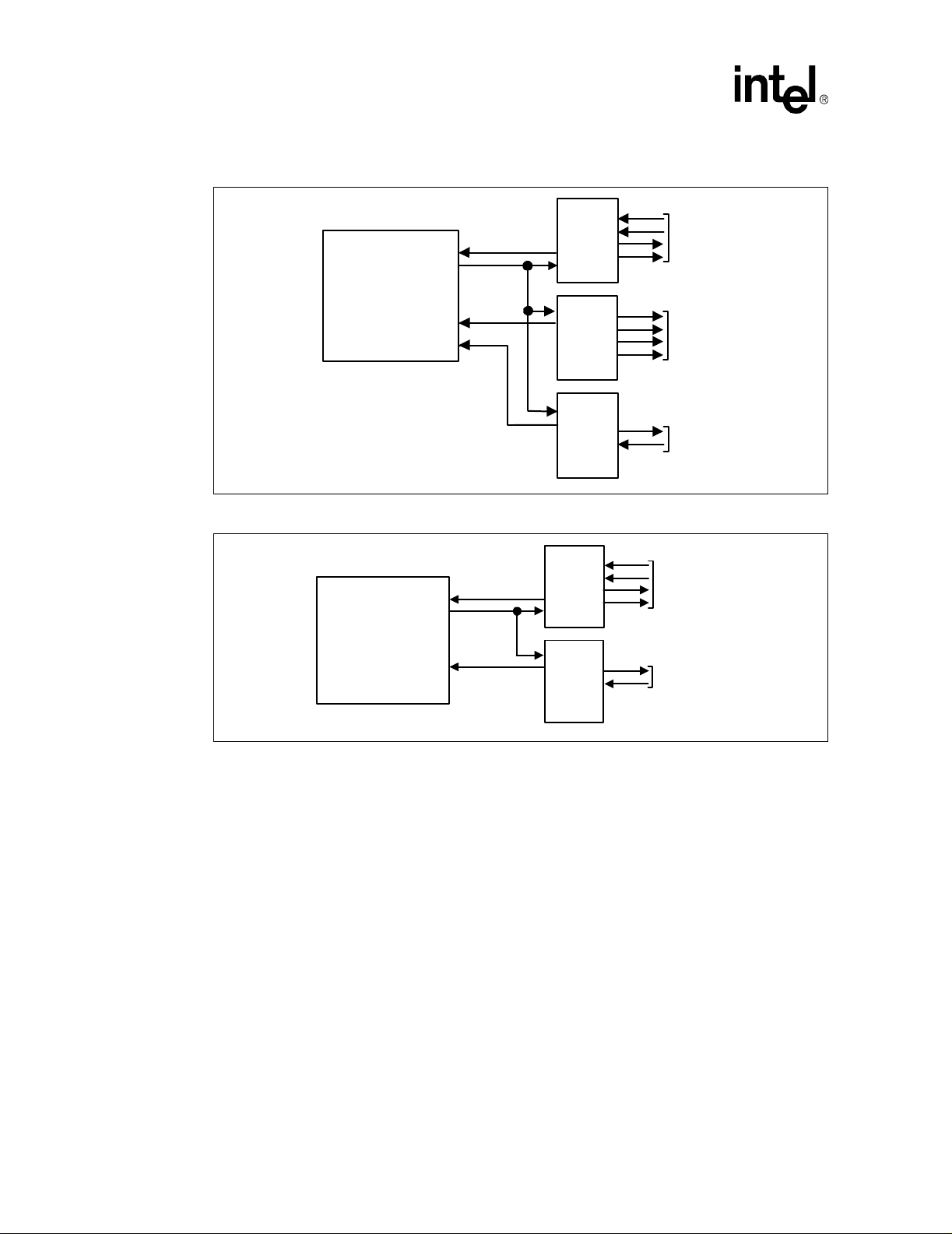
System Overview
Figure 2-3. AC '97 with 2 Audio and a Modem Codec (4 Channel Secondary)
®
Intel
ICH5
Figure 2-4. AC '97 with Audio and Modem Codec
®
Intel
ICH5
AC-link
AC-link
AC’97
Audio
CODEC
AC’97
Audio
CODEC
AC’97
Modem
CODEC
AC’97
Audio
CODEC
AC’97
Modem
CODEC
Audio
Port
Audio
Port
Modem
Port
Audio
Port
Modem
Port
32 Intel® 875P Chipset Platform Design Guide
2.3 Bandwidth Summary
Table 2- 1 and Table 2-3 provide a summary of the bandwidth requirements for the MCH and ICH5.
Table 2-2. MCH System Bandwidth Summary
System Overview
Interface
System Bus 200 4 8 6.4 GB/s
DDR-SDRAM 133/166/200 2 8 2.1 / 2.7 / 3.2 GB/s (per channel)
AGP 66 8 4 2.1 GB/s
CSA 66 4 1 266 MB/s
Clock Speed
(MHz)
Samples per
Clock
Table 2-3. Intel® ICH5 System Bandwidth Summary
Interface
Hub Interface 66 4 266 8 266
PCI 2.3 33 1 33 32 133
IDE
SATA 750 2 1500 1 150
LCI 5 - 50 1 5 - 50 3 1.875 – 18.75
AC ’97 12.288 1 12.288 1 1.536
LPC 33 1 33 4 16.5
USB 2.0 Highspeed
SMBus 10–16 kHz 1 10 1 1.25 KB/s
Clock Speed
(MHz)
Up to 44.444 Write
Up to 50 Read
Up to 240
(embedded in data)
Samples
Per Clock
1
Up to 2 480 1 60
Data Width
(Bytes)
Data Rate
(Mega-samples/s)
44.444 (Write)
50 (Read)
Bandwidth
Data Width
(Bits)
16
Bandwidth
(MB/s)
88.9 (Write)
100 (Read)
Intel® 875P Chipset Platform Design Guide 33
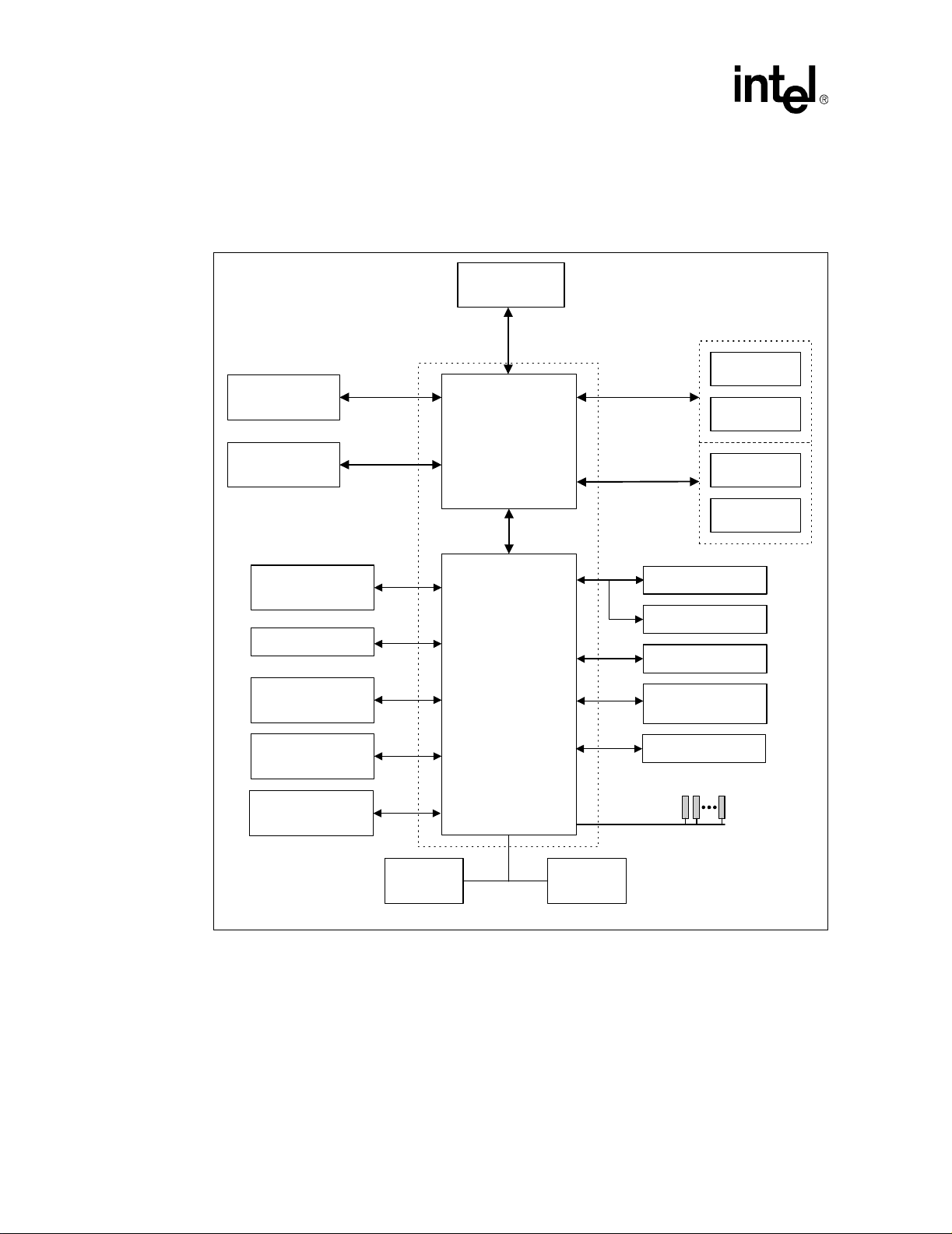
System Overview
2.4 System Configurations
Figure 2-5 illustrates a typical 875P chipset-based system configuration.
Figure 2-5. Typical System Configuration
Processor
AGP 8x/4x
CSA Interface
Gigabit Ethernet
USB 2.0
8 ports, 480 Mb/s
GPIO
2 Serial ATA Ports
150 MB/s
2 ATA 100 Ports
2.1 GB/s
266 MB/s
400/533/800 MHz
Front Side Bus
Intel® 82875P MCH
266 MB/s
HI 1.5
Intel® 82801EB
Intel
Intel® 875P Chipset
ICH5
or
®
82801ER
ICH5R
Channel A
2.1 GB/s
up to
3.2 GB/s
Channel B
2.1 GB/s
up to
3.2 GB/s
Power Management
Clock Generation
LAN Connect/ASF
System
Management (TCO)
SMBus 2.0/I2C
System Memory
DDR
DDR
DDR
DDR
Six PCI Masters
AC '97
3 CODEC support
Flash
BIOS
LPC
Interface
PCI Bus
SIO
34 Intel® 875P Chipset Platform Design Guide

Platform Stack-Up and Placement Overview
Platform Stack-Up and Placement Overview 3
In this chapter, an example of an 875P chipset platform component placement and stack-up is
presented for a desktop system in an ATX board form factor with dual-channel, DDR266/333/400
SDRAM memory capabilities.
3.1 General Design Considerations
This section documents motherboard layout and routing guidelines for the 875P chipset platform.
This section does not discuss the functional aspects of any bus, or the layout guidelines for an addin device.
Note: If the guidelines listed in this document are not followed, it is very important that thorough signal
integrity and timing simulations are completed for each design. Even when the guidelines are
followed, critical signals are recommended to be simulated to ensure proper signal integrity and
flight time. Any deviation from the guidelines should be simulated.
The trace impedance typically noted (i.e., 60 Ω ± 15%) is the “nominal” trace impedance for a
5-mil wide trace. That is, the impedance of the trace when not subjected to the fields created by
changing current in neighboring traces. When calculating flight times it is important to consider the
minimum and maximum impedance of a trace based on the switching of neighboring traces. Using
wider spaces between the traces can minimize this trace-to-trace coupling. In addition, these wider
spaces reduce settling time.
Coupling between two traces is a function of the coupled length, the distance separating the traces,
the signal edge rate, and the degree of mutual capacitance and inductance. To minimize the effects
of trace-to-trace coupling, the routing guidelines documented in this section should be followed.
Additionally, these routing guidelines are created using a PCB (Printed Circuit Board) stack-up as
illustrated in Figure 3-1.
3.2 Board Stack-Up
The 875P chipset platform requires a board stack-up yielding a target board impedance of
60 Ω ± 15%. Recommendations in this platform design guide are based on the following 4-layer
board stack-up. The stack-up numbers may vary, thus it is important to stay within the specified
tolerances.
Intel® 875P Chipset Platform Design Guide 35
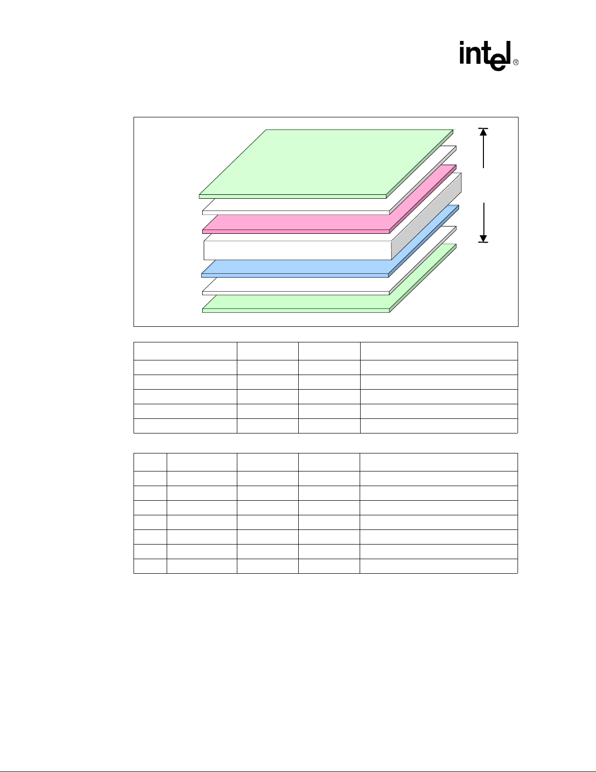
Platform Stack-Up and Placement Overview
Figure 3-1. 4-Layer PCB Stack-Up Example
Signal Layer
A
Prepreg
B
Power Layer
C
Core
D
Ground Layer
E
Prepreg
F
Signal Layer
G
Description Nominal Value Tolerance Comments
Board Impedance Z
Prepreg Dielectric Er 4.1 ± 0.3 @ 100 MHz
Soldermask Er 4.0 ± 0.5 @ 100 MHz
Soldermask Thickness 1.0 mil ± 0.5 mils From top of trace
Trace Width 5.0 mils ± 0.5 mils Standard trace
Layer Description Nominal Value Tolerance Comments
0
60 Ω ± 15% With nominal 5-mil trace width
Total
Thickness
62.3 mils
A Signal Layer 0.7 mils (See Note 2) 0.5 oz Cu (See note 1)
B Prepreg 4.4 mils ± 0.6 mils 1 sheet 2116 Pre-Preg
C Power Layer 1.4 mils ± 0.2 mils 1 oz unplated Cu
D Core 47 mils ± 5.0 mils 6 sheets 7628 Prepreg (7.8 ± 0.5 mils)
E Ground Layer 1.4 mils ± 0.2 mils 1 oz unplated Cu
F Prepreg 4.4 mils ± 0.6 mils 1 sheet 2116 Pre-Preg
G Signal Layer 0.7 mils (See Note 2) 0.5 oz Cu (See note 1)
NOTES:
1. Thickness before plating
2. Final Plating Thickness varies 1.3 mils – 1.42 mils (need 1.85 mils total)
36 Intel® 875P Chipset Platform Design Guide
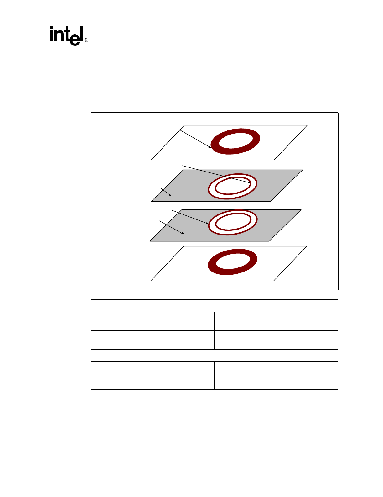
3.2.1 PCB Technology Considerations
Intel has found that the following recommendation aids in the design of a 875P chipset-based
platform. Simulations and reference platform are based on the following technology and is
recommended that designers adhere to these guidelines.
Figure 3-2. PCB Technologies Stack-Up
Platform Stack-Up and Placement Overview
Copper (pad)
Finished hole
Copper
Anti- Pad
Copper
L1
L2
L3
L4
Number of Layers
Stack-Up 4 Layer
Cu Thickness 0.5 oz outer (plated); 1 oz Inner
Final Board Thickness 62.3 mils (± 5 mils)
Material Fiberglass made of FR4
Signal and Power Via Stack
Via Pad 25 mils
Via Anti-Pad 40 mils
Via Finished Hole 14 mils
Intel® 875P Chipset Platform Design Guide 37
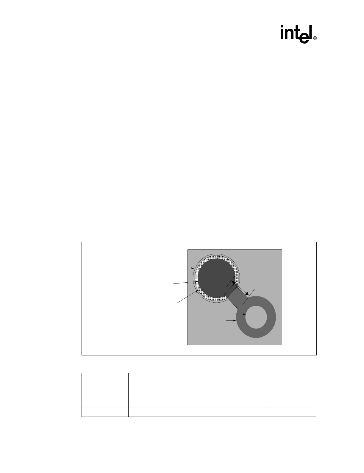
Platform Stack-Up and Placement Overview
p
3.2.2 Component Motherboard Layout (Pads and Vias)
Intel currently recommends non-soldermask defined pads (metal defined pads) with “dog-bone”
connecting vias for its chipsets. When compared to solder mask defined pads, non-soldermask
defined pads offer improved solder-joint reliability.
The solder mask opening and the registration accuracy of that opening relative to the pad is critical
to ensure good solder joints and minimize shorting. If the opening is too large, misregistration may
uncover a nearby trace increasing the possibility of a short occurring. Regardless of opening size,
misregistration may cause soldermask material to cover part or the entire pad, yielding a joint with
a poor cross-section (reliability) or a complete open.
Tips
• Inconsistent soldermask coverage between the via and pad may lead to top and bottom side
tenting in order to avoid accidentally wicking the solder ball into the via-hole creating an open
or unreliable joint. Tenting both sides may trap moisture in the via during reflow causing
severe soldermask damage as it vents. One solution is to ensure that the raw printed circuit
boards are dry; an alternative is to allow for a small topside vent-hole (pin-hole) in the tenting.
• A reliability consideration to take into account when choosing a pad size: The pad size also
affects the joint height; a smaller pad forces a taller joint. There are industry claims that a taller
joint increases the mechanical flexibility of the joint and thus may improve power cycle and
temperature cycle joint life.
• Solder mask must cap the vias on the bottom side of the board to minimize heat transfer to the
solder.
Figure 3-3. Via-Pad Layout Metal-Defined Pads
solder ball diameter
board pad diameter
finished solder
mask diameter
standard diameter via plated
IMPORTANT:
Solder mask MUST cap
the via on bottom side.
optional, but advised, on
onent side.
com
standard diameter via pad
Table 3-1. Via-Pad Layout Metal-Defined Pads
Component Solder Ball Pitch
Processor 1.27 mm 30 mils 20 mils 22 – 26 mils
MCH 1.27 mm 24 mils 18 mils 20 – 24 mils
®
ICH5 1.27 mm 30 mils 20 – 24 mils 24 – 27mils
Intel
Solder Ball
Diameter
Solder mask dam
Min = 4 mils to
prevent solder
thieving
Board Pad
Diameter
Finished Solder
Mask Diameter
38 Intel® 875P Chipset Platform Design Guide
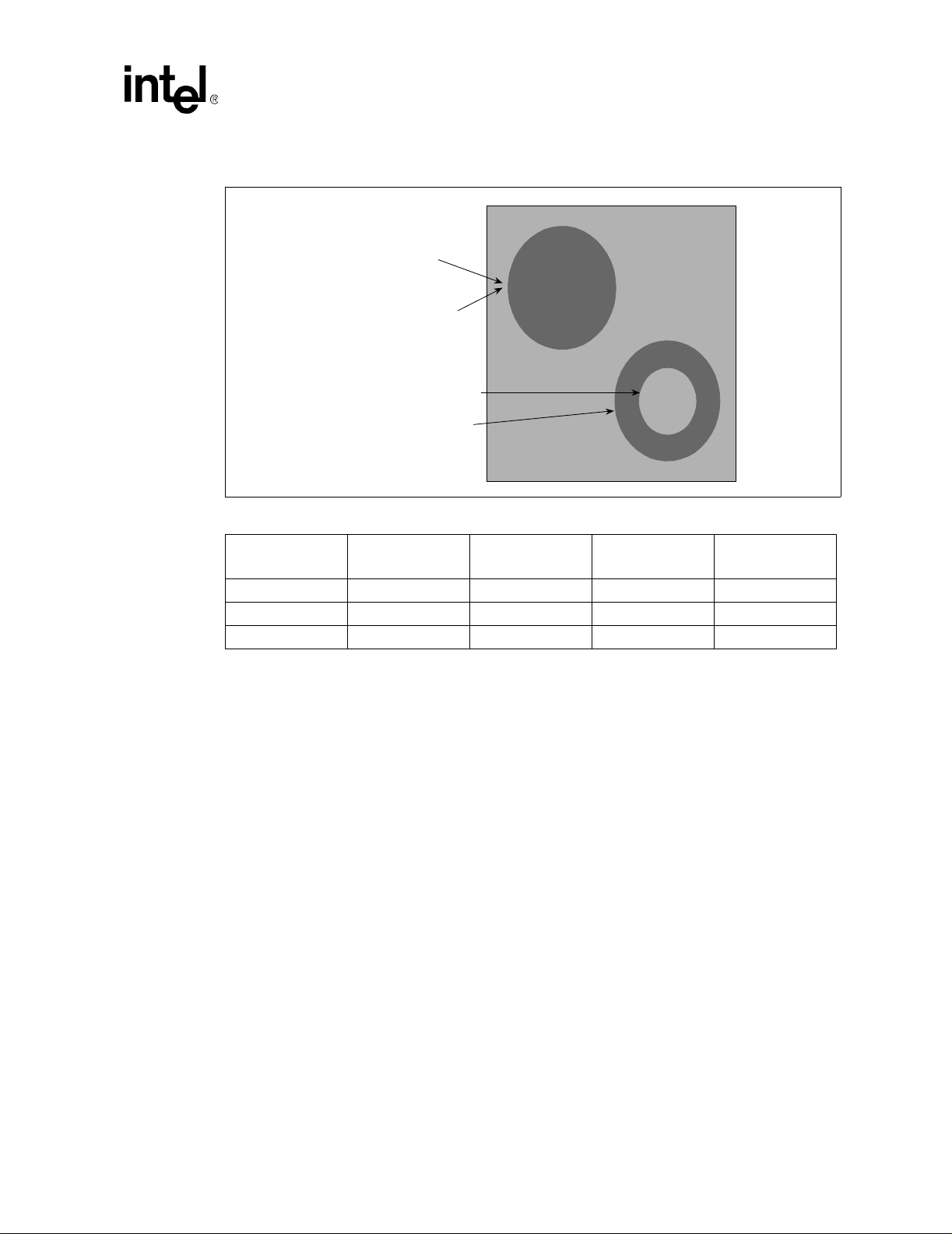
Figure 3-4. Via-Pad Layout Solder Mask-Defined Pads
Platform Stack-Up and Placement Overview
board pad
diameter
finished solder
mask diameter
standard diameter via plated
standard diameter via pad
Table 3-2. Via-Pad Layout Solder Mask-Defined Pads
Component Solder Ball Pitch
Processor 1.27 mm 30 mils 22 – 26 mils 22 – 26 mils
MCH 1.27 mm 24 mils 18 mils 18 mils
®
ICH5 1.27 mm 30 mils 20 – 24 mils 20 – 24 mils
Intel
Solder Ball
Diameter
Solder mask
over copper
flood
Board Pad
Diameter
Finished Solder
Mask Diameter
Intel® 875P Chipset Platform Design Guide 39
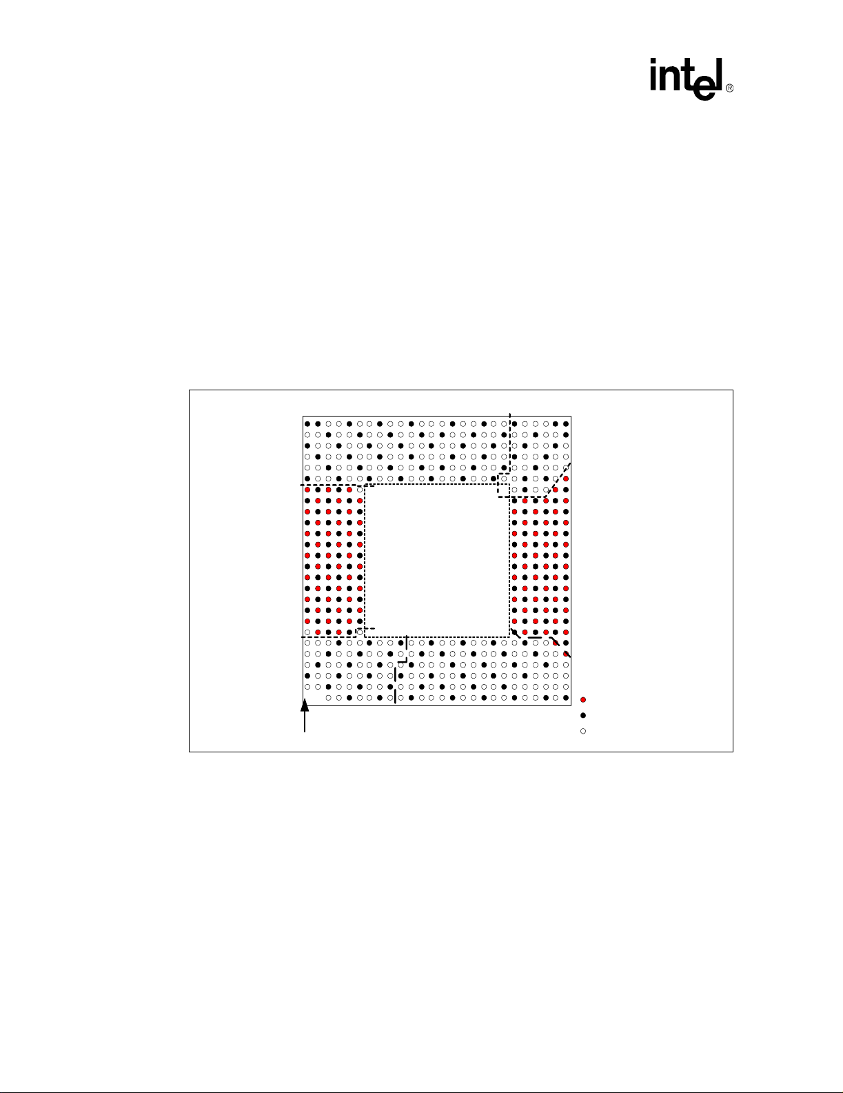
Platform Stack-Up and Placement Overview
3.3 Component Quadrant Layout
The preliminary quadrant layouts shown are approximations. The quadrant layout figures do not
show the exact component ball count; only general quadrant information is presented and is
intended for reference while using this document. Only the exact pin or ball assignment should be
used to conduct routing analysis. Reference to the appropriate component datasheet for pin or ball
assignment information.
3.3.1 Processor Quadrant Layout
Figure 3-5 illustrates the quadrant layout of the Pentium 4 processor with 512-KB L2 cache on
0.13 micron process, the Pentium 4 processor Extreme Edition supporting Hyper-Threading
Technology, and the Pentium 4 processor on 90 nm process.
Figure 3-5. Processor Component Quadrant Layout (Top View)
Data
Clocks
Vcc/Vss
Common
Clock
Pin 1
Processor
Top View
Address
=Power
=GND
=Signal
40 Intel
®
875P Chipset Platform Design Guide
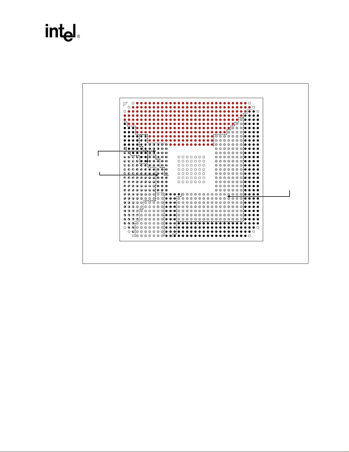
Platform Stack-Up and Placement Overview
3.3.2 MCH Component Quadrant Layout
Figure 3-6. MCH Component Quadrant Layout (Top View)
Vcc AGP
Vcc Core
Vcc HI
AGP
System Bus
333231302928272625242322212019181716151413121110987654321
A
B
C
D
E
F
G
H
J
K
L
M
N
P
R
T
U
V
W
Y
AA
AB
AC
AD
AE
AF
AG
AH
AJ
AK
AL
AM
AN
HI / CSA
DDR Channel A
A
B
C
D
E
F
G
H
J
K
L
M
N
P
R
T
U
V
W
Y
AA
DDR Channel B
AB
AC
AD
AE
AF
AG
AH
AJ
AK
AL
AM
AN
333231302928272625242322212019181716151413121110987654321
Intel® 875P Chipset Platform Design Guide 41

Platform Stack-Up and Placement Overview
3.3.3 Intel® ICH5 Component Quadrant Layout
Figure 3-7. Intel® ICH5 Quadrant Layout (Top View)
Pin 1
PCI
Flash BIOS /
LPC
GPIO
SMBUS
S-ATA
LAN /
AC'97
POWER
USB
HI
CPU
RTC
IDE
42 Intel
®
875P Chipset Platform Design Guide

Platform Stack-Up and Placement Overview
3.4 Platform Component Placement
Figure 3-8. Component Placement Example Using a 4-DIMM ATX Board
Intel® 875P Chipset Platform Design Guide 43

Platform Stack-Up and Placement Overview
This page is intentionally left blank.
44 Intel
®
875P Chipset Platform Design Guide

Platform Clock Routing Guidelines
Platform Clock Routing Guidelines 4
To minimize jitter, improve routing, and reduce cost, 875P chipset-based systems should use a
single-chip clock solution, the CK409. In this configuration, the CK409 provides three
100/133/200-MHz selectable differential outputs pairs for all of the host bus agents, one 100-MHz
differential output pair for serial ATA, two 48-MHz clocks, five 66-MHz clocks, ten 33-MHz
clocks, and two 14-MHz clocks. Figure 4-1 shows the implementation of the clocks for a typical
875 chipset platform.
For more information on CK409 compliance, refer to the CK409 Clock Synthesizer/ Driver
Specification Document.
Table 4-1. Intel
Host_CLK 100/133/200 Processor, Debug Port, and MCH
CLK66 66
CLK33_ICH5 33 ICH5
CLK14 14.318 ICH5 and SIO
CLK33 33 PCI Connectors, SIO, and Flash BIOS
DOTCLK 48 MCH
SRC 100 ICH5-Serial ATA
USBCLK 48 ICH5
®
875 Chipset Clock Group
Clock Name
Frequency
(MHz)
MCH, Intel
connector
Receiver
®
ICH5, Intel® 82547EI GbE controller and AGP
Intel® 875P Chipset Platform Design Guide 45

Platform Clock Routing Guidelines
Figure 4-1. Intel® 875P Chipset-Based System Clocking Diagram
14.318MHz
CK409
100/133/200 MHz, Diff Pair
100/133/200 MHz, Diff Pair
100/133/200 MHz, Diff Pair
66 MHz, 3.3V, SE (3V66/VCH)
48 MHz, 3.3V, SE
66 MHz, 3.3V, SE
66 MHz, 3.3V, SE
48 MHz, 3.3V, SE, USB 2.0
33 MHz, 3.3V, SE, PCI/LPC
14.318 MHz, 3.3V, SE, Timers
66 MHz, 3.3V, SE
33 MHz, 3.3V, SE
33 MHz, 3.3V, SE
33 MHz, 3.3V, SE
33 MHz, 3.3V, SE
33 MHz, 3.3V, SE
33 MHz, 3.3V, SE
33 MHz, 3.3V, SE
33 MHz, 3.3V, SE
Intel 82547EI
Flash BIOS
PCI Down
PCI slot 1
PCI slot 2
PCI slot 3
PCI slot 4
PCI slot 5
AGP 4/8X
Processor
MCH
®
Intel
ICH5
32.768 KHz
ITP
HI
Memory
Slot 0
Slot 1
DDR 4 slots
12 diff CLKs
SDR 4 slots
16 SE CLKs
12.288 MHz AC97
SUSCLK
SIO
Slot 2
Slot 3
100 MHz, Diff Pair SRC
FS_A
FS_B
PCI_Stop#
CPU_Stop#
PWRDWN#
Vtt_PWRGD#
46 Intel
AC97
®
875P Chipset Platform Design Guide

4.1 HOST_CLK Clock Group
4.1.1 HOST_CLK Clock Topology
The clock synthesizer provides three sets of 100/133/200-MHz differential clock outputs. The
differential clocks are driven to the processor, the 875P chipset, and the processors’ debug ports as
shown in Figure 4-1.
The clock driver differential bus output structure is a “Current Mode Current Steering” output that
develops a clock signal by alternately steering a programmable constant current to the external
termination resistors “Rt.”
The recommended termination for the differential bus clock is a “Shunt Source Termination.”
Refer to Figure 4-2 for an illustration of this terminology scheme. Parallel Rt resistors perform a
dual function, converting the current output of the clock driver to a voltage, and matching the
driver output impedance to the transmission line. The series resistors “Rs” provide isolation from
the clock driver's output parasitics that would otherwise appear in parallel with the termination
resistor Rt.
The value of Rt should be selected to match the characteristic impedance of the motherboard, and
Rs should be 33 Ω. Simulations have shown that Rs values above 33 Ω provide no benefit to signal
integrity but only degrade the edge rate.
Platform Clock Routing Guidelines
• IREF pin (pin # 41) is connected to ground through a 475 Ω ± 1% resistor – making the IREF
2.32 mA
For more information on CK409 compliance, refer to the CK409 Clock Synthesizer/ Driver
Specification Document.
The CK409 allows for different host clock frequencies. The FS_A and FS_B pins on the CK409
control the output host clock frequencies. See Table 4-2 for different CK409 host clock frequency
configurations.
Table 4-2. Host Clock Frequency Select on CK409
FS_A FS_B
0 0 100 MHz
1 0 133 MHz
0 1 200 MHz
Host Clock
Frequency
Intel® 875P Chipset Platform Design Guide 47
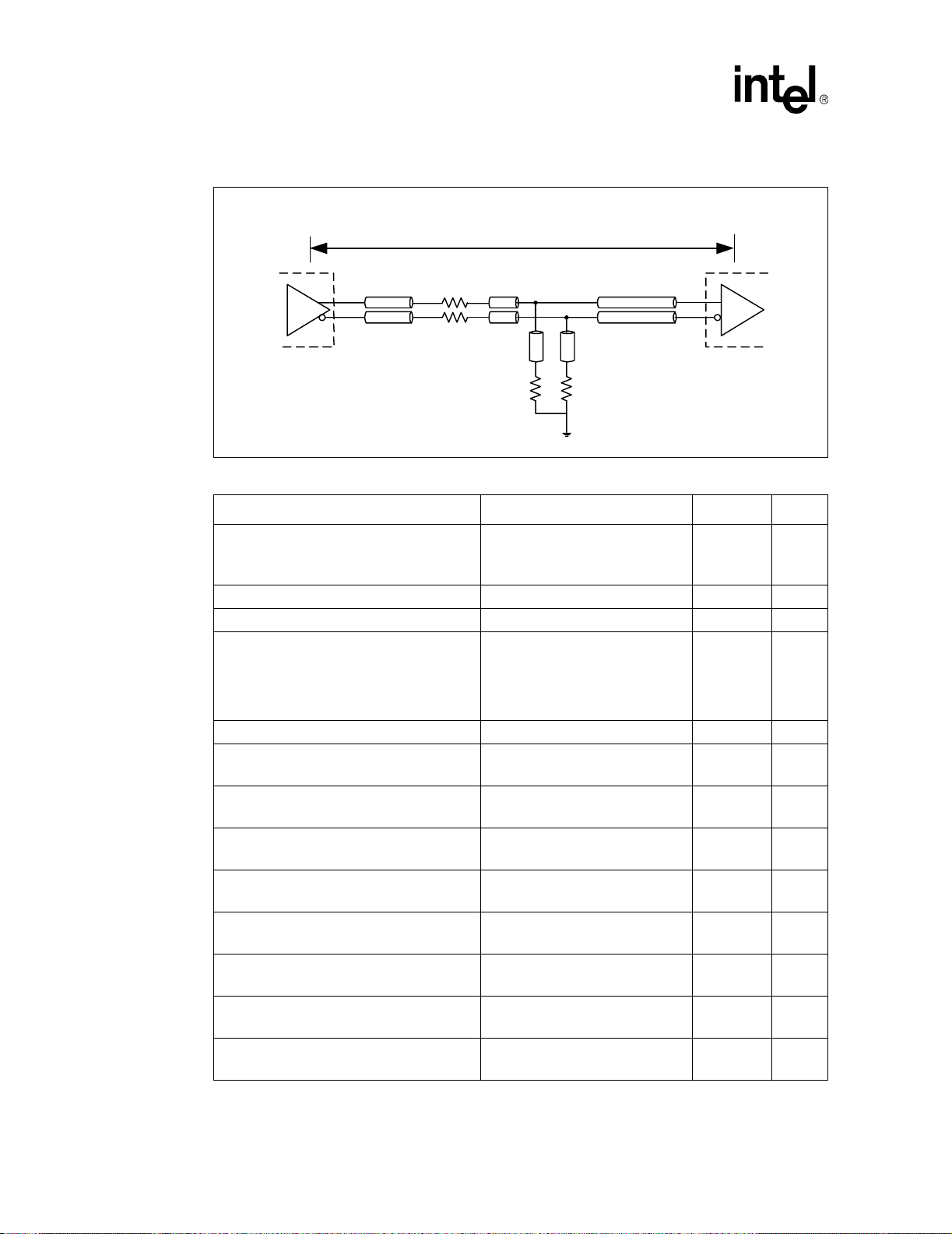
Platform Clock Routing Guidelines
Figure 4-2. Source Shunt Termination
LT = L1 + L2 + L4
Rs
Rs
L2
L2'
L3
Rt Rt
L3'
Clock
Driver
L1
L1'
Table 4-3. HOST_CLK[1:0]# Routing Guidelines (Sheet 1 of 2)
Layout Guideline Value Illustration Notes
300 ps total budget:
HOST_CLK Skew between Agents
Differential Pair Spacing 11 mils Figure 4-3 5,7
Spacing to Other Traces 25 mils Figure 4-4
Serpentine Spacing
Motherboard Impedance – Differential 120
Processor Routing Length –
L1, L1’: Clock Driver to Rs
Processor Routing Length –
L2, L2’: Rs to Rs-Rt Node
Processor Routing Length –
L3, L3’: Rs-Rt Node to Rt
Processor Routing Length –
L4, L4’: Rs-Rt Node to Load
MCH Routing Length –
L1, L1’: Clock Driver to sS
MCH Routing Length –
L2, L2’: Rs to Rs-Rt Node
MCH Routing Length –
L3, L3’: Rs-Rt Node to Rt
MCH Routing Length –
L4, L4’: Rs-Rt Node to Load
150 ps for clock driver
150 ps for interconnect
Maintain a minimum 25 mils
Keep parallel serpentine sections as
short as possible.
Minimize 90-degree bends. Make
45-degree bends if possible.
Ω 7
0.5 inch max Figure 4-2 9
0 – 0.2 inch Figure 4-2 9
0 – 0.2 inch Figure 4-2 9
2 – 15 inches Figure 4-2
0.5 inch max Figure 4-2 9
0 – 0.2 inch Figure 4-2 9
0 – 0.2 inch Figure 4-2 9
2– 15 inch Figure 4-2
L4
L4'
Processor
or MCH
Figure 4-2
and
Figure 4-3
1,2,3,4
48 Intel
®
875P Chipset Platform Design Guide
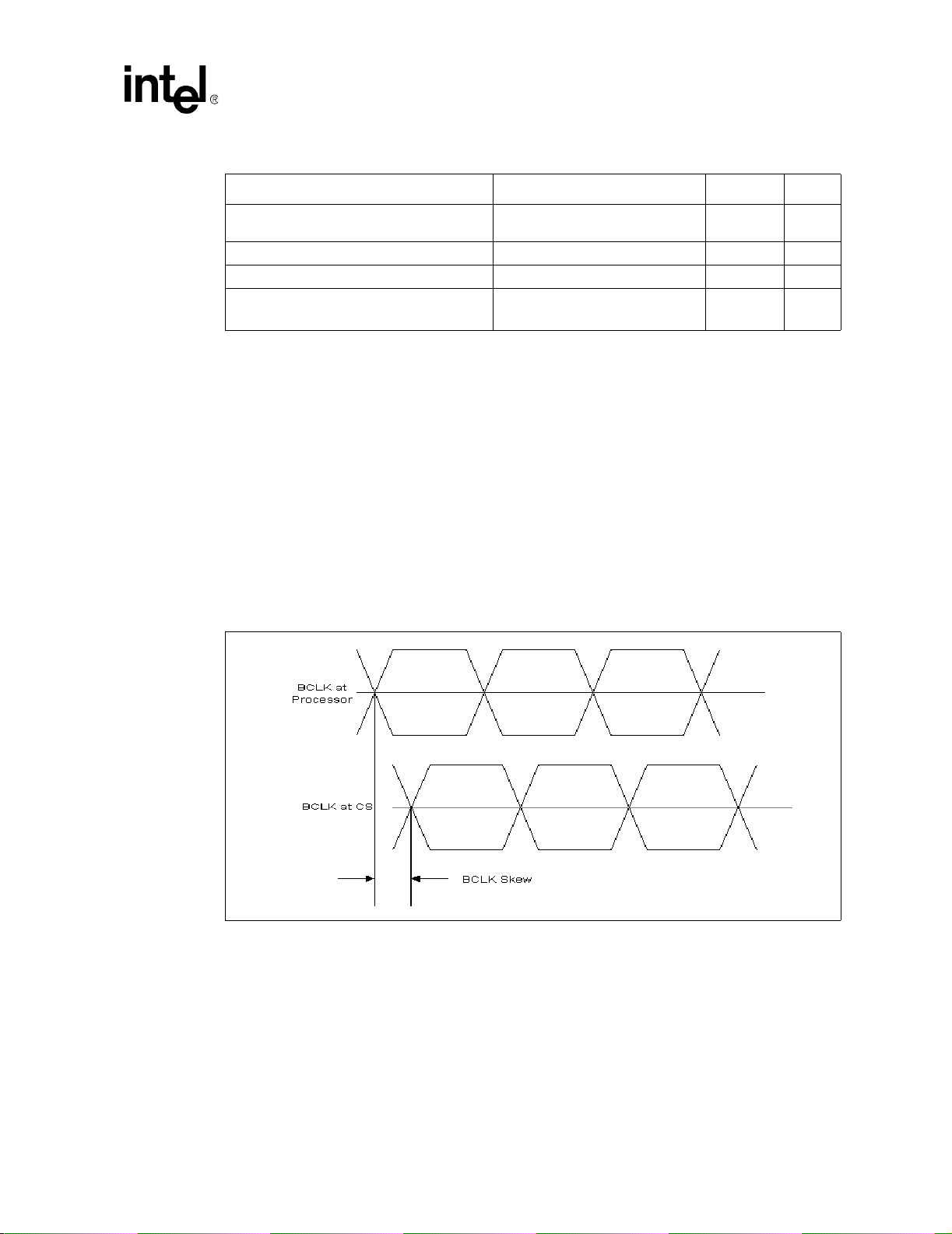
Table 4-3. HOST_CLK[1:0]# Routing Guidelines (Sheet 2 of 2)
Layout Guideline Value Illustration Notes
Processor to MCH Length Matching (LT)
HOST_CLK0 – HOST_CLK1 Length Matching ± 10 mils
Rs Series Termination Value 33
Rt Shunt Termination Value
NOTES:
1. The skew budget includes clock driver output pair to output pair jitter (differential jitter) and skew, clock skew
due to interconnect process variation, and static skew due to layout differences between clocks to all bus
agents.
2. This number does not include clock driver common mode (cycle-to-cycle) jitter or spread spectrum clocking.
3. The interconnect portion of the total budget for this specification assumes clock pairs are routed on multiple
routing layers and routed no longer than the maximum recommended lengths.
4. Skew measured at the load between any two-bus agents. Measured at the crossing point.
5. Clock traces are routed in a differential configuration. Maintain the minimum recommended spacing between
the two traces of the pair. Uniform spacing should be maintained along the entire length of the trace. Do not
exceed the maximum trace spacing, as this will degrade the noise rejection of the network.
6. Set line width to meet the proper trace impedance based on the recommended stack up.
7. The differential impedance of each clock pair is approximately 2*Zsingle-ended*(1–2*Kb) where Kb is the
backwards cross-talk coefficient. For the recommended trace spacing, Kb is very small, and the effective
differential impedance is approximately equal to 2 times the single-ended impedance of each half of the pair.
8. The host clocks to the processor must be 150 mils longer than the host clocks to the MCH.
9. Minimize L1, L2 and L3 lengths. Long lengths on L2 and L3 degrade effectiveness of source termination and
contribute to ringback.
Host clocks to
150 mils
Ω ± 5% Figure 4-2
Ω± 1%
49.9
(for 50
processor should be
longer
Ω odd mode MB impedance)
Platform Clock Routing Guidelines
Figure 4-2 8
Figure 4-2
Figure 4-3. Clock Skew As Measured from Agent to Agent
Intel® 875P Chipset Platform Design Guide 49
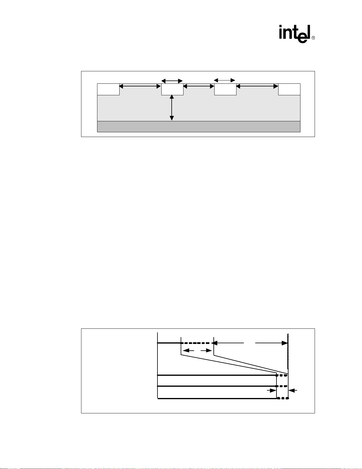
Platform Clock Routing Guidelines
Figure 4-4. Trace Spacing for HOST_CLK Clocks
S1
WW
BCLK0 BCLK1
h
S
S1
Ground Plane
4.1.2 BCLK General Routing Guidelines
• When routing the 100/133/200-MHz selectable differential clocks, do not split up the two
halves of a differential clock pair between layers, and route to all agents on the same physical
routing layer referenced to ground.
• If a layer transition is required, make sure to do simulations to determine the skew induced by
the vias used to transition between routing layers is compensated in the traces to other agents.
• Also, if a layer transition is required then both clock traces must transition layers so that
differential routing is maintained.
4.2 CLK66 and CL33 Clock Groups
4.2.1 Length Matching
When routing the 33 MHz and 66 MHz clock group signals, it is important to understand the length
matching relationships between all of these signals. Trace length matching is required in each
group to help minimize skew and ensure good signal integrity.
4.2.1.1 CLK_66 and Intel® ICH5 CLK_33 Length Matching
Figure 4-5. 66 MHz/33 MHz Clock Relationships
3V66 (AGP C onnec tor)
1"
3V66 ((G)MCH)
3V66 (Int el® ICH5, CSA)
PCI ( to ICH5)
50 Intel
5" length c om pensates
f or add-in c ard rout ing
Y
Z
®
875P Chipset Platform Design Guide
5"
0.5"
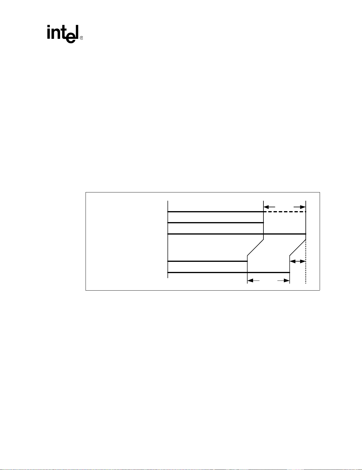
NOTES:
1. Length “Y” denotes the 66 MHz clock length to the (G)MCH and dictates the lengths of the 66 MHz clocks
and length “Z” to the ICH5.
2. Length “Z” denotes the 33 MHz clock length to the ICH5 and dictates the lengths of the 33 MHz clocks.
If Y is the length of the 66 MHz clock length to the (G)MCH, then the 66 MHz clocks to CSA,
AGP, and ICH5, as well as the 33 MHz clock to the ICH5 (length “Z”), should be length matched
to Y ± 0.5 inches. These lengths are strictly dependant on their clock matching relationships to the
(G)MCH. AGP add-in card routing (including connector) reduces motherboard trace length by
5 inches, thus maximum routable mismatch to the AGP connector is Y – 5 ± 0.5 inches. In
addition, designers are allowed up to an additional inch of routing flexibility to meet AGP timing
specifications.
Thus, if Y is 9 inches, then CLK_66 to CSA can be anywhere between 8.5 to 9.5 inches, while
CLK_66 to AGP is routed between 3.5 to 4.5 inches. This minimum length may decrease an
additional inch to 2.5 inches based on simulation results.
4.2.1.2 CLK_33 Length Matching
Figure 4-6. 33 MHz Clock Relationships
Platform Clock Routing Guidelines
Z
PCI ( to Intel® ICH5)
PCI (Down) Short est Length
PCI (Down) Longest Length
4" length
PCI (Connec tor) Short est Length
PCI (Connect or) Longest Length
NOTE: Length “Z” denotes the 33 MHz clock length to the ICH5 and dictates the lengths of the 33 MHz clocks.
compensates for
add-in card
routing
10"
10"
4"
The 33 MHz clock group signals should be length matched up to a maximum of 10 inches. Length
“Z” denotes the 33 MHz clock to the ICH5 and will dictate the length of all other 33 MHz clock
signals. PCI add-in card routing and connector routing reduces the total allowable motherboard
trace length by 4 inches. If the CLK_33 length to the ICH5 is 17 inches, then the shortest allowable
routed motherboard length to any PCI slot is 17– 10 – 4 = 3 inches. Likewise, if the CLK_33 length
to the ICH5 is 5 inches trace, then the longest allowable routed length to any PCI slot is
5+ 10– 4 = 11 inches.
Intel® 875P Chipset Platform Design Guide 51
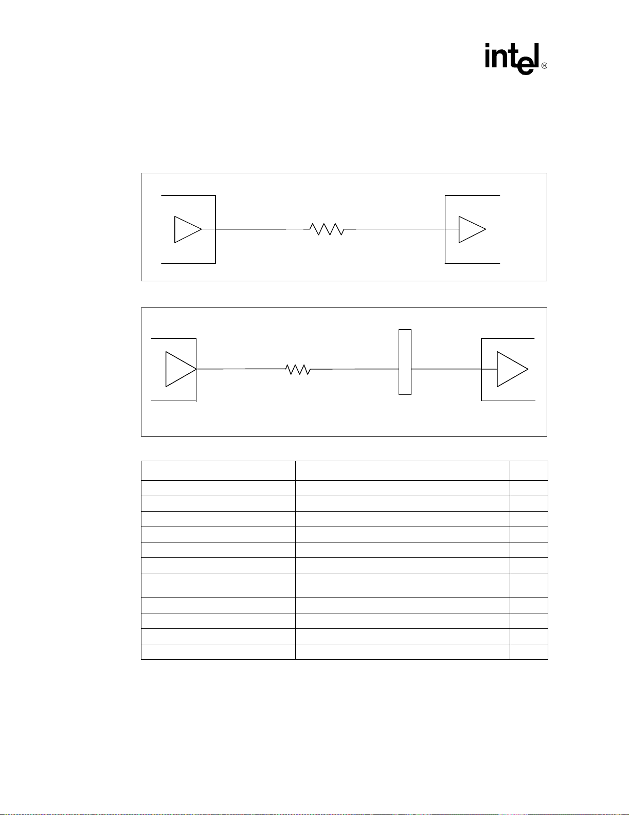
Platform Clock Routing Guidelines
4.2.2 TCLK33 Clock Group
For the CLK33 clock group, the driver is the clock synthesizer 33-MHz clock output buffer, and
the receiver is the 33-MHz clock input buffer at the various down devices and the PCI slots.
Figure 4-7. Topology for CLK33 to Down Devices
L1 L2
Clock
Driver
Figure 4-8. Topology for CLK33 to PCI Slot
L1
Clock
Driver
R1
Table 4-4. CLK33 Routing Guidelines to Intel
Parameter Routing Guidelines Notes
Clock Group CLK33
Topology Point-to-Point
Reference Plane Ground referenced (contiguous over entire length)
Characteristic Trace Impedance (Z
Trace Width 5 mils
Trace Spacing 10 mils
®
ICH5, Flash BIOS, SIO, PCI slots
Intel
Trace Length – L1
Intel ICH5 – L2 Z; 2 inches to 20 inches 1
Flash BIOS, SIO Trace Length – L2 Z + (0 inch to 10 inches); max length is 20 inches 1
PCI slots Trace Length – L2 Z + (0 inch to 6 inches); max length is 20 inches 1
Resistor R1 = 33
) 60 Ω ± 15%
0
0 inch to 0.5 inch
R1
L2 C
Trace on PCI
Card
PCI
Connector
®
ICH5, Flash BIOS, SIO, and PCI Slots
Ω ± 5%
Inte l
FWH, & SIO
®
ICH5,
PCI Device
NOTES:
1. Refer to Figure 4-5 for length of “Z.”
52 Intel
®
875P Chipset Platform Design Guide

4.2.2.1 Sharing 33-MHz Clocks
In some cases the motherboard designer may have a need to share one PCI 33-MHz clock between
two PCI down devices. In this case the driver is the clock synthesizer 33-MHz clock output buffer,
and the receivers are the 33-MHz clock input buffers of two, separate PCI down devices.
Figure 4-9. Topology for Sharing CLK33 between Two PCI Down Devices
Platform Clock Routing Guidelines
L2
Clock
Driver
L1
R1
L3
Table 4-5. CLK33 Routing Guidelines for Sharing CLK33 between Two PCI
Down Devices
Parameters Routing Guidelines
Clock Group CLK33
Topology “T”
Reference Plane Ground referenced (contiguous over entire length)
Characteristic Trace Impedance (Z
Trace Width 5 mils
Trace Spacing 10 mils
Resistor 33
PCI Down Devices– L1 0 inch to 0.5 inch; max length is 20 inches
PCI Down Devices – L2 and L3
)60 Ω ± 15%
0
Ω ± 5%
Z + (0 inch to 7 inches); max length is 20 inches. L2 and L3 should
be length matched to within 250 mils.
PCI
down
devi ce
PCI
down
devi ce
NOTES:
1. Length “Z” is the distance from the 33-MHz clock driver to the ICH5, 33-MHz input buffer. “Z” can be 2 inches
to 20 inches long.
Intel® 875P Chipset Platform Design Guide 53
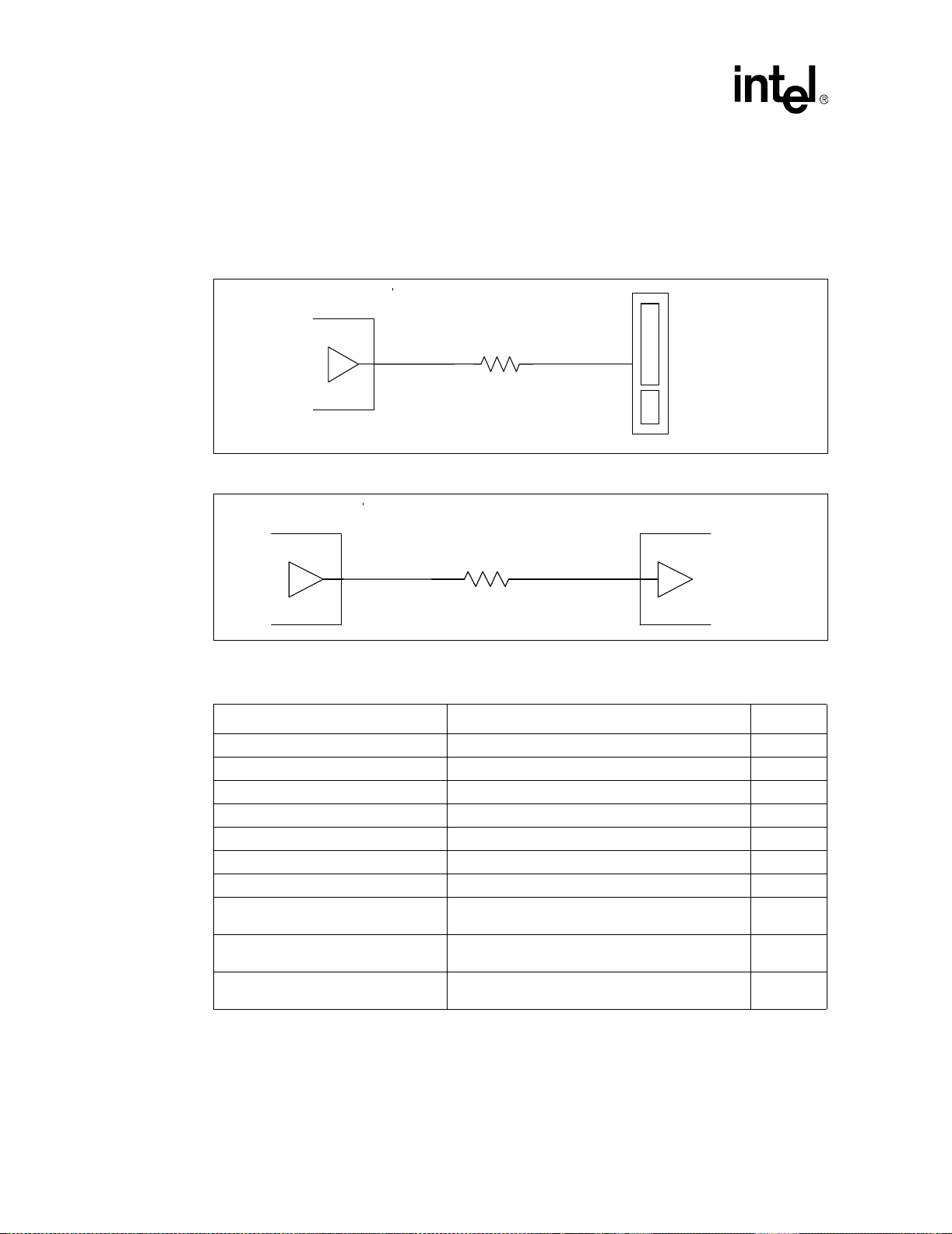
Platform Clock Routing Guidelines
4.2.3 CLK66 Clock Group
In the CLK66 clock group, the driver is the clock synthesizer 66-MHz clock output buffer, and the
receiver is the 66-MHz clock input buffer at the MCH, ICH5, the AGP connector and the 82547EI
GbE controller.
Figure 4-10. Topology for CLK66 to AGP Connector
Clock
Driver
Figure 4-11. Topology for CLK66 to MCH, Intel
Clock
Driver
Table 4-6. CLK66 Routing Guidelines for CLK66 to MCH, Intel
®
Intel
82647EI GbE Controller and AGP Connector
L1 L2
R1
®
ICH5, and Intel® 82647EI GbE Controller
L1 L2
R1
Parameters Routing Guidelines Notes
Clock Group CLK66
Topology Point-to-Point
Reference Plane Ground referenced (contiguous over entire length)
Characteristic Trace Impedance (Z
)60 Ω ± 15%
0
Trace Width 5 mils
Trace Spacing 10 mils
Resistor 33
AGP Connector, MCH, Intel
®
ICH5,
CSA Trace Length – L1
Clock Driver to MCH, ICH5, and GbE
Trace Length – L2
Clock Driver to AGP Connector Trace
Length – L2
Ω ± 1%
0 inch to 0.5 inch
Z - (0.5 inch to 0 inch); max length is 20 inches 1
Z - (6 inches to 5 inches); max length is 20 inches 1
®
ICH5,
AGP
connector
MCH,
Intel
®
Intel
®
ICH 5,
82547EI
NOTES:
1. Length “Z” is the distance from the 33-MHz clock driver to the ICH5 33-MHz input buffer. Refer to Figure 4-5.
“Z” can be 2 inches to 20 inches long.
54 Intel
®
875P Chipset Platform Design Guide
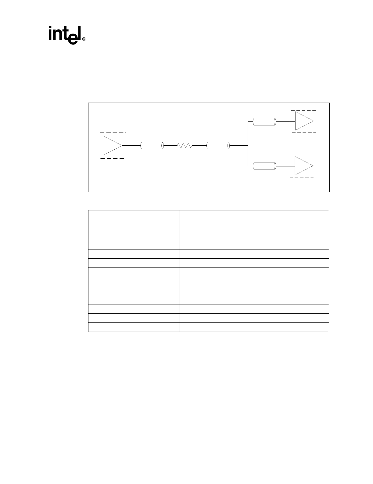
4.2.4 CLK14 Clock Group
The driver in the CLK14 clock group is the clock synthesizer 14.318-MHz clock output buffer, and
the receiver is the 14.318-MHz clock input buffer at the ICH5 and SIO.
Figure 4-12. Topology for CLK14
L1
R1
Platform Clock Routing Guidelines
L3
®
ICH5
Intel
L2
Clock
Driver
Table 4-7. CLK14 Routing Guidelines
Parameter Routing Guidelines
Clock Group CLK14
Topology Balanced T Topology
Reference Plane Ground referenced (contiguous over entire length)
Characteristic Trace Impedance (Z
Trace Width 5 mils
Trace Spacing 10 mils
Trace Length – L1 0 inch to 0.5 inch
Trace Length – L2 0 inch to 12 inches
Trace Length – L3 0 inch to 6 inches
CLK14 Total Length (L1+L2+L3) (L1+L2+L3) to ICH5 must be within 500 mils of (L1+L2+L3)to SIO
Resistor 33
Skew Requirements None
)60 Ω ± 15%
0
Ω ± 5%
L3
SIO
Intel® 875P Chipset Platform Design Guide 55
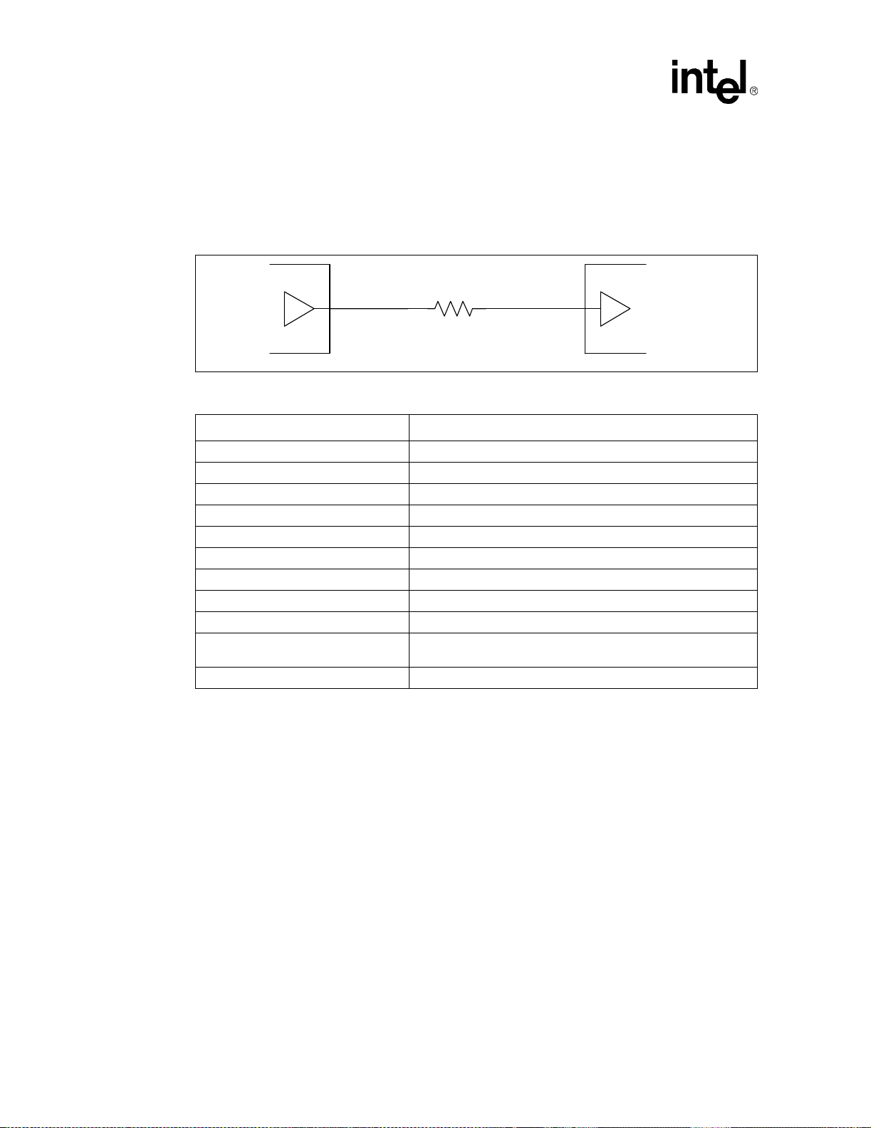
Platform Clock Routing Guidelines
4.2.5 USB Clock Group
For the USBCLK clock group, the driver is the clock synthesizer USB clock output buffer, and the
receiver is the USB clock input buffer at the ICH5. Note that this clock is asynchronous to any
other clock on the board.
Figure 4-13. Topology for USBCLK
L1 L2
Clock
Driver
Table 4-8. USBCLK Routing Guidelines
Parameter Routing Guideline
Clock Group USBCLK
Topology Point-to-Point
Reference Plane Ground referenced (contiguous over entire length)
Characteristic Trace Impedance (Z
Trace Width 5 mils
Trace Spacing 20 mils
Trace Length – L1 0 inch to 0.5 inch
Trace Length – L2 2 inches to 20 inches
Resistor R1 = 22
Skew Requirements
Maximum Via Count 2
4.2.6 SRC Clock Group
R1
)60 Ω ± 15%
0
Ω ± 1%
None – DOTCLK and USBCLK is asynchronous to any other clock
on the board
Intel
MCH,
®
ICH5
4.2.6.1 SRC Clock Topology
The clock synthesizer provides one set of 100-MHz differential clock outputs. The differential
clocks are driven to the ICH5 for serial-ATA as shown in Figure 4-1.
The clock driver differential bus output structure is a “Current Mode Current Steering” output that
develops a clock signal by alternately steering a programmable constant current to the external
termination resistors “Rt.”
The recommended termination for the differential bus clock is a “Shunt Source Termination.”
Refer to Figure 4-14 for an illustration of this terminology scheme. Parallel Rt resistors perform a
dual function, converting the current output of the clock driver to a voltage and matching the driver
output impedance to the transmission line. The series resistors “Rs” provide isolation from the
clock driver’s output parasitics, which would otherwise appear in parallel with the termination
resistor Rt.
56 Intel
®
875P Chipset Platform Design Guide
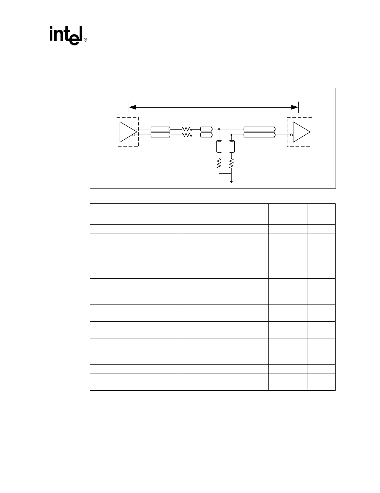
The value of Rt should be 49 Ω, and Rs should be 33 Ω. Simulations have shown that Rs values
above 33 Ω provide no benefit to signal integrity but only degrade the edge rate.
Figure 4-14. Source Shunt Termination
Platform Clock Routing Guidelines
LT = L1 + L2 + L4
L1
L1'
Clock
Driver
Table 4-9. SCR/SCR# Routing Guidelines
Layout Guideline Value Illustration Notes
Trace Width 5 mil Figure 4-15
Differential Pair Spacing 11 mils Figure 4-15 1,2,3
Spacing to Other Traces 25 mils Figure 4-15
Serpentine Spacing
Motherboard Impedance – Differential 100
Routing Length –
L1, L1’: Clock Driver to Rs
Routing Length –
L2, L2’: Rs to Rs-Rt Node
Routing Length –
L3, L3’: Rs-Rt Node to Rt
Routing Length –
L4, L4’: Rs-Rt Node to Load
SCR – SCR# Length Matching ± 10 mils
Rs Series Termination Value 33
Rt Shunt Termination Value
Rs
Rs
Maintain a minimum 25 mils.
Keep parallel serpentine sections as
short as possible.
Minimize 90-degree bends. Make
45-degree bends, if possible.
L2
L2'
L3
Rt Rt
L3'
L4
L4'
Intel
®
ICH5
Ω typical 4
0.5 inch max Figure 4-14 6,7
0 – 0.2 inch Figure 4-14 6,7
0 – 0.2 inch Figure 4-14 6,7
2 – 15 inches Figure 4-14
Ω ± 5% Figure 4-14
49.9
Ω± 1%
Ω odd mode MB impedance)
(for 50
Figure 4-14 5
NOTES:
1. Edge-to-edge spacing between the two traces of any differential pair. Uniform spacing should be maintained
along the entire length of the trace.
2. Clock traces are routed in a differential configuration. Maintain the minimum recommended spacing between
the two traces of the pair. Do not exceed the maximum trace spacing, as this will degrade the noise rejection
of the network
Intel® 875P Chipset Platform Design Guide 57

Platform Clock Routing Guidelines
3. Set line width to meet correct motherboard impedance. The line width value provided here is a
recommendation to meet the proper trace impedance based on the recommended stack up.
4. The differential impedance of each clock pair is approximately 2*Zsingle-ended*(1–2*Kb) where Kb is the
backwards cross-talk coefficient. For the recommended trace spacing, Kb is very small, and the effective
differential impedance is approximately equal to 2 times the single-ended impedance of each half of the pair.
5. Rt shunt termination value should match the motherboard impedance.
6. Minimize L1, L2, and L3 lengths. Long lengths on L2 and L3 degrade effectiveness of source termination and
contribute to ringback.
7. The goal of constraining all bus clocks to one physical routing layer is to minimize the impact on skew due to
variations in Er and the impedance variations due to physical tolerances of circuit board material.
Figure 4-15. Trace Spacing for SRC Clocks
S1
WW
SRC SRC#
h
S
S1
Ground Plane
4.2.6.2 SRC General Routing Guidelines
• When routing the 100-MHz differential clocks, do not split up the two halves of a differential
clock pair between layers, and route to all agents on the same physical routing layer referenced
to ground.
• If a layer transition is required, make sure skew induced by the vias used to transition between
routing layers is compensated in the traces to other agents.
• Do not place vias between adjacent complementary clock traces, and avoid differential vias.
Vias placed in one half of a differential pair must be matched by a via in the other half.
Differential vias can be placed within length L1, between clock driver and Rs, if needed to
shorten length L1.
58 Intel
®
875P Chipset Platform Design Guide

4.3 Clock Driver Decoupling
• For all power connection to planes, decoupling capacitors and vias, the maximum trace width
allowable and shortest possible lengths should be used to ensure lowest possible inductance.
• The VSS pins should not be connected directly to the VSS side of the capacitors. They should
be connected to the ground flood under the part which is viaed to the ground plane to avoid
VDD glitches propagating out, getting coupled through the decoupling capacitors to the VSS
pins. This method has been shown to provide the best clock performance.
• The ground flood should be viaed through the ground plane with no less than 12–16 vias under
the part. It should be well connected.
• For all power connections, heavy duty and/or dual vias should be used.
• It is imperative that the standard signal vias and small traces not be used for connecting
decoupling capacitors and ground floods to the power or ground planes.
4.3.1 CK409 Power Plane Filtering
4.3.1.1 VDD Plane Filtering
Platform Clock Routing Guidelines
The VDD decoupling requirements for a CK409 compliant clock synthesizer are as follows:
• One, 300 Ω (100 MHz) Ferrite Bead is recommended for the VDD plane
• A 10 µF bulk decoupling capacitor placed near the clock chip is recommended for the VDD
plane. Two, 4.7 µF capacitors can also be used in place of the 10 µF capacitor.
• Seven, 0.1 µF high-frequency decoupling capacitors should be placed as close to each VDD
pin as possible.
4.3.1.2 VDDA Plane Filtering
The VDDA decoupling requirements for a CK409 compliant clock synthesizer are as follows:
• One, 300 Ω (100 MHz) Ferrite Bead is recommended for the VDDA plane
• A 10 µF bulk decoupling capacitor placed near the clock chip is recommended for the VDDA
plane. Two, 4.7 µF capacitors can also be used in place of the 10 µF capacitor.
• One, 0.1 µF high-frequency decoupling capacitor should be placed as close to each VDDA pin
as possible.
4.3.1.3 VDD_48 Plane Filtering
The VDD _48 decoupling requirements for a CK409 compliant clock synthesizer are as follows:
• One, 5Ω series resistor is recommended for the VDD _48 plane
• One, 4.7 µF bulk decoupling capacitor placed near the VDD _48 pin is recommended for the
VDD _48 plane.
• One, 0.1 µF high-frequency decoupling capacitor should be placed as close to the VDD_48 pin
as possible.
Intel® 875P Chipset Platform Design Guide 59

Platform Clock Routing Guidelines
.
Figure 4-16. Decoupling Capacitors Placement and Connectivity
VDD_48
VDD_48
.1uf
.1uf
FB
Decoupling
Decoupling
FB
10uF
10uF
VDD
VDD
4.7uF
4.7uF
.1uf
.1uf
10uF
10uF
.1uf
.1uf
FB
FB
VDD_A
VDD_A
Caps
Caps
4.4 EMI Constraints
Clocks are a significant contributor to EMI. The following recommendations can aid in EMI
reduction:
GND
GND
Decoupling
Decoupling
Caps
Caps
• Maintain uniform spacing between the two halves of differential clocks.
• Route clocks on physical layer adjacent to the VSS reference plane only.
60 Intel
®
875P Chipset Platform Design Guide

Front Side Bus (FSB)
Front Side Bus (FSB) 5
5.1 General Topologies and Layout Guidelines
This section covers the Front Side Bus source synchronous (data, address, and associated strobes)
and common clock signal routing for the Pentium 4 processor on 0.13 micron process and the Intel
Pentium 4 processor on 90 nm process in an 875P chipset-based platform. Ta ble 5-1 lists the
signals and their corresponding signal types.
Table 5-1. System Bus Signal Groups
Signal Group Type Signals
AGTL+ Common
Clock Input
AGTL+ Common
Clock I/O
AGTL+ Source
Synchronous I/O
Synchronous to
BCLK[1:0]
Synchronous to
BCLK[1:0]
Synchronous to
assoc. strobe
BPRI#, DEFER#, RESET#
AP[1:0]#, ADS#, BINIT#, BNR#, BPM[5:0]#
DP[3:0]#, DRDY#, HIT#, HITM#, LOCK#, MCERR#
Signals Associated Strobe
REQ[4:0]#, A[16:3]#4ADSTB0#
A[35:17]#
D[15:0]#, DBI0# DSTBP0#, DSTBN0#
D[31:16]#, DBI1# DSTBP1#, DSTBN1#
D[47:32]#, DBI2# DSTBP2#, DSTBN2#
D[63:48]#, DBI3# DSTBP3#, DSTBN3#
4
3, 5
ADSTB1#
1
, RS[2:0]#, RSP#, TRDY#
3, 5
, BR0#3, DBSY#,
AGTL+ Strobes
Asynchronous
GTL + I nput
Asynchronous
GTL+ Output
Asynchronous
GTL+ Input/Output
TAP Input
TAP Output
System Bus Clock Clock BCLK[1:0], ITP_CLK[1:0]
Power/Other
NOTES:
1. Refer to the processor datasheet for signal descriptions.
2. In processor systems where there is no debug port implemented on the system board, these signals are used
to support a debug port interposer. In systems with the debug port implemented on the system board, these
signals are no connects.
3. These signal groups are not terminated by the processor. Refer to the processor debug port design guide,
and Section 5.1.6 for termination requirements and further details.
4. The value of these pins during the active-to-inactive edge of RESET# defines the processor configuration
options. See the processor datasheet for details.
5. These signals do not have R
3
3
3
3
Synchronous to
BCLK[1:0]
Synchronous to TCK TCK, TDI, TMS, TRST#
Synchronous to TCK TDO
termination on die.
L
ADSTB[1:0]#, DSTBP[3:0]#, DSTBN[3:0]#
A20M#, IGNNE#, INIT#, LINT0/INTR, LINT1/NMI, SMI#, SLP#,
STPCLK#
FERR#, IERR#, THERMTRIP#
PROCHOT#
5
VCC, VCCA, VCCIOPLL, VID[5:0], VSS, VSSA, GTLREF[3:0],
COMP[1:0], RESERVED, TESTHI[12:0], THERMDA,
THERMDC, VCC_SENSE, VSS_SENSE, VCCVID, VCCVIDLB,
BSEL[1:0], SKTOCC#, DBR#
OPTIMIZED/COMPAT#
process signal), IMPSEL
process signal), PWRGOOD
5
2
2
, VIDPWRGD, BOOTSELECT,
3
(Intel Pentium 4 processor on 90 nm
3
(Pentium 4 processor on 0.13 micron
3, 5
Intel® 875P Chipset Platform Design Guide 61

Front Side Bus (FSB)
5.1.1 Trace Spacing Rules
The spacing rules are based upon board stack-up and dielectric thickness, not on trace width. A 3:1
spacing rule corresponds to the air gap (distance S) between traces must be 3X the distance from
the trace to the ground plane(distance h). For instance, if the dielectric thickness was 4.1 mils, and
the trace space guidelines calls for 3:1 spacing, the air gap between traces must be 12.3 mils.
Figure 5-1. Spacing Diagram
W
Trace A
Trace B Trace C
h
Ground Plane
5.1.2 Signal Groups
This section covers the AGTL+ system bus 1X, 2X, and 4X signals as well as their associated
strobe pairs.
Table 5-2. 1X, 2X and 4X Signal Groups
1X 2X Group 4X Group
BPRI#,DEFER#,RS[2:0]#,
TRDY#,ADS#,BNR#,DBSY,DRDY#,
HIT#,HITM#,LOCK#
Table 5-3. Address and Data, and Associated Strobe Pairs
Data/Address Group Associated Strobes
A[31:3]#, REQ[4:0]#,
ADSTB[1:0]#
WW
S
SS
D[63:0]#, DSTBP[3:0]#,
DSTBN[3:0]#,DBI[3:0]#
W
Trace D
D[63:48]#, DBI3# DSTBP3#, DSTBN3#
D[47:32]#, DBI2# DSTBP2#, DSTBN2#
D[31:16]#, DBI1# DSTBP1#, DSTBN1#
D[15:0]#, DBI0# DSTBP0#, DSTBN0#
A[31:17]# ASTB1#
A[16:3]#, REQ[4:0]# ASTB0#
62 Intel
®
875P Chipset Platform Design Guide

5.1.3 Motherboard Layout Rules for AGTL+ Signals
The following topologies and layout guidelines are preliminary and are subject to change. These
guidelines are derived from simulations with the processor and 875P chipset package models. All
lengths are pin-to-pin lengths, but length matching must be pad-to-pad.
5.1.3.1 4X Routing Guidelines
Table 5-4. 4X Routing Guidelines
Signal Name Spacing Length Referencing Topology Impedance Matching Notes
D[63:0]# 3:1 2.5” to 6” VSS 1 60 Ω ± 15% ± 25 mils 2,3,4,5
DSTBP[3:0]# 4:1 2.5” to 6” VSS 1 60
DSTBN[3:0]# 4:1 2.5” to 6” VSS 1 60
DBI[3:0]# 3:1 2.5” to 6” VSS 1 60
NOTE:
1. DSTBP[3:0]# and DSTBN[3:0]# must not be routed adjacent to each other and have 4:1 spacing.
2. All signal groups within the 4X data group must be routed on the same layer.
3. Length matching must include motherboard compensation for MCH and processor package trace lengths.
4. Strobe length matching: Length_DSTBPx = Length_DSTBNx ± 25 mils.
5. Data to strobe length matching: Length_data = (Length_DSTBPx + Length_DSTBNx)/2 ± 25.
Ω ± 15% ± 25 mils 1,2,3,4
Ω ± 15% ± 25 mils 1,2,3,4
Ω ± 15% ± 25 mils 2,3,5
Front Side Bus (FSB)
5.1.3.2 2X Routing Guidelines
Table 5-5. 2X Routing Guidelines
Signal Name Spacing Length Referencing Topology Impedance Matching Notes
A[31:3]# 3:1 3” to 10” VSS 1 60 Ω ± 15% ± 100 mils 2,3
ADSTB[1:0]# 4:1 3” to 10” VSS 1 60
REQ[4:0]# 3:1 3” to 10” VSS 1 60
NOTE:
1. ADSTB[1:0]# need to be routed 4:1 from everything.
2. Length matching must include motherboard compensation for package trace lengths.
3. Address to strobe length matching: Length_address = Length_ADSTB ± 100.
4. To ensure clean breakout and routing from the MCH-to-processor for the signal groups in Ta b l e 5 - 5, these
signals are allowed to transition layers and route for up to 750 mils maximum length, at which point the signal
must transition back to the original layer or connect to the MCH or processor pin.
4
Ω ± 15% N/A 1,2,3
Ω ± 15% ± 100 mils 2,3
Intel® 875P Chipset Platform Design Guide 63
Front Side Bus (FSB)
5.1.3.3 1X Routing Guidelines
Table 5-6. 1X Routing Guidelines
Signal Name Spacing Length Referencing Topology Impedance Notes
BPRI# 3:1 3” to 8” VSS 1 60 Ω ± 15% 1,2
DEFER# 3:1 3” to 8” VSS 1 60
RS[2:0]# 3:1 3” to 8” VSS 1 60
TRDY# 3:1 3” to 8” VSS 1 60
ADS# 3:1 3” to 8” VSS 1 60
BNR# 3:1 3” to 8” VSS 1 60
DBSY# 3:1 3” to 8” VSS 1 60
DRDY# 3:1 3” to 8” VSS 1 60
HIT# 3:1 3” to 8” VSS 1 60
HITM# 3:1 3” to 8” VSS 1 60
LOCK# 3:1 3” to 8” VSS 1 60
NOTE:
1. 3:1 spacing is the minimum requirement, if 4:1 spacing is achievable, 4:1 spacing is preferred.
2. For routes 7 inches to 8 inches, 4:1 spacing is required.
Ω ± 15% 1,2
Ω ± 15% 1,2
Ω ± 15% 1,2
Ω ± 15% 1,2
Ω ± 15% 1,2
Ω ± 15% 1,2
Ω ± 15% 1,2
Ω ± 15% 1,2
Ω ± 15% 1,2
Ω ± 15% 1,2
5.1.3.4 Ground Referencing
It is strongly recommended that AGTL+ signals be routed on a signal layer that is next to the
ground layer (referenced to ground). It is important to provide effective signal return paths with
low inductance. The best routing is directly adjacent to a solid ground plane with no splits or cuts.
Reference Plane Splits
Splits in reference planes disrupt signal return paths and increase overshoot, undershoot, and ringback due to significantly increased inductance. This is very hard to predict and suppress; thus, such
plane splits under AGTL+ signals should be avoided.
64 Intel
®
875P Chipset Platform Design Guide
Front Side Bus (FSB)
5.1.4 Motherboard Layout Rules for Async AGTL+ Signals
For all Asynchronous AGTL+ signals, routing can be done on any layer or combination of layers.
Table 5- 7 provides insight for routing these signals, but Section 5.1.6 further details the routing
topologies and layout requirements.
Table 5-7. Routing Guidelines for Asynchronous AGTL+ Signals
Signal Impedance Spacing
THERMTRIP# 60 Ω ± 15% 7 mils 5 mils 2
FERR# 60
A20M# 60
IGNNE# 60
SMI# 60
SLP# 60
STPCLK# 60
LINT[1:0] 60
IERR# 60
BR0# 60
RESET# 60
INIT# 60
PWRGOOD 60
PROCHOT# 60
TESTHI 60
COMP[1:0] 60
BOOTSELECT 60
RESERVED NA NA NA 12
OPTIMIZED/COMPAT# (Intel Pentium 4
processor on 90 nm process signal)
IMPSEL
(Pentium 4 processor on 0.13 micron
process signal)
RSP# NA NA NA 13
Ω ± 15% 7 mils 5 mils 2
Ω ± 15% 7 mils 5 mils 3
Ω ± 15% 7 mils 5 mils 3
Ω ± 15% 7 mils 5 mils 3
Ω ± 15% 7 mils 5 mils 3
Ω ± 15% 7 mils 5 mils 3
Ω ± 15% 7 mils 5 mils 3
Ω ± 15% 7 mils 5 mils 4
Ω ± 15% 13 mils 5 mils 5
Ω ± 15% 13 mils 5 mils 5
Ω ± 15% 7 mils 5 mils 6
Ω ± 15% 13 mils 5 mils 7
Ω ± 15% 7 mils 5 mils 8
Ω ± 15% 7 mils 5 mils 9
Ω ± 15% 13 mils 5 mils 10
Ω ± 15% 7 mils 5 mils 11
NA NA NA 13
1
Trace Width Topology
NOTE: 1. Recommend routing INIT# with 7 mils spacing. If 5 mils spacing is used, total length must be less
than 8".
Intel® 875P Chipset Platform Design Guide 65
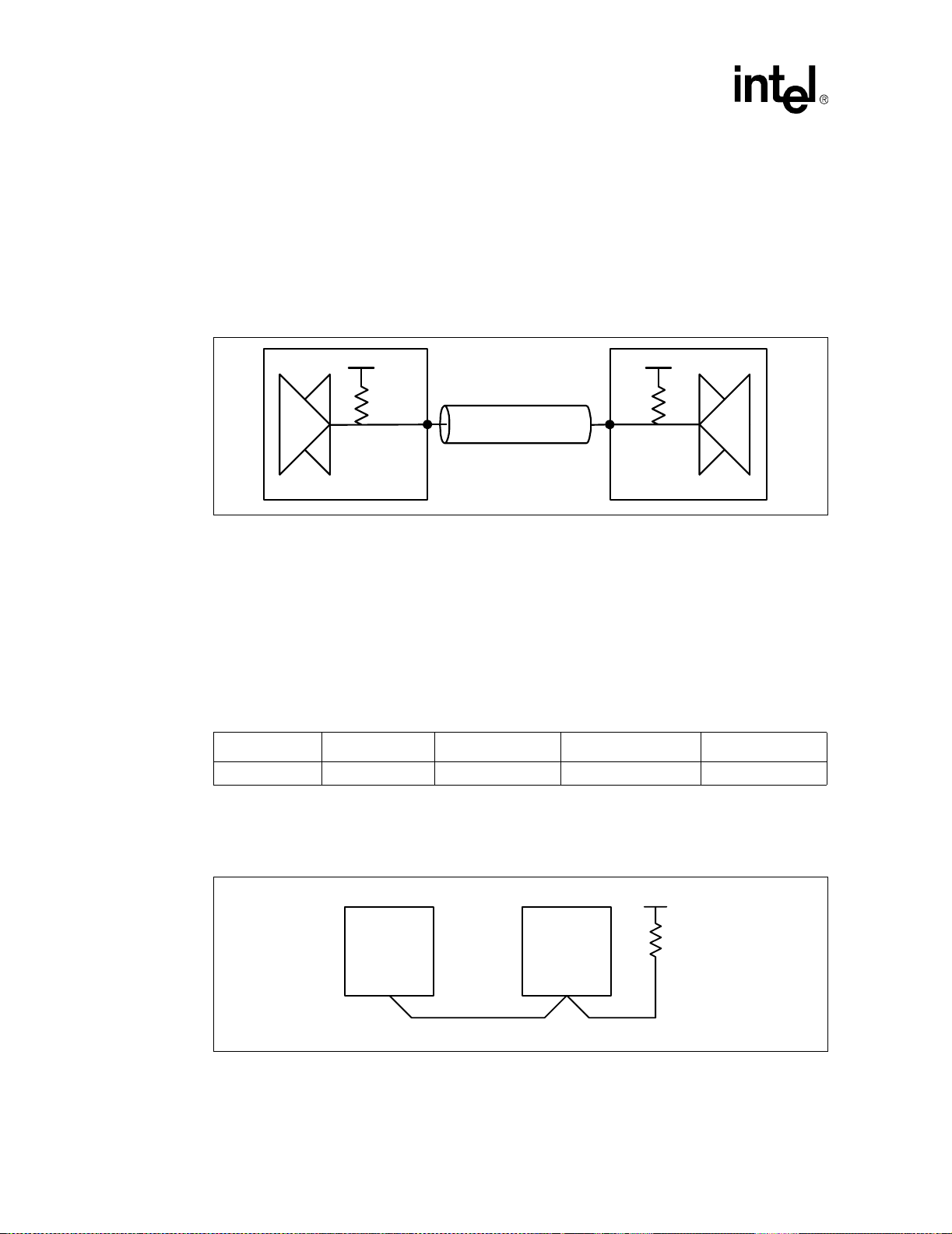
Front Side Bus (FSB)
5.1.5 AGTL+ Layout Topologies
5.1.5.1 Topology 1
Topology 1 requires that the signals be routed directly from the processor to the chipset. Both the
processor and the chipset have on-die termination (ODT), which removes the need for termination
resistors on the motherboard. Thus, the signal is dual-end terminated. The allowable break-in and
breakout region for AGTL+ signals is 500 mils at 5-mil traces with 5-mil separation.
Figure 5-2. Topology 1
Processor
Vcc_CPU
Rtt
L
pkg_cpu
L1
5.1.6 Non AGTL+ Topologies
5.1.6.1 Topology 2: THERMTRIP# and FERR#
These signals adhere to the following routing and layout recommendations. Figure 5-3 illustrates
the recommended topology. If THERMTRIP# is routed to external logic, voltage translation may
be required to avoid excessive voltage levels at the processor and to meet input thresholds for the
external logic.
Table 5-8. Layout Recommendations for FERR# and THERMTRIP#
Trace Z
0
60 Ω ± 15% 7mils 1 inch to 12 inches 3 inches maximum 62 Ω ± 5%
NOTE:
1. THERMTRIP# can be routed next to FERR# with 5-mil spacing for up to 17 inches.
2. THERMTRIP# or FERR# cannot be routed next to any other signal for more than 8 inches at 7-mil spacing.
Trace Spacing L1 L2 Rpu
Vcc_CPU
Rtt
L
pkg_mch
MCH
Figure 5-3. Routing Illustration for FERR# and THERMTRIP#
Processor
Intel
ICH5
L1 L2
66 Intel
VCC_CPU
®
®
875P Chipset Platform Design Guide
Rpu
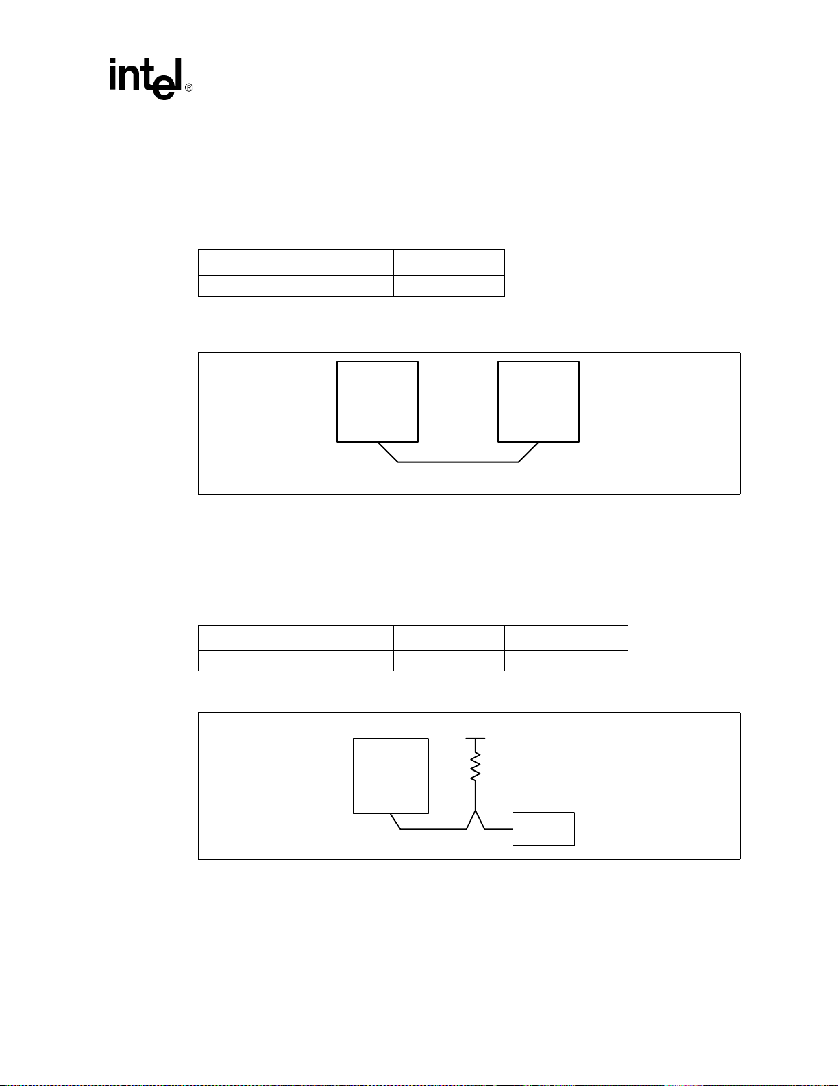
5.1.6.2 Topology 3: A20M#, IGNNE#, SMI#, SLP#, STPCLK#, LINT[1:0]
These signals adhere to the following routing and layout recommendations. Figure 5-4 illustrates
the recommended topology.
Table 5-9. Layout Recommendations for Miscellaneous Signals
Front Side Bus (FSB)
Trace Z
0
60 Ω ± 15% 7 mils 17 inches maximum
Trace Spacing L1
Figure 5-4. Routing Illustration for A20M#, IGNNE#, SMI#, SLP#, STPCLK#,
and LINT[1:0]
®
Processor
Intel
ICH5
L1
5.1.6.3 Topology 4: IERR#
The IERR# signal does not have on-die termination and must be terminated if it is used. If the
signal is not used, it can be left as a no connect. Figure 5-5 illustrates the recommended topology if
the pin is used.
Table 5-10. Layout Recommendations for IERR#
Trace Z
0
60 Ω ± 15% 7 mils 1 inch maximum 62 Ω ± 5%
Trace Spacing L1 Rpu
Figure 5-5. Routing Illustration for IERR
VCC_CPU
Processor
L1
Intel® 875P Chipset Platform Design Guide 67
Rpu
External
Logic
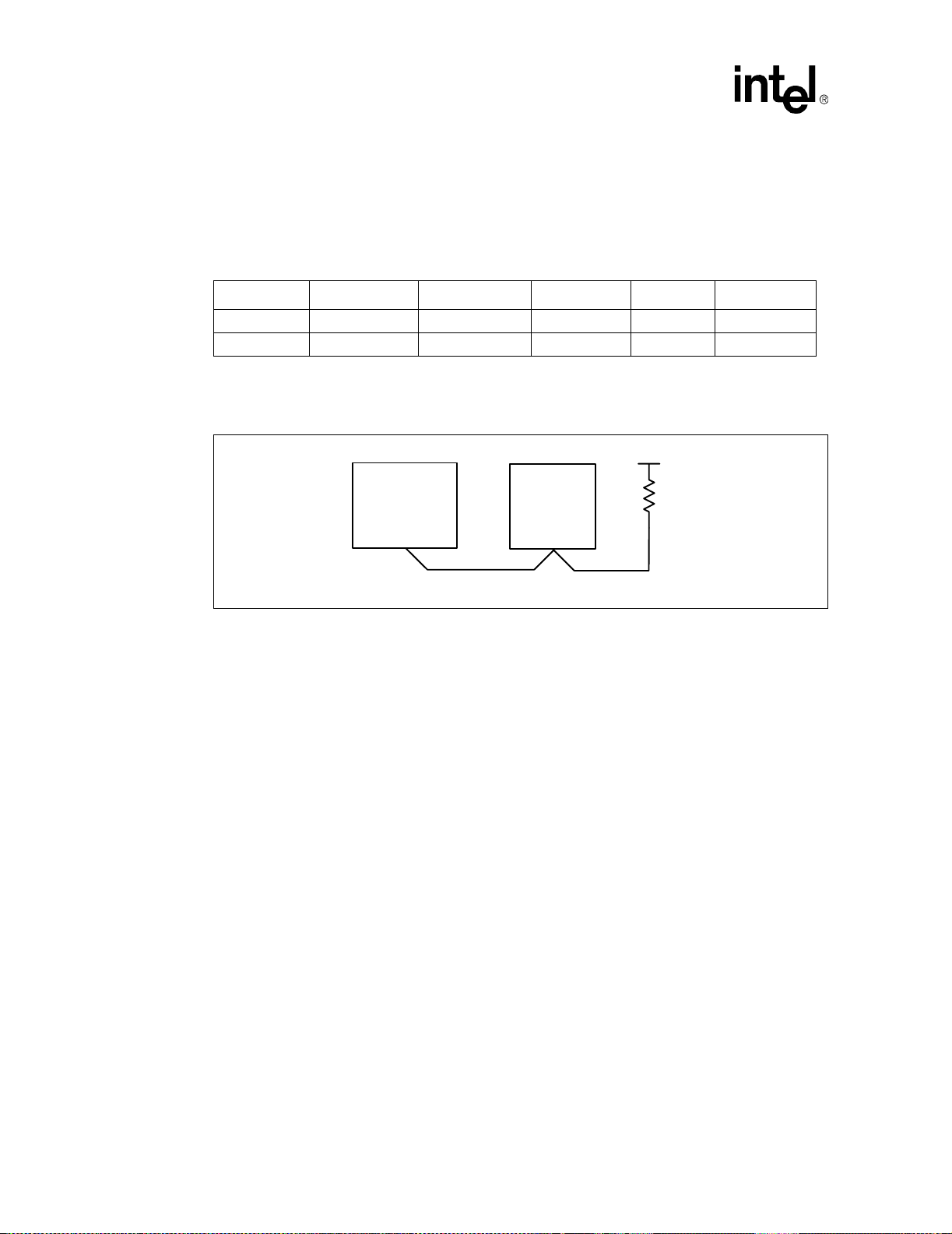
Front Side Bus (FSB)
5.1.6.4 Topology 5: RESET# and BR0#
Since the processor does not have on-die termination on the RESET# or BR0# signals, it is
necessary to terminate them using discrete components on the system board. Connect the signals
between the MCH and the processor, as shown in Figure 5-6.
Table 5-11. Layout Recommendations for RESET# and BR0#
Pin Name Trace Z
RESET# 60 Ω ± 15% 13 mils 2” to 10” 1” to 2” 62 Ω ± 5%
BR0# 60
NOTES:
1. BR0# can be routed with 7-mil spacing for up to 8 inches.
0
Ω ± 15% 13 mils 2” to 10” 1” to 2” 200 Ω ±5%
Trace Spacing L1 L2 Rpu
Figure 5-6. Routing Illustration for RESET# and BR0#
MCH
L1
Processor
VCC_CPU
Rpu
L2
68 Intel
®
875P Chipset Platform Design Guide
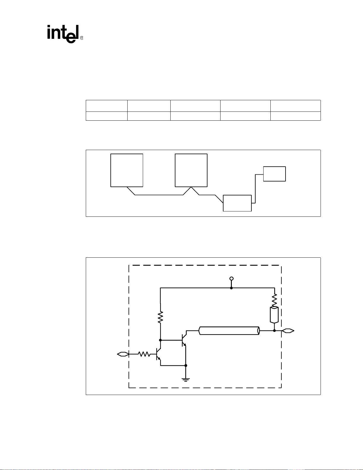
5.1.6.5 Topology 6: INIT#
The INIT# signal adheres to the following routing and layout recommendations. Figure 5-7
illustrates the recommended topology.
Table 5-12. Layout Recommendations For INIT#
Trace Z
0
60 Ω ± 15% 7 mils 17 inches maximum 2 inches maximum 10 inches maximum
NOTE: 1. Recommend routing INIT# with 7 mils spacing. If 5 mils spacing is used, total length must be less
than 8".
Figure 5-7. INIT# Topology
Trace Spacing
1
Front Side Bus (FSB)
L1 L2 L3
Processor
L1 L2
NOTE: External logic is represented by Figure 5-8.
Level shifting is required for the INIT# signals to the flash BIOS to meet the input logic levels of
the flash BIOS. Figure 5-8, illustrates one method of implementing this item.
Figure 5-8. Voltage Translation of INIT#
2.2 kΩ
± 5%
From_Driver
3904
330 Ω
± 5%
Intel® ICH5
3904
FLASH
BIOS
L3
Voltage
Translator
Vcc_of_Receiver
330 Ω
± 5%
T2
To_Receiver
T1
T1 = 10" max
T2 = 3" max
Intel® 875P Chipset Platform Design Guide 69
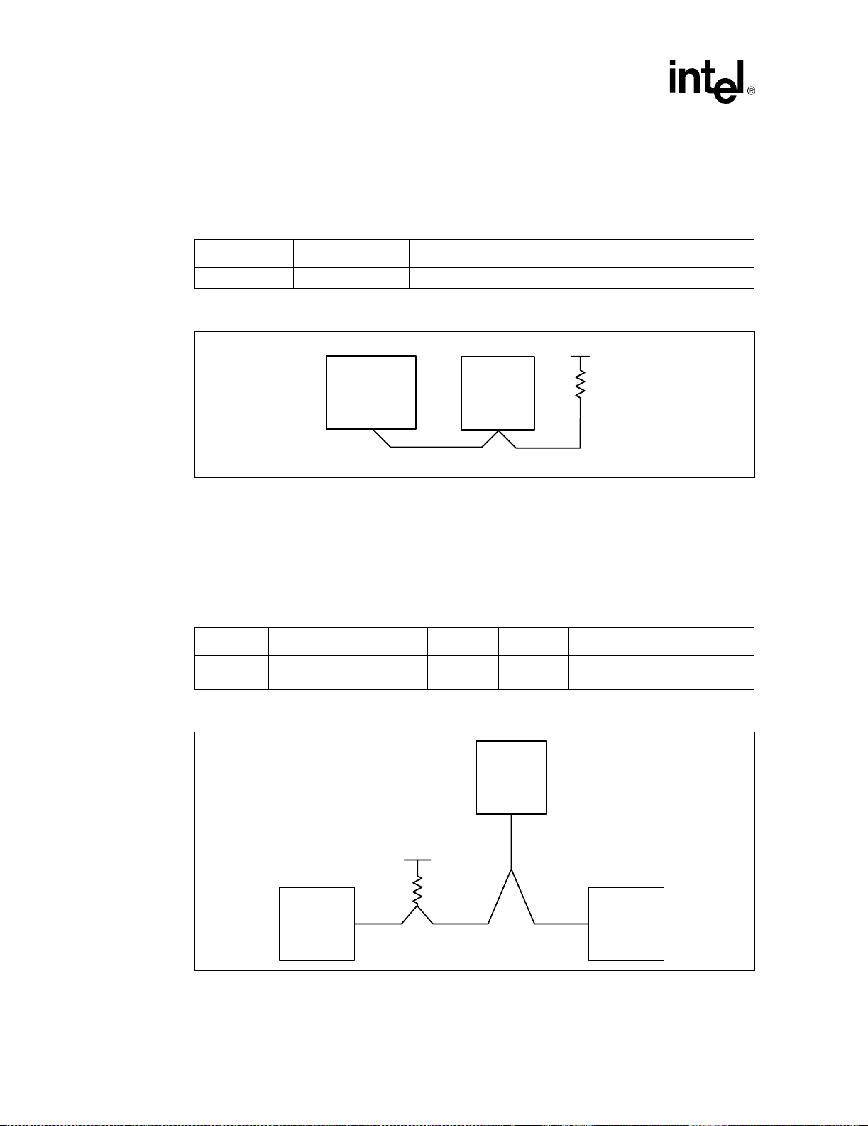
Front Side Bus (FSB)
5.1.6.6 Topology 7: PWRGOOD
The PWRGOOD signal adheres to the following routing and layout recommendations. Figure 5-9
illustrates the recommended topology.
Table 5-13. Layout Recommendations for PWRGOOD
Trace Z
0
60 Ω ± 15% 13 mils 1 inch to 12 inches 3 inches maximum 300 Ω ± 5%
Trace Spacing L1 L2 Rpu
Figure 5-9. Routing Illustration for PWRGOOD
Intel® ICH5
5.1.6.7 Topology 8: PROCHOT#
PROCHOT# adheres to the following routing and layout recommendations. Figure 5-10 illustrates
the recommended topology. If PROCHOT# is routed to external logic, voltage translation may be
required to avoid excessive voltage levels at the processor and to meet input thresholds for external
logic.
Table 5-14. Layout Recommendations for PROCHOT#
Trace Z0Trace Spacing L1 L2 L3 L4 Rpu
60 Ω ± 15% 7 mils
0.75 inch
maximum
L1
10 inches
maximum
Processor
10 inches
maximum
L2
VCCP
0.5 inch
maximum
Rpu
120 Ω –140 Ω ± 5%
Figure 5-10. Routing Illustration for PROCHOT#
VRD
10.0
VCCP
Rpu
Processor MCH
L1
L2 L3
70 Intel
L4
®
875P Chipset Platform Design Guide
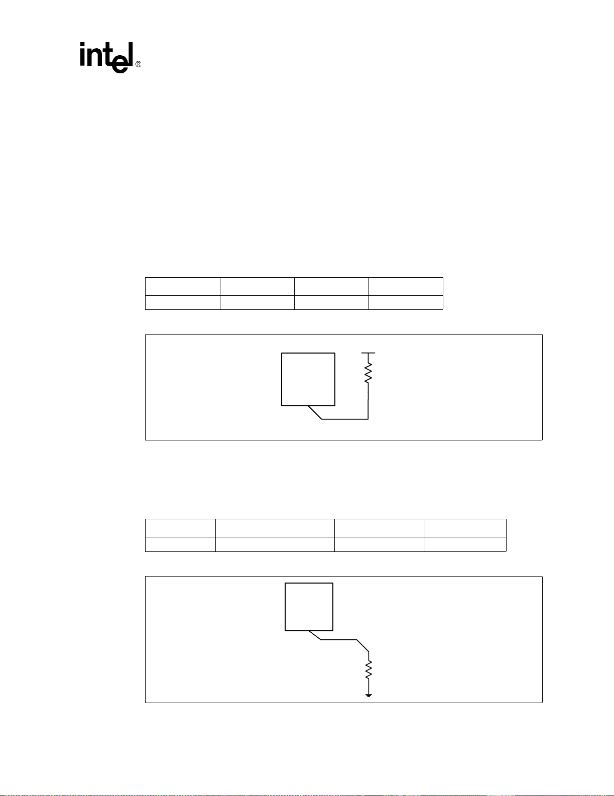
5.1.6.8 Topology 9: TESTHI Signals
The TESTHI pins adhere to the following routing and layout recommendations. Figure 5-11
illustrates the recommended topology. The TESTHI pins may use individual pull-up resistors, or be
grouped together as detailed below. A matched resistor, Rpu, should be used for each group.
• TESTHI[1:0]
• TESTHI[7:2]
• TESTHI8 - Cannot be grouped with any other TESTHI signal
• TESTHI9 - Cannot be grouped with any other TESTHI signal
• TESTHI10 - Cannot be grouped with any other TESTHI signal
• TESTHI11 - Cannot be grouped with any other TESTHI signal
• TESTHI12 - Cannot be grouped with any other TESTHI signal
Table 5-15. Layout Recommendations for TESTHI Signals
Front Side Bus (FSB)
Trace Z
0
60 Ω ± 15% 7 mils 1 inch maximum 62 Ω ± 5%
Trace Spacing L1 Rpu
Figure 5-11. Routing Illustration for TESTHI and Signals
Processor
5.1.6.9 Topology 10: COMP[1:0]
The COMP[1:0] signals adhere to the following routing and layout recommendations. Figure 5-12
illustrates the recommended topology.
Table 5-16. Layout Recommendations for COMP[1:0]
Trace Z
0
60 Ω ± 15% 13 mils 1.5 inches maximum 61.9 Ω ± 1%
Figure 5-12. Routing Illustration for COMP[1:0]
Trace Spacing L1 Rpd
VCC_CPU
Rpu
L1
Processor
L1
Rpd
Intel® 875P Chipset Platform Design Guide 71
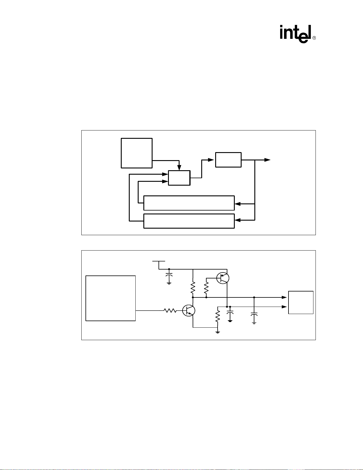
Front Side Bus (FSB)
5.1.6.10 Topology 11: BOOTSELECT
The Intel Pentium 4 processor on 90 nm process and Pentium 4 processor on 0.13 micron process
loadlines require a different slope. Therefore, the VRD must switch feedback networks depending
on which processor is installed. The BOOTSELECT signal is used by the VRD to detect whether
an Intel Pentium 4 processor on 90 nm process or Pentium 4 processor on 0.13 micron process is
inserted into the processor socket and switches the feedback network. Figure 5-13 illustrates the
switching while Figure 5-14 shows an example switching circuit. Refer to the appropriate
;
Figure 5-13. VRD Feedback Switching Diagram
processor datasheet for the specifications for each processor
Processor
Bootselect
Switch
Inte l® Pentium® 4 processor on
0.13 micron process FB Network
Inte l® Pentium® 4 processor on
90 nm process FB Network
Figure 5-14. Routing Illustration for BOOTSELECT
5VSB
0.1 µF
2.7 kΩΩΩΩ
Processor
BOOTSELEC T
12 kΩΩΩΩ
VRD 10.0 Controller
FB OUT
10 kΩΩΩΩ
10 kΩΩΩΩ
0.1 µF
NW_HI
PSC_HI
0.1 µF
VRD
10.0
5.1.6.11 Topology 12: RESERVED
All RESERVED pins must remain unconnected. Connection of these pins to VCC, VSS, or any
other signal (including each other) can result in component malfunction or incompatibility with a
future processor.
72 Intel
®
875P Chipset Platform Design Guide
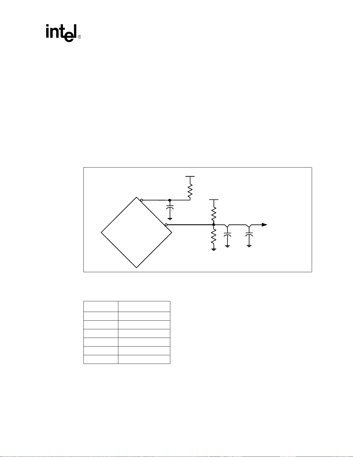
5.1.6.12 Topology 13: OPTIMIZED/COMPAT# or IMPSEL
For the Intel Pentium 4 processor on 90 nm process, the OPTIMIZED/COMPAT# pin on the
processor socket should be left as a no connect (NC).
For the Pentium 4 processor with 512-KB L2 cache on 0.13 micron process, the IMPSEL pin on
the processor socket should be left as a no connect (NC).
5.1.6.13 Host VREFs
The AGTL+ VREF provides a reference voltage for all of the Front Side Bus signals on the
processor and MCH. It is required that a voltage divider yields 0.63 *VCC_AVG where
VCC_AVG is the average voltage of VCC (processor core) and MCH_VTT. The output is then
routed to the processor’s GTLREF and to the MCH’s HDVREF pin. The trace should be a
minimum of 12-mils wide and have a minimum of 15-mils separation from any other trace.
Figure 5-15. HD_VREF Circuit Topology
MCH_VTT
R1
L3
VCC_CPU
R2
L4
R3
PIN A7
HDVREF1
L1
PIN F15
HDVREF0
L2
C1
MCH
C2
Front Side Bus (FSB)
L5
L6
C3
CPU GTLREF
PIN
NOTE: The MCH pins A7 and F15 are tied together in the package. This enables the two HDVREF pins to
share a portion of the divider circuits, pull-down resistor R3.
Table 5-17. Host VREF Resistor Values
Resistor Value
R1 200 Ω ± 1%
R2 200 Ω ± 1%
R3 169 Ω ± 1%
1
C1
C2 0.1 or 1.0 µF
2
C3
NOTE:
1. C1 should be placed as close to the MCH pin as possible
2. C3 should be placed as close to the processor pin as possible.
Intel® 875P Chipset Platform Design Guide 73
0.1 µF or 220 pF
220 pF

Front Side Bus (FSB)
Table 5-18. Host VREF Trace Lengths
Segment Value
L1+L2 3.5 inches maximum
L3 3 inches maximum
L4+L5+L6 1.5 inches maximum
5.1.6.14 Host VID Topology
The host VID signals are used to set the VCC (processor core) voltages. These signals are open
drain and require pull-up resistors. The resistors should be 1 kΩ
For the VID code to arrive at the VRD, System Management Controller, and SIO with good signal
integrity, it is required that the VID topology be as shown in Figure 5-16. Note that it is not
required to route each leg of the diagram. For instance, if you only needed to route the VID lines
from the processor to the voltage regulator, you do not need to route legs L3 and L4. If the
following topology cannot be followed, then it is recommended that thorough simulation be done
to guarantee good signal integrity. The pull-up resistors can be located anywhere in the topology.
Figure 5-16. VID Topology
± 5% and pulled up to 3.3 V.
Processor VRD 10.0
System
Management
Table 5-19. VID Topology Trace Lengths
Dimension Min Max Units
L1 — 12 Inches
L2 — — Inches
L1+L2+L5 — 15 Inches
L3 — 6 Inches
L4 — 6 Inches
L5 — 12 Inches
L1
L3 L4
L2
L5
SIO
74 Intel
®
875P Chipset Platform Design Guide

5.1.6.15 THERMDA/THERMDC
The processor incorporates an on-die thermal diode. THERMDA (diode anode) and THERMDC
(diode cathode) pins on the processor can be connected to a thermal sensor located on the system
board to monitor the die temperature of the processor for thermal management/long term die
temperature change monitoring purpose. This thermal diode is separate from the Thermal
Monitor’s thermal sensor and cannot be used to predict the behavior of the Thermal Monitor.
Because the thermal diode is used to measure a very small voltage from the remote sensor, care
must be taken to minimize noise induced at the sensor inputs. Below are some guidelines:
• Remote sensor should be placed as close as possible to the THERMDA/THERMDC pins. It
can be approximately 4 to 8 inches away as long as the worst noise sources such as clock
generators, data buses and address buses, etc., are avoided.
• Route the THERMDA/THERMDC lines in parallel and close together with ground guards
enclosing the them.
• Use wide traces to reduce inductance and noise pickup that may be introduced by narrow
traces or the system. A width of 10 mils and spacing of 10 mils is recommended.
5.1.6.16 Host RCOMP
The RCOMP pins are used to calibrate the AGTL+ buffers and need to be terminated to a
20 Ω
± 1% pull-down resistor. It is recommended that the trace be a maximum of 0.5-inch long and
be a minimum of 10-mils wide to reduce trace inductance. Keep this trace a minimum of 7 mils
away from other traces.
Front Side Bus (FSB)
5.1.6.17 Host SWING
VSWING needs to be 1/4*MCH_VTT, so a resistor divider with a 301 Ω ±1% pull-up and a
±1% pull-down are recommended. The HXSWING and HYSWING can be tied together on
102 Ω
the motherboard to reduce redundant circuitry. Decouple with one 0.01 µF capacitor at the MCH.
The trace to the MCH should be routed at a maximum of 3 inches long at 12-mils wide and 10-mil
spacing. This can be accomplished on Layer 2 (see Figure 5-17).
Figure 5-17. Host SWING Routing Example
HD_SWING
H_GTLREF_MCH
Intel® 875P Chipset Platform Design Guide 75

Front Side Bus (FSB)
5.1.6.18 BSEL
The BSEL circuit determines the FSB frequency. Connect the processor’s BSEL0 signal to the
CK409’s FSA pin. There should be a pull-up resistor and two pull-down resistors whose values are
listed in Tab le 5-20. The middle of the voltage divider circuit should then connect to the MCH’s
BSEL0 pin. The two pull-down resistors form a voltage divider and are required for proper voltage
levels for the MCH. Connect the MCH’s BSEL1 to the CK409 FSB pin in the same manner.
Figure 5-18. BSEL Topology
Processor
BSEL1
BSEL0
Vcc3_CLK=3.3V
R1
R2
R3 R4
R5
CK409
FS_B
FS_A
MCH
BSEL1
BSEL0
R6
Table 5-20. BSEL Resistor Values
Resistor Value
R1 1 kΩ ± 1%
R2 1 kΩ ± 1%
R3 2 kΩ ± 1%
R4 2 kΩ ± 1%
R5 2.49 kΩ ± 1%
R6 2.49 kΩ ± 1%
Table 5-21. FSB Frequency Selection
FSA, FSB FSB Frequency
0,0 400 MHz
1,0 533 MHz
0,1 800 MHz
NOTE: Refer to the processor datasheet for FSA and FSB input latching.
76 Intel
®
875P Chipset Platform Design Guide

5.2 Trace Length Matching
Trace length matching is required within each source synchronous group to compensate for the
package trace length differences between data signals and the associated strobe. This will balance
the strobe-to-signal skew in the middle of the setup and hold window. An example of trace length
matching is given in Example 5-1 on page 5-78.
Trace length matching consists of matching the pad-to-pad lengths for every signal within a signal
group (e.g., HA[35:17]# and ADSTB1#). A pad-to-pad length is measured as follows:
Front Side Bus (FSB)
CPU
-to-MCH
pad
Length = CPU
pad
pkg_len
+ CPU
Where:
CPU
-to-MCH
pin
= Motherboard trace length between processor 1 and MCH.
pin
pkg_len = Pad to pin length within the package.
Contact your Intel representative for information about the Length Matching Spreadsheet tool.
Figure 5-19. Trace Length Matching for the Front Side Bus
CPU
to MCH
pin
Processor MCH
Si
DIE
CPU
pkg_len
Package
When length matching, the board designer should set every signal’s pad-to-pad length equal to
each other, within ± 25 mils. This yields the following equation:
CPU
(Signal 2) + CPU
(Signal 1) + CPU
pkg_len
pin_len
pin_len
to MCH
to MCH
(Signal 2) + MCH
pin_len
(Signal 1) + MCH
pin_len
-to-MCH
pin
pin
pkg_len
+ MCH
pin
MCH
pkg_len
pkg_len
(Signal 2)
pkg_len
Si
DIE
Package
(Signal 1) = CPU
pkg_len
To length match Signal 1 and Signal 2, hold one of the signals constant, and vary the second signal
until the equation is satisfied. Since all the pkg_len values are constant, we can solve for Signal 2:
CPU
MCH
to MCH
pin_len
(Signal 1) – (CPU
pkg_len
(Signal 2) = CPU
pin_len
(Signal 2) + MCH
pkg_len
(Signal 1)+CPU
pkg_len
pkg_len
pin_len
(Signal 2))
to MCH
pin_len
(Signal1) +
Generally, when length matching a group of signals, a designer will first layout all signals to the
shortest length possible allowed by specification. Then, keeping the longest signal as the constant
value (Signal 1), lengthen all the other signals so that the pad-to-pad lengths are all equal.
Intel® 875P Chipset Platform Design Guide 77

Front Side Bus (FSB)
Example 5-1. Trace Length Matching
Consider the signals D4# and DSTBP0# and DSTBN0#, from the same group. Calculate processorto-MCH length for D4#:
CPU
CPU
CPU
CPU
MCH
MCH
CPU
CPU
CPU
CPU
MCH
CPU
+ MCH
(DSTBP0#) = 0.190 inch
pkg_len
(DSTBN0#) = 0.180 inch
pkg_len
to MCH
pin_len
to MCH
pin_len
(DSTBP0#) = 0.240 inch
pkg_len
(DSTBN0#) = 0.250 inch
pkg_len
-to-MCH
pad
-to-MCH
pad
-to-MCH
pad
(D4#) = 0.198 inch
pkg_len
(D4#) = 0.225 inch
pkg_len
toMCH
pin_len
pkg_len
pin_len
pin_len
Length(DSTBP0#) = 5.43 inches
pad
Length(DSTBN0#) = 5.53 inches
pad
Length(DSTBavg) = 5.48 inches
pad
pin_len
(D4#))
(DSTBP0#) = 5.0 inches
(DSTBN0#) = 5.1 inches
(D4#) =CPU
-to-MCH
pad
Length(DSTBavg) – (CPU
pad
pkg_len
(D4#)
Therefore, the PCB trace length of D4# must be within ± 25 mils of 5.057 inches from the
processor to MCH.
5.3 Retention Mechanism Placement and Keep-Outs
The retention mechanism requires a keep-out zone, for limited component height area under the
retention mechanism as shown in Figure 5-20 and Figure 5-21. These figures show the relationship
between the retention mechanism mounting holes and pin one of the socket. In addition, they also
document the keep-outs. For heatsink volumetric information, refer to the processor Thermal
Design Guide.
78 Intel
®
875P Chipset Platform Design Guide

Figure 5-20. Retention Mechanism Keep-Out Drawing 1
Front Side Bus (FSB)
Note:
Dimensions are in millimeters with English dimensions in brackets.
Note:
Dimensions are in millimeters with English dimensions in brackets.
Intel® 875P Chipset Platform Design Guide 79
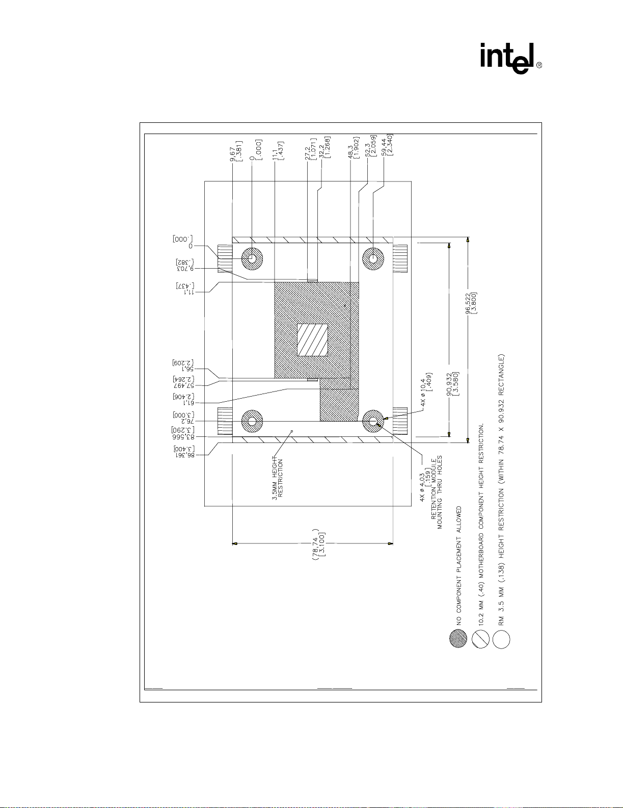
Front Side Bus (FSB)
Figure 5-21. Retention Mechanism Keep-Out Drawing 2
80 Intel
®
875P Chipset Platform Design Guide
Note:
Dimensions are in millimeters with English dimensions in brackets.
Note:
Dimensions are in millimeters with English dimensions in brackets.
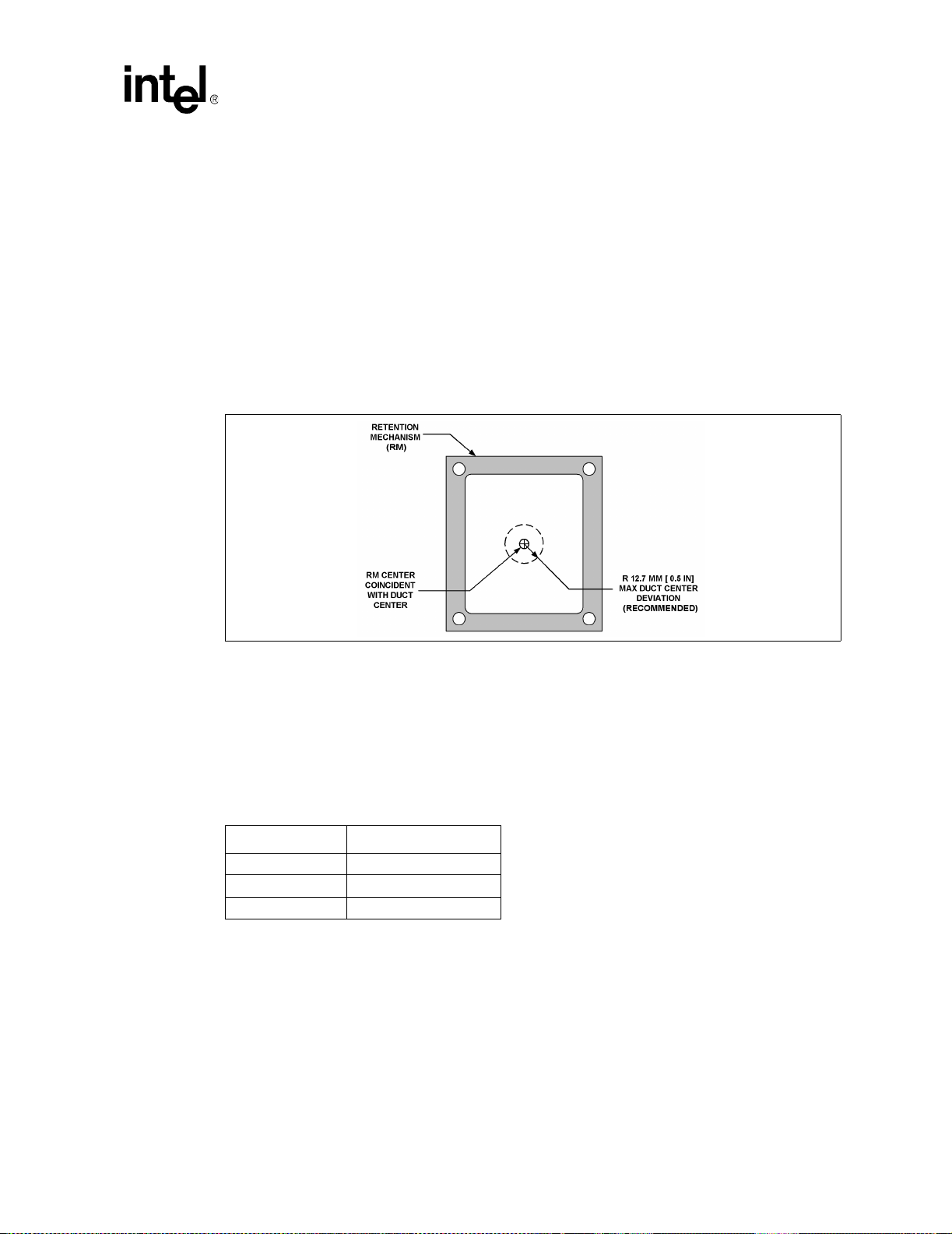
5.4 Processor Location Relative to Retention Mechanism
To ensure compatibility with chassis using a duct based on the reference Chassis Air Guide ducting
solution, the processor should be placed at a location corresponding to the center of the duct.
Information on duct position is available in the Desktop System Air Duct Design Suggestions. This
document is available on http://www.formfactors.org.
Board layouts should locate the center the processor heatsink retention mechanism within a
12.7 mm [0.5 inch] radius of the duct center location. Figure 5-22 illustrates the placement
guideline.
Figure 5-22. Processor Location Recommendation for Chassis Air Guide Relative to
Retention Mechanism
Front Side Bus (FSB)
5.5 Power Header for Active Cooling Solutions
The reference-design heatsink solution includes an integrated fan. The recommended connector for
the active cooling solution is a Walden/Molex 22-01-3037, AMP* 643815-3, or equivalent. The
integrated fan requires the system board to supply a minimum of 740 mA at 12 V for proper
operation. The fan connector pinout is described in Table 5- 22.
Table 5-22. Reference Solution Fan Power Header Pinout
Pin Number Signal
1 Ground
2 +12 V
3 No Connect
®
The Intel
connector for the active cooling solution is a Walden/Molex 22-23-2037, AMP* 640456-3, or
equivalent. The integrated fan requires the system board to supply a minimum of 740 mA at 12 V
for proper operation. The fan connector pinout is described in Table 5-23.
boxed processor heatsink solution includes an integrated fan. The recommended
Intel® 875P Chipset Platform Design Guide 81

Front Side Bus (FSB)
Table 5-23. Boxed Processor Fan Power Header Pinout
Pin Number Signal
1 Ground
2 +12 V
3 Sense
The fan heatsink outputs a SENSE signal which is an open-collector output that pulses at a rate of
two pulses per fan revolution. The system board requires a pull-up resistor to provide the
appropriate V
SENSE signal is not used, pin 3 should be tied to ground.
For more information on boxed processor requirements, refer to the processor datasheet.
level to match the fan speed monitor. Use of the SENSE signal is optional. If the
OH
5.6 Debug Port Guidelines
Refer to the latest revision of the processor Debug Port Design Guide for details on the
implementation of the debug port.
5.6.1 Debug Tools Specifications
5.6.1.1 Logic Analyzer Interface (LAI)
Intel is working with two logic analyzer vendors to provide logic analyzer interfaces (LAIs) for use
in debugging the Pentium 4 processor in the 478-pin package system. Tektronix and Agilent should
be contacted to get specific information about their logic analyzer interfaces. The following
information is general in nature. Specific information must be obtained from the logic analyzer
vendor.
Due to the complexity of Pentium 4 processor in the 478-pin package system, the LAI is critical in
providing the ability to probe and capture system bus signals. There are two sets of considerations
to keeping mind when designing a Pentium 4 processor in the 478-pin package system that can
make use of an LAI: mechanical and electrical.
5.6.1.2 Mechanical Considerations
The LAI is installed between the processor socket and the Pentium 4 processor in the 478-pin
package. The LAI pins plug into the socket, while the Pentium 4 processor in the 478-pin package
pins plug into a socket on the LAI. Cabling that is part of the LAI egresses the system to allow an
electrical connection between the Pentium 4 processor in the 478-pin package and a logic analyzer.
The maximum volume occupied by the LAI, known as the keep-out volume, as well as the gable
egress restrictions, should be obtained from the logic analyzer vendor. System designers must
make sure that the keep-out volume remains unobstructed inside the system. Note that it is possible
that the keep-out volume reserved for the LAI may include space normally occupied by the
Pentium 4 processor in the 478-pin package heatsink. If this is the case the logic analyzer vendor
will provide a cooling solution as part of the LAI.
5.6.1.3 Electrical Considerations
The LAI will also affect the electrical performance of the system bus; therefore, it is critical to
obtain the electrical load models from each of the logic analyzer vendors to be able to run system
level simulations to prove that their tool will work in the system. Contact the logic analyzer vendor
for electrical specifications and load models for the LAI solution they provide.
82 Intel
®
875P Chipset Platform Design Guide
DDR System Memory Guidelines
DDR System Memory Guidelines 6
The MCH memory interface consists of two DDR memory channels that can operate in either
single-channel or dual-channel modes. Each channel consists of 64 data bits.
This section covers routing guidelines for the DDR interface. Note that these guidelines apply to
both channel A and channel B. Each DDR interface has six signal groups: Clocks, Address/
Command, Data, Control, Receive Enable, and Miscellaneous. Table 6-1 summarizes the signal
groupings. The MCH contains two complete sets of these signals, one set per-channel. Refer to the
®
Intel
875P Chipset Datasheet for details on the signals listed in Table 6-1.
Refer to Chapter 15 for DDR power delivery considerations. The DDR guidelines are structured in
the following fashion:
• Section 6.5 contains guidelines necessary to implement a 2 DIMM per-channel solution. Using
these guidelines, the motherboard designer can choose to implement both 1 DIMM and 2
DIMM per-channel solutions.
• Section 6.6 details exceptions to the following guidelines for a 1 DIMM per-channel solution.
Table 6-1. MCH DDR Signal Groups
Section Group Signal Description
Section 6.5.2 Clocks
Section 6.5.4 Address/Command
Section 6.5.5 Data
Section 6.5.3 Control
N/A
(no external
connection)
NOTE: There are two sets of signals, one for Channel A and one for Channel B. The “x” in the signal name is
“A” for the channel A signal and “B” for the channel B signal. For example, the DDR differential clocks
for channel A are SCMDCLK_A[5:0].
Feedback
SCMDCLK_x[5:0]
SCMDCLK_x[5:0]#
SMAA_x[12:0]
SRAS_x#
SCAS_x#
SWE_x#
SBA_x[1:0]
SDQS_x[8:0]
SECC_x[7:0]
SDQ_x[63:0]
SCS_x[3:0]#
SCKE_x[3:0]
RCVENOUT#
RCVENIN#
DDR Differential Clocks
DDR Differential Inverted Clocks
Memory Address Bus
Row Address Select
Column Address Select
Write Enable
Bank Address (Bank Select)
Data Strobes
Check Bits for ECC Function
Data Bus
Chip Select
Clock Enable
Receive Enable Output
Receive Enable Input
Intel® 875P Chipset Platform Design Guide 83

DDR System Memory Guidelines
6.1 DDR Length Matching Strategy
6.1.1 Strategy Overview
Some insight can be gained if one considers the following prior to attempting to route the DDR
interface. There are two levels of length constraints placed on each signal group within the
interface. The absolute length constraints are provided in the constraint tables for each signal
group. These constraints define the length range over which the signals will meet signal integrity
rules. A subset of this solution space is then defined by a set of secondary length constraints which
are based on length matching to clock. The clock relative length matching formulas are not
concerned with signal integrity compliance, but purely based on clock relative timing margins.
These two sets of overlapping length constraints then define the final routing solution space.
It should also be noted that the absolute length constraints are based on motherboard routing
lengths, while the length matching formulas are based on pad-to-pin lengths. Therefore, care must
be taken when trying to reconcile the two sets of constraints with respect to each other. It is
recommended that an automated routing length spreadsheet be used to calculate motherboard
routing lengths as required to implement the length matching formulas. Only after package lengths
have been factored into the length matching formulas can motherboard lengths be compared
directly. In some cases motherboard length boundaries will be determined by the length matching
formulas, whereas in other cases the absolute motherboard length limits will come into play.
6.1.2 Defining the Target Clock Reference Length
Since all signal groups are directly or indirectly timing referenced back to clock, the clock is the
logical choice to serve as the master reference for all other signal groups, by way of length
matching formulas. It is recommended that following a preliminary test route establishing the
natural bounds on all signal groups, that target reference lengths be defined for each clock group
routed between the MCH and the DIMM connectors. Throughout this chapter, the target Clock
Reference length is defined as:
DIMM0 Clock: Target Reference Length = X0
DIMM1 Clock: Target Reference Length = X1
For optimal timing margins all clocks to a particular DIMM connector should be length tuned to
the target reference length for that DIMM. These reference lengths will then feed into the length
matching formulas to determine the secondary constraints on minimum and maximum length for
each signal group, as routed to the corresponding DIMM connector. Generally speaking the offset
in clock target length between DIMMs should be approximately equal to the routing length
between the DIMMs. This provides length matching consistency between DIMMs.
In some cases it is helpful to base the target clock lengths on the natural routing lengths of certain
critical path signals, as opposed to the natural lengths of the clocks themselves. In the case of the
MCH, the control group setup margin is a critical path. Therefore, it is recommended that the target
clock length be partially based on providing adequate setup margin as per the length matching
formula. This may require that the clocks be lengthened slightly from their natural length.
84 Intel
®
875P Chipset Platform Design Guide
DDR System Memory Guidelines
6.2 Length Matching and Length Formulas
The routing guidelines presented in the main body of this document define the recommended
routing topologies, trace width and spacing geometries, absolute minimum and maximum routed
lengths for each DDR signal group. This is recommended to meet signal integrity requirements. In
addition to the absolute length limits provided in the guideline tables for each signal group, more
restrictive length matching formulas are also provided that further restrict the minimum-tomaximum length range of each signal group with respect to the clock. These are within the overall
boundaries defined in the guideline tables, as required to guarantee adequate timing margins. These
secondary constraints are referred to as length matching constraints and the formulas used are
referred to as length matching formulas.
All signal groups except the clocks and feedback signals are length matched per slot to the
associated clocks, with the clocks themselves being length tuned to a fixed length range across
each DIMM slot. The amount of minimum-to-maximum length variance allowed for each group
around the clock reference length varies from signal group to signal group depending on the
amount of timing variance that can be tolerated. A simplified summary of the length matching
formulas for each signal group is provided in Tab le 6-2. As the table indicates, all signal groups are
somewhat biased in length to be shorter than the clock. This is done to optimize setup and hold
margins.
Table 6-2. Length Matching Formulas
Signal Group Minimum Length Maximum Length
Control to Clock Clock (max) – 2.0" Clock (min) – 0.5"
Command to Clock Clock (max) – 2.0" Clock (min) – 0.5"
Strobe to Clock Clock (max) – 2.0” Clock (min) + 1.0"
Data to Strobe Strobe – 25 mils Strobe +25 mils
NOTE: Note that all length matching formulas are based on MCH die-pad to DIMM pin total length.
Package length tables will be provided for all signals to facilitate this pad to pin matching. Note
that the clock length used for length matching may vary by DIMM slot, based on DIMM spacing.
Length formulas should be applied to each DIMM slot independently. The full geometry and
routing guidelines along with the exact length matching formulas and associated diagrams are
provided in the individual signal group guidelines sections to follow.
Note: For short clock lengths the command-to-clock maximum length rule can be slightly relaxed, due to
crisper clock edge rates and more setup margin at shorter lengths. See clock section for more
detailed information.
Intel® 875P Chipset Platform Design Guide 85
DDR System Memory Guidelines
6.3 Package Length Compensation
As mentioned briefly above, all length matching is MCH die-pad to DIMM pin. The reason for this
is to compensate for the package length variance across the signal group to minimize timing
variance. The MCH does not attempt to equalize package lengths internally as some previous MCH
components have, and therefore, requires a more tedious matching or tuning process. The
justification for this is based on the belief that length variance in the package based on ball position
will be at least partially tuned out when the pin escape is completed to the edge of the package.
Length matching in the package would then tend to create mismatch at the package edge.
Package length compensation should not be confused with length matching as discussed in the
previous section. Length matching, as discussed previously, refers to constraints on the minimum
and maximum length bounds of a signal group based on clock length, whereas package length
compensation refers to the process of adjusting out package length variance across a signal group.
There is, of course, some overlap in that both effect the target length of an individual signal. It is
recommend that a routing length spreadsheet be used to facilitate the package compensated
routing.
6.4 Stack-Up and Referencing Guidelines
Intel 875P chipset platform designs require ground referencing for all DDR signals. Based on a
typical four layer stack-up, the DDR channel requires the following stack-up to ground reference
all of the DDR signals from the MCH to the termination at the end of the channel. Note that the
DDR channel stack-up applies to the DDR channel only.
Table 6-3. DDR Channel Referencing Stack-Up
Motherboard Layer Description
Layer 1, Signal Top Signal/Power
Layer 2, Power Ground Cutouts
Layer 3, Ground Ground
Layer 4, Signal Bottom Signal/Power
A solid ground flood needs to be placed under the DDR channel on layer 2 from the MCH DDR
signal pins all the way beyond the DDR_TERM termination capacitors at the end of the channel to
provide an optimal return current path. Any split in the ground flood will provide a sub-optimal
return path.
86 Intel
®
875P Chipset Platform Design Guide
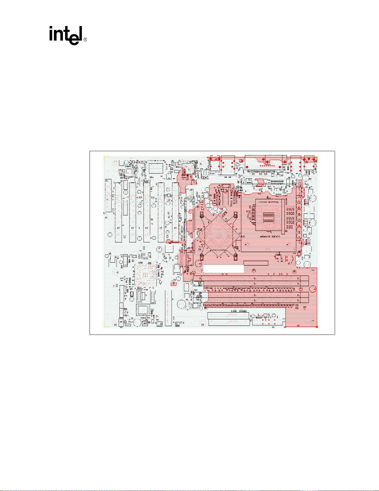
6.4.1 Ground Stitching
Ground floods must be well stitched to the ground plane on layer 3 to ensure the same potential
between the two planes. Any ground pin or ground via that is placed in the DDR routing area must
connect to both the ground flood and the ground plane.
It is also important to note that no power to the MCH is delivered on Layer 2; this is due to the
strict ground referencing requirements. As a result, this region on Layer 2 is a large ground flood.
Consequently, power must be delivered on Layers 1 and 4 (top and bottom); care must be taken to
allow for proper power delivery on these external layers. Refer to Chapter 15, “Power Distribution
Guidelines” for more information.
Figure 6-1. Example of Ground Flood on Layer 2
DDR System Memory Guidelines
Ground Flood
Intel® 875P Chipset Platform Design Guide 87
DDR System Memory Guidelines
6.5 DDR Design Topologies and Guidelines
The layout guidelines in this chapter were developed with the following design assumptions:
1. A standard 4-layer motherboard stack up (Signal, Power, Ground, Signal)
2. Two DDR channels, with one or two DIMMs each
3. All channel A DDR signals are routed on layer 1
4. All channel B DDR signals are routed on layer 4
Signals routed on Layer 4 (bottom) can use the last row of pins on the DIMM connector to
transition to Layer 1 (top) instead of using a via to get back to the top layer before reaching the
termination resistors.
Note: For 1 DIMM per-channel designs, refer to Section 6.6 for design considerations specific to a
1 DIMM per-channel implementation.
6.5.1 Target Impedances
The target impedances listed throughout Section 6.5 all refer to the area between MCH and first
DIMM.
Due to the congested routing in the DIMM connector and termination regions of the routing
channel, it is not possible to meet the target impedances in these regions. As a result, it is not
possible to maintain the target impedances once the signals reach the first DIMM connector. The
resulting guidelines for the DIMM connector regions do not meet the target impedance but have
been simulated and are believed to offer the best possible electrical characteristics given the
severely constrained routing area.
6.5.2 Clock Signal Group Routing Guidelines (SCMDCLK_x/SCMDCLK_x#)
The MCH clock signals include six differential clock pairs per-channel. The MCH generates and
drives these differential clock signals required by the DDR interface. Therefore, no external clock
driver is required for the DDR interface. Since the MCH only supports unbuffered DDR DIMMs,
\
Table 6-4. Clock Signal DIMM Mapping per DIMM
three differential clock pairs are routed to each DIMM connector.
Signal Relative To
SCMDCLK_x[2:0]
SCMDCLK_x[2:0]#
SCMDCLK_x[5:3]
SCMDCLK_x[5:3]#
DIMM 0
DIMM 1
DDR clocks can breakout of the MCH with reduced width (neckdown to 5 on 5) for a maximum
length of 500 mils; however, use of this reduced trace width should be minimized where possible.
Figure 6-2 shows an example of the clock neckdown in the MCH breakout.
88 Intel
®
875P Chipset Platform Design Guide
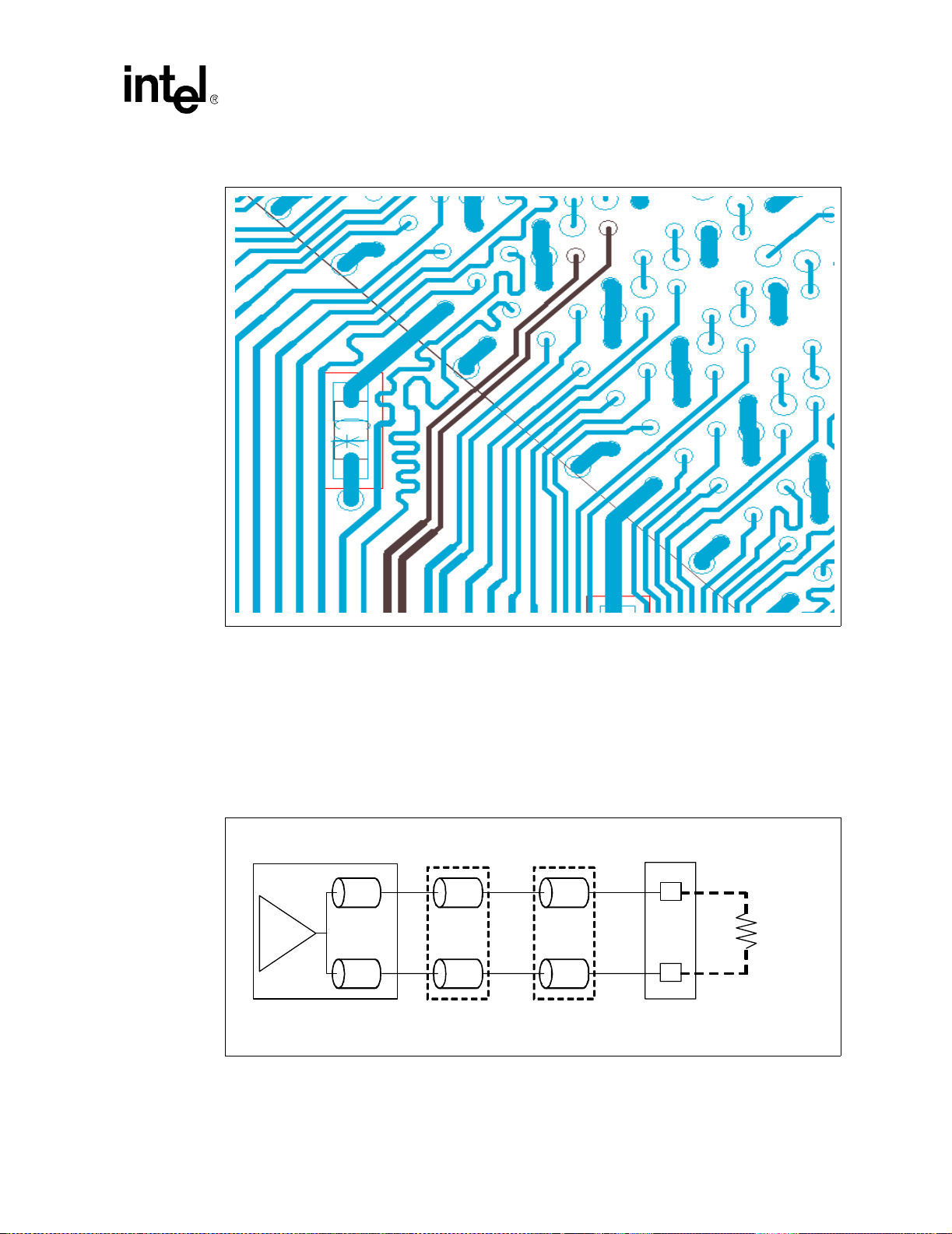
Figure 6-2. Example of DDR Clock Neckdown at MCH
DDR System Memory Guidelines
The clock pairs must be routed differentially from the MCH to their DIMM pins. They must
maintain correct spacing of 5 mils between themselves to remain differential. Additionally, the
clocks must maintain an isolation spacing of 20 mils away from other signals or from itself in a
serpentine.
There are no external termination resistors needed for the SCMDCLK_x/SCMDCLK_x# signals.
Figure 6-3 and Ta ble 6-5 depict the recommended topology and layout routing guidelines for the
DDR differential clocks.
Figure 6-3. DDR Differential Clock Routing Topology
MCH
P1
MCH
Pin
P1
L1
L1 L2
Differential
Pairs
DIMM
PADS
L2
R1*
* Located
on DIMM
Intel® 875P Chipset Platform Design Guide 89

DDR System Memory Guidelines
Table 6-5. Clock Signal Group Routing Guidelines
Parameter Definition
Signal Group SCMDCLK_x[5:0] and SCMDCLK_x[5:0]#
Topology Differential Pair Point-to-Point
Reference Plane Ground Referenced
Layer Assignment Layers 1 and 4 - Microstrip
Single-Ended Trace Impedance (Z
Differential Mode Impedance (Zdiff) 70 Ω ± 20%
Nominal Trace Width (see exceptions for
breakout region below)
Nominal Pair Spacing (edge to edge) 5 mils
Minimum Pair-to-Pair Spacing (see
exceptions for breakout region below)
Minimum Serpentine Spacing 20 mils
Minimum Spacing to Other DDR Signals
(see exceptions for breakout region below)
Minimum Isolation Spacing to Non-DDR
Signals
Maximum Via Count 2 (per side)
Package Length (P1) 750 mils ± 500 mils (see package length report)
Breakout Length (L1) Max = 500 mils
Total Motherboard Length Limits (L1 + L2)
Total Length Limits (P1 + L1 + L2) Max = 6.3 inches
Clock Target Lengths
SCLK to SCLK# Length Matching • Match total length to ± 10 mils
Clock-to-Clock Length Matching
(total length)
Breakout Exceptions
(reduced geometries for MCH breakout
region)
DIMM Field Exceptions
(reduced geometries for DIMM pin field
region)
) 42 Ω ± 15%
0
8 mils
20 mils
20 mils
20 mils
Min = 3.5 inches
Max = 6.0 inches
• Total length for DIMM0 group = X0 (See Section 6.1.2 for
target reference length X0 definition)
• Total length for DIMM1 group = X1 (See Section 6.1.2 for
target reference length X0 definition)
• Match all DIMM0 clocks to X0 ± 20 mils (See Section 6.1.2
for target reference length X0 definition)
• Match all DIMM1 clocks to X1 ± 20 mils (See Section 6.1.2
for target reference length X0 definition)
• Maximum clock length variance = 1.0 inch
• 5-mil trace with 5-mil pair space allowed
• 5-mil pair to pair spacing allowed
• 10-mil spacing to other DDR signals allowed
• Maximum breakout length is 0.5 inch
• 6-mil trace with 5-mil pair space allowed
• Maximum reduced trace width length is 1.5 inches
• 10-mil spacing to other DDR signals allowed
• Maximum reduced spacing length is 1.0 inch
NOTES:
1. Overall target length should be established based on test route results and a cursory review of length
matching formulas. In particular, the target length should be set to a minimum of the longest control signal
length plus 1.5 inches, in order to optimize that path. Once the target length is established, all clocks to that
DIMM should be length tuned to the target length as defined. The resulting motherboard segment lengths of
each clock must fall within the ranges specified.
90 Intel
®
875P Chipset Platform Design Guide
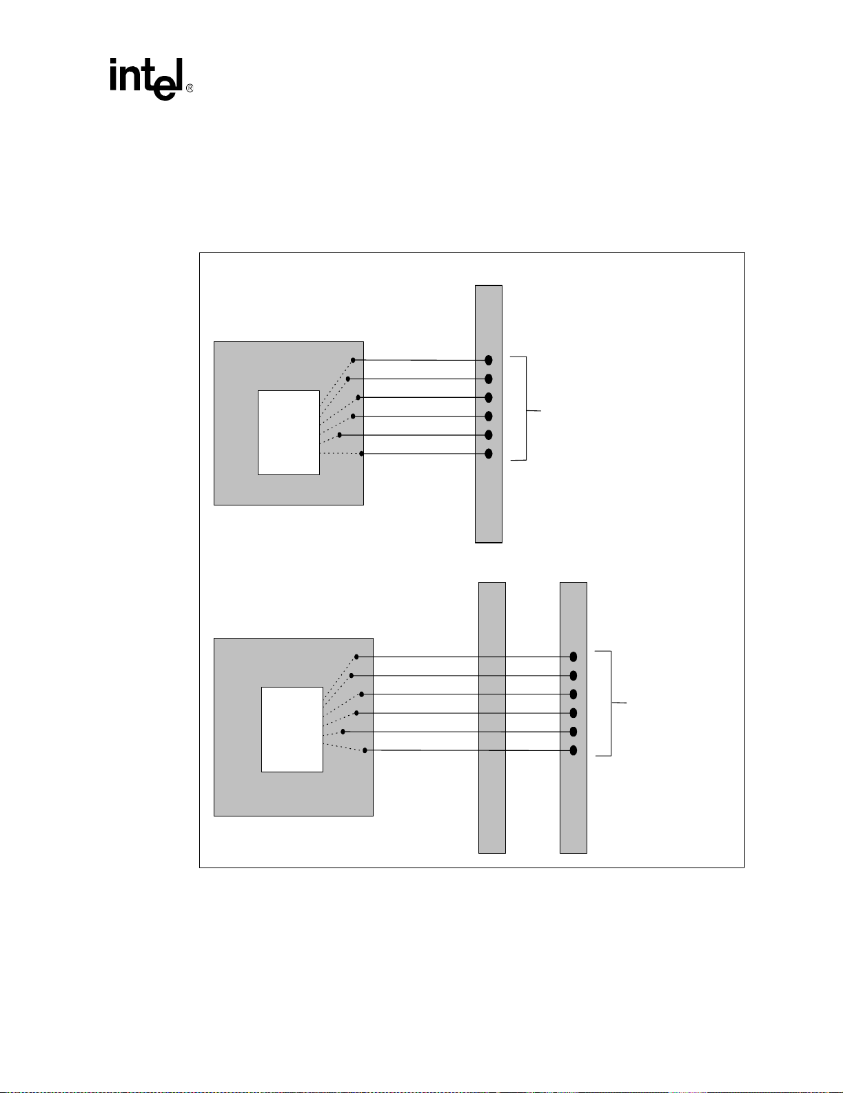
2. The difference in target length between DIMM0 clocks and DIMM1 clocks should be approximately
equivalent to the routing distance between DIMMs; this facilitates length matching on bussed signals. The
maximum length variance across all clocks should not exceed 1.0 inch, as defined above.
3. Exceptions to the trace width and spacing geometries are allowed in the breakout region to fanout the
interconnect pattern. Reduced spacing should be avoided as much as possible. Reduced trace width and
spacing is also allowed in DIMM pin field region. Once reduced, the trace should stay reduced to final
connection.
Figure 6-4. Clock-to-Clock Length Matching Requirements
DIMM 0
Clock Reference Length X0 = _______
DDR System Memory Guidelines
MCH Package
MCH
Die
Clock Reference Length X1 = _______
MCH Package
MCH
Die
CMDCLK_x0
CMDCLK_x0#
CMDCLK_x1
CMDCLK_x1#
CMDCLK_x2
CMDCLK_x2#
CMDCLK_x3
CMDCLK_x3#
CMDCLK_x4
CMDCLK_x4#
CMDCLK_x5
CMDCLK_x5#
DIMM 0
CMDCLK_x0 = X
CMDCLK_x0# = X
CMDCLK_x1= X
CMDCLK_x1# = X
CMDCLK_x2 = X
CMDCLK_x2# = X
DIMM 1
CMDCLK_x3 = X1
CMDCLK_x3# = X1
CMDCLK_x4 = X1
CMDCLK_x4# = X1
CMDCLK_x5 = X1
CMDCLK_x5# = X1
NOTE: All lengths are measured from MCH die pad to DIMM connector pad.
Intel® 875P Chipset Platform Design Guide 91

DDR System Memory Guidelines
6.5.3 Control Signal Group Routing Guidelines (SCKE_x[3:0]#, SCS_x[3:0]#)
The MCH control signals that include the enable (SCKE_x) and chip select (SCS_x#) are sourceclocked signals. One SCKE_x and SCS_x# are needed per row. SCKE_x and SCS_x# are tuned to
SCMDCLK_x.
Table 6-6. Control Signal-to-DIMM Mapping
Control Signal Mapping
(per Channel)
SCKE_x[1:0] DIMM 0
SCS_x[1:0]# DIMM 0
SCKE_x[3:2] DIMM 1
SCS_x[3:2}# DIMM 1
Relative To
Table 6-7, Figure 6-5, and Figure 6-6 depict the recommended topology and layout guidelines for
.
the DDR control signals.
Figure 6-5. Control Signal Group Routing Topology
MCH
MCH
Pin
P1
Breakout
Table 6-7. Control Signal Group Routing Guidelines
Parameter Definition
Signal Group SCKE_x[3:0], SCS_x[3:0]#
Topology Point-to-Point with Parallel Termination
Reference Plane Ground Referenced
Layer Assignment Layers 1 and 4 - Microstrip
Characteristic Trace Impedance (Z
Nominal Trace Width 5 mils
Minimum Trace-to-Trace Spacing
(see breakout and DIMM field exception below)
Minimum Isolation Spacing to Non-DDR
Signals
Package Length (P1) 750 mils ± 500 mils (see package length report)
Breakout Length (L1) Max = 550 mils
Total Length (L1+ L2), MCH to First DIMM Pad
) 60 Ω ± 15%
0
L1
12 mils
20 mils
Min = 1.5 inches
Max = 5.0 inches
L2
Vtt
Rt
L3
DIMM0,1 PAD
92 Intel
®
875P Chipset Platform Design Guide

Table 6-7. Control Signal Group Routing Guidelines (Continued)
Parameter Definition
Trace Length (L3), Last DIMM Pad to Parallel
Termination Resistor Pad
Parallel Termination Resistor (Rt) 47 Ω ± 5%
Maximum Recommended Motherboard Via
Count
CTRL to SCMDCLK Length Matching
(Total length including package)
Breakout Exceptions
(Reduced geometries for MCH breakout
region)
DIMM Field Exceptions
(Reduced geometries for DIMM pin field
region)
NOTES:
1. The actual motherboard routed length to each DIMM must fall within the range defined by the clock length
matching formulas, based on the clock target length. The length limits defined in this table represent absolute
limits for acceptable signal integrity.
2. Power distribution vias from Rt to VTT are not included in via count.
3. The reduced spacing exception in the DIMM field refers to total reduced spacing length. This region can
include either DIMM field as well as the routing segment to Rt.
Max = 1.2 inches
2
(CLKmax – 2.0 inches) < CTRL < (CLKmin – 0.5 inch)
See length matching section for details
5-mil spacing to other DDR signals allowed
Maximum breakout length is 0.5 inch
5-mil spacing to other DDR signals allowed
Maximum reduced spacing length is 1.5 inches total.
DDR System Memory Guidelines
Intel® 875P Chipset Platform Design Guide 93

DDR System Memory Guidelines
Figure 6-6. Control Signal-to-Clock Length Matching Requirements
DIMM 0
MCH Package
MCH
DIE
SCS_x[1:0]#, SCKE_x[1:0]
CMDCLK_x[2: 0]
CMDCLK_x[2: 0]#
CTRL Length = Y0
(X0max – 2.0") ≤ Y0 ≤ (X0m in – 0.5")
Clock Refer ence Length = f(X)
DIMM 0 DIMM 1
MCH Package
MCH
DIE
SCS_x[3:2 ]#, SCKE_x[3: 2]
CMDCLK_x[5: 3]
CMDCLK_x[5: 3]#
NOTE: All lengths are measured from MCH die pad to DIMM connector pad.
CTRL Length = Y1
(X1max – 2.0") ≤ Y1 ≤ (X1m in – 0.5" )
Clock Referenc e Length = X1
94 Intel
®
875P Chipset Platform Design Guide

DDR System Memory Guidelines
6.5.4 Address/Command Signal Group Routing Guidelines
(SMAA_x[12:0], SBA_x[1:0], SRAS_x#,
SCAS_x#, SWE_x#)
The MCH address/command signals are source-clocked signals that include memory address
signals SMAA_x[12:0], SBA_x[1:0], SRAS_x#, SCAS_x#, SWE_x#. The address/command
signals are tuned to SCMDCLK_x.
Figure 6-7, Figure 6-8, and Tab le 6- 8 depict the recommended topology and routing guidelines for
the DDR address/command signals.
Figure 6-7. DDR Address/Command Routing Topology
MCH
MCH
Die
P1
L1
L2
L3
Breakout
Table 6-8. Address/Command Signal Group Routing Guidelines
Parameter Definition
Signal Group
Topology Daisy Chain with Parallel Termination
Reference Plane Ground Referenced
Layer Assignment Layers 1 and 4 - Microstrip
Characteristic Trace Impedance (Z
Nominal trace width
Minimum Trace-to-Trace Spacing
(see breakout and DIMM field exceptions below)
Minimum isolation spacing to non-DDR Signals 20 mils
Package Length (P1) 750 mils ± 500 mils (see package length report)
Breakout Length (L1) Max = 500 mils
Total Length (L1 + L2), MCH to First DIMM Pad Min = 1.5 inches
Trace Length (L3), First DIMM Pad to Last DIMM
Pad
Total Motherboard Length (L1+ L2 + L3), MCH Ball
to Last DIMM Pad
Total Length (P1 + L1+ L2 + L3), MCH Die to Last
DIMM Pad
Trace Length (L4), Last DIMM Pad to Parallel
Termination Resistor Pad
Parallel Termination Resistor (Rt) 47 Ω ± 5%
)
0
SMAA_x[12:0], SBA_x[1:0], SRAS_x#, SCAS_x#,
SWE_x#
L2 segment: 50 Ω ± 15%
L1, L3, and L4 segments: 60 Ω ± 15%
L2 segment: 7 mils
L1, L3, and L4 segments: 5 mils
12 mils
Min = 0.2 inch
Max = 0.6 inch
Max = 5.0 inches
Max = 5.3 inches
Max = 1.0 inch
Vtt
Rt
L4
DIMM1 PADDIMM0 PAD
Intel® 875P Chipset Platform Design Guide 95
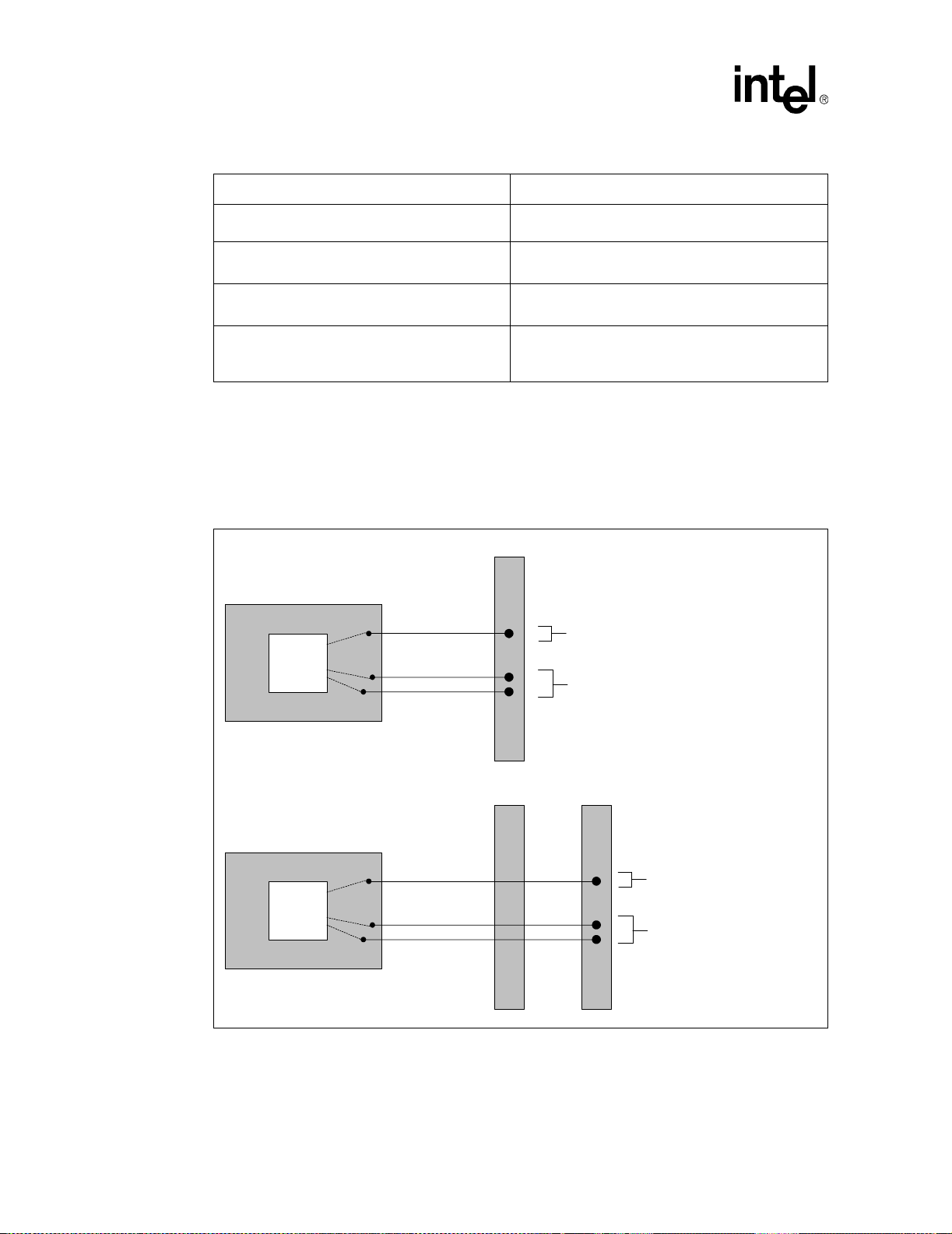
DDR System Memory Guidelines
Table 6-8. Address/Command Signal Group Routing Guidelines (Continued)
Parameter Definition
Maximum Recommended Motherboard Via Count
Per Signal
CMD to SCMDCLK Length Matching
(total length including package)
Breakout Exceptions
(reduced geometries for MCH breakout region)
DIMM Field Exceptions
(reduced geometries for DIMM pin field region)
2
• (CLKmax – 2.0”) < CMD < (CLKmin – 0.5”)
• See length matching section for details
• 5-mil spacing to other DDR signals allowed
• Maximum breakout length is 0.5 inch
• 5-mil spacing to other DDR signals allowed
• Maximum reduced spacing length is 1.5 inches
total
NOTES:
1. The actual motherboard routing length to each DIMM must fall within the range defined by the clock length
matching formulas, based on the clock target length. The limits defined in this table represent absolute limits
for acceptable signal integrity.
2. The routing distance between DIMMs can be as little as 0.2 inch or as much as 0.6 inch. However, in a given
design the amount of variance across a signal group should be minimized to facilitate length matching.
3. Power distribution vias from Rt to VTT are not included in via count.
Figure 6-8. Address/Command-to-Clock Length Matching Requirements
MCH Package
MCH Package
MCH
DIE
MCH
DIE
SMAA_x[12:0]#,
SBA_x[1:0], SRAS_x#,
SCAS_x#, SWE_x #
CMDCLK_x[2:0]
CMDCLK_x[2:0] #
SMAA_x[12:0]#,
SBA_x[1:0], SRAS_x#,
SCAS_x#, SWE_x #
CMDCLK_x[5:3]
CMDCLK_x[5:3] #
DIMM 0
CMD Length = Y0
(X0max – 2.0") ≤ Y0 ≤ (X0min – 0.5")
Clock Reference Length = f(X)
DIMM 0 DIMM 1
CMD Length = Y1
(X1max – 2.0") ≤ Y1 ≤ (X1min – 0.5")
Clock Reference Length = X1
NOTE: All lengths are measured from MCH die pad to DIMM connector pad.
96 Intel
®
875P Chipset Platform Design Guide
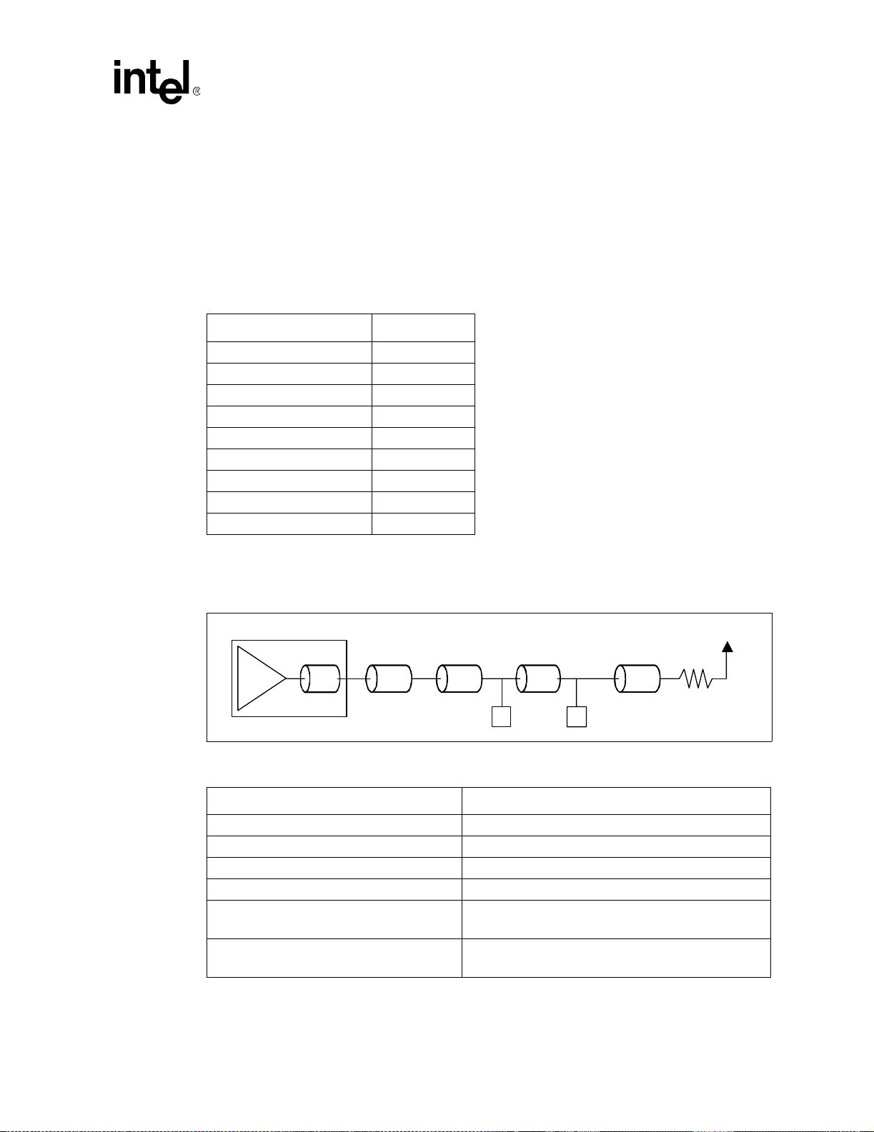
6.5.5 Data Signal Group Routing Guidelines (SDQ_x[63:0], SDQS_x[8:0], SECC_x[7:0])
The MCH DDR data signals are source synchronous signals, each channel includes the 64-bit wide
data bus, eight data strobe signals, and eight ECC signals. There is an associated data strobe
(SDQS
_x) for each data group. Table 6-9 summarizes the SDQ_x and SECC_x to SDQS_x
mapping. SDQ
signals are tuned to SCMDCLK
Table 6-9. SDQ and SECC to SDQS Mapping
SDQ_x[8:0] SDQS0
SDQ_x[15:8] SDQS1
SDQ_x[23:16] SDQS2
SDQ_x[31:24] SDQS3
SDQ_x[39:32] SDQS4
SDQ_x[47:40] SDQS5
SDQ_x[55:48] SDQS6
SDQ_x[63:56] SDQS7
SECC_x[7:0] SDQS8
_x and SECC_x signals are tuned to their associated SDQS_x signal, and SDQS_x
_x lengths.
SDQ/SDM SDQS
DDR System Memory Guidelines
Table 6- 10, Figure 6-9, and Figure 6-10 depict the recommended topology and layout routing
guidelines for the DDR data signals.
Figure 6-9. Data Signal Routing Topology
MCH
MCH
Die
P1
L1
L2
Breakout
Table 6-10. Data Signal Group Routing Guidelines
Parameter Definition
Signal Group SDQ[63:0], SECC[7:0], SDQS[8:0]
Topology Daisy Chain with Parallel Termination
Reference Plane Ground Referenced
Layer Assignment Layers 1 and 4 - Microstrip
Characteristic Trace Impedance (Z
Nominal Trace Width
)
0
Vtt
Rt
L3
L4
DIMM1 PADDIMM0 PAD
L2 Segment = 50 Ω ± 15% (40 Ω for length > 5.7 inches)
L1, L3 and L4 Segments = 60 Ω ± 15%
L2 Segment = 7 mils (11 mils for length > 5.7 inches)
L1, L3 and L4 Segments = 5 mils
Intel® 875P Chipset Platform Design Guide 97
DDR System Memory Guidelines
Table 6-10. Data Signal Group Routing Guidelines (Continued)
Parameter Definition
Minimum Trace-to-Trace Spacing
(see breakout and DIMM field exception below)
Minimum iSolation Spacing to Non-DDR Signals 20 mils
Package Length (P1) 750 mils ± 500 mils (see package length report)
Breakout Length (L1) Max = 550 mils
Total length (L1 + L2), MCH Ball to First DIMM
Pad
Trace Length (L3), First DIMM Pad to Last
DIMM Pad
Total Length (L1 + L2 + L3), MCH Ball to Last
DIMM Pad
Total Length (P1 + L1+ L2 + L3), MCH Die to
Last DIMM Pad
Trace length (L4), Last DIMM Pad to
Termination Resistor Pad
Parallel Termination Resistor (Rt) 56 Ω ± 5%
Maximum Recommended Motherboard Via
Count Per Signal
SDQS to SCMDCLK Length Matching
(total length including package)
SDQ/SECC to SDQS Length Matching
(total length including package)
Breakout Exceptions
(reduced geometries for MCH breakout region)
DIMM Field Exceptions
(reduced geometries for DIMM pin field region)
SDQ signals: 12 mils (15 mils for length > 5.7 inches)
SDQS signals: 15 mils (17 mils for length > 5.0 inches)
Min = 1.5 inches
Min = 0.2 inch
Max = 0.6 inch
Max = 6.5 inches
Max = 6.9 inches
Max = 1.0 inch
2
• (CLKmax - 2.0") < SDQS < (CLKmin + 1.0 inch)
• See length matching section for details
• Match SDQ/SECC to SDQS, to ± 25 mils, per byte
lane
• See length matching sections
• 5-mil trace allowed
• 5-mil spacing to other DDR signals allowed
• Maximum breakout length is 0.5 inch
• 5-mil trace allowed
• 5-mil spacing to other DDR signals is allowed
(DQ only)
• 10 mil spacing to other DDR signals is allowed
(DQS only)
• Maximum reduced spacing length is 2.5 inches total
NOTES:
1. The actual MB routing length to each DIMM must fall within the range defined by the clock length matching
formulas, based on the clock target length. The limits defined in this table represent absolute limits for
acceptable signal integrity.
2. The width and spacing rules for DQ and DQS routing are length dependent as shown in the table. Note that
the length cutoff of 5.7 inches refers to the total combined MB and package length (P1 + L1 + L2 + L3).
3. When implementing the wider 11-mil trace width rule on long byte lanes the wider trace width should be
implemented on all DQ and DQS signals within a byte lane or none. Also note that if required the higher trace
width should be achieved incrementally by transitioning to 7 mils for up to 1.0 inch additional length following
the breakout region before transitioning to 11 mils. If required an addition region of 9 mils could be used for
up to 1.0 inch additional length following the 7-mil region. It is not required that these stepping lengths be
matched exactly across each trace in a byte lane. Also note that normal L2 spacing rules apply for the
transition region.
4. The routing distance between DIMMs (L3) can be as little as 0.2 inch or as much as 0.6 inch, however, in a
given design the amount of variance across a signal group or bus should be minimized in order to facilitate
and optimize length matching.
98 Intel
®
875P Chipset Platform Design Guide
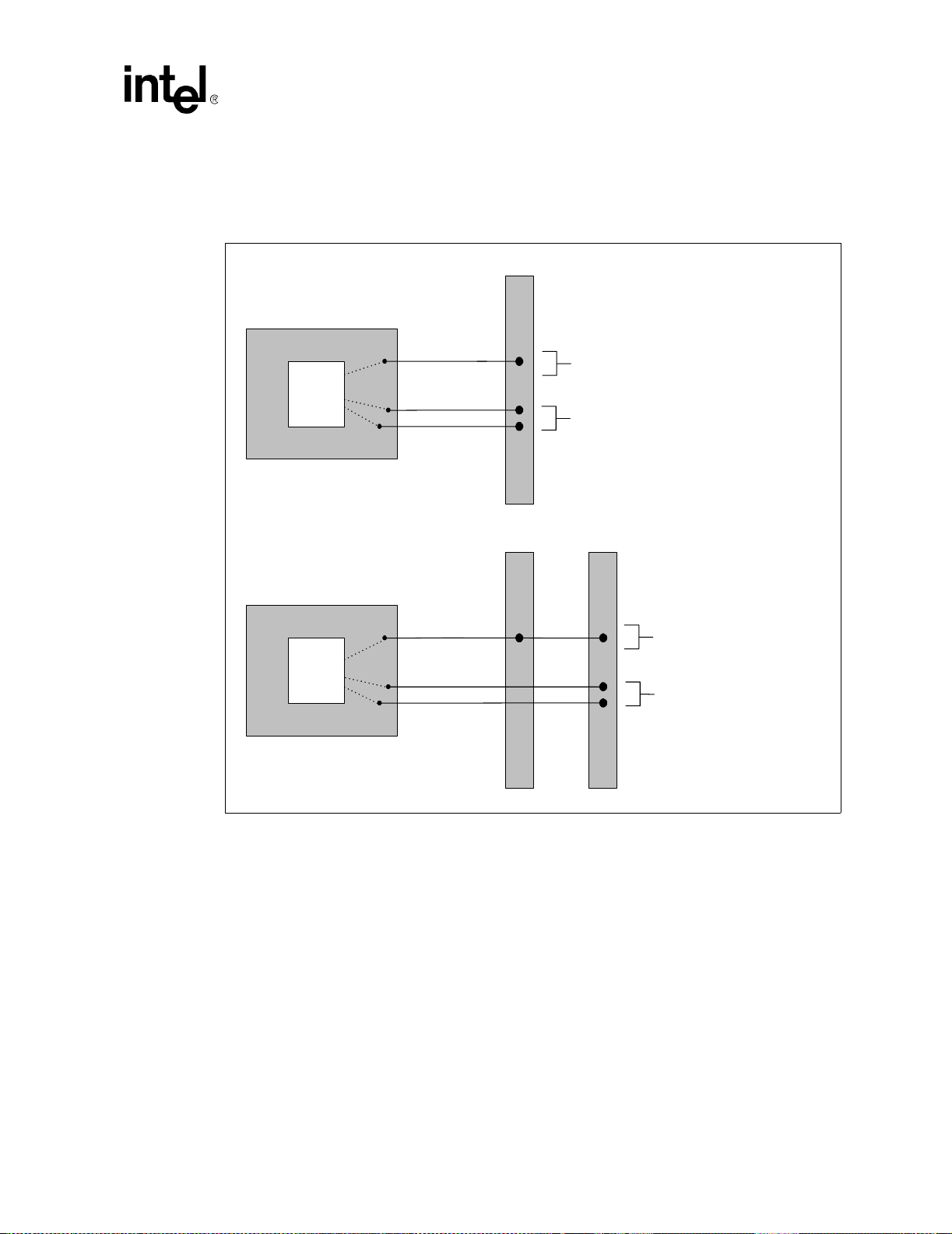
5. The DIMM pin field exception region is defined to include the DIMM pin field and termination region for each
channel, but also includes any reduced spacing region in channel B routing required to route through the
channel A pin field region.
6. Power distribution vias from Rt to VTT are not included in via count.
Figure 6-10. SDQS-to-Clock Length Matching Requirements
DIMM 0
DDR System Memory Guidelines
MCH Package
MCH
Die
MCH Package
MCH
Die
SDQS_x[8:0]
CMDCLK_x[2:0]
CMDCLK_x[2:0]#
DQS_x[8:0]
CMDCLK_x[5:3]
CMDCLK_x[5:3]#
SDQS Length = Y0, where
(X0max – 2.0") ≤ Y0 ≤ (X0min + 1.0")
Clock Reference Length = X
DIMM 0 DIMM 1
DQS_x Length >= X - 2.85"
(X1max – 2.0") ≤ Y1 ≤ (X1min + 1.0")
Clock Reference Length = X1
NOTE: All lengths are measured from MCH die pad to DIMM connector pad.
Intel® 875P Chipset Platform Design Guide 99
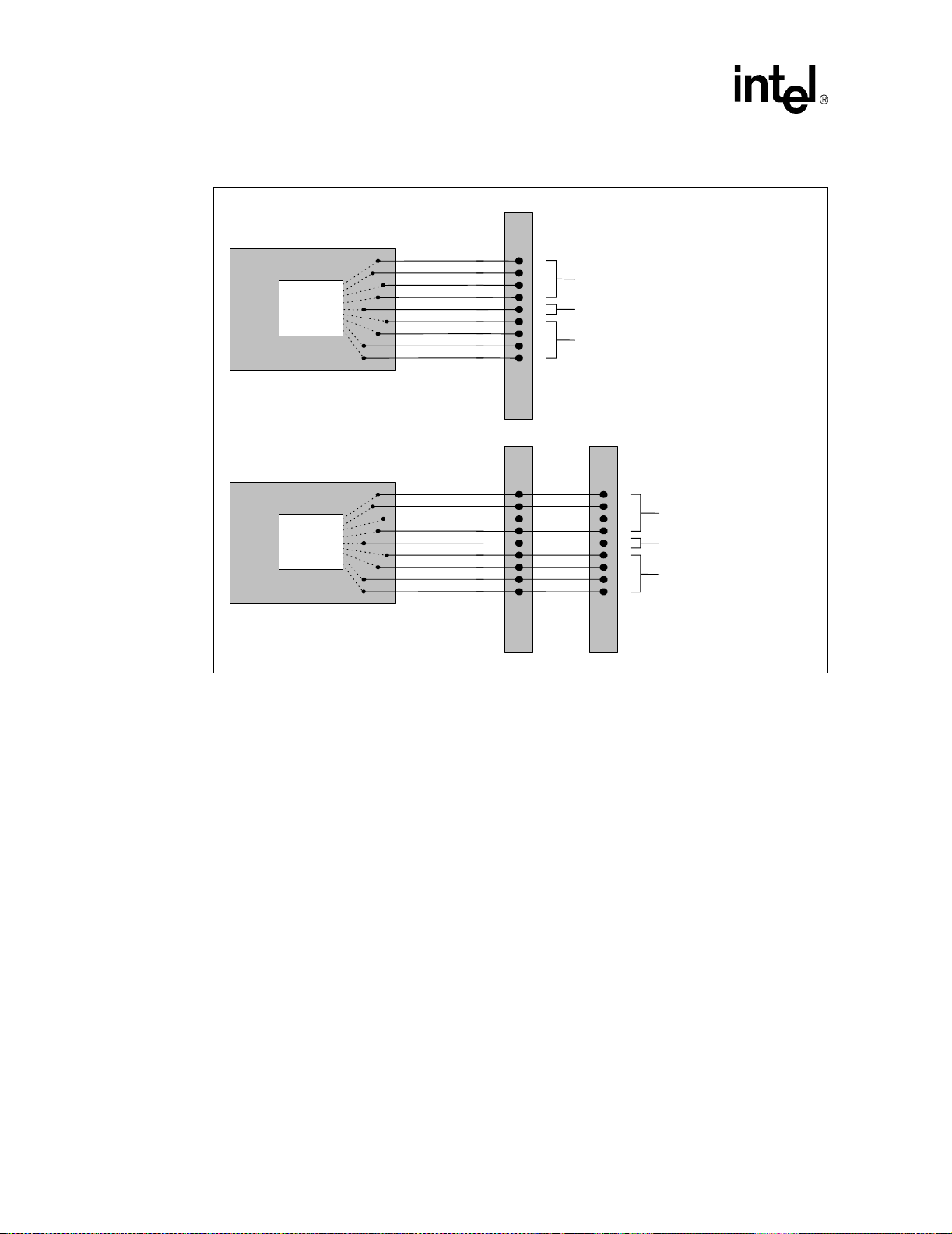
DDR System Memory Guidelines
Figure 6-11. SDQ/SECC-to-SDQS Length Matching Requirements
DIMM 0
MCH
Package
MCH
Die
Note: Only one byte lane i s shown for reference.
Each byte lane is mat ched independent ly.
MCH
Package
MCH
Die
SDQ_x0
SDQ_x1
SDQ_x2
SDQ_x3
SDQS_x0
SDQ_x4
SDQ_x5
SDQ_x6
SDQ_x7
SDQ_x0
SDQ_x1
SDQ_x2
SDQ_x3
SDQS_x0
SDQ_x4
SDQ_x5
SDQ_x6
SDQ_x7
SDQ Length (Y) = (X ± 25 mils)
SDQS Length = X
SDQ Length (Y) = (X ± 25 mils)
DIMM 0 DIMM 1
NOTE: All lengths are measured from MCH die pad to DIMM connector pad.
SDQ Length (Y) = (X ± 25 mils)
SDQS Length = X
SDQ Length (Y) = (X ± 25 mils)
100 Intel
®
875P Chipset Platform Design Guide
 Loading...