


h
R
®
Intel
Xeon™ Processor and
Intel® 860 Chipset Platform
Design Guide
Document Number: 298252-004

R
Information in this document is provided in connection with Intel® products. No license, express or implied, by estoppel or otherwise, to any intellectual
property rights is granted by this document. Except as provided in Intel’s Terms and Conditions of Sale for such products, Intel assumes no liability
whatsoever, and Intel disclaims any express or implied warranty, relating to sale and/or use of Intel products including liability or warranties relating to
fitness for a particular purpose, merchantability, or infringement of any patent, copyright or other intellectual property right. Intel products are not
intended for use in medical, life saving, or life sustaining applications.
Intel may make changes to specifications and product descriptions at any time, without notice.
Designers must not rely on the absence or characteristics of any features or instructions marked “reserved" or "undefined." Intel reserves these for
future definition and shall have no responsibility whatsoever for conflicts or incompatibilities arising from future changes to them.
®
The Intel
from published specifications. Current characterized errata are available on request.
Contact your local Intel sales office or your distributor to obtain the latest specifications and before placing your product order.
I
Implementations of the I
Corporation.
Alert on LAN is a result of the Intel-IBM Advanced Manageability Alliance and a trademark of IBM
Copies of documents which have an ordering number and are referenced in this document, or other Intel literature, may be obtained by calling
1-800-548-4725 or by visiting Intel’s website at http://www.intel.com .
Intel, Intel logo, Pentium, Intel NetBurst, and Intel Xeon are trademarks or registered trademarks of Intel Corporation or its subsidiaries in the United
States and other countries.
*Other names and brands may be claimed as the property of others.
Copyright
Xeon™ processor and Intel
2
C is a two-wire communications bus/protocol developed by Philips. SMBus is a subset of the I2C bus/protocol and was developed by Intel.
©
Intel Corporation 2001-2002
2
C bus/protocol may require licenses from various entities, including Philips Electronics N.V. and North American Philips
®
860 chipset may contain design defects or errors known as errata which may cause the product to deviate
®
2 Intel
Xeon™ Processor and Intel® 860 Chipset Platform Design Guide

R
Contents
1 Introduction ........................................................................................................................19
1.1 Related Documentation ........................................................................................20
1.2 Conventions and Terminology ..............................................................................22
1.3 System Overview ..................................................................................................25
1.3.1 Processor Overview ..............................................................................25
1.3.2 Intel® 860 Chipset..................................................................................26
1.3.2.1 Memory Controller Hub (MCH) ............................................26
1.3.2.2 I/O Controller Hub 2 (Intel® ICH2)........................................27
1.3.2.3 Memory Repeater Hub for Direct RDRAM* Device
1.3.2.4 PCI 64-Bit Hub (Intel® P64H) ...............................................28
1.3.3 Bandwidth Summary .............................................................................28
1.3.4 System Configurations ..........................................................................29
1.4 Platform Initiatives................................................................................................. 30
1.4.1 Memory Expansion Card (MEC) and Connector (MECC).....................30
1.4.2 Intel® 860 Chipset MCH.........................................................................30
1.4.2.1 Direct RDRAM* Device Interface .........................................30
1.4.2.2 Accelerated Graphics Port (AGP) ........................................30
1.4.3 Intel® ICH2.............................................................................................31
1.4.3.1 Integrated LAN Controller ....................................................31
1.4.3.2 Audio Codec ’97 (AC’97) 6-Channel Support ......................32
1.4.3.3 Low Pin Count (LPC) Interface ............................................33
1.4.3.4 Ultra ATA .............................................................................33
1.4.3.5 Universal Serial Bus (USB) ..................................................34
1.4.4 Manageability ........................................................................................34
1.5 Platform Compliance ............................................................................................35
1.5.1 PC 99/2001............................................................................................35
®
MRH-R) .....................................................................28
(Intel
2 Component Layout ............................................................................................................37
2.1 Intel® Xeon™ Processor Component Quadrant Layout........................................37
2.2 Intel® 860 Chipset Component Quadrant Layout ..................................................40
3 Platform Stack-Up and Placement Overview ....................................................................43
3.1 Platform Component Placement...........................................................................43
3.2 Two-Way System Stack-Up ..................................................................................45
3.2.1 Design Recommendations ....................................................................45
3.2.1.1 Stack-Up Option A ...............................................................45
3.2.1.2 Stack-Up Option B ...............................................................46
3.2.2 Design Considerations ..........................................................................46
3.2.2.1 Stack-Up Example A ............................................................47
3.2.2.2 Stack-Up Example B ............................................................48
4 Platform Clock Routing Guidelines....................................................................................51
4.1 Routing Guidelines for Host Clocks ......................................................................52
4.2 Routing Guidelines for Direct Rambus* Clock Generators (DRCG Devices) .......57
4.2.1 CKx_SKS to DRCG: Reference Clocks ................................................57
®
Xeon™ Processor and Intel® 860 Chipset Platform Design Guide 3
Intel

4.2.2
MCH to DRCG* Device: Phase Aligning Clocks ...................................58
4.2.3 DRCG* Device Signals to Rambus* Channels
(300 MHz/400 MHz Clocks) ..................................................................58
4.2.3.1 Trace Length Recommendations.........................................59
4.2.3.2 Topology Considerations .....................................................61
4.2.3.3 Clock Termination ................................................................61
4.2.4 DRCG* Device Impedance Matching Circuit.........................................62
4.2.5 DRCG* Device Layout Example............................................................64
4.3 Routing Guidelines for 66 MHz and 33 MHz Clocks.............................................65
4.3.1 66 MHz/33 MHz Clock Relationships ....................................................65
4.3.2 66 MHz Clock Routing Length Guidelines.............................................65
4.3.3 33 MHz Clock Routing Length Guidelines.............................................67
4.3.4 Intel® P64H PCI Clock Routing Guidelines............................................68
4.3.4.1 Intel® P64H PCI 33 MHz Clock Routing Guidelines.............68
4.3.4.2 Intel® P64H PCI 66 MHz Clock Routing Guidelines.............69
5 System Bus Routing ..........................................................................................................71
5.1 Return Path...........................................................................................................72
5.2 Serpentine Routing ...............................................................................................73
5.3 System Bus Decoupling Requirements ................................................................73
5.3.1 Processor I/O Decoupling Requirements..............................................74
5.4 Dual Processor Configuration ...............................................................................75
5.4.1 Routing Guidelines for Source Synchronous Signals............................77
5.4.1.1 4X Group (DSTBN[3:0]#, DSTBP[3:0]#, D[63:0]#,
DBI[3:0]#):............................................................................79
5.4.1.2 2X Group (ADSTB[1:0]#, A[35:3]#, REQ[4:0]#) ...................81
5.4.1.3 Common Clock ....................................................................81
5.4.1.4 Wired-OR Signals (BINIT#, BNR#, HIT#, HITM#,
MCERR#).............................................................................81
5.4.2 Routing Guidelines for Asynchronous GTL+ and Other System Bus
Signals...................................................................................................83
5.4.2.1 Topology 1: Asynchronous GTL+ Signals Driven by the
Processor.............................................................................84
5.4.2.2 Topology 2: Asynchronous GTL+ Signals Driven by the
Chipset.................................................................................87
5.4.2.3 Topology 3: VID[4:0] ............................................................87
5.4.2.4 Topology 4: SMBus Signals .................................................88
5.4.2.5 Topology 5: BR[3:0]# Signals...............................................90
5.4.2.6 Topology 6: COMP[1:0] Signals...........................................90
5.4.2.7 Topology 7: ODTEN Signal.................................................. 91
5.4.2.8 Topology 8: TESTHI[6:0] Signals.........................................91
5.4.2.9 Topology 9: SKTOCC# Signal .............................................92
5.5 MCH System Bus Interface...................................................................................93
5.5.1 MCH System Bus I/O Decoupling Recommendations ..........................94
R
6 Memory Interface Routing .................................................................................................97
6.1 Rambus* Channel Overview.................................................................................97
6.2 Memory Design with MEC/MECC (Inner Layer Routing)......................................98
®
4 Intel
Xeon™ Processor and Intel® 860 Chipset Platform Design Guide

R
6.3
Rambus* Channel Routing Guidelines .................................................................99
6.3.1 Rambus* Signaling Level (RSL) Signals ............................................. 100
6.3.2 Rambus Signaling Level (RSL) Channel Compensation.....................102
6.3.2.1 Package Trace Compensation
(RSL and Clocking Signals) ...............................................102
6.3.2.2 Via Compensation.............................................................. 104
6.3.2.3 Differential Clock Compensation .......................................105
6.3.2.4 Signal Layer Alteration for RIMM* Connector Pin
Compensation....................................................................105
6.3.2.5 RIMM* Connector Impedance Compensation ...................106
6.3.3 RSL Signal Termination ......................................................................110
6.3.4 Direct RDRAM* Device Reference Voltage.........................................111
6.3.5 High Speed CMOS Routing.................................................................112
6.3.6 SIO Routing.........................................................................................113
6.3.7 Suspend-to-RAM Shunt Transistor .....................................................114
6.4 1.8 V RAC Isolation Solution............................................................................... 116
7 AGP Interface Routing.....................................................................................................119
7.1 AGP Routing Guidelines .....................................................................................120
7.1.1 1X Timing Domain Signal Routing Guidelines ....................................120
7.1.2 2X/4X Timing Domain Signal Routing Guidelines ............................... 121
7.1.2.1 Trace Lengths Less Than 6 Inches ...................................121
7.1.2.2 Trace Lengths Greater Than 6 Inches and
Less Than 7.25 Inches.......................................................122
7.1.3 AGP Interfaces Trace Length Summary .............................................123
7.1.4 I/O Decoupling Guidelines...................................................................124
7.1.5 Signal Power/Ground Referencing Recommendations.......................125
7.1.6 VDDQ and TYPEDET# .......................................................................125
7.1.7 V
Generation...................................................................................125
REF
7.1.8 MCH AGP Interface Buffer Compensation..........................................126
7.1.9 AGP Pull-Ups/Pull-Downs on AGP Signals.........................................127
7.1.10 AGP Signal Voltage Tolerance List .....................................................129
7.1.11 AGP Connector ...................................................................................129
7.2 AGP Universal Retention Mechanism (RM)........................................................130
8 Hub Interface ...................................................................................................................133
8.1 PCI 33 MHz Guidelines.......................................................................................134
8.2 PCI 66 MHz Guidelines.......................................................................................135
8.3 8-Bit Hub Interface Routing Guidelines...............................................................136
8.3.1 8-Bit Hub Interface Data Signals .........................................................136
8.3.2 8-Bit Hub Interface Strobe Signals ......................................................136
8.3.3 8-Bit Hub Interface HIREF Generation/Distribution ............................. 137
8.3.4 8-Bit Hub Interface Compensation ......................................................139
8.3.5 8-Bit Hub Interface Decoupling Guidelines .........................................139
8.4 16-Bit Hub Interface Routing Guidelines.............................................................139
8.4.1 16-Bit Hub Interface Data Signals .......................................................139
8.4.2 16-Bit Hub Interface Strobe Signals ....................................................140
8.4.3 16-Bit Hub Interface HIREF Generation/Distribution ........................... 140
8.4.4 16-Bit Hub Interface Compensation Reference Voltage
Generation/Distribution........................................................................141
8.4.5 16-Bit Hub Interface Resistive Compensation.....................................142
8.4.6 16-Bit Hub Interface Decoupling Guidelines .......................................142
8.4.7 16-Bit Trace Length Compensation..................................................... 142
®
Xeon™ Processor and Intel® 860 Chipset Platform Design Guide 5
Intel

8.4.8
Unused 16-Bit Hub Interfaces .............................................................143
9 I/O Controller Hub 2 (Intel® ICH2)....................................................................................145
9.1 IDE Interface .......................................................................................................145
9.1.1 IDE Cable ............................................................................................145
9.1.2 Cable Detection for Ultra ATA/66 and Ultra ATA/100 .........................146
9.1.2.1 Host/Device-Side Detection ...............................................146
9.1.2.2 Device-Side Cable Detection .............................................148
9.1.3 Primary IDE Connector Requirements ................................................149
9.1.4 Secondary IDE Connector Requirements ...........................................150
9.2 Audio Codec ’97 (AC’97) ....................................................................................151
9.2.1 AC’97 Audio Codec Detect Circuit and Configuration Options............156
9.2.2 Valid Codec Configurations ................................................................. 160
9.3 USB Guidelines................................................................................................... 160
9.4 I/O APIC Design Recommendations ..................................................................162
9.5 SMBus/SMLink Interface ....................................................................................162
9.5.1 SMBus Architecture and Design Considerations ................................164
9.5.1.1 SMBus Design Considerations ..........................................164
9.6 PCI ......................................................................................................................167
9.7 RTC.....................................................................................................................168
9.7.1 RTC Crystal.........................................................................................168
9.7.2 External Capacitors .............................................................................169
9.7.3 RTC Layout Considerations ................................................................169
9.7.4 RTC External Battery Connection .......................................................169
9.7.5 RTC External RTCRST Circuit ............................................................171
9.7.6 RTC Routing Guidelines...................................................................... 172
9.7.7 VBIAS DC Voltage and Noise Measurements ....................................172
9.7.8 Power-Well Isolation Control ...............................................................173
9.8.9 Power Supply PS_ON Considerations ................................................174
9.8 LAN Layout Guidelines .......................................................................................175
9.8.1 Intel® ICH2—LAN Interconnect Guidelines .........................................176
9.8.1.1 Bus Topologies ..................................................................176
9.8.1.2 Point-to-Point Interconnect ................................................177
9.8.1.3 Signal Routing and Layout ................................................. 177
9.8.1.4 Crosstalk Consideration.....................................................178
9.8.1.5 Impedances .......................................................................178
9.8.1.6 Line Termination ................................................................178
9.8.2 General LAN Routing Guidelines and Considerations ........................179
9.8.2.1 General Trace Routing Considerations..............................179
9.8.2.2 Trace Geometry and Length ..............................................180
9.8.2.3 Power and Ground Connections........................................181
9.8.2.4 Common Physical Layout Issues .......................................182
9.8.3 Intel® 82562EH Home/PNA Guidelines ...............................................184
9.8.3.1 Power and Ground Connections........................................184
9.8.3.2 Guidelines for Intel® 82562EH Component Placement......184
9.8.3.3 Crystals and Oscillators .....................................................184
9.8.3.4 Phoneline HPNA Termination ............................................185
9.8.3.5 Critical Dimensions ............................................................186
9.8.4 Intel® 82562ET/EM Guidelines ............................................................187
9.8.4.1 Guidelines for Intel® 82562ET/EM Component
Placement ..........................................................................187
9.8.4.2 Crystals and Oscillators .....................................................187
R
®
6 Intel
Xeon™ Processor and Intel® 860 Chipset Platform Design Guide

R
9.8.4.3
Intel
®
82562ET/EM Termination Resistors ........................188
9.8.4.4 Critical Dimensions ............................................................188
9.8.4.5 Reducing Circuit Inductance ..............................................190
9.8.4.6 Terminating Unused Connections......................................190
9.8.5 Intel® 82562 ET/EM Disable Guidelines ..............................................191
9.8.6 Intel® 82562ET / Intel® 82562EH Dual Footprint Guidelines ...............192
9.9 FWH Guidelines..................................................................................................193
9.9.1 FWH Decoupling .................................................................................194
9.9.2 In Circuit FWH Programming ..............................................................194
9.9.3 FWH Vpp Design Guidelines .............................................................. 194
9.10 Intel® ICH2 Decoupling Recommendations ........................................................195
9.11 Glue Chip 3 (Intel® ICH2 Glue Chip)...................................................................196
9.12 SPKR Pin Consideration .....................................................................................197
9.13 1.8 V and 3.3 V Power Sequence Requirement .................................................198
9.14 ICH2 V5REF and VCC3_3 Sequencing Requirement ........................................199
9.15 PIRQ Routing......................................................................................................200
10 EMI Design Guidelines ....................................................................................................203
10.1 Terminology ........................................................................................................203
10.2 Basic EMI Theory................................................................................................203
10.3 EMI Regulations and Certifications .....................................................................204
10.4 EMI Design Considerations ................................................................................205
10.4.1 Spread Spectrum Clocking (SSC).......................................................205
10.4.2 Differential Clocking ............................................................................206
10.4.3 PCI Bus Clock Control.........................................................................207
10.4.4 Heat Sink Effects.................................................................................207
10.4.5 Faraday Cages....................................................................................208
10.4.6 EMI Test Capabilities ..........................................................................208
11 Mechanical and EMI Design Considerations ...................................................................211
11.1 Retention Mechanism Placement and Keepouts................................................211
11.2 Electromagnetic Interference Considerations.....................................................214
12 Intel® Xeon™ Processor Power Distribution Guidelines ..................................................217
12.1 Introduction .........................................................................................................217
12.2 Terminology ........................................................................................................217
12.3 Power Delivery Overview....................................................................................218
12.4 Processor Power Delivery Ingredients................................................................219
12.5 System Design....................................................................................................219
12.5.1 Multiple Voltages .................................................................................219
12.5.2 Voltage Sequencing ............................................................................220
12.5.3 Block Diagrams with Voltage Regulator Modules ...............................220
12.5.4 Block Diagram with Embedded Voltage Regulator .............................221
12.6 Processor Load...................................................................................................222
12.6.1 Processor Current Requirements........................................................222
12.6.2 Processor Voltage Tolerance ..............................................................225
12.6.3 Voltage Regulation Load Lines............................................................226
12.6.4 Voltage Regulation Load Line Equations ............................................226
12.7 Voltage Regulator ...............................................................................................234
12.8 Voltage Regulator Design ...................................................................................234
®
Xeon™ Processor and Intel® 860 Chipset Platform Design Guide 7
Intel

R
12.9
Voltage Regulator System Matching................................................................... 234
12.9.1 Voltage Regulator Output ....................................................................234
12.10 Voltage Regulator Input ......................................................................................234
12.11 Voltage Regulator Cooling ..................................................................................235
12.12 Voltage Regulator Remote Sense Connection ...................................................235
12.13 Voltage Regulator Module ISHARE Connection .................................................235
12.14 Voltage Regulator Module OUTEN Connection.................................................. 235
12.15 Power Planes......................................................................................................236
12.15.1 Layer Stack-Up....................................................................................236
12.15.2 Sheet Inductance/Resistance and Emission Effects of
Power Plane ........................................................................................237
12.16 Decoupling Capacitors........................................................................................239
12.16.1 Decoupling Technology and Transient Response...............................239
12.16.2 Location of High-Frequency Decoupling .............................................240
12.16.3 Location of Bulk Decoupling ................................................................ 240
12.16.4 Decoupling Recommendation .............................................................241
12.16.5 Component Placement and Modeling .................................................241
12.16.6 Component Models .............................................................................242
12.16.7 Processor Socket-Package Lump Model ............................................242
12.17 Validation Testing ...............................................................................................252
12.17.1 Generating and Distributing GTLREF[3:0] ..........................................253
12.17.2 GTLREF [3:0] ......................................................................................254
12.17.3 Filter Specifications for VCCA, VCCIOPLL, and VSSA.......................255
13 Chipset Power Distribution Guidelines ............................................................................261
13.1 Definitions ...........................................................................................................261
13.2 Power Management............................................................................................261
13.2.1 ACPI Hardware Model.........................................................................262
13.2.2 Thermal Design Power........................................................................263
13.3 Intel® 860 Chipset MCH Power Sequencing Requirement .................................264
13.4 Vterm/Vdd Power Sequencing Requirement ......................................................265
13.5 ICH2 5VREF and VCC3.3 Sequencing Requirement .........................................265
14 Methodology for Determining Topology and Routing Guidelines ....................................267
14.1 Timing Methodology............................................................................................268
14.1.1 Source Synchronous ...........................................................................269
14.1.1.1 Setup Time......................................................................... 269
14.1.1.2 Hold Time........................................................................... 270
14.1.2 Common clock ....................................................................................272
14.1.2.1 Setup Margin...................................................................... 272
14.1.2.2 Hold Margin........................................................................ 273
14.1.3 Timing Spreadsheet ............................................................................274
14.2 Simulation Methodology...................................................................................... 275
14.2.1 Design Optimization ............................................................................275
14.2.2 Signal Categories and Topology Options ............................................275
14.2.3 Sensitivity Analysis ..............................................................................275
14.2.4 Signal Quality Metrics..........................................................................276
14.2.4.1 Noise Margin......................................................................276
14.2.4.2 Ringback ............................................................................277
14.2.5 Timing Metrics .....................................................................................277
14.2.5.1 Setup Flight Time ...............................................................277
®
8 Intel
Xeon™ Processor and Intel® 860 Chipset Platform Design Guide

R
14.2.5.2
Calculating Flight Time for Signals with Corrupt Signal
Quality ................................................................................277
14.2.5.3 Incorporating Package Effects into the Flight Time ...........279
14.2.6 Parameter Sweeps and Monte Carlo Analysis .................................... 280
14.2.6.1 Parameter Sweeps ............................................................280
14.2.6.2 Final Solution Space ..........................................................282
15 System Theory.................................................................................................................283
15.1 AGTL+.................................................................................................................283
15.2 Inter-Symbol Interference ...................................................................................283
15.3 Crosstalk .............................................................................................................285
16 Debug Port Routing Guidelines .......................................................................................289
17 Schematic Checklist ........................................................................................................291
17.1 Intel® Xeon™ Processor and Intel Xeon Processor with 512 KB L2 Cache
Checklist .............................................................................................................291
17.2 CKx_SKS(DP)/Direct Rambus* Clock Generator Checklist ...............................298
17.3 Intel® 860 Chipset MCH Checklist ......................................................................301
17.4 AGP Checklist.....................................................................................................303
17.5 Intel® P64H Checklist .......................................................................................... 305
17.6 RIMM* Modules Down/ Intel® MRH-R Checklist .................................................307
17.7 I/O Controller Hub 2 (Intel® ICH2).......................................................................310
17.7.1 PCI Interface .......................................................................................310
17.7.2 Hub Interface.......................................................................................311
17.7.3 LAN Interface ......................................................................................311
17.7.4 EEPROM Interface..............................................................................312
17.7.5 FWH/LPC Interface .............................................................................312
17.7.6 Interrupt Interface ................................................................................313
17.7.7 GPIO ...................................................................................................315
17.7.8 USB .....................................................................................................316
17.7.9 Power Management ............................................................................316
17.7.10 Processor Signals ...............................................................................317
17.7.11 System Management ..........................................................................317
17.7.12 RTC ...........................................................................................318
17.7.13 AC’97 ...........................................................................................318
17.7.14 Miscellaneous Signals .........................................................................319
17.7.15 Power ...........................................................................................319
17.7.16 IDE Checklist .......................................................................................320
18 Layout Checklist ..............................................................................................................323
18.1 Processor and System Bus.................................................................................323
18.1.1 AGTL+ Signals .................................................................................... 323
18.1.2 Asynchronous GTL+ and Other Signals..............................................325
18.1.3 CK-SKS Clocking ................................................................................326
18.1.4 Processor Decoupling .........................................................................328
18.1.5 Chipset Decoupling .............................................................................328
18.1.6 AGTL+ (V
, HDVREF [3:0], HAVREF [1:0], and CCVREF) .............329
REF
18.2 Rambus* Routing Guidelines..............................................................................330
18.2.1 RSL Signals......................................................................................... 330
18.2.2 Ground Isolation: .................................................................................332
18.2.3 Vterm Layout .......................................................................................333
®
Xeon™ Processor and Intel® 860 Chipset Platform Design Guide 9
Intel

R
18.2.4
Direct Rambus* Clock Generation (DRCG* Device)
Recommendations ..............................................................................334
18.2.5 DRCG* Device Layout- Clean Power Supply......................................335
18.2.6 DRCG - CTM/CTM# Output Network Layout ......................................336
18.2.7 RAMREF Routing................................................................................336
18.3 AGP Guidelines ..................................................................................................337
18.3.1 All 1X Signals ......................................................................................337
18.3.2 2X/4X Signals ......................................................................................337
18.3.3 MCH AGP Decoupling......................................................................... 340
18.3.4 AGP Connector Decoupling ................................................................340
18.4 8-Bit Hub Interface ..............................................................................................341
18.4.1 Hub Decoupling...................................................................................341
18.5 16-Bit Hub Interface ............................................................................................342
18.5.1 Hub Decoupling...................................................................................342
18.6 IDE Interface .......................................................................................................343
18.7 AC’97 ..................................................................................................................343
18.8 USB.....................................................................................................................343
18.9 Intel® ICH2 Decoupling .......................................................................................344
18.10 RTC .............................................................................................................344
18.11 LAN Connect I/F .................................................................................................345
18.12 Miscellaneous Routing Guidelines ...................................................................... 346
Appendix A: Customer Reference Board Schematics ............................................................................347
®
10 Intel
Xeon™ Processor and Intel® 860 Chipset Platform Design Guide

R
Figures
Figure 1. Workstation System Configuration Using the Intel® Xeon™ Processor/
Intel Xeon Processor with 512 KB L2 Cache and Intel
®
860 Chipset.................29
Figure 2. TOP VIEW—Intel® Xeon™ Processor Socket Quadrant Layout .......................38
Figure 3. TOP VIEW—Intel® Xeon™ Processor with 512 KB L2 Cache
Socket Quadrant Layout.....................................................................................39
Figure 4. TOP VIEW—MCH Quadrant Layout ..................................................................40
Figure 5. TOP VIEW—Intel® ICH2 Quadrant Layout.........................................................40
Figure 6. TOP VIEW—Intel® P64H Quadrant Layout........................................................41
Figure 7. TOP VIEW— Intel® MRH-R Quadrant Layout.................................................... 41
Figure 8. DP Workstation Component Placement Example in an Extended ATX
Form Factor........................................................................................................44
Figure 9. Eight Layer Stack-Up for DP Configurations—Option A ....................................45
Figure 10. Eight Layer Stack-Up for DP Configurations—Option B ..................................46
Figure 11. Dual Processor Stack-Up Example..................................................................47
Figure 12. Dual Processor Example Stack-Up B ..............................................................48
Figure 13. Stack-Up Example B Thickness Summary ......................................................49
Figure 14. Platform Clocking Architecture Using the CKx_SKS........................................ 51
Figure 15. Dual Processor BCLK Topology.......................................................................52
Figure 16. Source Shunt Termination................................................................................53
Figure 17. Clock Skew as Measured from Agent-to-Agent ...............................................56
Figure 18. Trace Spacing ..................................................................................................56
Figure 19. VddIR and 3VMRef or 3VMRef# Routing ......................................................... 57
Figure 20. MCH to DRCG* Device Routing Diagram ........................................................58
Figure 21. Direct Rambus* Clock Generator Routing Dimension .....................................59
Figure 22. Differential Clock Routing Diagram ..................................................................60
Figure 23. Non-Differential Clock Routing Diagram ..........................................................60
Figure 24. CFM/CFM# Termination...................................................................................61
Figure 25. DRCG* Device Impedance Matching Network.................................................62
Figure 26. DRCG* Device Layout Example.......................................................................64
Figure 27. 66 MHz/33 MHz Clock Relationships ...............................................................65
Figure 28. AGP_66 Clock Routing Topology.....................................................................66
Figure 29. CLK_66 Clock Routing Topology .....................................................................66
Figure 30. PCI_33 Clock Routing Topology ......................................................................67
Figure 31. CLK_33 Clock Routing Topology .....................................................................67
Figure 32. Intel® P64H PCI 33 MHz Clock Routing ...........................................................68
Figure 33. Intel® P64H PCI 33 MHz Clock Routing ...........................................................68
Figure 34. Intel® P64H PCI 66 MHz Clock Routing ...........................................................69
Figure 35. 66 MHz PCI Clock Routing...............................................................................69
Figure 36. Serpentine Spacing – Diagram of Spacing to Reference Plane
Height Ratio...................................................................................................... 73
Figure 37. I/O Decoupling Guidelines for the Processor ...................................................74
Figure 38. Dual Processor System Bus Topology .............................................................77
Figure 39. Cross Sectional View of 3:1 Ratio for Stripline (Edge-to-Edge
Trace Spacing vs. Trace to Reference Plane Height) ......................................78
Figure 40. Wired OR Topology for Dual Processor Based Systems .................................82
Figure 41. Via Dimensions and Routing Path....................................................................82
Figure 42. Topology 1 for DP Configuration ......................................................................85
Figure 43. Recommended THERMTRIP# Circuit.............................................................. 86
Figure 44. Topology 2 for DP Configuration ......................................................................87
Figure 45. BR[3:0]# Connection for DP Configuration.......................................................90
®
Xeon™ Processor and Intel® 860 Chipset Platform Design Guide 11
Intel

R
Figure 46. SKTOCC# Connection to Chipset BUSPARK Signal .......................................92
Figure 47. Voltage Divider Network for Reference Voltage Generation ............................93
Figure 48. Pull-Down Circuit .............................................................................................. 93
Figure 49. I/O Decoupling Guidelines for the MCH ...........................................................95
Figure 50. Rambus* Channel Signal Groups ....................................................................98
Figure 51. Intel® 860 Chipset MCH Rambus* Channel Routing Example.........................99
Figure 52. Example Rambus* Channel Routing..............................................................100
Figure 53. RSL Routing Diagram Showing Ground Isolation Traces with Via
Around Signals ...............................................................................................101
Figure 54. Rambus* Channel Trace Length Matching Example .....................................102
Figure 55. “Dummy” vs. “Real” Vias ................................................................................104
Figure 56. RSL and Clocking Signal Layer Alteration......................................................106
Figure 57. Top Layer CTAB with RSL Signal Routed on the Same Layer
(Ceff = 0.8 pF) ................................................................................................108
Figure 58. Bottom Layer CTAB with RSL Signal Routed on the Same Layer
(Ceff = 1.35 pF) ..............................................................................................109
Figure 59. Bottom Layer CTABs Split Across the Top and Bottom Layer to
Achieve Ceff ~1.35 pF...................................................................................109
Figure 60. Direct RDRAM* Device Termination Example ...............................................110
Figure 61. RAMREF Generation Example Circuit ...........................................................111
Figure 62. High Speed CMOS RC Termination...............................................................112
Figure 63. SIO Routing .................................................................................................... 113
Figure 64. Direct RDRAM* Device CMOS Shunt Transistor ...........................................115
Figure 65. Inductor-Capacitor Filter Circuit......................................................................116
Figure 66. Ferrite Bead Filter Circuit................................................................................116
Figure 67. RAC Isolation Filter Component Locations on Customer Reference Board ..118
Figure 68. AGP 2X/4X Routing Example for Interfaces < 6 Inches.................................122
Figure 69. AGP I/O Decoupling Example with a VSS Flood to Improve Power
Delivery to the MCH .......................................................................................124
Figure 70. AGP 2.0 V
Figure 71. AGP Left-Handed Retention Mechanism Drawing ......................................... 130
Figure 72. AGP Left-Handed Retention Mechanism Keepout Information......................131
Figure 73. 8-Bit Hub Interface Routing Example .............................................................133
Figure 74. 16-Bit Hub Interface Routing Example ...........................................................133
Figure 75. PCI 33 MHz Bus Layout Example ..................................................................134
Figure 76. PCI 66 MHz — 2 Slots Only ...........................................................................135
Figure 77. PCI 66 MHz—2 Slots with 1 Device Down .....................................................135
Figure 78. 8-Bit Hub Interface with a Single Reference Divider Circuit (Normal Mode) ..137
Figure 79. 8-Bit Hub Interface with Locally Generated Reference Divider Circuits
(Normal) ..........................................................................................................138
Figure 80. 8-Bit Hub Interface with Locally Generated Reference Divider
Circuits (Enhanced Mode) ...............................................................................138
Figure 81. 16-Bit Hub Interface with a Shared Reference Divider Circuit .......................140
Figure 82. 16-Bit Hub Interface with Locally Generated Reference Divider Circuits .......140
Figure 83. MCH 16-Bit Hub Interface HLSWNG Generated Reference Divider Circuit ..141
Figure 84. Trace Length Matching Example from MCH to Intel® P64H ..........................143
Figure 85. Host/Device-Side Detection Layout................................................................147
Figure 86. Device-Side Only Cable Detection .................................................................148
Figure 87. Connection Requirements for Primary IDE Connector...................................149
Figure 88. Connection Requirements for Secondary IDE Connector..............................150
Figure 89. Intel® ICH2 AC’97–Codec Connection ...........................................................151
Figure 90. Audio Codec ................................................................................................... 152
Figure 91. Modem Codec ................................................................................................152
Figure 92. Audio/Modem Codec ...................................................................................... 153
Generation and Distribution for 1.5 V Cards............................126
REF
®
12 Intel
Xeon™ Processor and Intel® 860 Chipset Platform Design Guide

R
Figure 93. Modem Codecs ..............................................................................................153
Figure 94. Audio and Modem Codecs .............................................................................154
Figure 95. Audio Codecs .................................................................................................154
Figure 96. Audio and Audio/Modem Codecs ...................................................................155
Figure 97. CDC_DN_ENAB# Support Circuitry for a Single Codec Motherboard...........157
Figure 98. CDC_DN_ENAB# Support Circuitry for Multi-Channel Audio Upgrade..........158
Figure 99. CDC_DN_ENAB# Support Circuitry for Two-Codecs on
Motherboard / One-Codec on CNR................................................................158
Figure 100. CDC_DN_ENAB# Support for Two-Codecs on Motherboard /
Two-Codecs on CNR ...................................................................................159
Figure 101. USB Data Line Schematic ............................................................................161
Figure 102. SMBUS/SMLink Interface.............................................................................163
Figure 103. Unified VCC_Suspend Architecture .............................................................165
Figure 104. Unified VCC_CPU Architecture ....................................................................165
Figure 105. Mixed VCC_Suspend/ VCC_CPU Architecture............................................166
Figure 106. PCI Bus Layout Example..............................................................................167
Figure 107. Intel® ICH2 Oscillator Circuitry......................................................................168
Figure 108. Diode Circuit to Connect RTC External Battery............................................170
Figure 109. RTCRST External Circuit for the Intel® ICH2 RTC ....................................... 171
Figure 110, RTC Power-Well Isolation Control................................................................173
Figure 111. Intel® ICH2 / LAN Connect Section ..............................................................175
Figure 112. Single Solution Interconnect.........................................................................177
Figure 113. LAN_CLK Routing Example .........................................................................178
Figure 114. Trace Routing ............................................................................................... 180
Figure 115. Ground Plane Separation .............................................................................181
Figure 116. Intel® 82562EH Termination .........................................................................185
Figure 117. Critical Dimensions for Component Placement............................................186
Figure 118. Intel® 82562ET/EM Termination ...................................................................188
Figure 119. Critical Dimensions for Component Placement............................................188
Figure 120. Termination Plane ........................................................................................191
Figure 121, Intel® 82562ET/EM Disable Circuit...............................................................191
Figure 122. Dual Footprint LAN Connect Interface .........................................................192
Figure 123. Dual Footprint Analog Interface....................................................................192
Figure 124, FWH VPP Isolation Circuitry ........................................................................194
Figure 125, SPKR Circuit.................................................................................................197
Figure 126, Example Power-On 3.3 V / 1.8 V Sequencing Circuit .................................. 198
Figure 127. Example 3.3V/V5REF Sequencing Circuitry ................................................199
Figure 128. Example PCI IRQ Routing............................................................................200
Figure 129. Spread Spectrum Modulation Profile............................................................205
Figure 130. Impact of Spread Spectrum Clocking on Radiated Emissions.....................206
Figure 131. Cancellation of H-fields Through Inverse Currents ......................................206
Figure 132. Intel® Xeon™ Processor Ground Frame ......................................................208
Figure 133. Retention Mechanism Keepout Outline ........................................................212
Figure 134. Retention Mechanism Placement and Keepout Overview ...........................213
Figure 135. EMI Ground Pad Size and Locations ...........................................................215
Figure 136. Retention Mechanism Ground Ring (Optional) ............................................216
Figure 137. Power Distribution Block Diagram for Dual Processor System
Motherboard with Voltage Regulator Modules ..............................................220
Figure 138. Power Distribution Block Diagram for Dual Processor System
Motherboard with Single Embedded Voltage Regulator...............................221
Figure 139. Current Load Step Shape at Socket.............................................................223
Figure 140. Piecewise Linear Tabulation of Load Step at Socket Composite.................224
Figure 141. Intel® Xeon Processor with 512 KB L2 Cache Piecewise Linear
Socket Current .............................................................................................225
®
Xeon™ Processor and Intel® 860 Chipset Platform Design Guide 13
Intel

R
Figure 142. Load Step Transient Voltage ........................................................................227
Figure 143. Intel® Xeon™ Processor Socket and Regulator Voltage Limits ...................230
Figure 144. Intel® Xeon™ Processor with 512 KB L2 Cache Socket and
Regulator Voltage Limits ..............................................................................232
Figure 145. Suggested Eight Layer Stack-Up for Dual Processor Systems....................236
Figure 146. Loop Inductance ........................................................................................... 237
Figure 147. 1206 Capacitor Pad and Via Layouts ...........................................................240
Figure 148. Connections to Via Patterns .........................................................................240
Figure 149. Processor Lump Model Schematic ..............................................................242
Figure 150. Processor Lump Model Drawing ..................................................................244
Figure 151. “L” Pattern with Embedded Voltage Regulator .............................................245
Figure 152. “L” Pattern with Embedded Voltage Regulator Schematic ...........................246
Figure 153. “Row” Pattern with Voltage Regulator Module .............................................248
Figure 154. “Row” Pattern with Voltage Regulator Module Schematic............................249
Figure 155. “Row” Pattern with Embedded Voltage Regulator........................................250
Figure 156. “Row” Pattern with Embedded Voltage Regulator Schematic ......................251
Figure 157. GTLREF Divider ...........................................................................................253
Figure 158. Suggested Processor GTLREF Design........................................................255
Figure 159. Processor PLL Filter Topology .....................................................................255
Figure 160. Processor PLL Filter Specification ...............................................................256
Figure 161. Filter Circuit with Discrete Resistors.............................................................258
Figure 162. Filter Circuit without Discrete Resistors........................................................258
Figure 163. Example of Decoupling for a Microstrip Baseboard Design .........................259
Figure 164. Global System Power States and Transition ................................................262
Figure 165. Desired Mode of Power Sequencing ............................................................264
Figure 166. Optional Mode of Power Sequencing ...........................................................264
Figure 167. 1.8 V and 2.5 V Power Sequence (Schottky Diode).....................................265
Figure 168. 5VREF Sequencing Circuit...........................................................................266
Figure 169. Simulation Methodology Flowchart...............................................................267
Figure 170. Source Synchronous Timing Diagram for Setup Time ................................. 270
Figure 171. Source Synchronous Timing Diagram for Hold Time ................................... 271
Figure 172. Circuit Used to Develop the Common Clock Timing Equations ................... 272
Figure 173. Timing Diagram Used to Determine the Common Clock Setup
Timing Equations.......................................................................................... 273
Figure 174. Timing Diagram Used to Determine the Common Clock Hold
Timing Equations.......................................................................................... 274
Figure 175. Calculating Rising Edge to Rising Edge Flight Time (Traditional Method) ... 278
Figure 176. Calculating Setup Flight Time (Receiver Edge Rate is Slower than
Specified Edge Rate) ...................................................................................278
Figure 177. Calculating Flight Time (Nonlinear Edge from VIL through VIH at the
Receiver) ......................................................................................................279
Figure 178. Calculating Flight Time (Ringback Violation from VIL through VIH
at the Receiver) ............................................................................................279
Figure 179. Example of Sweeps Used to Evaluate the Length Limits of Trace L2
and L3............................................................................................................281
Figure 180. Monte Carlo Analysis....................................................................................281
Figure 181. Targeted Monte Carlo (TMC) Analysis (Phase 2 Solution Space
for Variables L2 and L3) ...............................................................................282
Figure 182. Example of ISI Impact on Timing and Signal Integrity..................................284
Figure 183. Propagation on Aggressor Network .............................................................285
Figure 184. Aggressor and Victim Networks ...................................................................285
Figure 185. Transmission Line Geometry of Microstrip and Stripline..............................286
®
14 Intel
Xeon™ Processor and Intel® 860 Chipset Platform Design Guide

R
Tables
Table 1. Reference Documentation ...................................................................................20
Table 2. Platform Conventions and Terminology ..............................................................22
Table 3. Processor Feature Set Overview.........................................................................25
Table 4. Platform Bandwidth Summary .............................................................................28
Table 5. Intel® ICH2 Codec Options ..................................................................................32
Table 6. Placement Assumptions for Workstation Configurations ....................................43
Table 7. BCLK[1:0]# Routing Guidelines Summary ..........................................................55
Table 8. Direct Rambus* Clock Generator Routing Guidelines.........................................59
Table 9. DRCG* Device Impedance Matching Network Values........................................63
Table 10. 66 MHz Clock Routing Length Guidelines......................................................... 65
Table 11. 33 MHz Clock Routing Guidelines .....................................................................67
Table 12. System Bus Routing Summary..........................................................................71
Table 13. System Bus Signals...........................................................................................76
Table 14. Source Synchronous Signals and the Associated Strobes ...............................79
Table 15. Asynchronous GTL+ and Miscellaneous Signals ..............................................83
Table 16. Reference Voltage Network Values...................................................................94
Table 17. Rambus* Channel Signal Groups......................................................................99
Table 18. Rambus* Channel RSL Signal Lengths for RIMM* Connectors
on Motherboard ................................................................................................100
Table 19. RSL and Clocking Signal RIMM* Connector Capacitance Requirement.........106
Table 20. Copper Tab Area Calculation ..........................................................................108
Table 21. Single and Dual Package Sample Transistors ................................................ 114
Table 22. 82860 MCH 1.8 V RAC Pinout ........................................................................117
Table 23. AGP 2.0 Signal Groups ...................................................................................120
Table 24. AGP 2.0 Routing Summary .............................................................................123
Table 25. AGP Pull-Up/Pull-Down Resistors ...................................................................128
Table 26. 3.3 V and 5 V Tolerant Signals During 1.5 V Operation ..................................129
Table 27. List of Vendors for Retention Mechanism .......................................................131
Table 28. 8-Bit Hub Interface Buffer Configuration Setting .............................................136
Table 29. 8-Bit Hub Interface HIREF Generation Circuit Specifications..........................137
Table 30. 8-Bit Hub Interface RCOMP Resistor Values ..................................................139
Table 31. 16-Bit Hub Interface HUBREF Generation Circuit Specifications....................140
Table 32. 16-Bit Hub Interface HLSWNG Generation Circuit Specifications ..................141
Table 33. 16-Bit Hub Interface RCOMP Resistor Values ................................................142
Table 34. AC’97 SDIN Pull-Down Resistors .................................................................... 156
Table 35. Signal Descriptions ..........................................................................................159
Table 36. Codec Configurations ......................................................................................160
Table 37. Recommended USB Trace Characteristics.....................................................161
Table 38. SMBus/SMLink Requirements.........................................................................163
Table 39. Integrated LAN Options ...................................................................................175
Table 40. LAN Design Guide Section Reference ............................................................176
Table 41. Length Requirements for Single Solution Interconnect ................................... 177
Table 42. Critical Dimension Values................................................................................186
Table 43. Critical Dimension Values................................................................................189
Table 44. Decoupling Capacitor Recommendation ......................................................... 195
Table 45. IOAPIC Interrupt Inputs 16 Through 23 Usage ...............................................200
Table 46. Processor Current Step Parameters ...............................................................222
Table 47. Piecewise Linear Tabulation of Load Step at Socket by Percentage ..............223
Table 48. Piecewise Linear Tabulation of Load Step at Socket Composite ....................224
Table 49. Load Line Equation Parameters ......................................................................227
®
Xeon™ Processor and Intel® 860 Chipset Platform Design Guide 15
Intel

R
Table 50. Intel
®
Xeon™ Processor Dual Processor Load Step Transient
Requirements ..................................................................................................228
Table 51. Intel® Xeon™ Processor with 512 KB L2 Cache Dual Processor
Load Step Transient Requirements................................................................. 229
Table 52. Intel® Xeon™ Processor Socket and Regulator Voltage Limits.......................231
Table 53. Intel® Xeon™ Processor with 512 KB L2 Cache Socket and Regulat
or Voltage Limits..............................................................................................233
Table 54. Various Component Models Used at Intel (Not Vendor Specifications) ..........242
Table 55. Processor Lump Model Component Values .................................................... 243
Table 56. “L” Pattern with Embedded Voltage Regulator Schematic Values ..................247
Table 57. “Row” Pattern with Voltage Regulator Module Schematic Values...................249
Table 58. “Row” Pattern with Embedded Voltage Regulator Schematic Values .............252
Table 59. Component Recommendation — Inductor ......................................................257
Table 60. Component Recommendation — Capacitor.................................................... 257
Table 61. Intel® 860 Chipset MCH and Intel® ICH2 Thermal Design Power ...................263
Table 62. System Variables to Consider for Sensitivity Analysis..................................... 276
Table 63. Example Backward Crosstalk Coupling Factors with ε
V
= 1.5 V, and Z
OH_MAX
= 65 Ω......................................................................288
0
= 4.5,
r
Table 64. BR0# (I/O) and BR1# Signals Rotating Interconnect ......................................297
®
16 Intel
Xeon™ Processor and Intel® 860 Chipset Platform Design Guide

R
Revision History
Revision
Number
-001 Initial Release. May 2001
-002 2nd Release. Updated document references in Table 1 and throughout
document.
Added additional THERMTRIP# information to Section 5.4.2.1.
Updated BR[3:0] routing recommendations in Section 5.4.2.5.
Rotated and resized Figure 133, Figure 134, and Figure 135 to make
more readable.
Updated Table 50 and Table 51 with Intel Xeon processor at 2 GHz
information.
Updated TESTHI[6:0] and ODTEN recommendations in Sections
5.4.2.7 and 5.4.2.8, along with associated entries in processor
schematic checklist in Section 17.1.
Updated processor PLL filter, TESTHI[6:0], and ODTEN
implementations in Customer Reference Board Schematics in
Appendix A.
-003 3rd release. Updated document with Intel® Xeon™ processor with 512
KB L2 cache content.
Updated Section 12 with additional design details pertaining to
processor decoupling, loadlines, voltage regulators, and power
simulation/modeling.
Replaced Figure 107 in Section 9.7.1, RTC Crystal
Replaced Section 9.14, Power-Well Isolation Control Strap
Requirements, and moved to Section 9.7.8, Power-well Isolation
Control
Added Section 9.7.9, Power Supply PS_ON Consideration
Replaced Figure 114, Trace Routing in Section 9.8.2.1, General Trace
Routing Considerations
Added Section 9.8.5, Intel
Added Section 9.9, FWH Guidelines
Reordered the following sections: Glue Chip, SPKR Pin
Considerations, and 1.8V and 3.3V Power Sequence Requirement
Revised Section 13.5, ICH2 5VREF and VCC3.3 Sequencing
Requirement
Revised checklist item RSMRST# in Section 17.7.9, Power
Management
Revised checklist item RTCX1/RTCX2 in Section 17.7.12, RTC
Added checklist item SUSCLK to RTC checklist in Section 17.7.12
Description Revision
®
82562 ET/EM Disable Guidelines
Date
October 2001
January 2002
®
Xeon™ Processor and Intel® 860 Chipset Platform Design Guide 17
Intel

R
-004 Revised paragraph 3 in Section 9.14 ICH2 V5REF and VCC3_3
Sequencing Requirement
Revised APIC in Section 17.7.6 Interrupt Interface in the Schematics
Checklist
Revised V5REF_SUS in Section 17.7.15 Power in the Schematics
Checklist
March 2002
®
18 Intel
Xeon™ Processor and Intel® 860 Chipset Platform Design Guide

Introduction
R
1 Introduction
This design guide documents Intel’s design recommendations for systems based on the
®
Intel
Xeon™ processor and/or Intel® Xeon™ processor with 512 KB L2 cache with the Intel®
860 chipset. In addition to providing motherboard design recommendations such as layout and
routing guidelines, this document also addresses possible system design issues such as EMI design
impacts and system bus decoupling. Thermal considerations are addressed by specific thermal
documentation for the processor and the Intel 860 chipset listed in Section 1.1. Unless otherwise
noted, references to “processor” throughout this document apply to both the Intel Xeon processor
and Intel Xeon processor with 512 KB L2 cache.
Carefully follow the design information, board schematics, debug recommendations, and system
checklist presented in this document. These design guidelines have been developed to ensure
maximum flexibility for board designers while reducing the risk of board related issues. The
design information provided in this document falls into one of the two categories:
• Design Recommendations are items that are based on Intel’s simulations and lab experience to
date, and are strongly recommended, if not necessary, to meet the timing and signal quality
specifications.
• Design Considerations are suggestions for platform design that provide one way to meet the
design recommendations. They are based on the reference platforms designed by Intel. They
should be used as examples, and may not apply to your particular design.
Note: The guidelines recommended in this document are based on experience, simulation, and validation
work completed at Intel during Intel Xeon processor and Intel Xeon processor with 512 KB L2
cache/Intel 860 chipset based systems development. This work is ongoing, and the
recommendations are subject to change.
The platform schematics in Appendix A can be used as a reference for board designers. While the
schematics may cover a specific design, the core schematics remain the same for most platforms.
The schematic sets provide a reference schematic for each platform component, and common
motherboard options. Additional flexibility is possible through permutations of these options and
components.
®
Xeon™ Processor and Intel® 860 Chipset Platform Design Guide 19
Intel

Introduction
1.1 Related Documentation
Table 1. Reference Documentation
R
Document Document
IA-32 Intel® Architecture Soft ware Developer’s Manual
• Volume 1: Basic Architecture
• Volume 2: Instruction Set Reference
• Volume 3: System Programming Guide
CK00 Clock Synthesi zer/Driver Des i gn Gui del i nes
VRM 9.0 DC-DC Converter Design Guidelines
Intel® 860 Chipset: 8260 Memory Controller Hub (MCH) Datasheet 290713
Intel® Xeon™ Processor Thermal Design Gui del i nes
603 Pin Socket Design Guidel i nes
Intel® Xeon™ Processor at 1.40 GHz, 1.50 GHz, 1.7 GHz and 2 GHz
Datasheet
Intel® Xeon™ Processor with 512 KB L2 Cache at 1. 8 GHz, 2 GHz and 2.2
GHz Datasheet
Intel® Xeon™ Processor with 512 KB L2 Cache Compatibility Guidelines for
Intel® Xeon™ Proces sor-Based Platforms
Intel® Xeon™ Processor Thermal Solut i on Functional Specification
Intel® Xeon™ Processor Si gnal Integrity Models (IB IS format) http://developer.intel.com
Intel® Xeon™ Processor w i th 512 KB L2 Cache Signal Integrity Models (IBIS
format)
Intel® Xeon™ Processor Overshoot Checker Tool http://developer.intel.com
Intel® Xeon™ Processor wi th 512 KB L2 Cache Overshoot Checker Tool http://developer.intel.com
Intel® Xeon™ Processor Enabl ed Components Models (ProE and IGES
format)
Intel® Xeon™ Proces sor with 512 KB L2 Cache Mec hani cal Models (ProE
and IGES format)
Intel® Xeon™ Processor Thermal Model (Flotherm and Icepak format) http://developer.intel.com
Intel® Xeon™ Processor with 512 KB L2 Cache Thermal Models (Fl ot herm
Number/Source
245470
245471
245472
http://developer.intel.com
/design/pentium4/guides
/249206.htm
http://developer.intel.com
/design/pentium4/guides
/249205.htm
http://developer.intel.com
/design/Xeon/guides
/298348.htm
http://developer.intel.com
/design/Xeon/guides
/249672.htm
http://developer.intel.com
/design/xeon/datashts
/249665.htm
http://developer.intel.com
http://developer.intel.com
http://developer.intel.com
/design/Xeon/applnots/24
9673.htm
http://developer.intel.com
http://developer.intel.com
http://developer.intel.com
http://developer.intel.com
®
20 Intel
Xeon™ Processor and Intel® 860 Chipset Platform Design Guide

Introduction
R
Document Document
and Icepak format)
Intel® Xeon™ Processor Core Boundary Scan Descriptiv e Language (B SDL)
Model
Intel® Xeon™ Proces sor with 512 KB L2 Cache Boundary S can Descriptive
Language (BSDL) Model
Intel® Processor Identifi cation and the CPUID Inst ruction (AP-485) 241618
System Management Bus Speci fication, Rev. 1.1 www.sbs-forum.org/specs
Wired for Management 2.0 Design Guide http://developer.intel.com
Intel® 860 I/O Buffer Model Documentation http://developer.intel.com
Intel® 860 Chipset Thermal Considerations Appl i cation Note 292269
Intel® 82801BA I/O Controller Hub 2 (ICH2) I/O and Intel® 82801 BAM
I/O Controller Hub 2 Mobile (ICH2-M ) Dat asheet
AC ’97 Component Specification Rev. 2. 1 http://developer.intel.com/i
Accelerated Graphics P ort Interface Specifi cation Rev. 2.0 www.agpforum.org
Low Pin Count Interface S pecification Rev. 1.0 http://developer.intel.com
PCI Local Bus Specification Rev. 2.1 www.pcisig.com
PCI Local Bus Specification Rev. 2.2 www.pcisig.com
PCI-PCI Bridge Specifi cation Rev. 1.0 www.pcisig.com
PCI Hot Plug Specifi cation Rev. 1.0 www.pcisig.com
PCI Bus Power Management Interface Specification Rev. 1.0 www.pcisig.com
Universal Serial Bus S pecification Rev. 1.0 http://developer.intel.com
Direct RDRAM* device documentation http://developer.intel.com
Advanced Configuration and Pow er Interface Specification (ACPI) Rev. 1. 0b http://developer.intel.com
NT Hardware Design Guide www.microsoft.com
PC 99/2001 Specificati on www.microsoft.com
Intel® 860 Chipset Memory Expansion Card (M E C) Design Guide 298302
ITP700 Debug Port Design Guide http://developer.intel.com
Intel® 82806AA PCI 64 Hub (P64H) Datasheet. http://developer.intel.com
Number/Source
http://developer.intel.com
http://developer.intel.com
290687
al/scalableplatforms/audio
/index.htm
/design/Xeon/guides
/249679.htm
®
Xeon™ Processor and Intel® 860 Chipset Platform Design Guide 21
Intel
Introduction
1.2 Conventions and Terminology
This section defines conventions and terminology that are used throughout this document.
Table 2. Platform Conventions and Terminology
R
Convention/
Terminology
Aggressor A network that transmits a coupled signal to another network is called the aggressor
network.
AGTL+ The processor system bus uses a bus technology called AGTL+, or Assisted Gunning
Transceiver Logic. AGTL+ buffers are open-drain and require pull-up resistors that
provide the high logic level and termination. AGTL+ output buffers differ from GTL+
buffers with the addition of an active pMOS pull-up transistor to “assist” the pull-up
resistors during the first clock of a low-to-high voltage transition.
Bus Agent A component or group of components that, when combined, represent a single load on
the AGTL+ bus.
Corner Describes how a component performs when all parameters that could impact
performance are adjusted simultaneously to have the best or worst impact on
performance. Examples of these parameters include variations in manufacturing
process, operating temperature, and operating voltage. Performance of an electronic
component may change as a result of (including, but not limited to): clock to output
time, output driver edge rate, output drive current, and input drive current. Discussion of
the “slow” corner means a component operating at its slowest, weakest drive strength
performance. Similar discussion of the “fast” corner means a component operating at
its fastest, strongest drive strength performance. Operation or simulation of a
component at its slow corner and fast corner is expected to bound the extremes
between slowest, weakest performance and fastest, strongest performance.
Crosstalk The reception on a victim network of a signal imposed by aggressor network(s) through
inductive and capacitive coupling between the networks.
• Backward Crosstalk–coupling that creates a signal in a victim network that travels in
the opposite direction as the aggressor’s signal.
• Forward Crosstalk–coupling that creates a signal in a victim network that travels in
the same direction as the aggressor’s signal.
• Even Mode Crosstalk–coupling from single or multiple aggressors when all the
aggressors switch in the same direction that the victim is switching.
• Odd Mode Crosstalk–coupling from single or multiple aggressors when all the
aggressors switch in the opposite direction that the victim is switching.
Definition
®
22 Intel
Xeon™ Processor and Intel® 860 Chipset Platform Design Guide
Introduction
R
Convention/
Terminology
Definition
Flight Time Flight time is a term in the timing equation that includes the signal propagation delay,
GTL+ GTL+ is the bus technology used by the Intel® Pentium® Pro processor. This is an
ISI
Manageability
Features
Network The network is the trace of a Printed Circuit Board (PCB) that completes an electrical
Network Length The distance between agent 0 pins and the corresponding agent pin at the far end of
Overshoot Maximum voltage observed for a signal at the device pad. Measured with respect to
Pad The electrical contact point of a semiconductor die to the package substrate. A pad is
Pin The contact point of a component package to the traces on a substrate such as the
Power-Good “Power-Good” or “PWRGOOD” (an active high signal) indicates that all of the supplies
Ringback The voltage that a signal rings back to after achieving its maximum absolute value.
any effects the system has on the T
at the receiver needed to guarantee the setup time of the receiver. More precisely,
flight time is defined to be:
• Time difference between a signal at the input pin of a receiving agent crossing the
switching voltage (adjusted to meet the receiver manufacturer’s conditions required
for AC timing specifications; e.g., ringback, etc.) and the output pin of the driving
agent crossing the switching voltage when the driver is driving a test load used to
specify the driver’s AC timings.
• Maximum and Minimum Flight Time–Flight time variations can be caused by many
different parameters. The more obvious causes include variation of the board
dielectric constant, changes in load condition, crosstalk, power noise, variation in
termination resistance and differences in I/O buffer performance as a function of
temperature, voltage and manufacturing process. Some less obvious causes include
effects of Simultaneous Switching Output (SSO) and packaging effects.
• Maximum flight time is the largest acceptable network flight time under all conditions.
• Minimum flight time is the smallest acceptable network flight time under all
conditions.
incident wave switching, open-drain bus with pull-up resistors that provide both the high
logic level and termination. It is an enhancement to the GTL (Gunning Transceiver
Logic) technology.
Inter-symbol interference is the effect of a previous signal (or transition) on the
interconnect delay. For example, when a signal is transmitted down a line and the
reflections due to the transition have not completely dissipated, the following data
transition launched onto the bus is affected. ISI is dependent upon frequency, time
delay of the line, and the reflection coefficient at the driver and receiver. ISI can impact
both timing and signal integrity.
Circuits incorporated into the processor that allow system administrators to monitor
processor status and information including temperature, stepping, cache size, and
more. They are accessed through the System Management Bus.
connection between two or more components.
the bus.
VCC_CPU.
only observable in simulation.
motherboard. Signal quality and timings can be measured at the pin.
and clocks within the system are stable. PWRGOOD should go active a predetermined
time after system voltages are stable and should go inactive as soon as any of these
voltages fail their specifications.
Ringback may be due to reflections, driver oscillations, or other transmission line
phenomena.
of the driver, plus any adjustments to the signal
CO
®
Xeon™ Processor and Intel® 860 Chipset Platform Design Guide 23
Intel
Introduction
Convention/
Terminology
Definition
R
System Bus The system bus (also known as the Intel® NetBurst™ micro-architecture system bus) is
the interconnect between the processor and Intel® 860 Chipset. The Intel
®
NetBurst™
micro-architecture system bus is not compatible with the P6 family processor system
bus.
Setup Window The time between the beginning of Setup to Clock (T
) and the arrival of a valid
SU_MIN
clock edge. This window may be different for each type of bus agent in the system.
SSO Simultaneous Switching Output (SSO) Effects refers to the difference in electrical
timing parameters and degradation in signal quality caused by multiple signal outputs
simultaneously switching voltage levels (e.g., high-to-low) in the opposite direction from
a single signal (e.g., low-to-high) or in the same direction (e.g., high-to-low). These are
respectively called odd-mode switching and even-mode switching. This simultaneous
switching of multiple outputs creates higher current swings that may cause additional
propagation delay (or “push-out”), or a decrease in propagation delay (or “pull-in”).
These SSO effects may impact the setup and/or hold times and are not always taken
into account by simulations. System timing budgets should include margin for SSO
effects.
Stub The branch from the bus trunk terminating at the pad of an agent.
Trunk The main connection, excluding interconnect branches, from one end agent pad to the
other end agent pad.
Undershoot Minimum voltage observed for a signal to extend below VSS at the device pad.
VCC_CPU VCC_CPU is the processor power supply. It is specified as Vcc in the processor
datasheets, but for clarity it is referred to as VCC_CPU
bus is terminated to VCC_CPU
.
in this document. The system
Victim A network that receives a coupled crosstalk signal from another network is called the
victim network.
V
REF
Guardband
A guardband defined above and below V
accounting for noise such as VTT and V
to provide a more realistic model
REF
noise.
REF
VRM 9.0 “VRM 9.0” refers to a specific revision of the VRM (Voltage Regulator Module) design
guidelines recommended for this platform. It is a DC-DC converter module that
supplies the required voltage and current to a single processor.
®
24 Intel
Xeon™ Processor and Intel® 860 Chipset Platform Design Guide
Introduction
R
1.3 System Overview
The Intel Xeon processor and Intel Xeon processor with 512 KB L2 cache with the Intel 860
chipset deliver a high performance workstation platform solution.
1.3.1 Processor Overview
The Intel Xeon processor is the first generation Intel® IA-32 processor for workstations featuring
the Intel
®
NetBurst™ micro-architecture. It has a number of features that increase its performance
with respect to the previous generation of IA-32 processors. One change is a more efficient
implementation of on-die cache. The Intel Xeon processor implements integrated on-die L1 and
L2 caches. The L2 cache size is 256 KB and is 8-way set associative. The L1 and L2 caches on the
Intel Xeon processor outperforms the L1 and L2 caches on Intel
The Intel Xeon processor with 512 KB L2 cache is the next generation Intel
workstations. In addition to increasing the L2 cache size, the Intel Xeon processor with 512 KB
L2 cache operates at significantly higher clock speeds than the Intel Xeon processor. Table 3
summarizes the feature set of these two processors.
The System Bus is the link between the Intel 860 chipset memory controller hub (MCH) and the
Intel Xeon processors. The System Bus utilizes a split-transaction, deferred reply protocol similar
to that of the P6 bus, but the System Bus is not compatible with the P6 bus. The System Bus uses
Source-Synchronous Transfer (SST) of address and data to improve performance by allowing data
transfers at a frequency of 400 MHz, or 3.2 GB/sec data bandwidth. The control signals and bus
phases are based on a 100 MHz system clock. This enhanced bus protocol and internal
architecture increases performance beyond previous levels.
Table 3. Processor Feature Set Overview
Feature Intel® Xeon™ Processor Intel® Xeon™ Processor with
L1 Cache On-die On-die
L2 Cache 256 KB on-die 256 KB on-die
Data Bus Frequency 400 MHz 400 MHz
Multi-Processor Support 1-2 way 1-2 way
Manageability Features Intel and OEM EEPROMS and
Package Configuration 603 pins, 0.05 inch spacing, micro-
thermal sensor on package
PGA
®
Pentium® III processors.
®
IA-32 processor for
512 KB L2 Cache
Intel and OEM EEPROMS and
thermal sensor on package
603 pins, 0.05 inch spacing,
micro-PGA
®
Xeon™ Processor and Intel® 860 Chipset Platform Design Guide 25
Intel

Introduction
1.3.2 Intel® 860 Chipset
The Intel 860 chipset consists of two main components, the Memory Controller Hub (MCH) and
the I/O Controller Hub 2 (ICH2). Two optional components, the MRH-R and the P64H, provide
expansion capability. These components are interconnected via an Intel proprietary interface
called the “hub interface,” which provides efficient communication between components.
Additional hardware platform features include AGP Pro, Direct RDRAM* device, Ultra ATA/100,
Low Pin Count interface (LPC), integrated LAN, and the Universal Serial Bus (USB). The
platform is also ACPI compliant and supports Full-on, Stop Grant, Suspend-to-RAM, Suspend-toDisk, and Soft-off power management states. Through the use of an appropriate LAN connect, the
platform supports Alert-on-LAN
1.3.2.1 Memory Controller Hub (MCH)
The MCH component provides the processor interface, DRAM interface, AGP interface, and hub
interfaces in an Intel 860 chipset-based platform. The processor interface is optimized for the
System Bus Protocol. The AGP interface supports AGP4X and high-end AGP Pro graphics cards.
The hub interfaces may be used to connect to a P64H peripheral component.
*
for remote administration and troubleshooting.
R
The MCH is available in a 1012-ball OLGA package, and contains the following functionality:
• Supports a dual Intel Xeon processor or Intel Xeon processor with 512 KB L2 cache
configuration with data transfer rates of 400 MHz
• AGTL+ host bus with integrated termination that supports 36-bit host addressing
• Dual Rambus* channels that support 300 MHz and 400 MHz Direct RDRAM* device
operation on RIMM* modules down solution.
• Maximum 4GB of Direct RDRAM device memory support using 2 MRH-Rs with 256-Mbit
technology
• 1.5 V AGP interface with 4X SBA/data transfer and 2X/4X fast write capability
• Two 16-bit, 66 MHz 4X hub interfaces that allow flexible I/O expansion
• 8-bit, 66 MHz 4X hub interface to ICH2
®
26 Intel
Xeon™ Processor and Intel® 860 Chipset Platform Design Guide

Introduction
R
1.3.2.2 I/O Controller Hub 2 (Intel® ICH2)
The ICH2 provides the I/O subsystem access to the rest of the system. Additionally, it integrates
many widely utilized I/O functions.
The ICH2 is available in a 360 ball EBGA package, and contains the following functionality:
• PCI bus interface at 33 MHz, 133 Mbit/s maximum throughput
• Supports up to 6 PCI master devices
®
• LAN controller with 10/100 Mbit/s Ethernet and 1 Mbit/s HomePDA
• Low pin count (LPC) interface
• Firmware Hub (FWH Flash BIOS) interface
• 82C54 based timer
• IDE controller with support for Ultra ATA 100/66/33
• Two USB controllers for a total of four ports
support
• Enhanced DMA controller with support for REQ#/GNT# pairs, LPC DMA, Type F DMA
• SMBus interface
• AC’97 link for external audio and telephony CODECs
®
Xeon™ Processor and Intel® 860 Chipset Platform Design Guide 27
Intel

Introduction
1.3.2.3 Memory Repeater Hub for Direct RDRAM* Device (Intel® MRH-R)
The Intel® MRH-R component provides the capability to support multiple Rambus* Channels
from the MCH “expansion channels.” The expansion channel is the interconnection between the
Intel 860 chipset MCH and the MRH-R component. It is referred to as the expansion channel
because two extra RSL signals are required when interfacing with an MRH-R component (refer to
the
®
Intel
860 Chipset Memory Expansion Card (MEC) Design Guide for more details). Each MRH-R
can support up to two Rambus Channels also known as stick channels. The MRH-R acts as a passthrough logic with fixed delay for read and write accesses from expansion channels to Rambus
Channels.
The MRH-R is available in a 324 MBGA package, and contains the following functionality:
• Maximum of 1 GB memory per stick channel
• Nap Entry/Exit, Power down Exit, Refresh and Precharge on a channel upon request from
memory controller
• Core logic gating to minimize power consumption
R
• Reference clock generation for Direct Rambus* Clock Generator (DRCG device)
• Integrated SMBus controller to read/write data from/to SPD (serial presence detect)
EEPROM on the RIMM modules.
1.3.2.4 PCI 64-Bit Hub (Intel® P64H)
The PCI 64-Bit Hub (P64H) is a peripheral chip that performs PCI bridging functions between the
hub interface and the PCI Bus, and is used as an integral part of the Intel 860 chipset. The P64H
has a 16-bit primary hub interface to the Memory Controller Hub (MCH) and a secondary 64-bit
PCI Bus interface. The 64-bit interfaces inter-operate transparently with either 64-bit or 32-bit
devices. The P64H is compliant with the PCI Local Bus Specification, Revision 2.2.
1.3.3 Bandwidth Summary
The following table describes the bandwidth for each bus.
Table 4. Platform Bandwidth Summary
Interface Maximum Clock
Speed (MHz)
System Bus (DP) 100 4 8 3200
AGP 66 4 4 1066
Hub interface A 66 4 1 266
Hub interface B/C 66 4 2 533
PCI 33 1 4 133
Direct RDRAM* device 400 2 4 3200
Ultra ATA/66 66 66
Ultra ATA/100 100 100
Samples
per Clock
Data
Width
(Bytes)
Maximum
Bandwidth
(Mbit/s)
®
28 Intel
Xeon™ Processor and Intel® 860 Chipset Platform Design Guide

Introduction
R
1.3.4 System Configurations
Figure 1 illustrates a typical Intel 860 chipset system configuration for workstation platforms. The
workstation systems examples below use a Memory Expansion Card (MEC) to increase the
amount of available system memory. An MEC can be designed with two MRH-Rs if a Direct
RDRAM device is used. If memory expansion to 4 GB is not required, the memory slots can be
placed directly on the motherboard.
Figure 1. Workstation System Configuration Using the Intel
Processor with 512 KB L2 Cache and Intel
Process or
PCI 64/66
PCI 64/66
4 USB Ports; 2 HC)
4x AGP
Graphics
Controller
P64H
P64H
4 IDE Drives
UltraATA/100
AC'97 Codec( s)
(optional)
AGP PRO
Hub Interfac e_B
Hub Interfac e_C
AC'97 2.2
®
860 Chipset
Proces sor
System Bus
82860
Memor y
Controller Hub
(MCH)
Hub Interface_A
I/O Controll er Hub
82801BA
(ICH2)
®
Xeon™ Processor/Intel Xeon
MEC (Main Memory)
RDRAM*
PCI
Slots
Devices
RDRAM
Devices
RDRAM
Devices
RDRAM
Devices
Rambus*
Channel A
Rambus
Channel B
PCI Bus
I/F
MRH-R
MRH-R
PCI
Agent
Keyboard,
Mouse, FD, PP,
SP, IR
Shaded units are 860 Chipset components.
®
Xeon™ Processor and Intel® 860 Chipset Platform Design Guide 29
Intel
Super
LAN Connect
I/O
LPC I/F
FWH Flash
BIOS
GPIO
sys_blk_86 0

Introduction
1.4 Platform Initiatives
This section documents the platform initiatives.
1.4.1 Memory Expansion Card (MEC) and Connector (MECC)
The MEC concept is intended to provide flexibility and scalability of memory to Intel 860 chipsetbased workstation platforms. Specific design information for this memory expansion card and
connector is described in the Intel
This document presents design recommendations, board schematics, debug recommendations, and
an MEC schematic and layout checklist.
1.4.2 Intel® 860 Chipset MCH
1.4.2.1 Direct RDRAM* Device Interface
®
860 Chipset Memory Expansion Card (MEC) Design Guide.
R
The Direct RDRAM device interface provides the necessary memory bandwidth to obtain optimal
performance from the Intel Xeon processor, as well as a high performance AGP graphics
controller. The MCH Direct RDRAM device interface supports a maximum of 400 MHz
operation, delivering 3.2 GB/s of theoretical memory bandwidth using two Rambus Channels
operating in lock step. This is twice the memory bandwidth of 100 MHz SDRAM systems.
Coupled with the greater bandwidth, the heavily pipelined Direct RDRAM device protocol
provides a substantially more efficient data transfer. The Direct RDRAM device memory interface
can achieve greater than 95% utilization of the 3.2 GB/s theoretical maximum bandwidth.
In addition to the Direct RDRAM device performance features, this new memory architecture
provides enhanced power management capabilities. The powerdown mode of operation enables
Intel 860 chipset-based systems to cost-effectively support Suspend-to-RAM.
The 128-/144-Mbit, and 256-/288-Mbit Direct RDRAM device technologies will be supported by
Intel 860 chipset –based platforms.
1.4.2.2 Accelerated Graphics Port (AGP)
AGP is a high performance, component-level interconnect targeted at 3D graphical display
applications. AGP is based on a set of performance extensions or enhancements to the PCI bus.
The Intel 860 chipset employs an AGP interface that is optimized for a point-to-point topology
using 1.5 V signaling in 4X mode. The 4X mode provides a peak bandwidth of 1066 Mbit/s.
For complete details at refer to the AGP Interface Specification, Rev. 2.0 at
http://www.agpforum.org/specs_specs.htm
®
30 Intel
Xeon™ Processor and Intel® 860 Chipset Platform Design Guide
.

Introduction
R
1.4.2.2.1 AGP 2.0
The Accelerated Graphics Port (AGP) is a high performance, component-level interconnect
targeted at 3D graphical display applications. AGP is based on a set of performance extensions or
enhancements to the PCI bus. The AGP interface is optimized for a point-to-point topology using
1.5 V signaling. The baseline performance level utilizes a 66 MHz clock to provide a peak
bandwidth of 266 Mbit/s. There are two options for higher performance levels- 2X mode and 4X
mode. The 2X mode provides a peak bandwidth of 533 Mbit/s and 4X mode provides a peak
bandwidth of 1066 Mbit/s.
Refer to the Accelerated Graphics Port Interface Specification Rev. 2.0, and AGP Design Guide
(1X, 2X and 4X Modes & 1.5 V and 3.3 V Signaling), Rev 1.0 for complete details.
1.4.2.2.2 AGP Pro
AGP Pro specifies an extension to the AGP graphics bus connection for the high-performance
workstation market segment. The AGP Pro specifications include electrical, mechanical and
thermal requirements for the AGP Pro connector, card and chassis. It will also include examples of
possible thermal solutions.
AGP Pro is expected to deliver up to four times the electrical power of the standard AGP interface
through an extension to the AGP connector and provision of sufficient space to dissipate this
increased power. It also allows for multiple slot implementations where an AGP Pro Card is
coupled with one or more PCI cards. Finally, the specification allows for flexible utilization of the
thermal space provided for cards that dissipate significantly less than the maximum powerenvelope. AGP Pro will retain mechanical and functional compatibility with AGP so that an AGP
Card can plug into an AGP Pro connector, although an AGP Pro card cannot plug into an AGP
connector.
For complete details refer to the AGP Pro Specification Rev 1.1 at
http://www.agpforum.org/specs_specs.htm
1.4.3 Intel® ICH2
1.4.3.1 Integrated LAN Controller
The ICH2 incorporates an integrated LAN Controller. Its bus master capabilities enable the
component to process high level commands and perform multiple operations that lowers processor
utilization by off-loading communication tasks from the processor.
The ICH2 functions with several options of Platform LAN Connect Components to target the
desired market segment. The Intel
connection. The Intel
®
Intel
82562EM component provides an Ethernet 10/100 connection with the added flexibility of
®
82562ET component provides a basic Ethernet 10/100 connection. The
Alert on LAN*. More advanced LAN solutions can be implemented with the Intel
Desktop Adapter or other PCI based product offerings.
®
82562EH component provides a HomePNA
.
®
1Mbit/sec
®
PRO/100 S
®
Xeon™ Processor and Intel® 860 Chipset Platform Design Guide 31
Intel

Introduction
1.4.3.2 Audio Codec ’97 (AC’97) 6-Channel Support
The Audio Codec ‘97 Component Specification v2.2 defines a digital link that can be used to
attach an audio codec (AC), a modem codec (MC), an audio/modem codec (AMC), or both an AC
and an MC. The Audio Codec ‘97 Component Specification v2.2 defines the interface between the
system logic and the audio or modem codec known as the “AC’97 digital link.”
The ICH2 AC’97 (with the appropriate codecs) not only replaces ISA audio and modem
functionality, but also improves overall platform integration by incorporating the AC’97 digital
link. Using the ICH2 integrated AC’97 digital link reduces cost and eases migration from ISA.
By using an audio codec, the AC’97 digital link allows for cost-effective, high-quality, integrated
audio on the Intel 860 chipset platform. In addition, an AC’97 soft modem can be implemented
with the use of a modem codec. Several system options exist when implementing AC’97. ICH2’s
integrated digital link allows two external codecs to be connected to the ICH2 in several
configurations. Refer to Table 5 for the various AC’97 codec implementations.
R
Table 5. Intel
Modem implementation for different countries must be considered because telephone systems may
vary. By using a split design, the audio codec can be on-board, and the modem codec can be
placed on a riser. Intel is developing a digital link connector. With a single integrated codec, or
AMC, both audio and modem can be routed to a connector near the rear panel where the external
ports can be located.
The digital link in the ICH2 is Audio Codec ‘97 Component Specification v2.2 compliant,
supporting two codecs with independent PCI functions for audio and modem. Microphone input
and left and right audio channels are supported for a high quality two-speaker audio solution.
Wake on ring from suspend is also supported with an appropriate modem codec. The Intel 860
chipset-based platform expands audio capability with support for up to six channels of PCM audio
output (full AC3 decode). Six-channel audio consists of Front Left, Front Right, Back Left, Back
Right, Center and Woofer for a complete surround sound effect.
®
ICH2 Codec Options
Primary: Secondary:
Audio (AC) None
Modem (MC) None
Audio/Modem (AMC) None
Audio (AC) Modem (MC)
Audio (AC) Audio (AC)
Audio (AC) Audio/Modem (AMC)
For complete details, refer to the Audio Codec ‘97 Component Specification v2.2 at
http://developer.intel.com/pc-supp/platform/ac97/
32 Intel
®
Xeon™ Processor and Intel® 860 Chipset Platform Design Guide
.

Introduction
R
1.4.3.3 Low Pin Count (LPC) Interface
In the platform, the super I/O component has migrated to the Low Pin Count (LPC) interface.
Migration to the LPC interface allows for lower cost super I/O designs. The LPC super I/O
component requires the same feature set as traditional super I/O components. It should include a
keyboard and mouse controller, floppy disk controller and serial and parallel ports. In addition to
the standard super I/O features, an integrated game port is recommended because the AC’97
interface does not provide support for a game port. In a system with ISA audio, the game port
typically existed on the audio card. The fifteen-pin game port connector provides for two joysticks
and a two-wire MPU-401 MIDI interface.
For complete details, refer to the Low Pin Count Interface Specification, Revision 1.0 at
http://developer.intel.com
Consult your super I/O vendor for a comprehensive list of devices offered and features supported.
1.4.3.4 Ultra ATA
Ultra ATA “widens” the path to the hard drive by transferring twice as much data per clock cycle.
The net effect is that the maximum burst data transfer rate from the disk drive increases from
16.6 Mbit/s to 100 Mbit/s. Hard disk drive manufacturers can now bring higher performance
products to market that scale with the rest of the PC platform (faster hard drives to feed faster
processors, memory and graphics).
The Ultra ATA protocol allows Intel 860 chipset-based systems to send and retrieve data faster,
removing bottlenecks associated with data transfers, especially during sequential operations. Users
of new Intel 860 chipset-based systems will need less time to boot their systems and open
applications, a direct result of the improved throughput provided by Ultra ATA. Current disk drive
technology has been optimized to perform within the limits of the legacy protocol (16.6 Mbit/s).
Raising the data transfer headroom results in moderate performance gains with today’s drive
technology. Even greater performance improvements will emerge as drive manufacturers introduce
products that generate a faster data stream.
The ICH2 supports the IDE controller with two sets of interface signals (Primary and Secondary)
that can be independently enabled, tri-stated, or driven low. It supports the Ultra ATA/33,
Ultra ATA/66, and Ultra ATA/100 protocols. Ultra ATA/66 and ATA/100 are similar to the
Ultra ATA/33 scheme and are intended to be device driver compatible. The Ultra ATA/66 logic
clocks at 66 MHz and can move 16-bit of data every two clocks (for a maximum of 66 Mbit/s),
and the Ultra ATA/100 logic clocks at 100 MHz and can move 16-bit of data every two clocks (for
a maximum of 100 Mbit/s).
.
®
Xeon™ Processor and Intel® 860 Chipset Platform Design Guide 33
Intel

Introduction
1.4.3.5 Universal Serial Bus (USB)
Universal Serial Bus (USB) simplifies the peripheral attaching and accessing process to the
computer. It also eases the system configuration process from an end-user’s perspective. The USB
specification outlines a single connector-type for all PC peripherals, automatic
detection/configuration of the USB devices, and transfer types allowed on the bus.
In the Intel 860 chipset based platform, the ICH2 integrates two USB Host Controllers. The Host
Controllers include the root hub with two separate USB ports, resulting in a total of four USB
ports. The addition of a USB Host Controller expands functionality of the platform. The ICH2
Host Controller supports the standard Universal Host Controller Interface (UHCI ), re v . 1.0.
For further information refer to the USB Specification Rev. 1.0 at
R
http://www.usb.org
.
1.4.4 Manageability
The Intel 860 chipset platform integrates several functions designed to manage the system and
lower the total cost of ownership (TCO) of the system. These system management functions are
designed to report errors, diagnose the system, and recover from system lockups without the aid of
an external micro-controller.
Interrupt Controller: The interrupt capabilities of the ICH2 in an Intel 860 chipset-based platform
expands support for up to 8 PCI interrupt pins and PCI 2.2 Message-Based Interrupts. In addition,
the ICH2 supports system bus interrupt delivery.
TCO Timer: The ICH2 integrates a programmable TCO timer. This timer is used to detect system
locks. The first expiration of the timer generates an SMI# which the system can use to recover
from a software lock. The second expiration of the timer causes a system reset to recover from a
hardware lock.
Processor Present Indica tor: The ICH2 looks for the processor to fetch the first instruction after
reset. If the processor does not fetch the first instruction, the ICH2 has the ability to blink a GPIO.
ECC Error Reporting: Upon detecting an ECC error, the MCH, has the ability to send one of
several messages to the ICH2 via the Hub Interface. The MCH can tell the ICH2 to generate either
an SMI#, SCI, or SERR# interrupt.
Function Disable: The ICH2 provides the ability to disable the following functions: AC’97
Modem, AC’97 Audio, IDE, USB or SMBus. Once disabled, these functions no longer decode
I/O, memory, or PCI configuration space. Also, no interrupts or power management events are
generated from the disabled functions.
Intruder Detect: The ICH2 provides an input signal, INTRUDER#, that can be attached to a
switch that is activated when the system case being opened. The ICH2 can be programmed to
generate an SMI# or TCO interrupt due to an active INTRUDER# signal.
SMBus: The ICH2 integrates an SMBus controller. The SMBus provides an interface to manage
peripherals such as serial presence detect (SPD) devices on the RIMM modules and thermal
®
34 Intel
Xeon™ Processor and Intel® 860 Chipset Platform Design Guide

Introduction
R
probes. A slave interface is also provided to enable additional platform manageability. This
interface allows an external microcontroller to access system resources, and external system
devices the ability to check the system power state, watchdog timer, and system status bits, and
generate a system reset and other platform messages.
Alert-On-LAN*: The ICH2 supports Alert-On-LAN. In response to a TCO event (intruder detect,
thermal event, processor not booting) the ICH2 sends a hard-coded message over the SMLink. For
complete details refer to the Wired for Management (WfM) Design Guide at
http://www.intel.com/ial/wfm/
.
1.5 Platform Compliance
This section describes platform compliance with industry standards.
1.5.1 PC 99/2001
The PC 99/2001 is intended to provide guidelines for hardware design that result in the optimal
user experience, particularly when the hardware is used with the Windows
systems. This document includes PC 99/2001 requirements and recommendations for basic
consumer and office implementations such as desktop, mobile, and workstation systems, and
Entertainment PCs. This document includes guidelines to address the following design issues:
• Design requirements for specific types of systems that run Windows 98*, Windows 2000*, or
Windows Millennium* operating systems.
• Design requirements related to OnNow design initiative, including requirements related to
ACPI, Plug and Play device configuration, and power management in PC systems.
• Manageability requirements that focus on improving Windows* operating systems with the
end goal of reducing TCO.
• Clarification and additional design requirements for devices supported under Windows*
operating systems including new graphics and video device capabilities, DVD, scanners and
digital cameras, and other devices.
*
family of operating
For complete details refer to the PC 99/2001 System Design Guide at
http://www.microsoft.com/windows/
®
Xeon™ Processor and Intel® 860 Chipset Platform Design Guide 35
Intel
.

Introduction
R
This page is intentionally left blank.
®
36 Intel
Xeon™ Processor and Intel® 860 Chipset Platform Design Guide

Component Layout
R
2 Component Layout
The following processor layout figures do not show the exact component ball count, only the
general quadrant information. Only the exact ball assignment should be used to conduct routing
analysis. Reference the following documents for ball assignment information.
®
• Intel
• Intel® Xeon™ Processor at 1.40 GHz, 1.50 GHz, 1.7 GHz and 2 GHz Datasheet
• Intel® Xeon™ Processor with 512 KB L2 Cache at 1.8 GHz, 2 GHz and 2.2 GHz Datasheet
2.1 Intel® Xeon™ Processor Component Quadrant
Layout
860 Chipset: 8260 Memory Controller Hub (MCH) Datasheet
Figure 2 and Figure 3 illustrate the quadrant layout of the Intel Xeon processor and Intel Xeon
processor with 512 KB L2 cache, respectively. In the event that this layout conflicts with the
processor datasheet, the datasheet supercedes all other data.
Note: All figures in this section are from the top view perspective.
®
Xeon™ Processor and Intel® 860 Chipset Platform Design Guide 37
Intel
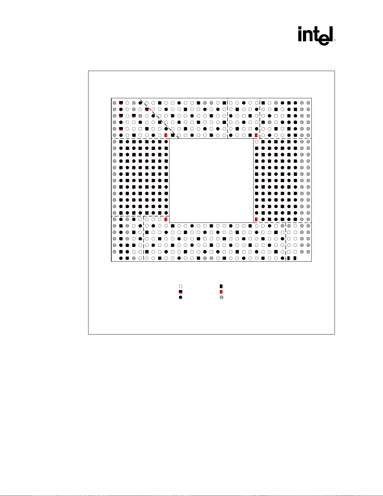
Component Layout
R
Figure 2. TOP VIEW—Intel
COMMON
CLOCK
3 5 7 9 11 13 15 17 19 21 23 25 27 29 31
1
A
B
C
D
E
F
G
H
J
K
L
M
N
P
Vcc / Vss
R
T
U
V
W
Y
AA
AB
AC
AD
AE
4 6
2
®
Xeon™ Processor Socket Quadrant Layout
ADDRESS
COMMON
CLOCK
Xeon™
Processor
Top View
8 10 12 14 16 18 20 22 24 26 28
DATACLOCKS SMBus
Async /
JTAG
A
B
C
D
E
F
G
H
J
Vcc / Vss
K
L
M
N
P
R
T
U
V
W
Y
AA
AB
AC
AD
AE
38 Intel
= Signal
= Power
= Ground = Reserved/No Connect
®
Xeon™ Processor and Intel® 860 Chipset Platform Design Guide
= SM_VCC
= GTLREF
Processor_Socket_Quad_860

Component Layout
A
A
A
A
A
A
A
A
A
A
A
A
R
Figure 3. TOP VIEW—Intel
COMMON
CLOCK
3 5 7 9 11 13 15 17 19 21 23 25 27 29 31
1
B
C
D
E
F
G
H
J
K
L
M
N
Vcc / Vss
P
R
T
U
V
W
Y
A
B
C
D
E
4 6
2
CLOCKS
®
Xeon™ Processor with 512 KB L2 Cache Socket Quadrant Layout
ADDRESS
COMMON
CLOCK
Async /
JTAG
B
C
D
E
F
G
H
J
Xeon™
Processor
with 512 KB L2 Cache
Top View
8 10 12 14 16 18 20 22 24 26 28
= Signal
= Power
= Ground
DATA
= SM_VCC
= GTLREF
= Reserved
SMBus
Processor_Socket_Quad_Cache_860
K
L
M
N
P
R
T
U
V
W
Y
A
B
C
D
E
Vcc / Vss
®
Xeon™ Processor and Intel® 860 Chipset Platform Design Guide 39
Intel

Component Layout
2.2 Intel® 860 Chipset Component Quadrant Layout
Figure 4 through Figure 7 illustrate the quadrant layouts for the Intel 860 chipset components. In
the event that information in a component datasheet and this information conflict, the information
in the datasheet supercedes.
Figure 4. TOP VIEW—MCH Quadrant Layout
AGP
R
RAC B
Interface B
Hub
Hub
Interface A
Figure 5. TOP VIEW—Intel® ICH2 Quadrant Layout
Hub Interface
LAN
ICH2
360-Ball
EBGA
MCH
OLGA
RAC A
CPU
System Bus
Hub
Interface C
IDE
AC’97 SMBus
LPC
40 Intel
PCI USB
®
Xeon™ Processor and Intel® 860 Chipset Platform Design Guide

Component Layout
R
Figure 6. TOP VIEW—Intel
®
P64H Quadrant Layout
PCI
P64H
241-Ball
µBGA* CSP
Figure 7. TOP VIEW— Intel® MRH-R Quadrant Layout
Clocks / Miscellaneous
Hub Interface
Interrupt
Rambus* Channel B
Interface
(Master Interface)
®
Xeon™ Processor and Intel® 860 Chipset Platform Design Guide 41
Intel
MRH-R
324-Ball
µBGA* CSP
Expansion Channel
(Slave Channel)
Rambus Channel A
Interface
(Master Interface)
quadrant_mrh-r

Component Layout
This page is intentionally left blank.
R
®
42 Intel
Xeon™ Processor and Intel® 860 Chipset Platform Design Guide

Platform Stack-Up and Placement Overview
R
3 Platform Stack-Up and Placement
Overview
3.1 Platform Component Placement
The following figures illustrate general component placement for workstation systems. The
assumptions used for the component placement are described in the following table.
Table 6. Placement Assumptions for Workstation Configurations
Assumptions
System
Configuration
Workstation (DP) Extended-ATX/Entry SSI 8 Layers Single Sided
Form Factor Number of Total PCB Layers Assembly
®
Xeon™ Processor and Intel® 860 Chipset Platform Design Guide 43
Intel

Platform Stack-Up and Placement Overview
Figure 8. DP Workstation Component Placement Example in an Extended ATX Form Factor
R
®
44 Intel
Xeon™ Processor and Intel® 860 Chipset Platform Design Guide

Platform Stack-Up and Placement Overview
R
3.2 Two-Way System Stack-Up
Design recommendations are presented first in this section, followed by design considerations.
3.2.1 Design Recommendations
3.2.1.1 Stack-Up Option A
A dual processor motherboard stack-up option is shown in Figure 9. Signal layers should be routed
as unbalanced stripline referencing layers 2 and 5 only. Stripline routing has fewer mode
dependent velocity changes and results in less system timing skew than microstrip. For signals
other than the system bus source-synchronous AGTL+ signals, layers 0 and 7 also provide routing
room in the presence of surface mount devices, such as the processor sockets. Layers 0 and 7
should not act as reference planes for the system bus signals.
The separations between layers 0 and 1, layers 3 and 4, and layers 6 and 7 should be kept as large
as possible. Therefore, the distance between the signal trace and the reference plane should be
greater than 1.8x for layers 0 and 1 and layers 6 and 7 (where x is the distance between layers 1
and 2, 2 and 3, 4 and 5, 5 and 6). A distance greater than 3x should be kept between signals on
layers 3 and 4. In addition, signals on layers 3 and 4 should be routed orthogonal to each other.
Figure 9. Eight Layer Stack-Up for DP Configurations—Option A
Gnd Plane
Not Used As A
Referenc e Plan e
Layer 1
Pwr Plane
Layer 3
Used As A
Reference Plane
Layer 4
Gnd Plane
Layer 6
Pwr Plane
x
x
x
x
>1.8x
>3x
>1.8x
Layer 0
Layer 2
Layer 5
Layer 7
8 Layer Stack A
Signal
Signal
Signal
Signal
®
Xeon™ Processor and Intel® 860 Chipset Platform Design Guide 45
Intel

Platform Stack-Up and Placement Overview
3.2.1.2 Stack-Up Option B
Stack-up option B shown in Figure 10 has the advantage of using symmetric stripline routing
preferred for the system bus on layer 2 and layer 5. However, it uses microstrip routing on layer 0
and layer 7. Microstrip routing is worse than the stripline routing of Option A in that it is more
susceptible to variations in fab manufacturing and crosstalk. Furthermore, microstrip has a
different propagation delay, which must be accounted for in flight time simulations. If Option B is
used, all 4X signals must be routed on layer 2 and layer 5. 2X signals should also be routed on the
symmetric stripline layers (2 & 5), but may be routed on microstrip layers if necessary. Common
clock signals can be routed as microstrip. It is important to prevent layer switching, particularly
between stripline and microstrip layers. BCLK signals should be routed on stripline layers. Any
signals routed as microstrip must account for the increased crosstalk coefficient, the difference in
flight time, and the effect of greater fab variation on skew.
Figure 10. Eight Layer Stack-Up for DP Configurations—Option B
R
Layer 0
Gnd Plane
Layer 2
Pwr Plane
Pwr Plane
Layer 5
Gnd Plane
Layer 7
3.2.2 Design Considerations
The following design considerations are based on Intel reference designs for the Intel Xeon
processor and Intel Xeon processor with 512 KB L2 cache with the Intel 860 chipset. These
designs are targeted to provide a high quality platform with optimized signal integrity, timing
margins, and power distribution. These design considerations represent Intel’s recommended
platform design. However, excursions from these guidelines can be made to optimize for cost or
system-specific designs without violating the specifications of either the processor or chipset. In
any design it is up to the designers to ensure that the platform meets all the component
specifications. Intel strongly recommends that a comprehensive simulation analysis be performed
to ensure all such specifications will be met. This is particularly important for designs that deviate
from the following design considerations.
Layer 1
Layer 3
Layer 4
Layer 6
Signal
Signal
Signal
Signal
8 Layer Stack B
®
46 Intel
Xeon™ Processor and Intel® 860 Chipset Platform Design Guide

Platform Stack-Up and Placement Overview
R
3.2.2.1 Stack-Up Example A
Use the following items and the stack-up in Figure 11 as the design considerations for the dual
processor system stack-up Example A.
• 1 oz. Copper in middle layers.
• There must be the equivalent total of at least 2 oz. Of copper on power planes for power
delivery to the processor.
• Vias are 10 mil holes with 35 mil anti-pads (24 mil pads).
• Total board thickness is 0.0685 inches. (Slightly greater than the preferred standard
0.062 inch).
Figure 11. Dual Processor Stack-Up Example
FR4 Thickness:
10.5 mil
5.5 mil
4.8 mil
15.4 mil
4.8 mil
5.5 mil
10.5 mil
Copper Thickness:
Gnd Plane (1.5 oz. cu.)
Signal Layer (1 oz. cu.)
Power Plane (1 oz. cu.)
Signal Layer (1 oz. cu.)
Signal Layer (1 oz. cu.)
Gnd Plane (1 oz. cu.)
Signal Layer (1 oz. cu.)
Power Plane (1.5oz. cu.)
®
Xeon™ Processor and Intel® 860 Chipset Platform Design Guide 47
Intel

Platform Stack-Up and Placement Overview
3.2.2.2 Stack-Up Example B
Use the following items and the stack-up in Figure 12 as the design considerations for the dual
processor system stack-up Example B. For detailed thickness information, refer to Figure 13.
• A system bus impedance of 50 Ω can be obtained with 5 mil traces for stripline and 7 mil
traces for microstrip.
• There must be the aggregate total of at least 2 oz of copper on power and ground planes for
power delivery to the processor.
• Vias are 10 mil hole with a 32 mil anti-pad (24 mil pad)
• Total board thickness is 0.062 inches.
Figure 12. Dual Processor Example Stack-Up B
R
FR4 Thickness:
4.0 mil
7.0 mil
6.5 mil
14.0 mil
6.5 mil
7.0 mil
4.0 mil
Copper Thickness:
Signal Layer (plated 1/2 oz. cu.)
Gnd Plane (1 oz. cu.)
Signal Layer (1 oz. cu.)
Power Plane (1 oz. cu.)
Power Plane (1 oz. cu.)
Signal Layer (1 oz. cu.)
Gnd Plane (1 oz. cu.)
Signal Layer (plated 1/2 oz. cu.)
Stackup_Exmpl_DP
®
48 Intel
Xeon™ Processor and Intel® 860 Chipset Platform Design Guide
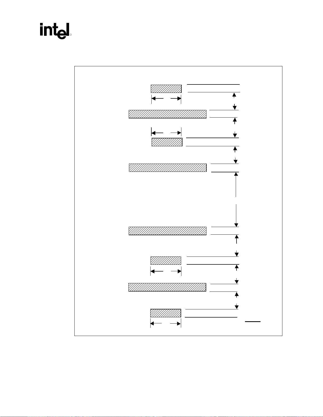
Platform Stack-Up and Placement Overview
R
Figure 13. Stack-Up Example B Thickness Summary
Thickness
(mils)
Top - Signal
(Plated 1 /2oz C u)
L2 - Ground
(Unplated 1oz Cu)
L3 - Signal
(Unplated 0.5 oz Cu)
L4 - Power
(Unplated 1oz Cu)
Core
L5 - Power
(Unplated 1oz Cu)
2.1 mils
A
1.4 mils
C
D
2.1
4
1.4
7
B
0.7 mils
E
1.4 mils
1.4 mils
0.7
6.5
1.4
F
14
1.4
G
6.5
L6 - Signal
(Unplated 0.5 oz Cu)
L7 - Ground
(Unplated 1oz Cu)
Bot - Signal
(Plated 1/2oz Cu)
0.7 mils
B
1.4 mils 1.4
2.1 mils 2.1
0.7
7
H
4
I
A
Total
®
Xeon™ Processor and Intel® 860 Chipset Platform Design Guide 49
Intel
60.2 mils

Platform Stack-Up and Placement Overview
This page is intentionally left blank.
R
®
50 Intel
Xeon™ Processor and Intel® 860 Chipset Platform Design Guide
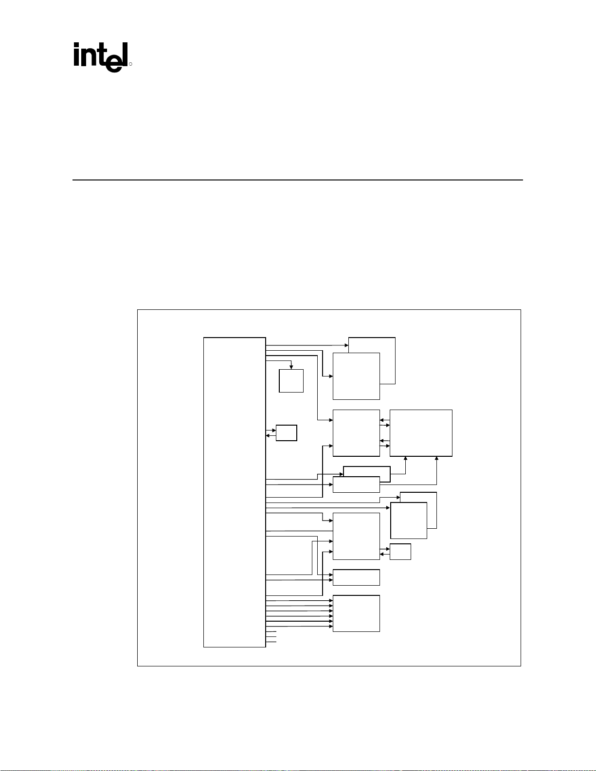
Platform Clock Routing Guidelines
R
4 Platform Clock Routing
Guidelines
Intel recommends CK00 compliant clock drivers for this platform. For more information on CK00
compliance, refer to the CK00 Clock Synthesizer/Driver Design Guidelines.
The CK00 design guidelines specify the following platform clocking solution that can be used with
this Intel 860 chipset-based design.
The clock synthesizer solution is defined in the CK00 guidelines and is shown in the following
figure.
Figure 14. Platform Clocking Architecture Using the CKx_SKS
CKx_SKS
HOST/HOST#
HOST/HOST#
HOST/HOST#
HOST/HOST#
3VMref#
3VMref
3V66
3V66
3V66
3V66
48MHz
48MHz
Ref
Ref
PCI
PCI
PCI
PCI
PCI
PCI
PCI
PCI
PCI
PCI
Debug
Port
XTAL
Processor (s)
MCH
DRCG
DRCG*
Device
ICH2
SIO
PCI
Components/
Slots
Main
Memory
P64H,
H66, or
AGP
32 kHz
XTAL
Clk_Arch_860
®
Xeon™ Processor and Intel® 860 Chipset Platform Design Guide 51
Intel

Platform Clock Routing Guidelines
4.1 Routing Guidelines for Host Clocks
The CKx_SKS clock synthesizer provides four sets of 100 MHz differential clock outputs. The
100 MHz differential clocks are driven to the processors and MCH as shown in Figure 15.
Figure 15. Dual Processor BCLK Topology
R
T
R
S
R
S
R
T
Processor
R
Clock Driver
CKx_SKS
R
T
R
S
R
S
R
T
R
T
R
S
R
S
R
T
R
T
R
S
R
S
R
T
Processor
MCH
Debug Port
NOTE: Connect the CK00 component's HOST pin to the BCLK0 pins on the processor and MCH.
Additionally, connect the CK00 HOST _BAR pin to the BCLK1 pins. For production boards, the debug port can
be removed and the unused host clocks can be terminated to GND via 10K Ohm resistors.
BCLK_Topo
®
52 Intel
Xeon™ Processor and Intel® 860 Chipset Platform Design Guide
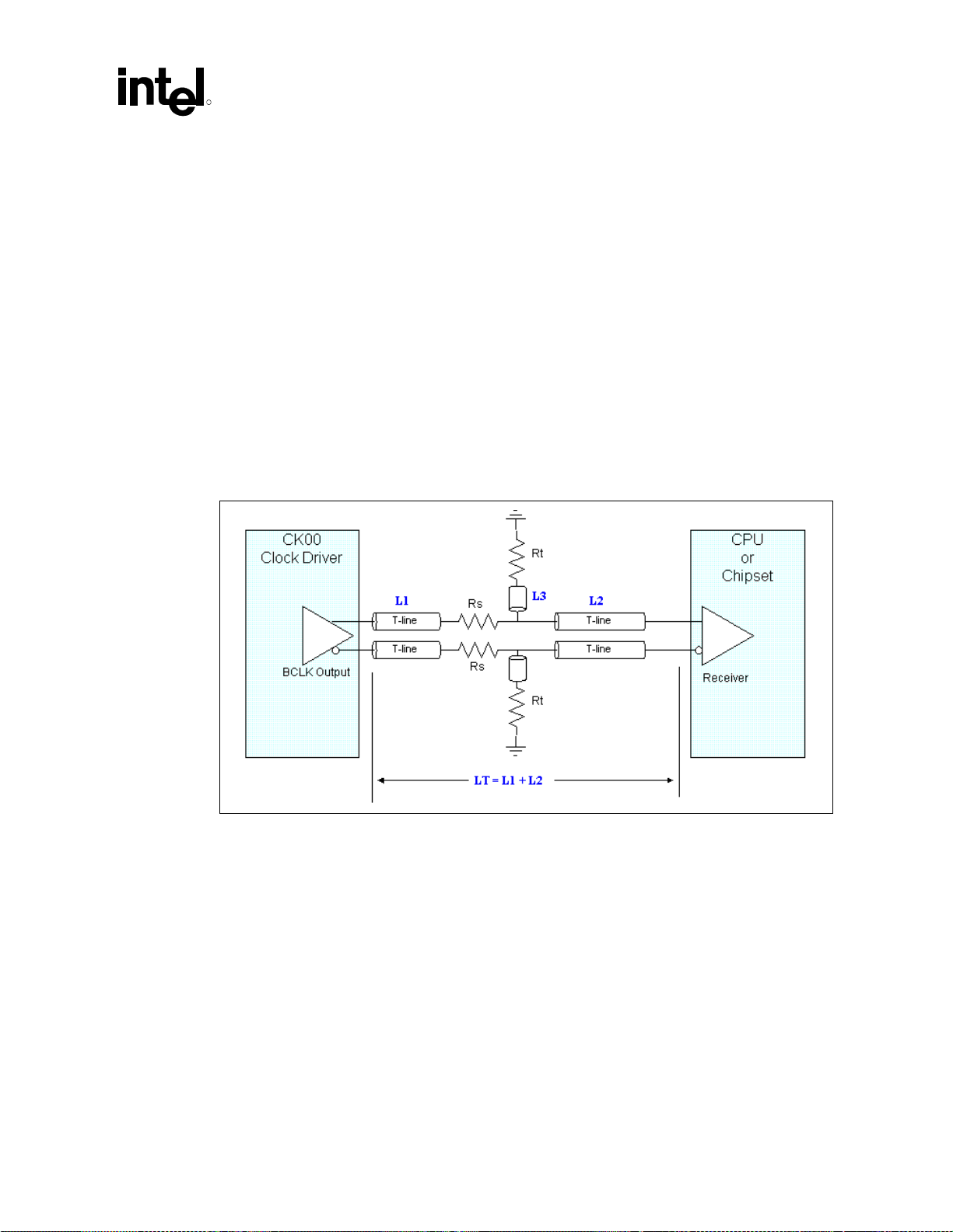
Platform Clock Routing Guidelines
R
The CK00 clock driver’s differential bus output structure is a “Current Mode, Current Steering”
output that develops a clock signal by alternately steering a programmable constant current to the
external termination resistors R
The current I
is programmable by a resistor and an internal multiplication factor so the
OUT
amplitude of the clock signal can be adjusted for different values of R
. The resulting amplitude is determined by multiplying I
T
for impedance matching or
T
OUT
by RT.
to accommodate future load requirements. Refer to the CK00 Clock Synthesizer/Driver Design
Guidelines for more detailed information.
The recommended termination for the CK00 differential bus clock is a “Shunt Source
termination”. Refer to Figure 16. Parallel resistors R
perform a dual function: converting the
T
current output of the CK00 to a voltage, and matching the driver output impedance to the
transmission line. The series resistors R
parasitics, which would otherwise appear in parallel with the termination resistor R
provide isolation from the clock driver’s output
S
T
The value of R
R
should be between 20 and 33 Ω. Simulations have shown that RS values above 33 Ω provide no
S
should be selected to match the characteristic impedance of the motherboard, and
T
benefit to signal integrity, but do degrade the edge rate.
Figure 16. Source Shunt Termination
The goal of constraining all bus clocks to one physical routing layer is to minimize the impact on
skew due to variations in ε
, and the impedance variations due to physical tolerances of circuit
r
board material. Routing on internal layers provides the least amount of ε
• Requirement: Do not split up the two halves of a differential clock pair between layers.
and impedance variation.
r
• Goal: Route clocks to all agents on same physical routing layer.
®
Xeon™ Processor and Intel® 860 Chipset Platform Design Guide 53
Intel

Platform Clock Routing Guidelines
General Routing Guidelines:
• If layer transition is required, make sure that skew induced by the vias used to transition
between routing layers is compensated in the traces to other agents.
• Layer transitions should only be made between routing layers of the same configuration (i.e.,
stripline layer to stripline layer).
R
• Keep routes to all agents as short as possible to minimize the cumulative effects of ε
r
variations on clock skew.
• Do not place Vias between adjacent complementary clock traces.
• Avoid differential Vias. A via that’s placed in one half of a differential pair must be matched
by a via in the other half. Can have differential vias within length L1, between clock driver
and RS, if needed to shorten length L1.
EMI Constraints:
Clocks are a significant contributor to electro-magnetic interference (EMI) and should be treated
with care. The following recommendations can aid in EMI reduction:
• Route clocks on inner layers.
• On internal signal layers maintain a minimum of 100 mils from the edge of the clock traces to
the edge of the motherboard.
• Maintain uniform spacing between the two halves of differential clocks.
• Route clocks on physical layer adjacent to the VSS reference plane only.
The following table describes the routing guidelines for the bus clock signals.
®
54 Intel
Xeon™ Processor and Intel® 860 Chipset Platform Design Guide

Platform Clock Routing Guidelines
R
Table 7. BCLK[1:0]# Routing Guidelines Summary
Layout Guideline Value Figures Notes
BCLK Skew between agents 200 ps total
150 ps for Clock driver
100 ps for interconnect
Differential pair spacing 4 x W min. to 5 x W max. Figure 18 4, 5
Spacing to other traces 25 mils Figure 18
Serpentine spacing Maintain a minimum S/h ratio of > 5/1
Keep parallel serpentine sections as short as
possible
Minimize 90
possible.
Line width 4.0 mil typical 6
Motherboard Impedance–
Differential
Motherboard Impedance–
single ended
Processor routing length–
L1: CK_WBY/CK_SKS to Rs
Processor routing length–
L2: Rs to Processor
MCH routing length–
L1: CK_WBY/CK_SKS to Rs
MCH routing length–
L2: Rs to Processor
L3: Stub length to Rt Stubless
Processor to CS length
matching (LT)
Processor to Processor length
matching (LT)
BCLK0–BCLK1 length
matching
Rs Series termination value 33 Ω ± 5% Figure 16 11
Rt Shunt termination value 49.9 Ω ± 1% Figure 16 12
100 Ω typical 7
50 Ω ± 10% 8
0.5 inch max Figure 16
0 inch–12 inches Figure 16
0.5 inch max Figure 16
0 inch–12 inches Figure 16
10 mils max from via to pad
0.3 inch ± 0.010 inch
MCH LT must be 0.3 inch longer than
Processor LT.
± 10 mils Figure 16 10
± 10 mils
° bends. Make 45° bends if
Figure 17 1, 2, 3
Figure 18
Figure 16
Figure 16 9
NOTES:
1. The skew budget includes clock driver output pair to output pair jitter (differential jitter), and skew, clock
skew due to interconnect process variation, and static skew due to layout differences between clocks to
all bus agents. This number does not include clock driver common mode (cycle to cycle) jitter, or spread
spectrum clocking.
2. This number assumes all BCLK pairs are routed on the same signal layer.
3. Skew measured at the load between any two bus agents. Measured at the crossing point.
4. Edge-to-edge spacing between the two traces of any differential pair. Uniform spacing should be
maintained along the entire length of the trace.
®
Xeon™ Processor and Intel® 860 Chipset Platform Design Guide 55
Intel

Platform Clock Routing Guidelines
5. Clock traces are routed in a differential configuration. Maintain the minimum recommended spacing
between the two traces of the pair. Do not exceed the maximum trace spacing because this will degrade
the noise rejection of the network.
6. Set trace width to meet correct motherboard impedance. The value for trace width provided here is a
recommendation on how to meet the proper trace impedance based on the recommended stack-up.
7. The differential impedance of each clock pair is approximately 2*Zsingle-ended*(1-2*Kb) where Kb is
the backwards crosstalk coefficient. For the recommended trace spacing, the Kb is very small and the
effective differential impedance is approximately equal to 2 times the single-ended impedance of each
half of the pair.
8. The single ended impedance of both halves of a differential pair should be targeted to be of equal value.
They should have the same physical construction. If the BCLK traces vary within the tolerances
specified, both traces of a differential pair must vary equally.
9. Length compensation for the processor socket and package delay is added to chipset routing to match
electrical lengths between the chipset and the processor at die pad. Therefore, the motherboard trace
length for the chipset will be longer than that for the processor.
10. Length of LT for one processor must match the LT of all other BCLK traces to other processors with
specified tolerance.
11. Rs values of 20
Ω–33 Ω have been found to be effective. The value specified is the recommended
value.
12. Rt values should match the motherboard trace impedance for BCLK.
Figure 17. Clock Skew as Measured from Agent-to-Agent
R
Figure 18. Trace Spacing
BCLK1
Agent 0
BCLK0
Agent 0
BCLK1
Agent 1
BCLK0
Agent 1
S2
H
Tclkskw
S1
W
clk_skew_860
S2
56 Intel
Trace_Space_860
®
Xeon™ Processor and Intel® 860 Chipset Platform Design Guide
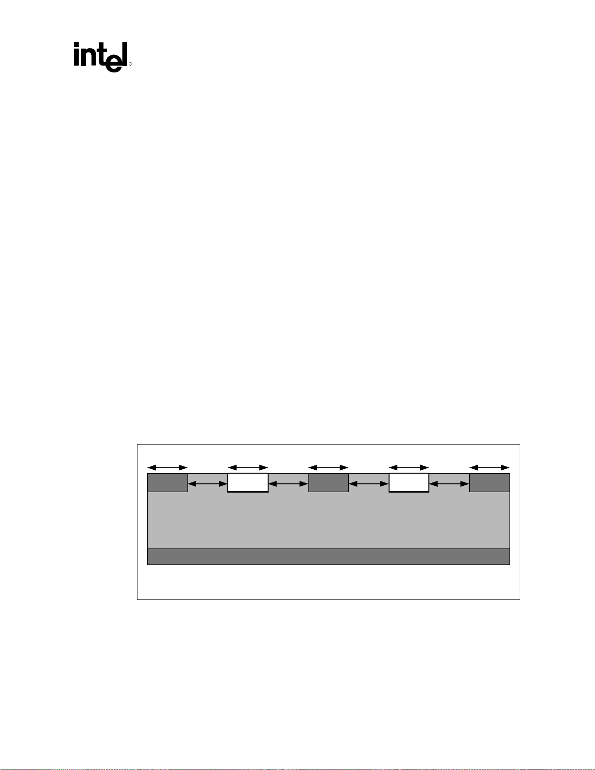
Platform Clock Routing Guidelines
R
4.2 Routing Guidelines for Direct Rambus* Clock Generators (DRCG Devices)
The CKx_SKS clock synthesizer provides two 3.3 V clock reference outputs [3 Vmref and
3 Vmref#] that are used by the Direct Rambus Clock Generators (DRCG devices). Two DRCG
devices are required in an Intel 860 chipset dual Rambus Channels interface.
These reference clocks operate at one-half the host clock frequency. They are inputs into the
DRCG devices and are used to generate the Direct Rambus* Clock Generator “Clock-to-Master”
differential pair (CTM, CTM#).
In addition, the DRCG device uses phase information provided by the MCH via the RCLKOUT
and HCLKOUT phase aligning clock signals. This phase alignment information is sent to the
DRCG SYNCLKN and PCLKM pins from MCH RCLK and HCLK.
4.2.1 CKx_SKS to DRCG: Reference Clocks
The 3VMRef clock output must be routed as shown in Figure 19. Note that the VddIR power pin
on the DRCG device can be connected directly to 3.3 V near the DRCG device if the 3.3 V plane
extends near the DRCG device. However, if a 3.3 V trace must be used, it should originate at the
clock synthesizer and be routed as shown. The maximum length for the 3VMRef and 3VMRef#
signals is 8 inches.
Note: The following recommendations assume routing of the reference clocks on microstrip.
Figure 19. VddIR and 3VMRef or 3VMRef# Routing
6 mils
GROUND
6 mils
6 mils
VddIR
6 mils
GROUND
6 mils
GROUND/POWER PLANE
6 mils
6 mils
3VMRef
6 mils
6 mils
GROUND
3VMRef_Clk_Rout
Note: 3VMRef# should be routed in a similar manner as 3 VMRef.
®
Xeon™ Processor and Intel® 860 Chipset Platform Design Guide 57
Intel

Platform Clock Routing Guidelines
4.2.2 MCH to DRCG* Device: Phase Aligning Clocks
The RCLKOUT and HCLKOUT signals from the MCH should be routed to the SYNCLKN and
PCLKM signals on the DRCG device, respectively, as shown in Figure 20. Note that the VddIPD
power pin on the DRCG device can be connected directly to 1.8 V near the DRCG device if the
1.8 V plane extends near the DRCG device. However, if a 1.8 V trace must be run, it should
originate at the MCH and be routed as shown with respect to RCLKOUT and HCLKOUT.
The maximum length for RCLKOUT and HCLKOUT is 6 inches. Additionally, these signals must
be length matched within 50 mils. These signals should be routed on the same layer. If these
signals must switch layers, then BOTH signals should change layers together.
If the VddIPD pin is connected to the 1.8 V plane using a via (i.e., trace is not run from the MCH),
then HCLKOUT and RCLKOUT must still be routed as shown in Figure 20 and ground isolated.
Note: The following recommendations assume routing of the phase alignment clocks on microstrip.
Figure 20. MCH to DRCG* Device Routing Diagram
R
6 mils
GROUND
6 mils
5 mils
VddIPD
6 m ils
6 mils
GROUND
6 mils
GROUND/POWER PLANE
6 mils
Rclkout
12 mils
6 mils
Hclkout
6 mils
GROUND
6 mils
Note: The signals RCLKOUT and HCLKOUT are channel specific, and their exact names are
CHx_RCLKOUT and CHx_HCLKOUT, where x is the channel (either A or B). Consult the Intel
860 Chipset: 82860 Memory Controller Hub (MCH) Datasheet for more information.
4.2.3 DRCG* Device Signals to Rambus* Channels (300 MHz/400 MHz Clocks)
The Direct Rambus* Clock Generator (DRCG device) signals (i.e., CTM/CTM# and CFM/CFM#)
are high-speed, impedance matched transmission lines that require strict routing recommendations
to insure that the memory timings are met. The following DRCG device recommendations should
be strictly followed. Any deviations from the recommendations should be properly simulated.
®
®
58 Intel
Xeon™ Processor and Intel® 860 Chipset Platform Design Guide

Platform Clock Routing Guidelines
R
4.2.3.1 Trace Length Recommendations
Figure 21 shows the critical Direct Rambus Clock Generator routing sections, with the routing
lengths for each section defined in Table 8.
Figure 21. Direct Rambus* Clock Generator Routing Dimension
MCH
C
A
B
Clk_Route_Dim_860
The following table shows the routing length recommendations for the CTM/CTM# and
CFM/CFM# 400 MHz Direct Rambus Clock Generator. Note that the recommendations are shown
for a single Rambus Channel and should be applied to both of the MCH Rambus Channels.
Table 8. Direct Rambus* Clock Generator Routing Guidelines
Clock From To Length (inches) Figure 21
DRCG* Device 2nd RIMM Connector 0.0–6.0 D
CTM/CTM# (1)
CFM/CFM# (2)
NOTES: .
1. First RIMM connector to MCH:
Trace length must be compensated to match the RSL signals from MCH to first RIMM connector.
2. MCH to First RIMM connector:
Trace length must be compensated to match the RSL signals from first RIMM connector to MCH.
RIMM Connector RIMM Connector 0.4–1.0 B
st
RIMM Connector MCH 1.0–6.0 A
1
MCH 1st RIMM Connector 1.0–6.0 A
RIMM Connector RIMM Connector 0.4–1.0 B
nd
RIMM Connector Termination 0.0–2.0 C
2
D
TERM
DRCG*
Device
Trace
In clock routing sections ‘A’ and ‘D’, the clock signals (CTM/CTM# and CFM/CFM#) should be
routed differentially. An example recommended topology for microstrip differential clock routing
is shown in Figure 22.
Note: Clock trace widths and spacing may change according to prepreg thickness.
The clock signals shown in the example topology are 14 mils wide and are routed differentially.
There must be a 22 mil ground isolation trace routed around the clock differential pair signals. The
22 mil ground isolation traces must be connected to ground with a via per every 1 inch. Vias must
be placed within 0.5 inch of the beginning and end of the ground isolation trace. A 6 mil gap is
required between the clock signals, and between the clocks and ground isolation traces.
®
Xeon™ Processor and Intel® 860 Chipset Platform Design Guide 59
Intel

Platform Clock Routing Guidelines
Figure 22. Differential Clock Routing Diagram
22 mils 22 mils14 mils 14 mils
R
GROUND CLOCK CLOCK# GROUND
6 mils 6 mils6 mils
GROUND/POWER PLANE
Diff_Clk_Rout
Note: “CLOCK” stands for the CTM and CFM signals, and “CLOCK#” stands for the CTM# and
CFM# signals.
In clock routing section ‘B’, the CTM/CTM# and CFM/CFM# clock signals should be routed nondifferentially because of the short routing lengths between RIMM connectors. An example
recommended topology for microstrip non-differential clock routing is shown in Figure 23.
Note: Clock trace widths and spacing may change according to prepreg thickness.
The clock signals shown in the example topology are routed with 18 mil wide traces. When
routing the clocks non-differentially, there must be a 10 mil ground isolation trace routed around
the single-ended clock signals. The 10 mil ground isolation traces must be connected to ground
with a via per every 1 inch. Vias must be placed within 0.5 inch of the beginning and end of the
ground isolation trace. A 6 mil gap is required between the clock signals and the ground isolation
traces.
Figure 23. Non-Differential Clock Routing Diagram
10 mils 10 mils
GROUND
Note: “CLOCK” represents the signals CTM, CTM#, CFM and CFM#
6 mils
18 mils
CLOCK GROU ND
GROUND/POWER PLANE
6 mils
Non-Diff_Cl k_Rout
Note: The CTM/CTM# and CFM/CFM# clock signals must be ground referenced (with continuous
ground island/plane) at all times.
®
60 Intel
Xeon™ Processor and Intel® 860 Chipset Platform Design Guide

Platform Clock Routing Guidelines
R
4.2.3.2 Topology Considerations
Package trace compensation, via compensation, and RSL signal layer alteration must also be
considered when routing the Direct Rambus Clock Generator. Additionally, when routing on
microstrip layers, 0.021 inches of CLK per 1 inch of RSL trace length must be added to
compensate for the clock’s faster trace velocity.
For clock routing sections ‘A’ and ‘B’, the CTM/CTM# and CFM/CFM# clocks must be length
matched within ± 2 mils to the RSL channel trace length. Exact matching is preferred.
For trace sections ‘C’ and ‘D’, the CFM/CFM# clocks must be length matched within ± 2 mils to
the RSL channel trace length. Exact matching is preferred.
4.2.3.3 Clock Termination
The CFM/CFM# differential pair signals require termination using either 27 Ω 1% or 28 Ω 2%
resistors and a 0.1 µF capacitor as shown in the following figure.
Figure 24. CFM/CFM# Termination
28 Ω -2%
or
Ω - 1%
27
Ω -2%
28
or
Ω - 1%
27
R1
R2
C1
0.1 uF
CFM_Term
®
Xeon™ Processor and Intel® 860 Chipset Platform Design Guide 61
Intel

Platform Clock Routing Guidelines
4.2.4 DRCG* Device Impedance Matching Circuit
The external DRCG device impedance matching circuit is shown in the following figure.
Figure 25. DRCG* Device Impedance Matching Network
3.3 V
R
To 3.3 V DRCG
Supply
Connection
CH
CH
C
2
Bulk
DRG_Imped_Match_8 60
CD
CD
2
C
D
VDDIR
V
DD
C
D
O
Z
VDDP
C
D
C
D
C
D
V
DD
V
DD
DRCG*
Device
C
IPD
V
O
DD
R
S
C
D
R
S
C
D
R
P
C
MID
R
P
Z
F
Bead
R
T
C
MID2
R
T
®
62 Intel
Xeon™ Processor and Intel® 860 Chipset Platform Design Guide

Platform Clock Routing Guidelines
R
Table 9. DRCG* Device Impedance Matching Network Values
Component Nominal Value Notes
CD 0.1 µF Decoupling caps to GND
R
39 Ω Series termination resistor
S
R
51 Ω Parallel termination resistor
P
C
, C
MID1
R
27 Ω End of channel termination
T
CF 4 pF–15 pF Do Not Stuff, leave pads for future use
Fbead 50 Ω at 100 MHz Ferrite bead
CD2 0.1 µF Additional 3.3 V decoupling caps
Cbulk 10 µF Bulk cap on device side of ferrite bead
NOTES:
1. Note the removal of the original EMI capacitors between the junctions of RS, RP and ground. These
2. The intent of component CF is to decouple CLK and CLKB outputs to each other, but data shows this
3. The ferrite bead and 10 µF bulk cap combination improves jitter and helps to keep the clock noise away
4. 0.1 µF capacitors are better than 0.01 µF or 0.001 µF capacitors for DRCG device decoupling. Most
5. Cmid at 0.1 µF has improved jitter versus Cmid at 100 pF. However, this will increase the latency
6. RS, RP, RT were modified to improve channel signal integrity through increasing CTM/CTMN swing.
7. The circuit shown is required to match the impedance of the DRCG device to the 28
8. The previously recommended 15 pF capacitors on CTM/CTM# should be removed. The 4 pF capacitor
0.1 µF Virtual GND caps
MID2
capacitors had minimal impact on EMI and increased DRCG device output jitter by approximately 2X.
actually increases device jitter. CF should not be stuffed at this time.
from the rest of the system. The additional 3.3 V capacitors (CD2) have a minor positive impact, but the
ideal values have not been extensively optimized.
decoupling experiments that replaced 0.1 µF capacitors with higher frequency caps ended up with the
same or worse jitter. Replacing existing 0.1 µF capacitors with higher frequency capacitors is not
advised.
coming out of a stop clock or tri-state mode.
Ω channel
impedance. More detailed information can be found in the Direct Rambus* Clock Generator
Specification.
shown in Figure 26 should not be stuffed.
®
Xeon™ Processor and Intel® 860 Chipset Platform Design Guide 63
Intel

Platform Clock Routing Guidelines
4.2.5 DRCG* Device Layout Example
Figure 26. DRCG* Device Layout Example
R
Cmid – 100 pF
EMI Cap – 4 pF
(Keep trace from Rs to Rp short)
Decoupling Cap - 0.1µF
(Place VERY Near DRCG*
Device 3. 3 V Pin!)
Decoupling Cap - 0.1 µF
(Place VERY Near DRCG 3.3V Pin! )
Do Not Stuff
Rp – 51 Ω
CTM/CTM# route on
bottom layer
Rs - 39 Ω
(Keep trace from DRCG t o
Rs VERY short)
Decoupling Cap - 0.1 µF
(Place VERY Near DRCG 3.3 V Pin!)
3.3 V DRCG Flood
Flood 3.3 V DRCG on the top layer
around DRCG. Flood MUST
include:
4 DRCG Power Pins
4 0.1 µF Capacitors
1 10 µF Bulk Capacitor
1 Isolation Ferrite Bead
Decoupling Cap - 0.1 µF
(Place VERY Near DRCG 3.3 V Pin!)
Ferrite Bead
Bulk Decoupling Cap – 10 µF
(Place Near DRCG)
®
64 Intel
Xeon™ Processor and Intel® 860 Chipset Platform Design Guide
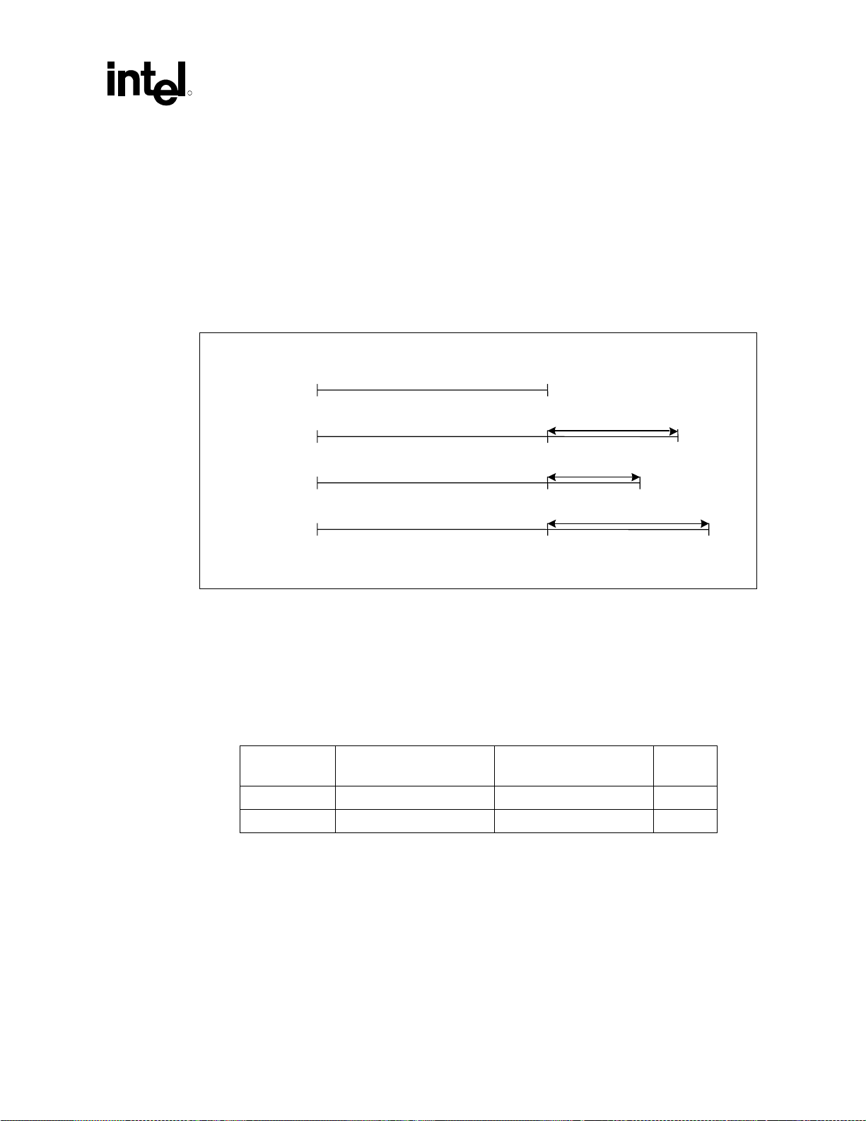
Platform Clock Routing Guidelines
R
4.3 Routing Guidelines for 66 MHz and 33 MHz Clocks
4.3.1 66 MHz/33 MHz Clock Relationships
Figure 27 shows the clock routing relationships between the 66 MHz clocks and the 33 MHz
clocks.
Figure 27. 66 MHz/33 MHz Clock Relationships
AGP_66 to
AGP Slot
CLK_66 to
®
ICH2,
Intel
MCH
PCI_33 to PCI
Slots
CLK_33 to
Intel ICH2,
FWH,
SIO
Z
Z +
Z +
Z +
2.0" - 4.0"
4.3.2 66 MHz Clock Routing Length Guidelines
Table 10 summarizes the layout recommendations between the CK00 clock synthesizer and the
AGP connector, MCH and ICH2 components, which require a 66 MHz clock. Figure 28 and
Figure 29 show traces A and B.
Table 10. 66 MHz Clock Routing Length Guidelines
Clock Group Length of Trace A
(inches)
Length of Trace B
(inches)
4.0" - 5.0"
4.0" - 6.0"
Clk_relationship_66-33
R1 (Ω)
AGP_66 0 to 0.5 Z 33
CLK_66 0 to 0.5 Z + (4 to 5) 33
Note: The routing length value of Z is 5 to 9 inches.
®
Xeon™ Processor and Intel® 860 Chipset Platform Design Guide 65
Intel

Platform Clock Routing Guidelines
Figure 28 and Figure 29 show the recommended clock routing topologies for the 66 MHz clocks.
Figure 28. AGP_66 Clock Routing Topology
R
CK00
Clock
Synthesizer
A
Figure 29. CLK_66 Clock Routing Topology
CK00 Clock
Synthesizer
R1
B
R1
A
B
R1
A B
AGP Connector
AGP-66_Clk_route_860
MCH
ICH2
CLK-66_Clk_route
®
66 Intel
Xeon™ Processor and Intel® 860 Chipset Platform Design Guide

Platform Clock Routing Guidelines
R
4.3.3 33 MHz Clock Routing Length Guidelines
Table 11 summarizes the layout recommendations between the CK00 clock synthesizer and PCI
connectors, ICH2, FWH Flash BIOS and SIO components, which require a 33 MHz clock. Figure
30 and Figure 31 show segments A and B.
Table 11. 33 MHz Clock Routing Guidelines
Clock Group Length of Trace A
(inches)
PCI_33 0 to 0.5 Z + (2 to 4) 33
CLK_33 0 to 0.5 Z + (4 to 6) 33
Note: The routing length value of Z is 5 to 9 inches.
Figure 30 and Figure 31 show the recommended clock routing topologies for the 33 MHz clocks.
Figure 30. PCI_33 Clock Routing Topology
A
A
CK00 Clock
Synthesizer
A
A
A
R1
R1
R1
R1
R1
Length of Trace B
R1 (Ω)
(inches)
B
B
P
C
B
I
B
S
L
B
O
T
P
C
I
S
L
O
T
P
C
I
S
L
O
T
P
P
C
C
I
I
S
S
L
L
O
O
T
T
PCI-33_Clk_route
Figure 31. CLK_33 Clock Routing Topology
R1
A
CK00
Clock
Synthesizer
®
Xeon™ Processor and Intel® 860 Chipset Platform Design Guide 67
Intel
R1
A
R1
A
B
B
B
ICH2
FWH
SIO
clk-33_clk_r oute_860
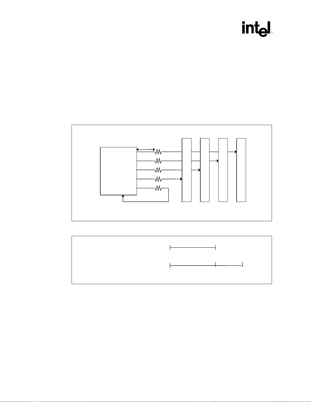
Platform Clock Routing Guidelines
X
X
4.3.4 Intel® P64H PCI Clock Routing Guidelines
4.3.4.1 Intel® P64H PCI 33 MHz Clock Routing Guidelines
At 33 MHz, the P64H can support 4x33 MHz PCI slots. The P64H can provide 6 copies of the
PCLKOUT to PCI devices on its primary PCI bus. PCLKFBOUT is used as the feedback clock
and must be routed into PCLKFBIN of the P64H. The PCLKOUT routing guidelines are shown
below:
R
Figure 32. Intel
®
P64H PCI 33 MHz Clock Routing
1" max
P64H
PCLKFBOUT
PCLKFBIN
Figure 33. Intel® P64H PCI 33 MHz Clock Routing
33
33
33
33
33
P64H PCLKOUT to PCI Slots
P64H Feedback Clock
Ω
Ω
Ω
Ω
Ω
P
C
I
S
L
O
T
P
C
I
S
L
O
T
P
C
I
S
L
O
T
P64H_PCI_33Clk_Rt_860
P
C
S
L
O
T
I
2.5 inches
P64H_PCI_33Clk_Rt2_860
As required by the PCI Specification, the PCI CLK signal length from the expansion board edge
connector to the PCI device should be 2.5 inches ± 0.1 inches for 32-bit and 64-bit expansion
boards.
®
68 Intel
Xeon™ Processor and Intel® 860 Chipset Platform Design Guide

Platform Clock Routing Guidelines
X
X
X
R
4.3.4.2 Intel® P64H PCI 66 MHz Clock Routing Guidelines
At 66 MHz, the P64H can supports 2X66 MHz PCI slots and 1x66 MHz device down. The P64H
can provide 3 copies of the PCLKOUT to PCI devices on its primary PCI bus. PCLKFBOUT is
used as the feedback clock and must be routed into PCLKFBIN of the P64H. The PCLKOUT
layout guidelines are shown in the following figures.
Figure 34. Intel
®
P64H PCI 66 MHz Clock Routing
P64H
PCLKFBOUT
PCLKFBIN
Figure 35. 66 MHz PCI Clock Routing
P64H PCLKOUT to PCI Device (down)
P64H PCLKOUT to PCI Slots
P64H Feedback Clock
1" max
33
33
33
33
Ω
Ω
Ω
Ω
P
C
I
S
L
O
T
P
C
I
S
L
O
T
P64H_PCI_66Clk_Rt_860
PCI
Device
2.5 inches
2.5 inches
P64H_PCI_66Clk_Rt2_860
As required by the PCI Specification, the PCI CLK signal length from the expansion board edge
connector to the PCI device should be 2.5 inches ± 0.1 inches for 32-bit and 64-bit expansion
boards.
®
Xeon™ Processor and Intel® 860 Chipset Platform Design Guide 69
Intel

Platform Clock Routing Guidelines
This page is intentionally left blank.
R
®
70 Intel
Xeon™ Processor and Intel® 860 Chipset Platform Design Guide

System Bus Routing
R
5 System Bus Routing
Table 12 summarizes the layout recommendations for dual-processor based configurations. It
should be used for quick reference only. The subsequent sections in this chapter provide more
detailed information about various system configurations.
Table 12. System Bus Routing Summary
Parameter Guidelines
Line to line
spacing
Data line lengths
(agent-to-agent
spacing)
DSTBn/p[3:0]# line
lengths
Address line
lengths
ADSTB[1:0]# line
lengths
Common Clock
signal line lengths
Topology • Daisy chain with chipset at one end. The end processor must have on-die
Routing priorities • No motherboard contribution to stub length of middle processor (35 mil max trace
Reference plane
requirements
Serpentine
spacing
Motherboard
Impedance
• Greater than 3:1 edge-to-edge spacing vs. trace to reference plane height ratio.
• 3.0 inches to 10.1 inches pin-to-pin.
• Total bus length must not exceed 20.2 inches.
• Data signals within a source synchronous strobe group should be routed within
25 mils of each other, pad to pad.
• Length must be added to the motherboard trace between agents to compensate
for the stub created by the processor package. See section 5.4.1 for details.
• DSTB# signals should follow the same routing rules at the data signals.
In addition:
• The lengths of each DSTBp# and DSTBn# pair should be routed within 25mils of
each other, pad-to-pad, agent-to-agent and over the entire length of the bus.
• A 25 mil spacing should be maintained around each strobe signal (between
DSTBp# and DSTBn#, and any other signal).
• Address signals should follow the same routing rules at the Data signals.
• The lengths of Address signals within a group should be routed within 50 mils of
each other, pad to pad.
• ADSTB# signals should follow the same routing rules at the DSTBn/p[3:0]#
signals.
• Common Clock signals should follow the same routing rules as the Data signals,
however no length compensation is necessary.
termination enabled. No stubs.
via to pad).
• Strobes and associated signals must be routed on same layer for entire length of
bus.
• Avoid changing layers when routing system bus signals. If a layer change must
occur, use vias connecting the VCC_CPU planes and/or VSS planes to provide a
low impedance path for the return current. Vias should be as close as possible to
the signal via.
• S/H greater than or equal to 5 (Figure 36).
• Keep parallel sections as short as possible.
• No 90° bends, use 45° bends whenever possible.
• 50 Ω ± 10%
®
Xeon™ Processor and Intel® 860 Chipset Platform Design Guide 71
Intel

System Bus Routing
5.1 Return Path
The return path is the route current takes to return to its source. It may take a path through ground
planes, power planes, other signals, or integrated circuits. The return path is based on electromagnetic field effects. It is useful to think of the return path as the path of least impedance nearest
the signal conductor. Discontinuities in the return path often have signal integrity and timing
effects that are similar to the discontinuities in the signal conductor. Therefore, the return paths
must be given similar considerations. A simple way to evaluate return path parasitic inductance is
to draw a loop that traces the current from the driver through the signal conductor to the receiver,
and then back through the ground/power plane to the driver again. The smaller the area of the
loop, the lower the parasitic inductance.
The following sets of return path rules apply to all designs:
• Always trace out the return current path and provide as much care to the return path as the
path of the signal conductor.
• Do not allow splits in the reference planes in the path of the return current.
• Do not allow routing of signals on the reference planes near system bus signals.
R
• Do not make signal layer changes that force the return path to make a reference plane change,
even if it is from one VSS layer to another VSS layer.
• Decoupling capacitors do not adequately compensate for a plane split.
• Do not route over via anti-pads or socket anti-pads
If reference plane changes must be made:
• Change from a VSS reference to a VSS reference and place a via that connects the two planes
as close as possible to the signal via. This also applies when making a change from
VCC_CPU to VCC_CPU.
• For symmetric stripline, return path vias for both VSS and VCC_CPU must be provided.
• Do not switch reference from VCC_CPU to VSS or vice versa.
®
72 Intel
Xeon™ Processor and Intel® 860 Chipset Platform Design Guide
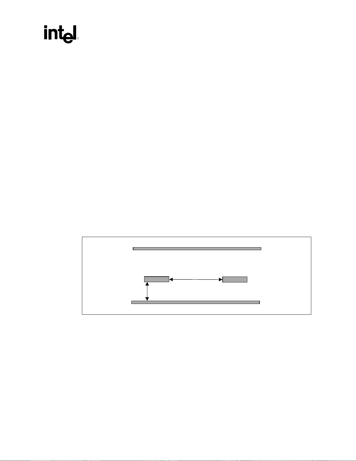
System Bus Routing
R
5.2 Serpentine Routing
A serpentine net is a transmission line that is routed in such a manner that sections of the net
double back and couple to another segment of the same net. Serpentining a transmission line is
sometimes necessary to properly match lengths between nets. It is important to properly control
the serpentine to avoid signal integrity and timing problems. The primary impact of a serpentined
trace is an observed decrease in the flight time when compared to a straight trace of equal length.
This decrease in the flight time is a result of the crosstalk between parallel sections of the
serpentined net. As the signal travels down the transmission line, a component of the signal
follows the transmission line and behaves as though it were a straight line with no serpentine.
However, another portion of the energy propagates perpendicular to the parallel routed portions of
the serpentined net via the mutual capacitance and mutual inductance. This creates an extra mode
that arrives at the receiver significantly earlier than the other component of the signal. If the
coupling between parallel sections is high, significant timing skew can occur when attempting to
match trace lengths on a bus. Furthermore, if the coupling is very high, significant signal integrity
problems can result.
The serpentine guidelines included in this document were based on HSPICE
different spacing between parallel sections. The guidelines were chosen to significantly limit the
effect of serpentining, while minimizing the impact to the application.
Serpentine spacing S/H should be greater than or equal to 5. The S/H ratio is shown in Figure 36.
Figure 36. Serpentine Spacing – Diagram of Spacing to Reference Plane Height Ratio
*
simulations with
S
H
5.3 System Bus Decoupling Requirements
This section contains the motherboard decoupling recommendations to minimize return path
discontinuities and provide necessary power delivery for the bus I/O buffers. These are decoupling
requirements for the system bus I/O only. This decoupling is not adequate for power delivery.
Refer to Section 12.16 for processor core power decoupling requirements.
®
Xeon™ Processor and Intel® 860 Chipset Platform Design Guide 73
Intel

System Bus Routing
µ
5.3.1 Processor I/O Decoupling Requirements
The primary objective of the processor decoupling guidelines is to minimize the impact of return
path discontinuities. The processor power delivery guidelines for the help ensure that the I/O has
adequate power decoupling. The worst-case return path discontinuity anticipated is for systems
that use microstrip structures on the motherboard. The processor, from die to package pin, follows
a symmetric stripline configuration with VCC_CPU as one reference plane, and VSS as the other
reference plane. If the motherboard uses symmetric stripline with VCC_CPU and VSS references,
then a discontinuity does not exist and additional decoupling is not necessary. If the motherboard
routing references only a single reference plane (VCC_CPU or VSS), then a return path
discontinuity exists between the processor and the motherboard, and I/O decoupling capacitors are
required.
The following are decoupling recommendations for each processor (also refer to Figure 37):
• 4 minimum, 6 preferred 0.1 µF capacitors with 603 packages distributed evenly over the
system bus data signals
• 3 minimum, 4 preferred 0.1 µF capacitors with 603 packages distributed evenly over the
system bus address and Common Clock signals
R
• All capacitors placed as close to the processor package as keepout zones allow
Figure 37. I/O Decoupling Guidelines for the Processor
4-6 0.1
F with 603 body
over the data signals and
as close to the processor
package as possible.
Cavity Under
Processor
Data Field
Address and
Control Field
3-4 0.1 µF with 603 body
over the address and
control signals and as close
to the processor package as
Possible.
Proc_ Decouple_E xa
®
74 Intel
Xeon™ Processor and Intel® 860 Chipset Platform Design Guide

System Bus Routing
R
5.4 Dual Processor Configuration
This section provides more details for dual processor based systems. Both recommendations and
considerations are presented.
For proper processor operation, it is necessary to meet the timing and voltage specifications of
each component on the system bus. The most accurate way to understand the signal integrity and
timing of the system bus on the platform is to perform a comprehensive simulation analysis. It is
possible that adjustments to trace impedance, line length, termination impedance, board stack-up,
and other parameters can be made that improve system performance. The following
recommendations are Intel’s best guidelines based on extensive simulation and experimentation
based on our reference platform. It is therefore strongly recommended that you perform a
simulation analysis based on your platform
The following table lists all signals that interface with the processor. This table is a copy of the
table from the processor datasheets referenced in Section 1.1. In the event that this layout conflicts
with the datasheet, the datasheet data supercedes this data.
®
Xeon™ Processor and Intel® 860 Chipset Platform Design Guide 75
Intel

System Bus Routing
Table 13. System Bus Signals
Signal Group Type Signals
AGTL+ Common Clock
Input
AGTL+ Common Clock
I/O
AGTL+ Source
Synchronous I/O: 4X
Group
AGTL+ Source
Synchronous I/O: 2X
Group
AGTL+ Strobes Synchronous to BCLK ADSTB[1:0]#, DSTBN[3:0]#, DSTBP[3:0]#
Async GTL+ Input1 Asynchronous A20M#, IGNNE#, INIT#, LINT0/INTR, LINT1/NMI,
Async GTL+ Output1 Asynchronous FERR#, IERR#, THERMTRIP#, PROCHOT#
System Bus Clock Clock BCLK0, BCLK1
TAP Input1 Synchronous to TCK TCK, TDI, TMS, TRST#
TAP Output1 Synchronous to TCK TDO
SMBus Interface1 Synchronous to
Power/Other BSEL[1:0] 5, GTLREF[3:0], COMP[1:0], OTDEN,
Synchronous to BCLK BPRII#, BR[3:1]#
Synchronous to BCLK ADS#, AP[1:0]#, BINIT#3, BNR#3, BPM[5:0]#1,
Synchronous to assoc.
strobe
Synchronous to assoc.
strobe
SM_CLK
RSP#, TRDY#
BR0#, DBSY#, DP[3:0]#, DRDY#, HIT#
LOCK#, MCERR#
D[63:0]#, DBI[3:0]#
A[35:3]#4, REQ[4:0]#
PWRGOOD, SMI#, SLP#, STPCLK#
SM_EP_A[2:0], SM_TS_A[1:0], SM_DAT,
SM_CLK, SM_ALERT#, SM_WP
RESERVED, SKTOCC#, TESTHI[6:0], VID[4:0],
VCC_CPU, SM_VCC, VCCA, VSSA, VCCIOPLL,
VSS, VCCSENSE, VSSSENSE
1,2
, DEFER#, RESET#1, RS[2:0]#,
3
3
, HITM#3,
R
NOTES:
1. These signals do not have on-die termination on the processor. They must be terminated properly on
the motherboard.
2. The Intel Xeon processor and Intel Xeon processor with 512 KB L2 cache only use BR0# and BR1#.
BR2# and BR3# operation is not supported on these processors and these pins must be terminated to
VCC_CPU. Refer to the routing guidelines in Section 5.4.2.5.
3. These signals are “wired-OR” signals and may be driven simultaneously by multiple agents. For further
details on how to implement wired-OR signals, refer to the routing guidelines in Section 5.4.1.4.
4. The value of these pins during the active to inactive edge of RESET# determine processor configuration
options .
5. Bus Select (BSEL)[1:0] are processor output signals that indicate the system bus frequency supported
by the processor. Since this platform is only designed to operate with a 100 MHz system bus clock, use
these output signals is not required. Refer to the
GHz, 2 GHz and 2.2 GHz Datasheet
76 Intel
for more details about BSEL[1:0] operation.
®
Xeon™ Processor and Intel® 860 Chipset Platform Design Guide
Intel® Xeon™ Processor with 512 KB L2 Cache at 1. 8

System Bus Routing
R
5.4.1 Routing Guidelines for Source Synchronous Signals
Design recommendations are presented first, followed by design considerations. The layout
guidelines given in this section are based on specific chipset (I/O buffer, package, and loading)
and motherboard properties. Complete simulation and hardware validation is necessary to ensure a
robust design.
Design Recommendations
The dual processor topology requires that the chipset be at one end of the bus, and that no
motherboard contribution to the stub length of the processor exists in the middle of the bus. A
diagram of the dual processor daisy chain topology is shown in Figure 38.
Figure 38. Dual Processor System Bus Topology
Length L2Length L1
Proc 0
Chip
Set
D1
LC LC D2
Proc 1
Package trace
Motherboard PCB trace
D1 = processor_delta
D2 = cs _delta
LC = length_comp
Dual_Proc_Bus_Top_860
The motherboard trace impedance should be 50 Ω ± 10%. The traces should maintain a greater
than three to one edge-to-edge spacing versus trace to reference plane height ratio (see Figure 39).
As the traces pass through the pin fields of the 603-pin socket and the chipset, the 3:1 requirement
may not be achievable. In these areas where the 3:1 ratio is not possible, the separation should be
maximized and the distance of the violation should be minimized. Specifically, when routing
through the 603-pin socket, expand to a 3:1 ratio whenever possible. Do not keep a tighter spacing
ratio the entire length of the socket. However, do not route through the VCC_CPU and V
field because this also has a great potential for noise coupling. A trace spacing-to-height above
reference plane ratio of 3 to 1 ensures a low crosstalk coefficient. All the effects of crosstalk are
difficult and tedious to simulate. Intel has performed extensive simulation and experimentation on
the effects of crosstalk to more accurately predict these effects. The timing and layout guidelines
for the processor have been created with the assumption of a 3:1 trace spacing to height above
reference plane ratio. A smaller ratio would have a negative impact on both timing and noise
margins because of crosstalk.
SS
pin
®
Xeon™ Processor and Intel® 860 Chipset Platform Design Guide 77
Intel

System Bus Routing
In a dual processor configuration where the stack-up has two signal layers as the middle layers, the
signals in the middle layers should be routed orthogonal to each other. If routing the signals in an
orthogonal manner is not possible, then maximize the distance of separation between these two
layers and route the signals such that they are not routed directly above each other. This
configuration (signal layers with no reference plane separating them) provides the greatest
coupling co-efficient, and thus a higher potential for detrimental crosstalk.
For partially populated systems, the end processor must be populated first. The end processor is
that furthest from the chipset. This effectively leaves only the socket as a stub on the bus for the
unpopulated agents.
Figure 39. Cross Sectional View of 3:1 Ratio for Stripline (Edge-to-Edge Trace Spacing vs.
Trace to Reference Plane Height)
reference plane
x
R
trace
3x
reference plane
trace
It is critical that additional stub length not be added on the motherboard to the middle processor.
Source synchronous groups and associated strobes should be routed on the same layer for the
entire length of the bus. This results in a significant reduction of the flight time skew since the FR4
thickness, trace width, and velocity of the signals will be uniform across a single layer of the stackup. There is no guarantee of a relationship of FR4 thickness, trace width, and velocity between two
layers.
Additionally, changing layers may create a return path discontinuity that often leads to
unpredictable delay push-outs or pull-ins and signal quality problems. Specifically, if via densities
are large and most of the signals switch at the same time, the layer to layer bypass fails to provide
an acceptably short signal return path to maintain timing and noise margins. Experience at Intel
indicates that the magnitude of the uncertainty that occurs with shifting return paths is on the same
order as the data bus cycle time. If layer changes must be made, it is best to change to a routing
layer that references the same VCC_CPU or VSS plane.
To avoid return path discontinuities, traces must be routed with at least 50% of the trace width
directly over a reference plane. This is particularly important when routing next to vias in the
socket pin field.
®
78 Intel
Xeon™ Processor and Intel® 860 Chipset Platform Design Guide

System Bus Routing
R
Table 14. Source Synchronous Signals and the Associated Strobes
Signals Associated Strobe
REQ[4:0]#, A[16:3]# ADSTB0#
A[35:17]# ADSTB1#
D[15:0]#, DBI0# DDSTBP0##, DSTBN0#
D[31:16]#, DBI1# DSTBP1#, DSTBN1#
D[47:32]#, DBI2# DSTBP2#, DSTBN2#
D[63:48]#, DBI3# DSTBP3#, DSTBN3#
5.4.1.1 4X Group (DSTBN[3:0]#, DSTBP[3:0]#, D[63:0]#, DBI[3:0]#):
The distance from the pin of one agent to the pin of the next must be between 3.0 inches and 10.1
inches. Figure 38 illustrates the dual processor daisy chain topology with the chipset at the end.
Total bus length must not exceed 20.2 inches.
5.4.1.1.1 Trace Length Balancing
Length must be added between each agent to compensate for package length differences that exist
within a source synchronous data group. This length compensation results in minimizing the
source synchronous skew that exists on the system bus. Without the length compensation, the
flight times between a data signal and its strobe is different, which results in an inequity between
the setup and hold times. Since the strobe typically has a shorter package length, there is
favoritism toward hold time, and the setup requirement may not be met without length
compensation on the motherboard. Note this will not make the pad-to-pad lengths between all
agents equal in length, but it will balance the strobe-to-signal skew in the middle of the setup-andhold window between all driver-receiver combinations.
Compensating for the processor package lengths on the motherboard is necessary. The amount that
should be added can be calculated using Equation 1. This length should be added to motherboard
trace segment L1.
Equation 1. Processor Package Compensation Length
,
Compensating for the chipset package lengths on the motherboard is also necessary. The amount
that should be added can be calculated using Equation 2. This length should be added to
motherboard trace segment L2.
−==
pkglencpupkglencpudeltacpuD __max__1
netgroupgroupnet
®
Xeon™ Processor and Intel® 860 Chipset Platform Design Guide 79
Intel

System Bus Routing
Equation 2. Chipset Package Compensation Length
R
,
−==
A length of 0.78 times the processor package compensation length (D1) should be added between
each agent. See Equation 3. The length should be added to motherboard trace segment lengths
L1 and L2.
Equation 3. Additional Compensation Length for DP Systems
, netgroupgroupnet
The routed motherboard lengths within a source synchronous group should match the results of the
previous equations to ± 25 mils between agent-to-agent, and ± 50 mils over the entire length of the
bus. This skew should be simulated to determine the length that best centers the strobe for a given
system.
Example Using Hypothetical Numbers
Consider 2 signals, DSTBP0# and D1#, from the same group. Assume that L1 (motherboard trace
from CPU1 to CPU2) for DSTBP0# and D1# is 4 inches. Similarly, assume that the package trace
for DSTBP0# is 0.15 inches (cpu_pkglen) and D1# is 0.35 inch (max_cpu_pkglen). Using
Equation 1, the delta will be 0.20 inches (0.35 – 0.15). Using Equation 3, length_comp for D0 is
0.156 inches 0.78*(0.20). The length-matching spreadsheet therefore requires that additional
length of 0.356 inches (0.20 + 0.156) be added to signal DSTBP0#. Hence, the new length for
DSTBP0# will be 4.356 inches (instead of the current 4 inches). The length matching spreadsheet
requires the new length of DSTBP0# to be within ± 0.025 inches (25 mils) of 4.356 inches.
pkglencspkglencsdeltacsD __max__2
netgroupgroupnet
pkglencpupkglencpucomplengthLC −∗==
)__(max_78.0_
L2 requires delta from Equations 2 and 3 to determine the new length. Again, the spreadsheet
requires that the new length for L2 be met within ± 0.025 inches (25 mils).
Refer to the processor signal integrity models and the length matching spreadsheet tool (referenced
in Section 1.1) for the package line lengths and for assistance in matching the motherboard trace
lengths.
This compensation makes up for the flight time difference caused by the difference in package
lengths and counteracts the capacitive loading effects caused by stubs on the bus. The stub lengths
of the processor package act as capacitive loads and thus degrade the edge rate as a signal travels
from one agent to an agent that is not its nearest neighbor. The greatest degradation is seen when a
signal propagates from one end agent to the other end agent. Because all stub lengths are not the
same, different signals see varying degrees of degradation. The signals with longer stubs see more
degradation than those with shorter stubs. For source synchronous signals, the goal is to reduce
skew between a signal and its strobe. Since strobe signals typically have short package lengths,
they do not see much edge rate degradation. However, since other signals can have stub lengths of
up to 600 mils, their edge rate degradation can be dramatic, at least relative to that of the strobe.
These large differences in the slope of the edges at the receiver can result in a very large skew
between the data and the strobe. This could result in a bus error because the setup and hold times
may not be met. To compensate for this edge rate degradation, length is added (between each
®
80 Intel
Xeon™ Processor and Intel® 860 Chipset Platform Design Guide

System Bus Routing
R
agent on the motherboard) to the signals that have shorter stub lengths in an attempt to achieve
similar flight times for the data and its strobe at the receiver. Adding the length helps achieve a
similar behavior of the signal along the length of the bus.
The 4X group signals of the same source synchronous group should be routed within 25 mils of
the same length between each agent, and within 50mils of the same length over the entire distance
of the bus. It is recommended that skew be simulated to determine the length that best centers the
strobe for a given system. It is not necessary to match lengths of one 4X signal group to the signals
other 4X groups. It is necessary that every signal meet its setup and hold timing requirements.
A strobe and its complement (DSTBN# & DSTBP#) should be routed within 25 mils of the same
length. Keep all traces at least 25 mils away from the strobes. It is also advisable to keep 4X
signals away from other signals, particularly the asynchronous signals.
5.4.1.2 2X Group (ADSTB[1:0]#, A[35:3]#, REQ[4:0]#)
The requirements for the 2X group signals are the same as for the 4X group signals.
5.4.1.3 Common Clock
Common Clock signals should follow the same routing rules at the 4X Group signals. However, no
length compensation is necessary.
The distance from the package pin of one agent to the package pin of the next agent should be
between 3.0 inches and 10.1 inches. Figure 38 illustrates the dual processor daisy chain topology
with the chipset at the end. Total bus length must not exceed 20.2 inches. Simulation of these
signals is strongly recommended to ensure that they meet the setup and hold times with respect to
BCLK[1:0].
5.4.1.4 Wired-OR Signals (BINIT#, BNR#, HIT#, HITM#, MCERR#)
There are five “wired-OR” signals on the system bus. These signals are HIT#, HITM#, MCERR#,
BINIT#, and BNR#. These signals differ from the other front-side bus signals in that more than
one agent can drive the signal at one time. Therefore, timing and signal integrity must be met when
one agent is driving, all agents are driving, and any combination of agents is driving. Specialized
routing guidelines are therefore required to meet signal integrity and timing requirements.
The wired-OR signals should follow the same routing rules as the common clock signals except for
the items specified in the following text. It is highly recommended that simulations for these
signals be performed for each system.
The wired-OR signals BNR#, HIT#, and HITM# should have AC termination to VCC_CPU at the
middle agents (see Figure 40). The termination should be located as close as possible to the
processor pins (< 1 inch) with no stubs. A 40.2 Ω resistor and 47 pF capacitor should be used for
the AC termination. The nominal impedance of the wired-OR signal traces should be 25Ω ± 10%.
The L1 and L0 lengths between agents should be 3.0 inches to 6.2 inches. Wired-OR signals
BINIT# and MCERR# do not require any termination as only the processors are capable of
driving these signals. The resulting signal integrity is sufficient without AC termination for
BINIT# and MCERR# signals.
®
Xeon™ Processor and Intel® 860 Chipset Platform Design Guide 81
Intel
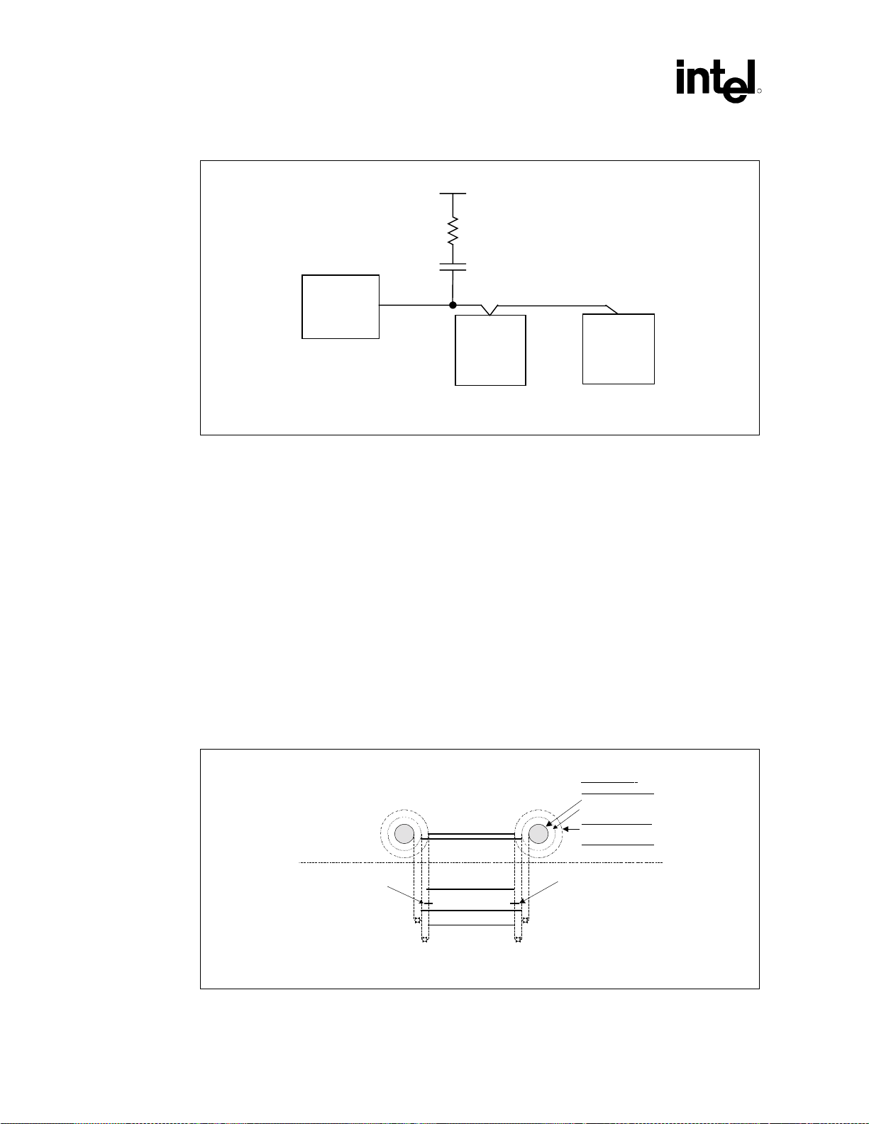
System Bus Routing
Figure 40. Wired OR Topology for Dual Processor Based Systems
VCC_CPU
40 Ω
50 pF
R
Chipset
L1
Proc. 1
L0
Proc. 0
Wire_OR_DP
Design Considerations
Intel has found that the following recommendations aid in the routing of a processor platform. This
is a baseline configuration only. Modify this baseline as needed while adhering to the preceding
design recommendations.
• Trace width = 5.0 mil
• Trace to trace spacing = 15 mil (except in component breakout where spacing is constrained)
• 10 mil vias with a 35 mil pad
• ½ oz copper on signal layers, 1 oz on planes for power delivery
Using the recommendations for via size shown in Figure 41 allows two traces to be routed between
vias, and the traces to overlap the reference plane by no more than 50%. The overlap should occur
only for a short distance.
Figure 41. Via Dimensions and Routing Path
Assumptions:
Inner signal layers:
25 mil hole pad
5 mil clearance
Inner plane layers:
40 mil antipad
Outer plane layers:
38 mil surface anti-pad
Signal Trace
Via_Dimensions_860
Top View
Cross-sectional
View
82 Intel
10 mil power plane
15 mil routing path
Signal Trace
®
Xeon™ Processor and Intel® 860 Chipset Platform Design Guide
10 mil power plane
15 mil routing path
10 mil power plane
5 m ils5 m ils
2.5 mils2.5 mils

System Bus Routing
R
5.4.2 Routing Guidelines for Asynchronous GTL+ and Other System Bus Signals
This section describes layout recommendations for signals not covered in the previous section.
Table 15 describes the signals covered in this section.
Table 15. Asynchronous GTL+ and Miscellaneous Signals
Signal Name Type Processor
A20M# Async GTL+ I 2 ICH2 Processor
BINIT# AGTL+ I/O Refer to
BR[3:1]# AGTL+ I 5 Processor Processor
BR0# AGTL+ I/O 5 Processor/
COMP[1:0] Analog I 6 Pull-down Processor
FERR# Async GTL+ O 1 Processor ICH2
IERR# Async GTL+ O 1 Processor External logic
IGNNE# Async GTL+ I 2 ICH2 Processor
INIT# Async GTL+ I 2 ICH2 Processor
LINT[1:0] Async GTL+ I 2 ICH2 Processor
ODTEN other I 7 Pull-up / pull-
PROCHOT# Async GTL+ O 1 Processor External logic
PWRGOOD Async GTL+ I 2 External logic Processor
RESET# Common
Clock
SLP# Async GTL+ I 2 ICH2 Processor
SM_ALERT# SMBUS
(3.3 V)
SM_CLK SMBUS
(3.3 V)
SM_DAT SMBUS
(3.3 V)
SM_EP_A[2:0] SMBUS
(3.3 V)
SM_TS_A[1:0] SMBUS
(3.3 V)
SM_WP SMBUS
(3.3 V)
I/O Type
I See note 2 MCH Processor
I/O 4 Processor/
I 4 Processor/
I 4 Processor/
I 4 Pull-up / pull-
I 4 Pull-up / pull-
I 4 Pull-up / pull-
Topology
Number
Section
5.4.1.4
Driven by Received by
Processor Processor
MCH
down
ICH2
ICH2
ICH2
down
down
down or
external logic
Processor/
MCH
Processor
ICH2
Processor/
ICH2
Processor/
ICH2
Processor
Processor
Processor
®
Xeon™ Processor and Intel® 860 Chipset Platform Design Guide 83
Intel
System Bus Routing
Signal Name Type Processor
SMI# Async GTL+ I 2 ICH2 Processor
STPCLK# Async GTL+ I 2 ICH2 Processor
TAP signals TAP See Section 16
THERMTRIP# Async GTL+ O Refer to
VCCA Power I See Section 12.17.3
VCCIOPLL Power I See Section 12.17.3
VCCSENSE Other O See Section 12.12
VID[4:0] Other O 3 Processor Voltage
GTLREF Power I See Section 12.17.2
VSSA Power I See Section 12.17.3
VSSSENSE Other O See Section 12.12
I/O Type
Topology
Number
Section
5.4.2.1
R
Driven by Received by
Processor External logic
regulator
NOTES:
1. All signals must meet the AC and DC specifications listed in the Intel® Xeon™ Processor at 1.40 GHz,
1.50 GHz, 1.7 GHz and 2 GHz Datasheet.
2. The Reset# signal should be terminated to the processor VCC_CPU voltage on both ends of the
transmission line similar to the system bus. The Intel Xeon processor and Intel Xeon processor with 512
KB L2 cache do not provide on-die termination for the Reset# signal and hence the platform must
provide the termination. Refer to the ITP700 Debug Port Design Guide for implementation details
affecting the debug port design.
5.4.2.1 Topology 1: Asynchronous GTL+ Signals Driven by the Processor
These signals (FERR#, PROCHOT#, THERMTRIP#, and IERR#) should adhere to the following
routing and layout recommendations. Figure 42 illustrates the recommended topology. When
routing to middle agents connect in true daisy chain topology. Do not create a stub to connect to
the socket pins. Note that FERR# is the only signal in this group that connects between the
processor(s) and the ICH2. PROCHOT#, THERMTRIP# and IERR# are connected to other
motherboard logic.
Because of excessive undershoot observed at the processors, use dual termination on all four
signals for dual processor configurations. Each processor’s signal can be routed to it’s own
receiver, or the signals can be wire-OR’d together. Each signal must be terminated if routed
separately, but the signal can be terminated at the receiver end only. Figure 42 shows the
recommended topology.
Trace Zo Trace Spacing L1 L2 L3 Rpu
50 Ω 10 mil 4–6 inches 1–12 inches 3 inches max 56 Ω ± 5%
®
84 Intel
Xeon™ Processor and Intel® 860 Chipset Platform Design Guide
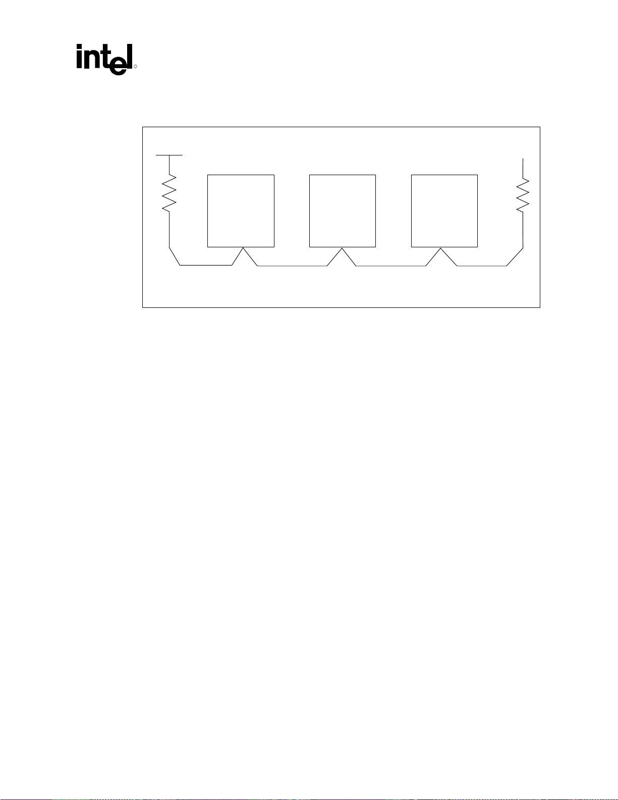
System Bus Routing
R
Figure 42. Topology 1 for DP Configuration
Vcc_CPU
Vcc_CPU
PROC 0 PROC 1
L3
L1 L2 L3
ICH2
Topol_1_DP_860
RPU RPU
To help protect the processor from damage in over-temperature situations, motherboard logic must
ensure that power to the processor core is removed within 0.5 seconds of the assertion of
THERMTRIP#. If power is applied to a processor when no thermal solution is attached, normal
leakage currents will cause the die temperature to rapidly rise to levels at which permanent silicon
damage is possible. This high temperature will cause THERMTRIP# to go active. For details
regarding the THERMTRIP# specification, refer to the processor datasheets referenced in Section
1.1.
Each processor’s THERMTRIP# signal can be routed to its own receiver, or they can be wireOR’d together. If routed separately, each signal should be terminated at the receiver end only
instead of using dual termination. Because this platform utilizes a shared VCC_CPU power plane,
all power supply sources to all processors must be disabled when any installed processor asserts
THERMTRIP#. Figure 43 shows a recommended circuit for disabling power to the processor,
along with related customer reference board logic that interfaces with this THERMTRIP#
shutdown circuit. The 74AHC74 flip-flop latches the THERMTRIP# signal HIGH after a
PWRGOOD assertion, and LOW after a THERMTRIP# assertion. The output of this latch is then
used by the system logic that controls the enable and disable of the processors’ VRD supply. Refer
to the Customer Reference Board Schematics in Appendix A for complete details.
®
Xeon™ Processor and Intel® 860 Chipset Platform Design Guide 85
Intel

System Bus Routing
Figure 43. Recommended THERMTRIP# Circuit
R
12V
3V STANDBY
VCC_CPU
THERMTRIP#
1 KΩ
SKTOCC_1_L
VID_MATCH
3.3 V
62 Ω
0.1 uf
U4G1
9
10
3904
1 kΩ
8
SKTOCC_1
12
13
U4G1
3.3 κΩ
1 kΩ
10 kΩ
3904
U4G1 U4G1
1
2
11
74AHC74
VCC=3V STANDBY
3
SET
D
CLR
4
5
Q
Q
100 Ω
6
VRM_OUTEN
1 kΩ
THERM_EN
5 V
5
Q4G1
3
4
VRM_OUTEN_L
6
12
Q4G1
THERMTRIP#_Ckt
®
86 Intel
Xeon™ Processor and Intel® 860 Chipset Platform Design Guide
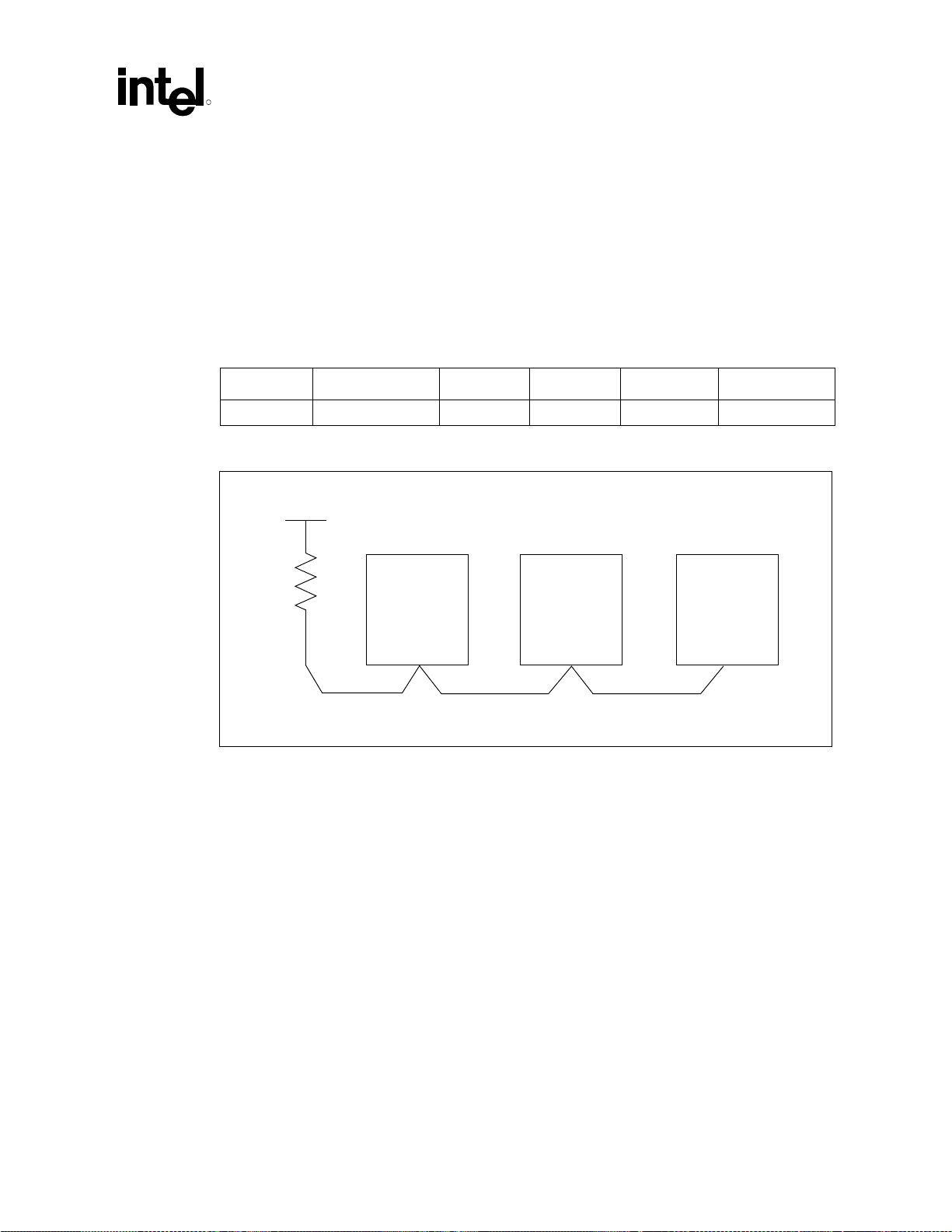
System Bus Routing
R
5.4.2.2 Topology 2: Asynchronous GTL+ Signals Driven by the Chipset
These signals (A20M#, IGNNE#, INIT#, LINT[1:0], PWRGOOD, SLP#, SMI#, and STPCLK#)
should adhere to the following routing and layout recommendations. Figure 44 illustrates the
recommended topology. When routing to middle agents, connect in true daisy chain topology. Do
not create a stub to connect to the socket pins.
It may be desirable to isolate PWRGOOD for each voltage regulation module (VRM) and
processor pair to allow recognition of individual VRM failures.
Trace Zo Trace Spacing L1 L2 L3 Rpu
50 Ω 10 mil 4–6 inches 1–12 inches 3 inches max 300 Ω ± 5%
Figure 44. Topology 2 for DP Configuration
Vcc_CPU
RPU
PROC 0 PROC 1
L3
5.4.2.3 Topology 3: VID[4:0]
The processor VID[4:0] signals should be routed to the voltage regulator. The voltage regulator
controller should provide internal pull-up resistors for these signals. Refer to voltage regulator
design guidelines referenced in Section 1.1 and the specification of the voltage controller specific
to your design for further details.
Because all installed processors must operate at the same voltage (the power plane is shared
between both CPUs), it is advisable to provide a way to check the VID[4:0] values from both
processors are the same, otherwise power should not be output enabled from the VRMs.
ICH2
L1 L2
®
Xeon™ Processor and Intel® 860 Chipset Platform Design Guide 87
Intel

System Bus Routing
5.4.2.4 Topology 4: SMBus Signals
The SMBus signals provide access to the manageability features on the Intel Xeon processor and
Intel Xeon processor with 512 KB L2 cache. The signaling protocol adheres to the specification of
the System Management Bus. Refer to the processor datasheet for details on the processor
implementation and addressing scheme.
The SM_ALERT#, SM_CLK, and SM_DAT signals should be connected to an SMBus controller
in adherence to the System Management Bus Specification, rev2.0. These signals can be connected
to other processors on the same SMBus. Refer to the SMBus and I
for additional design information.
The SM_EP_A[2:0] signals set the SMBus address for the memory device on the processor. These
signals must be set at power on with a unique address per bus. They have an internal 10 k
down. To pull a signal to a logic high level, connect it to a 100
The SM_TS_A[1:0] signals set the SMBus address for the thermal device on the processor. These
signals must be set at power on with a unique address per bus. The SM_TS_A[1:0] can be set to a
logic high, a logic low, or a high impedance state giving nine possible combinations of addresses.
The SM_TS_A[1:0] signals do not have internal pull-downs and must therefore be pulled to VSS
or SM_VCC with a 1 k
Ω or smaller resistor. Leaving the pins floating achieves a high-Z state.
2
C Bus Design application note
Ω pull-
Ω resistor tied to SM_VCC.
R
The SM_WP signal is a write protect signal for the memory device. Pulling this signal to
SM_VCC enables write protection. SM_WP has an internal 10 k
Ω pull-down.
5.4.2.4.1 Considerations for Implementing Manageability Features of the Processor
The Intel Xeon processor and Intel Xeon processor with 512 KB L2 cache include three features
that provide manageability needs beyond the processor core, an on-board thermal sensor, a
Processor Information ROM (PIROM), and an OEM Scratch ROM. These features are accessible
via the System Management Bus (SMBus) interface pins provided by the processor. The SMBus
thermal sensor can be utilized to analyze long-term temperature trends of the processor. The
PIROM contains 128 bytes of information regarding the features and configuration of the
processor. The OEM Scratch ROM provides 128 bytes of space for data to be supplied by the
OEM. Together, these features can be utilized to enhance system manageability, such as
implementing portions of the Intelligent Platform Management Interface (IPMI) Specification.
General Design Considerations
Utilizing the SMBus devices of the processor is not required. While the Intel Xeon processor
utilizes SM_VCC only for the SMBus devices, the Intel Xeon processor with 512 KB L2 cache
requires a valid 3.3V source to SM_VCC because the VID[4:0] pins are driven by logic that is
powered by the SM_VCC supply. Therefore, the SM_VCC supply must be valid before the VRM
supplying VCC_CPU to the processor is enabled. Refer to the Intel® Xeon™ Processor with 512
KB L2 Cache Compatibility Guidelines fo r Intel® Xeon™ Processor-Based Platforms and Intel®
Xeon™ Processor with 512 KB L2 Cache at 1.8 GHz, 2 GHz and 2.2 GHz Datasheet for
implementation details regarding VID and SM_VCC. When configuring the address space of the
SMBus devices, Intel recommends using 1 kΩ pull-up or pull-down resistors.
®
88 Intel
Xeon™ Processor and Intel® 860 Chipset Platform Design Guide

System Bus Routing
R
SMBus Thermal Sensor Design Considerations
The SMBus thermal sensor is configured for its SMBus address space through the processor input
signals SM_TS_A[1:0]. The thermal sensor supports nine unique addresses. This is accomplished
by using three states of decode of the address pins: high, low, and high-Z. With no motherboard
supplied pull up or pull down resistors, the address pins are configured for the high-Z state for
address space determination.
For systems with more than nine thermal sensors utilizing the same address space that exceeds
nine devices, the SMBus will need segmentation to avoid address conflicts. In addition, there may
be cases where segmentation is required due to power availability in various zones of the design.
For example, if some portions of the system can be powered off, it may not be necessary/desired to
monitor thermal activity in that zone and thus power can be removed from the sensors as well.
Segmentation of the SMBus would be necessary so that powered and unpowered devices do not
occupy the same segment.
PIROM and OEM Scratch ROM Design Considerations
The PIROM and OEM Scratch ROM are both contained in the same EEPROM device, and as
such are configured for their address space through a common set of address pins. Processor input
signals SM_EP_A[2:0] configure the address space on the SMBus. Each of these inputs includes a
10 kΩ pull down on the processor interposer. There are eight address options for the ROMs and
these addresses are the same as those found in memory Serial Presence Detect (SPD) devices.
Thus, when implementing the PIROM and Scratch ROM, segmentation of the Smbus is necessary
if there are more than eight SPD and PIROM/Scratch ROM devices in the system.
The PIROM is always write protected. The OEM Scratch ROM space is write protected via the
SM_WP input signal. The processor provides a 10 kΩ pull down resistor on this signal. The
platform may drive this signal with logic or use a pull up of 1 kΩ to enable the write protection of
the Scratch ROM. As with the other SMBus signals, the SM_WP input is 3.3 V compatible.
®
Xeon™ Processor and Intel® 860 Chipset Platform Design Guide 89
Intel

System Bus Routing
5.4.2.5 Topology 5: BR[3:0]# Signals
Because the processor does not include on-die termination for the BR[3:0]# signals, it is necessary
to terminate the signals using discrete components on the motherboard. Connect the BR[1:0]#
signals, as in the past, by “swizzling” the lines between the processors as shown in Figure 45.
Agent-to-agent signal length for the processors should be 4.5 inches. The total bus length can be
no longer than 20.2 inches. Agent-to-agent lengths on BR[1:0]# should be matched within 0.5
inches. For other routing guidelines such as trace spacing and layer referencing, follow the
guidelines for common clock signals in Figure 45. Either terminate BR[3:2]# individually at each
processor, or connect the signals between processors and terminate at one end. Terminate to
VCC_CPU.
Trace
Zo
L1
Agent -
to-agent
L2 (BR0#)
Agent to
Chipset
Agent to Rpu
L3
stub
RT R
PU
R
50 Ω 3.0 to
10.1
inches
Up to 15.7
inches
Up to 1 inch 41Ω ± 5% 41 Ω ± 5%
Figure 45. BR[3:0]# Connection for DP Configuration
Vcc_CPU Vcc_CPU
MCH
L2
R
PU
R
T
Processor 1 Processor 0
BR0# BR1# BR2# BR3#
5.4.2.6 Topology 6: COMP[1:0] Signals
R
T
BR0# BR1# BR2# BR3#
L1
R
L3
BR_DP_Conn
T
Terminate the COMP[1:0] pins to ground through a 43.2 Ω ± 1% resistor. Do not wire the COMP
pins together—connect each pin to its own termination resistor.
®
90 Intel
Xeon™ Processor and Intel® 860 Chipset Platform Design Guide

System Bus Routing
R
5.4.2.7 Topology 7: ODTEN Signal
The end processor in a dual-processor system must have its on-die termination enabled. The
middle agent must disable the on-die termination. To enable, pull the ODTEN pin to a high state
by terminating it to VCC_CPU through a resistor. To disable, pull the ODTEN pin to a low state
by terminating it to ground through a resistor. There are two options for choosing the pull-up and
pull-down resistor values. While both options are suitable for this platform, Option 1 is preferred
over Option 2. The two available options are:
• Option 1 (preferred): Enable ODT (on-die termination) on Processor 0 (end processor) by
pulling up to VCC_CPU with a resistor that matches the motherboard trace impedance within ±
20%. Disable ODT on Processor 1 by pulling down to VSS with a resistor that matches the
motherboard trace impedance within ± 20%. For example, since the recommended nominal
trace impedance is 50 Ω, resistor values within the range of 50 Ω ± 20% should be used for the
pull-up and pull-down.
• Option 2: Enable ODT on Processor 0 (end processor) by pulling up to VCC_CPU with a 1 kΩ
resistor. Disable ODT on Processor 1 by pulling down to VSS with a 1 kΩ resistor.
5.4.2.8 Topology 8: TESTHI[6:0] Signals
For each processor, all TESTHI[6:0] pins must be connected to VCC_CPU via pull-up resistors.
TESTHI[3:0] and TESTHI[6:5] may all be tied together at each processor and pulled up to
VCC_CPU with a single resistor, if desired. However, boundary scan testing will not be functional
if any TESTHI pins are connected together. TESTHI4 must always be pulled up independently
from the other TESTHI pins regardless of the usage of boundary scan. The TESTHI[6:0] signal
group must not be connected between processors. There are four options for choosing the pull-up
and pull-down resistor values. While four options are suitable for this platform, Intel recommends
new designs or designs undergoing design updates follow the trace impedance matching
termination guidelines given in Option 1a or Option 2a. The four available options are:
• Option 1a (preferred): All TESTHI[6:0] pins may be individually pulled-up to VCC_CPU with
resistors. For optimum noise margin, the pull-up resistor value should have a resistance value
within ± 20% of the impedance of the board transmission line traces. Since the recommended
nominal trace impedance is 50 Ω, use resistors that fall within the range of 50 Ω ± 20%.
• Option 1b: All TESTHI[6:0] pins may be individually pulled-up to VCC_CPU with 1 kΩ ± 5%
resistors.
• Option 2a (preferred): TESTHI[3:0] and TESTHI[6:5] may all be tied together and pulled up to
VCC_CPU with a single resistor. For optimum noise margin, the pull-up resistor value should
have a resistance value within ± 20% of the impedance of the board transmission line traces.
Since the recommended nominal trace impedance is 50 Ω, use resistors that fall within the range
of 50 Ω ± 20%. However, utilization of boundary scan test will not be functional if these pins
are connected together. TESTHI4 must always be pulled up independently from the other
TESTHI pins.
• Options 2b: TESTHI[3:0] and TESTHI[6:5] may all be tied together and pulled up to
VCC_CPU with a single 1 kΩ – 4.7 kΩ resistor if desired. However, utilization of boundary
scan test will not be functional if these pins are connected together. TESTHI4 must always be
pulled up independently from the other TESTHI pins.
®
Xeon™ Processor and Intel® 860 Chipset Platform Design Guide 91
Intel

System Bus Routing
j
5.4.2.9 Topology 9: SKTOCC# Signal
The SKTOCC# signal is an output from the processor used as an indication of whether a processor
is installed or not. It will be connected to VSS when a processor is installed in the socket and will
float when there is no processor present. SKTOCC# can be used to disable the VRM output for
unpopulated processor sockets, the power supply output when no processors are installed, system
bus parking in an dual processor system, and other features.
One possible implementation is to disable the bus parking feature of the processor when a second
processor is installed in a dual-processor system. Bus parking allows the current bus owner to
maintain bus ownership even if it currently does not have a pending transaction. If a transaction
becomes pending before that bus owner relinquishes bus ownership, it can drive the transaction
without having to arbitrate for the bus. The parked symmetric agent can then issue transactions 2
clocks sooner than if it had to participate in idle bus arbitration. As a result, enabling bus parking
is strongly recommended for systems that have one processor installed.
For systems with two processors installed, bus parking will increase processor-to-processor bus
ownership exchange by 2 clocks over the ownership-from-idle bus case. Bus parking could reduce
transaction request bandwidth in multi-processor systems in the following cases. As a result, the
ability to disable bus parking is recommend in multi-processor systems. Performance
benchmarking is recommended to determine the optimum setting based on workload and
application.
R
Connect the SKTOCC# of the second processor to the MCH’s BUSPARK enable pin. Refer to the
diagram in the following figure. The pull-up and pull-down resistors and the jumper block shown
in the figure are optional.
Figure 46. SKTOCC# Connection to Chipset BUSPARK Signal
Chipset
BUSPARK SKTOCC#
Note: For debug purposes, utilize a 3-pin
umper block and pull-up/pull-down resistors
to configure buspark, leaving the R3 resistor empty.
V
DDQ
R1
1 kΩ
R2
1 kΩ
R3
1 kΩ
Second Processor
Socket
SKTOCC#_BUSPARK
®
92 Intel
Xeon™ Processor and Intel® 860 Chipset Platform Design Guide

System Bus Routing
µ
R
5.5 MCH System Bus Interface
A voltage divider network should supply host interface reference voltages locally as shown in
Figure 47 and Figure 48, as specified in Table 16.
Figure 47. Voltage Divider Network for Reference Voltage Generation
Vcc
R2
R1
Note the following:
• The MCH must have only one dedicated voltage divider.
• Decouple the voltage divider with a 1 µF capacitor.
• Keep the voltage divider within 1.5 inches of the MCH V
Figure 48. Pull-Down Circuit
L1 = 1.5" max
F
1
R
Tline
220 pF
socket pin
ball.
REF
1
V
SS
®
Xeon™ Processor and Intel® 860 Chipset Platform Design Guide 93
Intel

System Bus Routing
Table 16. Reference Voltage Network Values
Signal R1 R2 Tolerance Figure Notes
HDVREF[3:0] 100 Ω 50 Ω ± 1% Figure 47 1,2
HAVREF[1:0] 100 Ω 50 Ω ± 1% Figure 47 1,2
CCVREF 100 Ω 50 Ω ± 1% Figure 47 1,2
HRCOMP[1:0] 20.75 Ω — ± 1% Figure 48 3
HSWNG[1:0] 150 Ω 301 Ω ± 1% Figure 47 4
NOTES:
1. 2/3 Vtt Resistor Network.
2. Single voltage divider for these signals.
3. Independent of board impedance.
4. 1/3 Vtt Resistor Network.
5.5.1 MCH System Bus I/O Decoupling Recommendations
R
The primary objective of the decoupling recommendations for the chipset is to provide clean
power delivery to the system bus I/O buffers. The split plane nature of chipsets creates power
delivery concern.
The secondary objective of decoupling at the chipset is to minimize the impact of return path
discontinuities that may occur between the chipset package and the motherboard. A return path
discontinuity occurs in systems whose signals reference either power or ground, but not both (the
chipset uses symmetric stripline interconnects that reference the signal to both Vcc and VSS).
Systems that have this type of discontinuity (such as the recommended dual processor stack-up)
should use the larger number of decoupling capacitors listed in the following guidelines for the
chipset.
The following are decoupling recommendations for the MCH (see Figure 49):
• 4 minimum, 5 preferred 0.1 µF capacitors with 0603 packages distributed evenly over the
system bus data lines
• 2 minimum, 3 preferred 0.1 µF capacitors with 0603 packages distributed evenly over the
system bus address and control lines
• All capacitors placed as close as possible to the MCH package (within 150 mils).
®
94 Intel
Xeon™ Processor and Intel® 860 Chipset Platform Design Guide

System Bus Routing
R
Figure 49. I/O Decoupling Guidelines for the MCH
Address and
Control Field
2-3 0.1 µF with 603 body
over the address and
control signals and as
close to the chipset
package as possible.
Example
Chipset
Package
Data Field
4-5 0.1 µF with 603 body
over the data signals and as
close to the chipset package
as possible.
Chipset_Decouple_Exa
®
Xeon™ Processor and Intel® 860 Chipset Platform Design Guide 95
Intel

System Bus Routing
This page is intentionally left blank.
R
®
96 Intel
Xeon™ Processor and Intel® 860 Chipset Platform Design Guide

Memory Interface Routing
R
6 Memory Interface Routing
6.1 Rambus* Channel Overview
The Rambus Channel is a multi-symbol interconnect. Because of the length of the interconnect and
the frequency of operation, this bus is designed to allow multiple command and data packets to be
present on a signal wire at any given instant. For example, the driving device can send the next
data out before the previous data has left the bus.
The nature of the multi-symbol interconnect forces many requirements on the bus design and
topology. First and foremost, a drastic reduction in reflected voltage levels is necessary. The
interconnect transmission lines must be terminated at their characteristic impedance; otherwise the
reflected voltage resulting from a mismatch in impedance will degrade signal quality. These
reflections reduce noise, timing margins and the maximum operating frequency of the bus. Second,
coupled noise can greatly affect the performance of high-speed interfaces. Just as in source
synchronous designs, odd and even mode propagation velocity change can create skew between
the clock and data or command lines which reduces the maximum operating frequency of the bus.
Efforts must be made to significantly decrease crosstalk, as well as the other sources of skew.
To achieve these bus requirements, the Rambus Channel is designed to operate as a transmission
line. All components, including the individual Direct RDRAM devices, are incorporated into the
design to create a uniform bus structure that can support up to 33 devices (including the MCH)
running at 800 MegaTransfers/second (MT/s).
The following sections describe the design guidelines that help ensure a robust Rambus Channel
design.
For more information regarding Direct RDRAM device technology, refer to
http://www.rambus.com/developer/quickfind_documents.html
The Intel 860 chipset supports the following types of memory configurations on its Direct
RDRAM devices interface:
• The Memory Expansion Card (MEC).
• Direct RDRAM devices on the system board.
.
®
Xeon™ Processor and Intel® 860 Chipset Platform Design Guide 97
Intel

Memory Interface Routing
6.2 Memory Design with MEC/MECC (Inner Layer Routing)
The Memory Expansion Card (MEC) concept is intended to provide flexibility and scalability of
memory to an Intel 860 chipset-based workstation platform. The Intel 860 chipset supports both
RIMM modules down and MECC configurations. For routing guidelines for the Memory
Expansion Card (MEC), refer to the Intel
Guide.
The MCH-to-MECC routing guidelines are based on the usage of a Memory Expansion Card
Connector (MECC) that meets the RIMM connector specification electrical characteristics.
Figure 50. Rambus* Channel Signal Groups
®
860 Chipset Memory Expansion Card (MEC) Design
R
M
82840
MCH
3.0" < a < 4.5"
mch_mecc_lay_860
All Direct RDRAM device signals lengths between the MCH and the MECC should be between
3.0 inches (min) and 4.5 inches (max). Although channels A and B are not required to match one
another, the difference between channels should be minimized and must meet MCH levelization
requirements.
Refer to the Intel
and other signal routing guidelines to expansion devices (MRH-R).
To maintain 28 Ω trace impedance, the RSL signals must be 18 mil wide. To control crosstalk and
odd/even mode velocity deltas, there must be a 10 mil ground isolation trace between adjacent
RSL signals. The 10 mil ground isolation traces must be connected to ground with a via every 1
inch. A 6 mil gap is required between the RSL signals and ground isolation traces. To ensure
uniform traces, the trace width variation must be uniform on all RSL signals at every neck down.
The RSL signals within each channel must be length matched to ± 10 mils in the line section
between the MCH and first device (MRH-R) on the MEC using trace length matching methods.
®
860 Chipset Memory Expansion Card (MEC) Design Guide for complete RSL
E
C
C
Also, all RSL signals must have the same number of vias. It may be necessary to place additional
vias (dummy vias) on RSL signals to meet the via-loading (equal number of vias) requirement,
even if vias are not needed. Refer to the Intel
and other signal routing guidelines to expansion devices (MRH-R).
®
98 Intel
Xeon™ Processor and Intel® 860 Chipset Platform Design Guide
®
860 Chipset MEC Design Guide for complete RSL
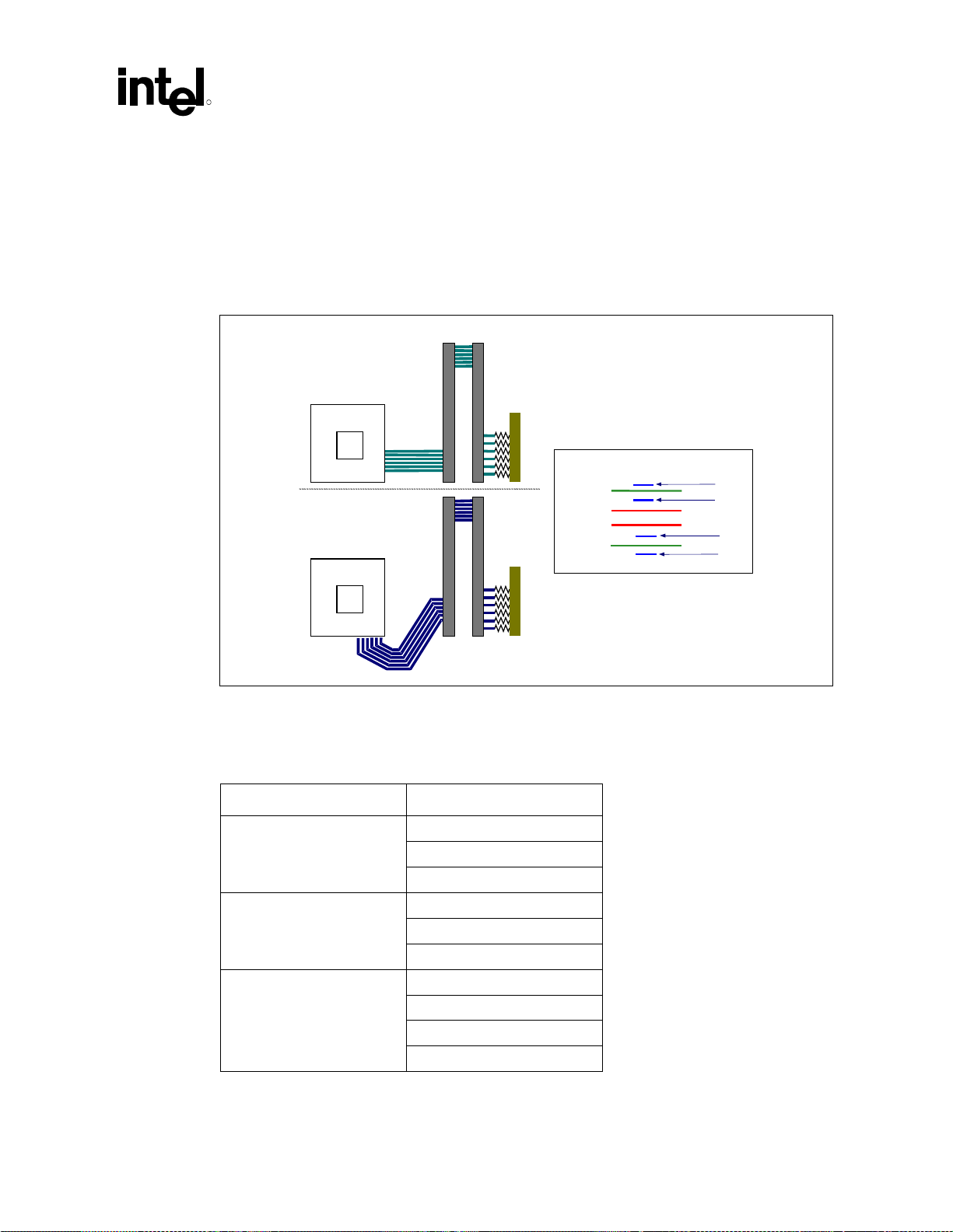
Memory Interface Routing
A
R
6.3 Rambus* Channel Routing Guidelines
The MCH has two Rambus Channels. The following layout guidelines are applicable for each
channel. Because of routing and timing margin, one channel should be routed entirely microstrip
(outer layers) or stripline (inner layers). Figure 51 illustrates an example routing topology for the
MCH.
Figure 51. Intel
The signals on the Rambus Channel are broken into three groups: Rambus Signaling Level (RSL)
signals, CMOS signals, and clocking signals. The signal groups are described in Table 17.
®
860 Chipset MCH Rambus* Channel Routing Example
MCH
MCH
RAC*
RIMM* Connector
RIMM Connector
RAC*
V
T
RIMM Connector
E
R
M
Vss plane
Vcc plane
RIMM Connector
Vcc plane
Vss plane
V
T
E
R
M
Layer 0
Layer 2
Layer 5
Layer 7
Board Stack-Up
8 Layers
Layer 1
Layer 3
Layer 4
Layer 6
Signal
Signal
Signal
Signal
Table 17. Rambus* Channel Signal Groups
Group Signal
RSL Signals DQA[8:0]
DQB[8:0]
RQ[7:0]
*(1)
(1)
CMOS Signals CMD
SCK
SIO
Clocking Signals CTM
CTM#
CFM
CFM#
NOTE: These are high-speed CMOS signals
®
Xeon™ Processor and Intel® 860 Chipset Platform Design Guide 99
Intel

Memory Interface Routing
6.3.1 Rambus* Signaling Level (RSL) Signals
The Rambus Channel RSL signals are high-speed signals that transmit data between the MCH and
RDRAM component at a maximum speed of 800 MHz. These signals start at the MCH, enter the
first RIMM connector on either side, propagate through the RIMM connector, and then exit on the
opposite side. The RSL signals continue through the second RIMM connector until they are
terminated at Vterm. All unpopulated RIMM connector slots must have continuity modules in
place to ensure that signals propagate to the termination at the end of the Rambus Channel.
The perfect matching of transmission line impedance and uniform trace length are essential for the
Direct RDRAM device interface to work properly. Maintaining 28 Ω ± 10% loaded impedance for
every RSL signal requires some changes to the standard trace width and board prepreg thickness.
Typically, 28 Ω nominal impedance with 7 mil prepreg requires 28 mil wide traces. 28 mils wide
traces are too wide to break out of the rows of RSL signals on the MCH. To reduce the trace
width, a thinner prepreg is required. For example, a prepreg thickness of 4.0 mils to 4.5 mils
allows 18 mil wide traces to meet the 28 Ω ± 10% nominal impedance requirement.
The following figure and table describe the Rambus Channel topology for a 28 Ω channel.
R
Figure 52. Example Rambus* Channel Routing
MCH
A
MCH to
First RI MM* conn.
B
RIMM conn. to
RIMM conn.
RIMM con nector t o
Termination
Term
C
Note: This diagram only illustrates the routing of one Rambus Channel. However, the example routing
shown can be applied to both channels.
Table 18. Rambus* Channel RSL Signal Lengths for RIMM* Connectors on Motherboard
Reference Section Trace Description Trace Length
A MCH to first RIMM connector for Rambus*
Channel A or first RIMM for Rambus
Channel B
B RIMM connector to RIMM connector for
the same channel
C RIMM connector to Termination 0 inch to 2 inches
1 inch to 6 inches
0.4 inch to 1 inch
(1)
NOTES:
1. Place termination resistors between RIMM connectors of the same channel, when possible, to reduce
the trace length.
®
100 Intel
Xeon™ Processor and Intel® 860 Chipset Platform Design Guide
 Loading...