

Intel 82815E (GMCH) Intel Celeron/Intel Pentium III Processor - Low Power/Ultra Low Power (BGA2) and Intel 815E Chipset Design Guide

R
Intel®Celeron®/Intel®Pentium®III
Processor - Low Power/Ultra
®
Low Power (BGA2) and Intel
815E Chipset
Design Guide
May 2002
Document Number: 273630-001

Introduction
R
Information in this Information in this document is provided in connection with I ntel®products.
No license, express or implied, by estoppel orotherwise, to anyintellectual property rights is granted bythis document. Except as provided in I ntel’s
Terms and Conditions of Sale forsuch products, Intel assumes no liabilitywhatsoever,and Inteldisclaims anyexpress or impliedwarranty,relating
to sale and/or use of Intel products including liability orwarrantiesrelating to fitnessfor aparticular purpose, merchantability, orinfringement of any
patent, copyright or other intellectual property right. Intel products are not intended for use in medical, life saving,or life sustaining applications.
Intel maymake changes tospecifications and product descriptions at any time, without notice.
Designers must notrelyon the absence or characteristics of anyfeatures or instructions marked "reserved"or "undefined." Intel reserves these for
future definition and shall haveno responsibilitywhatsoeverfor conflicts or incompatibilities arising from futurechanges to them.
The Intel® <product name> maycontain design defects or errors known as errata which may cause the product to deviate from published
specifications. Current characterized errata are available on request.
Contact your local Intel sales office or yourdistributor to obtain thelatest specifications and before placing your product order.
Copies of documents which have an ordering number andare referenced in this document, or other Intel literature, may be obtained from:
Intel Corporation
www.intel.com
or call 1-800-548-4725
Copyright © 200x ,Intel Corporation
AlertVIEW, i960, AnyPoint, AppChoice, BoardWatch, BunnyPeople, CablePort, Celeron, Chips, Commerce Cart, CT Connect, CT Media, Dialogic,
DM3, EtherExpress, ETOX, FlashFile, GatherRound, i386, i486, iCat, iCOMP, Insight960, InstantIP,Intel, Intel logo, Intel386, Intel486, Intel740,
IntelDX2, IntelDX4,IntelSX2, Intel ChatPad, Intel Create&Share, Intel Dot.Station, Intel GigaBlade, Intel InBusiness, Intel Inside, Intel Inside logo,
Intel NetBurst, Intel NetStructure, Intel Play, Intel Playlogo, Intel Pocket Concert, IntelSingleDriver, Intel SpeedStep, Intel StrataFlash, Intel
TeamStation, Intel WebOutfitter, Intel Xeon, Intel XScale, Itanium, JobAnalyst, LANDesk, LanRover, MCS, MMX,MMX logo, NetPort,
NetportExpress, Optimizer logo, OverDrive, Paragon, PCDads, PC Parents, Pentium, Pentium IIXeon, Pentium IIIXeon, Performance atYour
Command, ProShare, RemoteExpress, Screamline, Shiva,SmartDie, Solutions960, Sound Mark, StorageExpress, The Computer Inside, The
JourneyInside,T his Way In, TokenExpress, Trillium,Vivonic, and VTune are trademarks or registered trademarks of Intel Corporation or its
subsidiaries in the United States andother countries.
*Other names and brands maybe claimed as thepropertyof others.
2 Intel®Pentium®III and Intel Celeron®– Low Power/Ultra Low Power / 815E Design Guide

R
Revision History
Rev. No. Description Rev. Date
001 Initial Release May2002
Introduction
Intel®Pentium®III and Intel Celeron®– Low Power/Ultra Low Power / 815E Design Guide 3

Introduction
Table of Contents
1 Introduction ....................................................................................................................5
1.1 Audience............................................................................................................ 5
1.2 Notation and Terminology.................................................................................. 6
1.3 Reference Documents........................................................................................8
2 General Design Considerations......................................................................................9
2.1 Nominal Board Stack-up....................................................................................9
3 Processor Host Bus Design.......................................................................................... 10
3.1 Initial Timing Analysis...................................................................................... 10
3.2 General Topology and Layout Guidelines......................................................... 13
3.3 Simulation Methodology................................................................................... 13
3.3.1 Pre-Layout Simulation....................................................................... 13
3.3.2 Post-Layout Simulation..................................................................... 14
3.4 Layout Rules for GTL+ Signals ........................................................................ 14
3.5 Layout Rules for Non-GTL+ (CMOS) Signals...................................................16
3.5.1 Additional Routing and Placement Considerations ............................16
3.6 Undershoot/Overshoot Requirements............................................................... 16
3.7 Processor Reset Requirements........................................................................ 17
3.8 Debug Port Routing Guidelines........................................................................ 18
3.9 PLL Filter Recommendations........................................................................... 19
3.9.1 Topology...........................................................................................19
3.9.2 Filter Specification ............................................................................ 21
3.10 Decoupling Guidelines for BGA2-based Processors......................................... 23
3.11 Catastrophic Thermal Protection......................................................................23
R
4 Clocking .......................................................................................................................24
4.1 General Clocking Considerations ..................................................................... 24
4.2 Single-Ended Host Bus Clocking Routing......................................................... 24
4.2.1 CLKREF Filter Implementation.......................................................... 26
4.2.2 Single-Ended Clocking BSEL[1:0] Implementation ............................ 27
4.2.3 Clock Driver Decoupling and Power Delivery .................................... 27
5 Processor Host Bus Design Checklist........................................................................... 28
5.1 Introduction......................................................................................................28
5.2 GTL+ Checklist................................................................................................ 28
5.2.1 CMOS (Non-GTL+) Checklist............................................................ 29
5.3 TAP Checklist..................................................................................................29
5.3.1 Miscellaneous Checklist....................................................................30
6 Reference Schematic................................................................................................... 31
4 Intel®Pentium®III and Intel Celeron®– Low Power/Ultra Low Power / 815E Design Guide

R
1 Introduction
This document provides design guidelines for developing systems based on the Intel® Celeron®
Processor – Low Power or Ultra Low Power or Intel® Pentium® III - Low Power in a BGA2
packageandtheIntel
presented. Likely design errors have been listed here in a checklist format. These are
recommendations only.
These design guidelines and recommendations have been simulated and validated and strongly
recommended to meet the timing and signal quality specifications. It is recommended that
simulations be performed to meet design-specific requirements.
Note: The system bus speed supported by the design is based on the capabilities ofthe processor,
chipset, and clock driver.
® 815E chipset. Special design recommendations and concerns are
Introduction
1.1 Audience
This document is intended to be used by Intel® Celeron® or Intel® Pentium® III –
LP/ULP/815E system developers.
Intel®Pentium®III and Intel Celeron®– Low Power/Ultra Low Power / 815E Design Guide 5

Introduction
1.2 Notation and Terminology
This section describes someof the terms used in this document.
Term Description
AGP AcceleratedGraphics Port
GTL+ Refers to processor bus signals that are implemented open drain GTL+ interface
signal.
Bus Agent A componentor group of compo nents that, whencombined, representasingle load on
the AGTL bus.
Crosstalk The reception o na victim network of asignal impose dby aggressor network(s) through
inductive andcapacitivecoupling betweenthenetworks.
• Backward Crosstalk–coupling that creates asignal in avictim network that travels in
the opposite direction as theaggressor signal.
• Forward Crosstalk–coupling that creates a signal in a victim network that travels in
the same direction as the aggressor signal.
• Even ModeCrosstalk–coupling from single or multipleaggressors when all the
aggressors switch in thesa m edirection that thevictim is switching.
• Odd Mode Crosstalk–coupling from single or multipleaggressors when all the
aggressorsswitchin theoppositedirection thatthe victim isswitching.
R
GMCH Graphics and MemoryController Hub. A component o f theIntel®815chipsetplatform
for use withIntel
Power
ICH2 Intel®82801BA I/O Controller Hub component.
ISI Inter-symbol interferenceis theeffect of a previo us signal(o rtra nsition)on the
interconnect dela y. For example ,when asignal is transmitted dow na line and the
reflections due tothetransition have not completelydissipated,thefollowing data
transition launched onto thebus is affected. ISI is dependent upon frequency,time
delay of the line, and the reflection coefficient at the driver and receiver. ISI can impact
both timing andsignalintegrity.
Network Length The distance between agent 0 pins and the agent pins at the far end of the bus.
Pad The electrical contact pointof a semiconductor dietothe package substrate. A padis
onlyobservablein simulation.
Pin The contact point of acomponent packageto the traces on asubstrate such as the
motherboard. Signal qualityand timings can be measured at the pin.
Ringback The voltage thata signal rings back to after achiev ingits maximumabsolute value .
Ringback maybedue to reflections, drive roscillations, or other transmission line
phenome na.
Setup Window The time between thebeginning of Setup to Clock (T
clock edge. This windowmay bedifferent for ea ch type of bus agent in the system.
®
Pentium III-Low Power an dIntel®Celeron-Ultra Low Power/Low
) and the arrival of a valid
SU_MIN
6 Intel®Pentium®III and Intel Celeron®– Low Power/Ultra Low Power / 815E Design Guide

Introduction
R
Term Description
SSO Simultaneous Switching Output (SSO) Effects refers to the difference in electrical
timing parameters and degradation in signalquality causedbymultiple signal outputs
simultaneously switching voltage levels (e.g., high-to-low) in the opposite direction from
a single signal (e .g.,low-to-high) or inthesamedirection (e.g., high-to-low). These are
respectivelycalled odd-modeswitching and even-modeswitching. This simultaneous
switching of multiple outputs creates highercurrent swings that ma ycause additional
propagation delay (or “push-out”), or a decrease in propagation delay (or “pull-in”).
These SSO effects may impact the setup and/or hold times and are not always taken
into account bysimulations. Systemtimingbudgets need toinclude ma rginfor SSO
effects.
Stub The branch from the bus trunk terminatingat the pa dof an agent.
SystemBus Thesystembus isthe processorbus.
Trunk The mainconnection, ex cluding inte rconnect branches, from one end agentpad to the
other end agent pad.
Undershoot Minimum voltage observed for a signal to extend below VSSat the device pad.
Victim A network that receives a coupled crosstalk signal from another network is called the
victim network.
In this document, a ‘#’ symbol after a signal name identifies the signal as active low; that is, a
signal that is in the active state, based on the name of the signal, when dr iven to a low level. For
example, when FLUSH# is low, a flush has been requested. When NMI is high, a non-maskable
interrupt has occurred. When a signal name does not imply an active state, a # symbol indicates
that th e signal is inverted. For example, D[3:0] = ‘HLHL’ refers to a hex ‘A’, and D[3:0]# =
‘LHLH’ also refers to a hex ‘A’ (H= High logic level, L= Low logic level).
The term “BGA2-based processor(s)” refers to the Intel® Celeron® processor-Ultra Low Power
and Low Power in a BGA2 package and th e Intel® Pentium® III processor-Low Power in a
BGA2 package.
Intel®Pentium®III and Intel Celeron®– Low Power/Ultra Low Power / 815E Design Guide 7

Introduction
1.3 Reference Documents
The reader of this document needs to be familiar with the material and concepts presented in th e
following documents.
R
Document Document Number /
Intel®815 Chipset Family: 82815 Graphics and Memory Controll erHub (GMCH) for
use with the Universal Socket 370 Datasheet
Intel®82802AB/82802AC Firmware Hub (FWH) Datasheet 290658
Intel®82801BA I/O Controller Hub (ICH2) and Intel®82801BAM I/O Controller Hub
(ICH2-M) Datasheet
Intel®Pentium®IIIProcessor-Low Power Datasheet 273500
Intel®Celeron®Processor-Ultra Low Power/Low Power Datasheet 273509
Intel® 815EM Chipset: 82815EM Graphics and Memory Controller Hub (GMCH2-
M)
Intel® 815EM Chipset Platform Design Guide 298241
Intel® 815E Chipset Platform Design Guide 298234
Intel® 815E Chipset Platform For Use With Universal Socket 370 Design Guide 298350
Accelerated Graphics Port Interface Specification, Revision 2.0
PCI Local Bus Specification, Revision 2.2
AC’97 2.1 Specification http://dev eloper.intel.co
82562EH HomePNA 1 Mb/s Physical Layer Interface Datasheet (Doc # 278313)
82562EH HomePNA 1 Mb/s Physical Layer Interface Brief Datasheet (Doc # 278314)
Communication Network Riser Specification, Revision 1.1 http://dev eloper.intel.co
Universal Serial Bus, Revision1.0 Specification
Location
298351
290687
290689
m/pcsupp/platform/ac97/inde
x.htm.
http://dev eloper.intel.co
m
http://dev eloper.intel.co
m
m/technology /cnr/
8 Intel®Pentium®III and Intel Celeron®– Low Power/Ultra Low Power / 815E Design Guide

General Design Considerations
R
2 General Design Considerations
This section documents the example of a nominal board stack up for BGA2-based processor with
the 815E platform.
Make sure the impedance for all signal layers is 60 Ω±15%. That is, the impedance of the trace
when not subjected to fields created by changing current in neighboring traces. When calculating
flight times, it is important to consider the minimum and maximum impedance of a trace, based
on the switching of neighboring traces. The use of wider spaces between the tr aces can minimize
this trace-to-trace coupling. In addition, th ese wider spaces reduce crosstalk and settling time.
Coupling between two traces is a function of the coupled length, the distance separating th e
traces, the signal edge rate, and the degree of mutual capacitance and inductance. To minimize
the effects of trace-to-trace coupling, follow the routing guidelines documented in this section.
The routing guidelines in this design guide have been created using a PCB stack-up similar to
that in Figure 1. When this stack-up is not used, thorough simulations of every interface must be
completed. Using a thicker dielectric (prepreg) makes routing very difficult or impossible.
2.1 Nominal Board Stack-up
The BGA2-based processor/815E platform requires a board stack-up yielding a target impedance
of 60 Ω ± 15% with a 5 mil nominal trace width. Figure 1 shows an example stack-up achieving
this. It is a 6-layer printed circuit board (PCB) construction using 53%-resin FR4 material.
Figure 1. Board Construction Example for 60 ΩΩΩΩ Nominal Stack-up
Signal/Powerplane layer ½ozCu., 1ozPlating
Prepreg = 3mils
GroundLayer1ozCu.
Core = 6 mils
Signal layer 1 oz Cu.
Prepreg = 34 mils
Signal layer 1 oz Cu.
Core = 6 mils
Ground layer 1 oz Cu.
Prepreg =3 mils
Signal/Powerlayer ½ oz Cu., 1ozPlating
Dieletric Constant for FR4 = 4.2
4 mils tr ace width for outer layers gives a 50 Ω signal impedance.
5 mils tr ace width for inner layers gives a 60 Ω signal impedance
Total thickness:
62 mils
Additional guidelines on board stack-up, placement, and layout include the following.
− The board impedance (Z) is 60 Ω ± 15%.
− The dielectric process variation in the PCB fabrication is minimized.
− The ground plane is not split on the ground plane layer.
− Keep vias for decoupling capacitors as close to the capacitor pads as possible.
Intel®Pentium®III and Intel Celeron®– Low Power/Ultra Low Power / 815E Design Guide 9

Processor Host Bus Design
3 Processor Host Bus Design
This section documents the layout and routing guidelines using the BGA2-based processor with
the Intel® 815E chipset platform. The solution covers system bus speeds of 100 MHz only. The
Ω
processor must also be configured to 56.2
discuss the functional aspect of any bus or the layout guideline for an add-in device.
When the guidelines listed in this document are not followed, it is very important that thorough
signal integrity and timing simulations be completed for each design. Even when the guidelines
are followed, simulate critical signals to ensure proper signal integrity and flight time. As bus
speeds increase, it is imperative that the guidelines documented are followed precisely. Simulate
any deviation from these guidelines.
3.1 Initial Timing Analy s is
To determine the available flight time window, perform an initial timing analysis. Analysis of
setup and hold conditions determine the minimum and maximum flight time bounds for the
system bus. Use the following equations to establish th e system flight time limits.
± 1% on-die termination. The document does not
R
Table 1. System Timing Equations
T
T
flight,min
flight,max
>= T
hold–Tco,min+Tskew
<= T
cycle–Tco,max–Tsu–Tskew–Tjit–Tadj
Table 2. System Timing Terms
Term Description
T
cycle
T
flight,min
T
flight,max
T
co,max
T
co,min
T
su
System cycle time, defined as th e reciprocal of the frequency.
Minimum system flight time.
Maximum system flight time.
Maximum driver delay from input clock to output data.
Minimum driver delay from input clock to output data.
Minimum setup time. Defined as the time for which the input data must be valid
prior to the input clock.
T
hold
Minimum hold time. Defined as the time for which the input data must remain
valid after the input clock.
T
skew
Clock generator skew. Defined as the maximum delay variation between output
clock signals from the system clock generator, the maximum delay variation
between clock signals due to system board variation and chipset loading variation.
T
jit
T
adj
Clock jitter. Defined as maximum edge to edge variation in a given clock signal.
Multi-bit timing adjustment factor. This term accounts for the additional delay
that occurs in the network when multiple data bits switch in the same cycle. The
adjustment factor includes such mechanisms as package and PCB crosstalk, high
inductance current return paths, and simultaneous switching noise.
Equation
10 Intel®Pentium®III and Intel Celeron®– Low Power/Ultra Low Power / 815E Design Guide

Processor Host Bus Design
R
Table 3 lists the GTL+ component timings of the processors and GMCHdefined at the pins for
the Intel® 815E platform.
Note: These timings are for r eference only. Obtain the processor specifications from respective
processor datasheet and chipset values from the appropriate Intel® 815E chipset datasheet.
Table 3. Intel® Celeron® - Ultra Low Power and 82815E GMCH GTL+ Parameters for
Example Calculations
IC Parameters Intel®Celeron®-Ultra
Clock to Output maximum(T
Clock to Output minimum (T
Setup time(T
Holdtime (T
NOTES:
1. All time in nanoseconds
2. Numbers in table are for reference only. These timing parameters are subject to change. Check the
appropriatecomponent documentatio nfor validtimingparamete rvalues.
) 1.20 2.65 1,2
SU_MIN
) 1.20 0.10 1
HOLD
) 3.40 4.10 1,2
CO_MAX
) 0.20 1.05 1,2
CO_MIN
Low Power processor
core at 100 MHz
System Bus
82815E GMCH Notes
Table 4 provides an exampleGTL+ initial maximum flight time and Table 5 is an example
minimum flight time calculation for a 100 MHz, uni-processor system using the Intel®
Celeron® -Ultra Low Power processor/Intel
®
815E chipset system bus. Note that assumed values
for clock skew and clock jitter were used. Clock skew and clock jitter values are dependent on
the clock components and distribution method chosenfor a particular design and must be
budgeted into the initial timing equations as appropriate for each design.
Table4andTable5arederivedassuming:
SKEW = 0.20 ns (Note: Assumes clock driver pin-to-pin skew is reduced to 50 ps by
• CLK
tying two host clock outputs together (“ganging”) at clock driver output pins, and the PCB
clock routing skew is 150 ps. System timing budget must assume 0.175 ns of clock driver
skew and 150 ps PCB clock routing skew if outputs are not tied together and a clock driver
that meets the CK815E Clock Synthesizer/ Driver Specification is being used.)
JITTER = 0.250 ns
• CLK
See the appropriateIntel
®
815E chipset documentation, and CK815E Clock Synthesizer/Driver
Specification for details on clock skew and jitter specifications. Exact details of host clock
routing topology are provided with the platform design guideline.
Table 4. Example T
Driver Receiver Clk Period2TCO_MAX TSU_MIN ClkSKEW ClkJITTER TADJ Recommended
Processor GMCH 10.00 3.40 2.65 0.20 0.25 0.50 3.000
GMCH Processor 10.00 4.10 1.20 0.20 0.25 0.50 3.750
NOTES:
1. All times in nanoseco nds
2. BCLK period = 10.00ns @ 100MHz
FLT_MAX
Calculations For 100 MHz Bus
FLT_MAX
T
Intel®Pentium®III and Intel Celeron®– Low Power/Ultra Low Power / 815E Design Guide 11

Processor Host Bus Design
R
Table 5. Example T
Driver Receiver THOLD ClkSKEW TCO_MIN Recommended
Processor GMCH 0.10 0.20 0.200 0.100
GMCH Processor 1.20 0.20 1.050 0.350
The flight times in Table 4 include margin to account for the following phenomena that Intel
observed when multiple bits are switching simultaneously. These multi-bit effects can adversely
affect the flight time and signal quality and sometimes are not accounted for durin g simulation.
Accordingly, the maximum flight times depend on the baseboard design, an d additional
adjustment factors or margins are recommended.
• SSO push-out or pull-in
• Rising or falling edge rate degradation at the receiver caused by inductance in the
current return path, requiring extrapolation that causes additional delay
• Crosstalk on the PCB and inside the package which can cause variation in the signals
Additional effects exist that may not necessarily be covered by the multi-bit adjustment factor
and need to be budgeted as appropriate to the baseboard design. These effects are included as
in th e examplecalculations in Table 4. Examples include:
T
ADJ
• The effective board propagation constant (SEFF), which is a function of:
FLT_MIN
Calculations (Frequency Independent)
FLT_MIN
T
ε
- Dielectric constant (
)ofthePCBmaterial
r
- Type oftraceconnecting the components (stripline or microstrip)
- Length of the trace an d the load of the components on the trace. Note that the board
propagation constant multiplied by the trace length is a component of the flight time,
but not necessarily equal to the flight time.
12 Intel®Pentium®III and Intel Celeron®– Low Power/Ultra Low Power / 815E Design Guide

Processor Host Bus Design
R
3.2 General Topology and Layout Guidelines
Figure 2. Topology for BGA2 Designs with Single-Ended Termination (SET)
16
GMCH
BGA2-based
Processor
Z
O
Table 6. Trace Guidelines Recommedation
Description Min. Length (inches) Max. Length (inches)
GMCH to BGA2-based processor
trace
NOTES:
1. Reference a ll GTL+ bus signals to the ground pla nefor thee ntireroute.
2. Use an intragroupGTL+ spacing : line width : dielectric thickness ratio of at least 2:1:1 for microstrip
geometry. If
mils spacing, 5 mils trace width, and a 5 mils prepreg between the signal layer and the plane it references
(assuming a 6-layer board design)
3. The recomme nde dtrace widthis 5 mils, but not grea ter than 6 mils.
ε
= 4.5, this limits coupling to3.4%. Fo re xample ,intragro upGTL+ routing could use 10
r
%1560 ±Ω=
1, 2, 3
3.3 Simulation Methodology
3.3.1 Pre-Layout Simulation
Analog simulations are recommended for high-speed system bus designs. Start simulations prior
to layout. Pre-layout simulations provide a detailed picture of the working “solution space” that
meets flight time and signal qualityrequirements. By basing board layout guidelines on the
solution space, the iterations between layout and post-layout simulations can be r educed.
3.50 5.00
Intel recommends running simulations at the device pads for signal quality and at the device pins
for timing analysis. However, simulation results at the device pins may be used later to correlate
simulation performance against actual system measurements.
The BGA2-based processor and 815E I/O buffer models are available from Intel through your
Intel representative.
Intel®Pentium®III and Intel Celeron®– Low Power/Ultra Low Power / 815E Design Guide 13

Processor Host Bus Design
T
3.3.2 Post-Layout Simulation
From the following layout, extract the traces and run simulations to verifythat the layout meets
timing and noise requirements. A small amount of trace “tuning” may be required, but
experience at Intel has shown that a sensitivity analysis significantlyreduces the amount of
tuning required.
Take into account the expected variation for all interconnect parameters for the post layout
simulations. Intel recommends runn ing simulations at the device pads for signal qualityand at
the device pins for timing analysis. However, simulation results at the device pins may be used
later to correlate simulation performance against actual system measurements.
3.4 Layout Rules for GTL+ Signals
Ground Reference
It is strongly recommended that GTL+ signals be routed on the signal layer n ext to the ground
layer (referenced to ground). It is important to provide an effectivesignal r eturn path with low
inductance. The best signal routing is directly adjacent to a solid GND plane with no splits or
cuts. Eliminate parallel tr aces between layers not separated bya power or ground plane. Routing
signals between two signals layers not separated by ground plan need to be implemented as
showninFigure3.
R
Figure 3. Top view of a PCB layout
0
90
Traces in layer A
races in layer B
When a signal has to go through routing layers, the recommendations are:
Note: Following these layout rules is critical for GTL+ signal integrity, particularly for
0.18 micron and smaller process technology.
• For signals going from a ground reference to a power reference, add capacitors between
ground and power near the vias to providean AC return path. Use one capacitor for every
three signal lines that change reference layers. Capacitor requirements are as follows:
C=100nF, ESR=80mΩ,ESL=0.6nH.
• For signals going from one ground reference to another, separate ground reference, add vias
between the two ground planes to provide a better return path.
14 Intel®Pentium®III and Intel Celeron®– Low Power/Ultra Low Power / 815E Design Guide

Processor Host Bus Design
R
Reference Plane Splits
Splits in r eference planes disrupt signal return paths and increase overshoot/undershoot due to
significantlyincreased inductance. Eliminate routing signal across split/cut plane. When a signal
has to route across split plane, add capacitors between the split planes to ground.
Important note: It is strongly recommended NOT to route GTL+ signals across split/cut plane
or changing reference plane resulted bytraversinglayers.
Processor Breakout
It is strongly recommended that GTL+ signals do n ot traverse multiple signal layers. Intel
recommends breaking out all signals from the processor on the same layer. When r outing is
tight, break outfrom the processor on the opposite routinglayer over a ground reference and
cross over to main signal layer near the processor.
Minimizing Crosstalk
The following general rules minimize the impact of crosstalk in a high-speed GTL+ bus design:
• Maximizethe space between traces. Where possible, maintain a minimum of 10 mils
(assuming a 5 mil trace) between trace edges. It maybe necessary to use tighter spacing
when routing between component pins. When traces must be close and parallel to each
other, minimize th e distancethat they are close together and maximize the distance between
the sections when the spacing restrictions are relaxed.
• Avoid parallelism between signals on adjacent layers, when there is no AC reference plane
between th em. As a rule of thumb, route adjacent layers orthogonally.
• SinceGTL+ is a low-signal-swing technology, it is important to isolate GTL+ signals from
other signals by at least 25 mils. This avoids coupling from signals that have larger voltage
swings (e.g., 5 V PCI).
• GTL+ signals must be well isolated from system memory signals. GTL+ signal trace edges
must be at least 30 mils from system memory trace edges within 100 mils of the ball of the
Intel® 82815 GMCH.
• Select a board stack-up that minimizes th e coupling between adjacent signals. Minimize the
nominal characteristic impedance within the GTL+ specification. This can be done by
minimizing the height of the trace from its reference plane, which minimizes crosstalk.
• Route GTL+ address, data, and control signals in separate groups to minimize crosstalk
between groups. Keep at least 15 mils between each gr oup of signals.
• Minimize the dielectric used in the system. This makes the traces closer to their r eference
plane and thus reduces the crosstalk magnitude.
• Minimize the dielectric process variation used in the PCB fabrication.
• Minimize the cross-sectional area of the traces. This can be done bymeans of narrower
traces and/or by using thinner copper, but the trade-off for this smaller cross-sectional area is
higher tr ace resistivity, which can reduce the falling-edge noise margin becauseof the I*R
loss along the trace.
Intel®Pentium®III and Intel Celeron®– Low Power/Ultra Low Power / 815E Design Guide 15

Processor Host Bus Design
3.5 Layout Rules for Non-GTL+ (CMOS) Signals
Table 7. Routing Guidelines for Non-GTL+ Signals
Signal Trace Width Spacing to Other Traces Trace Length
A20M# 5 mils 10 mils 1” to9”
FERR# 5 mils 10 mils 1” to 9”
FLUSH# 5 mils 10 mils 1” to 9”
IERR# 5 mils 10 mils 1” to 9”
IGNNE# 5 mils 10mils 1” to 9”
INIT# 5mils 10 mils 1” to 9”
LINT[0] (INTR) 5 mils 10 mils 1” to 9”
LINT[1] (NMI) 5 mils 10 mils 1” to 9”
PICD[1:0] 5m ils 10 mils 1” to 9”
R
PREQ# 5 mils 10m ils 1” to 9”
PWRGOOD 5 mils 10mils 1” to 9”
SLP# 5 mils 10 mils 1” to 9”
SMI# 5 mils 10 mils 1” to 9”
STPCLK 5 mils 10 mils 1” to9”
NOTE: Route these signals on any layer or combination of layers.
3.5.1 Additional Routing and Placement Considerations
• Distribute VTTwith a wide trace. A 0.050 inch minimum trace is recommended to minimize
DC losses. Route the V
trace to all components on the h ost bus. Be sure to include
TT
decoupling capacitors.
• The V
voltage need to be 1.25 V ± 3% for static conditions, and 1.25 V ± 9% for worst-
TT
case transient conditions.
• Place resistor divider pair for V
generation at the GMCHcomponent. V
REF
REF
delivered to the processor.
3.6 Undershoot/Overshoot Requirements
Overshoot (or undershoot) is the absolute value of the maximum voltage above the nominal high
voltage or below V
fast signal edge rates. The processor can be damaged by repeated overshoot events on buffers
when the charge is large enough (i.e. when the overshoot is great enough). Determining the
impact of an overshoot/undershoot condition requires knowledge ofthe magnitude, the pulse
direction an d the activityfactor (AF). Permanent damage to the pr ocessor is the likelyresult of
excessive overshoot/undershoot. Violating the overshoot/undershoot guideline also makes
satisfying the ringback specification difficult.
. The overshoot guideline limits transitions beyond VCCor VSSdue to the
SS
also is
16 Intel®Pentium®III and Intel Celeron®– Low Power/Ultra Low Power / 815E Design Guide

R
When performing simulations to determine impact of overshoot and undershoot, ESD diodes
must be properlycharacterized. ESD protection diodes do not act as voltage clamps and do not
provide overshoot or undershoot protection. Refer to Intel® Celeron® Processor Low
Power/Ultra LowPower and Intel® Pentium® III – Low Power datasheet for detailed
undershoot/overshoot requirements.
3.7 Processor Reset Requirements
The BGA2-based processor designs must route the GTL+ reset signalfrom the chipset to the
processor as well as to the debug port connector. The A6 (RESET) signal is connected to this pin
for the Intel® Pentium® III processor (CPUID=068xh), Intel® Celeron® processor
(CPUID=068xh)
Note: The GTL+ reset signal must always terminate to VTT on th e motherboard.
Designs that do not support the debug port will not utilize the 240 Ω series resistor or the
connection of RESET# to the debug port connector.
Processor Host Bus Design
The routing rules for the GTL+ reset signal a re shown in Figure 4.
Figure 4. RESET# Routing Guidelines
VTT
L2 L0
Processor GMCH
Table 8. RESET# Routing Guidelines (see Figure 4)
Parameter Minimum (in) Maximum (in)
L0 2.0 4.1
L1 0.5 1.5
Ω
86
L1
L2 0.9 1.5
L0+L2 3.5 5.0
Intel®Pentium®III and Intel Celeron®– Low Power/Ultra Low Power / 815E Design Guide 17

Processor Host Bus Design
3.8 Debug Port Routing Guidelines
The Test Access Port (TAP) interface is an implementation of the IEEE 1149.1 (“JTAG”)
standard. Due to voltage levels supported bythe TAP interface, Intel recommends that the Intel®
Celeron® Processor-LP/ULP and Intel® Pentium® III Processor-LP and the other 1.5V JTAG
specification compliant devices be last in the JTAG chain after an y devices with 3.3 V or 5 V
JTAG interfaces within th e system. A translation buffer needs to be used to reducethe TDO
output voltage of the last 3.3/5 V device down to the 1.5 V range that the processors can tolerate.
Multiple copies of TMS and TRST# must be provided, one for each voltage level.
A Debug Port an d connector may be placed at the start and end of the JTAG chain containing the
processor, with TDI tothe first component coming from theDebug Port and TDO from the last
component going to the Debug Port. There are no requirements for placing the Intel® Celeron®
Processor-ULP/LP and Intel® Pentium® III Processor-LP in the JTAG chain, except for those
that ar e dictated by voltage requirements ofthe TAP signals.
The 1.5 V connector is a mirror image of the older 2.5 V connector. Either connector will fit into
the same printed circuit board layout. Only the pin numbers change (Figure 5). Also required,
along with the newconnector, is an In-Target Probe* (ITP) that is capable of communicating
with the TAP at the appropriate logic levels.
R
Figure 5. TAP Connector Comparison
2.5 V connector,AMP 104068-3 vertical plug, top view
2 4 6 8 10 12 14 16 18 20 22 24 26 28 30
RESET#
RESET#
1 3 5 7 9 11 13 15 17 19 21 23 25 27 29
1.5 V connector,AMP 104078-4 vertical receptacle, topview
1 3 5 7 9 11 13 15 17 19 21 23 25 27 29
2 4 6 8 10 12 14 16 18 20 22 24 26 28 30
sys_bus_TAP_conn
Caution: The Intel® Pentium® III processor (CPUID=068xh) and Intel® Celeron® processor
(CPUID=068xh) require an in-target probe (ITP) compatible with 1.5 V signal levels on the
TAP. Previous ITPs were designed to work with higher voltages and may damage the processor
when connected to any of these specified processors.
See the processor datasheet for more information regarding the debug port.
18 Intel®Pentium®III and Intel Celeron®– Low Power/Ultra Low Power / 815E Design Guide

R
3.9 PLL Filter Recommendations
It is h igh ly critical that phase lock loop power delivery to the processor meets Intel requirements.
A low pass filter is required for power deliveryto pins PLL1 and PLL2. This serves as an
isolated, decoupled power source for the internal PLL.
3.9.1 Topology
The general desired topology for these PLLs is shown in Figure 6. Not shown are the parasitic
routing and local decoupling capacitors. Excluded from the external circuitry are parasitic
associated with each component.
The following tables contain examples of components that meet Intel recommendations when
configured in the topology of Figure6.
Table 9. Component Recommendations – Inductor
Processor Host Bus Design
Part Number Value Tolerance SRF Rated
TDK MLF2012A4R7KT 4.7 µH 10% 35M Hz 30 mA 0.56 Ω (1 Ω max.)
Murata LQG21N4R7K00T1 4.7 µH 10% 47 MHz 30 mA 0.7 Ω (±50%)
Murata LQG21C4R7N00 4.7 µH 30% 35 MHz 30 mA 0.3 Ω max.
Table 10. Component Recommendations – Capacitor
Part Number Value Tolerance ESL ESR
Kemet T495D336M016AS 33µF 20% 2.5 nH 0.225 Ω
AVX TPSD336M020S0200 33 µF 20% 2.5 nH 0.2 Ω
Table 21. Component Recommendation – Resistor
Value Tolerance Power Note
1 Ω 10% 1/16 W Resistor may beimplemented with trace resistance, in
which case a discrete R is not needed. See Figure.
To satisfydamping requirements, total series resistance in the filter (from VTTto the top plate of
the capacitor) must be at least 0.35 Ω. This resistor can be in the form of a discrete component or
routing or both. For example, if the chosen inductor has minimum DCR of 0.25 Ω,thena
routing resistance of at least 0.10 Ω is required. Be careful not to exceed the maximum resistance
rule(2Ω). For example, if using discrete R1 (1 Ω±1%), the maximum DCR of the L (tra ce plus
inductor) is less than 2.0 – 1.1 = 0.9 Ω, which precludes the use of some inductors and sets a
max. trace length.
Current
DCR (Typical)
Intel®Pentium®III and Intel Celeron®– Low Power/Ultra Low Power / 815E Design Guide 19

Processor Host Bus Design
Other routing requirements:
• The capacitor (C) is close to the PLL1 and PLL2 pins, < 0.1 Ω per route. These routes do not
count towards the min imum damping R requirement.
• The PLL2 route is parallel and next to the PLL1 route (i.e., minimize loop area).
R
• The inductor (L) is close to C. Any routing resistance is inserted between V
• Anydiscrete resistor (R) is in serted between V
Figure 6. Example PLL Filter Using a Discrete Resistor
V
TT
LR
<0.1Ω route
Discrete resistor
C
<0.1Ω route
Figure 7. Example PLL Filter Using a Buried Resistor
TT
and L.
PLL1
PLL2
TT
Processor
and L.
PLL_filter_1
V
TT
Trace resistance
LR
<0.1Ω route
C
PLL1
Processor
PLL2
<0.1Ω route
PLL_filter_2
20 Intel®Pentium®III and Intel Celeron®– Low Power/Ultra Low Power / 815E Design Guide

R
3.9.2 Filter Specification
The function of the filter is to protect the PLL from external noise thr ough low-pass attenuation.
The low-pass specification, with input at VCC
as follows:
• < 0.2 dB gain in pass band
• < 0.5 dB attenuation in pass band (see DC drop in next set of requirements)
• > 34 dB attenuation from 1 MHz to 66 MHz
• > 28 dB attenuation from 66 MHz to core frequency
The filter specification is graphically shown in Figure 8.
Processor Host Bus Design
and output measured across the capacitor, is
CORE
Intel®Pentium®III and Intel Celeron®– Low Power/Ultra Low Power / 815E Design Guide 21

Processor Host Bus Design
Figure 8. Filter Specification
R
0.2dB
0dB
-0.5 dB
Forbidden
Zone
Forbidden
Zone
-28dB
-34dB
1MHz 66MHz fcorefpeak1HzDC
passband
NOTES:
1. Diagram not to scale.
2. No specification for frequencies beyond
3.
fpeak is less than 0.05 MHz .
fcore.
high frequency
band
Other requirements:
• Use shielded-type inductor to minimize magnetic pickup.
• Filter supports DC current > 30 mA.
• DC voltage drop from VCC to PLL1 is < 60 mV, which in practice implies series
R<2Ω. This alsomeans pass-band (from DC to 1 Hz) attenuation < 0.5 dB for V
V, and < 0.35 dB for V
=1.5V.
CC
filter_spec
CC
=1.1
22 Intel®Pentium®III and Intel Celeron®– Low Power/Ultra Low Power / 815E Design Guide

Processor Host Bus Design
R
3.10 Decoupling Guidelines for BGA2-based Processors
The amount of bulk decoupling required on the VCCand V
planes to met the voltage tolerance
CCT
requirements for th e Intel® Celeron® Processor – Low Power or Ultra Low Power and Intel®
Pentium® III Processor – Low Power are a strong function of the power supply design. Contact
your Intel Field Sales Representative for tools to help determine h ow much bulk decoupling is
required.
For 700 MHz processors, the following decoupling is recommended. The processor core power
plane (V
) has fifteen 0.68µF 0603 ceramic capacitors (using X7R dielectric for thermal
CC
reasons) placed directly under the package using two vias for power and two vias for ground to
reduce the trace inductance. Also to minimize inductance, traces to those vias are 22 mils (in
width) from the capacitor pads to match the via-pad size (assuming 22-mil pad size). Twenty-
µ
four 2.2
die as flex solution allows. The system bus buffer power plane (V
F 0805, X5R mid-frequency decoupling capacitors placed around the die as close to the
) has twenty 0.1µFhigh-
CCT
frequency decoupling capacitors around the die.
For 500 and 400 MHz processors, the processor core power plane (V
frequency decoupling capacitors placed underneath the die an d twenty 0.1
)haseight0.1µFhigh-
CC
µ
F mid-frequency
decoupling capacitors placed around the die as close to the die as flex solution allows. The
system bus buffer power plane (V
) has twenty 0.1µF high-frequencydecoupling capacitors
CCT
around the die.
For 300 MHz processors, the processor core powe r plane (V
decoupling capacitors placed underneath the die and twenty 0.1
)haseight0.1µF high-frequency
CC
µ
F mid-frequency decoupling
capacitors placed around the die as close to the die as flex solution allows. The system bus buffer
power plane (V
) has twenty 0.1µF high-frequencydecoupling capacitors around the die.
CCT
3.11 Catastrophic Thermal Protection
The Intel® Celeron® Processor – Low Power / Ultra Low Power and Intel® Pentium® III
Processor – LowPower does not support catastrophic thermal protection or the THERMTRIP#
signal. An external thermal sensor must be used to protect the processor and the system against
excessive temperatures.
Intel®Pentium®III and Intel Celeron®– Low Power/Ultra Low Power / 815E Design Guide 23

Clocking
4 Clocking
4.1 General Clocking Considerations
The host bus clock signals are critical signals for the BGA2-based processor an d 815E platform.
The signal integrity and timing of these signals needs to be carefullyevaluated and simulated.
In general, the following layout recommendation needs to be followed for the host bus clocks:
• It is recommended that system bus clocksbe routed on the signal layer next to the
ground layer (referenced toground)
• It is strongly recommended that system bus clocks do not traverse multiple signal layers.
R
• System clock routing over power plane splits need to be eliminated.
• When necessary, grounded guard band traces can be routed next to clock traces to
reduce cross talk to other signals.
4.2 Single-Ended Host Bus Clocking Routing
The BGA2-based processor and 815E platforms have support for using single-ended host bus
clock driver. When using this clocking method, the BCLK signal is used as th e single-ended
clock input to the BGA2-based processor. The CLKREF signal is used as a reference voltage and
must be connected to the appropriate filter circuit described in section 4.2.1
Figure 9 shows the topology recommended for the BGA2-based processor and 815E clock traces.
Please note that section 1, section 2 and section 3 r efer to tra ce length between the illustrated
components. Table 12 contains the r ecommended length and component values for this topology.
24 Intel®Pentium®III and Intel Celeron®– Low Power/Ultra Low Power / 815E Design Guide

R
Figure 9 Single-Ended Clocking Topology
Clocking
Table 12 Recommended Length for Single-Ended Clocking Topology
Destination
ProcessorBCLK <0.1” <0.5” A + 5.2” N.A.
GMCH HCLK N.A. <0.5” N.A. A +8”
NOTES:
1. Length “A” has bee nsimulated upto6 inches. The length must bem a tchedbetween SDRAM MCLK lines
±100 mils.
by
2. All length specific in inches
Clock Decoupling
Several general layout guidelines need to be followed when laying out the power planes for the
CK815 clock generator, as follows:
• Isolate power planes to each of the clock groups.
• Place local decoupling as close as possible to power pins, and connect with short, wide traces
and copper.
• Connect pins to appropriate power plane with power vias (larger than signal vias).
• Bulk decoupling needs to be connected to a plane with 2 or more power vias.
• Minimize clock signal routing over plane splits.
• Donot route any signals underneath the clock generator on the component side of the board.
• An example signal via is a 14 mils finished hole with a 24 mils to 26 mils pad. An example
power via is an 18 mils finished h ole with a 33 mils to 38 mils pad. For large decoupling or
power planes with large current transients, a larger power via is recommended
Section 0 Length Section 1 Length Section 2 Length Section 3 Length
Intel®Pentium®III and Intel Celeron®– Low Power/Ultra Low Power / 815E Design Guide 25

Clocking
4.2.1 CLKREF Filter Implementation
When using single-ended clocking mode, the CLKREF signal on the BGA2-based processor
serves as a reference voltage to the clock input. To provide a steady reference voltage, a filter
circuit must be implemented and attached to this pin. Figure 10 shows the recommended
CLKREF filter implementation. The CLKREF filter n eed to be placed as close as possible (less
than 1.0 inch) to the processor CLKREF pin.
Figure 10. Examples for CLKREF Divider Circuit
R
Table 13. CLKREF Component Values
R1 (Ω
Ω) ± 1% R2 (ΩΩΩΩ) ± 1% CLKREF Voltage (V)
ΩΩ
1k 1k 1.25
26 Intel®Pentium®III and Intel Celeron®– Low Power/Ultra Low Power / 815E Design Guide

R
8
4.2.2 Single-Ended Clocking BSEL[1:0] Implementation
The BGA2-based processor and 815E platform is using single-ended clocking that only support
100 MHz system bus. In order to implement the 100 MHz system bus, BSEL0 needs to be pulled
up to 1.5 V through a 1.5 KΩ 5% resistor and BSEL1 needs to be pulled down to GND. This
strapping configures the clock generator to output 100 MHz clock to support a 100 MHz capable
processor. Figure 11 shows a diagram of this implementation.
Figure 11. BSEL[1:0] Circuit Implementation for LP CopperMine processor
Designs
Clocking
.2k
4.2.3 Clock Driver Decoupling and Power Delivery
The decoupling and power delivery requirements of the system clock driver are dependent on the
clock driver and chipset used in the system implementation. Because ofthis, no specific
information can be provided in this document. However, since proper decoupling and n oise-free
power deliveryare critical to the clock driver operation, Intel encourages system implementers to
carefully followthe chipset and clock driver vendor recommendations in these areas. An
incorrect implementation of these circuits can easily cripple clock driver recommendations in
these areas and its abilityto produce reliable clock signals and lead to system instability. Please
refer to the appropriate clock driver and chipset vendor information for more details.
Intel®Pentium®III and Intel Celeron®– Low Power/Ultra Low Power / 815E Design Guide 27

Processor Host Bus Design Checklist
5 P rocessor Host Bus Design
Checklist
5.1 Introduction
This checklist highlights design considerations that n eed to be reviewed prior to manufacturing a
motherboard. This design checklist only provides the processor host bus signals design
recommendation. It is not a complete list and does not guarantee that a design functions
properly. Besides the items in the following text, refer to most recent version of the Intel® 815E
Chipset Platform For Use with Universal Socket 370 Design Guide for more detailed instruction.
This checklist is to be revised, as new information is available.
R
5.2 GTL+ Checklist
Table 14. GTL+ signals checklist
Checklist items Recommendations
A[35:3]# Connect to A[31:3]# to 815 GMCH. LeaveA[35:32]# as N/C.
BNR#, BPRI#,
D[63:0]#,
DBSY#,
DEFER#,
DRDY#, HIT#,
HITM#, LOCK#,
REQ#[4:0],
RS[2:0], TRDY#
ADS# Connect to 815 GMCH. For de bugpurpo se,pull-up toVCCT through 56
AERR#,
AP[1:0]#,
BERR#, BINIT#,
BP[3:2]#,
BPM[1:0]#,
DEP[7:0]#, RP#,
RSP#
BREQ0# 10Ωpull down toground.
RESET# Connect to8 1 5GMCH. Pull up to VCCT withan 86Ω1%resistor.Connect to
Connect to 815 GMCH.
resistor, and placed within 150 mils of 815 GMCH
Leave as N/C.
ITP with 240
Ω
series resistor near to ITP if ITP is used.
Ω
28 Intel®Pentium®III and Intel Celeron®– Low Power/Ultra Low Power / 815E Design Guide

R
5.2.1 CMOS (Non-GTL+) Checklist
Table 15. CMOS (Non-GTL+) signals checklist
Checklist items Recommendations
A20M#, IGNNE#,
INTR,INIT#,NMI,
SMI#, STPCLK#
FERR#, SLP#, Conne cttoICH2. Pull up toVCCT with a 1.5KΩresistor.
FLUSH#, IERR#,
PREQ#
PWRGOOD Pull up to2.5V with 1.5KΩresistor.
PICD[1:0] Connect to ICH2. Pull up to VCCT with a 150Ωresistor.
Connect toICH2.
Pull up toVCCT with 1.5 KΩresistor.
Processor Host Bus Design Checklist
5.3 TAP Checklist
Table 16. TAP signals checklist
Checklist items Recommendations
TCK,TMS ConnecttoITP with47Ωseriesresistor.Pull upto VCCT with1KΩresistor
TDI, TDO Co n n ect toITP. Pullu pto VCCT with a 150Ωresistor.
TRST# Connect to ITP. Pull down with1 KΩresistor to ground.
PRDY# Connect to ITP with 240Ωseriesresistor.Pull upto VCCT with56.2
resistor.
PRDY1#,PRDY2#,
PRDY3#
Pull up to 1.5 V VCCT through 1 KΩresistor.
Ω
Intel®Pentium®III and Intel Celeron®– Low Power/Ultra Low Power / 815E Design Guide 29

Processor Host Bus Design Checklist
5.3.1 Miscellaneous Checklist
Table 17. Miscellaneous signal checklist
BCLK Connect to CK815 clock generator with 33Ωserie sresistor(mayvary
depends onsimulatio n). Tie bo thhost clock outputs (to the processor and to
the chipset) at the clock gene ra to rbe forerouting outtoprocessor andGMCH.
BSEL0 Pullupto VCCT with 1.5 KΩ5% resistor (100 MHz PSB only).
BSEL1 Tie toground (100 MHz PSBonly).
CLKREF Connect to voltage divider circuitry on 2.5 V to create 1.25 V reference.
Decouple using 0.1
EDGECTRLP Pull down with 110Ωresistor 1% to ground.
PICCLK Connect to CK815E clock genera to r with33Ωserie sresistor(mayvary
depends onsimulatio n).
PLL1, PLL2 Connect to PLL lowpass filter circuit.
RTTIMPEDP Pull down with 56.2Ωresistor 1% to ground.
THERMDA,
THERMDC
CMOSREF Connect to voltage divider circuitry on 2.5 V to create 1V reference. Decouple
VID[4:0] Connect 100Ωresistorto GND.
VREF[7:0] Connect to v oltag edivider circuit toVCCT with 2/3 ratio(75Ωand 150Ω,1%
VCC_CORE Processor coresupply.Se enotes 1 and 2
VCCT 1.5 V supply.
VSS Ground.
A15, A16, A17, C14,
D8, D14, D16, E15,
G2, G5, G18, H3,
H5,J5,M4,M5,P3,
P4, AA5, AA19,
AC3, AC17, AC20,
AD15, R2
If thermalsensor isused, connecttothermal sensor. Else,leaveas NC.
using two 0.1
resistors). Decouple with four 0.1
to 815 GMCH GTLREF[A,B] with two0.1
Noconnect.
µF capacitors.
R
µF capacitor
µF capacitors near processor. Also connect
µF decoupling capacitors at GMCH.
NOTES:
1. Refer to
2. Refer to
Intel® Pentium®IIIProcessor – Low Power 700Mhz, 500Mhz and 400Mhz Processors in BGA2
Package
Processor in a BGA2 Package
for power supplyde co upling require ment.
Intel® Celeron® Processor – Low Power/Ultra Low Power 300MHz (ULP) and 400AMHz (LP)
for power supplyde co upling require ment.
30 Intel®Pentium®III and Intel Celeron®– Low Power/Ultra Low Power / 815E Design Guide

R
6 Reference Schematic
This section providethe reference schematic for Intel ® Celeron® Processor – Low Power or
Ultra Low Power or Intel ® Pentium® III - Low Power in a BGA2 package and th e Intel
chipset platform.
Reference Schematic
® 815E
Intel®Pentium®III and Intel Celeron®– Low Power/Ultra Low Power / 815E Design Guide 31

COVER SHEET
<Doc> 0.5
Low Power Intel® Celeron®/Pemtium® III with 815E
Title
Size Document Number Rev
of
1 34Wednesday, March 27, 2002
Date: Sheet
The Intel® Celeron(tm) processor and Intel® 815E chipset may contain design defects
or errors known as errata which may cause the product to deviate from published
specifications. Current characterized errata are available on request.
Copyright (c) Intel Corporation 2001.
THESE SCHEMATICS ARE PROVIDED "AS IS" WITH NO WARRANTIES
WHATSOEVER, INCLUDING ANY WARRANTY OF MERCHANTABILITY, FITNESS
FOR ANY PARTICULAR PURPOSE, OR ANY WARRANTY OTHERWISE ARISING
OUT OF PROPOSAL, SPECIFICATION OR SAMPLES.
Information in this document is provided in connection with Intel products. No license,
express or impl ied, by estoppel or otherwise, to any intellectual property rights is
granted by this document. Except as provided in Intel's Terms and Conditions of Sale
for such products, Intel assumes no liability whatsoever, and Intel disclaims any
express or implied warranty, relating to sale and/or use of Intel products including
liability or warranties relating to fitness for a particular purpose, merchantability, or
infringement of any patent, copyright or other intellectual property right. Intel products
A
** Please note these schematics are subject to change.
are not intended for use in medical, life saving or life sustaining applications.
Intel may make changes to specifications and product descriptions at any time,
without notice.
* Third-party brands and names are the property of their respective owners.
A
REVISION 0.5
INTEL® PENTIUM® III LOW POWER & INTEL®
UNIPROCESSOR CUSTOMER REFERENCE SCHEMATICS
CELERON (TM) ULTRA-LOW POWER
PROCESSOR (BGA2) / INTEL® 815E CHIPSET
1
Title Page
Cover Sheet
5CPU Decoupling
3, 4
2
Low Power Intel® Celeron®/Pemtium® III BGA2
Clock Synthesizer 6
Block Diagram
7, 8, 91011, 12
82815E
Display Cache
System Memory
13, 141516
17, 18
19202122232425
ICH2
FWH & UDAM 100 IDE1-2
Super I/O
PCI Connectors
USB Connectors
AC97 CODEC
Serial and Parallel Ports
Audio I/O
Kybrd / Mse / F. Disk / Gme Connectors
Digital Video Out
29, 30
26
27, 283132, 33
Video Connectors
LAN on Motherboard
ATX Power & H/W Monitor
Voltage Regulators
System Configuration
34
Pullup Resistors and Unused Gates
Power Plane Decoupling Capacitors
A A

PCI CONN 4
BLOCK DIAGRAM
Title
Low Power Intel® Celeron®/Pemtium® III with 815E
Size Document Number Rev
of
2 34Wednesday, March 27, 2002
<Doc> 0.5
Date: Sheet
PCI CONN 3
PCI CONN 2
A
PCI CONN 1
Serial 2
A
Serial 1
Clock
2 DIMM
Modules
Floppy Parallel
PCI BUS
DATA
DATA
SIO
LPC Bus
Mouse
Keyboard
Game Port
CTRL
CTRL
ADDR
GTL BUS
ADDR
815E
GMCH
ICH2
FirmWare
Hub
Block Diagram
Low Power Intel® Celeron®/Pemtium® III BGA2 Processor
UltraDMA/100
USB
Jordan PHY
AC'97 Link
VRM
8.5
Memory
Display Cache
Out Device
Digital Video
IDE Primary
IDE Secondary
A A
USB Port 1-2
82562
PHY
Audio
Codec

of
3 34Wednesday, March 27, 2002
1
PROCESSOR PART 1
Title
2
G6G7G8G9G10
G11
G12
G13
G14
G15
G16
VCCT
VCCT
VCCT
VCCT
VCCT
G17H6H17J6J17K6K17L6L17M6M17N6N17P6P17R6R17T6T17U6U17V6V7V8V9
VCCT
VCCT
VCCT
VCCT
VCCT
VCCT
VCCT
VCCT
VCCT
VCCT
VCCT
VCCT
VCCT
VCCT
VCCT
VCCT
VCCT
VCCT
VCCT
VCCT
VCCT
VCCT
VCCT
VCCT
VCCT
VCCT
VCCT
VCCT
VCCT
VCCT
V10
VCCT
V11
VCCT
V12
VCCT
V13
VCCT
V14
VCCT
V15
VCCT
V16
VCCT
V17W6W7W8W9
VCCT
VCCT
VCCT
VCCT
VCCT
W10
VCCT
VCCT
W11
W12
VCCT
VCCT
W13
W14
VCCT
W15
VCCT
VCCT
W16
W17Y6Y7Y8AA6
VCCT
VCCT
VCCT
VCCT
VCCT
AA7
VCCT
AA8
VCCT
AB6
VCCT
AB7
VCCT
VCCT
AB8
VCCT
AC6
AC7
VCCT
AC8
VCCT
AD6
VCCT
AD7
VCCT
AD8
VCCT
VCCT
Low Power Intel® Celeron®/Pemtium® III with 815E
Size Document Number Rev
1
<Doc> 0.5
Date: Sheet
2
3
BGA2_1B
H8
VCC
H10
VCC
H12
VCC
H14
VCC
H16
VCC
VCC
VCC
VCC
VCC
VCC
VCC
VCC
VCC
VCC
VCC
VCC
VCC
VCC
VCC
VCC
VCC
VCC
VCC
VCC
VCC
VCC
VCC
VCC
VCC
VCC
VCC
VCC
VCC
VCC
VCC
VCC
VCC
VCC
VCC
VCC
VCC
VCC
VCC
VCC
VCC
VCC
VCC
VCC
VCC
VCC
VCC
NCNCNCNCNCNCNCNCNCNCNCNCNCNCNCNCNCNCNCNCNCNCNCNCNC
J7
J9
J11
J13
L7
L9
K8
J15
K10
K12
K14
M8
L11
L13
L15
K16
M10
M12
M14
M16
P1
P8
N7
N9
P10
P12
N15
P14
N11
N13
T8
R7
R9
P16
R11
R13
R15
U7
U9
T10
T12
T14
T16
A15
A16
U11
U13
U15
A17
C14D8D14
D16
G2
G5
E15
G18
H3
H5J5M4
P3
P4
M5
AA5
AC3
AA19
AC17
AC20
AD15
R2
Intel® Celeron®/Pemtium® III Low Power PBGA
3
VCC_CORE VCCT1_5
4
N10
N12
N14
N16
N18
N19
N20P5P7P9P11
P13
P15
P19R3R4R5R8
R10
R12
R14
R16
R20T3T5T7T9
T11
T13
T15
T18
T19U8U10
U12
U14
U16
N2N3N4
VSS
VSS
VSS
VSS
VSS
VSS
U20V3V19W4W18Y3Y9
VSS
VSS
VSS
VSS
N8
VSS
VSS
VSS
VSS
VSS
VSS
VSS
VSS
VSS
VSS
VSS
VSS
VSS
VSS
VSS
VSS
VSS
VSS
VSS
VSS
VSS
VSS
VSS
VSS
VSS
VSS
VSS
VSS
VSS
VSS
VSS
VSS
VSS
VSS
VSS
VSS
VSS
VSS
Y10
VSS
Y11
VSS
Y12
VSS
Y13
VSS
Y14
VSS
Y15
VSS
Y16
VSS
Y19
VSS
AA4
VSS
AA13
VSS
AA20
VSS
AB3
VSS
AB5
VSS
AB9
VSS
AB11
AB13
VSS
VSS
AB14
VSS
AB17
VSS
AC1
VSS
AC2
VSS
AC5
VSS
AC10
VSS
AC14
VSS
AC16
VSS
AC18
VSS
AC21
VSS
AD1
VSS
AD5
AD16
VSS
VSS
AD21
VSS
4
BGA2_1A
Low Power
VSS
A2A7A8
VSS
VSS
A12
VSS
VSS
B1B5B6B7B8
A21
VSS
VSS
VSS
VSS
VSS
BGA2-495
VSS
VSS
VSS
VSS
VSS
VSS
VSS
VSS
VSS
VSS
VSS
VSS
VSS
VSS
VSS
VSS
VSS
VSS
VSS
VSS
VSS
VSS
VSS
VSS
VSS
VSS
VSS
VSS
VSS
VSS
VSS
VSS
VSS
VSS
VSS
VSS
VSS
VSS
VSS
VSS
VSS
VSS
VSS
VSS
VSS
VSS
VSS
VSS
VSS
VSS
VSS
VSS
VSS
VSS
VSS
VSS
VSS
VSS
VSS
VSS
VSS
VSS
VSS
VSS
VSS
J4
E3E7E8
E9
C9
D2D6D7
C15
C16
C19
D9
B10
B15
B18
C11
F3F6F7F8F9
E10
E11
E13
E19
F10
F11
G3
F12
F13
H2H7H9
F14
F15
F16
F20
G19
H11
H13
H15
H20
J8
K2K7K9
J10
J12
J14
J16
J19
L5
L8
M7
L10
K11
K13
K15
K20
M9
L12
L14
L16
L19
M11
VSS
M13
VSS
M15
VSS
VSS
M20
Intel® Celeron®/Pemtium® III Low Power PBGA
5
A A
B B
C C
D D
5

1
2
3
VCCT1_5
VCC2_5VCC2_5
R1
VCCT1_5
R4
R3
R2
L1
1.5K 1%
1K 1%
1K 1%
PLL1
C4
4.7uH
1
C3
C2
VREF_CMOS
R7
C1
VREF_CLK
R6
VREF_GTL
2K 1%
BC4
0.1uF
BC3
0.1uF
BC2
0.1uF
BC1
0.1uF
PLL2
33uF 16V
0.1uF
CPU_TRDY# 7
CPU_BNR# 7
CPU_BPRI# 7
0.1uF
1K 1%
T4U4U2U3R1T1V1Y4AA3
0.1uF
1K 1%
R5
BGA2_2D
E5
VREF_GTL
BNR#
VREF
E16
BPRI#
TRDY#
VREF
VREF
E17F5F17
Place very close to Processor
VCCT1_5
CPU_LOCK# 7
CPU_DEFER# 7
LOCK#
DEFER#
VREF
VREF
U5
R8
CPU_DRDY# 7
CPU_HIT# 7
HIT#
DRDY#
VREF
VREF
Y17
Y18
1.5K
CPU_HITM# 7
CPU_ADS# 7
CPU_DBSY# 7
AB2
AC9
ADS#
HITM#
DBSY#
VREF
CMOSREF
AA9
AD18
VREF_CMOS
VCCT1_5
CPU_HCLK 6
Y21
FLUSH#
CMOSREF
CLKREF BP#2
P2 AA21
VREF_CLK
R9
1.5K
VCCT1_5
R11
VCCT1_5
Do not stuff
C5
R10
W21
W19C6M3
BP#3
BPM#0
BPM#1
BREQ#0
TESTHI
TESTLO1
TESTLO2
Y5
N5
AD17
18pF
10
AD20
86
BCLK
TESTP
TESTP
H4
R15
R14
AA17
1K
1K
R13
R12
TESTP
G4
150
150
CPU_RST# 7
ITP_RESET#
VCC2_5
AA1E6V21
AERR#
BERR#
RESET#
PICCLK
PICD0
TESTP
AA18
AB21
CPU_APICCLK6
CPU_APIC013
R18
110 1%
CPU_EDGECTRL
R17
1.5K, 1%
AD19
AB19
BINIT#
RTTIMPEDP
PICD1
PLL1
PLL2 EDGECTRLP
L2
M2 AA16
Y20
AA12
PLL2
PLL1
CPU_APIC113
R19
56.2 1%
CPU_PWGD 13
V5A6AA15
RSVD
PWRGOOD
BSEL0
BSEL1
AB15
THRMDN 16,28
VTIN2 16,28
AB16
THERMDA
THERMDC
A20M#
IGNNE#
AA10
AD10
AC13
CPU_A20M#13
CPU_IGNNE#13
VCCT1_5
ITP_PREQ#
ITP_TCK
ITP_PRDY#
AA11
W20
AB20
TCK
PREQ#
PRDY#
INIT#
INTR/LINT0
NMI/LINT1
FERR#
AB18
AC19
AC12
CPU_INIT#13,15
CPU_NMI13
CPU_INTR13
CPU_FERR#13
ITP_TDI
ITP_TDO
AD13
AC15
TDI
TDO
IERR#
SLP#
AD9
AB12
CPU_SLP#13
R29
R28
R27
R26
R25
R24
R23
R22
R21
ITP_TRST#
ITP_TMS
AD14
AA14
TMS
TRST#
SMI#
STPCLK#
AB10
AC11
CPU_SMI#13
CPU_STPCLK#13
56.2
1.5K
150
150
1K
1K
10K
1K
1K
Intel® Celeron®/Pemtium® III Low Power PBGA
VCCT1_5
VCCT1_5
RESET# GND
J1
2 1
4 3
R32 240
ITP_RESET#
R31
1.5K
R30
1.5K 1%
ITP_TDI
DBRESET# GND
TCK GND
6 5
8 7
R33 47
ITP_TMS
ITP_TCK
DBRESET#27
ITP_TDO
ITP_TRST#
POWERON TDO
DBINST# TRST#
TMS TDI
10 9
12 11
R34 47
ITP_PREQ#
ITP_PRDY#
GND BSEN#
GND PREQ0#
14 13
16 15
18 17
R35240
GND PRDY0#
GND PREQ1#
20 19
22 21
R36
GND PRDY1#
GND PREQ2#
24 23
26 25
1K
GND PRDY2#
GND PREQ3#
ITP_CLK PRDY3#
28 27
30 29
ITP_CLK6
PROCESSOR PART 2
<Doc> 0.5
Low Power Intel® Celeron®/Pemtium® III with 815E
ITP_RECEPTACLE
Title
Size Document Number Rev
of
4 34Wednesday, March 27, 2002
1
Date: Sheet
2
3
GTLREF7
R16
1.5K
VCCT1_5
R20
HD#[63:0] 7
HD#6
HD#8
HD#5
HD#3
HD#4
D#3
D#4
D#5
C10
HD#7
D#6
HD#9
HD#10
B11
C12
B13
A14
D#7
D#8
D#9
D#10
HD#1
HD#2
4
HD#0
D10
D11C7C8B9A9
D#0
D#1
D#2
HD#11
HD#12HA#15
B12
E12
D#11
HD#13
B16
D#12
HD#14
A13
D#13
Only 100Mhz PSB
supported by BGA2
HD#15
HD#18
HD#16
HD#17
D13
D15
D12
B14
D#14
D#15
D#16
D#17
D#18
processors.
BSEL[1:0]='01'
HD#22
HD#20
HD#19
HD#21
E14
C13
A19
B17
D#19
D#20
D#21
HD#23
A18
D#22
HD#24
C17
D#23
HD#25
D17
D#24
HD#26
C18
D#25
D#26
HD#27
HD#28
B19
D18
D#27
CPU_BSEL06,8
HD#29
B20
D#28
CPU_BSEL16,8
D#29
VCCT1_5
HD#31
HD#30
A20
B21
D#30
HD#32
D19
D#31
D#32
HD#34
HD#33
C21
D#33
E18
HD#35
C20
D#34
1.5K
HD#36
F19
D#35
HD#37
D20
D#36
HD#38
D21
D#37
HD#39
H18
D#38
HD#40
F18
D#39
D#40
HD#41
HD#42
J18
F21
D#41
HD#43
E20
D#42
HD#44
H19
D#43
HD#45
E21
D#44
D#45
HD#46
HD#47
J20
H21
D#46
HD#48
L18
D#47
HD#49
G20
D#48
HD#50
P18
D#49
D#50
HD#52
HD#51
G21
K18
D#51
HD#53
K21
D#52
D#53
HD#54
HD#55
M18
L21
D#54
HD#56
R19
D#55
D#56
HD#58
HD#57
K19
T20
D#57
HD#59
J21
D#58
D#59
HD#60
HD#61
L20
M19
D#60
HD#62
U18
D#61
D#62
HD#63
R18
D#63
4
BGA2_1C
AD3
VID1
AD4
VID2
AC4
VID3
VID4
AB4
Intel® Celeron®/Pemtium® III Low Power PBGA
R41
1K
R40
1K
R39
1K
R38
1K
R37
1K
5
A#3
A#4
A#5
A#6
A#7
A#8
A#9
A#10
A#11
A#12
A#13
A#14
A#15
A#16
A#17
A#18
A#19
A#20
A#21
A#22
A#23
A#24
A#25
A#26
A#27
A#28
A#29
A#30
A#31
A#32
A#33
A#34
A#35
REQ#0
REQ#1
REQ#2
REQ#3
REQ#4
L3K3J2L4L1
HA#3
5
HA#[31:3]7
HA#4
HA#5
HA#6
HA#7
K5
HA#8
K1
HA#9
J1
HA#11
HA#10
J3
K4
HA#12
G1
H1
HA#14
HA#13
E4F1F4F2E1
HA#16
HA#18
HA#17
C4D3D1E2D5D4C3
HA#19
HA#23
HA#20
HA#22
HA#21
HA#24
HA#25
B3A3B2C2A4A5B4
C1
HA#27
HA#26
HA#29
HA#28
HA#31
HA#30
C5
T2
V4
HREQ#0
HREQ#1
HREQ#[4:0]7
V2
W3
HREQ#2
HREQ#3
W5
HREQ#4
U1
RS#0
RS#[2:0]7
RS#0
AA2
RS#1
RS#1
W1
RS#2
RS#2
V20
DEP#1
DEP#0
T21
DEP#2
U21
DEP#3
R21
DEP#4
V18
P21
DEP#6
DEP#5
P20
U19
DEP#7
W2
RP#
Y1
RSP#
AB1
AP#0
Y2
AP#1
VID0
AD2
E E
D D
C C
B B
A A

of
5 34Wednesday, March 27, 2002
C21
2.2uF 6.3V
C47
2.2uF 6.3V
C63
2.2uF 6.3V
C79
C78
C77
C76
C75
C74
2.2uF 6.3V
2.2uF 6.3V
2.2uF 6.3V
2.2uF 6.3V
2.2uF 6.3V
2.2uF 6.3V
C94
C93
C92
C91
C90
0.68uF 6.3V
C99
0.68uF 6.3V
C98
0.68uF 6.3V
C97
0.68uF 6.3V
C96
0.68uF 6.3V
C95
0.68uF 6.3V
0.68uF 6.3V
0.68uF 6.3V
0.68uF 6.3V
0.68uF 6.3V
C117
C116
C115
C114
C113
0.68uF 6.3V
0.68uF 6.3V
0.68uF 6.3V
0.68uF 6.3V
0.68uF 6.3V
Low Power Intel® Celeron®/Pemtium® III with 815E
Title
1
<Doc> 0.5
Size Document Number Rev
Date: Sheet
2
1
C20
2.2uF 6.3V
C46
2.2uF 6.3V
C62
2.2uF 6.3V
C19
2.2uF 6.3V
C45
C18
2.2uF 6.3V
C44
C17
2.2uF 6.3V
C43
C16
2.2uF 6.3V
2
C42
2.2uF 6.3V
2.2uF 6.3V
2.2uF 6.3V
2.2uF 6.3V
C61
C60
C59
C58
2.2uF 6.3V
2.2uF 6.3V
2.2uF 6.3V
2.2uF 6.3V
VCC_CORE
C31
10uF 6.3V
C41
10uF 6.3V
C57
10uF 6.3V
C73
C15
10uF 6.3V
10uF 6.3V
C89
10uF 6.3V
C30
10uF 6.3V
C40
10uF 6.3V
C56
10uF 6.3V
C72
10uF 6.3V
10uF 6.3V
10uF 6.3V
10uF 6.3V
10uF 6.3V
10uF 6.3V
10uF 6.3V
10uF 6.3V
C71
C70
C69
C68
C67
C66
C65
C64
10uF 6.3V
10uF 6.3V
10uF 6.3V
10uF 6.3V
10uF 6.3V
10uF 6.3V
10uF 6.3V
10uF 6.3V
10uF 6.3V
C88
C87
C86
C85
C84
C83
C82
C81
C80
10uF 6.3V
10uF 6.3V
10uF 6.3V
10uF 6.3V
10uF 6.3V
10uF 6.3V
10uF 6.3V
10uF 6.3V
10uF 6.3V
VCCT1_5
C112
C111
C110
C109
C108
C107
C106
C105
C104
C103
C102
C101
C100
1uF
1uF
1uF
1uF
1uF
1uF
1uF
1uF
1uF
1uF
150uF
150uF
150uF
C127
C126
C125
C124
C123
C122
C121
C120
C119
C118
3
1uF
C138
0.1uF
C149
0.1uF
1uF
C137
0.1uF
C148
0.1uF
1uF
C136
0.1uF
C147
0.1uF
0.1uF
C146
C145
0.1uF
0.1uF
0.1uF
4
1uF
1uF
1uF
C135
C134
1uF
C133
0.1uF
C144
0.1uF
1uF
C132
0.1uF
C143
0.1uF
0.1uF
0.1uF
0.1uF
C142
C141
C140
C139
0.1uF
0.1uF
0.1uF
0.1uF
0.1uF
5
1uF
1uF
C131
C130
C129
C128
C14
C13
C12
C11
C10
C9
C8
C7
C6
10uF 6.3V
10uF 6.3V
10uF 6.3V
10uF 6.3V
10uF 6.3V
10uF 6.3V
10uF 6.3V
10uF 6.3V
10uF 6.3V
C29
C28
C27
C26
C25
C24
C23
C22
10uF 6.3V
10uF 6.3V
10uF 6.3V
10uF 6.3V
10uF 6.3V
10uF 6.3V
10uF 6.3V
10uF 6.3V
C39
C38
C37
C36
C35
C34
C33
C32
10uF 6.3V
10uF 6.3V
10uF 6.3V
10uF 6.3V
10uF 6.3V
10uF 6.3V
10uF 6.3V
10uF 6.3V
C55
C54
C53
C52
C51
C50
C49
C48
3
4
VCC_CORE
5
D D
C C
B B
A A

of
6 34Wednesday, March 27, 2002
VCC_CLK_2_5 29
L6A
1 2
CPU_HCLK 4
GMCH_HCLK 7
R46A
33
R45A
CPU_0
CPU_1
CPU
REF
XTAL_OUT
4
XTAL_OUT
14.318MHZ
12PF
C167A
R47A
MEMCLK[7:0] 11,12
ITP_CLK 4
MEMCLK0
33
R50A
33
R48A
DRAM_0
46454342403937
SDRAM_0
CPU_2/ITP
REF0
3V66_0
7
1
3V66_0
R49A
REFCLK
ICH_3V6614
10
MEMCLK2
MEMCLK1
22
R53A
22
R52A
DRAM_2
DRAM_1
SDRAM_1
3V66
3V66_1
8
9
3V66_1
22
R51A
GMCH_3V669
R54A
SDRAM_2
3V66_2
22
MEMCLK4
MEMCLK7
MEMCLK3
MEMCLK6
MEMCLK5
22
22
22
R56A
R60A
22
22
R58A
R62A
DRAM_7
DRAM_3
DRAM_4
DRAM_6
DRAM_5
36
SDRAM_3
SDRAM_4
SDRAM_5
SDRAM_6
SDRAM_7
Memory
CK815
PCI
PCI_F
PCI_0
PCI_1
PCI_2
12131516181920
PCI_0
PCI_3
PCI_2
PCI_1
33
33
PCI_3
R55A
R59A
33
R57A
R61A
PCLK_217
PCLK_117
PCLK_0/ICH13
R63A
PCLK_318
CLOCK SYNTHESIZER
<Doc> 0.5
DCLK_WR 8
SLP_S3# 14,16, 30
CK_SMBDATA 25
CK_SMBCLK 25
CPU_BSEL0 4, 8
22
R65A
22
R67A
10
DCLK
34
DCLK
32
PWRDWN#
SEL1_PU
31
30
28
29
SEL0
SEL1
SCLK
SDATA
USB
PCI_3
PCI_4
PCI_5
USB_0
USB_1
25
26
PCI_4
PCI_5
PCI_6
USB_0
USB_1
33
33
33
R68A
R66A
22
33
33
R64A
PCLK_518
PCLK_416
BC6
X10pF
R69A
BC5
X10pF
DOTCLK9
PCLK_615
USBCLK14,16
SIO_CLK2414,16
+
12
4.7UF
C172A
L_VCC2_5
0.1UF
C171A
.001UF
C170A
51
53
48
56
VDD2_5[0]
VDD2_5[1]
VSS2_5[0]
VSS2_5[1]
ICS9250-27
VSS3_3[7]
47
VSS3_3[6]
41
VSS3_3[5]
35
VSS3_3[4]
24
VSS3_3[3]
17
VSS3_3[2]
14
VSS3_3[1]
6
VSS3_3[0]
5
VDD_A
VSS_A
22
23
C169A
.001UF
C168A
0.1UF
Low Power Intel® Celeron®/Pemtium® III with 815E
Title
Size Document Number Rev
Date: Sheet
A
+
VCC3_3
VCC3_3
L2A
1 2
USBV3
0.1uF
+
C151A
12
22uF
C150A
A
VCC3_3
12
ICH_APICCLK 13
44
38
33
27
21
11
10
2
C166A
VDD3_3
VDD3_3
VDD3_3
VDD3_3
VDD3_3
VDD3_3
VDD3_3
VDD3_3
Y1A
R43A
12PF
CPU_APICCLK 4
33
R44A
33
APIC_0
APIC_1
5554525049
APIC_0
APIC_1
APIC
XTAL_IN
3
XTAL_IN
1 2
XTAL
L3A
L4A
22uF
C165A
1 2
0.1uF
C156A
0.001uF
C155A
0.1uF
C154A
0.001uF
C153A
0.1uF
C164A
C163A
0.001uF
MEMV3
C152A
0.001uF
PCIV3
C162A
0.1uF
C161A
.001uF
0.1uF
C160A
C159A
.001uF
+
0.1uF
C158A
1 2
12
22UF
C157A
U1
R42A 8.2K
Clock Synthesizer
CPU CLK that can be shut off through the SMBUS interface.
(This clock cannot be turned off through SMBus)
- Place all decoupling caps as close to VCC/GND pins as possible
- PCI_0/ICH pin has to go to the ICH.
Notes:
- CPU_ITP pin must go to the ITP. It is the only
L_CKVDDA
L5A
ICH_CLK1414
VCC3_3
1 2
CPU_BSEL14,8
A A

VCC1_8
L7A
68NH-0.3A
Use Surface Mount Caps
+
12
C175A
C174A
C173A
A
815E GMCH, PART 1:
HOST INTERFACE
HD#[63:0] 4
power pins with short,
wide direct connections
placed as close as possible to
33uF
HD#0
HD#1
HD#2
HD#3
0.1uF
AA1
AB2
AF2
0.01uF
V1P8
VCC1_8
AD4
HD0#
HD1#
HD2#
AF25
AF26
E23
AA21
VCC1_8[25]
Y7
VCC1_8[24]
G26
VCC1_8[23]
V7
VCC1_8[22]
T6
VCC1_8[21]
P6
VCC1_8[20]
M6
VCC1_8[19]
K6
J7
VCC1_8[17]
G22
VCC1_8[16]
F23
VCC1_8[15]
E24
VCC1_8[14]
C25
VCC1_8[13]
AD19
VCC1_8[12]
AC22
VCC1_8[11]
AB20
VCC1_8[10]
AB16
VCC1_8[9]
AA19
VCC1_8[8]
AA17
VCC1_8[7]
AA15
VCC1_8[6]
AA13
VCC1_8[5]
AA11
VCC1_8[4]
AA8
VCC1_8[3]
AA6
VCC1_8[2]
Y18
VCC1_8[1]
Y9
VCC1_8[0]
W6
U2A
HD#4
AB1
AB3
HD3#
HD4#
Vccba_VCC1_8[27]
Vccda_VCC1_8[26]
Vccdpll_VCC1_8[18]
GTLREFA
GTLREFB
U6
AA10
HD#6
HD#5
HD#8
HD#7
AA3
AC4
AC1
HD5#
HD6#
HD7#
HD8#
Vccdaca2_VCC1_8[29]
Vccdaca1_VCC1_8[28]
RESET#
HTCLK
H3
AA7
AF3
CPURST#
AA5
HD#9
HD9#
L4
HD#10
AD1
HD10#
HLOCK#
HD#11
AE3
HD11#
DEFER#
G1N4M5
HD#12
AD2
HD12#
ADS#
HD#13
AD3
HD13#
BNR#
HD#14
AF1
BPRI#
HD14#
J3M3J1
HD#15
AA4
HD15#
DBSY#
HD#16
AD6
HD16#
DRDY#
HD#17
AC3
HIT#
K1
HD17#
L3
HD#18
AE1
HITM#
HD18#
K3
HD#19
AB6
HD19#
HTRDY#
HD#21
HD#20
AF4
AE5
HD20#
HD21#
HA3#
HA4#
R4
P1T2R3N5P5
HD#22
AC8
HD22#
815E GMCH
HA5#
HD#23
AB5
HD#26
HD#25
HD#24
AF5
AC6
AF6
HD23#
HD24#
HD25#
544 mBGA
HA6#
HA7#
HA8#
HD26#
PART1
R1
HD#27
HD#29
HD#30
HD#33
HD#32
HD#28
HD#31
AD11
AF8
AD8
AD5
AB7
AF7
AD7
HD27#
HD28#
HD29#
HD30#
HD31#
HD32#
HD33#
HOST INTERFACE
HA10#
HA11#
HA12#
HA13#
HA14#
HA9#
U1P2T1T3P3T5R5V5Y2
HA15#
HD#34
AB8
HA16#
HD34#
HD#35
AE7
HD35#
HA17#
HD#36
AE9
HD36#
HA18#
V3W1U4
HD#37
AB9
HD37#
HA19#
HD#38
AF9
HA20#
HD38#
HD#39
AD10
HA21#
HD39#
V2
HD#40
AF12
HD40#
HA22#
W3
HD#42
HD#41
AB11
AB10
HD41#
HD42#
HA23#
HA24#
U5Y5Y3U3Y1
W4
HD#43
AD9
HD43#
HA25#
HD#44
AC10
HD44#
HA26#
HD#45
AF10
HD45#
HA27#
HD#46
AD14
HD46#
HA28#
HD#47
AD12
HA29#
HD47#
W5
HD#48
AB12
HA30#
HD48#
V1
HD#49
AE11
HD49#
HA31#
HD#50
AE15
HD50#
HREQ0#
M1N1M2
HD#51
AF11
HD51#
HREQ1#
HD#52
AF13
HD52#
HREQ2#
HD#53
AB14
AF14
HD53#
HREQ3#
L5
HD#54
HD#55
AB13
HD54#
HREQ4#
N3
HD55#
HD#56
AB15
HD56#
RS0#
K2L1H1
HD#57
AE13
HD57#
RS1#
HD#58
AC14
HD58#
RS2#
HD#59
AD13
HD59#
HD#60
AD15
HD60#
HD#61
AF16
HD61#
HD#62
AF15
AC12
HD62#
HD#63
HD63#
VSS[35]_Vssdpll
K7
VSS[34]
K4
VSS[33]
J25
VSS[32]
J23
VSS[31]
J5
VSS[30]
J2
VSS[29]
H22
VSS[28]
H6
VSS[27]
G23
VSS[26]
G21
VSS[25]
G17
VSS[24]
G9
VSS[23]
F25
VSS[22]
F16
VSS[21]
F13
VSS[20]
F11
VSS[19]
F3
VSS[18]
F1
VSS[17]_Vssba
E22
VSS[16]
E20
VSS[15]
E17
VSS[14]
E15
VSS[13]
E12
VSS[12]
E10
VSS[11]
E7
VSS[10]
E5
VSS[9]
D1
VSS[8]
C24
VSS[7]
C21
VSS[6]
C18
VSS[5]
C15
VSS[4]
C12
VSS[3]
C9
VSS[2]
C6
VSS[1]
C3
VSS[0]
B26
THIS DRAWING CONTAINS
INFORMATION THAT HAS NOT
815E GMCH PART 1
BEEN VERIFIED FOR
Low Power Intel® Celeron®/Pemtium® III with 815E
Title
MANUFACTURING AS AN END USER
of
7 34Wednesday, March 27, 2002
<Doc> 0.5
Size Document Number Rev
Date: Sheet
PRODUCT. INTEL IS NOT
RESPONSIBLE FOR THE MISUSE
OF THIS INFORMATION.
A
VCCT1_5
Place as close as
possible to
56
R71
21
HREQ#1
HREQ#3
HREQ#0
HREQ#2
HREQ#4
RS#1
RS#0
HA#4
HA#3
HA#5
HA#6
C177A
0.1uF
GMCHGTLREF
C176A
0.1uF
21
R70
0
GTLREF4
GMCH
PCIRST#15,16,24,32
CPU_RST#4
CPU_ADS#4
CPU_LOCK#4
CPU_DEFER#4
C178
Do not stuff
GMCH_HCLK6
CPU_HIT#4
HA#[31:3]4
CPU_BNR#4
18pF
CPU_HITM#4
CPU_BPRI#4
2 1
Place cap within
0.5" of clock ball
CPU_TRDY#4
CPU_DRDY#4
CPU_DBSY#4
HA#7
HA#8
HA#9
HA#11
HA#15
HA#14
HA#10
HA#13
HA#12
A A
HA#20
HA#17
HA#19
HA#18
HA#16
HA#23
HA#24
HA#22
HA#21
HA#29
HA#27
HA#25
HA#28
HA#26
HA#31
HA#30
HREQ#[4:0]4
RS#2
RS#[2:0]4

of
8 34Wednesday, March 27, 2002
SM_MAA9 11,12
SM_WE# 11,12
CPU_BSEL0 4, 6
CPU_BSEL1 4, 6
R74
GMCH RESET STRAPS
R73
R72
SM_MD[63:0] 11,12
SM_CAS# 11,12
FSB PMOS kicker
Reserved Strap
SM/LM muxing strap,
active low
IOQ depth: high = 4,
low = 1
Reserved Strap
All - Z low
10K
XOR low
2 1
SM_BS1
SM_MAA10
SM_MAA11
SM_MAA12
10K
SM_BS0
2 1
10K
2 1
JP1
JP3
JP2
1 2
1 2
SM_RAS#
JP5
JP4
JP6
1 2
1 2
1 2
1 2
R80
10K
2 1
R79
10K
2 1
R78
10K
2 1
R77
10K
2 1
R76
10K
2 1
R75
10K
2 1
LOW (P) : XOR TEST MODE
XOR RAS#
FUNCTION SM_? DESCRIPTION
LOW(P) : Tri-state MODE
HIGH (NP) : NORMAL
HIGH (NP) : NORMAL
Tri-state MAA10
NP : IOQ Depth of 4
P : IOQ Depth of 1IOQ Depth
[1,0] : 100MHz FSB
MAA11
[WE#,CAS#]
System Bus
MAA12 LO = FUTURE 0.13 u SOCKET 370
Frequency
PROCESSORS
HI = PENTIUM(R) II PROCESSOR OR
I NTEL CELERON(TM) PROCESSOR
W/CPU = 068XH
THIS DRAWING CONTAINS
INFORMATION THAT HAS NOT
815E GMCH PART 2
Low Power Intel® Celeron®/Pemtium® III with 815E
Title
BEEN VERIFIED FOR
MANUFACTURING AS AN END USER
Size Document Number Rev
PRODUCT. INTEL IS NOT
RESPONSIBLE FOR THE MISUSE
<Doc> 0.5
Date: Sheet
OF THIS INFORMATION.
SM_MD[63:0]
SM_MD53
SM_MD28
SMD27
SMD28
PART 2
SM_MD29
G4
SMD29
SM_MD30
J6K5A26
SMD30
SM_MD32
SM_MD33
SM_MD31
A25
SMD31
SMD32
SMD33
SYSTEM MEMORY
SM_MD42
SM_MD36
SM_MD35
SM_MD34
B24
A24
B23
SMD34
SMD35
SMD36
SM_MD41
SM_MD40
SM_MD39
SM_MD37
SM_MD38
A23
C22
A22
D21
B21
SMD37
SMD38
SMD39
SMD40
SMD41
SM_MD46
SM_MD45
SM_MD44
SM_MD43
SM_MD47
A21
C20
B20
A20
C19
A19A4A2
SMD42
SMD43
SMD44
SMD45
SMD46
SMD47
SM_MD24
SM_MD23
SM_MD25
SM_MD22
SM_MD20
SM_MD21
G3D6C5B4D4C2D3E4F5
SMD19
SMD20
SMD21
SMD22
SMD23
815E GMCH
SM_MD26
SMD24
SMD25
544 mBGA
SM_MD27
SMD26
E21
SMD3
SM_MD4
SM_MD5
G20
SMD4
SMD5
SM_MD7
SM_MD6
F20
D20
SMD6
SMD7
SM_MD8
F19
SM_MD3
SM_MD2
SM_MD1
SM_MD0
D23
C23
D22
F21
SMD0
SMD1
SMD2
VDDQ[9]
W20
VDDQ[8]
U23
VDDQ[7]
U20
VDDQ[6]
R21
VDDQ[5]
N25
VDDQ[4]
U25
VDDQ[3]
M23
VDDQ[2]
L21
VDDQ[1]
Y24
VDDQ[0]
K20
A
VCC3_3
Vsus3_3[17]
H7
Vsus3_3[16]
H5
Vsus3_3[15]
H2
Vsus3_3[14]
G19
Vsus3_3[13]
G8
Vsus3_3[12]
G6
Vsus3_3[11]
F17
Vsus3_3[10]
F14
Vsus3_3[9]
F10
Vsus3_3[8]
E2
Vsus3_3[7]
B25
Vsus3_3[6]
B22
Vsus3_3[5]
B19
Vsus3_3[4]
B14
Vsus3_3[3]
B11
Vsus3_3[2]
B8
Vsus3_3[1]
B5
Vsus3_3[0]
B2
SM_MD9
E19
SMD8
SM_MD13
SM_MD15
SM_MD19
B18
SM_MD12
SMD12
SM_MD14
F18
G18
SMD13
SM_MD16
D17A3A1C1F2
SMD14
SMD15
SMD16
SM_MD18
SM_MD17
SMD17
SMD18
SM_MD11
SM_MD10
D19
E18
SMD9
SMD10
SMD11
VCC3_3SBY
U2B
SBS0
SCSA0#
SCSA1#
SCSA2#
SMAA0
SMAA1
SMAA2
SMAA3
SMAA4
D13
SMAA5
B16
F12
A16
B12
A12
SMAA10
SMAA6
C11
SMAA11
SMAA7
SMAA8
SMAA9
SMAB4#
SMAB5#
SMAB6#
SMAB7#
SMAC4#
SMAC5#
SMAC6#
SMAA12
B7
E11
A13
A11
D12
C13
B15
A15
C14
A14
SMAC7#
A9
B13
B10
A10
C10
SCSA3#
SBS1
D11
SCSA4#
SCSA5#
SCSB0#
SCSB1#
SCSB2#
F9
F8
D15
A17
D14
E14
E13
D9B9A8
B17
D10
SCSB3#
SCSB4#
SCSB5#
SCAS#
SCKE0
SCKE1
SRAS#
SWE#
SCKE2
SCKE3
SCKE4
D8
E8
E9D7C8
D18
C16
E16
SM_MD52
SM_MD50
SM_MD49
SM_MD51
SM_MD48
B1E1G2E6D5C4B3D2E3
SMD48
SMD49
SMD50
SMD51
SMD52
SMD53
SCLK
SDQM0
SCKE5
C7
SDQM1
NC
F7
D16
F15
G10
SM_MD54
A7
SMD54
SDQM2
SM_MD60
SM_MD59
SMD56
SDQM4
SM_MD57
C17
SMD57
SDQM5
SM_MD61
SM_MD58
SM_MD62
SM_MD63
F4
F6G5H4
J4
SMD58
SMD59
SMD60
SMD61
SMD62
SMD63
VSS[70]
P16
VSS[69]
P15
VSS[68]
P14
VSS[67]
P13
VSS[66]
P12
VSS[65]
P11
VSS[64]
P4
VSS[63]
N23
VSS[62]
N16
VSS[61]
N15
VSS[60]
N14
VSS[59]
N13
VSS[58]
N12
VSS[57]
N11
VSS[56]
N6
VSS[55]
N2
VSS[54]
M16
VSS[53]
M15
VSS[52]
M14
VSS[51]
M13
VSS[50]
M12
VSS[49]
M11
VSS[48]
M4
VSS[47]
L25
VSS[46]
L22
VSS[45]
L16
VSS[44]
L15
VSS[43]
L14
VSS[42]
L13
VSS[41]
L12
VSS[40]
L11
VSS[39]
L6
VSS[38]
L2
VSS[37]
K24
VSS[36]
SRCOMP
G7
K21
SDQM6
SDQM7
B6
A5
A
SM_MD56
SM_MD55
SMD55
SDQM3
A6
A18
642
10
RN1
135
7 8
SM_MAA6
SM_MAA7
SM_MAA9
SM_MAA3
SM_MAA5
SM_MAA4
SM_MAA8
SM_MAA1
SM_MAA0
SM_MAA2
SM_MAA[12:0]11,12
815E GMCH, PART 2:
SYSTEM MEMORY
SM_MAA12
SM_MAA11
SM_MAA10
RN2
135
SM_MAB#4
SM_MAB#5
SM_MAB#[7:4]12
642
10
7 8
SM_MAB#6
SM_MAB#7
YAGEO
SM_BS0
SM_BS[1:0]11,12
SM_BS1
SM_CSA#[3:0]11,12
21
40.21%YAGEO
0603
R81
SM_WE#11,12
SM_RAS#11,12
SM_CSA#1
SM_CSA#0
SM_CSA#2
SM_CSA#3
SM_CSB#0
SM_CSB#1
SM_CSB#2
SM_CSB#3
SM_CAS#11,12
SM_CKE0
SM_CKE1
SM_CKE2
SM_CKE3
SM_DQM0
SM_DQM1
C179
22P/50V
SM_DQM2
06035%TDK/TAIYO
2 1
SM_DQM4
SM_DQM3
SM_DQM5
SM_DQM6
SM_DQM7
VCC3_3SBY
SM_CSB#[3:0]11,12
SM_CKE[3:0]11,12
SM_DQM[7:0]11,12
DCLK_WR6
A A

of
9 34Wednesday, March 27, 2002
HUBREF 13
Place HUBREF Generation
Circuit in the middle of
GMCH and ICH. Must be
within 4" of GMCH and
R85
12
HLSTB 13
G25
HLSTB
HUBREF
LMD24/PIPE#
LMD25/SBA1
AB25
0.1 uF
C183
300 1%
0.01uF
C182
HLSTB# 13
R86
F26
HLSTB#
LMD26/SBA3
AB26
Place cap
VCC1_8
21
40.2
1%
HCOMP
H20
HCOMP
LMD27/GREQ#
AE26
AD24
ICH2.
as possible
to GMCH
as close
21
R87
AD25
GGNT#
LMD28/ST0
LMD29/ST2
AC23
VCC3_3
8.2K
LMD30/RBF#
AD26
21
R88
ADSTB0
M22
L23
ADSTB0
LMD31/SBA0
AB22
VCC3_3
8.2K
ADSTB1
U22
ADSTB0#
LTCLK0/GAD30
W26
21
R92
V23
ADSTB1
ADSTB1#
LTCLK1/GAD28
W24
R94
AGP
301
21
8.2K
R93
SBSTB
Y23
AA24
SBSTB
OCLOCK
R22
P22
1%
SBSTB#
RCLOCK
815E GMCH PART 3
<Doc> 0.5
Low Power Intel® Celeron®/Pemtium® III with 815E
Title
Size Document Number Rev
Date: Sheet
R96
200
1%
2 1
8.2K
2 1
THIS DRAWING CONTAINS
INFORMATION THAT HAS NOT
BEEN VERIFIED FOR
MANUFACTURING AS AN END USER
PRODUCT. INTEL IS NOT
RESPONSIBLE FOR THE MISUSE
OF THIS INFORMATION.
Place within 0.5" of
the GMCH Ball
21
40.2
1%
R95
WBF#
AB24
J24
J26
WBF#
AGPREF
GRCOMP
VSS[136]_Vssdaca
AF24
VSS[135]
AE25
VSS[134]
AE20
VSS[133]
AE18
VSS[132]
AE16
VSS[131]
AE14
VSS[130]
AE12
VSS[129]
AE10
VSS[128]
AE8
VSS[127]
AE6
VSS[126]
AE4
VSS[125]
AE2
VSS[124]
VSS[123]
VSS[122]
VSS[121]
VSS[120]
VSS[119]
VSS[118]
VSS[117]
VSS[116]
VSS[115]
VSS[114]
VSS[113]
VSS[112]
VSS[111]
VSS[110]
VSS[109]
VSS[108]
VSS[107]
VSS[106]
VSS[105]
VSS[104]
VSS[103]
AC25
AC21
AC19
AC17
AC15
AC13
AC11
AC9
AC7
AC5
AC2
AB4
AA25
AA23
AA16
AA14
AA12
AA9
AA2
Y19
Y17
Y10
A
3VDDCCL 25
AA18
AB18
DDCCK
VIDEO,
LMA11/GAD18
U24
K22
3VDDCDA 25
AE24
DDCDA
AND
LMD0/GAD8
K23
DOTCLK 6
Y20
IWASTE
DCLKREF
HUB INTERFACE
LMD1/GAD7
LMD2/GAD5
J20
21
174
R83
IREFPD
AD23
IREF
GRAPHICS INTERFACE
LMD3/GAD3
LMD4/GAD1
J21
J22
Place as close as
Do not stuff Cx
Place Site within 0.5"
of clock ball (AA21)
18pF
CX1
CRT_VSYNC 25
CRT_HSYNC 25
VID_RED 25
AF23
AD22
AF22
RED
HSYNC
VSYNC
DISPLAY CACHE
LMD5/GAD6
LMD6/GAD4
L26
L24
K25
and via straight to
VSS plane.
Possible to GMCH
2 1
VID_BLUE 25
VID_GREEN 25
AE23
AE22
BLUE
GREEN
LMD7/GAD2
LMD8/GAD12
LMD9/GAD14
LMD10/GCBE1#
LMD11/GDEVSEL#
N22
N21
P26
M21
GMCH_3V66 6
F22
HLCLK
LMD12/GIRDY#
P23
HL[10:0] 13
HL1
HL0
H24
H26
HL0
HL1
LMD13/GCBE2#
LMD14/GAD17
T25
T22
Do not stuff
C181
HL2
HL3
H25
G24
HL2
LMD15/GAD19
T23
T24
18pF
2 1
HL4
F24
HL3
HL4
LMD16/GAD21
LMD17/GAD23
U21
VCC1_8
HL5
HL6
E26
E25
HL5
LMD18/GAD25
V21
W21
12
HL7
D26
HL6
HL7
HUB I/F
LMD19/GAD27
LMD20/GAD29
W22
300 1%
R84
HL8
HL9
D25
D24
HL8
LMD21/GAD31
Y21
Y22
HL10
C26
HL9
HL10
LMD22/SBA6
LMD23/SBA4
AA22
HUBREF
H21
AC26
18P/50V-NP
C180
06035%TDK/TAIYO
2 1
DOTCLK
DO NOT STUFF
Place site w / in 0.5"
of clock ball (AE24).
3VFTSDA 24,25
FTD[11:0] 24
FTD0
FTD2
FTD4
FTD6
FTD7
FTD9
FTD5
AF18
LTVDATA4
LMQM2/SBA2
AB23
AC24
AD18
LTVDATA5
LDQM3/ST1
FTD8
AF20
AD20
AC20
LTVDATA6
LTVDATA7
VIDEO DIGITAL OUT
LCKE/GAD24
LCAS#/GAD26
V25
V26
Y26
AE21
AF21
LTVDATA8
LTVDATA9
INTERFACE
LRAS#/GCBE3#
LWE#/SBA5
Y25
AA26
FTD10
LTVDATA10
LGM_FREQ_SEL/SBA7
FTD3
FTD1
AD16
AF17
AE17
AD17
LTVDATA0
LTVDATA1
LTVDATA2
LTVDATA3
VSS[102]
Y8
VSS[101]
Y6
VSS[100]
Y4
VSS[99]
W25
VSS[98]
W23
VSS[97]
W7
VSS[96]
W2
VSS[95]
V22
VSS[94]
V20
A
VSS[93]
V6
VSS[92]
V4
VSS[91]
U7
VSS[90]
U2
VSS[89]
T21
VSS[88]
T16
VSS[87]
T15
VSS[86]
T14
VSS[85]
T13
VSS[84]
T12
VSS[83]
T11
VSS[82]
T4
VSS[81]
R25
VSS[80]
R23
VSS[79]
R16
VSS[78]
R15
VSS[77]
R14
VSS[76]
R13
VSS[75]
R12
VSS[74]
R11
VSS[73]
R6
VSS[72]
R2
VSS[71]
P24
LCS#/GSTOP#
LDQM0/GAD0
LDQM1/GAD10
P25
K26
M24
U3C
FTD11
AD21
LTVDATA11
LMA0/GAD22
V24
FTBLNK# 24
AB19
LTVBLANK#
N26
AC18
LMA1/GAD15
FTCLK1 24
SL_STALL 24
FTCLK0 24
AE19
AF19
LTVCLKOUT0
LTVCLKOUT1
LTVCLKIN/SL_STALL
815E GMCH
LMA2/GAD11
LMA3/GCBE0#
H23
M26
M25
FTVSYNC 24
AC16
LTVVSYNC
LMA4/GAD9
N24
AB17
LTVHSYNC
LMA5/GAD13
3VFTSCL 24,25
FTHSYNC 24
AA20
AB21
LTVDA
LTVCK
PART3
544 mBGA
LMA6/GPAR
LMA7/GTRDY#
LMA8/GAD16
R24
P21
T26
U26
DISPLAY CACHE,
LMA9/GAD20
LMA10/GFRAME#
R26
DC_DQM2
DC_DQM3
DC_CS#
DC_DQM1
DC_DQM0
DC_CS#10
DC_DQM[3:0]10
R82
10K5%YAGEO
VCC3_3
815E , PART 3:
DISPLAY CACHE
AND VIDEO INTERFACE
15P/50V
C184
DC_MA7
DC_MA6
DC_MA0
DC_MA1
DC_MA2
DC_MA3
DC_MA4
DC_MA5
DC_MA10
DC_MA8
DC_MA9
DC_MA11
DC_MD0
DC_MD2
DC_MD5
DC_MD3
DC_MD4
DC_MD1
DC_MD10
DC_MD9
DC_MD8
DC_MD7
DC_MD6
DC_MD12
DC_MD11
DC_MD17
DC_MD16
DC_MD15
DC_MD14
DC_MD13
DC_MD22
DC_MD23
DC_MD21
DC_MD20
DC_MD19
DC_MD18
DC_MD28
DC_MD24
DC_MD29
DC_MD26
DC_MD25
DC_MD30
DC_MD31
DC_MD27
06035%TDK/TAIYO
2 1
RCLK
21
DC_CAS#10
DC_RAS#10
DC_WE#10
DC_MA[11:0]10
0603
2 1
DC_MD[31:0]10
WBF#
SBSTB
ADSTB0
ADSTB1
8P4R-8.2K
135
78
RN3
642
21
22
R90
R91 22
DC_CLK010
DC_CLK110
21
15
1%
R89
VCC3_3
A A

of
10 34Wednesday, March 27, 2002
DC_MD[31:0] 9
DC_DQM[3:0] 9
DC_DQM2
DC_MD16
DC_MD18
DC_MD17
DC_MD19
DC_MD20
DC_MD21
DC_MD22
DC_MD23
DC_MD24
DC_MD25
DC_MD26
DC_MD27
DC_MD28
2
3
5689111239
DQ0
DQ1
DQ2
DQ3
DQ4
VDDQ_4
44
VDDQ_3
38
VDDQ_2
13
VDDQ_1
7
VDD_2
25
VCC3_3
U4A
1
VDD_1
A0
A1
21
22
23242728293031
DC_MA2
DC_MA1
DC_MA0
A2A3A4A5A6A7A8
DC_MA5
DC_MA4
DC_MA3
4243454648
40
DQ5
DQ6
DQ7
DQ8
DQ9
DQ10
DQ11
DQ12
50-PIN TSOP
SDRAM
A10
A11
A9
20
19
32
DC_MA11
DC_MA10
DC_MA9
DC_MA8
DC_MA7
DC_MA6
DC_MD29
DC_MD30
DC_MD31
49
DQ13
DQ14
DQ15
CKE
CLK
35
3416171815
DC_CS#
DC_CKE
DC_DQM3
14
36
VSS_1
LDQM
UDQM
CAS#
RAS#
CS#
WE#
DC_RAS#
DC_WE#
DC_CAS#
50
VSS_2
26
VSSQ_1
47
VSSQ_2
41
VSSQ_3
10
VSSQ_4
4
NC_1
NC_2
33
37
DISPLAY CACHE
Title
Low Power Intel® Celeron®/Pemtium® III with 815E
<Doc> 0.5
Size Document Number Rev
Date: Sheet
DC_MA[11:0]
A
DC_MD4
DC_MD0
DC_MD1
DC_MD2
DC_MD3
2
3
5689111239
DQ0
DQ1
DQ2
VDDQ_4
44
VDDQ_3
38
VDDQ_2
13
VDDQ_1
7
VDD_2
25
VCC3_3
U5A
VDD_1
1
A0
A1
A2A3A4A5A6A7A8
21
22
23242728293031
DC_MA0
DC_MA1
DC_MA2
DC_MA3
DC_MD8
DC_MD5
DC_MD6
DC_MD7
DQ3
DQ4
DQ5
DQ6
DQ7
DC_MA4
DC_MA5
DC_MA6
DC_MA7
DC_MA8
DC_MA[11:0]9
DC_MD9
DC_MD10
DC_MD11
4243454648
40
DQ8
DQ9
DQ10
50-PIN TSOP
A10
A9
20
19
32
DC_MA9
DC_MA10
DC_MA11
DC_CLK19
DC_MD12
DC_MD13
DQ11
DQ12
SDRAM
A11
35
DC_MD14
DC_MD15
49
DQ13
DQ14
DQ15
CKE
CS#
CLK
3416171815
DC_CKE
DC_CLK09
DC_CS#9
DC_DQM1
36
UDQM
RAS#
DC_RAS#9
DC_DQM0
14
LDQM
CAS#
DC_CAS#9
A
VSS_1
50
VSS_2
26
VSSQ_1
47
VSSQ_2
41
VSSQ_3
10
VSSQ_4
4
WE#
NC_1
NC_2
33
37
DC_WE#9
4MB Display
Cache
VCC3_3
R97A
4.7K
A A

of
11 34Wednesday, March 27, 2002
SYSTEM MEMORY PART 1
<Doc> 0.5
SMBCLK12,14,16,25,31,32
Low Power Intel® Celeron®/Pemtium® III with 815E
Title
Size Document Number Rev
Date: Sheet
A
VCC3_3SBY
4.7K
NC17
NC16
NC15
NC14
NC13
NC12
NC11
NC10
NC9
NC8
NC7
NC6
NC5
NC4
NC3
NC2
NC1
WP
SA2
SA1
SA0
REGE
SMBCLK
SMBDATA
CKE1
CKE0
RAS#
CAS#
WE#
S3#
S2#
S1#
S0#
DQMB7
DQMB6
DQMB5
DQMB4
DQMB3
DQMB2
DQMB1
DQMB0
BA1
BA0
A13
A12
A11
A10
A9
A8
A7
A6
A5
A4
A3
A2
A1
A0
CLK3
CLK2
CLK1
CLK0
J2A
R98A
164
146
145
135
134
109
108
80
62
61
51
50
48
44
31
25
24
81
167
166
165
147
83
82
63
128
115
111
27
129
45
114
30
131
130
113
112
47
46
29
28
39
122
132
126
123
38
121
37
120
36
119
35
118
34
117
33
163
79
125
42
SM_CKE1
SM_CKE0
SM_CSB#1
SM_CSB#0
SM_CSA#1
SM_CSA#0
SM_DQM7
SM_DQM6
SM_DQM5
SM_DQM4
SM_DQM3
SM_DQM2
SM_DQM1
SM_DQM0
SM_BS1
SM_BS0
SM_MAA12
SM_MAA11
SM_MAA10
SM_MAA9
SM_MAA8
SM_MAA7
SM_MAA6
SM_MAA5
SM_MAA4
SM_MAA3
SM_MAA2
SM_MAA1
SM_MAA0
MEMCLK3
MEMCLK2
MEMCLK1
MEMCLK0
MEMCLK[7:0]6,12
SM_MAA[12:0]8,12
SM_WE#8,12
SM_CAS#8,12
SMBDATA12,14,16,25,31,32
SM_RAS#8,12
SM_CSA#[3:0]8,12
SM_CSB#[3:0]8,12
SM_CKE[3:0]8,12
SM_BS[1:0]8,12
SM_DQM[7:0]8,12
107
116
127
138
148
152
162
ECC7
137
136
106
105
53
52
22
21
161
SM_MD63
160
SM_MD62
159
SM_MD61
SM_MD60
158
SM_MD59
156
155
SM_MD58
154
SM_MD57
153
SM_MD56
SM_MD55
151
SM_MD54
150
149
SM_MD53
144
SM_MD52
142
SM_MD51
SM_MD50
141
SM_MD49
140
139
SM_MD48
104
SM_MD47
103
SM_MD46
SM_MD45
101
SM_MD44
100
99
SM_MD43
98
SM_MD42
97
SM_MD41
SM_MD40
95
SM_MD39
94
93
SM_MD38
92
A
SM_MD37
91
SM_MD36
SM_MD35
89
SM_MD34
88
87
SM_MD33
86
SM_MD32
77
SM_MD31
SM_MD30
76
SM_MD29
75
SM_MD28
74
72
SM_MD27
SM_MD26
71
SM_MD25
70
SM_MD24
69
SM_MD23
67
66
SM_MD22
65
SM_MD21
SM_MD20
60
SM_MD19
58
SM_MD18
57
56
SM_MD17
SM_MD16
55
SM_MD15
20
SM_MD14
19
17
SM_MD13
SM_MD12
16
15
SM_MD11
SM_MD10
14
SM_MD9
13
SM_MD8
11
10
SM_MD7
SM_MD6
9
SM_MD5
8
SM_MD4
7
5
SM_MD3
SM_MD2
4
3
SM_MD1
2
SM_MD0
VSS16
VSS17
VSS18
ECC6
ECC5
ECC4
ECC3
ECC2
ECC1
ECC0
DQ63
DQ62
DQ61
DQ60
DQ59
DQ58
DQ57
DQ56
DQ55
DQ54
DQ53
DQ52
DQ51
DQ50
DQ49
DQ48
DQ47
DQ46
DQ45
DQ44
DQ43
DQ42
DQ41
DQ40
DQ39
DQ38
DQ37
DQ36
DQ35
DQ34
DQ33
DQ32
DQ31
DQ30
DQ29
DQ28
DQ27
DQ26
DQ25
DQ24
DQ23
DQ22
DQ21
DQ20
DQ19
DQ18
DQ17
DQ16
DQ15
DQ14
DQ13
DQ12
DQ11
DQ10
DQ9
DQ8
DQ7
DQ6
DQ5
DQ4
DQ3
DQ2
DQ1
DQ0
VCC15
VCC16
VCC17
143
157
168
VSS11
VSS12
VSS13
VSS14
VSS15
VCC10
VCC11
VCC12
VCC13
VCC14
495973
84
133
VSS6
VSS7
VSS8
VSS9
VSS10
SOCKETDIMM
168 PIN
VCC5
VCC6
VCC7
VCC8
VCC9
102
110
124
112233243546468788596
VSS1
VSS2
VSS3
VSS4
VSS5
VCC1
VCC2
VCC3
VCC4
6
1826404190
VCC3_3SBY
SM_MD[63:0]8,12
SYSTEM MEMORY
A A

of
12 34Wednesday, March 27, 2002
VCC3_3SBY
4.7K
107
116
127
138
148
152
162
ECC7
137
136
106
105
53
52
22
21
SM_MD63
161
SM_MD62
160
159
SM_MD61
SM_MD60
158
SM_MD59
156
SM_MD58
155
SM_MD57
154
153
SM_MD56
SM_MD55
151
SM_MD54
150
SM_MD53
149
SM_MD52
144
142
SM_MD51
SM_MD50
141
SM_MD49
140
SM_MD48
139
SM_MD47
104
103
SM_MD46
SM_MD45
101
SM_MD44
100
SM_MD43
99
SM_MD42
98
97
SM_MD41
SM_MD40
95
SM_MD39
94
SM_MD38
93
SM_MD37
92
91
SM_MD36
SM_MD35
89
SM_MD34
88
SM_MD33
87
SM_MD32
A
SM_MD31
SM_MD30
SM_MD29
SM_MD28
SM_MD27
SM_MD26
SM_MD25
SM_MD24
SM_MD23
SM_MD22
SM_MD21
SM_MD20
SM_MD19
SM_MD18
SM_MD17
SM_MD16
SM_MD15
SM_MD14
SM_MD13
SM_MD12
SM_MD11
SM_MD10
SM_MD9
SM_MD8
SM_MD7
SM_MD6
SM_MD5
SM_MD4
SM_MD3
SM_MD2
SM_MD1
SM_MD0
86
77
76
75
74
72
71
70
69
67
66
65
60
58
57
56
55
20
19
17
16
15
14
13
11
10
9
8
7
5
4
3
2
VSS17
VSS18
ECC6
ECC5
ECC4
ECC3
ECC2
ECC1
ECC0
DQ63
DQ62
DQ61
DQ60
DQ59
DQ58
DQ57
DQ56
DQ55
DQ54
DQ53
DQ52
DQ51
DQ50
DQ49
DQ48
DQ47
DQ46
DQ45
DQ44
DQ43
DQ42
DQ41
DQ40
DQ39
DQ38
DQ37
DQ36
DQ35
DQ34
DQ33
DQ32
DQ31
DQ30
DQ29
DQ28
DQ27
DQ26
DQ25
DQ24
DQ23
DQ22
DQ21
DQ20
DQ19
DQ18
DQ17
DQ16
DQ15
DQ14
DQ13
DQ12
DQ11
DQ10
DQ9
DQ8
DQ7
DQ6
DQ5
DQ4
DQ3
DQ2
DQ1
DQ0
VCC16
VCC17
157
168
VSS12
VSS13
VSS14
VSS15
VSS16
VCC11
VCC12
VCC13
VCC14
VCC15
84
133
143
VSS7
VSS8
VSS9
VSS10
VSS11
SOCKETDIMM
168 PIN
VCC6
VCC7
VCC8
VCC9
VCC10
495973
102
110
124
112233243546468788596
VSS1
VSS2
VSS3
VSS4
VSS5
VSS6
VCC3
VCC4
VCC5
NC17
164
NC16
146
NC15
145
NC14
135
NC13
134
NC12
109
NC11
108
NC10
80
NC9
62
NC8
61
NC7
51
NC6
50
NC5
48
NC4
44
NC3
31
NC2
25
NC1
24
WP
81
SA2
167
SA1
166
SA0
165
REGE
147
SMBCLK
83
SMBDATA
82
CKE1
63
CKE0
128
RAS#
115
CAS#
111
WE#
27
S3#
129
S2#
45
S1#
114
S0#
30
DQMB7
131
DQMB6
130
DQMB5
113
DQMB4
112
DQMB3
47
DQMB2
46
DQMB1
29
DQMB0
28
BA1
39
BA0
122
A13
132
A12
126
A11
123
A10
38
A9
121
A8
37
A7
120
A6
36
A5
119
A4
35
A3
118
A2
34
A1
117
A0
33
CLK3
163
CLK2
79
CLK1
125
CLK0
42
VCC1
VCC2
6
1826404190
J3A
R99A
SM_CKE3
SM_CKE2
SM_CSB#3
SM_CSB#2
SM_CSA#3
SM_CSA#2
SM_DQM7
SM_DQM6
SM_DQM5
SM_DQM4
SM_DQM3
SM_DQM2
SM_DQM1
SM_DQM0
SM_BS1
SM_BS0
SM_MAA12
SM_MAA11
SM_MAA10
SM_MAA9
SM_MAA8
SM_MAA3
SM_MAA2
SM_MAA1
SM_MAA0
MEMCLK7
MEMCLK6
MEMCLK5
MEMCLK4
VCC3_3SBY
SM_MAB#7
SM_MAB#6
SM_MAB#5
SM_MAB#4
MEMCLK[7:0]6,11
4.7K
R100A
SM_CAS#8,11
SM_RAS#8,11
SMBCLK11,14,16,25,31,32
SMBDATA11,14,16,25, 31,32
SM_CKE[3:0]8,11
SM_MAA[12:0]8,11
SM_WE#8,11
SM_CSB#[3:0]8,11
SM_CSA#[3:0]8,11
SM_BS[1:0]8,11
SM_DQM[7:0]8,11
SM_MAB#[7:4]8
SYSTEM MEMORY PART 2
<Doc> 0.5
Low Power Intel® Celeron®/Pemtium® III with 815E
Title
Size Document Number Rev
Date: Sheet
A
VCC3_3SBY
SYSTEM MEMORY
SYSTEM MEMORY
PART 2
SM_MD[63:0]8,11
A A

TPHL1
1
Test point
VCC1_8
Place R
PR1
within 0.5"
of HLCOMP
pin via a
10 mil wide
40,1%
trace
of
HUBREF 9
BC7
0.01UF
Place as close as
Possible to ICH2
and via straight
to VSS plane
13 34Wednesday, March 27, 2002
A
V1_8SB V1_8SBV3SBV3SB V3SBVCC1_8VCC3_3
VCC1_8
U6A
J5
H5
V16
V15
V14
V18
V17
G5
F5
T18
U18
D2
V9
P5
L19
K19
E5
D10
V8
V7
V6
V5
U5
T5
R5
R18
P18
J18
H18
G18
F18
E18
E17
E16
E15
E14
ICH2_5
AD[0..31]
HL[10:0] 9
HL[10:0]
AD0
AD1
AA4
AB4
AD0
AD1
CPU_A20M# 4
CPU_SLP# 4
D11
A12
A20M#
CPUSLP#
VCC1_8
VCC1_8
VCC1_8
VCC1_8
VCC1_8
VCC1_8
VCC1_8
VCC3_3
VCC3_3
VCC3_3
VCC3_3
VCC3_3
VCC3_3
VCC3_3
VCC3_3
VCC3_3
VCC3_3
VCC3_3
VCC3_3
VCC3_3
VCC3_3
VCC3_3
VCC3_3
VCC3_3
VCC3_3
AD2
AD3
Y4
W5
AD3
AD2
CPU_FERR# 4
CPU_INIT# 4,15
CPU_IGNNE# 4
R22
A11
C12
C11
INIT#
FERR#
IGNNE#
VCCSUS1_8
VCCSUS1_8
VCCSUS1_8
VCCSUS1_8
VCCSUS1_8
VCCSUS3_3
VCCSUS3_3
VCCSUS3_3
VCCSUS3_3
VCCSUS3_3
VCCSUS3_3
AD4
AD5
AD6
Y5
W4
AB3
AA5
AD7
AD4
AD6
AD5
KBRST# 16,32
A20GATE 16,32
CPU_PWGD 4
CPU_INTR 4
CPU_NMI 4
CPU_SMI# 4
CPU_STPCLK# 4
HL0
HL5
HL1
HL2
HL4
HL3
HL6
B11
B12
C10
B13
C13A4B5A5B6B7A8B8A9C8C6C7A6A7A3B4P1P2P3N4F21
A13
INTR
AD7
AB5
AD8
NMI
AD8
Y3
AD9
SMI#
STPCLK#
AD9
AD10
W6
AD10
RCIN#
AD11
W3
AD11
Y6
AD12
A20GATE
CPUPWRGD
AD12
AD13
AD14
Y2
Y1
AA6
AD14
AD15
AD13
HL0
AD15
V2
AD16
HL1
HL2
AD16
AD17
AA8V1AB8
AD17
AD18
HL3
HL4
HL5
AD18
AD19
AD20
U4W9U3Y9U2
AD19
AD20
AD21
HL7
HL6
AD21
AD22
HL8
HL7
AD22
AD23
HL9
HL8
AD23
AD24
HL10
HL9
AD24
AB9
AD25
C5
HL10
AD25
U1
AD26
HL11
AD26
W10
AD27
HLSTB 9
HLSTB
AD27
T4
AD28
PIRQ#A 17,18,32
PIRQ#B 17,18,32
HLSTB# 9
HLSTB#
PIRQ#A
PIRQ#B
HLCOMP
HUBREF
ICH2 Part 1
AD28
AD29
AD30
AD31
C_BE#0
T3
Y10
AA3
AB6Y8AA9
AA10
AD31
AD30
AD29
PIRQ#C 17,18,32
PIRQ#D 17,18,32
PIRQ#C
PIRQ#D
C_BE#1
C_BE#2
IRQ15 15
SERIRQ 16,32
IRQ14 15
CPU_APIC0 4
ICH_APICCLK 6
CPU_APIC1 4
C16
N20
N19
P22
N21R2R3T1AB10M2M1R4T2
IRQ14
IRQ15
APICD1
APICD0
SERIRQ
APICCLK
C_BE#3
PCICLK
FRAME#
DEVSEL#
IRDY#
TRDY#
V3
W8V4W1
AB7
W11
PREQ#0 17,32
REQ#0
STOP#
PCIRST#
AA15
PREQ#1 17,32
REQ#1
PLOCK#
W2
AA7
PREQ#2 18,32
PREQ#3 18,32
REQ#2
REQ#3
PAR
SERR#
W7
P4
Y7
PGNT#3 18
PGNT#2 18
PREQ#5 32
PGNT#0 17
PGNT#1 17
PREQ#4 32
L3
R1
GNT#0
GNT#1
GNT#2
REQ#4
PERR#
GNT#3
REQ#B/GPIO01/REQ#5
PME#
REQ#A/GPIO0
GNT#A/GPIO16
PIRQ#E/GPIO02
L2
M3
N3N2N1
Y15
LAN_TXD0 26
LAN_RXD1 26
LAN_RXD0 26
LAN_RXD2 26
246
135
RN4 22/8P4R
L4
G2G1H1F3F2F1G3
GNT#4
PIRQ#F/GPIO03
LAN_TXD0
LAN_RXD0
LAN_RXD1
LAN_RXD2
GNT#B/GPO17/GNT#5
PIRQ#G/GPIO04
GPIO07
GPIO08
GPIO12
GPIO13
PIRQ#H/GPIO05
GPIO06
M4
Y14
Y11
W14
AA11
AB15
LAN_TXD1 26
LAN_TXD2 26
LAN_TXD1
LAN_TXD2
GPIO18
GPIO19
A15
D14
8
7
GPIO20
C14
H2
GPIO21
L1
B14
LAN_RSTSYNC 26
LAN_CLK 26
LAN_CLK
LAN_RSTSYNC
GPIO22
GPIO23
GPIO27
GPIO28
A14
AB14
AA14
VSS70
VSS69
VSS68
VSS67
VSS66
VSS65
VSS64
VSS63
VSS62
VSS61
VSS60
VSS59
VSS58
VSS57
VSS56
VSS55
VSS54
VSS53
VSS52
VSS51
VSS50
VSS49
VSS48
VSS47
VSS46
VSS45
VSS44
VSS43
VSS42
VSS41
VSS40
VSS39
VSS38
VSS37
VSS36
VSS35
VSS34
VSS33
VSS32
VSS31
VSS30
VSS29
VSS28
VSS27
VSS26
VSS25
VSS24
VSS23
VSS22
VSS21
VSS20
VSS19
VSS18
VSS17
VSS16
VSS15
VSS14
VSS13
VSS12
VSS11
VSS10
VSS9
VSS8
VSS7
VSS6
VSS5
VSS4
VSS3
VSS2
VSS1
VSS0
P14
P13
P12
P11
P10
P9
N14
N13
N12
N11
N10
N9
M14
M13
M12
M11
M10
M9
L9
L14
L13
L12
L11
L10
K9
K14
K13
K12
K11
K10
K1
J9
J14
J13
J12
J11
J10
E9
E8
E7
E6
D9
D8
D7
D6
D5
D3
C9
C4
C3
C2
B9
B3
B22
B21
B2
B10
B1
AB22
AB21
AB2
AB1
AA22
AA21
AA2
AA1
A22
A21
A2
A10
A1
ICH2 PART 1
<Doc> 0.5
Low Power Intel® Celeron®/Pemtium® III with 815E
Title
Size Document Number Rev
Date: Sheet
A
AD[0..31]17,18
C_BE#017,18
C_BE#117,18
C_BE#217,18
C_BE#317,18
PCLK_0/ICH6
FRAME#17,18,32
DEVSEL#17,18,32
C185
A A
TRDY#17,18,32
IRDY#17,18,32
10PF
NPOP
STOP#17,18,32
ICHRST#32
PAR17,18
PLOCK#17,18,32
SERR#17,18,32
PCI_PME#17,18
PERR#17,18,32
LPC_PME#16,32
GPIO2315
GPIO2732
GPI832
S66DET15
PCI_REQ#A32
P66DET15
PIRQ#E32
EXTSMI#31
PIRQ#G32
PIRQ#F32
PIRQ#H32
GPIO2832

of
14 34Wednesday, March 27, 2002
E
D
C
VCC5SBYVCCRTC VCCT1_5
C186
C187
0.1uF
2.2uF
VCC5
R101 1K
VCC3_3
D2 SS12/SMD
BC9
0.1UF
BC8
0.1UF
C189
1.0UF
K2
M20
V19
D13
D12
U21
SDCS#1 15
PDCS#1 15
E21
C15
E19
PDCS#1
SDCS#1
V5REF1
V5REF2
V5REF_SUS
V_CPU_IO
V_CPU_IO
VCCRTC
SDCS#3 15
PDCS#3 15
PDA[0..2]
D15
PDCS#3
SDCS#3
PDA[0..2] 15
PDA0
F20
PDA0
PDA1
F19
PDA1
PDA2
E22
PDA2
SDA0
A16
SDA0
SDA1
D16
SDA1
SDA2
SDA[0..2]
B16
SDA2
SDA[0..2] 15
G22
PDREQ 15
SDREQ 15
B18
F22
PDREQ
SDREQ
PDIOR# 15
SDDACK# 15
PDDACK# 15
B17
G19
D17
PDIOR#
PDDACK#
SDDACK#
PDIOW# 15
SDIOW# 15
SDIOR# 15
PIORDY 15
SIORDY 15
G21
C17
G20
A17
SDIOR#
PDIOW#
SDIOW#
PIORDY
SIORDY
ICH2 Part 2
PDD0
H19
PDD0
PDD1
H22
PDD1
PDD2
J19
PDD2
PDD3
J22
PDD3
PDD4
K21
PDD4
PDD5
L20
PDD5
PDD6
M21
PDD6
PDD7
M22
PDD7
PDD8
L22
PDD8
PDD9
L21
PDD9
PDD11
PDD10
K22
K20
PDD10
PDD12
J21
PDD11
PDD12
PDD13
PDD14
J20
H21
PDD13
PDD15
PDD[0..15]
H20
PDD14
PDD15
PDD[0..15] 15
SDD0
D18
SDD0
SDD1
B19
SDD1
SDD2
D19
SDD2
SDD3
A20
SDD3
SDD4
C20
SDD4
SDD5
C21
SDD5
VCC3_3
SDD6
D22
SDD6
SDD7
E20
SDD7
SDD8
D21
SDD8
SDD9
C22
SDD9
SDD11
SDD10
D20
B20
SDD10
R108
SDD12
SDD13
C19
A19
SDD11
SDD12
1K
SDD14
C18
SDD13
SDD14
V3SB
SDD[0..15] 15
SDD15
SDD[0..15]
A18
SDD15
SMLINK0 18,32
U19
V20
SMLINK0
R109 1K
VRM_PWRGD 29
SMLINK1 18,32
B15
U20
AA12
TP0
SMLINK1
VRMPWRGD
TPFS1
FS0
1
Test point
ICH2 PART 2
<Doc> 0.5
Low Power Intel® Celeron®/Pemtium® III with 815E
Title
Size Document Number Rev
E
Date: Sheet
D
C
B
A
V3SB
ICH_CLK14
D1
SS12/SMD
R114
R113
R112
R111
R110
ICH2_5
15K
15K
15K
15K
560K
B
A
U7B
GPIO25
GPIO24
RSM_PWROK
PWROK
Y16
W21
JP7
PWRBTN#
RI#
RSMRST#
R21
Y17
AA17
PWRBTN#16
RSMRST#16,27
ICH_RI#32
132
C190
R103 15K
SUSCLK
SUS_STAT#
SMBDATA
SMBCLK
AA16
AB16
AB17
AA18
SMBDATA11,12,16,25,31,32
SUSCLK16
SMBCLK11,12,16,25,31,32
CLR_CM0S
R104
1.0UF
D3
SMBALTER#/GPI11
INTRUDER#
CLK14
CLK48
CLK66
D4
T19
P20
M19
ICH_3V666
USBCLK6,16
CASEOPEN#16,28
SMBALERT#32
1K
C191
R105 1K
SS12/SMD
VBIAS
T21
VBIAS
O.O47uF
BAT1
RTCX1
T22
U22
RTCX1
RTCX2
BATTERY
RTCX2
RTCRST#
T20
RTCRST#
R106
AC_RST#
AC_SYNC
V22
P19
AC_SYNC20
AC_RST#20,32
AC_BITCLK
AC_SDOUT
AC_SDIN0
P21
R19
Y22
AC_SDIN020,32
AC_SDOUT20,32
AC_BITCLK20
C192
X18PF
10M
AC_SDIN1
SPKR
N22
W22
ICH_SPKR31,32
AC_SDIN132
Y2
R107 10M
LAD0/FWH0
LAD1/FWH1
LAD2/FWH2
Y12
W12
AB13
AB12
LAD215,16
LAD115,16
LAD015,16
LAD315,16
C194
32.768KHZ
C193
LAD3/FWH3
LFRAME#/FWH4
LDRQ#0
Y13
W13
AB11
LDRQ#016
LFRAME#15,16
18pF
18pF
THRM#
SLP_S3#
SLP_S5#
V21
R20
W16
W15
AA13
AB18
SLP_S3#6,16,30
SLP_S5#30
OVT#16,32
PWROK16,27
GPIO2532
JP6:
2-3 Clear CMOS
1-2 Normal (default)
C188
1.0uF
R102 1K
LDRQ#1
USBP0P
W17
246
RN5 15/8P4R
135
USBP0N
Y18
AB19
USBP1P
USBP1N
W18
AA19
8
7
USBP2P
USBP2N
Y19
AB20
USBP3P
USBP3N
AA20
W19
OC#0
Y20
OC#1
Y21
OC#2
W20
OC#3
EE_CS
K4
EE_DIN
J4
K3
EE_DOUT
EE_SHCLK
J3
USBP1P19
USBP1N19
USBP0N19
USBP0P19
EE_CS26
USBOC#0-119
EE_SHCLK26
EE_DOUT26
EE_DIN26
ICH_CLK146
4 4
3 3
2 2
1 1

1
PDCS#3 14
P66DET 13
SDCS#3 14
S66DET 13
of
1
15 34Wednesday, March 27, 2002
PDD8
10K
R121
2
IDE
3
4
24681012141618202224262830
IDE1
13579
33
R115
PDD6 PDD9
PDD5 PDD10
PDD7
VCC3_3
PDD[0..15]
PDA[0..2]
IDERST#
PDA[0..2]14
IDERST#32
PDD[0..15]14
111315171921232527
PDD4 PDD11
PDD3 PDD12
PDD2 PDD13
PDD1 PDD14
PDD0 PDD15
4.7K
R117
3234363840
3133353739
PDA1
PDA0
R120 8.2K
VCC3_3
IRQ1413
PDCS#114
IDEACTP#31
PIN_2X20
PDA2
C195
47PF
SDD[0..15]
SDA[0..2]
SDA[0..2]14
SDD[0..15]14
29
PDREQ14
PDIOR#14
PDIOW#14
PIORDY14
PDDACK#14
SDD11
SDD13
SDD9
SDD10
SDD8
24681012141618202224262830
IDE2
13579
33
R122
SDD7
IDERST#
SDD12
111315171921232527
SDD6
SDD5
SDD4
SDD3
SDD2
R123
VCC3_3
SDD15
SDD14
SDD1
SDD0
4.7K
SDREQ14
10K
R125
Low Power Intel® Celeron®/Pemtium® III with 815E
Size Document Number Rev
2
<Doc> 0.5
Date: Sheet
3
4
3234363840
3133353739
SDA1
SDA0
8.2K
R124
VCC3_3
IRQ1513
PIN_2X20
SDA2
C196
47PF
SDCS#114
IDEACTS#31
29
SDIOR#14
SDIOW#14
SIORDY14
SDDACK#14
FWH AND IDE 1 & 2
Title
BC13
0.1UF
5
6
VCC3_3VCC3_3
BC12
BC11
0.1UF
0.1UF
VCC
PCLK_6 6
R119 8.2K
CLK
IC
FGPI4
VCCA
GNDA
GND
VCC
CPU_INIT# 4,13
INIT#
LFRAME# 14,16
FWH4
RFU
RFU
RFU
RFU
LAD3 14,16
5
181920212223242526272829303132
RFU
6
FWH
U8
VPP
RST#
FGPI3
FGPI2
FGPI1
FGPI0
WP#
TBL#
ID3
ID2
123456789
R116
0
7
BC10
0.1UF
8
R118 8.2K
PCIRST#7,16,24,32
ID1
10111213141516 17
GPIO2313
ID0
LAD014,16
FWH0
FWH1
LAD114,16
LAD214,16
FWH2
GND FWH3
FWH32
7
8
D D
C C
B B
A A

1
of
1
16 34Wednesday, March 27, 2002
SUSLED 31
KDAT 23
KCLK 23
KEYLOCK# 31
RI#0 22
DCD#0 22
RXD0 22
DTR#0 22
RTS#0 22
DSR#0 22
CTS#0 22
STB# 22
AFD# 22
IRRX 23
IRTX 23
RI#1 22
DCD#1 22
RXD1 22
DTR#1 22
RTS#1 22
DSR#1 22
CTS#1 22
TXD1 22
CASEOPEN# 14,28
PS_ON 27
SUSCLK 14
SLP_S3# 6,14,30
PWROK 14,27
RSMRST# 14,27
MDAT 23
PWRBTN# 14
PANSWIN 31
KBRST# 13,32
A20GATE 13,32
TXD0 22
MCLK 23
ERR# 22
SLIN# 22
PAR_INIT# 22
PDR0 22
PDR1 22
ACK# 22
BUSY 22
PE 22
SLCT 22
PDR2 22
PDR3 22
PDR5 22
PDR6 22
PDR4 22
PCIRST# 7,15,24,32
PDR7 22
2
VCC5
BC17
0.1UF
SUPER I/O
Title
VCC5SBY
V3SB
R128
10K
R130
10K
3
R129
0
4
5
R126
300
R127
300
BC14
0.1UF
U9
MCLK
65
MDAT
66
PSOUT#
67
PSIN#
68
69
70
71
72
73
VBAT
74
75
76
VCC
77
CTSB#
78
DSRB#
79
RTSB#
80
DTRB#
81
SINB
82
SOUTB
83
DCDB#
84
RIB#
85
VSS
86
87
88
89
90
91
92
AGND
93
-5VIN
94
-12VIN
95
+12VIN
96
AVCC
97
+3.3VIN
98
99
100
VREF
101
VTIN3
102
CIRRX/GP34
PWROK/GP32
SUSCIN/GP30
SUSCLKIN
CASEOPEN#
IRTX/GP26
IRRX/GP25
WDTO/GP24
PLED/GP23
SDA/GP22
SCL/GP21
VCOREB
VCOREA
VCC5SBY
64
VSB
KCLK
KDAT
KBRST
SUSLED/GP35
RSMRST#/GP33
PWRCTL#/GP31
GA20M
KBLOCK#
RIA#
DCDA#
VSS
SINA
DTRA#
SOUTA
W83627HF
RTSA#
DSRA#
CTSA#
VCC
STB#
AFD#
ERR#
INIT#
PD0
SLIN#
PD1
PD2
39404142434445464748495051525354555657585960616263
VCC5
VCC3_3
PD3
BC19
BC18
.1U
.1U
W83627HF
PD4
38
PD5
37
PD6
36
PD7
35
ACK#
34
BUSY
33
PE
32
SLCT
31
LRESET#
30
LFRAME#
29
VCC3V
28
LAD0
27
LAD1
26
LAD2
25
LAD3
24
SERIRQ
23
LDRQ#
22
PCICLK
21
VSS
20
PME#
19
CLKIN
18
DSKCHG#
17
HEAD#
16
RDATA#
15
WP#
14
TRAK0#
13
VCC
12
WE#
11
WD#
10
STEP#
9
DIR#
8
MOB#
7
DSA#
6
DSB#
5
MOA#
4
INDEX#
3
DRVDEN1
2
DRVDEN0
1
Low Power Intel® Celeron®/Pemtium® III with 815E
Size Document Number Rev
2
<Doc> 0.5
Date: Sheet
3
4
5
6
IOAVCC
FB1
BEAD
1 2
BC16
0.1UF
FB2
BEAD
1 2
7
VCC5
SMBDATA11,12,14,25,31,32
SMBCLK11,12,14,25,31,32
8
HM_VREF28
-5VIN28
VTIN328
-12VIN28
+12VIN28
VTT28
+3.3VIN28
VCORE28
D D
THRMDN4,28
VCC5
VCCRTC
BC15
0.1UF
103
VTIN24,28
VTIN2
104
VTIN128
C C
VTIN1
105
OVT#14,32
OVT#
106
VID4
VID3
VID2
VID1
VID0
FANIO3
FANIO2
FANIO1
VCC
FANPWM2
FANPWM1
VSS
BEEP
MSI/GP20
MSO/IRQIN0
GPSA2/GP17
GPSB2/GP16
GPY1/GP15
GPY2/P16/GP14
GPX2/P15/GP13
GPX1/P14/GP12
GPSB1/P13/GP11
GPSA1/P12/GP10
107
108
109
110
111
112
113
114
115
116
117
118
119
120
121
122
123
124
125
126
127
128
RWC#
DS1#
MOA#
DSB#
DSA#
MOB#
DIR#
STEP#
WD#
WE#
24681012141618202224262830
FDC1
13579
111315171921232527
29
HEAD#
32
34
31
33
HEADER_17X2
FDD Signals Trace 8 or 10 mil
FANPWM228
FANPWM128
FANIO328
FANIO228
FANIO128
BEEP31
MIDI_IN23
J1BUTTON223
J2BUTTON223
J2BUTTON123
J1BUTTON123
JOY1Y23
JOY2Y23
MIDI_OUT23
JOY2X23
JOY1X23
SIO_CLK246,14
LPC_PME#13,32
B B
LAD214,15
LAD314,15
LAD114,15
LAD014,15
LDRQ#014
SERIRQ13,32
PCLK_46
A A
6
7
LFRAME#14,15
8

AD17R_AD16 AD16
R132
AD28
AD26
AD24
100
R_AD17
AD22
AD20
AD18
AD16
FRAME#
TRDY#
STOP#
PAR
AD15
AD13
AD11
AD9
C_BE#0
AD6
AD4
AD2
AD0
E
PIRQ#B
PIRQ#D
V3SB
PGNT#1 13
PCI_RST#
AD30
PCI_PME#
17 34Wednesday, March 27, 2002
E
VCC3_3
VCC5
VCC12
of
A1A2A3A4A5A6A7A8A9
TMS
+12V
TRST#
-12V
TCK
GND
D
PCI2
B1B2B3B4B5B6B7B8B9
TDI
TDO
A10
A11
A12
A13
A14
A15
A16
A17
A18
A19
A20
A21
A22
A23
A24
A25
A26
A27
A28
A29
A30
A31
A32
A33
A34
A35
A36
A37
A38
A39
A40
A41
A42
A43
A44
A45
A46
A47
A48
A49
A52
A53
A54
A55
A56
A57
A58
A59
A60
A61
A62
+5V
+5V
+5V
INTA#
INTC#
+5V(I/O)
RESERVED
+5V
+5V
INTB#
INTD#
PRSNT#1
RESERVED
B10
B11
GND
GND
RESERVED
RESERVED
PRSNT#2
GND
GND
RESERVED
B12
B13
B14
B15
RST#
GND
B16
GNT
+5V(I/O)
CLK
GND
B17
B18
GND
REQ#
B19
AD30
PME#
+5V(I/O)
AD31
B20
B21
+3.3V
AD29
B22
AD28
GND
B23
AD26
AD27
B24
GND
AD25
B25
AD24
+3.3V
B26
+3.3
IDSEL
C/BE#3
AD23
B27
B28
AD22
GND
B29
AD20
AD21
B30
GND
AD19
B31
AD18
+3.3V
B32
AD16
AD17
B33
+3.3V
FRAME#
C/BE#2
GND
B34
GND
IRDY#
B35
TRDY#
+3.3V
B36
GND
STOP#
DEVSEL#
GND
B37
B38
+3.3V
LOCK#
B39
SDONE
PERR#
B40
B41
SBO#
+3.3V
B42
PAR
GND
SERR#
+3.3V
B43
AD15
C/BE#1
B44
B45
+3.3V
AD14
B46
AD13
GND
B47
AD11
AD12
B48
GND
AD10
B49
AD9
GND
C/BE#0
AD8
B52
B53
+3.3V
AD7
B54
AD6
+3.3V
B55
AD4
AD5
B56
GND
AD3
B57
AD2
GND
B58
AD0
AD1
B59
+5V(I/O)
REQ64#
+5V(I/O)
ACK64#
B60
B61
+5V
+5V
+5V
B62
PCI_CON_32BIT
PCI 1 & 2
Low Power Intel® Celeron®/Pemtium® III with 815E
Title
<Doc> 0.5
Size Document Number Rev
Date: Sheet
D
VCC12-
VCC5
VCC3_3
AD31
AD29
AD27
AD25
C_BE#3
AD23
AD21
AD19
AD17
C_BE#2
IRDY#
DEVSEL#
PLOCK#
PERR#
SERR#
C_BE#1
AD14
AD12
AD10
AD8
AD7
AD5
AD3
AD1
PIRQ#C
PIRQ#A
PREQ#113,32
PCLK_26
ACK64#
C
R131
100
PIRQ#A 13,18,32
PIRQ#C 13,18,32
V3SB
PCI_RST# 18,32
PGNT#0 13
PCI_PME# 13,18
AD30
AD28
AD26
AD24
AD22
AD20
AD18
AD16
FRAME# 13,18,32
TRDY# 13,18,32
STOP# 13,18,32
PAR 13,18
AD15
AD13
AD11
AD9
C_BE#0
AD6
AD4
AD2
REQ64#1 32 REQ64#2 32
AD0
C
VCC3_3
VCC5
VCC12VCC12-
A1A2A3A4A5A6A7A8A9
TMS
PCI1
+12V
TRST#
-12V
TCK
GND
B
B1B2B3B4B5B6B7B8B9
TDI
TDO
A10
A11
A12
A13
A14
A15
A16
A17
A18
A19
A20
A21
A22
A23
A24
A25
A26
A27
A28
A29
A30
A31
A32
A33
A34
A35
A36
A37
A38
A39
A40
A41
A42
A43
A44
A45
A46
A47
A48
A49
A52
A53
A54
A55
A56
A57
A58
A59
A60
A61
A62
+5V
+5V
+5V
INTA#
INTC#
+5V(I/O)
RESERVED
+5V
+5V
INTB#
INTD#
PRSNT#1
RESERVED
B10
B11
GND
GND
RESERVED
RESERVED
PRSNT#2
GND
GND
RESERVED
B12
B13
B14
B15
RST#
GND
B16
GNT
+5V(I/O)
CLK
GND
B17
B18
GND
REQ#
B19
AD30
PME#
+5V(I/O)
AD31
B20
B21
+3.3V
AD29
B22
AD28
GND
B23
AD26
AD27
B24
GND
AD25
B25
AD24
+3.3V
B26
+3.3
IDSEL
C/BE#3
AD23
B27
B28
AD22
GND
B29
AD20
AD21
B30
GND
AD19
B31
AD18
+3.3V
B32
AD16
AD17
B33
+3.3V
FRAME#
C/BE#2
GND
B34
GND
IRDY#
B35
TRDY#
+3.3V
B36
GND
STOP#
DEVSEL#
GND
B37
B38
+3.3V
LOCK#
B39
SDONE
PERR#
B40
B41
SBO#
+3.3V
B42
PAR
GND
SERR#
+3.3V
B43
AD15
C/BE#1
B44
B45
+3.3V
AD14
B46
AD13
GND
B47
AD11
AD12
B48
GND
AD10
B49
AD9
GND
C/BE#0
AD8
B52
B53
+3.3V
AD7
B54
AD6
+3.3V
B55
AD4
AD5
B56
GND
AD3
B57
AD2
GND
B58
AD0
AD1
B59
+5V(I/O)
REQ64#
+5V(I/O)
ACK64#
B60
B61
+5V
+5V
+5V
B62
B
PCI_CON_32BIT
VCC5
VCC3_3
AD31
AD29
AD27
AD25
AD23
AD21
AD19
AD17
A
C_BE#3
C_BE#2
PERR#
AD14
C_BE#1
AD12
AD10
AD8
AD7
AD5
AD3
AD1
ACK64#
AD[0..31]
C_BE#[0..3]
A
PIRQ#B13,18,32
PIRQ#D13,18,32
4 4
PREQ#013,32
PCLK_16
3 3
IRDY#13,18,32
PLOCK#13,18,32
DEVSEL#13,18,32
PERR#13,18,32
SERR#13,18,32
AD[0..31]13,18
ACK64#18,32
2 2
C_BE#[0..3]13,18
1 1

AD18
R134
100
AD4
REQ64#4 32
AD2
SMLINK1 14,32
TRDY#
STOP#
SMLINK0 14,32
PAR
AD15
AD13
AD11
AD9
C_BE#0
AD6
E
PGNT#3 13
PIRQ#D
V3SB
PCI_RST#PCI_RST#
PGNT#3
AD30
PCI_PME#
AD28
AD26
AD24
R_AD18
AD22
AD20
AD18
AD16
FRAME#
of
18 34Wednesday, March 27, 2002
E
VCC3_3
VCC5
VCC12
A1A2A3A4A5A6A7A8A9
TMS
+12V
TRST#
A10
A11
A12
A13
A14
A15
A16
A17
A18
A19
A20
A21
A22
A23
A24
A25
A26
A27
A28
A29
A30
A31
A32
A33
A34
A35
A36
A37
A38
A39
A40
A41
A42
A43
A44
A45
A46
A47
A48
A49
A52
A53
A54
A55
A56
A57
A58
A59
A60
A61
A62
PCI 3 & 4
<Doc> 0.5
TDI
+5V
+5V
INTA#
INTC#
+5V(I/O)
RESERVED
GND
GND
RESERVED
RESERVED
RST#
GNT
+5V(I/O)
GND
PME#
AD30
+3.3V
AD28
AD26
GND
AD24
+3.3
IDSEL
AD22
AD20
GND
AD18
AD16
+3.3V
GND
FRAME#
GND
TRDY#
+3.3V
STOP#
SBO#
SDONE
GND
PAR
AD15
+3.3V
AD13
AD11
GND
AD9
+3.3V
C/BE#0
AD6
AD4
GND
AD2
AD0
+5V(I/O)
REQ64#
+5V
+5V
Low Power Intel® Celeron®/Pemtium® III with 815E
Title
Size Document Number Rev
Date: Sheet
D
-12V
TCK
GND
TDO
+5V
PCI4
+5V
B1B2B3B4B5B6B7B8B9
INTB#
INTD#
PRSNT#1
RESERVED
PRSNT#2
GND
B10
B11
B12
GND
RESERVED
B13
B14
GND
CLK
GND
REQ#
+5V(I/O)
AD31
AD29
GND
AD27
AD25
+3.3V
C/BE#3
AD23
GND
AD21
AD19
+3.3V
AD17
C/BE#2
GND
IRDY#
+3.3V
DEVSEL#
GND
LOCK#
PERR#
+3.3V
SERR#
+3.3V
C/BE#1
AD14
GND
AD12
AD10
GND
AD8
AD7
+3.3V
AD5
AD3
GND
AD1
+5V(I/O)
ACK64#
+5V
+5V
PCI_CON_32BIT
B15
B16
B17
B18
B19
B20
B21
B22
B23
B24
B25
B26
B27
B28
B29
B30
B31
B32
B33
B34
B35
B36
B37
B38
B39
B40
B41
B42
B43
B44
B45
B46
B47
B48
B49
B52
B53
B54
B55
B56
B57
B58
B59
B60
B61
B62
D
VCC12-
VCC5
VCC3_3
PIRQ#C
PIRQ#A PIRQ#B
PCLK_56
C
PREQ#313,32
AD31
AD29
AD27
AD25
AD23
C_BE#3
AD21
AD19
AD17
C_BE#2
IRDY#
PLOCK#
DEVSEL#
PERR#
SERR#
AD14
C_BE#1
AD12
AD10
AD8
AD7
AD5
AD3
AD1 AD0
ACK64#
C
AD18
R133
100
PIRQ#C 13,17,32
PIRQ#A 13,17,32
V3SB
PCI_RST# 17,32
PGNT#2 13
PCI_PME# 13,17
AD30
AD28
AD26
AD24
R_AD18
AD22
AD20
AD18
AD16
FRAME# 13,17,32
TRDY# 13,17,32
STOP# 13,17,32
PAR 13,17
AD15
AD13
AD11
AD9
C_BE#0
AD6
AD4
AD2
REQ64#3 32
AD0
VCC3_3
VCC5
VCC12VCC12-
B
A1A2A3A4A5A6A7A8A9
TMS
+12V
TRST#
A10
A11
A12
A13
A14
A15
A16
A17
A18
A19
A20
A21
A22
A23
A24
A25
A26
A27
A28
A29
A30
A31
A32
A33
A34
A35
A36
A37
A38
A39
A40
A41
A42
A43
A44
A45
A46
A47
A48
A49
A52
A53
A54
A55
A56
A57
A58
A59
A60
A61
A62
TDI
+5V
+5V
INTA#
INTC#
+5V(I/O)
RESERVED
GND
GND
RESERVED
RESERVED
RST#
GNT
+5V(I/O)
GND
PME#
AD30
+3.3V
AD28
AD26
GND
AD24
+3.3
IDSEL
AD22
AD20
GND
AD18
AD16
+3.3V
GND
FRAME#
GND
TRDY#
+3.3V
STOP#
SBO#
SDONE
GND
PAR
AD15
+3.3V
AD13
AD11
GND
AD9
+3.3V
C/BE#0
AD6
AD4
GND
AD2
AD0
+5V(I/O)
REQ64#
+5V
+5V
B
-12V
TCK
GND
TDO
+5V
PCI3
+5V
B1B2B3B4B5B6B7B8B9
INTB#
INTD#
PRSNT#1
RESERVED
PRSNT#2
GND
B10
B11
B12
GND
RESERVED
B13
B14
GND
CLK
GND
REQ#
+5V(I/O)
AD31
AD29
GND
AD27
AD25
+3.3V
C/BE#3
AD23
GND
AD21
AD19
+3.3V
AD17
C/BE#2
GND
IRDY#
+3.3V
DEVSEL#
GND
LOCK#
PERR#
+3.3V
SERR#
+3.3V
C/BE#1
AD14
GND
AD12
AD10
GND
AD8
AD7
+3.3V
AD5
AD3
GND
AD1
B15
B16
B17
B18
B19
B20
B21
B22
B23
B24
B25
B26
B27
B28
B29
B30
B31
B32
B33
B34
B35
B36
B37
B38
B39
B40
B41
B42
B43
B44
B45
B46
B47
B48
B49
B52
B53
B54
B55
B56
B57
B58
+5V(I/O)
B59
B60
ACK64#
+5V
B61
B62
PCI_CON_32BIT
+5V
VCC5
VCC3_3
AD[0..31]
1 1
AD[0..31]13,17
C_BE#[0..3]
C_BE#[0..3]13,17
A
A
PIRQ#D13,17,32
PIRQ#B13,17,32
4 4
AD31
AD29
AD27
AD25
AD23
AD21
AD19
AD17
C_BE#3
PREQ#213,32
PCLK_36
3 3
C_BE#2
IRDY#13,17,32
PLOCK#13,17,32
DEVSEL#13,17,32
PERR#
PERR#13,17,32
C_BE#1
SERR#13,17,32
AD14
AD12
AD10
AD8
AD7
AD5
AD3
AD1
ACK64#
ACK64#17,32
2 2

Low Power Intel® Celeron®/Pemtium® III with 815E
Title
<Doc> 0.5
Size Document Number Rev
of
1
19 34Wednesday, March 27, 2002
2
Date: Sheet
1
VCC0
DATA0-
DATA0+
GND0
VCC1
DATA1-
DATA1+
USB1
1234567
2
GND1
8
USB_CON2
USB PORT 1 & 2
CP1
47PF/8P4C
7 8
7 8
5
6
6
4
2
5
3
4
3
1
2
1
3
1 2
FB4 BEAD
3
1 2
1 2 FB5 BEAD
FB6 BEAD
4
5
BC20
470PF
1 2
470k
R135A
6
FB3 BEAD
EC1
+
100UF
1 2
FB7 BEAD
4
5
6
F1 FUSE_1.0A
VCC5DUAL
7
USBOC#0-114
8
D D
C C
USBP0N14
7
8
5
6
3
4
1
2
RN6
15K/8P4R
USBP0P14
USBP1P14
USBP1N14
B B
A A
7
8

of
20 34Wednesday, March 27, 2002
EAPD 21
AC_SYNC 14
AC_SDIN0 14,32
AC_RST# 14,32
AC_SDOUT 14,32
AC_BITCLK 14
C201
10PF
BC24
0.1UF
BC23
BC22
BC21
0.1UF
0.1UF
0.1UF
PFB1
BEAD
12
A
VCC3_3 VCC5 VCC5_AUDIO
U11
43
44
40
26
25
42
38
9
7
1
4
115810646454847
NC43
NC44
NC40
AVSS1
AVDD1
AVSS2
AVDD2
DVDD2
DVSS2
DVDD1
DVSS1
1224232122201819171614151337363541
PC_BEEP
LINE_IN_R
LINE_IN_L
RESET#
SDATA_IN
SDATA_OUT
MIC1
MIC2
CD_R
SYNC
BIT_CLK
AC'97
CODEC
CD_L
CD_REF
VIDEO_R
CS1
CS0
CHAIN_CLK
VIDEO_L
AUX_L
AUX_R
EAPD
PHONE
MONO_OUT
LINE_OUT_R
LINE_OUT_L
LNLVL_OUT_R
LNLVL_OUT_L
39
R137
1K
CS4299
XTL_IN
2
XTL_OUT
3
VREFOUT
28
VREF
27
CX3D
34
RX3D
33
FILT_R
31
FILT_L
32
AFILT2
30
AFILT1
29
AUD_VREFOUT 21
R139
1K
C205
22PF
R138 X0
Y3
C204
22PF
24.576MHZ
0.1uF
C206
MC9
2.2UF
MC8
MC7
MC6
MC5
MC4
C203
4.7UF
0.1UF
0.1UF
1UF
1UF
2700PF
MC3
0.1UF
AC'97 CODEC
<Doc> 0.5
Low Power Intel® Celeron®/Pemtium® III with 815E
Title
Size Document Number Rev
Date: Sheet
A
VCC5_AUDIO
MC78M05CDT
U10
VCC12
C202
2700PF
C200
0.1uF 6.3V
C199
10uF
12
31
+5VVIN
GND
2
MC1 1UF
MC2 X1UF
BC25
R140
0.1UF
1K
L8A
C198
C197
12
0.1uF 15V
10uF
1 2
LINE_IN_L21
CD_R21
MIC_IN21
LINE_IN_R21
CD_L21
R136 10K
AC97SPKR31
CD_REF21
LNLVL_OUT_R21
LNLVL_OUT_L21
AUX_R21
AUX_L21
A A

1
JK1
2
FB8
BEAD
FB9
1 2
R141
C207
1 2
20
R142
+
+
100UF
C208
3
Stereo HP/Spkr out
4
PHONEJACK
C210
C209
BEAD
20
100UF
100uF
100uF
C211 100PF
VCC5_AUDIO
R144 20K
U12
R145
20K
876
VDD
OUTA
123
C212
OUTB
INA
100PF
5
INB
BYPASS
4
SHUTDN
LM4880
GND
MC12
BC26
1UF
0.1UF
CD_R 20
CD_L 20
CD_REF 20
MC14
1UF
MC16
1UF
MC17
1UF
R151
1K
2.54_WAFER_4
1K
1K
R148
R150
CD_INR
CD_ING
CD_INL
132
CD Analog Input
4
CD1
CD2
C217
R154
C216
R153
C215
R152
132
220K
220K
220K
100PF
100PF
100PF
4
AUX_L 20
MC18
AUX_INL
132
AUX1
2mm_WAFER_4
AUX_R 20
MC20
1UF
AUX_INR
4
C221
100PF
C220
100PF
1UF
2.54_WAFER_4
AUDIO I/O
Low Power Intel® Celeron®/Pemtium® III with 815E
Title
Size Document Number Rev
of
1
21 34Wednesday, March 27, 2002
2
<Doc> 0.5
Date: Sheet
3
4
"SINGLE POINT CONNECTION"
5
6
R143
20K
7
MC10
1UF
R146
MC11
20K
1UF
JK2
Line_In Analog Input
FB10
1 2
1K
R147
MC13
BEAD
1UF
FB11
MC15
1 2
R149
BEAD
1K
C214
C213
1UF
PHONEJACK
100PF
100PF
JK3
Microphone Input
R155
2.2K
FB12
R156
MC19
1 2
PHONEJACK
BEAD
C219
1K
C218
1UF
100PF
0.01UF
5
6
7
8
LINE_IN_L20
LNLVL_OUT_L20
D D
LNLVL_OUT_R20
EAPD20
C C
LINE_IN_R20
B B
MIC_IN20
AUD_VREFOUT20
A A
8
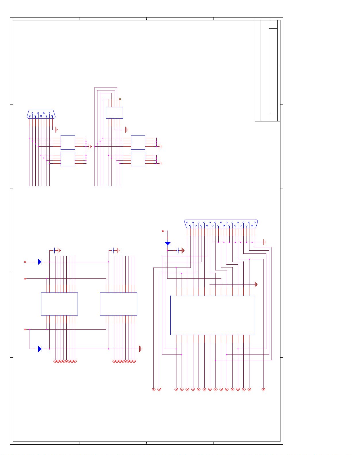
of
22 34Wednesday, March 27, 2002
E
D
C
COM1
COM1
DSR0
DCD0
RXDD0
RTS0
TXDD0
CTS0
DTR0
RI0
CONNECTOR_DB9
594837261
6
4
2
6
4
2
BC27
.1U
CN2
6
4
2
6
4
2
CN1
100PF/8P4C
7 8
7 8
5
5
3
3
1
1
7 8
7 8
5
5
3
3
1
1
100PF/8P4C
COM2
RXDD1
DTR1
CTS1
DSR1
COM2
DCD1
246
8
13579
TXDD1
RTS1
BC28
.1U
10
RI1
HEADER_5X2
CN4
6
6
4
4
2
2
6
6
4
4
2
2
CN3
100PF/8P4C
7 8
7 8
5
5
3
3
1
1
7 8
7 8
5
5
3
3
1
1
100PF/8P4C
VCC5
E
SERIAL AND PARALLEL PORT
<Doc> 0.5
Low Power Intel® Celeron®/Pemtium® III with 815E
Title
Size Document Number Rev
Date: Sheet
D
LPT1
1
SS12/SMD
BC29
.1U
D6
22921820719618517416315214
LPT
13251224112310
C
D5
SS12/SMD
DCD0
DTR0
CTS0
TXDD0
RTS0
RXDD0
DSR0
RI0
VCC12 VCC5
DY3
DA3
DTR#016
RA4
RY4
CTS#016
DY2
DA2
TXD016
DY1
DA1
RTS#016
RA3
RY3
RXD016
RA2
RY2
DSR#016
2345678
19181716151413
RA1
RY1
RI#016
GD75232
1
9
20
5V
12V
RA5
U13
-12V
GND
B
VCC12-
D4
A
RY5
101112
SS12/SMD
DCD#016
U14
1
20
5V
12V
-12V
GND
101112
DCD1
9
RA5
RY5
DCD#116
DTR1
DY3
DA3
DTR#116
CTS1
TXDD1
RA4
DY2
DA2
RY4
TXD116
CTS#116
RTS1
RXDD1
RA3
DY1
RY3
DA1
RXD116
RTS#116
DSR1
RA2
RY2
DSR#116
RI1
2345678
19181716151413
RA1
GD75232
RY1
U15
Parallel Port
RI#116
ERR#16
AFD#16
28
2715252423222120191817
P8
P7
SO2
P1P2SI1 SO1
123 26456789
PAR_INIT#16
SI2
PDR116
STB#16
PDR016
SLIN#16
SO5
SO3
SO4
GND
SI3
SI4
SI5P3SI6P4SI7P5SI8
PDR316
PDR416
SLCT16
PDR216
VCC
16
SO6
SO7
SO8
SO9
1011121314
PDR516
BUSY16
PE16
PDR616
P6
B
PAC-S1284
SI9
PDR716
ACK#16
A
4 4
3 3
2 2
1 1

of
23 34Wednesday, March 27, 2002
E
KEYBOARD, MOUSE, GAME & IR
Title
D
J4
GAME_PORT
815714613512411310291
Low Power Intel® Celeron®/Pemtium® III with 815E
Size Document Number Rev
E
<Doc> 0.5
Date: Sheet
D
C
2
4
6
2
4
6
C224
C223
C225
2
4
6
2
4
6
22PF
1000PF
470PF
Game Port
CN6
470PF/8P4C
1
1
3
3
5
5
7 8
7 8
1
1
3
3
5
5
7 8
7 8
CN5
C229
470PF
470PF/8P4C
C228
470PF
C227
22PF
C233
1000PF
C231
1000PF
C230
22PF
C232
1000PF
22PF
C226
FB14
0
R166
VCC5DUAL
470PF
F2 XFUSE_1.0A
FB13
C222
BEAD
R163
R162
R161
R160
R159
R158
1 2
4.7K
4.7K
4.7K
4.7K
4.7K
4.7K
R157 0
VCC5VCC5 VCC5VCC5 VCC5VCC5 VCC5
B
A
J2BUT1
J1BUT1
7
8
RN7 1K/8P4R
J1BUTTON116
JOY_2X
JOY_1X
135
246
JOY1X16
J2BUTTON116
MIDI_OUTPUT
47
RN8 1K/8P4R
R164
JOY2X16
MIDI_OUT16
JOY_1Y
JOY_2Y
7
8
JOY1Y16
JOY2Y16
J2BUT2
J1BUT2
135
246
J2BUTTON216
J1BUTTON216
MIDI_INPUT
R165 47
MIDI_IN16
BEAD
1 2
F3 XFUSE_1.0A
R167 0
U16
1234561314151617789101112
FB15
BEAD
FB16
BEAD
FB17
BEAD
7
8
RN9 4.7K/8P4R
FB18
1 2
135
246
1 2
F4 XFUSE_1.0A
KDAT16
1 2
KCLK16
KB/MOUSE
Keyboard
Mouse
C235
2.2UF
C234
2.2UF
135
FB19
78
BEAD
1 2
MCLK16
78
CN7
IR1
13245
VCC5
246
IRRX16
135
470PF8P4C
246
IR
HEADER_1X5
IRTX16
BEAD
1 2
MDAT16
C
B
A
4 4
3 3
2 2
1 1

of
24 34Wednesday, March 27, 2002
DIGITAL VIDEO OUT
<Doc> 0.5
Low Power Intel® Celeron®/Pemtium® III with 815E
Title
Size Document Number Rev
Date: Sheet
FPDV3
1K
A3_PD
6
CTL3/A3/DK3
VS
5
FTVSYNC9
R174A
R173A
4.7K
GND0
GND1
GND2
PGND
AGND0
AGND1
AGND2
1K
Do Not Stuff
A
16
48
64
17
20
26
32
1K
R171A
R172A
VCC3_3
12
A2_PD
TX0+ 25
TXC+ 25
TX0- 25
25
TX0-
TX0+
DFP
D17
D18
D16/PFEN
42
44
TX1- 25
28
27
TX1-
TX1+
Flat Panel
D13
D14
D15
1
12
33
18
49
23
29
3
U17A
Place C106A
near U8A pin 3
+
12
C246A
R170A
VCC0
VCC1
VCC2
PVCC0
PVCC1
AVCC0
AVCC1
VREF
36
C247A
1K
EXTRS_PU
D23
100pF
21
TXC- 25
TXC-
D22
0.01UF
24
22
TXC+
D20
D21
D19
393837
414043
L10A
10UF
+
12
C242A
A
C241A
C240A
C239A
100PF
100PF
100PF
R169A
1%
400
FPDV3
L9A
VCC3_3
FPP1V3
12
+
12
C236A
C238A
C237A
10UF
VCC3_3
FPAV3
100PF
100PF
12
L11A
VCC1_8
C243A
C245A
12
+
C244A
100PF
100PF
10UF
FTVREF
1K
R168A
TX2+ 25
TX2- 25
TX1+ 25
31
30
19
TX2-
TX2+
EXT_RS
Transmitter
D10
D11
D12
5150474645
FTD7
FTD8
FTD11
FTD10
FTD9
FTD[11:0]9
PCIRST# 7,15,16,32
TEST_PD
35
TEST
DKEN
FTD5
FTD4
FTD6
3VFTSCL 9,25
151434
BSEL/SCL
D3D4D5D6D7D8D9
60595855545352
FTD3
3VFTSDA 9,25
131110
DSEL/SDA
D2
62
61
FTD2
FTD1
SL_STALL9
MSEN
ISEL/RST
D0
D1
63
FTD0
PD
3VHTPLG25
9
EDGE/CHG
IDCLK-
57
56
FTCLK09
A1_PD
7
8
CTL2/A2/DK2
CTL1/A1/DK1
DE
IDCLK+
2
4
FTCLK19
FTBLNK#9
HS
FTHSYNC9
Digital Video Out
A A

of
25 34Wednesday, March 27, 2002
111
6
761112128
BAT54S
L14A
L_GREEN
1 2
3139
L_BLUE
C253A
BLM11B750S
C252A
R180A
L_HSYNC
75
J6A
1K
R175A
2.5A
CRT5V_F
VCC5
1 2
F5A
BLM11B750S is rated at
70Ohms at 100MHz
1K
R176A
L12A
1 2
C249A
BLM11B750S
C248A
R177A
3
BAT54S
CR1A
2
1
VCC1_8
Place R66A,R67A,&
R69A Close to VGA
Connector
A
L_RED
MONOPU
L13A
1 2
3.3PF
3.3PF
75
1%
3
CR3A
2
1
VCC1_8
15
10
5
4
14
10515
10PF
5VVSYNC
C262A
10PF
C261A
10PF
C260A
10PF
C259A
1 2
C264A
BLM11B750S
C263A
CR7A
VCC1_8
R186A
3.3PF
3.3PF
3
BAT54S
2
1
75
1%
3.3PF
C258A
0K
C257A
CR6A
VCC5
L15A
3.3PF
Do Not Stuff C117A and C118A
3
BAT54S
2
1
L_VSYNC
FUSE_5
MON2PU
3.3PF
3.3PF
R183A
3.3PF
C255A
0K
3.3PF
C254A
R185A
Do Not Stuff C114A and C115A
1%
3
CR4A
BAT54S
2
1
VCC5
5VHSYNC
5VDDCDA
5VDDCCL
VIDEO CONNECTORS
<Doc> 0.5
Low Power Intel® Celeron®/Pemtium® III with 815E
Title
Size Document Number Rev
Date: Sheet
A
VID_RED9
VID_GREEN9
VGA Connector
Protection Circuit
for 20V Tolerance
-
+
J5A
A C
1N5821
CR2A
TX2+ 24
TX2- 24
TX0+ 24
TX0- 24
15
111
13
6 16
2 1234 14
5
TX1+24
TX1-24
TXC +24
TXC -24
VCC5
20 Pin Flat Panel Connector
VCC5
R178A
7 17
2.2K
R179
12
CON_HTPLG 5VHTPLG
8 18
9 19
+
12
C251A
C250A
De-Bounce
30k
10 20
10UF
Circuit
VID_BLUE9
VCC5
AC
CR5A
4.7K
R184A
QS4_3V
0.1UF
C256A
6
7
8
RP1A
2.2K
4 5
3
2
1
U18A
24
QST3384
VCC
5VDDCDA
1B1
1A1
3
5VDDCCL
1A2 1B2
4 5
5VHSYNC
1B3
1A3
7
0.01UF
5VFTSDA
R181A
CON_FTSDA
CON_FTSCL
5VFTSCL
0K
0K
R182A
is also populated.
Populate if DFP Device
5VVSYNC
1B41A4
5VHTPLG
1B51A5
5VFTSCL
5VFTSDA
R187A
QSSDA
16151011986
2B2
2B1
2A1
2A2
18 19
141721
2A3 2B3
SMBDATA 11,12,14,16,31,32
SMBCLK 11,12,14,16, 31,32
0K
0K
R188A
QSSCL
23
20
12
2B5
2B4
GND
BEA#
BEB#
2A5
2A4
1
13222
2.2K
2.2K
R189A
R190A
Do Not Populate
5V to 3.3V Translation / Isolation
Video Connectors
3VFTSCL9,24
3VHTPLG24
3VFTSDA9,24
3VDDCCL9
3VDDCDA9
CRT_HSYNC9
CRT_VSYNC9
A A
CK_SMBCLK6
CK_SMBDATA6

1
C275
0.1uF
C274
0.1uF
of
1
26 34Wednesday, March 27, 2002
2
C273
0.1uF
R195
Place decoupling capacitors near
82562ET
C278
V3SB
46
X1
TESTEN
21
R194
R193
VSSR VCCR
VSSA2
VSSA
VSSP
VSSP
VSS
VSS
VSS
VSS
VSS
0
10K
+
C277
+
C276
+
Y4
20 23
6
38
48
24
18
8
82562ET
4.7uF
4.7uF
4.7uF
25MHz
C280
C279
22pF
22pF
C269
0.1uF
C268
C267
0.1uF
0.1uF
3
V3SB
6
4
V3SB
5
6
7
7
NC
NC
VCCGND
85
U19
EECS
EESK
EEDI
EEDO
123
4
EE_CS14
EE_SHCLK14
EE_DIN14
EE_DOUT14
C266
C265
BLM11B750S1A
1 2
V3SB
93C46
TDP
TDN
4.7uF
103311
TDP
4.7uF
TDN
VCCRVSSR
1922
VCCT
17
VCCT
14
VCCT
12
VCCT
9
VCCA2
7
VCCA
2
VCCP
36
VCCP
40
VCC
25
VCC
1
JTXD2
JRSTSYNC
JCLK
U20
45344
39
246
8
RP2
135
7
RDP
15
RDP
JTXD1
0
RP3
RDN
16
RDN
JTXD0
43
246
135
V3SB
JRXD2
37
4
5
RBIAS10
RBIAS100
JRXD1
JRXD0
35
34
8
7
C272
0.1uF
C271
0.1uF
C270
0.1uF
R192
R191
ACTLED
SPEEDLED
LILED
32
31
ACTLED
SPDLED
ADV10
ISOL_TCK
41
301329
0
549, 1%
619, 1%
27
LILED
ISOL_EX
ISOL_TI
28
47
X2
TOUT
26
330
V3SB
R196
AMBER
D8
GREEN
D7
330
RJ45
FRE
E5608-0E0045
J7
C1C2C3C4C5C6C7
1234567
TX+
CMT
U21
TDCNCNC
TD+
LILED
8
TX-
NC
NC
RX+
RXC
RD+
RDC
TD-
ACTLED
Place close to 82562ET
R198
R197
TDP
100, 1%
TDN
100, 1%
RDP
SH_1
SH_0
C8
RX-
RD-
RDN
SPEEDLED
12
11
H1102
C281
R202
R201
R200
R199
0.1uF
75, 1%
75, 1%
75, 1%
75, 1%
LAN ON MOTHERBOARD
Title
C282
1000pF, 2KV
Low Power Intel® Celeron®/Pemtium® III with 815E
Size Document Number Rev
2
<Doc> 0.5
Date: Sheet
3
4
5
6
7
8
LAN_CLK13
LAN_TXD213
LAN_TXD113
LAN_TXD013
LAN_RXD213
LAN_RXD113
LAN_RXD013
8
LAN_RSTSYNC13
D D
C C
B B
A A

of
27 34Wednesday, March 27, 2002
U22C
VCC5SBY
5 6
PWROK 14,16
74LVC06A
V3SBV3SB
U26A
U25A
1 2
RSMRST# 14,16
74LVC14A
7 14
74LVC14A
Do not stuff. For
debug only
1M
R210A
ATX POWER
<Doc> 0.5
Low Power Intel® Celeron®/Pemtium® III with 815E
Title
Size Document Number Rev
E
Date: Sheet
E
R204
4.7K
V3SB
V3SB
R209A
1 2
D
BC32
1.0uF
22k
C
D
VCC5SBY
U22A
33K
R205
C283
2UF
U22B
74LVC06A
7 14
1 2
VCC5SBY
15K
R203
D9
1N4148
C
VCC5SBY
BC30
.1U
21
U23A
V3SB
74LVC14A
VCC12
VCC5SBY
U23B
7 14
ATXPWROK
14
3 4
43
U24A
74LS132
74LVC14A
Y
VCC
A
1
74LVC06A
B
2
C284
VCC5SBY
BC31
1.0uF
Resume Reset Circuitry.
22msec delay
U22D
74LVC06A
9 8
65
U23C
74LVC14A
SW1
1 2
JP8
Reset button
Place JP near front panel hdr
.1U
3
V3SBV3SB
B
A
2345678910
1
3.3V
ATXPR1
3.3V
111213141516171819
VCC12-
VCC3_3 VCC5VCC5SBY
3.3V
-12V
GND
GND
+5V
PS_ON
PS_ON16
GND
GND
+5V
GND
GND
GND
VCC_5-
AUX5V
PWROK
-5V
+5V
20
VCC5
4 4
+12V
ATX_PWCON
+5V
R206 100
R207
1K
R208A
12
22
C285
C286
10uF
B
0.01uF
VCC5
A
HWRST#31
DBRESET#4
3 3
2 2
1 1

of
28 34Wednesday, March 27, 2002
VCC12-
-12VIN 16
232K,1%
VCC_5-
-5VIN 16
HARDWARE MONITOR
PR9
120K,1%
Title
Low Power Intel® Celeron®/Pemtium® III with 815E
Size Document Number Rev
E
<Doc> 0.5
Date: Sheet
E
t
X10K_1%-THRM/0603
RT1
"system use"
PR2
10K,1%
t
10K_1%-THRM/0603
RT2
"power use"
PR3
10K,1%
JP9
HEADER_2
2
1
+12VIN 16
VOLTAGE SENSING
R220
PR5
10K,1%
+3.3VIN 16
VTT 16
VCORE 16
PR7
R223
10K
R221
10K
10K
D
R215
PR4
30K
C287
3300PF
28K,1%
PR6
56K,1%
PR8
56K,1%
D
TEMPERATURE SENSING
VTIN116
VTIN316
C
FANIO1 16
CHASSIS FAN
R213
1K
VCC5
D10
B
1N4148
VTIN24,16
HM_VREF16
THRMDN4,16
VCC12
FANIO2 16
CPU FAN
R218
1K
VCC5
D11
1N4148
VCCT1_5
VCC_CORE
VCC5
VCC3_3
PWR FAN
R224
1K
D12
1N4148
C
FANIO3 16
B
132
FAN1
Q2
EC2
+
2N7002
22UF
510
FANPWM116
R214
3 3
HEADER_3
VCC12
R216
Q3
4.7K
+12CHFAN
Q1
2N2907
VCC12
1K
4.7K
R211
R212
A
4 4
+12CPUFAN
2N2907
1K
R217
FAN2
EC3
Q4
+
2N7002
132
22UF
510
R219
FANPWM216
HEADER_3
VCC12
EC4
R222 10M
VCCRTC
CASEOPEN#14,16
2 2
132
FAN3
+
22UF
If case is opened,
HEADER_3
S1
HEADER_2PIN
this switch should be closed.
A
1 1

of
Low Power Intel® Celeron®/Pemtium® III with 815E
Title
<Doc> 0.5
Size Document Number Rev
29 34Wednesday, March 27, 2002
E
Date: Sheet
D
VCC_CORE
+
R229
EC11
1000uF
10V
+
EC10
1000uF
10V
+
EC9
1000uF
10V
+
EC8
820uF
10V
+
EC7
820uF
10V
+
EC6
820uF
10V
+
EC5
820uF
10V
21
R232
220
21
3m
220
R230
21
E
C296
10uF
C295
0.1uF
C294
3300uF
L16 1.7uH
12
C293
3300uF
12
C292
C291
C290
4.7uF
4.7uF
4.7uF
D
21
R227
3m
Stuff only one
1uH
Q5
MOSFET N
L17
Q6
MOSFET N
C288
C289
0.1uF
0.1uF
C299
0.001uF 6.3V
+
EC15
+
EC14
+
EC13
+
EC12
1000uF
10V
1000uF
10V
1000uF
10V
1000uF
10V
Not Pop
VCC5
VCC_CLK_2_5 6
C304
10uF
+
2
PR10
100,1%
PR11
100,1%
VOUT
LM1117ADJ
ADJ
1
Q7
VIN
VOLTAGE REGULATOR PART 1
3
C303
10uF
+
C302
10uF
C
VCC12 VCC5
C301
0.1uF
C
2.2
R226
R228 2.2
2 1
2 1
201918171615141312
PGND
VID2
DRVH
VID1
DRVL
VID0
VCC
VID25
LRFB
PWRGD
U27
GND
VID3
123456789
R225
4m
1
0
000
1
1
2-11
3-10
2 1
1
0
0
0
0
5-8
4-9
B
1 : open
0 : close (GND)
0
1.10V
A
1.25V
1.35V
(Default)
Dip Switch
Pin #
0
1
1-12
COMP
LRDRV
REFSDFB
21
SW2
10
11
12
C297
180nF
6.3V
11
CT
CS+
ADP3170
CS-
10
C298
0.1uF
6.3V
R231
11.2k
DIP switch 6 position
6 7
5 8
4 9
3
2
1
C300
56k
R233
21
21
R238
100.
21
R237
100
21
R236
100
21
R235
100
21
R234
100
2.2nF
B
VRM_PWRGD14
VCCT1_5
Q8
2
VOUT
ADJ
VIN
C306
+
R239
LT1587-ADJ
1
10uF
49.9 1%
R240
10 1%
3
C305
10uF
+
VCC3_3
A
4 4
3 3
2 2
1 1

of
30 34Wednesday, March 27, 2002
E
VOLTAGE REGULATOR PART 2
EC25
2
3
VOUT
ADJ
VIN
10uF
+
PR14
LM1117ADJ
1
EC24
10uF
+
120,1%
PR15
60,1%
EC20
100uF
+
2
PR12
100,1%
PR13
D
LM1117ADJ
VOUT
ADJ
1
Q9
VIN
100,1%
V1_8SBV3SB
Q13
3
EC19
10uF
VCC5 VCC2_5
+
EC23
+
VCC3_3SBY
100uF
VCC5DUAL
VCC1_8VCC3_3
Q15
2
3
VOUT
ADJ
VIN
EC29
10uF
+
PR16
LM1117ADJ
1
EC28
10uF
+
120,1%
PR17
Title
60,1%
Low Power Intel® Celeron®/Pemtium® III with 815E
Size Document Number Rev
E
<Doc> 0.5
Date: Sheet
D
C
Q12
NDS356AP/SOT23
C
VCC5SBY
EC18
+
EC17
EC16
C307
100uF
+
10uF
+
100uF
0.1uF
VCC3_3VCC12VCC5SBY
B
Q10
U28
12V
14
1
HUF76121D3S/TO252
EC21
+
C308
15
16
DRV2
VSEN2
5VSB
3V3DLSB
3V3DL
FAULT/MSETS3S5
349
Q11
NZT651/SOT223
EC22
C309
+
1500uF
1uF
10K
R241
1uF
10uF
111012
5VDLSB
675
5VDL
EN5VDL
EN3VDL
2
13
C310
DLA
GND
SS
1uF
8
HIP6501
0.1uF
C311
Q14
6
G2 D2
3
4 5
7
8
D2D1D1
G1
S2
1
2
S1
FDS8936 / SI9936
EC27
+
100uF
EC26
+
100uF
B
A
4 4
V3SB
SLP_S5#14
SLP_S3#6,14,16
VCC5SBY
3 3
VCC3_3
VCC5
2 2
1 1
A

KEYLOCK
HDD LED
PN1
12345678910111213
PWR_SW
SMI_SW
14
HEADER_14
of
31 34Wednesday, March 27, 2002
E
R246
220
V3SB VCC5VCC5SBY
R245
R244
R243
R242
150
SMB2
10K
220
10K
R251
0
D13 1N4148
D14 1N4148
C312
0.1uF
SMB1
13245
13245
SMBCON
SMBCON
D15
LED
FRONT PANEL AND SMBUS
Title
Low Power Intel® Celeron®/Pemtium® III with 815E
Size Document Number Rev
E
<Doc> 0.5
Date: Sheet
VCC5 VCC5
D
EXTSMI#13
KEYLOCK#16
BC33
0.1uF
R250
10K
SMBDATA11,12,14,16,25,32
SMBCLK11,12,14,16,25,32
PANSWIN16
IDEACTS#15
IDEACTP#15
R259 330
VCC5SBY
D
C
GREEN LED
SPEAKER
RESET
PN2
12345678910111213
RESERVE
14
SP1
HEADER_14
BUZZER
C
VCC5
R253
VCC5
R252
0
Q16
R249
150
VCC5SBY
B
R248
10K
2N3904
33
BC34
0.1uF
R255 68
R256 68
Q18
Q17
2N3904
2N3904
MIXED IN ON_BOARD AC97 CODEC
ON BOARD BUZZ OR DIRECT TO SPKR
TRADITIONAL PC SOUND
JP8
3-4 ON
1-2 ON
B
R257 2.2K
R247
10K
VCC5
VCC5
R254
10K
JP10
XHEADER 2X2
1 2
3 4
R258 0
A
HWRST#27
4 4
SUSLED16
3 3
ICH_SPKR14,32
BEEP16
AC97SPKR20
2 2
1 1
A

of
32 34Wednesday, March 27, 2002
E
R260
IDERST# 15
1K
VCC3_3
VCC3_3 VCC5
147
VCC3_3
U29A
74LVC07A
1 2
R261
1K
U29B
147
3 4
PCI_RST# 17,18
VCC3_3
74LVC07A
R264
1K
U29D
147
9 8
PCIRST# 7,15,16,24
74LVC07A
U23D
89
74LVC14A
U23E
1011
74LVC14A
PULL-UP RESISTORS
Title
BC35
.1U
VCC3_3
D
VCC3_3
VCC3_3 VCC3_3
R263
1K
U29C
147
74LVC07A
VCC3_3
U29E
74LVC07A
147
11 10
VCC3_3
U29F
74LVC07A
147
13 12
Low Power Intel® Celeron®/Pemtium® III with 815E
Size Document Number Rev
E
<Doc> 0.5
Date: Sheet
D
5 6
U22E
ICHRST#13
VCC5SBY
11 10
74LVC06A
C
V3SB
V3SB
VCC3_3
VCC3_3
V3SB
VCC3_3
VCC5SBY
U22F
74LVC06A
13 12
C
B
A
VCC5 V3SB
PCI ICH
RN10
RP4
246
135
SMBALERT#14
5
1234678
PERR#13,17,18
8
4.7K/8P4R
RN11
7
SMBDATA11,12,14,16,25,31
SMBCLK11,12,14,16,25,31
10
C
C
R1R2R3R4R5R6R7
SERR#13,17,18
PLOCK#13,17,18
STOP#13,17,18
DEVSEL#13,17,18
IRDY#13,17,18
TRDY#13,17,18
246
135
LPC_PME#13,16
R8
9
FRAME#13,17,18
8
4.7K/8P4R
7
SMLINK114,18
SMLINK014,18
246
RN12
2.7K/10P8R
135
PREQ#213,18
RN13
PREQ#113,17
246
135
GPI813
8
7
PREQ#013,17
8
7
GPIO2813
GPIO2713
GPIO2514
RN14
2.7K/8P4R
8.2K/8P4R
246
135
PREQ#313,18
PREQ#513
RN15
PREQ#413
246
135
PCI_REQ#A13
8
7
ACK64#17,18
KBRST#13,16
OVT#14,16
2.7K/8P4R
8
7
A20GATE13,16
RN16
8.2K/8P4R
246
135
REQ64#217
REQ64#117
R265 10K
R262 8.2K
Do not populate
AC_SDIN014,20
SERIRQ13,16
8
2.7K/8P4R
7
REQ64#418
REQ64#318
R266 10K
AC_SDIN114
VCC3_3
R267 1.8K
AC_RST#14,20
JP11
R268 8.2K
AC_SDOUT14,20
R269 8.2K
ICH_RI#14
JP12
R270 2.7K
ICH_SPKR14,31
RN17
246
135
PIRQ#C13,17,18
PIRQ#A13,17,18
PIRQ#B13,17,18
8
7
PIRQ#D13,17,18
8.2k
RN18
246
135
PIRQ#E13
8
8.2k
7
B
A
PIRQ#G13
PIRQ#F13
PIRQ#H13
JP1
OFF : Normal CPU freq strap (default)
ON : Force CPU freq strap safe mode
JP5
OFF : Reboot on TCO timer timeout (default)
ON: No reboot on TCO timer timeout
4 4
3 3
2 2
1 1

V3SB
3
U31A
147
1
SN74LVC08A
2
6
U31B
147
4
SN74LVC08A
5
of
33 34Wednesday, March 27, 2002
UNUSED GATES
<Doc> 0.5
Low Power Intel® Celeron®/Pemtium® III with 815E
Title
Size Document Number Rev
Date: Sheet
U33A
74LS132
3
Y
GND VCC
7 14
A
VCC5SBY
B
1
2
6
U33B
74LS132
Y
GND VCC
7 14
A
B
4
5
U26C
74LVC14A
7 14
A O
U32A
SN74LVC06A
GND VCC
21
OA
74LVC14A
5 6
7 14
SN74LVC07A
GND VCC
7 14
7 14
U34A
147
V3SB
U30B
SN74LVC06A
A O
3 4
43
U32B
1 2
GND VCC
OA
SN74LVC07A
7 14
SN74LVC07A
GND VCC
7 14
U34B
147
3 4
U30C
5 6
U32C
A O
65
SN74LVC07A
SN74LVC06A
OA
U34C
147
5 6
GND VCC
7 14
SN74LVC07A
GND VCC
7 14
A
SN74LVC07A
U26B
V3SB
3 4
A
U30A
V3SB
1 2
VCC3_3
UNUSED GATES
A A
of
34 34Wednesday, March 27, 2002
E
D
C
B
A
BC43
BC42
BC41
BC40
" ATX POWER "" ATX POWER "
EC31
VCC12-VCC12
BC39
BC38
BC37
BC36
EC30
" ATX POWER " " ATX POWER " " ATX POWER "
VCC3_3 VCC5 VCC_5-
BC49
BC48
EC34
BC47
BC46
EC33
BC45
BC44
EC32
0.1UF
0.1UF
0.1UF
0.1UF
0.1UF
0.1UF
0.1UF
0.1UF
22UF
" Display Cache : Near the Power Pins "
VCC3_3
22UF
0.1UF
0.1UF
22UF
0.1UF
0.1UF
22UF
0.1UF
0.1UF
22UF
VCCVID
4 4
BC57
BC56
BC55
BC54
BC53
BC52
BC51
BC50
MC36
MC35
MC34
MC33
MC32
MC31
MC30
MC29
MC28
MC27
MC26
MC25
MC24
MC23
MC22
MC21
0.1UF
0.1UF
0.1UF
0.1UF
0.1UF
0.1UF
0.1UF
0.1UF
4.7UF
4.7UF
4.7UF
4.7UF
4.7UF
4.7UF
4.7UF
4.7UF
4.7UF
4.7UF
4.7UF
4.7UF
4.7UF
4.7UF
4.7UF
4.7UF
BC69
0.1UF
BC68
0.1UF
BC67
0.1UF
BC66
0.1UF
BC65
0.1UF
BC64
0.1UF
MC44
4.7UF
MC43
4.7UF
MC42
4.7UF
MC41
4.7UF
BC63
0.1UF
BC62
0.1UF
BC61
0.1UF
BC60
0.1UF
BC59
0.1UF
BC58
0.1UF
MC40
4.7UF
MC39
4.7UF
" DIMM0 : Near Power Pins " " DIMM1 : Near Power Pins "
MC38
4.7UF
MC37
4.7UF
VCC3_3SBY VCC3_3SBY
" ICH2 : Near Power Pins
V1_8SB
BC85
0.01UF
" ICH2 : Near Power Pins
VCC1_8V3SBVCC3_3
BC84
0.01UF
BC83
0.01UF
BC82
BC81
BC80
BC79
BC78
BC77
0.01UF
0.01UF
0.01UF
0.01UF
0.01UF
0.1UF
BC100
0.01UF
BC99
0.01UF
BC98
0.01UF
0.01UF
0.01UF
0.01UF
" ICH2 : Near Power Pins
BC97
BC96
" Within 70 mils of GMCH "
" GMCH : Near Display Cache Quadrant "
BC95
VCC3_3
BC76
BC75
BC74
BC73
BC72
BC71
0.1UF
0.1UF
0.1UF
0.1UF
0.1UF
0.1UF
BC94
BC93
BC92
BC91
BC90
BC89
0.01UF
0.01UF
0.01UF
0.01UF
0.01UF
0.01UF
" ICH2 : 0.1U//0.01U at each conner
BC70
0.1UF
MC46
MC45
4.7UF
4.7UF
" GMCH : 0.1U//0.01U at each conner and each side-center "
VCC1_8
3 3
BC88
0.01UF
" GMCH : Near System Mem Quadrant "
BC87
0.01UF
BC86
0.01UF
VCC3_3SBY
E
BC120
0.1UF
DECOUPLING CAPACITORS
<Doc> 0.5
BC119
BC118
0.1UF
0.1UF
Low Power Intel® Celeron®/Pemtium® III with 815E
Title
Size Document Number Rev
Date: Sheet
"
BC117
0.1UF
BC116
0.1UF
BC140
BC139
BC138
BC137
BC136
BC135
BC134
BC133
BC132
BC131
BC130
BC129
BC128
BC127
BC126
BC125
BC124
0.01UF
0.01UF
0.01UF
0.01UF
0.01UF
0.01UF
0.01UF
0.01UF
0.01UF
0.01UF
0.01UF
0.01UF
0.1UF
0.1UF
0.1UF
0.1UF
0.1UF
H6 HOLE A
123
H5 HOLE A
123
H4 HOLE A
123
H3 HOLE A
123
H2 HOLE A
123
678
4 5
678
4 5
678
4 5
678
4 5
678
4 5
BC115
0.1UF
BC114
0.1UF
"
BC113
0.1UF
BC112
0.1UF
BC111
0.1UF
BC110
0.1UF
BC109
0.1UF
MC50
2.2UF
"
MC49
2.2UF
BC108
0.01UF
BC107
0.01UF
BC106
0.01UF
BC105
0.01UF
BC104
0.1UF
BC103
0.1UF
BC102
0.1UF
"
BC123
BC101
0.1UF
0.1UF
D
C
B
A
678
BC122
" misc. "
VCC3_3
BC121
0.1UF
0.1UF
H1 HOLE A
123
1 1
4 5
MC48
2.2UF
MC47
2.2UF
2 2

Reference Schematic
R
This page intentionally left blank
66 Intel® Pentium® III and Intel Celeron® – Low Power/Ultra Low Power / 815E Design Guide
 Loading...