

Page 1

Celeron™ Processor
Development Kit Manual
July 1999
Order Number: 273246-002
Page 2

Information in this document is provided in connection with Intel products. No license, express or implied, by estoppel or otherwise, to any intellectual
property rights is granted by this document. Except as provided in Intel’s Terms and Conditions of Sale for such products, Intel assumes no liability
whatsoever, and Intel disclaims any express or implied warranty, relating to sale and/or use of Intel products including liability or warranties relating to
fitness for a particular purpose, merchantability, or infringement of any patent, copyright or other intellectual property right. Intel products are not
intended for use in medical, life saving, or life sustaining applications.
Intel may make changes to specifications and product descriptions at any time, without notice.
Designers must not rely on the absence or characteristics of any features or instructions marked “reserved” or “undefined.” Intel reserves these for
future definition and shall have no responsibility whatsoever for conflicts or incompatibilities arising from future changes to them.
The Celeron™ processor may contain design defects or errors known as errata which may cause the product to deviate from published specifications.
Current characterized errata are available on request.
MPEG is an international standard for video compression/decompression promoted by ISO. Implementations of MPEG CODECs, or MPEG enabled
platforms may require licenses from various entities, including Intel Corporatio n.
Contact your local Intel sales office or your distributor to obtain the latest specifications and before placing your product order.
Copies of documents which have an ordering number and are referenced in this document, or other Intel literature may be obtained by calling 1-800-
548-4725 or by visiting Intel's website at http://www.intel.com.
Copyright © Intel Corporation, 1999. Portions of this manual Copyright © 1999 General Software, Inc. All rights reserved.
*Third-party brands and names are the property of their respective owners.
Celeron™ Processor De velopment Kit Manual
Page 3

Contents
1 About This Manual ..................................................................................................1-1
1.1 Content Overview...............................................................................................1-1
1.2 Text Conventions ...............................................................................................1-1
1.3 Technical Support ..............................................................................................1-2
1.3.1 Electronic Support Systems ........................................ ...... ....... ...... ...1-2
1.3.1.1 Online Documents ...............................................................1-2
1.3.1.2 Intel Product Forums ...........................................................1-3
1.3.2 Telephone Technical Support ........... ...... ....... ...... ....... ...... ....... ...... ...1-3
1.4 Product Literature...............................................................................................1-3
1.5 Related Documents............................................................................................1-4
2 Getting Started ......................................................... ....................................... .........2-1
2.1 Overview ............................................................................... .............................2-1
2.1.1 Processor Assembly Features ..........................................................2-1
2.1.2 Baseboard Features..........................................................................2-2
2.2 Included Hardware .............................................................................................2-2
2.3 Software Key Features.......................................................................................2-3
2.3.1 General Software, Inc........................................................................2-3
2.3.2 QNX Software Systems, Ltd..............................................................2-4
2.4 Before You Begin ...............................................................................................2-4
2.5 Setting up the Evaluation Board.........................................................................2-5
2.6 Configuring the BIOS .........................................................................................2-7
3 Theory of Operation...............................................................................................3-1
3.1 Block Diagram....................................................................................................3-1
3.2 System Operation...............................................................................................3-2
3.2.1 Celeron Processor ................................... ....... ...... ....... ...... ....... ...... ...3-2
3.2.2 82443BX Host Bridge/Controller .............................................. .........3-2
3.2.2.1 System Bus Interface...........................................................3-3
3.2.2.2 Accelerated Graphics Port (AGP) Interface.........................3-3
3.2.2.3 System Clocking..................................................................3-3
3.2.3 ITP.....................................................................................................3-3
3.2.4 82371EB PCI to ISA/IDE Xcelerator (PIIX4E)...................................3-4
3.2.5 DRAM................................................................................................3-4
3.2.6 Power ................................................................................................3-4
3.2.7 Boot ROM..........................................................................................3-4
3.2.8 RTC/NVRAM.....................................................................................3-4
3.2.9 Legacy I/O...................... ...... ...... ....... ...... ....... ...... ....... ......................3-4
3.2.10 IDE Support.......................................................................................3-5
3.2.11 Floppy Disk Support ..........................................................................3-5
3.2.12 Keyboard/Mouse ...............................................................................3-5
3.2.13 USB...................................................................................................3-5
3.2.14 RS232 Ports................... ...... ...... ....... ...... ....... ...... ....... ...... ....... ...... ...3-5
3.2.15 IEEE 1284 Parallel Port.....................................................................3-5
3.2.16 PCI Connectors.................................................................................3-5
3.2.17 ISA Connectors .................................................................................3-5
3.2.18 AGP Connector .................................................................................3-5
Celeron™ Processor Development Kit Manual
iii
Page 4

3.2.19 Post Code Debugger.........................................................................3-6
3.2.20 Cloc k Ge neration .. ...... ....... ...................................... ....... ...... ....... ......3-6
3.2.21 Interrupt Map.....................................................................................3-6
3.2.22 Memory Map .....................................................................................3-7
4 Hardware Reference .................................... ....................................... ...................4-1
4.1 Processor Assembly .......................... ...... ...... ....... ...... ....... ...... ..........................4-1
4.1.1 Thermal Management .......................................................................4-1
4.1.2 ITP Debugger Port ............................................................................4-1
4.2 Post Code Debugger..........................................................................................4-1
4.3 ISA and PCI Expansion Slots.............................................................................4-2
4.4 PCI Device Mapping ..........................................................................................4-2
4.5 Connector Pinouts..............................................................................................4-3
4.5.1 ATX Power Connector.......................................................................4-3
4.5.2 ITP Debugger Connector ..................................................................4-4
4.5.3 Stacked USB.....................................................................................4-4
4.5.4 Mouse and Keyboard Connectors.....................................................4-5
4.5.5 Parallel Port.......................................................................................4-5
4.5.6 Serial Ports........................................................................................4-6
4.5.7 IDE Connector...................................................................................4-6
4.5.8 Floppy Drive Connector.....................................................................4-7
4.5.9 PCI Slot Connector............................................................................4-8
4.5.10 IS A Slot Conne cto r..... ....... ...... ...... ....... ....................................... ......4-9
4.6 AGP Connector.............. ....... ...... ....... ...... ...... ....... ...... ....... ...... ........................4-10
4.7 Jumpers ...... ...... ....... ...... ....................................... ...... ....... ...... ....... ...... ....... ....4-11
4.7.1 Enable Spread Spectrum Clocking (J14)........................................4-11
4.7.2 Clock Frequency Selection (J15) ....................................................4-11
4.7.3 On/Off (J20).....................................................................................4-11
4.7.4 Flash BIOS VPP Select (J21)..........................................................4-12
4.7.5 Flash BIOS Boot Block Control (J22)..............................................4-12
4.7.6 SMI# Source Control (J23)..............................................................4-12
4.7.7 CMOS RAM Clear (J24)..................................................................4-12
4.7.8 Push Button Switches .....................................................................4-12
4.8 In-Circuit BIOS Update.....................................................................................4-13
5 BIOS Quick Reference .......................................................... ................................5-1
5.1 BIOS and Pre-Boot Features.............................................................................5-1
5.2 Power-On Self-Test (POST) .................... ...... ....... ...... ....... ...... ....... ...... ....... ......5-1
5.3 Setup Screen System ........................................................................................5-3
5.3.1 Basic CMOS Configuration Screen...................................................5-3
5.3.2 Configuring Drive Assignments.........................................................5-4
5.3.2.1 Configuring Floppy Drive Types ..........................................5-4
5.3.3 Configuring IDE Drive Types.............................................................5-5
5.4 Configuring Boot Actions....................................................................................5-6
5.5 Custom Configuration Setup Screen..................................................................5-6
5.6 Shadow Configuration Setup Screen.................................................................5-7
5.7 Standard Diagnostics Routines Setup Screen ...................................................5-8
5.8 Start System BIOS Debugger Setup Screen .....................................................5-8
5.9 Start RS232 Manufacturing Link Setup Screen .................................................5-9
5.10 Manufacturing Mode ..........................................................................................5-9
iv
Celeron™ Processor De velopment Kit Manual
Page 5

5.10.1 Console Redirection ..........................................................................5-9
5.10.2 CE-Ready Windows CE Loader ......................................................5-10
5.10.3 Integrated BIOS Debugger..............................................................5-10
5.11 Embedded BIOS POST Codes........................................................................5-12
5.12 Embedded BIOS Beep Codes..........................................................................5-15
A PLD Code Listing................................................................................................... A-1
B Bill of Materials....................................................................................................... B-1
C Schematics ...............................................................................................................C-1
Index .................................................................................................................................Index-1
Figures
2-1 Evaluation Board Jumpers and Connectors.......................................................2-5
3-1 Evaluation Board Block Diagram........................................................................3-1
5-1 BIOS POST Pre-Boot Environment....................................................................5-2
5-2 Embedded BIOS Setup Screen Menu................................................................5-3
5-3 Embedded BIOS Basic Setup Screen................................................................5-4
5-4 Embedded BIOS Custom Setup Screen ............................................................5-7
5-5 Embedded BIOS Shadow Setup Screen............................................................5-7
5-6 Standard Diagnostic Routines Setup Screen.....................................................5-8
5-7 Start RS232 Manufacturing Link Setup Screen..................................................5-9
5-8 CE-Ready Boot Feature...................................................................................5-10
5-9 Integrated BIOS Debugger Running Over a Remote Terminal........................5-11
Tables
1-1 Related Documents............................................................................................1-4
3-1 Interrupts............................................................................................................3-6
3-2 Memory Map ......................................................................................................3-7
4-1 PCI Device Mapping...........................................................................................4-2
4-2 Primary Power Connector (J11).........................................................................4-3
4-3 ITP Connector Pin Assignment (J2 on the Processor Assembly) ......................4-4
4-4 USB Connector Pinout (J2)................................................................................4-4
4-5 Keyboard and Mouse Connector Pinouts (J1 on the Baseboard)......................4-5
4-6 DB25 Parallel Port Connector Pinout (J3)..........................................................4-5
4-7 Serial Port Connector Pinout (J4).......................................................................4-6
4-8 PCI IDE1 (JP3) and IDE2 (JP4) Connector........................................................4-6
4-9 Diskette Drive Header Connector (JP1).............................................................4-7
4-10 PCI Slots (J7, J8, J9)..........................................................................................4-8
4-11 ISA Slots (J5, J6)................................................................................................4-9
4-12 AGP Slot (J13) .................................................................................................4-10
4-13 Default Jumper Settings...................................................................................4-11
5-1 IDE0-IDE3 Drive Assignments...........................................................................5-5
B-1 Baseboard Bill of Materials................................................................................ B-1
B-2 Celeron™ Processor Assembly Bill of Materials............................................... B-5
Celeron™ Processor Development Kit Manual
v
Page 6

Page 7

About This Manual
This manual tells you how to set up and us e the eval uati on board and pr oces sor ass embly i nclu ded
in your Celeron™ Processor Development Kit.
1.1 Content Overview
Chapter 1, “About This Manual” - This chapter contains a description of conventions used in this
manual. The last few sections tell you how to obtain literature and contact customer support.
Chapter 2, “Getting Started” - Provides complete instructions on how to configure the evaluation
board and processor assembly by setting jumpers, connecting peripherals, providing power, and
configuring the BIOS.
Chapter 3, “Theory of Operation” - This chapter provides information on the system design.
Chapter 4, “Hardware Reference” - This chapter provides a description of jumper settings and
functions, and pinout information for each connector.
Chapter 5, “BIOS Quick Reference” - This chapter describes how to configure the BIOS for your
system configuration. A summary of all BIOS menu options is provided.
Appendix A, “PLD Code Listing” - This appe ndix i nclud es a sample code li stin g for t he Post Code
Debugger .
1
Appendix B, “Bill of Materials” - This appendix contains the bill of materials for the evaluation
board.
Appendix C, “Schematics” - This appendix contains schematics for selected connectors and
subsystems for the evaluation board.
1.2 Text Conventions
The following notations may be used throughout this manual.
# The pound symbol (#) appended to a signal name indicates that the
signal is active low.
Variables Variables are shown in italics. Variables must be replaced with correct
values.
Instructions Instruction mnemonics are shown in uppercase. When you are
programming, instructions are not case-sensitive. You may use either
upper- or lowercase.
Celeron™ Processor Development Kit Manual
1-1
Page 8

About This Manual
Numbers Hexadecimal numbers are represented by a string of hexadecimal digits
Units of Measure The following abbreviations are used to represent units of measure:
followed by the character H. A zero prefix is added to numbers that
begin with A through F. (For example, FF is shown as 0FFH.) Decimal
and binary numbers are represented by their customary notations. (That
is, 255 is a decimal number and 1111 1111 is a binary number. In some
cases, the letter B is added for clarity.)
Aamps, amperes
Gbyte gigabytes
Kbyte kilobytes
KΩ kilo-ohms
mA milliamps, milliamperes
Mbyte megabytes
MHz megahertz
ms milliseconds
mW milliwatts
ns nanoseconds
pF picofarads
Wwatts
Vvolts
µA microamps, microamperes
µF microfarads
µs microseconds
µW microwatts
Signal Names Signal names are shown in uppercase. When several signals share a
common name, an individual signal is represented by the signal name
followed by a number, while the group is represented by the signal name
followed by a variable (n). For example, the lower chip-select signals
are named CS0#, CS1#, CS2#, and so on; they are collectively called
CSn#. A pound symbol (#) appended to a signal name identifies an
active-low signal. Port pins are represented by the port abbreviation, a
period, and the pin number (e.g., P1.0).
1.3 Technical Support
1.3.1 Electronic Support Systems
Intel’s site on the World Wide Web (http://www.intel.com/) provides up-to-date technical
information and product support. This information is available 24 hours per day, 7 days per week,
providing technical information whenever you need it.
1.3.1.1 Online Documents
Product doc umentation is pro vided online in a v ariety of web-friendly formats at:
http://developer.intel.com/design/litcentr/index .htm
1-2
Celeron™ Processor Development Kit Manual
Page 9

1.3.1.2 Intel Product Forums
Intel provides technical expertise through electronic messaging. With publicly accessible forums,
you have all of the benefits of email technical support, with the added benefit of the option of
viewing previous messages written by other participants, and providing suggestions and tips that
can help others.
Each of Intel’s technical support forums is based on a single product or product family. Questions
and replies are limited to the topic of the particular forum. Intel also provides several non-technical
support related forums.
Complete information on Intel forums is available at:
http://support.intel.com/newsgroups/index.htm
1.3.2 Telephone Technical Support
In the U.S. and Canada, technical support representatives are available to answer your questions
between 5 a.m. and 5 p.m. PST. You can also fax your questions to us. (Please include your voice
telephone number and indicat e whether you prefer a response b y phone or b y fax). Outside the U.S .
and Canada, please contact your local distributor.
About This Manual
1-800-628-8686 U.S. and Canada
916-356-7599 U.S. and Canada
916-356-6100 (fax) U.S. and Canada
1.4 Product Literature
You can order product literature from the following Intel literature centers.
1-800-548-4725 U.S. and Canada
708-296-9333 U.S. (from overseas)
44(0)1793-431155 Europe (U.K.)
44(0)1793-421333 Germany
44(0)1793-421777 France
81(0)120-47-88-32 Japan (fax only)
Celeron™ Processor Development Kit Manual
1-3
Page 10
About This Manual
1.5 Related Documents
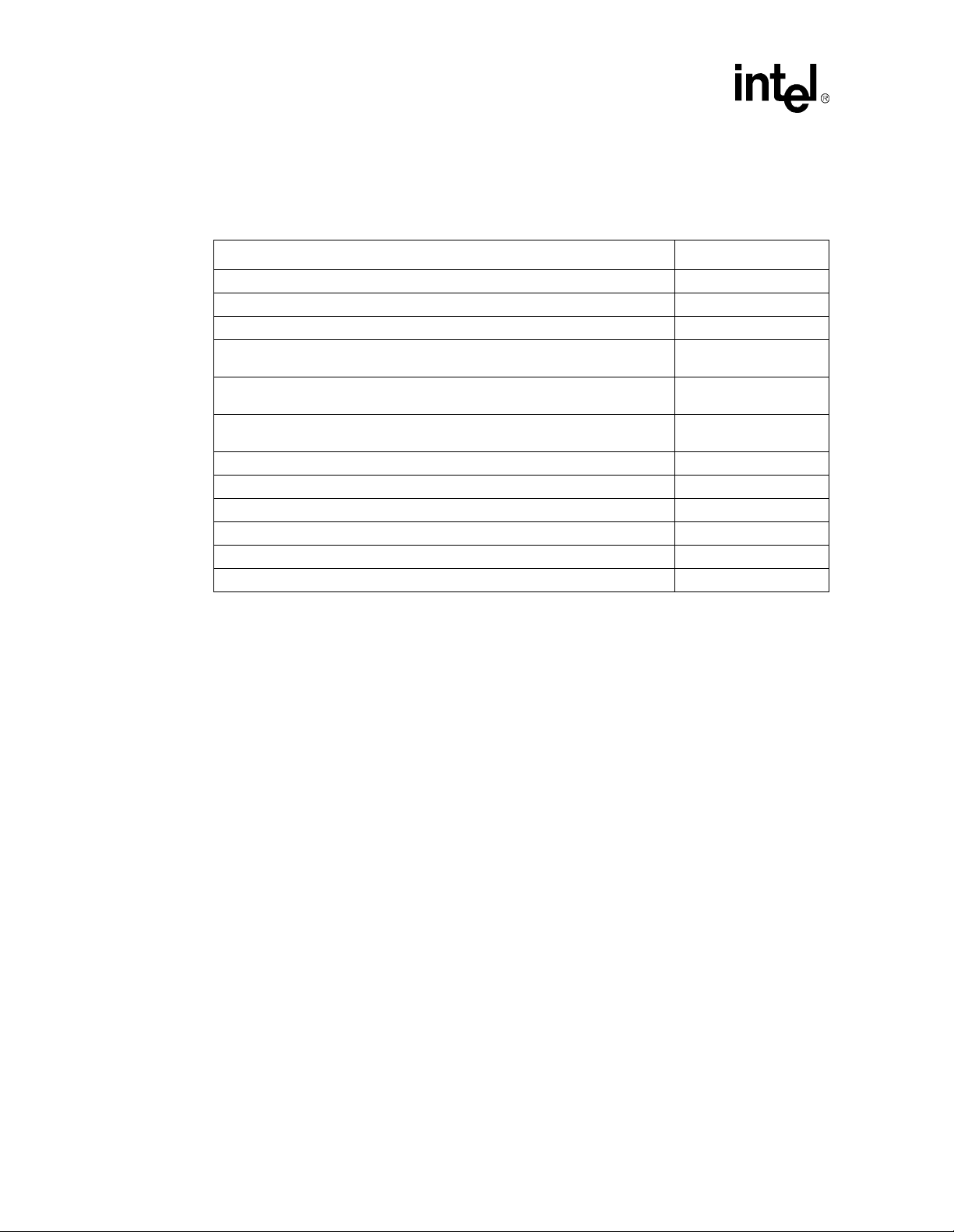
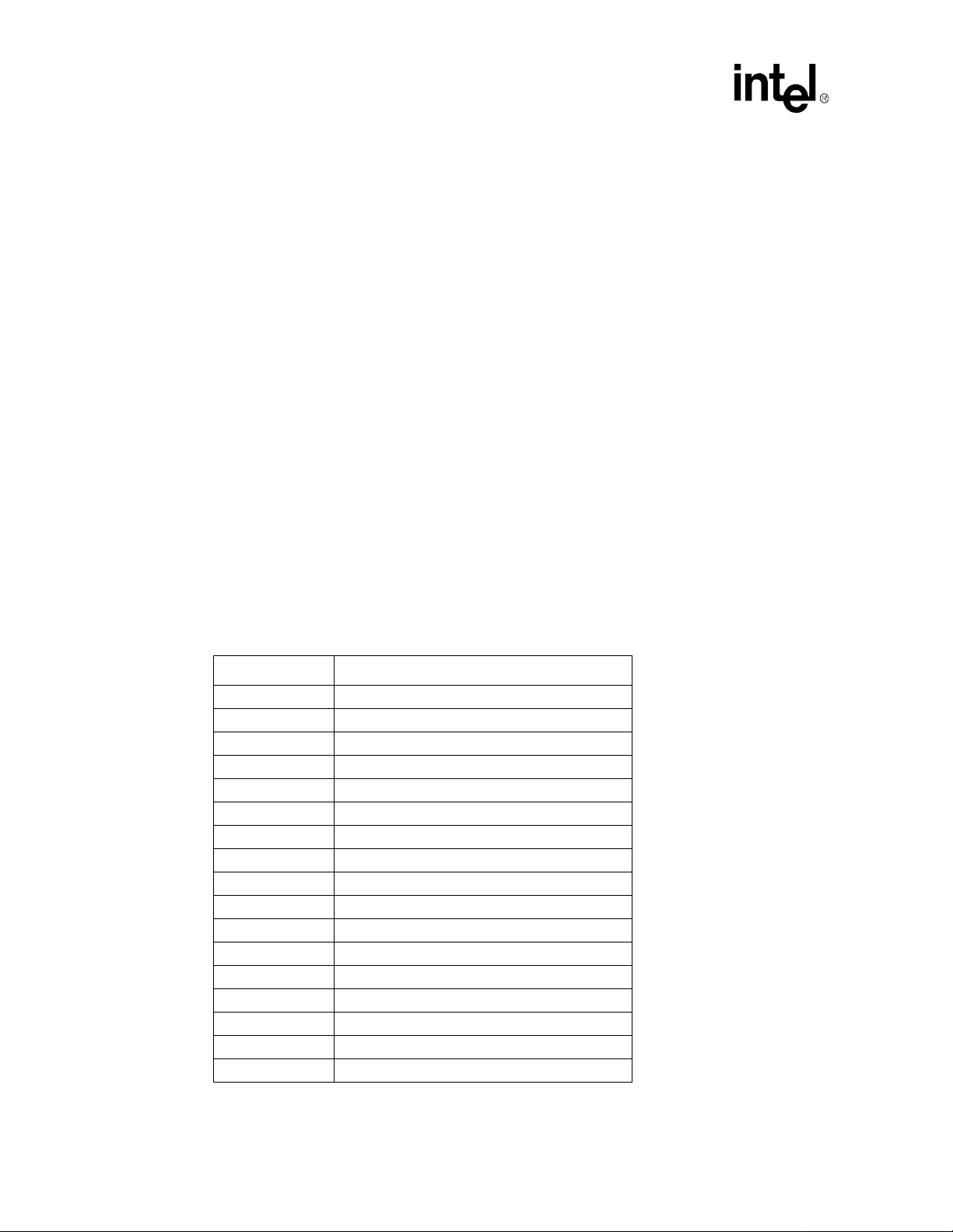
Table 1-1. Related Documents
Document Title Order Number
Intel® Celeron™ Processor
Intel® Celeron™ Processor Specification Update
P6 Family of Processors Hardware Developer’s Manual
Intel Architecture Software Developer’s Manual,
Volume 1: Basic Architecture
Intel Architecture Software Developer’s Manual,
Volume 2: Instruction Set Reference
Intel Architecture Software Developer’s Manual,
Volume 3: System Programming Guide
Intel® 440BX AGPset: 82443BX Host Bridge/Controller
Intel® 440BX AGPset: 82443BX Host Bridge/Controller Specification Update
Intel® 440BX AGPset: 82443BX Host Bridge/Controller Timing Specification
82371AB (PIIX4) and 82371EB (PIIX4E) PCI-TO-ISA/IDE Xcelerator
Intel 82371EB (PIIX4E) Specification Update
Intel 82371AB PCI ISA IDE Xcelerator (PIIX4) Timing Specification
datasheet 243658
datasheet 290633
datasheet 290562
243748
244001
243190
243191
243192
290639
273218
290635
273135
1-4
Celeron™ Processor Development Kit Manual
Page 11

Getting Started
This chapter identifies the Development Kit’s key components, features and specifications, and
tells you how to set up the board for o peratio n.
2.1 Overview
The evaluation board consists of a baseboard and a processor assembly.
• The processor assembly contains an Intel
Bridge/Controller.
• The baseboard contains the 82371EB PCI ISA IDE Xcelerator (PIIX4E) and other system
board components and peripheral connectors.
Warning: The processor assembly is attached to the baseboard at the factory. Do not remove the processor
assembly from the baseboard. Intel will not support the processor assembly or the baseboard if any
portion of the assembly is removed by the customer.
2.1.1 Processor Assembly Features
The processor assembly features are summarized below.
®
Celeron™ Processor and an 82443BX Host
2
• Celeron Processor in a PPGA package (Socket-370) with 66-MHz system bus frequencies
• Intel 440BX AGPset: 82443BX Host Bridge/Controller
• 66 MHz memory interface: A wide range of DRAM support including:
— 64-bit memory data interface plus 8 ECC bits and hardware scrubbing
— 60 ns EDO DRAM and 66 MHz SDRAM support
— 16 Mbit and 64 Mbit DRAM technologies
• Five PCI masters
— PCI Specification Rev 2.1 Compliant
• Accelerated Graphics Port (AGP) Support:
— AGP Interface Specification Revision 1.0 compliant
— AGP - 66/133 MHz, 3.3-V device support
• Integrated System Power Management support
Celeron™ Processor Development Kit Manual
2-1
Page 12

Getting Started
2.1.2 Baseboard Features
The baseboard has these features:
• Flash system BIOS ROM
— General Software system BIOS
— In-circuit BIOS upgradability
• Two SDRAM DIMM connectors
• 32-Mbyte SDRAM DIMM included
— 4 Mbyte x64, 3.3 V, 66 MHz with a CAS latency of 2
• User-accessible on-board connectors include:
— Two serial RS-232 ports; COM1, COM2
— One EPP/ECP parallel port
— PS/2 keyboard and PS/2 mouse (6-pin mini-DIN connectors)
— Two USB ports
— Two IDE bus connectors
— One floppy connector
— Three PCI expansion slots and two ISA expansion slots. There are no shared slots; all
slots are usable.
— One AGP connector
— Standard ATX power supply connector
• Miscellaneous features include:
— On board post-code debugger (Port 80)
— Reset push button
— Stand-off feet for table-top operation
2.2 Included Hardware
• Evaluation board (baseboard and processor assembly combination)
• 3.2-Gbyte hard disk drive pre-loaded with the QNX Real Time Operating System*
• 32-Mbyte SDRAM DIMM
• Attached heatsink and fan
• PCI video graphics adapter using the CHIPS* 69000 HiQVideo* Accelerator
• Mounting hardware
• IDE cable for the hard disk drive
2-2
Celeron™ Processor Development Kit Manual
Page 13

2.3 Software Key Features
The software in the kit was chosen to facilitate development of real-time applications based on the
components used in the evaluation board. The software tools included in your kit are described in
this section.
Note: Software in the kit is provided free by the vendor and is only licensed for evaluation purposes.
Customers using the tools that work with Microsoft products must have licensed those products.
Any targets created by those tools should also have appropriate licenses. Software included in the
kit is subject to change.
2.3.1 General Software, Inc.
Embedded BIOS is a full-featured BIOS for x86-based handheld, embedded, and volume
consumer electronics applications. This product offers a winning combination of superior OEM
configurability and superior embedded featu res .
Embedded BIOS leads the industry with all the on-target embedded features that OEMs making
embedded, handheld, mobile, and consumer electronics demand:
• CE Ready*, the Windows CE* launcher
• Integrated BIOS-aware debugger
• Resident Flash Disk disk emulator
• ROM disk and RAM disk emulators
• Manufacturing Mode for in-field diagnosis and software upgrades
• Power management that can operate in an APM or stand-alone environment
• PCI resource management
• Matrix keyboard support
• LCD panel driver s
• Console redirection over RS232 ports
• Flexibility to boot from man y disk servers
• OEM-configurable setup screen system
• Embedded DOS*-ROM (adap t ation kit and license )
• Total compatibility with industry standards
Getting Started
Celeron™ Processor Development Kit Manual
2-3
Page 14

Getting Started
2.3.2 QNX Software Systems, Ltd.
QNX Real Time Operating System for Intel Architecture.
• Small memory footprint of the QNX operating system with microGUI
• QNX microGUI is a full featured graphical user interface (GUI) and windowing system
• Photon Application Builder
• QNX Development kit prov ides the basic utilities to build and program Intel Flash
• Watcom C/C++ Development Suite: is a full featured development suite
• Includes compiler, assembler and debugger with full support for the QNX microGUI function
library
• Makes development of the QNX executables fast, easy and optimized
Caution: Use the shutdown button to exit from QNX. Improper shutdown may result in the loss of the file
system.
2.4 Before You Begin
Before you set up and configure your evaluation board, you may want to gather some additional
hardware and software.
VGA Monitor Y o u can use any standard VGA or multi-resolution monitor. The setup
instructions in this chapter assume that you are using a standard VGA
monitor.
Power Supply You must use an ATX-type PC power supply.
Keyboard You need a keyboard with a PS/2 style connector or adapter.
Mouse Optional. You can use a mouse with a PS/2 style connector or adapter.
Additional Drives You can connect up to four IDE drives and a floppy drive to the
evaluation board. Two devices (master and slave) can be attached to
each IDE connector. You will need to provide the cables for these
drives.
You may have all these storage devices attached to the board at the
same time.
Video Adapter You can use the Chips and Technologies video adapter supplied with
your kit, or you can use a different adapter. The evaluation board
supports AGP, PCI and ISA video cards. It is up to you to install the
correct drivers for video adapters other than the one provided.
Other Devices
and Adapters
The evaluation board behaves much like a standard desktop computer
motherboard. Most PC compatible peripherals can be attached and
configured to work with the evaluation board. For example, you may
want to install a sound card or network adapter.
2-4
Celeron™ Processor Development Kit Manual
Page 15
Getting Started
2.5 Setting up the Evaluation Board
Once you have gathered the hardware described in the las t section, fo llow the steps below to set up
your evaluation board. This manual assumes y ou are familiar with basic concepts involved with
installing and configuring hardware for a personal computer system. Refer to Figure 2-1 for
locations of connectors, jumpers, etc.
1. Make sure you are in a static-free environment before removing any components from their
anti-static packaging. The evaluation board is susceptible to electro-static discharge damage;
such damage may cause product failure or unpredictable operation.
2. Inspect the contents of your kit. Check for damage that may have occurred during shipment.
Contact your sales representative if any items are missing or damaged.
Caution: Connecting the wrong cable or reversing the cable can damage the evaluation board and may
damage the device being connected. Since the board is not in a protective chassis, use caution when
connecting cables to this product.
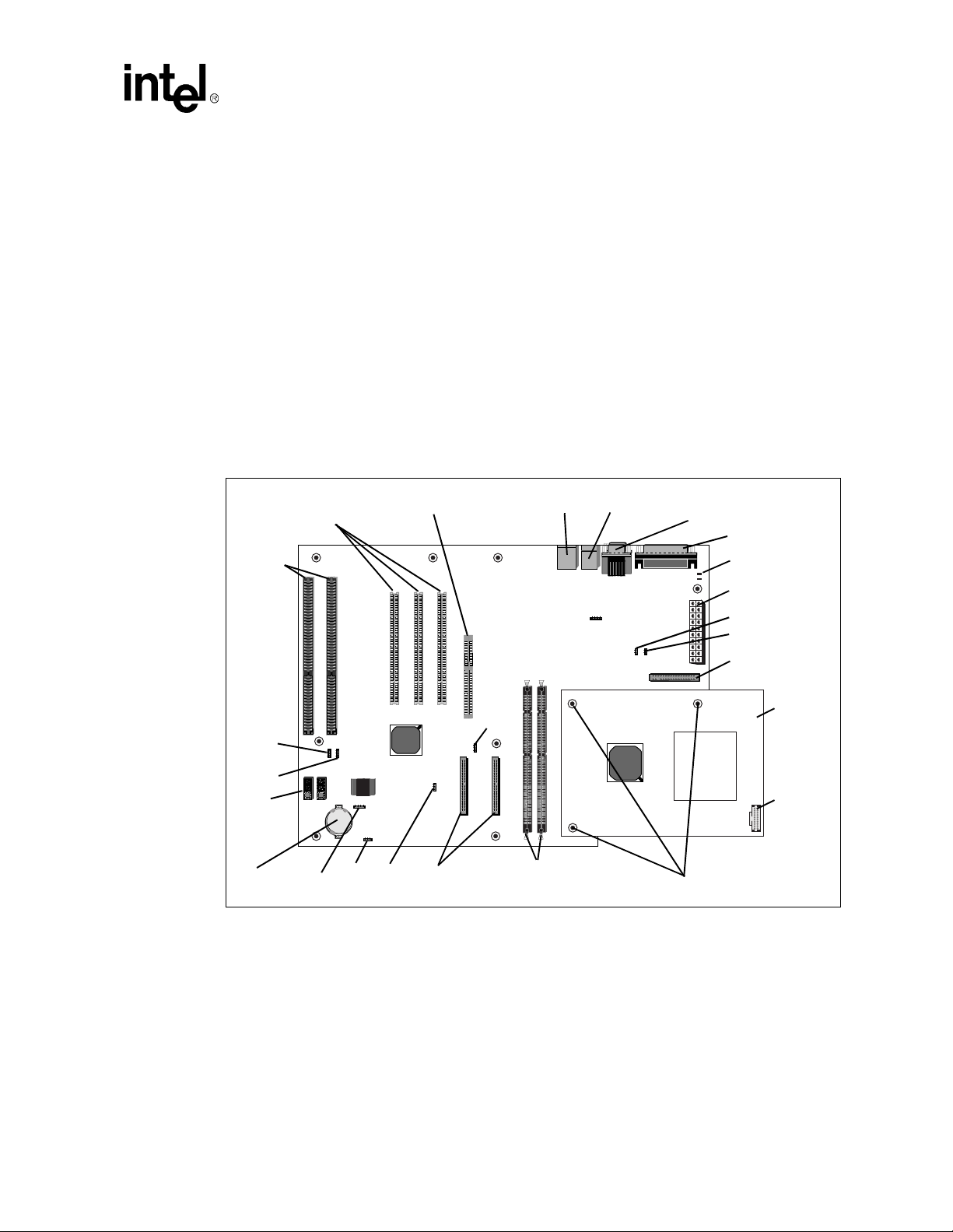
Figure 2-1. Evaluation Board Jumpers and Connectors
Connectors
ISA
Connectors
J21
J22
Post
Code
Debugger
Battery JP2
PCI AGP Connector USB Keyboard (Top) COM1 (Top)/
/Mouse COM2
J12
J5 J6
J12
J7 J8 J9
J2
J1
J12
J13
J18J17
J3
J4
J14 J15
JP1
D1
D2
J11
Parallel Port
LEDs
ATX Power
Connector
J14
J15
Floppy
Connector
J20
U12 U13
J21 J22
U11
JP2
J24
J23J24 SDRAM
IDE Connectors
J23
J20
JP2 JP3
IDE2 IDE1
DIMM Slots
Special Mounting Holes
Processor
Assembly
ITP
Debugger
Port
J2
Celeron™ Processor Development Kit Manual
2-5
Page 16

Getting Started
3. Make sure the board’s jumpers are set to the following default locations.
• J14 - Not installed
• J15 - Installed
• J20 - Jump er pins 2-3
• J21 - Jump er pins 2-3
• J22 - Jump er pins 2-3
• J23 - Jump er pins 2-3
• J24 - Jump er pins 1-2
4. Mount the hardware:
• Table-top operation: The evaluation board is shipped with standoff “feet” for use in a
table-top environment. These feet are installed on the evaluation board to raise it off the
table surface.Your kit contains two bags of mounting hardware. One bag contains eight
standoff feet, eight mounting screws, and eight washers. Another bag has three shorter
feet that must be attached slightly differently.
— To mount the eight standard feet, insert a washer onto a screw, then push the screw
through the top of the board. From below the board, thread one of the longer feet
onto the screw.
— To mount the three special feet, screw the three
screws. See Figure 2-1 for the location of the three special holes.
Warning: Do not remove the nuts from these three holes! This will detach the process or ass e mbly from the
baseboard, and Intel will no long er support the evaluation board.
• The evaluation board is not ATX compatible.
5. Connect desired storage devices to the evaluation board:
The evaluation board supports Primary and Secondary I DE interfaces that can each host one or
two devices (master/slave). When you are using multiple devices, such as a hard disk and a
CD-ROM drive, make sure the hard disk drive has a jumper in the master position and the CDROM has a jumper in the slave position. When you are using a single IDE device with the
evaluation board, be sure that the jumpers set correctly fo r sing le master operation. Fo r jumper
settings for other configurations, consult the drive’s documentation.
Note: The evaluation board BIOS only supports hard drives of 16 Gbytes or less.
• Installing the IDE hard disk drive included in your kit:
— Connect the hard drive’s IDE connector to the JP4 connector on the evaluation
board. Be sure to align Pin 1 of the cable connector with pin 1 of JP4.
— Connect the other end to the hard disk drive.
Caution: Make sure the tracer on the ribbon cable is aligned with pin 1 on both the hard disk and the IDE
connector header. Connecting the cable backwards can damage the evaluation board or the hard
disk.
shorter feet onto the existing
2-6
— Connect the hard drive to the power supply.
Note: The hard disk is already formatted and is pre-loaded with the QNX Real-Time Operating System
for Intel Architecture.
Celeron™ Processor Development Kit Manual
Page 17

Getting Started
— You may have to make changes to the system BIOS to enable this hard disk. See
Chapter 5, “BIOS Quick Reference” for more information.
• Floppy drive: A floppy disk drive connected to the evaluation board is the most direct
method for loading software.
— Insert floppy cable into JP1 (be sure to orient Pin 1 correctly).
— Connect the other end of the ribbon cable to the floppy drive.
— Connect a power cable to the floppy drive.
— You must make changes to the system BIOS to enable this floppy disk. See
Chapter 5, “BIOS Quick Reference” for more information.
6. Make sure the SDRAM DIMM is installed in the socket labeled J18.
7. Connect a PS/2 mouse and keyboard (see Figure 2-1 for connector locations).
Note: J1 (on the baseboard) is a stacked PS/2 connector. The bottom connector is for the mouse and the
top is for the keyboard.
8. Install the Chips and Technologies PCI video adapter into one of the available PCI slots.
Connect the monitor cable to the VGA port on the card.
9. Connect the power supply:
You’ll need a standard ATX PC power supply. Make sure the power supply is unplugged (or
turned off), then connect the power supply cable to the power header (J11).
Note: Some ATX power supplies do not have an on/off switch. In this case remove jumper J20 before
plugging in the ATX power connector. J20 controls an internal power supply on/off switch. When
you are ready to apply power , ins ert the ju mper on pins 2-3 . You may want to wire this header up to
a toggle switch for convenience.
Turn on the power to the monitor and evaluation board. When the power is on you should see two
power-indicator LEDs light up (located next to the ATX power connector in the upper right corner
of the board; see Figure 2-1). Check to see that the fan on the processor is operating.
2.6 Configuring the BIOS
General Software’s BIOS software is pre-loaded on the evaluation board. You will have to make
changes to the BIOS to enable hard disks, floppy disks and other supported features You can use
the Setup program to modify BIOS settings and control the special features of the system. Setup
options are configured through a menu-driven user interface. Chapter 5, “BIOS Quick Reference”
contains a description of BIOS options.
BIOS updates may periodically be posted to Intel’s Developers’ web site at
http://developer.intel.com/.
Celeron™ Processor Development Kit Manual
2-7
Page 18

Page 19
Theory of Operation
3.1 Block Diagram
Figure 3-1. Evaluation Board Block Diagram
3
Processor Assembly
ITP
VCCcore
Voltage
Regulator
Clock Generator
USB
I/O APIC
Boot
Flash
Celeron™ Processor
with 128 Kbyte
Integrated L2 Cache
PIIX4E
XD Bus
Processor
Side Bus
82443BX
Host Bridge/Controller
PCI Bus
ISA Bus
Thermal
Sensor
DRAM Bus
AGP Bus
Bus Master IDE
SMBus
72-Bit DIMM
AGP Connector
PCI Connectors
ISA Connectors
72-Bit DIMM
PS/2 Mouse
PS/2 Keyboard
Floppy Drive
SMC FDC37B78X
SuperI/O*
Celeron™ Processor Development Kit Manual
IEEE 1284 Parallel Port
COM1
COM2
3-1
Page 20

Theory of Operation
3.2 System Operation
The Celeron™ processor evaluation board is a full-featured system board and processor assembly.
The processor assembly includes either a 366-MHz or a 433-MHz Celeron processor (based on the
development kit purchased) with 128 Kbytes of integrated L2 cache and the Intel 82443 BX Host
Bridge/Controller. The evaluation board contains the Intel 82371EB PCI-to-ISA/IDE Xcelerator
(PIIX4E) and other system and I/O peripherals.
The evaluation board and pr oces sor assembly support 300-MHz, 366-MHz, and 433 MHz Cel eron
processors with 128 Kbytes of integrated L2 cache. The customer may remove the Celeron
processor from the processor socket and replace it with another supported version. Do not remove
the processor assembly. The evaluation board automatically detects which processor is installed in
the socket.
3.2.1 Celeron Processor
The Celeron processor for appli ed computing is of fered at 36 6 MHz and 433 MHz with a processo r
system bus speed of 66 MHz. The Celeron pr ocessor co nsists of a Pentium
an integrated second level cache and a 64-bit high-performance host bus. The processor has a
private second level cache bus that allows a high-performance 64-bit wide cache subsystem to be
integrated on the same die as the processor. The processor can cache up to 4 Gbytes of memory
using 128 Kbytes of L2 cache, 16 Kbytes of L1 data cache and 16 Kbytes of L2 code cache. The
private first and second level cache operate at the same frequency and voltage as the processor core
to improve performance and reduce total system power consumption.
3.2.2 82443BX Host Bridge/Controller
The Intel® 440BX AGPset supports the Pentium II processor architecture. It interfaces with the
Celeron processor system bus at 66 MHz. Along with its Host-to-PCI bridge interface, the
82443BX Host Bridge/Controller has been optimized with a 66MHz SDRAM memory controller
and data path unit. The 82443BX also features the Accelerated Graphi cs Port (AGP) interface. Th e
82443BX component includes the following functions and capabilities:
• 64-bit GTL+ based system data bus interface
• 32-bit system address bus support
• 64/72-bit main memory interface with optimized support for SDRAM
• 32-bit PCI bus interface with integrated PCI arbiter
• AGP interface with up to 133 MHz data transfer capability
• Extensive data buffering between all interfaces for high throughput and concurrent operations
®
II processor core with
3-2
Celeron™ Processor Development Kit Manual
Page 21

3.2.2.1 System Bus Interface
The 82443BX supports a maximum of 4 Gbytes of memory address space from the processor
perspective. The largest address size is 32 bits. The 82443BX provides bus control signals and
address paths for transfers between the processor bus, PCI bus, Accelerated Graphics Port and
main memory. The 82443BX supports a 4-deep-in-order queue, which provides support for
pipelining of up to four outstanding transaction requests on the system bus.
For system bus-to-PCI transfers, the addresses are either translated or directly forwarded on the
PCI bus, depending on the PCI address space being accessed. When the access is to a PCI
configuration space, the processor I/O cycle is mapped to a PCI configuration space cycle. When
the access is to a PCI I/O or memory space, the processor address is passed without modification to
the PCI bus. Certain memory address ranges are dedicated for a graphics memory address space.
When this space or a portion of it is mapped to main DRAM, the address is translated by the AGP
address remapping mech ani sm an d the request is forwarde d to t h e DRAM subsystem. A portion of
the graphics aperture can be mapped on the AGP, and the corresponding system bus cycles
accessing that range are forwarded to the AGP without any translation. The AGP address map
defines other system bus cycles that are forwarded to the AGP.
3.2.2.2 Accelerated Graphics Port (AGP) Interface
The 82443BX supports an AGP interface. The AGP interface has a maximum theoretical transfer
rate of ~532 Mbytes/s.
Theory of Operation
3.2.2.3 System Clocking
The 82443BX operates the system bus interface at 66 MHz, the PCI bus at 33 MHz and the AGP at
a transfer rate of 66/133 MHz. The 82443BX clocking scheme uses an external clock synthesizer
that produces reference clocks for the system bus and PCI interfaces. The 82443BX generates the
AGP and DRAM clock signals. Please refer to the CK97 Clock Synthesizer/Driver Specification
(order number 243867).
3.2.3 ITP
The evaluation board is pop ulated with a 2.5 V ITP debu gger port. The ITP por t provid es a path for
debugger tools like emulators, in-target probes, and logic analyzers to gain access to the Celeron
processor registers and signals without affecting high speed operation. This allows the system to
operate at full speed with the debugger attached.
Celeron™ Processor Development Kit Manual
3-3
Page 22

Theory of Operation
3.2.4 82371EB PCI to ISA/IDE Xcelerator (PIIX4E)
The 82443BX is designed to support the PIIX4E I/O bridge. The PIIX4E is a highly-integrated
multifunctional component that support s th e following:
• PCI Revision 2.1 compliant PCI-to-ISA bridge with support for 33 MHz PCI operations
• ACPI Power Management support
• Enhanced DMA controller, interrupt controller and timer functions
• Integrated IDE controller with Ultra DMA/33 support
• USB host interface with support for two USB ports
• System Management Bus (SMB) with support for DIMM Serial Presence Detect
3.2.5 DRAM
The evaluation board provides two 168-pin DIMM module connectors. The DRAM interface is a
64-bit data path that supports Synchronous DRAM (SDRAM). The DRAM interface supports
4 Mbytes to 256 Mbytes of 4-Mbit, 16-Mbit and 64-Mbit DRAM and SRAM technology (both
symmetrical and asymmetrical). Parity is not supported. One 32-Mbyte SDRAM DIMM is
included in the kit.
3.2.6 Power
The evaluation board uses an indus try standard ATX-style power supply with a 20- pin connect or . A
230-watt (minimum) supply is recommended. Note th at the ATX power connector is keyed to
prevent incorrect insertion. See “ATX Power Connector” on page 4-3 for a detailed description of
the power connector.
Make sure that the AT X power supply is not plugged into the wall when connecting or
disconnecting it from the evaluation board.
3.2.7 Boot ROM
The system boot ROM installed at U11 is a 2-Mbit 28F002BC flash device. The system is set up
for in-circuit reprogramming of the BIOS, but the flash device is also socketed. This device is
addressable on the XD bus extension of the ISA bus.
3.2.8 RTC/NVRAM
The RTC and NVRAM are contained within the 82371EB PIIX4E device. CMOS NVRAM
backup is provided by a 3-V lithium-ion battery.
3.2.9 Legacy I/O
Support for legacy I/O functions is provided by the Intel 82371EB PIIX4E and the SMC
FDC37B78X SuperI/O* device.
3-4
Celeron™ Processor Development Kit Manual
Page 23

3.2.10 IDE Support
The evaluation board supports both a primary and secondary IDE interface via two 40-pin IDE
connectors. The connector labeled IDE1 is the primary interface. IDE2 is the secondary interface.
3.2.11 Floppy Disk Support
Floppy disk support is provided by the SMC FDC37B78X SuperI/O device. One 34-pin floppy
connector is provided on the evaluation board.
3.2.12 Keyboard/Mouse
Keyboard and mouse support are provided by the SMC FDC37B8X SuperI/O device. The
keyboard and mouse connectors (J1) are PS/2 style, 6-pin stacked miniature DIN connectors. The
top connector is for the keyboard and the bottom connector is for the mouse.
3.2.13 USB
USB support is provided through the PIIX4E and can be used through connector J2.
Theory of Operation
3.2.14 RS232 Ports
Two serial I/O ports provided by the SMC FDC37B78X SuperI/O device. Two 9-pin RS232
connectors are provided on a single stacked connector (J4).
3.2.15 IEEE 1284 Parallel Port
One 25-pin IEEE 1284 parallel port connector controlled by the SMC FDC37B78X SuperI/O
device is provided (J3).
3.2.16 PCI Connectors
Three industry standard 32-bit, 5-V PCI connectors are provided on the evaluation board. The
connectors are designed to handle either a 5-V only card or a universal card. 3.3-V cards are not
supported.
3.2.17 ISA Connectors
Two 16-bit ISA connectors are provided on the evaluation board.
3.2.18 AGP Connector
AGP support is provided through the 82443BX Host Bridge/Controller. One industry standard
AGP connector (J13) is provided on the evaluation board.
Celeron™ Processor Development Kit Manual
3-5
Page 24
Theory of Operation
3.2.19 Post Code Debugger
The evaluation board has an on-board Post Code Debugger. Data from any program that does an
I/O write to 0080H is lat ched and di splayed o n the two LEDs (U12 and U1 3). During BIOS startup,
codes are posted to these LEDs to indicate what the BIOS is doing. Application programs can post
their own data to these LEDs by writing to I/O address 0080 H.
3.2.20 Clock Generation
There are three devices on the baseboard which generate and distribute the clocks used by the
entire system. These are the CY2280 clock synthesizer, CY2318NZ clock bu f fer and the CY23009
zero delay buffer. Not all of these devices are used on this version of the evaluation board.
The CY2280 generates the clocks for the Celeron processor, Host Bridge/Controller, cache, PCI,
USB and ISA bus. The processor clock runs at 66 MHz. The PCI clocks run at 33 MHz. This
device is capable of spread spectrum clocking. If spread spectrum clocking is enabled, a 0.5%
down spread will be introduced in the processor and PCI clocks.
The CY2318NZ clock buffer is used to buffer the clock signals sent to the SDRAM DIMMS. The
SDRAM interface operates at 66 MHz.
The CY2309 Zero Delay Buffer is not used by the evaluation board.
3.2.21 Interrupt Map
Table 3-1. Interrupts
IRQ System Resources
NMI I/O Channel Check
0 Reserved, Interval Timer
1 Reserved, Keyboard buffer full
2 Reserved, Cascade interrupt from slave PIC
3 Serial Port 2
4 Serial Port 1
5 Parallel Port (PNP0 option)
6 Floppy
7 Parallel Port 1
8 Real Time Clock
9 IRQ2 Redirect
10 Reserved. Not supported.
11 Reserved. Not supported.
12 Onboard Mouse Port if present, else user available
13 Reserved, Math coprocessor
14 Primary IDE if present, else user available
15 Reserved. Not supported.
3-6
Celeron™ Processor Development Kit Manual
Page 25
3.2.22 Memory Map
T able 3-2. Memory Map
Theory of Operation
Address Range
(Hex)
100000-8000000 127.25M Extended Memory
E0000-FFFFF 128K BIOS
C8000-DFFFF Available expansion BIOS area (Flash disk memory window)
A0000-C7FFF Off-board video memory and BIOS
9FC00-9FFFF 1K Extended BIOS Data (movable by QEMM, 386MAX)
80000-9FBFF 127K Extended conventional
00000-7FFFF 512K Conventional
Size Description
Celeron™ Processor Development Kit Manual
3-7
Page 26

Page 27

Hardware Reference
This section provides reference information on the system design. Included in this section is
connector pinout information, jumper settings, and other system design information.
4.1 Processor Assembly
The processor assembly cont ai ns t he Cel er on™ proces s or, the 82443BX Host Bridge/Controller, a
voltage regulator and an ITP debugger connector. The assembly connects to the baseboard via a
400-pin connector.
Warning: The processor assembly is attached to the baseboard at the factory. Do not remove the processor
assembly from the baseboard. Intel will not support the processor assembly or the baseboard if any
portion of the assembly is removed by the customer.
4.1.1 Thermal Management
The objective of thermal management is to ensure that the temperature of each component is
maintained within specified functional limits. The functional temperature limit is the range within
which the electrical circuits can be expected to meet their specified performance requirements.
Operation outside the functional limit can degrade system performance and cause reliability
problems.
4
Important: The evaluation kit contains a heatsink and fan attached to the top of the Celeron processor. This
thermal solution has been tested in an open air environment at room temperature and is sufficient
for evaluation purposes only. It is up to the designer to provide adequate thermal management for
any designs derived from the schematics provided in your kit.
4.1.2 ITP Debugger Port
The evaluation platform i s p opu l ated wit h a 2.5 V ITP debugger port . T he I T P po rt pro vi des a path
for debugger tools like emulators, in-target probes, and logic analyzers to gain access to the
Celeron processor’s registers and signals without affecting high speed operation. This allows the
system to operate at full speed with the debugger attached.
4.2 Post Code Debugger
The evaluation board has an on-board Post Code Debugger. Data from any code that does an I/O
write to 80H is latched on the two led di splays (U12/U13). During BIOS startup, code is posted to
these LEDs to indicate what the BIOS is doing. Application code can post its own data to these
LEDs by doing an I/O write to address 80H. The 22V10 PLD code used to implement this function
is included in Appendix A, “PLD Code Listing.”
Celeron™ Processor Development Kit Manual
4-1
Page 28
Hardware Reference
4.3 ISA and PCI Expansion Slots
The evaluation platform has three PCI expansion slots and two ISA slots.
4.4 PCI Device Mapping
On the evaluation platform the PCI devices are mapped to PCI device numbers by connecting an
address line to the IDSEL signal of each PCI device. Table 4-1 s hows the mapping of PCI devices.
Table 4-1. PCI Device Mapping
Device Address Line PCI Device Number
PIIX4E AD18 7
PCI Slot 0 (J7) AD28 17
PCI Slot 1 (J8) AD29 18
PCI Slot 2 (J9) AD30 19
4-2
Celeron™ Processor Development Kit Manual
Page 29
4.5 Connector Pinouts
4.5.1 ATX Power Connector
Table 4-2 shows the signals assigned to the ATX style power connector.
Table 4-2. Primary Power Connector (J11)
Pin Name Function
1 3.3 V 3.3 V
2 3.3 V 3.3 V
3 GND Ground
4 +5V +5 V VCC
5 GND Ground
6 +5V +5 V VCC
7 GND Ground
8 PWRGD Power Good
9 5VSB Standby 5 V
10 +12 V +12 V
11 3.3 V 3.3 V
12 –12 V –12 V
13 GND Ground
14 PS_ON# Soft-off control
15 GND Ground
16 GND Ground
17 GND Ground
18 –5 V –5 Volts
19 +5 V +5 V VCC
20 +5 V +5 V VCC
Hardware Reference
Celeron™ Processor Development Kit Manual
4-3
Page 30
Hardware Reference
4.5.2 ITP Debugger Connector
Table 4-3. ITP Connector Pin Assignment (J2 on the Processor Assembly)
Pin Signal Pin Signal
1 RESET# 16 PREQ0#
2 GND 17 GND
3 DBRESET# 18 PRDY0#
4 GND 19 GND
5 TCK 20 PREQ1#
6 GND 21 GND
7 TMS 22 PRDY1#
8 TDI 23 GND
9 POWERON 24 PREQ2#
10 TDO 25 GND
11 DBINST# 26 PRDY2#
12 TRST# 27 GND
13 GND 28 PREQ3#
14 BSEN# 29 BCLK
15 GND 30 PRDY3#
4.5.3 Stacked USB
P0 is the bottom connector. P1 is on top.
Table 4-4. USB Connector Pinout (J2)
Pin P0 Signals P1 Signals
1 VCC0 VCC1
2 D0- D13 D0+ D1+
4 GND0 GND1
4-4
Celeron™ Processor Development Kit Manual
Page 31

4.5.4 Mouse and Keyboard Connectors
The keyboard port is on top. The mouse port is on the bottom.
Table 4-5. Keyboard and Mouse Connector Pinouts (J1 on the Baseboard)
Pin Signal Name
1Data
2 No Connect
3 Ground
4 +5 V (fused)
5Clock
6 No Connect
4.5.5 Parallel Port
Table 4-6. DB25 Parallel Port Connector Pinout (J3)
Hardware Reference
Pin
1 Strobe# 14 Auto Feed#
2 Data Bit 0 15 Fault#
3 Data Bit 1 16 INIT#
4 Data Bit 2 17 SLCT IN#
5 Data Bit 3 18 Ground
6 Data Bit 4 19 Ground
7 Data Bit 5 20 Ground
8 Data Bit 6 21 Ground
9 Data Bit 7 22 Ground
10 ACK# 23 Ground
11 Busy 24 Ground
12 Paper end 25 Ground
13 SLCT
Signal
Name
Pin
Signal
Name
Celeron™ Processor Development Kit Manual
4-5
Page 32

Hardware Reference
4.5.6 Serial Ports
COM1 is the top connector. COM2 is the bottom connector.
Table 4-7. Serial Port Connector Pinout (J4)
Pin Signal Name
1 DCD
2 Serial In (SIN)
3 Serial Out (SOUT)
4DTR
5GND
6DSR
7RTS
8CTS
9RI
4.5.7 IDE Connector
Table 4-8. PCI IDE1 (JP3) and IDE2 (JP4) Connector
Pin Signal Name Pin Signal Name
1 Reset IDE 2 Ground
3 Host Data 7 4 Host Data 8
5 Host Data 6 6 Host Data 9
7 Host Data 5 8 Host Data 10
9 Host Data 4 10 Host Data 11
11 Host Data 3 12 Host Data 12
13 Host Data 2 14 Host Data 13
15 Host Data 1 16 Host Data 14
17 Host Data 0 18 Host Data 15
19 Ground 20 Key
21 DRQ3 22 Ground
23 I/O Write# 24 Ground
25 I/O Read# 26 Ground
27 IOCHRDY 28 BALE
29 DACK 3# 30 Ground
31 IRQ14 32 IOCS16#
33 Addr 1 34 Ground
35 Addr 0 36 Addr 2
37 Chip Select 0# 38 Chip Select 1#
39 Activity 40 Ground
4-6
Celeron™ Processor Development Kit Manual
Page 33

4.5.8 Floppy Drive Connector
Table 4-9. Diskette Drive Header Connector (JP1)
Pin Signal Name Pin Signal Name
1 Ground 2 FDHDIN
3 Ground 4 Reserved
5 Key 6 FDEDIN
7 Ground 8 Index
9 Ground 10 Motor Enable A#
11 Ground 12 Drive Select B#
13 Ground 14 Drive Select A#
15 Ground 16 Motor Enable B#
17 Ground 18 DIR#
19 Ground 20 STEP#
21 Ground 22 Write Data#
23 Ground 24 Write Gate#
25 Ground 26 Track 00#
27 Ground 28 Write Protect#
29 Ground 30 Read Data#
31 Ground 32 Side 1 Select#
33 Ground 34 Diskette Change#
Hardware Reference
Celeron™ Processor Development Kit Manual
4-7
Page 34

Hardware Reference
4.5.9 PCI Slot Connector
Table 4-10. PCI Slots (J7, J8, J9)
Pin Signal Name Pin Signal Name Pin Signal Name Pin Signal Name
A1 VC C B1 - 12V A32 AD16 B32 AD17
A2 + 12V B2 GND A33 3.3V B33 CBE2#
A3 VCC B3 GND A34 FRAME# B34 GND
A4 VC C B4 No Connect A35 GND B35 IRDY#
A5 VCC B5 VCC A36 TRDY# B36 3.3 V
A6 PIRQ1# B6 VCC A37 GND B37 DEVSEL#
A7 PI RQ 3# B7 PIRQ2# A38 STOP# B38 GND
A8 VCC B8 PIRQ0 A39 3.3 V B39 LOCK#
A9 No Connect B9 PRSNT1B# A40 SDONE B40 PERR#
A10 VCC B10 No Connect A41 SBO# B41 3.3 V
A11 No Connect B11 PRSNT2B# A42 GND B42 SERR#
A12 GND B12 GND A43 PAR B43 3.3V
A13 GND B13 GND A44 AD15 B44 CBE1#
A14 No Connect B14 No Connect A45 3.3V B45 AD14
A15 RST# B15 GND A46 AD13 B46 GND
A16 VCC B16 PCLK3 A47 AD11 B47 AD12
A17 GNT1# B17 GND A48 GND B48 AD10
A18 GND B18 REQ# A49 AD9 B49 GND
A19 Reserved B19 VCC A50 KEY B50 KEY
A20 AD30 B20 AD31 A51 KEY B51 KEY
A21 3.3V B21 AD29 A52 CBEO# B52 AD8
A22 AD28 B22 GND A53 3.3 V B53 AD7
A23 AD26 B23 AD27 A54 AD6 B54 3.3 V
A24 GND B24 AD25 A55 AD4 B55 AD5
A25 AD24 B25 3.3 V A56 GND B56 AD3
A26 IDSEL B26 CBE3# A57 AD2 B57 GND
A27 3.3V B27 AD23 A58 AD0 B58 AD1
A28 AD22 B28 GND A59 VCC B59 VCC
A29 AD20 B29 AD21 A60 REQ64# B60 ACK64#
A30 GND B30 AD19 A61 VCC B61 VCC
A31 AD18 B31 3.3 V A62 VCC B62 VCC
4-8
Celeron™ Processor Development Kit Manual
Page 35

4.5.10 ISA Slot Connector
Table 4-11. ISA Slots (J5, J6)
Pin Signal Name Pin Signal Name Pin Signal Name Pin Signal Name
A1 IOCHK# B1 GND A26 SA5 B26 DACK2#
A2 SD7 B2 RSTSLOT A27 SA4 B27 TC
A3 SD6 B3 VCC A28 SA3 B28 BALE
A4 SD5 B4 IRQB9 A29 SA2 B29 VCC
A5 SD4 B5
A6 SD3 B6 DREQ2 A31 SA0 B31 GND
A7 SD2 B7
A8 SD1 B8 ZEROWS# C2 LA23 D2 IOCS16#
A9 SD0 B9 +12V C3 LA22 D3 IRQB10
A10 IOCHRDY B10 GND C4 LA21 D4 IRQB11
A11 AEN B11 SMEMW# C5 LA20 D5 IRQ B11
A12 SA19 B12 SMEMR# C6 LA19 D6 IRQ15
A13 SA18 B13 IOW# C7 LA18 D7 IRQ14
A14 SA17 B14 IOR# C8 LA17 D8 DACK0
A15 SA16 B15 DACK3# C9 MEMR# D9 DREQ0
A16 SA15 B16 DREQ3 C10 MEMW# D10 DACK5
A17 SA14 B17 DACK1# C11 SD8 D11 DREQ5
A18 SA13 B18 DREQ1 C12 SD9 D12 DACK6#
A19 SA12 B19 REFRESH# C13 SD10 D13 DREQ6
A20 SA11 B20 SYSCLK C14 SD11 D14 DACK7#
A21 SA10 B21 IRQA7 C15 SD12 D15 DREQ7#
A22 SA9 B22 IRQA6 C16 SD13 D16 VCC
A23 SA8 B23 IRQA5 C17 SD14 D17 MASTER#
A24 SA7 B24 IRQA4 C18 SD15 D18 GND
A25 SA6 B25 IRQA3
Hardware Reference
–5V A30 SA1 B30 OSC
–12V C1 SBHE# D1 MEMCS16#
Celeron™ Processor Development Kit Manual
4-9
Page 36
Hardware Reference
4.6 AGP Connector
Table 4-12. AGP Slot (J13)
Pin#BAPin#BA
1 OVRCNT# 12V 34 Vddq3.3 Vddq3.3
2 5.0V TYPEDET# 35 AD21 AD22
3 5.0V Reserved 36 AD19 AD20
4 USB+ USB- 37 GND GND
5 GND GND 38 AD17 AD18
6 INTB# INTA# 39 C/BE2# AD16
7 CLK RST# 40 Vddq3.3 Vddq3.3
8 REQ# GNT# 41 IRDY# FRAME#
9 VCC3.3 VCC3.3 42 3.3Vaux Reserved
10 ST0 ST1 43 GND GND
11 ST2 Reserved 44 Reserved Reserved
12 RBF# PIPE# 45 VCC3.3 VCC3.3
13 GND GND 46 DEVSEL# TRDY#
14 Reserved Reserved 47 V ddq3.3 STOP#
15 SBA0 SBA1 48 PERR# PME#
16 VCC3.3 VCC3.3 49 GND GND
17 SBA2 SBA3 50 SERR# PAR
18 SB_STB Reserved 51 C/BE1# AD15
19 GND GND 52 Vddq3.3 Vddq3.3
20 SBA4 SBA5 53 AD14 AD13
21 SBA6 SBA7 54 AD12 AD11
22 KEY KEY 55 GND GND
23 KEY KEY 56 AD10 AD9
24 KEY KEY 57 AD8 C/BE0#
25 KEY KEY 58 Vddq3.3 Vddq3.3
26 AD31 AD30 59 AD_STB0 Reserved
27 AD29 AD28 60 AD7 AD6
28 VCC3.3 VCC3.3 61 GND GND
29 AD27 AD26 62 AD5 AD4
30 AD25 AD24 63 AD3 AD2
31 GND GND 64 Vddq3.3 Vddq3.3
32 AD_STB1 Reserved 65 AD1 AD0
33 AD23 C/BE3# 66 Reserved Reserved
NOTES:
1. Reserved pins are only for future use by the AGP interface specification.
2. IDSEL# is not a pin on the AGP connector. AGP graphics components should connect the AD16 signal to
the 3. 3 volt IDSEL# function internal to the component.
3. All 3.3 volt cards leave the TYPEDET signal open. All 1.5 volt cards tie this signal hard to ground.
4-10
Celeron™ Processor Development Kit Manual
Page 37
4.7 Jumpers
T a bl e 4-13 shows defau l t Ju mper set t i ngs.
Table 4-13. Default Jumper Settings
Jumper Function Settings
J14 Enable Spread Spectrum Clocking
J15 Clock Frequency Selection
J20 On/Off
J21 Flash BIOS VPP Select
J22 Flash BIOS boot block control
J23 SMI# Source
J24 CMOS RAM Clear
Hardware Reference
In – Enable Spread Spectrum
Out – Disable Spread Spectrum (Default)
In – 66 MHz Processor Clock (Default)
Out – Reserved
1–2 Reserved
2–3 On (Default)
No Jumper Installed – Off
1–2 12 V
2–3 5 V (Default)
1–2 12 V
2–3 5 V (Default)
1–2 SMI# controlled by IOAPIC
2–3 SMI# controlled by PIIX4E (Default)
1–2 Normal Operation (Default)
2–3 Clear CMOS RAM
4.7.1 Enable Spread Spectrum Clocking (J14)
This jumper is used to enable or disable spread spectrum clocking on the clock synthesizer. When
this jumper is in, a 0.5% down spread will be introduced into the PCI and processor clocks. The
default setting is no jumper installed, which di sables spread spectrum clocking.
4.7.2 Clock Frequency Selection (J15)
This jumper controls the frequency of the processor clock. When the jumper is in, 66 MHz
operation is supported. This is the only setting supported by this evaluation k it.
Caution: Leave this jumper installed. When the jumper is out, 100 MHz processor clocks will be generated.
This position is not supported and may cause damage to the processor.
4.7.3 On/Off (J20)
This jumper is used to control the state of the ATX power supply. When this jumper is removed, the
power supply will be turned off. Placing the jumper in the 2-3 position will turn the power supply
on.
The 1-2 position is reserved and should not be used.
Celeron™ Processor Development Kit Manual
4-11
Page 38

Hardware Reference
4.7.4 Flash BIOS VPP Select (J21)
This jumper controls the voltage presented to the flash BIOS VPP pin. The 2-3 position supplies
5 V and is the default for normal o perati on. T his pos iti on in hibit s pr ogramming or erasing the f lash
BIOS.
The 1-2 position supplies 12 V and should only be used if directed to do so by a utility that is used
to reprogram the BIOS.
4.7.5 Flash BIOS Boot Block Control (J22)
This jumper controls the Boot Block protection of the flash BIOS. When this jumper is in the 2-3
position, the boot block is locked and cannot be programmed. This is the default position of this
jumper.
The 1-2 position unlocks the boot block so that it can be erased and reprogrammed. This position
should only be used under the direction of a utility that is designed to reprogram the boot block of
the flash device.
4.7.6 SMI# Source Control (J23)
This jumper selects the source of the SMI# interrupt to the processor. Only the 2-3 position which
selects the PIIX4E is supported. The 1-2 position is res erved for future use.
4.7.7 CMOS RAM Clear (J24)
This jumper controls power to the battery backed-up CMOS RAM. This RAM is used to sto r e
information about the system configuration that is required by the BIOS. The 1-2 position is for
normal operation. The 2-3 position allows for the RAM to be cleared.
To clear the RAM perform the following steps:
1. Remove power from the evaluation platform by removing jumper J20
2. Move J24 to the 2-3.
3. Disconnect the power supply (J11).
4. Install J24 in the 1- 2 position.
5. Reconnect the power supply (J11).
6. Reboot the system and enter the BIOS setup screen to configure the system.
4.7.8 Push Button Switches
There are two push button switches on the evaluation board labeled S1 and S2.
• S1 is non-functional and reserved for future use.
• S2 is the reset button. Press S2 to force a hardware reset of the system.
4-12
Celeron™ Processor Development Kit Manual
Page 39

4.8 In-Circuit BIOS Update
The BIOS can be upgraded in-circuit. BIOS updates may periodically be posted to Intel’s
Developers’ site at http://www.intel.com/design/.
To r eprogram the BIOS:
1. Set Jumper J21 and Jumper J22 to the 1-2 position on the evaluation platform.
2. Download the new BIOS upgrade file from Intel’s Developers’ web site.
3. Extract the BIOS upgrade zip file onto a bootable floppy.
4. Insert the floppy disk into the floppy drive attached to the evaluation board.
5. Reboot the evaluation board so that it boots from the floppy.
6. Follow the on-screen instructions.
7. When the BIOS update program is finished, power down the board and reset the jumpers at
J21 and J22 to the 2-3 position.
Hardware Reference
Celeron™ Processor Development Kit Manual
4-13
Page 40

Page 41

BIOS Quick Reference
5
The Celeron processor evaluation board is licensed with a single copy of Embedded BIOS and
Embedded DOS software from General Software, Inc.
demonstration purposes only and must be licensed directly from General Software, Inc. for
integration with new designs. General Software may be reached at (800) 850-5755, on the web at
http://www.gensw.com, or via email at sales@gensw.com.
BIOS updates may periodically be posted to the Intel Developers’ web site at
http://developer.intel.com/.
5.1 BIOS and Pre-Boot Features
The system’s pre-boot environment is managed with an adaptation of Embedded BIOS from
General Software. The pre-boot environment includes POST, Setup Screen System, Manufacturing
Mode, Console Redirection, Windows CE Loader (CE Ready), and Integrated BIOS Debugger. A
REFLASH tool is also available to update the BIOS image with new builds of Embedded BIOS
that may be obtained from General Software.
Before using the system, please read the following to properly configure CMOS settings, and learn
how to use the embedded features of the pre-boot firmware, Embedded BIOS.
The last two sections of this chapter provide the BIOS POST Codes and Beep codes.
5.2 Power-On Self-Test (POST)
1
This software is provided for
When the system is powered on, Embedded BIOS tests and initializes the hardware and programs
the chipset and other peri phera l comp onents. During this time, P OST p rogress codes are wri tten by
the system BIOS to I/O port 80H, allowing the user to monitor the progress with a special monitor.
“Embedded BIOS POST Codes” on page 5-12 lists the POST codes and their meanings.
During early POST, no video is available to display error messages should a critical error be
encountered; therefore, POST uses beeps on the speaker to indicate the failure of a critical system
component during this time. Consult “Embedded BIOS Beep Codes” on page 5-15 for a list of
Beep codes used by the system’s BIOS.
POST displays its progress on the system video device, which may be the video screen if a VGA
card is used, or on a terminal emulation program’s screen if output is redirected over a serial port.
1. General Software™, the GS Logo, Embedded BIOS™, BIOStart™, CE-Ready™, and Embedded DOS™ are trademarks or registered
trademarks of General Software, Inc.
Celeron™ Processor Development Kit Manual
5-1
Page 42

BIOS Quick Reference
Figure 5-1. BIOS POST Pre-Boot Environment
When the system is powered on for the first time, you’ll need to configure the system through the
Setup Screen System (described later) before peripherals, such as disk dr ives, are recognized by the
BIOS. The information is written to battery-backed CMOS RAM on the board’s Real Time Clock.
Should the board’s battery fail, this information will be lost and the board will need to be
reconfigured.
OEMs can modify the look-and-feel of POST with the Embedded BIOS adaptation kit. While the
demonstration BIOS looks and feels like a desktop PC, it is possible to eliminate messages, sounds,
delays, to make the POST effectively invisible.
5-2
Celeron™ Processor Development Kit Manual
Page 43

5.3 Setup Screen System
The system is configured from within the Setup Screen System, which is a series of menus that can
be invoked from POST by pressing the <DEL> key if the main keyboard is being used, or by
pressing ^C if the console is being redirected to a terminal program.
Figure 5-2. Embedded BIOS Setup Screen Menu
BIOS Quick Reference
Once in the Setup Screen System (Figure 5-2), the user can navigate with the UP and DOWN
arrow keys from the main conso le, or us e the ^E and ^X keys from the remote te rminal pro gram to
accomplish the same thing. TAB and ENTER are used to advance to the next field, and ‘+’ and ‘-’
keys cycle through values, such as those in the Basic Setup Screen, or the Diagnostics Setup
Screen.
5.3.1 Basic CMOS Configuration Screen
The system’s drive types, boot activities, and POST optimizations are configured from the Basic
Setup Screen (Figure 5-3). In order to use disk drives with your system, you must select
appropriate assignments of drive types in the left-hand column. Then, if you are using true floppy
and IDE drives (not memory disks that emulate these drives), you need to configu re the drive types
themselves in the Floppy Drive Types and IDE Drive Geometry sections. Finally, you’ll need to
configure the boot sequence in the middle of the screen. Once these selections have been made,
your system is ready to use.
Celeron™ Processor Development Kit Manual
5-3
Page 44

BIOS Quick Reference
Figure 5-3. Embedded BIOS Basic Setup Screen
5.3.2 Configuring Drive Assignments
Embedded BIOS allows the user to map a different file system to each drive letter. The BIOS
allows file systems for each floppy (Floppy0 and Floppy1), each IDE drive (Ide0, Ide1, Ide2, and
Ide3), and memory disks when configured (Flash0, ROM0, R AM0, etc. ) Figur e 5-3 shows how the
first floppy drive (Floppy0) is assigned to drive A: in the sy stem , and then how the first IDE drive
(Ide0) is assigned to drive C: in the system.
To switch two floppy disks around or two hard disks around, just map Floppy0 to B: and Floppy1
to A:, and for hard disks map Ide0 to D: and Ide1 to C:.
Caution: Take care to not skip drive A: when making floppy disk assignments, as well as drive C: when
making hard disk assignments . The first floppy should be A:, and the fir st hard dri ve s hou ld be C: .
Also, do not assig n th e s ame file system to more t h an one drive letter. Thus, Floppy0 should not be
used for both A: and B:. The BIOS permits this to allow embedded dev ices to alias drives, but
desktop operating systems may not be able to maintain cache coherency with such a mapping in
place.
A special field in this section entitled “Bo ot Method: (Windows CE/Boot Sector)” is used to
configure the CE Ready feature of the BIOS. For normal bo oting (DOS, Windows NT, etc.), select
“Boot Sector” or “Unused”.
5.3.2.1 Configuring Floppy Drive Types
If true floppy drive file systems (and not their emulators, such as ROM, RAM, or flash disks) are
mapped to drive letters, then the floppy drives themselves must be configured in this section.
Floppy0 refers to the first floppy disk drive on the drive ribbon cable (normally drive A:), and
Floppy1 refers to the second drive (drive B:).
5-4
Celeron™ Processor Development Kit Manual
Page 45

5.3.3 Configuring IDE Drive Types
If true IDE disk file systems (and not their emulators, such as ROM, RAM, or flash disks) are
mapped to drive letters, then the IDE drives themselves must be configured in this section. The
following table shows the drive assignments for Ide0-Ide3:
Table 5-1. IDE0-IDE3 Drive Assignments
File System Name Controller Mas ter/Slave
Ide0 Primary (1f0h) Master
Ide1 Primary (1f0h) Slave
Ide2 Secondary (170h) Master
Ide3 Secondary (170h) Slave
To use the primary master IDE drive in your system (the typical case), just configure Ide0 in this
section, and map Ide0 to drive C: in the Configuring Drive Assignmen ts section.
The IDE Drive Types section lets you select the type for each of the four IDE drives: None, User,
Physical, LBA, or CHS.
User This type allows the user to select the maximum cylinders, heads, and sectors
per track associated with the IDE drive. This method is now rarely used since
LBA is now in common use.
BIOS Quick Reference
Physical This type instructs the BIOS to query the drive’s geometry from the controller
on each POST. No translation on the drive’s geometry is performed, so this type
is limited to drives of 512 Mbytes or less. Com monly, this is used with
embedded ATA PC Cards.
LBA This type instructs the BIOS to query the drive’s geometry from the controller
on each POST, but then translate the geometry according to the industrystandard LBA convent ion. This support s up to 16-Gbyt e drives. Use this method
for all new drive s.
CHS This type instructs the BIOS to query the drive’s geometry from the controller
on each POST, but then translate the geometry according to the Phoenix CHS
convention. Using this type on a drive previously formatted with LBA or
Physical geometry might show data as being missing or corrupted.
Celeron™ Processor Development Kit Manual
5-5
Page 46

BIOS Quick Reference
5.4 Configuring Boot Actions
Embedded BIOS supports up to six different user-defined steps in the boot sequence. When the
entire system has been initialized, POST executes these steps in order until an operating system
successfully loads. In addition, other pre-boot features can be run before, after, or between
operating system load attempts. The following actions can be used:
Drive A: - K: Boot operating system from specified drive. If “Loader” is set to “BootRecord”
or “Unused”, then the standard boot record will be invoked, caus ing DOS,
Windows95/98, Windows NT, or other industry-standard operating systems to
load. If “Boot Method” is set to “Windows CE”, then the boot drive’s boot
record will not be used, and instead the BIOS will attempt to load and execute
the Windows CE Kernel file, NK.BIN, from the root directory of each boot
device.
Debugger Launch the Integrated BIOS Debugger. To return to the boot process from the
debugger environment, type “G” at the debugger prompt and press ENTER.
MFGMODE Initiate Manufacturing Mode, allowing the system to be configured remotely
via an RS232 connect to a host computer.
WindowsCE Execute a ROM-resident copy of Windows CE, if available. This feature is not
applicable unless properly configured by the OEM in the BIOS adaptation.
DOS in ROM Execute a ROM-resident copy of DOS, if available. This feature is not
applicable unless an XIP copy of DOS, such as Embe dded DOS-ROM, has been
stored in the BIOS boot ROM. Copies of Embe dded DOS-R OM may be
obtained from General Software.
None No action; POST proceeds to the next activity in the sequence.
5.5 Custom Configuration Setup Screen
The system’s hardware-specific features are configured with the Custom Setup Screen
(Figure 5-4). All features are straightforward except for the Redirect Debugger I/O option, which is
an extra embedded feature that allows the user to select whether the Integrated BIOS Debugger
should use standard keyboar d and video or RS 232 consol e redirect ion for in teracti on with the user.
If no video is available, the debugger is always redirected.
5-6
Celeron™ Processor Development Kit Manual
Page 47

Figure 5-4. Embedded BIOS Custom Setup Screen
5.6 Shadow Configuration Setup Screen
BIOS Quick Reference
The system’s Shadow Configuration Setup Screen (Figure 5-5) allows the selective enabling and
disabling of shadowing in 16 Kbyte sections, except for the top 64 Kbytes of the BIOS ROM,
which is shadowed as a unit. Normally, shadowing should be enabled at C000/C400 (to enhance
VGA ROM BIOS performance), and then E000-F000 should be shadowed to maximize system
ROM BIOS performance.
Figure 5-5. Embedded BIOS Shadow Setup Screen
Celeron™ Processor Development Kit Manual
5-7
Page 48

BIOS Quick Reference
5.7 Standard Diagnostics Routines Setup Screen
Embedded systems may require automated burn-in testing in the development cycle. This facility is
provided directly in the system’s system BIOS through the Standard Diagnostics Routines Setup
Screen (Figure 5-6). To use the system, selectively enable or disable features to be tested, and then
enable the “T ests Begin on ESC?” option to cause the system test suite to be invoked. To repeat the
system test battery continuously, you should also enable the “Continuous Testing” option. When
continuous testing is started, the system will continue until an error is encountered.
Caution: The disk I/O diagnostics perform write operations on those drives; therefore, only spare drives
should be used which do not contain data that could be harmed by the test.
Caution: The keyboard test may fail when in fact the hardware is operating within reasonable limits. This is
because although the device may produce occasional errors, the BIOS retries operations when
failures occur during normal operation of the system.
Figure 5-6. Standard Diagnostic Routines Setup Screen
5.8 Start System BIOS Debugger Setup Screen
The Embedded BIOS Integrated Debugger may be invoked from the Setup Screen main menu, as
well as a boot activity. Once invoked, the debugger will display the debugger prompt:
EB42DBG:
and await debugger commands. To resume back to the Setup Screen main menu, type the followi ng
command, which instructs the debugger to “go”:
EB42DBG: G
5-8
<ENTER>
Celeron™ Processor Development Kit Manual
Page 49
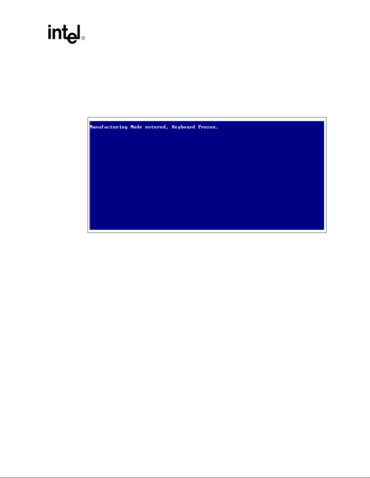
BIOS Quick Reference
5.9 Start RS232 Manufacturing Link Setup Screen
The Embedded BIOS Manufacturing Mode may be invoked from the Setup Screen main menu, as
well as a boot activity. Once invoked, Manufacturing Mode takes over the system and freezes the
console of the system (Figure 5-7). The host can resume operation of the system and give control
back to the system Setup Screen system with special control software.
Figure 5-7. Start RS232 Manufacturing Link Setup Screen
5.10 Manufacturing Mode
The system’s BIOS provides a special mode, called Manufacturing Mode, that allows the target to
be controlled by a host computer such as a laptop or desktop PC. Running special software
supplied by General Software, the host can access the target’s drives and manage the file systems
on the target, reprogram flash memories, and test target hardware.
A full discussion of the uses of Manufacturi ng Mo de i s beyond the scope of t his chap t er. Complete
documentation and host-side software is available directly from General Software. For more
information, visit the General Software web site at http://www.gensw.com .
5.10.1 Console Redirection
The system can operate either with a standard PC/A T or PS/2 keyboard and VGA video monitor , or
with a special emulation of a console over an RS232 cable connected to a host computer running a
terminal program. To see an example session with HYPERTERMINAL, see the d ebugger section’s
screen display (Figure 5-9).
To use the Console Redirection feature, simply remove the video display card from the system so
that no video ROM is available for the BIOS to detect. In the absence of any video support, the
BIOS automatically switches its keyboard and screen functions to serial I/O over COM1 on the
board. The hardware connection to the host computer requires a null modem cable.
Celeron™ Processor Development Kit Manual
5-9
Page 50
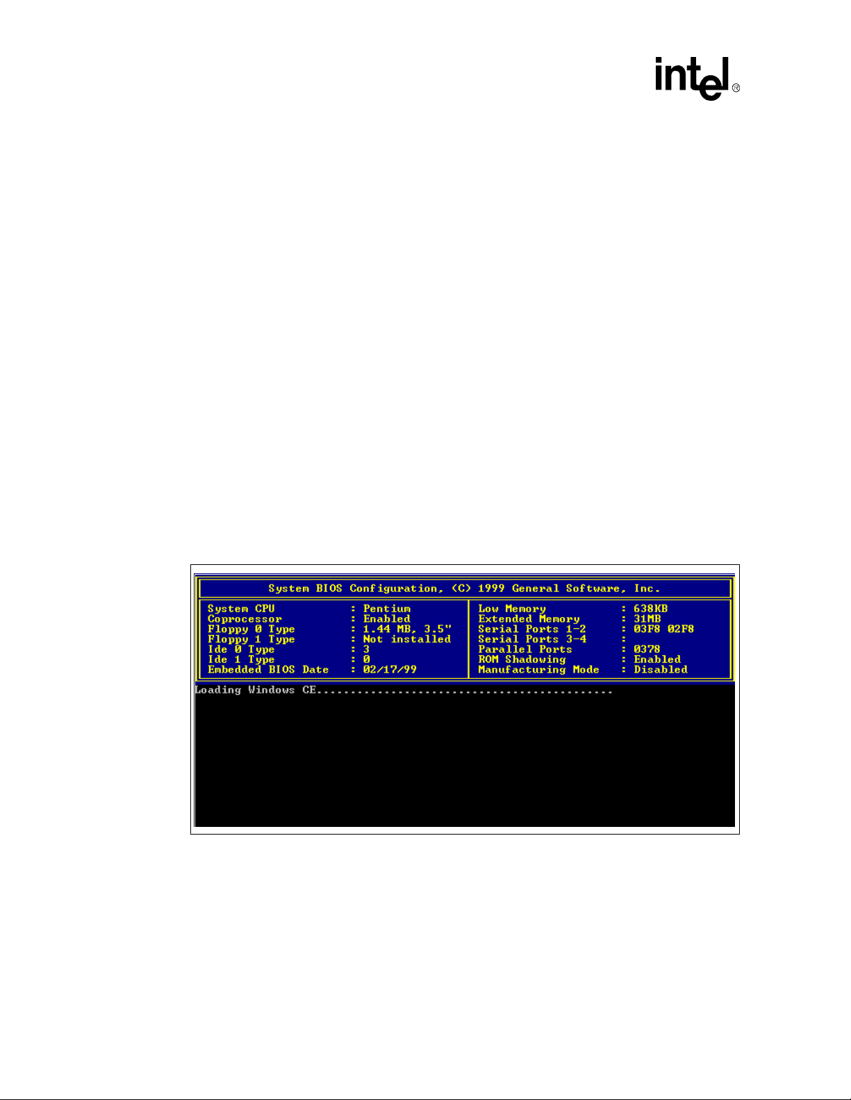
BIOS Quick Reference
The software on the target can be any terminal emulation program that supports ANSI terminal
mode, using 9600 baud, no parity, and one stop bit (Note: This can be modified by the OEM during
BIOS adaptation.) The program must be set to not use flow control, or the console may seem to
stall or not accept input.
Caution: HYPERTERMINAL’s default setting is to use flow control, which will render the console
inoperative. To change this, create a new session, change the flow control setting to “none”, save
the session, and exit HYPERTERMINAL. Then reinvoke HYPERTERMINAL with the session
and it will operate with the new flow control setting.
5.10.2 CE-Ready Windows CE Loader
Your system’s BIOS is “CE-Ready” and can directly boot Windows CE* without loading an
intermediate operating system such as DOS and LOADCEPC. Instead, the NK.BIN file can be
placed on a disk drive or drive emulator, and then the BIOS can be configured through the Basic
CMOS Configuration Setup Screen to boot the NK.BIN file from the boot drives instead of the
boot records on those driv es.
To configure your system to boot Windows CE natively from a disk drive, set the “Boot Method”
field to “Windows CE” in the Basic CMOS Configuration Setup Screen. Then, place a copy of
NK.BIN suitable for execution by LOADCEPC in the root directory of your normal boot drive,
such as drive C:. Th en, reboot the system. The configuration box should be displayed ( F i gur e 5-8),
and immediately following should be the message “Loading Windows CE…” followed by a series
of dots, indicating that the loading process is continuing. Once fully loaded, Windows CE takes
over the system and runs using the standard PC keyboard, screen, and PS/2 mouse.
Figure 5-8. CE-Ready Boot Feature
5.10.3 Integrated BIOS Debugger
The system’s BIOS contains a built-in debugger that can be a valuable tool to aid the board bringup process on new designs similar to the evaluation board. It supports a DOS SYMDEB-style
command line interface, and can be used on the main console’s keyboard and screen, or over a
redirected connection to a terminal program (see “Console Redirection” on page 5-9).
5-10
Celeron™ Processor Development Kit Manual
Page 51
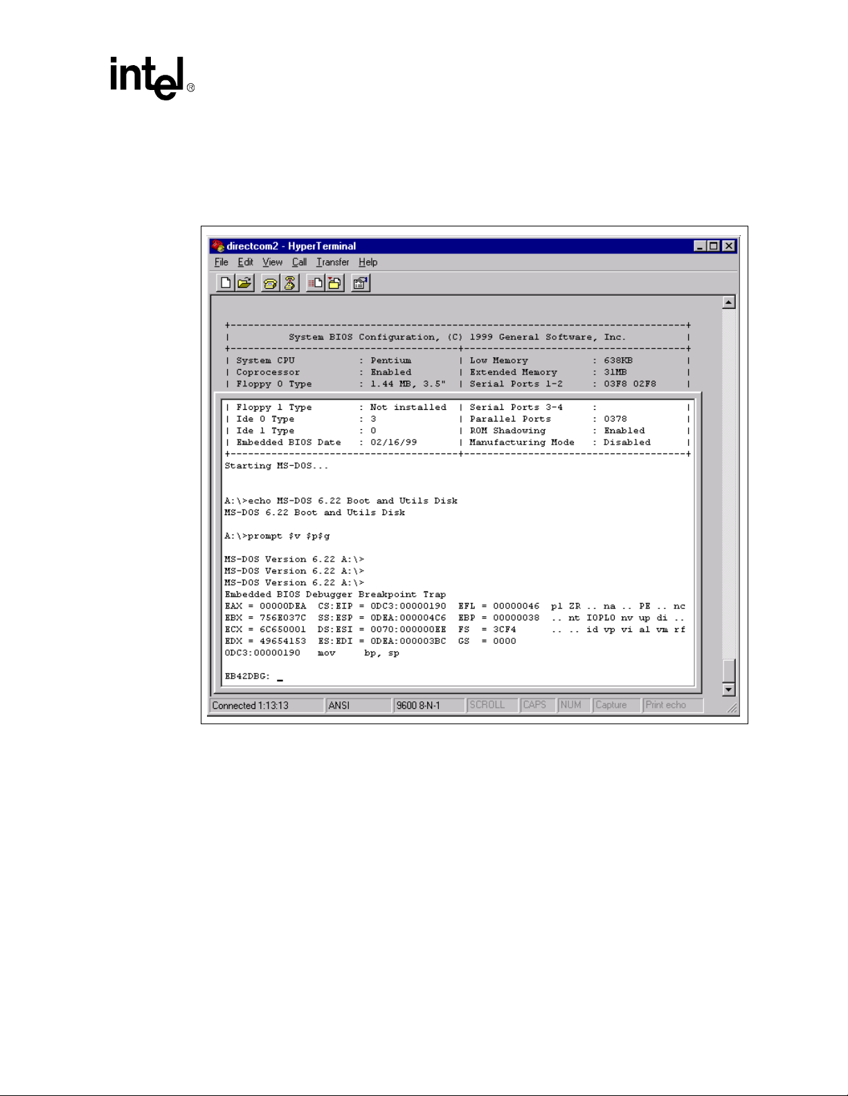
T o activate the debugg er at any time fr om the main console, p ress the left shift and the contro l keys
together. A display similar to the one in the HYPERTERMINAL session below (Figure 5-9) will
appear, containing the title, “Embedded BIOS Debugger Breakpoint Trap” and a snapshot of the
processor general registers.
Figure 5-9. Integrated BIOS Debugger Running Over a Remote Terminal
BIOS Quick Reference
To leave the debugger and resume the interrupted activity (whether POST, BIOS, DOS, Windows,
or an application program), enter the “G” command (short for “go”) and press ENTER. If you were
at a DOS prompt when you entered the debugger, then DOS will still be waiting for its comman d,
and will not prompt again until y ou press ENTER again.
The debugger can also be entered from the Setup Screen System, and as a b oot activity (see “Basic
CMOS Configuration Screen” on page 5-3), as a la st ditch effort during board b ring-up and
development if no bootable device is available.
If your version of DOS, an application, or any OEM-supplied BIOS extensions have debugging
code (i.e., “INT 3” instructions) remaining, then these will invoke the debugger automatically,
although this is not an error. To continue, use the “G” command. When Embedded BIOS is adapted
by the OEM, the debugger can be removed from the final production BIOS, and superfluous
debugging code in the applicat ion will not cause the debugger to be invoked.
Celeron™ Processor Development Kit Manual
5-11
Page 52

BIOS Quick Reference
A complete discussion of the debugger is beyond the scope of this chapter; however, complete
documentation is available from General Software via the web at http://www.gensw.com.
5.11 Embedded BIOS POST Codes
Embedded BIOS writes progress cod es, als o kno wn as P OST codes , t o I/O port 80H during POST,
in order to provide information to OEM developers about system faults. These POST codes may be
monitored on the on-board Post Code Debugg er located at U12 and U13. They ar e not displayed on
the screen. For more information about POST codes, contact General Software.
Mnemonic Code Code System Progress Report
POST_STATUS_START 00h Start POST (BIOS is executing).
POST_STATUS_CPUTEST 01h Start CPU register test.
POST_STATUS_DELAY 02h Start power-on delay.
POST_STATUS_DELAYDONE 03h Power-on delay finished.
POST_STATUS_KBDBATRDY 04h Keyboard BAT finished.
POST_STATUS_DISABSHADOW 05h Disable shadowing & cache.
POST_STATUS_CALCCKSUM 06h Compute ROM CRC, wait for KBC.
POST_STATUS_CKSUMGOOD 07h CRC okay, KBC ready.
POST_STATUS_BATVRFY 08h Verifying BAT command to KB.
POST_STATUS_KBDCMD 09h Start KBC command.
POST_STATUS_KBDDATA 0ah Start KBC data.
POST_STATUS_BLKUNBLK 0bh Start pin 23,24 blocking & unblocking.
POST_STATUS_KBDNOP 0ch Start KBC NOP command.
POST_STATUS_SHUTTEST 0dh Test CMOS RAM shutdown register.
POST_STATUS_CMOSDIAG 0eh Check CMOS checksum.
POST_STATUS_CMOSINIT 0fh Initialize CMOS contents.
POST_STATUS_CMOSSTATUS 10h Initialize CMOS status for date/time.
POST_STATUS_DISABDMAINT 11h Disable DMA, PICs.
POST_STATUS_DISABPORTB 12h Disable Port B, video display.
POST_STATUS_BOARD 13h Initialize board, start memory bank detection.
POST_STATUS_TESTTIMER 14h Start timer tests.
POST_STATUS_TESTTIMER2 15h Test 8254 T2, for speaker, port B.
POST_STATUS_TESTTIMER1 16h Test 8254 T1, for refresh.
POST_STATUS_TESTTIMER0 17h Test 8254 T0, for 18.2Hz.
POST_STATUS_MEMREFRESH 18h Start memory refresh.
POST_STATUS_TESTREFRESH 19h Test memory refresh.
POST_STATUS_TEST15US 1ah Test 15usec refresh ON/OFF time.
POST_STATUS_TEST64KB 1bh Test base 64KB memory.
POST_STATUS_TESTDATA 1ch Test data lines.
POST_STATUS_TESTADDR 20h Test address lines.
POST_STATUS_TESTPARITY 21h Test parity (toggling).
POST_STATUS_TESTMEMRDWR 22h Test Base 64KB memory.
POST_STATUS_SYSINIT 23h Prepare system for IVT initialization.
POST_STATUS_INITVECTORS 24h Initialize vector table.
POST_STATUS_8042TURBO 25h Read 8042 for turbo switch setting.
POST_STATUS_POSTTURBO 26h Initialize turbo data.
POST_STATUS_POSTVECTORS 27h Modification of IVT.
POST_STATUS_MONOMODE 28h Video in monochrome mode verified.
POST_STATUS_COLORMODE 29h Video in color mode verified.
POST_STATUS_TOGGLEPARITY 2ah Toggle parity before video ROM test.
POST_STATUS_INITBEFOREVIDEO 2bh Initialize before video ROM check.
5-12
Celeron™ Processor Development Kit Manual
Page 53

BIOS Quick Reference
POST_STATUS_VIDEOROM 2ch Passing control to video ROM.
POST_STATUS_POSTVIDEO 2dh Control returned from video ROM.
POST_STATUS_CHECKEGAVGA 2eh Check for EGA/VGA adapter.
POST_STATUS_TESTVIDEOMEMORY 2fh No EGA/VGA found, test video memory.
POST_STATUS_RETRACE 30h Scan for video retrace signal.
POST_STATUS_ALTDISPLAY 31h Primary retrace failed.
POST_STATUS_ALTRETRACE 32h Alternate found.
POST_STATUS_VRFYSWADAPTER 33h Verify video switches.
POST_STATUS_SETDISPMODE 34h Establish display mode.
POST_STATUS_CHECKSEG40A 35h Initialize ROM BIOS data area.
POST_STATUS_SETCURSOR 36h Set cursor for power-on msg.
POST_STATUS_PWRONDISPLAY 37h Display power-on message.
POST_STATUS_SAVECURSOR 38h Save cursor position.
POST_STATUS_BIOSIDENT 39h Display BIOS identification string.
POST_STATUS_HITDEL 3ah Display "Hit <DEL> to ..." message.
POST_STATUS_VIRTUAL 40h Prepare protected mode test.
POST_STATUS_DESCR 41h Prepare descriptor tables.
POST_STATUS_ENTERVM 42h Enter virtual mode for memory test.
POST_STATUS_ENABINT 43h Enable interrupts for diagnostics mode.
POST_STATUS_CHECKWRAP1 44h Initialize data for memory wrap test.
POST_STATUS_CHECKWRAP2 45h Test for wrap, find total memory size.
POST_STATUS_HIGHPATTERNS 46h Write extended memory test patterns.
POST_STATUS_LOWPATTERNS 47h Write conventional memory test patterns.
POST_STATUS_FINDLOWMEM 48h Find low memory size from patterns.
POST_STATUS_FINDHIMEM 49h Find high memory size from patterns.
POST_STATUS_CHECKSEG40B 4ah Verify ROM BIOS data area again.
POST_STATUS_CHECKDEL 4bh Check for <DEL> pressed.
POST_STATUS_CLREXTMEM 4ch Clear extended memory for soft reset.
POST_STATUS_SAVEMEMSIZE 4dh Save memory size.
POST_STATUS_COLD64TEST 4eh Cold boot: Display 1st 64KB memtest.
POST_STATUS_COLDLOWTEST 4fh Cold boot: Test all of low memory.
POST_STATUS_ADJUSTLOW 50h Adjust memory size for EBDA usage.
POST_STATUS_COLDHITEST 51h Cold boot: Test high memory.
POST_STATUS_REALMODETEST 52h Prepare for shutdown to real mode.
POST_STATUS_ENTERREAL 53h Return to real mode.
POST_STATUS_SHUTDOWN 54h Shutdown successful.
POST_STATUS_DISABA20 55h Disable A20 line.
POST_STATUS_CHECKSEG40C 56h Check ROM BIOS data area again.
POST_STATUS_CHECKSEG40D 57h Check ROM BIOS data area again.
POST_STATUS_CLRHITDEL 58h Clear "Hit <DEL>" message.
POST_STATUS_TESTDMAPAGE 59h Test DMA page register file.
POST_STATUS_VRFYDISPMEM 60h Verify from display memory.
POST_STATUS_TESTDMA0BASE 61h Test DMA0 base register.
POST_STATUS_TESTDMA1BASE 62h Test DMA1 base register.
POST_STATUS_CHECKSEG40E 63h Checking ROM BIOS data area again.
POST_STATUS_CHECKSEG40F 64h Checking ROM BIOS data area again.
POST_STATUS_PROGDMA 65h Program DMA controllers.
POST_STATUS_INITINTCTRL 66h Initialize PICs.
POST_STATUS_STARTKBDTEST 67h Start keyboard test.
POST_STATUS_KBDRESET 80h Issue KB reset command.
POST_STATUS_CHECKSTUCKKEYS 81h Check for stuck keys.
POST_STATUS_INITCIRCBUFFER 82h Initialize circular buffer.
POST_STATUS_CHECKLOCKEDKEYS 83h Check for locked keys.
POST_STATUS_MEMSIZEMISMATCH 84h Check for memory size mismatch.
POST_STATUS_PASSWORD 85h Check for password or bypass setup.
Celeron™ Processor Development Kit Manual
5-13
Page 54

BIOS Quick Reference
POST_STATUS_BEFORESETUP 86h Password accepted.
POST_STATUS_CALLSETUP 87h Entering setup system.
POST_STATUS_POSTSETUP 88h Setup system exited.
POST_STATUS_DISPPWRON 89h Display power-on screen message.
POST_STATUS_DISPWAIT 8ah Display "Wait..." message.
POST_STATUS_ENABSHADOW 8bh Shadow system & video BIOS.
POST_STATUS_STDCMOSSETUP 8ch Load standard setup values from CMOS.
POST_STATUS_MOUSE 8dh Test and initialize mouse.
POST_STATUS_FLOPPY 8eh Test floppy disks.
POST_STATUS_CONFIGFLOPPY 8fh Configure floppy drives.
POST_STATUS_IDE 90h Test hard disks.
POST_STATUS_CONFIGIDE 91h Configure IDE drives.
POST_STATUS_CHECKSEG40G 92h Checking ROM BIOS data area.
POST_STATUS_CHECKSEG40H 93h Checking ROM BIOS data area.
POST_STATUS_SETMEMSIZE 94h Set base & extended memory sizes.
POST_STATUS_SIZEADJUST 95h Adjust low memory size for EBDA.
POST_STATUS_INITC8000 96h Initialize before calling C800h ROM.
POST_STATUS_CALLC8000 97h Call ROM BIOS extension at C800h.
POST_STATUS_POSTC8000 98h ROM C800h extension returned.
POST_STATUS_TIMERPRNBASE 99h Configure timer/printer data.
POST_STATUS_SERIALBASE 9ah Configure serial port base addresses.
POST_STATUS_INITBEFORENPX 9bh Prepare to initialize coprocessor.
POST_STATUS_INITNPX 9ch Initialize numeric coprocessor.
POST_STATUS_POSTNPX 9dh Numeric coprocessor initialized.
POST_STATUS_CHECKLOCKS 9eh Check KB settings.
POST_STATUS_ISSUEKBDID 9fh Issue keyboard ID command.
POST_STATUS_RESETID 0a0h KB ID flag reset.
POST_STATUS_TESTCACHE 0a1h Test cache memory.
POST_STATUS_DISPSOFTERR 0a2h Display soft errors.
POST_STATUS_TYPEMATIC 0a3h Set keyboard typematic rate.
POST_STATUS_MEMWAIT 0a4h Program memory wait states.
POST_STATUS_CLRSCR 0a5h Clear screen.
POST_STATUS_ENABPTYNMI 0a6h Enable parity and NMIs.
POST_STATUS_INITE000 0a7h Initialize before calling ROM at E000h.
POST_STATUS_CALLE000 0a8h Call ROM BIOS extension at E000h.
POST_STATUS_POSTE000 0a9h ROM extension returned.
POST_STATUS_DISPCONFIG 0b0h Display system configuration box.
POST_STATUS_INT19BOOT 00h Call INT 19h bootstrap loader.
POST_STATUS_LOWMEMEXH 0b1h Test low memory exhaustively.
POST_STATUS_EXTMEMEXH 0b2h Test extended memory exhaustively.
POST_STATUS_PCIENUM 0b3h Enumerate PCI busses.
5-14
Celeron™ Processor Development Kit Manual
Page 55

5.12 Embedded BIOS Beep Codes
Embedded BIOS tests much of the system hardware early in POST before messages can be
displayed on the screen. When system failures are encountered at these early stages, POST uses
beep codes (a sequence of tones on the speaker) to identify the source of the error.
The following is a comprehensive list of POST beep codes for the system BIOS. BIOS extensions,
such as VGA ROMs and SCSI adapter ROMs, may use their o wn b eep codes, including short/long
sequences, or possibly beep codes that sound like the ones below. When diagnosing a system
failure, remove these adapters if possible before making a final determ ination of the actual POST
test that failed.
Mnemonic Code Beep CountDescription of Problem
POST_BEEP_REFRESH 1 Memory refresh is not working.
POST_BEEP_PARITY 2 Parity error found in 1st 64KB of memory.
POST_BEEP_BASE64KB 3 Memory test of 1st 64KB failed.
POST_BEEP_TIMER 4 T1 timer test failed.
POST_BEEP_CPU 5 CPU test failed.
POST_BEEP_GATEA20 6 Gate A20 test failed.
POST_BEEP_DMA 7 DMA page/base register test failed.
POST_BEEP_VIDEO 8 Video controller test failed.
POST_BEEP_KEYBOARD 9 Keyboard test failed.
POST_BEEP_SHUTDOWN 10 CMOS shutdown register test failed.
POST_BEEP_CACHE 11 External cache test failed.
POST_BEEP_BOARD 12 General board initialization failed.
POST_BEEP_LOWMEM 13 Exhaustive low memory test failed.
POST_BEEP_EXTMEM 14 Exhaustive extended memory test failed.
POST_BEEP_CMOS 15 CMOS restart byte test failed.
POST_BEEP_ADDRESS_LINE 16 Address line test failed.
POST_BEEP_DATA_LINE 17 Data line test failed.
POST_BEEP_INTERRUPT 18 Interrupt controller test failed.
POST_BEEP_PASSWORD 1 Incorrect password used to access SETUP.
BIOS Quick Reference
Celeron™ Processor Development Kit Manual
5-15
Page 56

Page 57

PLD Code Listing A
The code listing below is for the 22V10 PLD.
TITLE 22V10 PORT 80 ADDRESS DECODER / FLASH DECODE
PATTERN 1
REVISION B
AUTHOR CHRIS BANYAI
COMPANY INTEL CORPORATION
DATE 10/1/97
OPTIONS
SECURITY = OFF
; ( part was 22V10FN before conversion )
CHIP P80B iPLD22V10N
PIN 19 IOWR_BAR
PIN 3 AEN
PIN [6:7] SA[0:1]
PIN [9:13] SA[2:6]
PIN 16 SA7
PIN [5:4] SA[8:9]
PIN [26:23] SA[19:16]
PIN [21:20] SA[15:14]
PIN 2 SEL
PIN 18 /CS_BAR
PIN 17 /CS_DOC
PIN 27 OX
EQUATIONS
CS_BAR = /IOWR_BAR * /AEN * /SA0 * /SA1 * /SA2 * /SA3 * /SA4 * /SA5 * /SA6
* SA7 * /SA8 * /SA9
CS_BAR.TRST = VCC
CS_DOC = /SEL * /AEN * SA19 * SA18 * /SA17 * /SA16 * SA15 * /SA14
+ SEL * /AEN * SA19 * SA18 * /SA17 * SA16 * /SA15 * /SA14
CS_DOC.TRST = VCC
OX = /IOWR_BAR
OX.TRST = VCC
SIMULATION
SETF /AEN /SA0 /SA1 /SA2 /SA3 /SA4 /SA5 /SA6 /SA7 /SA8 /SA9 IOWR_BAR
SETF SA7 IOWR_BAR
SETF /IOWR_BAR
SETF IOWR_BAR
Celeron™ Processor Development Kit Manual
A-1
Page 58

PLD Code Listing
SETF AEN /IOWR_BAR
SETF /AEN
SETF IOWR_BAR
SETF SA0 /IOWR_BAR
SETF /SA0 /IOWR_BAR
SETF IOWR_BAR
SETF /SA0 /SA1 /SA2 /SA3 /SA4 /SA5 /SA6 /SA7 /SA8 /SA9
SETF /SA19 /SA18 /SA17 /SA16 /SA15 /SA14
SETF /SEL
SETF SA19 SA18 /SA17 /SA16 SA15 /SA14
SETF /SEL
SETF /AEN
SETF /SA19
SETF SA19
SETF /SA18
SETF SA18
SETF SA17
SETF /SA17
SETF SA16
SETF /SA16
SETF /SA15
SETF SA15
SETF SA14
SETF /SA14
SETF /SEL
SETF SA19 SA18 /SA17 SA16 /SA15 /SA14
SETF /SEL
SETF /AEN
SETF SEL
SETF /SA19
SETF SA19
SETF /SA18
SETF SA18
SETF SA17
SETF /SA17
SETF /SA16
SETF SA16
SETF SA15
SETF /SA15
SETF SA14
SETF /SA14
SETF /SEL
A-2
Celeron™ Processor Development Kit Manual
Page 59

Bill of Materials B
Table B-1 is the bill of materials for the baseboard. Table B-2 is the bill of materials for the
Processor Assembly.
Table B-1. Baseboard Bill of Materials (Sheet 1 of 4)
Reference Description Manufacturer Manufacturer P/N Notes
J14,J15
J20-24
JP2
J10 NOT POPULATED
J12 Conn,Fan AMP 173981-3
XU9 PLCC, Socket 28 AMP 822271-1
J19
U6
U26
U16
Y2
J17,J18
J4 Conn, Serial Stack,DB9MX2 FOXCONN DM10156-73
J3 Conn, DB25,DB25FM1 FOXCONN DT11323-R5T
J7,J8,J9
J5,J6 Conn,ISA Edge Recept.,isa-98 FOXCONN EQ04901-S6
JP1 Conn,Floppy,17X2 Header FOXCONN HL07173-P4
JP3,JP4 Conn, IDE,20X2 Header FOXCONN HL07206-D2
J11 Conn,Power,5566DP-20/ATX FOXCONN HM20100-P2
J1
J13
J2 2 USB Stack Connectors FOXCONN UB1112C-D3
Conn,Jumper2,1X2 25-mil sq/
100-mil space,HDR2
Conn,Jumper3,1X3 25-mil sq/
100-mil space,HDR3
Conn,Speaker,1X4 25-mil sq/
100-mil space,HDR4
Conn,CPU,400 Pin Array
(BGA),BGA40X10-400R
IC,Clock
Generator,CK100,SSOP30048(PIN)
IC,Clock Buffer,Zero Delay
3.3V,16PIN,150MIL,TSSOP,PSS
OP16
IC,Clock Buffer,18 Output low
skew,SSOP300-48(PIN)
Crystal,32.768KHz,XTAL/MC405
Conn,SDRAM DIMM,168 Pin
Recept
Conn,PCI Edge Recept,145154120
Conn,PS2 Keyboard / Mouse
Connector
Conn,AGP Edge Recept., 120
pins,AGP-124
3M 929647-09-02
3M 929647-09-03
3M 929647-09-04
Berg 74219-002
Cypress CY2280PVC-11S
Cypress CY2309ZC-1H
Cypress CY2318ANZPVC-1
Epson MC-405
FOXCONN AT08403-K8
FOXCONN EH06001-PC-W
FOXCONN MH11067-D2
FOXCONN PC1243K-10
DO NOT
POPULATE
DO NOT
POPULATE
J16
Celeron™ Processor Development Kit Manual
B-1
Page 60

Bill of Materials
Table B-1. Baseboard Bill of Materials (Sheet 2 of 4)
Reference Description M anufact urer Manufacturer P/N Notes
U11
U8
U14
C99,C100,C132,C133,C2
09,C214
C: 22,42-43,48-49,54,59-
65,70-71,73,75-76,8587,90-92,96-97, 102,106108,111-112,114,116-1 18,
126-127,129131,142,147,157,159-162,
174-176,181-183, 187200,205-206,208,226-228
C27-C41,C44-C47,C50C53
C3-5,C8,C55-57,
C94,C119-121,
C134,C138,C145, C153
C93,C103-105,
C128,C152, C154-156
C2,C6,C58,C72,
C84,C88,C89,C95, C109
C1,C7,C23,C66C68,C74,C77-C82,
C101,C113,C115,
C141,C158,C163173,C177-180, C184186,C201202,C204,C207, C211213,C216-217,C220-C225
U9 IC,PLD,PLCC28,Socket28 LATTICE GAL22V10B-7LJ
U23
U5
XU11
XU12,XU13 TIL311 SOCKET,DIP14 MILLMAX 110-99-314-41-001
U25 IC,Logic,74ACT05,SO14 Motorola MC74ACT05DR
FB1-FB9 Ferrite Bead,SM1806,Z-Bead Murata BLM41A800S
U22 IC,Logic,74ALS00,SOIC14 National DM74ALS00M
U7
C69,C83,C98,C110
BIOS FLASH
Memory,TSOP12X20/40S
VLSI,PIIX4,PCI to IDE &ISA
Bridge,324 mBGA,BGA20x20324
IC,Interrupt Controller,
82093AA,QFP16x22-64
Chip Capacitor,10pF,
50V,CC0603
Chip Capacitor,0.1uF,
16V,CC0603
Chip Capacitor,470pF,
50V,CC0603
Cap,Tant,10uF,15V,C Case,6032 Kemet T491C106K016AS
Cap,Tant,47uF, 20V,D
Case,7343
Cap,Tant,100uF, 10V,D
Case,7343
Chip Capacitor,0.01uF
50V,CC0603
IC,Linear Voltage
Regulator,SOT-223
IC,Linear Voltage
Regulator,SOT-223
40TSOP BIOS
Socket,TSOP12X20/40S
IC,Tranciever,8-Bit Bidirectional
Buffer,SOIC20,SO20W
Cap,Electrolitic,220uF,
25v,6.3mmx11.2mm,PCAPR200
-300
INTEL 28F002BC
Intel FW82371EB
INTEL S82093AA
Kemet C0603C100J5GAC
Kemet C0603C104K4RAC
Kemet C0603C471K5RAC
Kemet T491D476M020AS
Kemet T495D107M010AS
Kemet C0603C103J5RAC
Linear Tech. LT11 17-3.3cst
Linear Tech. LT1117CST
Meritec 980020-40-01
National DM74ALS245AWM
Panasonic ECE-A1EU221
DO NOT
POPULATE
DO NOT
POPULATE
C143,
C146,C203,
C210, C215
B-2
Celeron™ Processor Development Kit Manual
Page 61

Table B-1. Baseboard Bill of Materials (Sheet 3 of 4)
Reference Description Manufacturer Manufacturer P/N Notes
R33,R35,R37,R48,R52,R9
8-R100, R106,R108R116,R118-R122
R6,R25,R42,R45,R49R51,R63,R101,R102
R2,R4,R5,R11,R40,R41,R
43,R53R56,R97,R105,R117,R123
-124,R127
R1,R3,R88,R89.R90,R91 Chip Resistor,15K,5%,CR0805 Panasonic ERJ6GEYJ15 3V
R9 Chip Resistor,22,5%,CR0805 Panasonic ERJ6GEYJ220V
R10,R12,R13,R14,R39,R5
8,R70
R92-R95 Chip Resistor,27,5%,CR0805 Panasonic ERJ6GEYJ270V
R20,R44,R57,R71 Chip Resistor,2.7K,5%,CR0805 Panasonic E RJ6GE YJ272V
R17-R19,R21-R24,R26-
R32,R34,R36,R38
R103,R104 Chip Resistor,470,5%,CR0805 Pa nasonic ERJ6GEYJ471V
R7,R64-R69,
R125,R126,R128
R72-R87,R96,R107 Chip Resistor,8.2K,5%,CR0805 Panasonic ERJ6GEYJ822V
S1,S2
RP2,RP3,RP41-
RP47,RP54-RP56,
RP58,RP60,RP61
RP10,RP18,RP23 Res,Array,SMT ,1K,5%,EXB-V Panasonic EXB38V102JV
RP8-9,RP11,RP13-
17,RP19-RP22,
RP24,RP26-33, RP35-36,
RP39, RP51-52,RP59
RP1,RP4,RP48 Res,Array,SMT,22,5%,EXB-V Panasonic EXB38V220JV
RP25,RP37,RP38,RP40,R
P49,RP50,RP53
RP57 Res,Array,SMT,47,5%,EXB-V Panasonic EXB38V470JV
RP5,RP6,RP7 Res,Array,SMT,4.7K,5%,EXB-V Panasonic EXB38V472JV
RP12,RP34 Res,Array,SMT,5.6k,5%,EXB-V Panasonic
U24
U10
Y1
F1-F3 Fuse,Drawing,SM250 RayChem SMD250-2
Chip Resistor,0 Ohm
Shunt,5%,CR0805
Chip Resistor,1K,5%,CR0805 Panasonic E RJ6GE YJ10 2 V
Chip Resistor,10K,5%,CR0805 Panasonic ERJ6GEYJ103V
Chip Resistor,220,5%,CR0805 Pa nasonic ERJ6GEYJ221V
Chip Resistor,33,5%,CR0805 Panasonic ERJ6GEYJ33 0V
Chip Resistor,4.7k,5%,CR0805 Panasonic ERJ6GEYJ472V
Switch-Push Button,PBSW/
PNASNC2
Res,Array,SMT,33,5%,EXB-V Panasonic EXB33V330JV
Res,Array,SMT,10K,5%,EXB-V Panasonic EXB38V103JV
Res,Array,SMT,2.7K,5%,EXB-V Panasonic EXB38V272JV
IC,Logic,Inverter, Schmitt
Trigger,SOIC14
IC,Logic,10 Bit Bus
Switch,QSOP,SO24W
Crystal,14.318MHz,XTAL,FOXHC495D
Panasonic ERJ6GEY0R00V
Panasonic EVQ-PHP03T
Philips 74HCT14D
Quality Semi QS3384SO
Raltron AS-14.31818-20
Bill of Materials
DO NOT
POPULATE
R33, R35,
R37
DO NOT
POPULATE
R6, R51
Celeron™ Processor Development Kit Manual
B-3
Page 62

Bill of Materials
Table B-1. Baseboard Bill of Materials (Sheet 4 of 4)
Reference Description M anufact urer Manufacturer P/N Notes
XBT1 Battery Holder Socket Renata HU-2032-1
BT1 Battery Reneta CR2032
D1,D2,D5 Diode,LED,SOT23-A Siemens LGS260-DO
U1 VLSI,Super I/O,QFP128 S MSC FDC37B78X
C122-C125,C229 Chip Capacitor,47pF,CC0603 TDK C1608C0G1H470JT$
C9-C21,C24-C26 Chip Capacitor,220pF,CC0603 TDK C1608X7R1H221KT009A
U15 IC,Logic,3 state buffer,SOP-14 TI 74LVC125A
U21 IC,Logic,SOP-14 TI 74LVC14A
U3,U4
U2
U12,U13 7 Segment LED display,DIP14 TI TIL311
D3-D4,D6-D7 Schottky Diode,SOT23-E ZETEX BAT54
R8,R15,R16,R46,R47 Chip Resistor,124,1%,CR0805
IC,RS232 Transceiver,
SOIC20,SO20W
IC,Logic,Open Drain Buffer,SOP14
32 MB SDRAM DIMMS
TI GD75232DW
TI SN7407D
Micron
Semiconductor
Prdcts
MT4LSDT464AG-662B2
DO NOT
POPULATE
C229
B-4
Celeron™ Processor Development Kit Manual
Page 63

Bill of Materials
Table B-2. Celeron™ Processor Assembly Bill of Materials (Sheet 1 of 2)
Reference Descriptions Manufacturer Manufacturer P/N
C1 CAP 20 pF 25V CC0603 Panasonic ECU-V1H200J CM
C117 CAP 4700pF 50V CC0603 Panasonic ECJ-1VB1H472K
C84-C85, C94-C98 CAP 0.01uF 10V CC0603 Panasonic ECJ-1VB1C103K
C2-9, C48,C50-83,C86-
93,C100103,C106,C1 10,C113,C115,C
116,C128-C129,C131C132,C137-C138, C140C142,C145-C146
C10-C24,C30-C34,C40C44,C112, C114,C126,C133136
C25-C29,C35-C39,C45C47,C139
C122-C125 CAP 10uF 16V CC1210 Panasonic Do Not Populate
C49 CAP 33uF 16V 3528 Kernet T491B226M010AS
C104-C105,C127,C130, CAP 470uF 16V
C107-C109,C111,C118-C121 CAP 2200uF 16V
D1 Diode BAT54 SOT23 Zetex BAT54CT-ND
L1 Inductor 22 uH CR0805 Murata LQG21C220N00T1
L2,L3 I nductor 4.7uH IND1855 Bi Technologies HM00-98637A
Q1
RP1-RP2 Resistor Pac 1K EXB-V Panasonic EXB-V8V102JV
RP33-RP62 Resistor Pac 56 ohm EXB-V Panasonic EXB-V8V560JV
RP63 Resistor Pac 330 EXB-V Panasonic EXB-V8V331JV
R9,R12,R54,R66,R78,R79 Resistor 0 CR0805 Panasonic ERJ-6GEY0R00V
R14 Resistor 1.1 CR0805 Panasonic ERX-1SJ1R1
R68,R71,R72 Resistor 2.2 CR1206 Panasonic ERJ-6RQJ2R2V
R65,R63 Resistor 10 CR0805 Panasonic ERJ-6GEYJ100V
R19,R26-R27 Resistor 22 CR0805 Panasonic ERJ-6GEYJ220V
R4,R41,R48,R50,R51,R77 Resistor 51 CR0805 Panasonic ERJ-6GEYJ510V
R1,R7,R8,R31,R46,R47,R49,
R52
R10 Resistor 330 CR0805 Panasonic ERJ-6GEYJ331V
R2-R3, R15,R32-R39,R42-
R43,R45,R53,R64,R67,R80
R11,R13, R40,R44 Resistor 3.3K CR0805 Panasonic ERJ-6GEYJ332V
R16-R18,R20-R25,R28-
R30,R70
CAP 0.1uF 16V CC0603 Panasonic ECJ-1VB1C104K
CAP 1uF 10V CC0805 Panasonic ECJ-2YB1A105K
CAP 4.7uF 10V CC1206 Panasonic ECJ-3YF1C475Z
PCAPR20
0-300
PCAPR20
0-500
NPN
Transistor
Resistor 270 CR0805 Panasonic ERJ-6GEYJ271V
Resistor 1K CR0805 Panasonic ERJ-6GEYJ102V
Resistor 10K CR0805 Panasonic ERJ-6GEYJ102V
MMBT3904 SOT23 Fairchild MMBT3904
Panasonic EEU-FC1C471L
Panasonic EEU-FC1C222
Celeron™ Processor Development Kit Manual
B-5
Page 64

Bill of Materials
Table B-2. Celeron™ Processor Assembly Bill of Materials (Sheet 2 of 2)
Reference Descriptions Manufacturer Manufacturer P/N
R75,R73 Resistor 47K CR0805 Panasonic ERJ-6GEYJ472V
R55,R56 Resistor 75 1% CR0805 Panasonic ERJ-6ENF0750V
R60 Resistor 100 1% CR0805 Panasonic ERJ-6ENF1000V
R6,R5 Resistor 110 1% CR0805 Panasonic ERJ-6ENF1100V
R57-R59 Resistor 150 1% CR0805 Panasonic ERJ-6ENF1500V
R61 Resistor 1.00K 1% CR0805 Panasonic ERJ-6ENF1001V
R62 Resistor 2.32K 1% CR0805 Panasonic ERJ-6ENF2321V
R69,R74,R76 Resistor
U2,U3 Logic 74LVC07A SO14
U4 BGA Chip 443BX_10 Intel FW82443BX
U5
U6 Temp Sensor MAX1617 QSOP16 Maxim MAX1617MEE
U7 Logic QS3257 SO16 Quickswitch QS3257
U8 Logic 74LVQ00 SO14
U9 Logic SC1185 SO24W Semtech SC1185
U10,U11 FET
U12,U13 FET MTD3055V TO252 Motorola MTD3055V
U1
XU1
J2 Header ITP 104068-3 AMP 104068-3
J1 Connector
J3 Connector 4 Pin PWR 644518-4 AMP 644518-4
BGA
Connector
Processor, 370-pin, 37x37 PPGA, 366 MHz
OR (depends on kit purchased)
Processor, 370-pin, 37x37 PPGA, 433 MHz
Socket Socket370 AMP 916783-2
Socket Socket370 Foxconn PZ37047S1T-S-001
3 milliOhm
5%
SUD50N0307
Fan
Connector
CR2512 Dale/Vishay WSL-2512 0.003 5%
Texas
Instruments
BGA40X1
0-400
TO252 Siliconix SUD50N03-07-T4
173981-3 AMP 173981-3
Berg 74220-001
National
Semiconductor
Intel
SN74LVC07AD
74LVQ00
FV80524RX366128
FV80524RX433128
B-6
Celeron™ Processor Development Kit Manual
Page 65

Schematics C
The most current schematics, including “flat” schematics (without the 400-pin connector), are
located on Intel’s Developer Web site at: http://w ww.intel.com/design/intarch/schems/.
Schematics are provided for the following items:
Baseboard:
• Block Diagram
• Mini-PCI Connector (Not Populated)
• Processor Assembly Connector
• DIMM0
• DIMM1
• DIMM2 (Not Populated)
• Clocks
• ISA/PCI Pullups
• PCI Slots 0 & 1
• PCI Slot 2
• AGP Connector
• PIIX4 Part 1
• PIIX4 Part 2
• IDE Connectors
• Super I/O
• USB Connectors
• ISA Connectors
• COMx, DB25, Floppy
• BIOS/ Port 80
• ATX Power Connector
• Unused Gates
Processor Assembly:
• Socket 370A Host Interface
• Socket 370B Power Supply
• GTL+ Termination Resistors - Bridge System/Co ntroller
• GTL+ Termination Resistors - Processor
• 82443BX - Bus Interface
• 82443BX - Memory Interface
• Connector Hardware
• ITP/Bus Ratio/Thermal Sensor
• Voltage Regulator
Celeron™ Processor Development Kit Manual
C-1
Page 66
D
of
1 22Thursday, February 25, 1999
1
2
Changes
Title
1
C
Size Document Number Rev
Date: Sheet
2
THIS DRAWING CONTAINS INFORMATION WHICH HAS NOT
BEEN VERIFIED FOR MANUFACTURING AS AN END USER
PRODUCT. INTEL IS NOT RESPONSIBLE FOR THE
3
MISUSE OF THIS INFORMATION.
3
Revision D
Evaluation Platform
System Electronics Board
4
THIS SCHEMATIC IS PROVIDED "AS IS" WITH NO WARRANTIES WHATSOEVER, INCLUDING
No license, express or implied, by estoppel or
ANY WARRANTY OF MERCHANTABILITY, FITNESS FOR ANY PARTICULAR PURPOSE, OR ANY
WARRANTY OTHERWISE ARISING OUT OF PROPOSAL, SPECIFICATION OR SAMPLE.
otherwise, to any intellectual property rights is
granted herein.
Intel disclaims all liability, including liability
for infringement of any proprietary rights, relating
to use of information in this specification. Intel
does not warrant or represent that such use will not
infringe such rights.
4
History
1. Swapped AD23 and AD19 on 400 pin connector.
2. Separated CSEL on IDE0 and IDE1
3. Swapped pins 1 and 3 (V5 with TP) on CPU-Fan connector.
4. Tied VBAT (pin 65) to 5.0V on Super I/O.
5. Changed RP48 to 4.7K. (Pullups for mouse and keyboard.)
6. Inverted POWERON# signal (SUSC#) from PIIX4 to control soft-on feature.
7. Changed Bulk decoupling on +12 and -12 to 2x220uF from 2x400uF.
Changes made to Revision D.
1. Added Signals PWROK(A24) +12V(A33) MB12#_R(B33) to J19A.
Changes made to Revision C.
1. Tied VBAT (pin 65) to 3.3V on Super I/O.
2. Moved J20
3. Added C229 to -PCIRST
Changes made to Revision B.
8. Changed Bulk decoupling cap C154 from 10uF to 47uF to reduce BOM line items.
5
D D
C C
B B
A A
5
Page 67
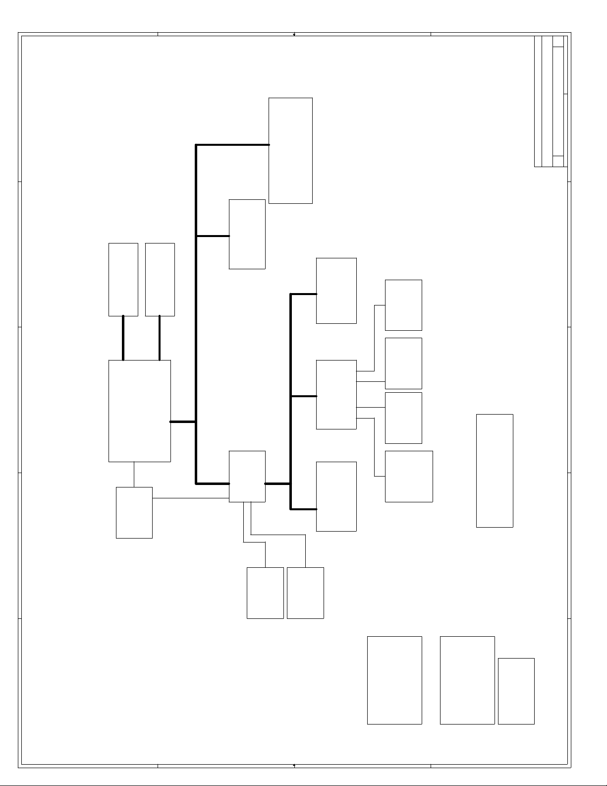
D
2 22Thursday, February 25, 1999
E
Micro Flash
Connector
Page 3
D
DRAM (DIMM)
AGP Port
Page 12
Page 5,6,7
PCI BUS
C
PCI
Connectors
Page 10,11
ISA BUS
ISA
Connectors
Page 18
Floppy
Page 19
Parallel
Page 19
Shakopee
Title
THIS DRAWING CONTAINS INFORMATION WHICH HAS NOT
BEEN VERIFIED FOR MANUFACTURING AS AN END USER
{Doc}
C
Size Document Number Rev
PRODUCT. INTEL IS NOT RESPONSIBLE FOR THE
MISUSE OF THIS INFORMATION.
E
Date: Sheet of
D
C
Super I/O
Page 16
Serial
Page
19
CPU Module
Connector
Page 4
PIIX4
Page
13,14
Flash Bios
Port 80
Page 20
APIC
Page
13
B
IDE
Page15USB
A
Page
17
PS2
KBD/MS
Page
Clocks
Page 8
16
Unused
Power
Page
21
Devices
Page 22
Pullups
Page 9
B
A
4 4
3 3
2 2
1 1
Page 68

D
3 22Thursday, February 25, 1999
E
D
AD31
R70
220
-FRAME 4,9,10,11,13
-PLOCK 4,9,10,11
-DEVSEL 4,9,10,11,13
-IRDY 4,9,10,11,13
-TRDY 4,9,10,11,13
-STOP 4,9,10,11,13
-PCIRST 4,10,11,12,13
PAR 4,9,10,11,13
-SERR 4,9,10,11,13
-PREQ3 4,9,13
-PGNT3 4,9
CLKRUN# 4,13
C
V5_0
V5_0
PIRQD# 9,10,11,13,14
PIRQC# 9,10,11,12,13,14
PIRQB# 9,10,11,12,13,14
PIRQA# 9,10,11,13,14
-PERR 9,10,11
IDSELF
THIS DRAWING CONTAINS INFORMATION WHICH HAS NOT
E
Mini PCI Connector
{Doc}
C
Title
Size Document Number Rev
Date: Sheet of
D
BEEN VERIFIED FOR MANUFACTURING AS AN END USER
PRODUCT. INTEL IS NOT RESPONSIBLE FOR THE
MISUSE OF THIS INFORMATION.
C
7172737475767778798081828384858687888990919293949596979899
7172737475767778798081828384858687888990919293949596979899
J10
V3_3 V3_3
AD0
AD1
AD2
AD3
AD4
AD5
AD6
AD7
B
PCICLK48
AD[31:0]4,10,11,13
A
100
101
102
103
104
105
106
107
108
109
110
111
112
113
114
115
116
117
118
119
120
121
122
123
124
125
126
127
128
129
130
131
132
133
134
135
136
137
138
139
140
100
101
102
103
104
105
106
107
108
109
110
111
112
113
114
115
116
117
118
119
120
121
122
123
124
125
126
127
128
129
130
131
132
133
134
135
136
137
138
139
140
321332343354365376387398409411042114312441345144615471648174918501951205221532254235524562557265827592860296130623163646566676869
321332343354365376387398409411042114312441345144615471648174918501951205221532254235524562557265827592860296130623163646566676869
AD30
-C/BE0
-C/BE1
AD31
-C/BE2
-C/BE3
AD8
AD9
AD10
AD11
AD12
AD13
AD14
AD15
AD16
AD17
AD18
AD19
AD20
AD21
AD22
AD23
AD24
AD25
AD26
AD27
AD28
AD29
2X70RCPT
70
70
V5_0
B
-C/BE[3:0]4,10,11,13
A
4 4
3 3
2 2
1 1
Page 69
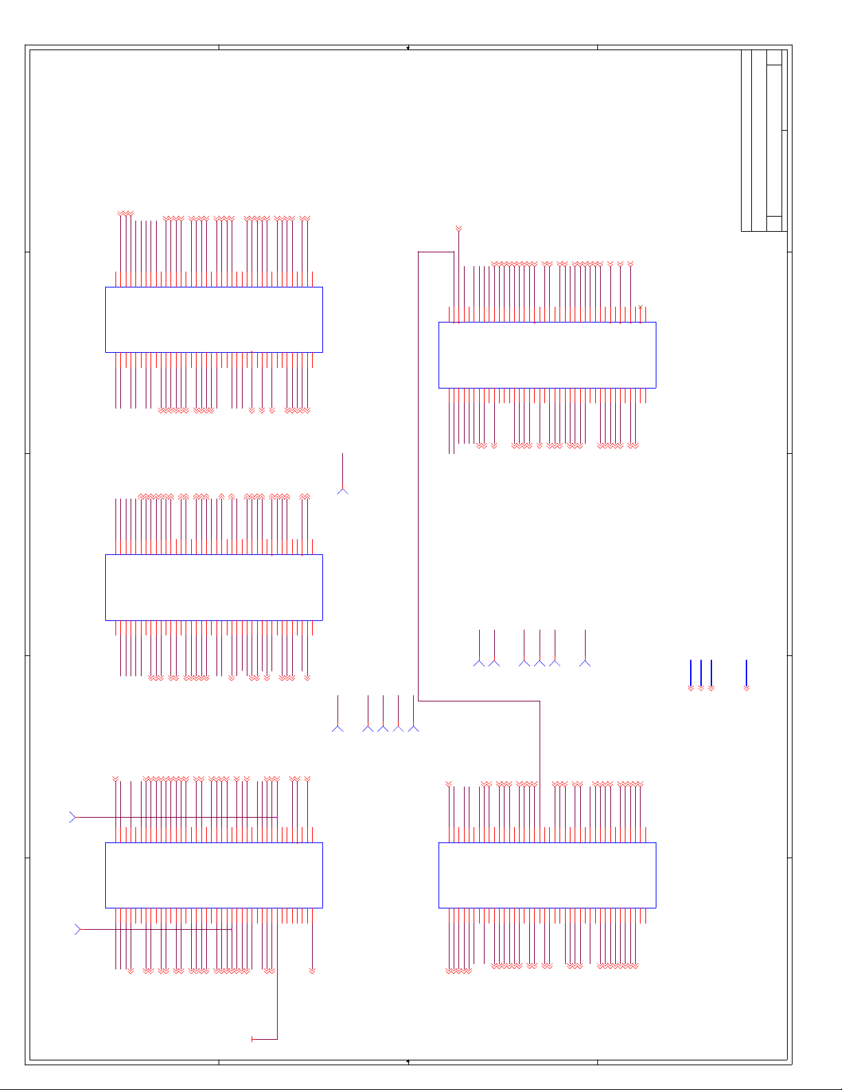
D
4 22Thursday, February 25, 1999
E
GGNT# 12
GST0 12
GREQ# 12
F2
F1
F3
GND
G_REQ#
SBA0
D
SBA7
J19C
E2
E1
SBA7
SBA0
GAD31
SBA4
GAD27
F4E3F5
ST0
V3_3
GAD8
GAD6
GAD13
GAD12
F6E4F7
G_AD13
G_GNT#
G_AD8
G_C/BE0#
GC/BE#0
GAD5
GAD10
GAD11
F8E5F9E6F10E7F11
G_AD12
G_AD10
GND
G_AD7
GAD7
GAD0
GAD_STB0 12
CLKRUN# 3,13
GAD9
G_AD9
G_AD11
V3_3
G_AD0
MD32 5,6,7
MD35 5,6,7
GND
MD34
E10
MD345,6,7
MD6 5,6,7
AD0 3,10,11,13
MECC1 5,6,7
F12E8F13
AD0
MECC1
MD5
MD16
E11
E12
MD55,6,7
MD85,6,7
MD39 5,6,7
MD10 5,6,7
-SERR 3,9,10,11,13
AD16 3,10,11,13
F14E9F15
V3_3
AD16
SERR#
MD17
MD20
MD46
E13
E14
E15
MD95,6,7
MD125,6,7
MD465,6,7
MD13 5,6,7
MD47 5,6,7
AD19 3,10,11,13
AD23 3,10,11,13
F16
F17
AD23
AD19
GND
DQMB1
E16
E17
DQMB17
DQMA1 5,6
AD27 3,10,11,13
-PCIRST 3,10,11,12,13
F18
F19
F20
AD27
PCI_RST#
CSA0#
CSB3#
E18
E19
E20
CS_A0#5
CS_B3#6
DQMA5 5,6
CS_A3# 6
MAB#1
GND
MAA1
MAA15,6
CS_B0# 5
F21
CSB0#
MAB3#
E21
MAB#3
RSV8
-IRDY 3,9,10,11,13
-PGNT3 3,9
-PGNT1 9,10
F22
F23
F24
IRDY#
GNT3#
GNT1#
V3_3
GND
MAB6#
E22
E23
E24
MAB#6
WE_B# 6
MAA3 5,6
F25
GND
MAB7#
E25
MAB#7
MAB#9
F26
F27
GND
MAB10
E26
E27
MAB#10
MAA6 5,6
MAA6
GND
MAA9 5,6
MAA7 5,6
F28
MAA7
DCLKO
E28
CKE0 5
MD25 5,6,7
MD60 5,6,7
DQMA6 5,6,7
MECC2 5,6,7
DQMA7 5,6,7
MECC6 5,6,7
SMI# 13
MECC3 5,6,7
CPURST 9,14
F29
F31
F32
F30
F34
F35
F33
F37
F38
F36
F39
F40
GND
SMI#
V3_3
MD25
MD60
DQMA6
V3_3
DQMA3
V3_3
SLP#
E29
E30
E31
E32
DQMA35,6,7
SLP#9,14
BXDCLKO8
CKE4 7
MAA10 5,6
BxFBCLK 8
MECC2
GND
E33
NMI 9,14
DQMA7
V3_3
E34
INIT 9,14
MECC6
FERR#
E35
INTR 9,13,14
E36
FERR#9,14
MECC3
IGNNE#
E37
IGNNE#9,14
A20M#
STPCLK#
E38
A20M#9,14
STPCLK#9,14
APICCLK1 8
CPU_RST
DB_RST
E39
E40
DBRESET21
APICD0 9,13
V5_0
V3_3
950554-00x
RSV8
1
TP
TP23
GFBCLK
GCLK 12
Note:GFBCLK must be
3.0" longer than GCKOUT
AD5 3,10,11,13
AD1 3,10,11,13
GAD19
GAD23
GAD22
GAD21
GAD28
K2
K1J2K3J1K4J3K5
K6J4K7J5K8
K9J6K10J7K11
AD1
GND
GCLKO
G_AD23
G_AD20
G_AD17
G_C/BE3#
GAD20
GAD17
G_AD22
G_AD21
G_C/BE2#
G_FRAME#
GC/BE#2
GFRAME#12
G_AD19
G_AD28
G_IRDY#
V3_3
J10
GIRDY#12
AD5
AD3
GND
J11
AD33,10,11,13
GND
GCLKIN
SBA2
SBA3
J19E
GC/BE#3
SBA3
SBA2
AD9 3,10,11,13
AD11 3,10,11,13
K12J8K13
AD9
AD11
GND
GND
J12
J13
AD14 3,10,11,13
-PLOCK 3,9,10,11
K14J9K15
K16
AD14
PLOCK#
AD8
AD12
J14
J15
J16
AD83,10,11,13
AD123,10,11,13
AD18 3,10,11,13
AD21 3,10,11,13
PCICLK7 8
K17
K18
AD18
AD21
PCLK
C/BE1#
DEVSEL#
V5_0
J17
J18
-C/BE13,10,11,13
-DEVSEL3,9,10,11,13
AD25 3,10,11,13
K19
K20
V5_0
AD25
C/BE2#
V5_0
J19
J20
-C/BE23,10,11,13
-PREQ0 9,10,13
K21
K22
K23
V5_0
REQ0#
AD26
AD28
J21
J22
J23
AD263,10,11,13
AD283,10,11,13
MD59 5,6,7
MD54 5,6,7
RSV16
K24
K25
MD59
MD54
Reserved16
REQ1#
AD29
Reserved13
J24
J25
RSV13
AD293,10,11,13
-PREQ19,10,13
K26
J26
MD24 5,6,7
K27
MD24
REQ3#
J27
-PREQ33,9,13
MD23 5,6,7
MD55 5,6,7
MD56 5,6,7
K28
K29
MD15
MD55
MD56
REQ4#
Reserved14
GND
J28
J29
RSV14
-PREQ49
MD63 5,6,7
MD31 5,6,7
CPUCLK0 8
CPUCLK1 8
CPUCLK2 8
K31
K30
K32
K34
K33
K35
K37
K36
K38
K39
K40
GND
GND
GND
GND
MD52
MD525,6,7
J33
HCLK0
MD11
J34
MD195,6,7
MD53
MD535,6,7
HCLK1
MD14
J35
MD225,6,7
V5_0
HCLK2
HCLK3
950554-00x
V3_3
MD62
MD30
V5_0
V5_0
J36
J37
J38
J39
J40
MD625,6,7
MD305,6,7
MD31
MD63
V3_3
MD51
J30
J31
J32
MD515,6,7
CPU Connector
{Doc}
C
Title
Size Document Number Rev
Date: Sheet of
E
D
D2
D1
D5C5
D6C1D7C6D8
D9C7D10C8D11C9D12
D13
D14
D15
D16
D17
D18
D19
D20
D21
D22
D23
D24
D25
D26
D27
D28
D29
D30
D31
D32
D33
D34
D35
D37
D36
D38
D39
C
G_AD31
V3_3
J19B
C2
SBA6
B
GAD_STB1 12
GAD24
TP
1
TP36
TP
TP26
A
B2A2B1B3A1B4
AD_STBB
SBA5
J19A
1
SBA5
GAD25
SBA4
SBA6
G_AD26 G_AD27
C3 D3
GAD26
GND
G_AD24G_AD25
G_AD30
GAD30
G_AD4 G_AD6
C4 D4
GAD4
GAD3
GAD29
B5A3B6
G_AD29
RBF#
GRBF#12
G_AD5G_AD3
GAD2
GAD1
V3_3
GND
MD32
AD_STBA
CLKRUN#
G_AD2
GND
MD3
MD35,6,7
MD1 5,6,7
MD33 5,6,7
B7A4B8
MD1
MD33
G_AD1
V3_3
MD0
MD2
MD05,6,7
MD25,6,7
MD35
MD37
C10
MD375,6,7
MD4 5,6,7
B9A5B10A6B11
MD4
GND
A10
MD6
MD40
MD405,6,7
MD38 5,6,7
MD38
MD36
MD365,6,7
GND
V3_3
MD39
MD18
MD21
MD47
WEB#
CSA3#
MAB1#
DQMA2
DQMA5
Reserved8
V3_3
MD14 5,6,7
MD22
MD43
MD435,6,7
C15
A15
MECC5
DQMA0
C16
MECC55,6,7
MECC0 5,6,7
B16A9B17
GND
MECC0
GND
MECC4
A16
MAB2#
CSB2#
DQMB5
CSA4#
V3_3
MAB0#
C17
C18
C19
C20
C21
C22
C23
MAB#0
MAB#2
DQMA05,6,7
CS_B2#6
DQMB57
CS_A4#7
CS_B4# 7
SCASB# 6
WE_A# 5,7
DQMA4 5,6,7
CS_A2# 6
B18
B19
B20
B21
B22
B23
V3_3
WEA#
CSB4#
CSA2#
DQMA4
SCASB#
CSB5#
CSB1#
SCASA#
GND
SRASB#
CSA1#
A17
A18
A19
A20
A21
A22
A23
MECC45,6,7
CS_B5#7
CS_B1#5
SCASA#5,7
SRASB#6
CS_A1#5
GND
MD44
MD23
C11
C12
C13
C14
MD445,6,7
MD155,6,7
MD42 5,6,7
MD11 5,6,7
MD45 5,6,7
B12A7B13
B14A8B15
MD42
MD19
MD45
MD7
V3_3
MD41
A11
A12
A13
A14
MD75,6,7
MD415,6,7
GND
MAA3
V3_3
MAA0
C24
MAA05,6
CS_A5# 7
B24
GND
CSA5#
SRASA#
Reserved0
A24
PWROK
SRASA#5,7
14,21
MAB9#
MAB5#
C25
MAB#5
MAA2 5,6
B25
MAA2
MAA4
A25
MAA45,6
GND
MAA9
Reserved4
MAB12#
C26
C27
RSV4
MAB#12
MAA5 5,6
MAB#4
B26
B27
MAA5
MAB4#
MAA8
MAA12
A26
A27
MAA85,6
MAA125,6
CKE0
MAA11
C28
MAA115,6
B28
GND
MAB8#
A28
MAB#8
CKE4
CKE3
C29
C30
CKE36
RSV2 RSV5
MAB#11
B29
B30
MAB11#
GND
A29
A30
MAB#13
GND
MAA10
Reserved5
DQMA1
C31
DQMA25,6,7
MAA13 5,6
B31
MAA13
Reserved2
MAB13#
CKE1
A31
CKE15
NMI
DCLKWR
Reserved6
V3_3
C32
C33
RSV6
MAB#12_R
CKE2 6
B32
B33
CKE2
Reserved3
CKE5
Reserved1
A32
A33
CKE57
C34
B34
A34
INIT#
L2_ZZ
C35
ZZ14
B35
GND
V3_3
A35
GND
INTR
V3_3
SM_CLK
SM_DATA
GND
C36
C37
C38
RSV7
SMBCLK5,6,7,8,9,14
SMBDATA5,6,7,8,9,14
SUS_STAT1# 14
SUSCLK 14
B37
B38
B36
V3_3
SUS_CLK
SUS_STAT1#
V3_3
V3_3
V3_3
A36
A37
A38
D40
GND
PICD0
PIC_CLK
Reserved7
PICD1
V3_3
C39
C40
APICD19,13
WSC# 13
B39
B40
GND
V3_3
WSC#
GND
V3_3
CPU_TYPE
A39
A40
CONFIG18,14
950554-00x
RSV2
1
TP
950554-00x
BEEN VERIFIED FOR MANUFACTURING AS AN END USER
PRODUCT. INTEL IS NOT RESPONSIBLE FOR THE
MISUSE OF THIS INFORMATION.
C
B
A
THIS DRAWING CONTAINS INFORMATION WHICH HAS NOT
RSV9
RSV10
RSV12
RSV13
RSV14
TP24
H20
H21
GND
V5_0
PHOLD#
FRAME#
G20
G21
-PHOLD9,13
-FRAME3,9,10,11,13
1
TP
TP29
-C/BE3 3,10,11,13
AD20 3,10,11,13
H22
H23
AD20
C/BE3#
V5_0
GND
G22
G23
AD31 3,10,11,13
H24
H25
H26
V5_0
AD31
Reserved9
GNT2#
G24
G25
G26
RSV9
-PGNT29,11
-PREQ2 9,11,13
H27
REQ2#
GNT4#
G27
-PGNT49
RSV16
1
TP
-PGNT0 9,10
H28
V3_3
GNT0#
PHLDA#
GND
G28
-PHOLDA9,13
TP27
MD26 5,6,7
MD58 5,6,7
H29
H31
H30
MD58
MD26
Reserved12
Reserved10
V3_3
MD57
G29
G30
G31
RSV10 RSV12
MD575,6,7
MD50 5,6,7
H32
G32
MD18 5,6,7
H33
MD50
MD10
MECC7
MD48
G33
MECC75,6,7
MD485,6,7
GAD[31:0]12
SBA[7:0]12
GC/BE#[3:0]12
MD21 5,6,7
MD20 5,6,7
MD28 5,6,7
MD61 5,6,7
CPUPWROK 21
H34
H35
H37
H36
H38
H39
H40
GND
V5_0
MD13
MD28
MD12
MD61
950554-00x
VR_PWRGD
MD8
MD9
MD49
MD27
MD29
V3_3
V5_0
G34
G35
G36
G37
G38
G39
G40
MD165,6,7
MD175,6,7
MD495,6,7
MD275,6,7
MD295,6,7
MAB#[13:0]7
1
1
1
TP31
AD2 3,10,11,13
AD6 3,10,11,13
H11G7H12
H13G8H14G9H15
AD2
AD6
C/BE0#
AD10
G11
G12
G13
AD103,10,11,13
-C/BE03,10,11,13
AD7 3,10,11,13
AD15 3,10,11,13
AD7
GND
AD15
AD13
PAR
TRDY#
G14
G15
AD133,10,11,13
PAR3,9,10,11,13
-TRDY3,9,10,11,13
TP
TP30
-STOP 3,9,10,11,13
AD17 3,10,11,13
AD24 3,10,11,13
H16
H17
H18
AD17
AD24
STOP#
AD30
AD22
V5_0
G16
G17
G18
AD303,10,11,13
AD223,10,11,13
1
TP
H19
Reserved11
V5_0
G19
TP
TP
TP25
RSV4
RSV5
RSV6
1
TP
TP33
RSV7
1
1
1
TP
TP
TP
TP28
TP32
TP35
TP37
GPIPE# 12
GTRDY# 12
GDEVSEL# 12
GC/BE#1
SBA1
GAD16
GAD18
H2
H1G2H3G1H4G3H5
H6G4H7
H8G5H9G6H10
GND
GND
V3_3
SBA1
PIPE#
G_AD16
G_AD18
G_TRDY#
G_C/BE1#
G_DEVSEL#
GND
G_AD14
V3_3
ST2
ST1
SB_STB
G_STOP#
G_PAR
G_AD15
J19D
GST112
AD4
G10
GAD15
GAD14
AD43,10,11,13
GST212
GSTOP#12
GPAR12
GSB_STB12
+12V
4 4
3 3
2 2
1 1
Page 70
D
5 22Thursday, February 25, 1999
E
D
R52
0
SCASA# 4,7
DQMA4 4,6,7
DQMA5 4,6
CS_A1# 4
SRASA# 4,7
MD33
MD36
MD35
MD37
MD34
C
MD32
MD38
MD39
MD40
MD41
MD42
MD43
MD44
MD45
MD46
MD47
MECC4
MECC5
MAA1
MAA3
MAA5
MAA7
MAA9
MAA11
MAA13MAA12
SDCLK1 8
MAA12
CKE0 4
V3_3
CS_B1# 4
DQMA6 4,6,7
DQMA7 4,6,7
R48
0
MD53
MECC6
MECC7
MD48
MD49
MD50
MD51
MD52
MD54
MD55
MD56
MD57
MD58
MD59
MD60
MD61
MD62
SDCLK3 8
MD63
Slave address 10100000b
DIMM0
Title
THIS DRAWING CONTAINS INFORMATION WHICH HAS NOT
BEEN VERIFIED FOR MANUFACTURING AS AN END USER
{Doc}
C
Size Document Number Rev
PRODUCT. INTEL IS NOT RESPONSIBLE FOR THE
MISUSE OF THIS INFORMATION.
E
Date: Sheet of
D
C
B85A01
B86
B87
B88
B89
B90
B91
B92
B93
B94
B95
B96
B97
B98
B99
B100
B101
B102
B103
B104
B105
B106
B107
B108
B109
B110
B111
B112
B113
B114
B115
B116
B117
B118
B119
B120
B121
B122
B123
B124
B125
B126
B127
B128
B129
B130
B131
B132
B133
B134
B135
B136
B137
B138
NC
/CAS
V3_3
DQMB4
DQMB5
V3_3
WE0
DQMB0
DQMB1
A26
A27
A28
A29
WE_A#4,7
DQMA04,6,7
DQMA14,6
A1A3A5A7A9
/S1
BA0
GND
/RAS
/S0DUGNDA0A2A4A6A8A10(AP)
A30
A31
A32
A33
A34
A35
A36
A37
A38
MAA0
MAA2
MAA4
MAA6
MAA8
MAA10
CS_A0#4
/S3
A11
A12
CK1
GND
V3_3
CKE0
DQMB6
V3_3
CK0
GNDDU/S2
V3_3
DQMB2
A41
A42
A43
A44
A45
A46
CS_B0#4
DQMA24,6,7
SDCLK08
BA1
A39
A40
GNDGND
DQ32
DQ33
DQ34
DQ35
DQ2
DQ3
DQ0
DQ1
C204
0.01uF
C207
0.01uF
C201
0.01uF
C202
C228
C175
C199
C226
C155
C105
0.01uF
0.1uF
0.1uF
0.1uF
0.1uF
47uF
47uF
B
V3_3
A
Socket 0
MECC[7:0]4,6,7
J18
A02
A03
A04
A05
A06
MD3
MD1
MD0
MD2
MD[63:0]4,6,7
MAA[13:0]4,6
V3_3
V3_3
GND
DQ36
DQ37
DQ38
DQ39
DQ40
DQ41
DQ8
GND
DQ9
DQ4
DQ5
DQ6
DQ7
A07
A08
A09
A10
A11
A12
A13
A14
MD4
MD6
MD7
MD8
MD5
MD10
MD9
DQ42
DQ10
A15
MD11
DQ43
DQ11
A16
MD12
DQ44
DQ12
A17
MD13
DQ45
DQ13
CB5
GND
V3_3
DQ46
DQ47
V3_3
DQ14
DQ15
CB0
CB1
GNDNCNC
A18
A19
A20
A21
A22
A23
A24
A25
MD15
MD14
MECC0
MECC1
NC
CB4
A13
DQMB7
DQBM3DUV3_3NCNC
A47
A48
A49
DQMA34,6,7
V3_3
B139
NC
NC
CB6
CB7
GND
DQ48
CB2
CB3
GND
DQ16
A50
A51
A52
A53
A54
A55
MD16
MECC2
MECC3
B140
A56
MD17
DQ49
DQ17
B141
DQ50
DQ18
A57
MD18
B142
A58
MD19
B143
DQ51
DQ19
A59
B144
B145
B146
NC
DU
V3_3
DQ52
V3_3
DQ20NCVREF (NC)
A60
A61
A62
MD20
B147
A63
REGE
CKE1
CKE14
B148
GND
GND
A64
B149
A65
MD21
DQ53
DQ21
B150
A66
MD22
DQ54
DQ22
B151
A67
MD23
DQ55
DQ23
B152
A68
B157
B153
B154
B155
B156
B158
B159
B160
B161
B162
B163
B164
B165
B166
B167
B168
NC
SA0
SA1
SA2
DQ58
DQ26
A72
MD27
DQ59
DQ27
CK3
GND
DQ62
DQ30
A77
MD31
DQ63
DQ31
V3_3
SDRAM DIMM
GND
CK2NCWP
SDA
SCL
V3_3
A78
A79
A80
A81
A82
A83
A84
B
SDCLK28
SMBDATA4,6,7,8,9,14
SMBCLK4,6,7,8,9,14
A
V3_3
DQ60
DQ61
V3_3
DQ28
DQ29
A73
A74
A75
A76
MD28
MD29
MD30
GND
DQ56
DQ57
GND
DQ24
DQ25
A69
A70
A71
MD26
MD25
MD24
4 4
3 3
2 2
1 1
Page 71
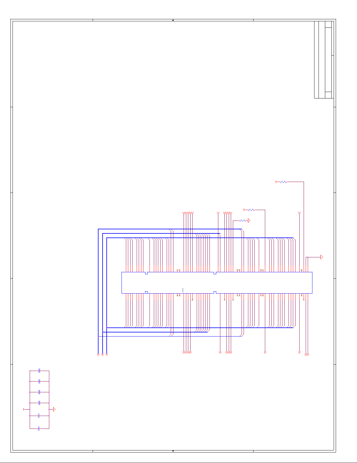
D
6 22Thursday, February 25, 1999
E
D
R125
4.7K
V3_3
R108
0
SCASB# 4
DQMA4 4,5,7
DQMA5 4,5
CS_A3# 4
SRASB# 4
CKE2 4
SDCLK5 8
V3_3
CS_B3# 4
DQMA6 4,5,7
DQMA7 4,5,7
R99
0
SDCLK7 8
Title
DIMM1
Size Document Number Rev
{Doc}
C
E
Date: Sheet of
D
THIS DRAWING CONTAINS INFORMATION WHICH HAS NOT
BEEN VERIFIED FOR MANUFACTURING AS AN END USER
PRODUCT. INTEL IS NOT RESPONSIBLE FOR THE
C
MD32
MD33
MD34
MD35
MD36
MD37
MD38
MD39
MD40
MD41
MD42
MD43
MD44
MD45
MD46
MD47
MECC4
MECC5
MAA1
MAA3
MAA5
MAA7
MAA9
MD50
MD51
MD52
MD53
MD54
MD49
MAA11
MAA13MAA12
MAA12
MECC6
MECC7
MD48
MD55
MD56
MD57
MD58
MD59
MD60
MD61
MD62
MD63
MISUSE OF THIS INFORMATION.
C
Slave address 10100001b
B85A01
B86
B87
B88
B89
B90
B91
B92
B93
B94
B95
B96
B97
B98
B99
B100
B101
B102
B103
B104
B105
B106
B107
B108
B109
B110
B111
B112
B113
B114
B115
B116
B117
B118
B119
B120
B121
B122
B123
B124
B125
B126
B127
B128
B129
B130
B131
B132
B133
B134
B135
B136
B137
B138
NC
/CAS
V3_3
DQMB4
DQMB5
V3_3
WE0
DQMB0
DQMB1
A26
A27
A28
A29
A1A3A5A7A9
/S1
BA0
GND
/RAS
/S0DUGNDA0A2A4A6A8A10(AP)
A30
A31
A32
A33
A34
A35
A36
A37
A38
A39
MAA0
MAA2
MAA4
MAA6
MAA8
MAA10
/S3
A11
A12
CK1
GND
V3_3
CKE0
DQMB6
V3_3
CK0
GNDDU/S2
V3_3
DQMB2
A41
A42
A43
A44
A45
A46
BA1
A40
GNDGND
DQ32
DQ33
DQ34
DQ35
DQ2
DQ3
DQ0
DQ1
J17
A02
A03
A04
A05
A06
B
MD3
MD1
MD0
MD2
V3_3
V3_3
GND
DQ36
DQ37
DQ38
DQ39
DQ40
DQ41
DQ8
GND
DQ4
A07
MD4
DQ9
DQ5
DQ6
DQ7
A08
A09
A10
A11
A12
A13
A14
MD6
MD7
MD8
MD5
MD10
MD9
DQ42
DQ10
A15
MD11
DQ43
DQ11
A16
MD12
DQ44
DQ12
A17
MD13
DQ45
DQ13
CB5
GND
V3_3
DQ46
DQ47
V3_3
DQ14
DQ15
CB0
CB1
GNDNCNC
A18
A19
A20
A21
A22
A23
A24
A25
MD15
MD14
MECC0
MECC1
NC
CB4
A13
V3_3
DQMB7
DQBM3DUV3_3NCNC
A47
A48
A49
B139
NC
NC
CB6
CB7
GND
DQ48
CB2
CB3
GND
DQ16
A50
A51
A52
A53
A54
A55
MD16
MECC2
MECC3
B140
A56
MD17
DQ49
DQ17
B141
DQ50
DQ18
A57
MD18
B142
A58
MD19
DQ51
DQ19
B143
V3_3
V3_3
A59
B144
B145
B146
B147
NC
DU
DQ52
REGE
DQ20NCVREF (NC)
CKE1
A60
A61
A62
A63
MD20
B148
GND
GND
A64
B149
A65
MD21
DQ53
DQ21
B150
A66
MD22
DQ54
DQ22
B151
A67
MD23
DQ55
DQ23
B152
A68
B157
B153
B154
B155
B156
B158
B159
B160
B161
B162
B163
B164
B165
B166
B167
B168
NC
SA0
SA1
SA2
DQ58
DQ26
MD27
CK3
GND
DQ62
DQ30
A77
MD31
DQ63
DQ31
V3_3
SDRAM DIMM
GND
CK2NCWP
SDA
SCL
V3_3
A78
A79
A80
A81
A82
A83
A84
B
V3_3
DQ59
DQ60
DQ61
DQ27
V3_3
DQ28
DQ29
A72
A73
A74
A75
A76
MD28
MD29
MD30
GND
DQ56
DQ57
GND
DQ24
DQ25
A69
A70
A71
MD26
MD25
MD24
Socket 1
WE_B#4
DQMA04,5,7
DQMA14,5
MD[63:0]4,5,7
MAA[13:0]4,5
C198
0.1uF
C183
0.1uF
C181
0.1uF
C182
0.1uF
A
V3_3
C103
47uF
MECC[7:0]4,5,7
CS_A2#4
CS_B2#4
DQMA24,5,7
DQMA34,5,7
SDCLK48
CKE34
SDCLK68
SMBDATA4,5,7,8,9,14
SMBCLK4,5,7,8,9,14
A
C104
47uF
4 4
3 3
2 2
1 1
Page 72
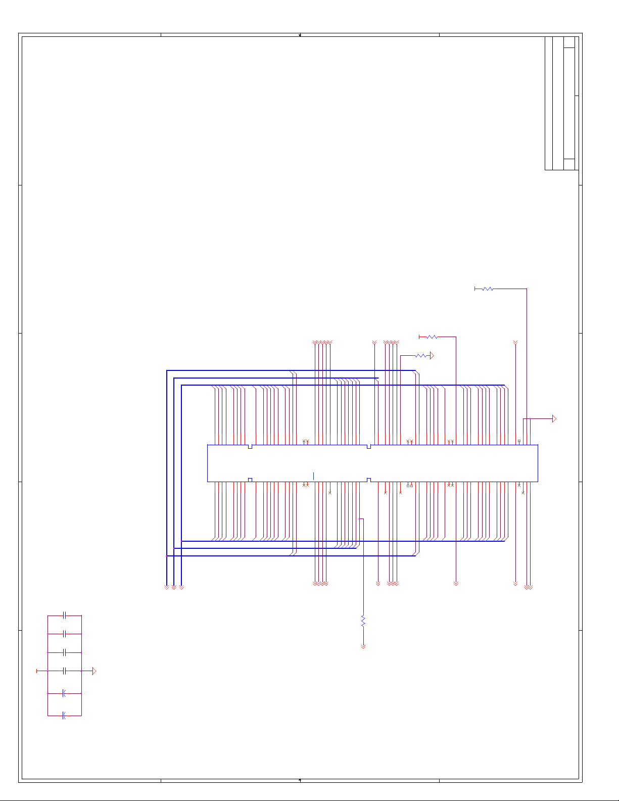
D
7 22Thursday, February 25, 1999
E
D
R126
4.7K
V3_3
R106
0
SCASA# 4,5
DQMA4 4,5,6
CS_A5# 4
SRASA# 4,5
MECC5
DQMB5 4
MAB#11MAB#10
MAB#9MAB#8
MAB#13
MAB#7MAB#6
MAB#5MAB#4
MAB#3
MAB#1
Note: J16 is not popula ted
MD35
MD37
MD38
MD32
MD36
MD33
C
MD34
MD39
MD40
MD41
MD42
MD43
MD44
MD45
MD46
MD47
MECC4
SDCLK9 8
MAB#12
CS_B5# 4
CKE4 4
DQMA6 4,5,6
R100
0
MD54
MD50
MD51
MD52
MD53
MD55
MD56
MD57
MD58
MECC6
MECC7
MD48
MD49
V3_3
DQMA7 4,5,6
MD59
MD60
MD61
MD62
MD63
SDCLK11 8
THIS DRAWING CONTAINS INFORMATION WHICH HAS NOT
Slave address 10100010b
DIMM2
Title
BEEN VERIFIED FOR MANUFACTURING AS AN END USER
PRODUCT. INTEL IS NOT RESPONSIBLE FOR THE
E
{Doc}
C
Size Document Number Rev
Date: Sheet of
D
MISUSE OF THIS INFORMATION.
C
B85A01
B86
B87
B88
B89
B90
B91
B92
B93
B94
B95
B96
B97
B98
B99
B100
B101
B102
B103
B104
B105
B106
B107
B108
B109
B110
B111
B112
B113
B114
B115
B116
B117
B118
B119
B120
B121
B122
B123
B124
B125
B126
B127
B128
B129
B130
B131
B132
B133
B134
B135
B136
B137
B138
NC
/CAS
V3_3
DQMB4
DQMB5
V3_3
WE0
DQMB0
DQMB1
A26
A27
A28
A29
DQMB14
WE_A#4,5
DQMA04,5,6
A1A3A5A7A9
/S1
BA0
GND
/RAS
/S0DUGNDA0A2A4A6A8A10(AP)
A30
A31
A32
A33
A34
A35
A36
A37
A38
MAB#2
MAB#0
CS_A4#4
A11
BA1
A39
A40
MAB#12
R97 10K
V3_3
V3_3
MAB#12_R8
/S3
A12
CK1
GND
CKE0
DQMB6
V3_3
CK0
GNDDU/S2
DQMB2
A41
A42
A43
A44
A45
A46
DQMA24,5,6
CS_B4#4
SDCLK88
GNDGND
DQ32
DQ33
DQ34
DQ35
DQ2
DQ3
DQ0
DQ1
J16
A02
A03
A04
A05
A06
MD3
MD1
MD2
MD0
B
C176
0.1uF
C174
0.1uF
C227
0.1uF
C197
C128
C156
0.1uF
47uF
47uf
V3_3
A
Socket 2
MECC[7:0]4,5,6
MAB#[13:0]4
MD[63:0]4,5,6
V3_3
V3_3
GND
DQ36
DQ37
DQ38
DQ39
DQ40
DQ41
DQ8
GND
DQ9
DQ4
DQ5
DQ6
DQ7
A07
A08
A09
A10
A11
A12
A13
A14
MD7
MD4
MD5
MD6
MD8
MD9
MD10
DQ42
DQ10
A15
MD11
DQ43
DQ11
A16
MD12
DQ44
DQ12
A17
MD13
DQ45
DQ13
CB5
GND
V3_3
DQ46
DQ47
V3_3
DQ14
DQ15
CB0
CB1
GNDNCNC
A18
A19
A20
A21
A22
A23
A24
A25
MD14
MECC1
MD15
MECC0
NC
CB4
A13
DQMB7
DQBM3DUV3_3NCNC
A47
A48
A49
DQMA34,5,6
V3_3
B139
NC
NC
CB6
CB7
GND
DQ48
CB2
CB3
GND
DQ16
A50
A51
A52
A53
A54
A55
MD16
MECC3
MECC2
B140
A56
MD17
DQ49
DQ17
B141
DQ50
DQ18
A57
MD18
B142
A58
MD19
B143
DQ51
DQ19
A59
B144
B145
B146
NC
DU
V3_3
DQ52
V3_3
DQ20NCVREF (NC)
A60
A61
A62
MD20
B147
A63
REGE
CKE1
CKE54
B148
GND
GND
A64
B149
A65
MD21
DQ53
DQ21
B150
A66
MD22
DQ54
DQ22
B151
A67
MD23
DQ55
DQ23
B152
A68
B157
B153
B154
B155
B156
B158
B159
B160
B161
B162
B163
B164
B165
B166
B167
B168
NC
SA0
SA1
SA2
DQ58
DQ26
A72
MD27
DQ59
DQ27
CK3
GND
DQ62
DQ30
A77
MD31
DQ63
DQ31
V3_3
SDRAM DIMM
GND
CK2NCWP
SDA
SCL
V3_3
A78
A79
A80
A81
A82
A83
A84
B
SDCLK108
SMBDATA4,5,6,8,9,14
SMBCLK4,5,6,8,9,14
A
V3_3
DQ60
DQ61
V3_3
DQ28
DQ29
A73
A74
A75
A76
MD28
MD30
MD29
GND
DQ56
DQ57
GND
DQ24
DQ25
A69
A70
A71
MD25
MD24
MD26
4 4
3 3
2 2
1 1
Page 73
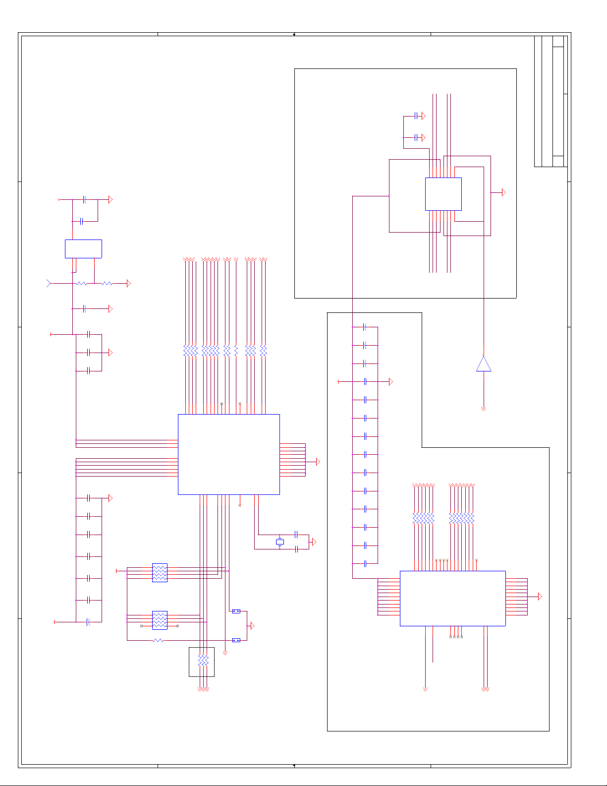
D
8 22Thursday, February 25, 1999
E
C94
V5_0
D
TP
1
TP17
V2.5
C
B
V3_3
A
10uF
C162
0.1uF
OutTab
R15
LT117
Adj/GND
1
Note: R11 and R12 should be placed as
124
1%
C95
100uF
C163
0.01uF
C164
0.01uF
C168
0.01uF
C170
0.01uF
C171
0.01uF
C101
0.01uF
C169
0.01uF
C173
0.01uF
C165
0.01uF
C93
47uF
close as possible to U1
R16
124
1%
V3_3
RP22
10K
RP20
10K
R20
2.7K
CPUCLK1 4
CPUCLK0 4
CPUCLK2 4
PCICLKF 14
PCICLK1 10
PCICLK2 10
PCICLK3 11
PCICLK4 3
PCLKAPIC 13
PCICLK7 4
USBCLK0 14
REF0 18
REF1 16
REF2 14
APICCLK0 13
APICCLK1 4
R24 33
R27 33
R29 33
R31 33
R23 33
R26 33
R28 33
R32 33
R30 33
R36 33
R34 33
R38 33
R18 33
R17 33
R19 33
R21 33
R22 33
CPUCLKR_0
CPUCLKR_1
CPUCLKR_2
CPUCLKR_3 CPUCLK3
PCICLKF_R
PCICLKR_1
PCICLKR_2
PCICLKR_3
PCICLKR_4
PCICLKR_6
PCICLKR_7
USBCLKR_0
REFR_0
REFR_1
REFR_2
APICCLKR_0
APICCLKR_1
1314161722
PCI_CLK4
PCI_CLK5
PCI_CLK6
PCI_CLK7
CY2280
SEL_SS#
SEL0
SEL1
SEL100
282726
25
12
12
MAB#12_R7
23
USBCLK0
USBCLK1
RESERVED
42
J14
HDR2
J15
JUMP2
1
2
47
45
44
REF0
REF1
REF2
APIC0
APIC1
XTALIN
XTALOUT
4
5
Y1
Keep crystal close to cl ock and
7
40
8433910361135
CPUCLK0
CPUCLK1
CPUCLK2
CPUCLK3
PCI_CLK1
PCI_CLK2
PCI_CLK3
PCICLK_F
VDDAPIC
46
VDDCPU
41
VDDCPU
37
AVDD
33
AVDDVSS
1920
VDDREF
48
VDDUSB
21
VDDPCI
9
VDDPCIVSS
153
U6
CPU_STOP#
PCI_STOP#
PWR_DWN#
30
31
29
4 5
3 6
2 7
1 8
4 5
3 6
2 7
1 8
R35 0
R33 0
R37 0
This circuit is only used for
TX/Pentium Designs. Note only
two DIMMS are supported.
VSS
VSS
38
VSS
34
VSS
32
VSS
24
VSS
18
VSS
12
VSS
6
C100
10pf
14.318MHz
C99
10pf
1 2
caps close to crystal. All lead
lengths should be equal.
V3_3
C148
C149
C150
C211
C216
C222
C224
C220
C225
C212
C221
C223
C217
C213
15uF
15uF
15uF
0.01uF
0.01uF
0.01uF
0.01uF
0.01uF
0.01uF
0.01uF
0.01uF
0.01uF
0.01uF
0.01uF
U5
Out In
2 3
4
V2.5
C209
10pF
C214
10pF
These caps can be tuned to
change delay through buffer.
SDCLK0 5
SDCLK1 5
R112 0
R110 0
SDCLKR0
SDCLKR1
46538109
VDD
46
VDD
42
VDD
37
SDRAM1
SDRAM0
VDD
33
VDD
29
VDD
23
VDD
20
VDD
VDD
VDD
VDD
U16
161
U26
CPUCLK3SDCLKR8
SDCLK2 5
SDCLK3 5
R119 0
R116 0
R114 0
SDCLKR2
SDCLKR3
1315147171918
SDRAM2
SDRAM3
CLK_IN
11
SDCLKR1
152
143
CLKA4CLKA1
CLKOUTRef
SDCLKR5
SDCLKR4
SDCLK8 7
SDCLK9 7
R121 0
SDCLKR9
SDRAM4
SDRAM5
OE
38
CONFIG1 SDCLKR0
134
125
VDDVDD
CLKA3CLKA2
31223212352636
SDRAM6
SDRAM7
SDCLKR3
SDCLKR2
116
107
GNDGND
CLKB4CLKB1
CLKB3CLKB2
SDCLKR6
SDCLKR7
SDCLK10 7
R120 0
SDCLKR10
SDRAM8
SDRAM9
SDRAM10
CY2318NZ
NCNCNC
1
98
S1S2
SDCLK11 7
R118 0
SDCLKR11
SDRAM11
2
Zero Delay Buffer
SDCLK4 6
SDCLK6 6
SDCLK7 6
R113 0
R111 0
R115 0
SDCLKR7
SDCLKR6
SDCLKR4
40274116443045
SDRAM12
SDRAM13
SDRAM14
NC
47
48
U21A
SDCLK5 6
BxFBCLK 4
R122 0
R109 0
SDCLKR5
213428
SDRAM15
SDRAM16
CONFIG1#
1 2
CONFIG14,14
SDRAM17
SDATA
24
25
SCLK
74HCT14
THIS DRAWING CONTAINS INFORMATION WHICH HAS NOT
VSS
43
VSS
39
VSS
VSS
VSS
VSS
VSS
VSS
VSS
VSS
VSS
Clocks
Title
BEEN VERIFIED FOR MANUFACTURING AS AN END USER
PRODUCT. INTEL IS NOT RESPONSIBLE FOR THE
E
{Doc}
C
Size Document Number Rev
Date: Sheet of
D
MISUSE OF THIS INFORMATION.
C
B
A
SMBDATA4,5,6,7,9,14
Stuff only to enable
stopping of clocks
CPU_STOP#14
PCI_STOP#14
SUSA#14
4 4
3 3
This circuit is only used for
BX/PentiumII Designs. Note
three DIMMS are supported.
2 2
BXDCLKO4
SMBCLK4,5,6,7,9,14
1 1
Page 74

D
9 22Thursday, February 25, 1999
E
D
V2.5
V5_0
RP50
2.7K
RP53
2.7K
RP49
2.7K
RP52
10K
RP25
1 8
2 7
3 6
4 5
1 8
2 7
3 6
4 5
1 8
2 7
3 6
4 5
1 8
2 7
3 6
PCI Pullups
C
4 5
2.7K
1 8
2 7
3 6
4 5
V3_3
R47 124
RP51
10K
1 8
2 7
3 6
4 5
R43 10K
R40 10K
R71 2.7K
R44 2.7K
R41 10K
RP38
R46 124
R45 1K
R49 1K
1 8
2 7
3 6
4 5
A20M#4,14
INIT4,14
APICD14,13
APICD04,13
CPURST4,14
IGNNE#4,14
V3_3
2.7K
RP40
2.7K
RP37
1 8
2 7
SLP#4,14
APICCS#13,14
3 6
4 5
SMBDATA4,5,6,7,8,14
SMBCLK4,5,6,7,8,14
2.7K
1 8
2 7
3 6
4 5
NMI4,14
INTR4,13,14
FERR#4,14
STPCLK#4,14
THIS DRAWING CONTAINS INFORMATION WHICH HAS NOT
ISA/PCI Pullups
Title
BEEN VERIFIED FOR MANUFACTURING AS AN END USER
Size Document Number Rev
PRODUCT. INTEL IS NOT RESPONSIBLE FOR THE
{Doc}
C
MISUSE OF THIS INFORMATION.
E
Date: Sheet of
D
C
-PLOCK3,4,10,11
-PREQ44
PAR3,4,10,11,13
-PERR3,10,11
-SERR3,4,10,11,13
-FRAME3,4,10,11,13
-IRDY3,4,10,11,13
-TRDY3,4,10,11,13
-DEVSEL3,4,10,11,13
-STOP3,4,10,11,13
PIRQB#3,10,11,12,13,14
PIRQD#3,10,11,13,14
PIRQC#3,10,11,12,13,14
-PREQ04,10,13
-PREQ14,10,13
1 8
SD12
2 7
SD13
3 6
SD14
4 5
SD15
-PREQ24,11,13
-PREQ33,4,13
SDONE10,11
-SBO10,11
REQ64#10,11
ACK64#10,11
10K
RP19
1 8
2 7
3 6
4 5
SA0
SA1
SA2
SA3
PIRQA#3,10,11,13,14
B
V5_0
RP9
10K
RP8
10K
RP33
10K
1 8
2 7
3 6
4 5
1 8
2 7
3 6
ISA Pullups
SD0
A
SD1
4 5
SD2
SD3
SD4
SD5
SD6
SD7
RP35
1 8
2 7
3 6
4 5
SD9
SD10
SD11
SD8
-PHOLD4,13
-PHOLDA4,13
-PGNT04,10
-PGNT14,10
-PGNT24,11
-PGNT33,4
-PGNT44
RP29
10K
RP10
1K
RP23
1K
RP21
1 8
2 7
3 6
4 5
1 8
2 7
3 6
4 5
1 8
2 7
3 6
4 5
MEMR#13,18,20
IOR#13,16,18
REFRESH#13,18
MEMW#13,18,20
IOW#13,16,18,20
10K
RP17
10K
RP15
10K
RP13
10K
RP11
10K
RP27
10K
RP24
1 8
2 7
3 6
4 5
1 8
2 7
3 6
4 5
1 8
2 7
3 6
4 5
1 8
2 7
3 6
4 5
1 8
2 7
3 6
4 5
SA4
SA5
SA6
SA7
SA8
SA9
SA10
SA11
SA12
SA13
SA14
SA15
SA16
SA17
SA18
SA19
LA17
LA18
LA19
LA20
1 8
LA21
2 7
LA22
3 6
LA23
10K
4 5
MASTER16#18
RP16
IOCHRDY13,16,18
ZEROWS#13,18
1 8
2 7
IOCS16#13,18
MEMCS16#13,18
IOCHK#13,18
10K
RP14
3 6
4 5
1 8
2 7
3 6
4 5
10K
1 8
2 7
3 6
4 5
SMEMW#13,18
SMEMR#13,18
SBHE#13,18
BALE13,18
10K
RP26
10K
RP12
5.6K
RP34
1 8
2 7
3 6
4 5
1 8
2 7
3 6
4 5
5.6K
1 8
2 7
3 6
4 5
B
A
IRQ113,14,16
IRQ313,14,16,18
IRQ413,14,16,18
IRQ513,14,16,18
IRQ613,14,16,18
IRQ713,14,16,18
IRQ913,14,18
IRQ1013,14,16,18
IRQ1113,14,18
IRQ1213,14,16,18
IRQ1413,14,15,16,18
IRQ1513,14,15,16,18
DRQ014,16,18
DRQ114,16,18
DRQ214,16,18
DRQ314,16,18
DRQ514,18
DRQ614,18
DRQ714,18
LA[23:17]13,18
SD[15:0]13,16,18,20
4 4
SA[19:0]13,16,18,20
3 3
Note IRQ8 Pull-up
is on PIIX4 page
2 2
1 1
Page 75

D
10 22Thursday, February 25, 1999
R13
V5_0
CLK
A17B3A18
B17
220
PCIB2
AD29
-PGNT1 4,9
AD18
AD22
AD24
AD26
B21
AD29
AD28
A22
V3_3
AD[29]
B22
A23
A24
AD[28]NCAD[26]
GND
AD[27]
B23
B24
AD25
AD27
A25
GND
AD[25]
B25
-C/BE3
A26
AD[24]
V3_3
B26
A27
IDSEL
C/BE3
B27
AD23
A28
V3_3
AD[23]
B28
AD20
A29
AD[22]
GND
B29
AD21
A30
AD[20]
AD[21]
B30
AD19
A31
GND
AD[19]
B31
AD[18]
V3_3
AD30
A19
A20B4A21
NC
GNT
GND
AD[30]
GND
REQ
V5_0
AD[31]
B18
B19
B20
AD31
AD16
A32
B32
AD17
A33
AD[16]
AD[17]
B33
-C/BE2
-FRAME
A34
V3_3
C/BE2
B34
A35
FRAME
GND
B35
GND
IRDY
-TRDY
A36
TRDY
V3_3
B36
-STOP
A37
A38
A39
GND
V3_3
STOP
DEVSEL
GND
LOCK
B37
B38
B39B5B40B6B41B7B42B8B43B9B44
SDONE
-SBO
A40
A41
SDONE
PERR
SBO
V3_3
PAR
AD13
AD6
AD11
A47
B47
AD12
A48
AD[11]
AD[12]
B48
AD10
AD9
A49
GND
AD[10]
B49
AD[09]
GND
A52
B52
AD8
A53
C/BE0
AD[08]
B53
AD7
A54
V3_3
AD[07]
B54
AD4
A55
AD[06]
V3_3
B55
AD5
A56
AD[04]
AD[05]
B56
AD3
AD2
A57B57
GND
AD[03]
AD0
A58
A59
A60
A61
A62
V5_0
V5_0
V5_0
AD[02]GND
AD[00]
REQ64
PCI SLOT 1
PCI Conn
ACK64
V5_0
V5_0
V5_0
AD[01]
B60
B61
B62
B58
B59
AD1
ACK64# REQ64#
-C/BE0
AD15
A42
A43
A44
A45
A46
PAR
GND
V3_3
AD[13]
AD[15]
AD[14]
GND
SERR
V3_3
C/BE1
B45
B46
AD14
-C/BE1
PCI Slots 0 & 1
{Doc}
C
Title
Size Document Number Rev
Date: Sheet of
E
D
E
D
C107
C91
C120
C67
C74
C86
C114
C117
C56
0.1uF
0.1uF
10uF
0.01uF
0.01uF
0.1uF
0.1uF
0.1uF
10uF
J8
PCI_TRST
PCI_TMS
A2B1A3
+12V
TRST
-12V
TCK
PCI_TCLK
PCI_TDI
A4
TMS
GND
-PCIRST
PIRQD#
PIRQB#
A8A1A9
A10
A5
A6
A7
A11
A12
A13B2A14
A15
A16
NC
NC
INTA
V5_0
PIRQA#
INTC
INTB
PIRQC#
V5_0
INTD
V5_0
PRSNT1
B10
B11
GND
PRSNT2
GND
B12
C81
0.01uF
NC
RST
GND
GND
NC
GND
B13
B14
B15
B16
TDI
V5_0
TDO
V5_0
C78
0.01uF
-PREQ14,9,13
PCICLK28
R12
-PGNT0 4,9
A17B3A18
GNT
V5_0
GND
CLK
B17
B18
PCICLK1
A19
GND
REQ
B19
-PREQ04,9,13
NC
V5_0
AD28
AD30
A20B4A21
AD[30]
AD[31]
B20
AD31
B21
AD29
AD28
A22
V3_3
AD[29]
B22
AD26
A23
AD[28]
GND
B23
AD27
A24
AD[26]
AD[27]
B24
AD25
220
GND
AD[25]
PCIA2
AD24
A25
AD[24]
V3_3
B25
-C/BE3
A26
IDSEL
C/BE3
B26
C
B
C90
0.1uF
C106
C119
C66
C113
C73
C85
C116
C55
0.1uF
10uF
0.01uF
0.01uF
0.1uF
0.1uF
0.1uF
10uF
AD[31:0]
AD[31:0]3,4,11,13
-C/BE[3:0]
-C/BE[3:0]3,4,11,13
V3_3V5_0 V3_3V5_0
PIRQA# 3,9,11,13,14
PCI_TDI 11
PCI_TMS 11
PCI_TRST 11
A2B1A3
A4
A5
A6
A7
TDI
TMS
INTA
+12V
V5_0
TRST
J7
-12V
TCK
TDO
GND
V5_0
V5_0
PCI_TCLK11
PIRQC# 3,9,11,12,13,14
A8A1A9
A10
A11
A12
NC
NC
INTC
V5_0
V5_0
PRSNT2
NC
INTB
INTD
PRSNT1
B10
B11
B12
PIRQD#3,9,11,13,14
PIRQB#3,9,11,12,13,14
GND
GND
A13B2A14
B13
GND
GND
B14
-PCIRST 3,4,11,12,13
A15
A16
NC
RST
GND
NC
B15
B16
A27
B27
AD23
AD22
A28
V3_3
AD[23]
B28
AD20
A29
AD[22]
GND
B29
AD21
A30
AD[20]
AD[21]
B30
AD19
AD18
A31
GND
AD[19]
B31
AD16
A32
AD[18]
V3_3
B32
AD17
A33
AD[16]
AD[17]
B33
-C/BE2
-IRDY
-FRAME 3,4,9,11,13
A34
A35
V3_3
FRAME
GND
C/BE2
B34
B35
-DEVSEL
-TRDY 3,4,9,11,13
A36
A37
A38
GND
GND
TRDY
V3_3
DEVSEL
IRDY
B36
B37
B38
-IRDY3,4,9,11,13
-DEVSEL3,4,9,11,13
-PLOCK
-PERR
-SERR
-STOP 3,4,9,11,13
SDONE 9,11
-SBO 9,11
PAR 3,4,9,11,13
A39
A40
A41
A42
SBO
GND
V3_3
STOP
SDONE
LOCK
GND
PERR
V3_3
SERR
B39B5B40B6B41B7B42B8B43B9B44
-PLOCK3,4,9,11
-PERR3,9,11
-SERR3,4,9,11,13
A43
PAR
V3_3
-C/BE1
AD15
A44
A45
AD[15]
C/BE1
B45
AD14
AD13
A46
V3_3
AD[14]
B46
AD11
A47
AD[13]
GND
B47
AD12
A48
AD[11]
AD[12]
B48
AD10
AD9
A49
GND
AD[10]
B49
AD[09]
GND
A52
B52
AD8
A53
C/BE0
AD[08]
B53
AD7
AD6
A54
V3_3
AD[07]
B54
AD4
A55
AD[06]
V3_3
B55
AD5
A56
AD[04]
AD[05]
B56
AD3
AD2
A57B57
GND
AD[03]
THIS DRAWING CONTAINS INFORMATION WHICH HAS NOT
BEEN VERIFIED FOR MANUFACTURING AS AN END USER
PRODUCT. INTEL IS NOT RESPONSIBLE FOR THE
MISUSE OF THIS INFORMATION.
C
REQ64# 9,11
AD0
A58
A59
A60
A61
A62
V5_0
V5_0
V5_0
AD[00]
AD[02]GND
REQ64
PCI SLOT 0
PCI Conn
ACK64
V5_0
V5_0
V5_0
AD[01]
B60
B61
B62
B58
B59
AD1
-C/BE0
ACK64#9,11
B
A
J7/J8 V5_0:
A5, A8, A10, A16, A59, A61, A62 | A1, A3, A4
B5, B6, B19, B22, B59, B61, B62
J7/J8 V3_3:
A21, A27, A33, A39 A45, A53
B25, B31, B36, B41, B43, B54
J7/J8 NC:
A9, A11, A1 4, A19
B10, B14
J7/J8 GND:
A12, A13, A18, A24, A30, A35, A37, A42, A48, A56
4 4
B3, B12, B13, B15, B17, B28, B34, B38, B46, B49,
B57
J7/J8 +12V: A2
-12V: B1
PCICLK18
C80
0.01uF
C77
0.01uF
3 3
2 2
1 1
A
Page 76

D
11 22Thursday, February 25, 1999
E
R67
4.7K
D
R66
R68
V5_0
C
4.7K
R69
4.7K
4.7K
PCI_TRST
PCI_TDI PCI_TMS PCI_TCLK
THIS DRAWING CONTAINS INFORMATION WHICH HAS NOT
PCI Slot 2
Title
BEEN VERIFIED FOR MANUFACTURING AS AN END USER
PRODUCT. INTEL IS NOT RESPONSIBLE FOR THE
E
{Doc}
C
Size Document Number Rev
Date: Sheet of
D
MISUSE OF THIS INFORMATION.
C
R14
220
PCIC2
AD30
-PCIRST 3,4,10,12,13
A10
A11
NC
V5_0
PRSNT1
B10
B11
A12
NC
GND
PRSNT2
GND
B12
C82
A13B2A14
GND
GND
B13
-PGNT2 4,9
AD26
AD24
AD30
AD28
A15
A16
A17B3A18
A19
A20B4A21
A22
A23
A24
A25
NC
RST
GNT
V5_0
NC
GND
CLK
GND
B14
B15
B16
B17
PCICLK38
0.01uF
A26
NC
GND
GND
V3_3
AD[28]NCAD[26]
AD[24]
AD[30]
REQ
V5_0
AD[31]
AD[29]
GND
AD[27]
AD[25]
V3_3
B18
B19
B20
B21
B22
B23
B24
B25
B26
AD31
AD25
AD29
AD27
-C/BE3
-PREQ24,9,13
PIRQC# 3,9,10,12,13,14
PIRQA# 3,9,10,13,14
PCI_TDI 10
PCI_TMS 10
PCI_TRST 10
C92
0.1uF
C108
C121
C115
C68
C118
C75
C87
C57
0.1uF
10uF
0.01uF
0.01uF
0.1uF
0.1uF
0.1uF
10uF
AD[31:0]
AD[31:0]3,4,10,13
-C/BE[3:0]
-C/BE[3:0]3,4,10,13
A8A1A9
A2B1A3
A4
A5
A6
A7
TDI
TMS
INTA
INTC
+12V
V5_0
V5_0
TRST
J9
-12V
TCK
GND
TDO
V5_0
V5_0
INTB
INTD
PIRQB#3,9,10,12,13,14
PIRQD#3,9,10,13,14
PCI_TCLK10
V3_3V5_0
B
A
IDSEL
C/BE3
AD23
A27
B27
AD22
A28
V3_3
AD[23]
B28
AD20
A29
AD[22]
GND
B29
AD21
A30
AD[20]
AD[21]
B30
AD19
AD18
A31
GND
AD[19]
B31
AD16
A32
AD[18]
V3_3
B32
AD17
A33
AD[16]
AD[17]
B33
-C/BE2
-FRAME 3,4,9,10,13
A34
A35
V3_3
FRAME
GND
C/BE2
B34
B35
-TRDY 3,4,9,10,13
A36
A37
A38
GND
GND
TRDY
V3_3
DEVSEL
IRDY
B36
B37
B38
-IRDY3,4,9,10,13
-DEVSEL3,4,9,10,13
-STOP 3,4,9,10,13
SDONE 9,10
-SBO 9,10
PAR 3,4,9,10,13
A39
A40
A41
A42
SBO
GND
V3_3
STOP
SDONE
GND
LOCK
PERR
V3_3
SERR
B39B5B40B6B41B7B42B8B43B9B44
-PLOCK3,4,9,10
-PERR3,9,10
-SERR3,4,9,10,13
A43
PAR
V3_3
-C/BE1
AD15
A44
A45
AD[15]
C/BE1
B45
AD14
AD13
A46
V3_3
AD[14]
B46
AD11
A47
AD[13]
GND
B47
AD12
A48
AD[11]
AD[12]
B48
AD10
AD9
A49
GND
AD[10]
B49
AD[09]
GND
REQ64# 9,10
AD4
AD2
AD0
AD6
A52
A53
A54
A55
A56
A57B57
A58
A59
A60
A61
A62
GND
V5_0
AD[06]
V3_3
B55
AD5
AD[04]
AD[05]
B56
AD3
AD[03]
V5_0
V5_0
AD[02]GND
AD[00]
REQ64
B
A
B58
AD1
AD[01]
B59
V5_0
B60
ACK64
B61
ACK64#9,10
V5_0
PCI SLOT 2
PCI Conn
V5_0
B62
-C/BE0
V3_3
C/BE0
AD[08]
AD[07]
B52
B53
B54
AD7
AD8
C79
0.01uF
4 4
3 3
2 2
1 1
Page 77

D
12 22Thursday, February 25, 1999
V5_0V5_0
R65
4.7K
A1B1
A3
12VOVRCNT#
SPARE
RESERVED
U2B
3 4147
A4
A5
A6
GND
USB-
PIRQB# 3,9,10,11,13,14
74AS07
GST1 4
GGNT# 4
-PCIRST 3,4,10,11,13
A7
A8
A9
A10
A11
ST1
3.3V
RST#
GNT#
INTA#
GPIPE# 4
A12
A13
A14
GND
PIPE#
RESERVED
SBA1
A15
SPARE
SBA1
A16
SBA3
A17
3.3V
A18
A19
SBA3
RESERVED
E
AGP Connector
C
Title
Size Document Number Rev
Date: Sheet of
GPAR 4
GPME# 14
GSTOP# 4
GTRDY# 4
GFRAME# 4
D
SBA7
SBA5
GAD30
GAD28
GAD26
GAD24
GAD22
GAD20
GAD18
GAD16
GC/BE#3
A26B26
A28
A29
A30
A31
A32
A33
A34
A35
A36
A37
A38
A39
A40
A41
AD22
VDDQ3.3
AD20
A42
NC
GND
AD18
AD16
FRAME#
VDDQ3.3
A20
A21
3.3V
AD30AD31
AD26
AD24
GND
RESERVED
C/BE3#
GND
SBA5
SBA7
GAD15
GAD13
GAD11
GAD9
GAD6
GAD4
GAD2
GAD0GAD1
GC/BE#0
A43
A44
A45
A46
A47
A48
A49
A50
A51
A52
A53
A54
A55
A56
A57
A58
A59
A60
A61
A62
A63
A64
A65
NC
3.3V
GND
TRDY#
STOP#
PME#
AD9
PAR
GND
GND
AD15
AD13
AD11
C/BE0#
VDDQ3.3
3.3V
RESERVED
A66
AD6
AD4
AD2
AD0
GND
SMB1
VDDQ3.3
AGP Connector
E
C180
0.01uF
C172
0.01uF
C177
0.01uF
C167
0.01uF
C166
0.01uF
D
C178
V3_3
C179
C184
C185
C186
0.01uF
0.01uF
0.01uF
0.01uF
0.01uF
V3_3
Pin A3 is tied to ground per AGP Specification
Rev 1.0
+12V
J13
5.0V
5.0V
USB+
GND
INTB#
CLK
REQ#
3.3V
ST0
ST2
RBF#
GND
SPARE
SBA0
3.3V
SBA2
B2
B3
B4
B5
B6
B7
B8
C
V5_0
V3_3 V3_3
B
SBA[7:0]4
V3_3
B9
B10
GCLK4
GREQ#4
R64
4.7K
12147
U2A
74AS07
PIRQC#3,9,10,11,13,14
SB_STB
B11
B12
B13
B14
B15
B16
B17
B18
B19
SBA2
SBA0
GSB_STB4
GST24
GRBF#4
GST04
AD29 AD28
3.3V
AD27
AD25
GND
AD_STB1
AD23
VDDQ3.3
AD21
AD19
GND
AD17
C/BE2#
VDDQ3.3
IRDY#
SPARE
GND
SPARE
3.3V
DEVSEL#
VDDQ3.3
PERR#
GND
SERR#
C/BE1#
VDDQ3.3
AD14
AD12
GND
SBA4
SBA6
B27 A27A2B28
B29
B30
B31
B32
B33
B34
B35
B36
B37
B38
B39
B40
B41
B42
B43
B44
B45
B46
GC/BE#2
B47
GIRDY#4
GDEVSEL#4
V3_3
SBA4
B20
B21
GAD17
GAD19
GAD21
GAD23
GAD25
GAD27
GAD29
GAD31
SBA6
GAD_STB14
V3_3
GND
AD10
AD8
VDDQ3.3
AD_STB0
AD7
GND
AD5
AD3
VDDQ3.3
AD1
SMB0
B48
B49
B50
B51
B52
B53
B54
B55
B56
B57
B58
B59
B60
B61
B62
B63
B64
B65
B66
GAD3
GAD5
GAD7
GAD8
GAD10
GAD12
GAD14
GC/BE#1
R83 8.2K
R85 8.2K
GAD_STB04
V3.3SUS
GAD[31:0]4
THIS DRAWING CONTAINS INFORMATION WHICH HAS NOT
BEEN VERIFIED FOR MANUFACTURING AS AN END USER
PRODUCT. INTEL IS NOT RESPONSIBLE FOR THE
MISUSE OF THIS INFORMATION.
C
GC/BE#[3:0]4
B
A
R87 8.2K
R77 8.2K
R76 8.2K
R78 8.2K
R79 8.2K
R80 8.2K
R82 8.2K
R81 8.2K
R72 8.2K
R73 8.2K
R74 8.2K
R86 8.2K
R75 8.2K
R84 8.2K
GAD_STB0
GAD_STB1
GSB_STB
GFRAME#
GIRDY#
GTRDY#
GSTOP#
GDEVSEL#
GREQ#
GGNT#
GPIPE#
GRBF#
GPAR
GPME#
Stub length from connector to resistor
must be less than 0.1"
4 4
3 3
2 2
1 1
A
Page 78

D
V2.5
APICD0 4,9
APICD1 4,9
APICCLK0 8
C210
E
RSTDRV# 15
Note: U14, C203,C215, C210 , R50
and R51 are not popula ted
XD0
XD1
XD2
XD3
XD4
XD5
XD6
XD7
U21B
XD[7:0] 20
74HCT14
3 4
0.1uF
C215
0.1uF
5
APICD0
C203
0.1uF
V5_0
APICD1
APICCLK
VCC
VCC
VCC
U14
IRQ7 9,14,16,18
IRQ6 9,14,16,18
IRQ5 9,14,16,18
IRQ4 9,14,16,18
IRQ0 14
IRQ1 9,14,16
INTR 4,9,14
IRQ3 9,14,16,18
IRQ8_Buf
3559255826572756285529543153305024152313221416121811216137938103984024160426243446
INTIN0
INTIN1
INTIN2D0INTIN3D1INTIN4D2INTIN5D3INTIN6D4INTIN7D5INTIN8D6INTIN9
D7
D/I#
RD#
WR#
IRQ10 9,14,16,18
IRQ9 9,14,18
INTIN10
CS#
IRQ12 9,14,16,18
IRQ11 9,14,18
IRQ14 9,14,15,16,18
I13R
INTIN11A0INTIN12A1INTIN13
INTIN14
APICREQ#
APICACK1#
APICACK2#
PIRQA# 3,9,10,11,14
PIRQB# 3,9,10,11,12,14
IRQ15 9,14,15,16,18
INTIN15
INTIN16
INTIN17
PCICLK
RESET
PIRQC# 3,9,10,11,12,14
PIRQD# 3,9,10,11,14
IRQ9OUT# 14
INTIN18
INTIN19
INTIN20
TESTIN#
3
I21R
I22R
INTIN21
INTIN22
NC
7
206432333617455246194744851493463
PX4_SMI# 14
SMIOUT#
INTIN23/SMI#
NC
NC
NC
NC
NC
J23
123
NC
NC
NC
SMI# 4
JUMP3
R50 1K
R51 1K
GND
GND
GND
1
NC
82093AA
IRQ8_Buf
PIIX4 Part 1
{Doc}
C
Title
Size Document Number Rev
13 22Thursday, February 25, 1999
E
Date: Sheet of
D
RSTDRV
18171615141312
11
B1B2B3B4B5B6B7
B8
A1A2A3A4A5A6A7A8G
U7
2345678
SDD15
D15
SDD14
SDD15
C18
SDCS3# 15
H16
DS3S#
PDCS3# 15
B18
DS3P#
SDCS1# 15
H17
DS1S#
PDCS1# 15
DS1P#
SA[19:0] 9,16,18,20
SA0
SA1
U11
T11
SA0
SA1
SA2
W11
Y11
T10
SA2
SA3
SA4
SA13
W10
Y9
T8
W8
U7
V7
Y7
SA5
SA6
SA7
SA8
SA9
SA10
SA11
SA12
SA12
SA6
SA9
SA5
SA8
SA11
SA7
SA10
SA4
SA3
SDD[15:0] 15
C
SDD0
E15
SDD1
SDD0
SDD2
SDD3
SDD4
SDD5
SDD6
SDD7
SDD8
SDD9
SDD10
SDD11
SDD12
SDD13
SDD14
B15
D14
C14
A14
C13
A13
C12
D12
B13V4D13
B14D9E14
A15
C15
SDD1
SDD2
SDD3
SDD4
SDD5
SDD6
SDD7
SDD8
SDD9
SDD10
SDD11
SDD12
SDD13
IDE
SIGNALS
SA13
SA14
SD[15:0] 9,16,18,20
SD0
SD1
SD2
SD0
SD1
SD2
SA18
SA17
SA16
SA19
SA15
V6
Y6
SA14
SA15
W3
T5
W5
U4
SD1
SA16
SA17
SA18
SA19
SD3
SD4
SD3
SD4
T2
W2
SD2
SD3
9191
SD5
SD6
SD7
SD5
SD6
SD7
SD8
Y2
T1
V1
W16
SD4
SD5
SD6
SD7
ISA/EIO
DIR
74ALS245
XOE#14
XDIR#14
SD9
SD10
SD11
SD12
SD13
T16
Y17
V17
Y18U9W18
SD8
SD9
SD10
SD11
SD12
SD13
SIGNALS
SD14
Y19V9W19
SD14
SD15
LA[23:17] 9,18
SD15
LA17
LA18
LA19
Y15
T14
W14
GPO1/LA17
GPO2/LA18
LA20
LA21
LA22
U13
V13U2Y13
GPO3/LA19
GPO4/LA20
GPO5/LA21
LA23
T12
GPO6/LA22
GPO7/LA23
MEMCS16# 9,18
MEMR# 9,18,20
MEMW# 9,18,20
SMEMR# 9,18
Y12
V15
U15W4U3T7U10Y1W7
MEMR#
MEMW#
SMEMR#
MEMCS16#
SA4
SA0
SMEMW# 9,18
SYSCLK 18
BALE 9,18
SYSCLK
SMEMW#
GPO0/BALE
SA1
MEMR#
IOCHK# 9,18
GPI0/IOCHK#
MEMW#
APICCS#9,14
APICREQ#14
APICACK1#14
REFRESH# 9,18
IOCS16# 9,18
ZEROWS# 9,18
SBHE# 9,18
V12Y3W12W1Y5T4T3
SBHE#
IOCS16#
ZEROWS#
REFRESH#
WSC#4
RSTDRV 16,18
IOR# 9,16,18
IOR#
RSTDRV
RSTDRV
PCLKAPIC8
IOW# 9,16,18,20
IOCHRDY 9,16,18
AEN 16,18,20
Y4
AEN
IOW#
IOCHRDY
V5_0
RP59
182736
I13R
I21R
I22R
45
10K
RSTDRV
D4
Bat54
1
3 1
2
R117 10K
V3.3SUS
This circuit is to prevent IOAPIC
from being powered by IRQ#8
U15A
74LVC125
2 3
7
14
IRQ#814
when in suspend and power
is not applied to device.
THIS DRAWING CONTAINS INFORMATION WHICH HAS NOT
BEEN VERIFIED FOR MANUFACTURING AS AN END USER
PRODUCT. INTEL IS NOT RESPONSIBLE FOR THE
MISUSE OF THIS INFORMATION.
D
C
PIIX4
B
U8A
AD0
AD1
AD2
AD3
AD4
AD5
AD6
AD7
AD8
AD9
AD10
AD11
AD12
A9
B8
C9
B10
A10
AD0
AD1
AD2
AD3
A
AD[31:0]3,4,10,11
B7
C7
AD4
AD5
AD6
AD7
AD8
AD9
AD10
AD11
AD12
4 4
A7D6E6
AD13
AD13
AD14
AD14
AD15
AD15
E4C4B4
AD16
AD16
AD17
AD17
AD18
A4D3E3C3B3
AD18
AD19
AD18
AD19
AD20
PCI
AD20
AD21
AD21
AD22
SIGNALS
AD22
AD23
AD24
AD25
AD26
AD27
E2C2B2
A2D1E1C1B1
AD23
AD24
AD25
AD26
AD27
AD28
AD28
AD29
R39
AD29
AD30
C/BE#0
C/BE#1
C/BE#2
C/BE#3
CLOCKRUN#
DEVSEL#
FRAME#
IDSEL
IRDY#
PAR
PCIRST# SD0
PHOLD#
PHOLDA#
SERR#
STOP#
TRDY#
PDD0
PDD1
PDD2
PDD3
PDD4
PDD5
PDD6
PDD7
PDD8
PDD9
PDD10
PDD11
C20
PDD5
B20
PDD6
A20
PDD7
A19B9B19
PDD8
PDD9
C19D8D19E8D17
PDD10
PDD11
PDD12
PDD12
E19A8E17D7F19
PDD13
AD30
AD31
AD31
220
C8
C6
-C/BE0
-C/BE1
-C/BE[3:0]3,4,10,11
D4
D2
-C/BE2
-C/BE3
PIIX4 is PCI
E5
A5
A3
B5
C10
CLKRUN#3,4
-DEVSEL3,4,9,10,11
-FRAME3,4,9,10,11
R_AD18
device #8
-IRDY3,4,9,10,11
3 3
A1 V3
B12
A12
PAR3,4,9,10,11
-PHOLD4,9
-PCIRST
3,4,10,11,12
D5
-SERR3,4,9,10,11
-PHOLDA4,9
C229
Place near PIIX4
C5
E10
-STOP3,4,9,10,11
-TRDY3,4,9,10,11
47pF
REQ0#
A11
-PREQ04,9,10
REQ1#
B11
-PREQ14,9,10
REQ2#
C11
-PREQ24,9,11
REQ3#
-PREQ33,4,9
F20
E18
E20
D18
D20
PDD0
PDD1
PDD2
PDD3
PDD4
PDD[15:0]15
PDD13
PDD14
PDD14
PDD15
PDD15
IDE
PDDACK#
SDA0
SDA1
SDA2
B17B6A16
A18A6F16
C17
G19
SDA015
SDA115
SDA215
PDDACK#15
SIGNALS
SDDACK#
PDREQ#
SDREQ#
PDIOR#
PDIOW#
A17
F18
F17
G20
SDDACK#15
PDREQ15
SDREQ15
PDIOR#15
PDIOW#15
2 2
PIORDY
SDIOR#
C16
PIORDY15
SDIOR#15
SDIOW#
B16
SDIOW#15
SIORDY
D16
SIORDY15
PIIX4E
PDA0
PDA1
PDA2
G16
G18
G17
PDA015
PDA115
PDA215
1 1
B
A
Page 79

D
V3_3
V3.3SUS
E
PWRON# 21
U24E
OC1# 17
J2
OC1#
DREQ1
TP11
TP
EXTSMI#
V20
EXTSMI#
DREQ2
DREQ3
11 10
14
1
SUSA# 8
W20
V19
U18
SUSA#
GPO15/SUSB#
GPO16/SUSC#
DREQ5
DREQ6
DREQ7
Y16
U16
U17
74LCT14
7
TP
TP13
PCI_STOP# 8
CPU_STOP# 8
ZZ 4
SUS_STAT1# 4
R2
K16
T17
GPO19/ZZ
GPO18/PCI_STP#
GPO17/CPU_STP#
GPO20/SUS_STAT1#
POWER
MGMT.
REQA#/GPI2
REQB#/GPI3
REQC#/GPI4
GNTA#/GPO9
GNTB#/GPO10
N2P3N1P2P4
M1
T18
GPO21/SUS_STAT2#
GNTC#/GPO11TCAPICACK#/GPO12
V3.3SUS
D
USBP1+ 17
OC0# 17
USBP0+ 17
USBP1- 17
USBP0- 17
F1H2G2H3J1
V3.3SUS
C194
0.1uF
R16
N16
K5
E9
C
C189
C190
C192
C187
E12
F5L12
F14
G6
R7
P15
T6
F6
E11
F15
R6
0.1uF
0.1uF
U8B
0.1uF
0.1uF
U14
OC0#
USBP1-
USBP0-
USBP1+
USBP0+
VCCSUS
VCCSUS
VCCSUSB
VCCP
USB
SIGNALS
VCCP
VCCPVSS
VCCP
VCCP
VCCP
VCCP
VCCP
VCC
VCC
VCC
VCC
DACK0#
DACK1#
DACK2#
DACK3#
DACK5#
DACK6#
DACK7#
DREQ0
V5
Y10
T15
V16
W17
W15
1
RSMRST# 21
THERM#
BATLOW#
H19
U19
M17
RSMRST#
GPI8/HCT#
GPI9/BATLOW#
DMA/IRQ
J17
V10
SMBDATA 4,5,6,7,8,9
SMBCLK 4,5,6,7,8,9
PWRBTN# 21
LID
SMBALERT#
U20
P16U6T20
R19
N17J20
SMBCLK
PWRBT#
GPI10/LID
SMBDATA
GPI11/SMBALERT#IRQ1
SIGNALS
IRQ0/GP014
APICCS#/GPO13
APICREQ#/GP15
H20
H18
K18
RP39 10K
1 8
2 7
THERM#
SERIRQ
GPME# 12
P18
GPI12/RI#A
IRQ3
IRQ4
T9
U8U5V8
IRQ5
3 6
LID
IRQ6
4 5
EXTSMI#
V5_0
IRQ7
IRQ8/GPI6
Y8
Y20
IRQ9
U1
U12
RP36 10K
1 8
SMBALERT#
V3_3
D3
R42
1K
PIIX4
IRQ10
IRQ11
IRQ12
T13
V14
W13
2
Bat54
IRQ14
TEST#
2 7
IRQ15
Y14
3 6
CONFIG2
4 5
IRQ#8
V3.3SUS
31
C134
C129
J16
VREF
SERIRG/GPI7
PIRQA#
PIRQB#
P5
R3
R4
J19
10uF
0.1uF
PIRQC#
G1
PIRQD#
K20
RP31 10K
SLP#
M19
1 8
CPURST
FERR#
K19
2 7
P19
GPI1
IGNNE#
L17
182736
45
RP28 10K
RP32
GPI21
SYSTEM
PWROK
SPKR
TEST#
K17W9V18
R17W6R18
BATLOW#
CONFIG1
CONFIG2
TP15
TP4
M4M3M2
10K
TP
TP
TP3
TP
TP5
1
TP
1
G4
T19R1G5L2F2
GPO8
GPO0
X-BUS
XOE#/GPO23
XDIR#/GPO22
BIOSCS#
RTCALE/GPO25
L1
K2
IRQ9OUT# 13
1
1
F3J3F4
GPO27
GPO28
GPO30
GPO29/IRQ9Out
RTCCS#/GPO24
KBCCS#/GPO26
RTCX2
K1
N19
R20
RTCX1
L16
J4
VBAT
N18
N3
N/C
N/C
SUSCLK
P17L3V11
M16
N/C
48Mhz
M5
R5
N4L4N5
N/C
N/C
N/C
PCS0#
PCS1#
MCCS#
VSSUSB
J5
VSS
M12
OSC
PCICLK
D11
VSS - D10,E7,E13, J[9:12]
K[9:12],L[9:12], M[9:12]
VSS
M11
VSS
M10
VSS VCCP
M9 E16
VSS
L11
VSS
L10
VSS
L9
VSS
K12
VSS
K11
VSS
K10
VSS
K9
VSS
J12
VSS
J11
VSS
J10
VSS VCC
J9 R15
VSS
E13
VSS
E7
VSS
D10
VSSUSB J5
PIIX4E
THIS DRAWING CONTAINS INFORMATION WHICH HAS NOT
1 8
2 7
3 6
4 5
3 6
4 5
L5
K3
K4
H1
H4
H5
G3
GPI13
GPI14
GPI15
GPI16
GPI17
GPI18
GPI19
GPI20
CPU
INTERFACE
INIT
INTR
A20GATE#
NMI
SMI#
STPCLK#
RCIN#
A20M#
P1
J18
L18
L19
L20
P20
N20
M20V2M18
PIIX4 Part 2
{Doc}
C
Title
Size Document Number Rev
BEEN VERIFIED FOR MANUFACTURING AS AN END USER
PRODUCT. INTEL IS NOT RESPONSIBLE FOR THE
MISUSE OF THIS INFORMATION.
14 22Thursday, February 25, 1999
E
Date: Sheet of
D
C
C188
0.1uF
B
V3_3
A
C193
C191
C195
0.1uF
0.1uF
0.1uF
SERIRQ
DACK5#18
DRQ19,16,18
DACK3#16,18
DACK6#18
DRQ09,16,18
DRQ59,18
DACK2#16,18
DACK0#16,18
DACK1#16,18
4 4
DRQ39,16,18
DRQ29,16,18
DRQ79,18
DACK7#18
DRQ69,18
182736
45
RP30
10K
V3_3
TC16,18
IRQ49,13,16,18
APICCS#9,13
IRQ013
APICACK1#13
APICREQ#13
IRQ19,13,16
IRQ39,13,16,18
IRQ79,13,16,18
IRQ69,13,16,18
IRQ59,13,16,18
3 3
IRQ#813
IRQ109,13,16,18
IRQ99,13,18
IRQ129,13,16,18
IRQ119,13,18
IRQ149,13,15,16,18
IRQ159,13,15,16,18
PIRQA#3,9,10,11,13
PIRQC#3,9,10,11,12,13
PIRQD#3,9,10,11,13
PIRQB#3,9,10,11,12,13
INIT4,9
NMI4,9
CPURST4,9
FERR#4,9
INTR4,9,13
KBDA20GATE16
IGNNE#4,9
SLP#4,9
CONFIG2
TEST#
CONFIG14,8
KBDRST#16
PX4_SMI#13
STPCLK#4,9
XOE#13
SPKR21
A20M#4,9
PWROK4,21
CPU Module must drive
CONFIG1l to indicate
processor type.
3.3V = PentiumII
0V = Pentium
XDIR#13
BIOSCS#20
C132
Keep crystal close to PIIX4 and
caps close to crystal
2 2
REF28
PCICLKF8
USBCLK08
SUSCLK4
Y2
32.768KHz
1 2
C133
10pF
10pF
Trace lengths
should be equal
V3.3SUS
D7
Bat54
31
2
J24
JUMP3
Bat54
D6
C147
0.1uF
BT1
BATTERY
12
R63
1-2 Normal Operation
2-3 Clear CMOS
123
2
3 1
1 1
B
1K
A
Page 80
D
15 22Thursday, February 25, 1999
E
E
HD Active LED
R58
220
IN
V5_0
2
OUT
3
NC
1
D5
LGS260-DO
R124
10k
U25A
74ACT05
1 2147
3
U22A
74ALS00
1
2
R55
10k
R54
10k
HD_ACT2#
SDD7
R104
470
SDD12
SDD13
SDD14
SDD15
SDD8
SDD9
SDD10
SDD11
RP42 33
CSEL2
1 8
2 7
3 6
4 5RP41 33
RP45 33
1 8
2 7
3 6
4 5
SDCS3#R
SDA2R
IDE Connectors
Title
THIS DRAWING CONTAINS INFORMATION WHICH HAS NOT
BEEN VERIFIED FOR MANUFACTURING AS AN END USER
PRODUCT. INTEL IS NOT RESPONSIBLE FOR THE
{Doc}
C
Size Document Number Rev
Date: Sheet of
D
MISUSE OF THIS INFORMATION.
C
V5_0
R123
10k
D
PDD7
R103
470
PDD12
PDD13
PDD14
PDD15
PDD8
PDD9
PDD10
PDD11
RP44 33
CSEL1
1 8
2 7
3 6
4 5
RP47 33
1 8
2 7
3 6
4 5
C
PDA2R
PDCS3#R
JP4
1 2
3 4
5 6
7 8
9 10
11 12
13 14
15 16
17 18
19 20
21 22
23 24
25 26
IDERSTP#R
RP61 33
1 8
2 7
PDD6
PDD7
B
PDD[15:0]13
3 6
PDD5
R107
4 5
PDD4
PDREQR
PDIOW#R
PDIOR#R
1 8
2 7
3 6
4 5
RP60 33
PDD3
PDD2
PDD1
PDD0
RP58 33
1 8
2 7
3 6
8.2K
PDREQ13
PDIOW#13
PDIOR#13
Primary IDE Connector
A
27 28
29 30
31 32
PDIORDYR
PDIRQR
PDDACK#R
RP55 33
4 5
PDDACK#13
33 34
PDA1R
1 8
PDA113
35 36
PDA0R
2 7
PDA013
37 38
39 40
PDCS1#R
IDERSTP#R
3 6
4 5
PDCS1#13
RSTDRV#13
HEADER 20X2
Secondary IDE Connector
SDD[15:0]13
JP3
IDERSTS#R
RP46 33
1 8
SDD7
1 2
3 4
5 6
7 8
9 10
11 12
13 14
15 16
17 18
19 20
21 22
23 24
25 26
SDREQR
SDIOW#R
SDIOR#R
2 7
3 6
4 5
1 8
2 7
3 6
4 5
RP43 33
SDD3
SDD2
SDD1
SDD0
SDD4
SDD5
SDD6
1 8
2 7
3 6
R96
8.2K
SDREQ13
SDIOW#13
SDIOR#13
27 28
29 30
SDIORDYR
SDIRQR
SDDACK#R
RP56 33
4 5
SDDACK#13
31 32
SDA1R
1 8
33 34
SDA0R
2 7
SDA113
35 36
37 38
SDCS1#R
3 6
SDA013
SDCS1#13
HEADER 20X2
39 40
IDERSTS#R
4 5
RSTDRV#
V5_0
HD_ACT2#
R101
1K
R102
1K
PDIORDYR
RP57 47
1 8
PDIRQR
SDIORDYR
2 7
3 6
SDIRQR
4 5
B
PDA2R
SDA2R
PDCS3#R
SDCS3#R
RP54 33
1 8
2 7
3 6
4 5
A
PIORDY13
IRQ149,13,14,16,18
SIORDY13
IRQ159,13,14,16,18
PDA213
SDA213
PDCS3#13
SDCS3#13
4 4
3 3
2 2
1 1
Page 81

D
16 22Thursday, February 25, 1999
E
D
Install only one
V5_0
Install for 370 Config
address
C
-DIR 19
-SIDE1 19
-WDATA 19
-WGATE 19
-RDATA 19
resistor!
R6
R5
10K
-MOTEA 19
-DRVSB 19
-DRVSA 19
-DSKCHG 19
-STEP 19
1K
Install for 3F0 Config
address
Do not stuff
J1
RXD0 19
TXD0 19
RTS0# 19
CTS0# 19
DTR0# 19
DSR0# 19
DCD0# 19
RI0# 19
RXD1 19
TXD1 19
RTS1# 19
CTS1# 19
DTR1# 19
DSR1# 19
DCD1# 19
RI1# 19
PDR0 19
PDR1 19
PDR2 19
PDR3 19
PDR4 19
PDR5 19
PDR6 19
PDR7 19
-SLCTRIN 19
-INIT 19
-ALF 19
-STROBE 19
-BUSY 19
-ACK 19
PE 19
SLCT 19
DRATE0 19
HDEN 19
-INDEX 19
-TRK0 19
-WPT 19
-MOTEB 19
-ERR 19
KBDATANCGND
T1T2T3T4T5
TOP
KB_VCC
KB_CLK
T6
1314151617
NC
GND
GND
GND
GND
GND
BOTTOM
PS2 STACK
MDATA
GND
M_VCC
M_CLK
NC
NC
B1B3B4B5B6
B2
Super I/O
Title
THIS DRAWING CONTAINS INFORMATION WHICH HAS NOT
BEEN VERIFIED FOR MANUFACTURING AS AN END USER
{Doc}
C
Size Document Number Rev
PRODUCT. INTEL IS NOT RESPONSIBLE FOR THE
MISUSE OF THIS INFORMATION.
E
Date: Sheet of
D
C
FB9
SMD250-002
RP48
BLM41A800S
1 2
1 2
1 2
FB5
BLM41A800S
1 2
1 2
FB8
BLM41A800S
4.7K
1 2
4 5
3 6
2 7
1 8
1 2
FB7
BLM41A800S
1 2
F3
V5_0
MCLK
KBDRST#
KBDRST#14
A20M
KBDA20GATE14
GP10
GP11
IRQ1
837784
IRQ19,13,14
GP12
GP13
GP14
IRQ3
IRQ4
IRQ5
85788670877988
IRQ39,13,14,18
IRQ49,13,14,18
IRQ59,13,14,18
V5_0
82
GP15
IRQ6
IRQ7
IRQ69,13,14,18
IRQ79,13,14,18
IRQ8
IRQ10
89809096918192
IRQ109,13,14,18
R11
VSS
VSS
VSS
VSS
AVSS
IRQ11/ROMCS#
IRQ12
IRQ129,13,14,18
10K
104
67
FDC37B78X
V5_0
113
115
116
117
114
119
118
123
TXD1
CTS1#
RTS1#/SYSOP
SA11
SA12
SA10
3544362437
SA10
SA11
SA12
SA13
DSR1#
DTR1#
SA13
SA14
SA14
DCD1#
Uarts
SA15
38
SA15
12410126581271212840125812260120
RI1#
RTS2#
CTS2#
DTR2#
DSR2#
TXD2/IRTX
RXD2/IRRX
DRQ0
SER/IRQ15
PCI_CLK/IRQ14/GP50
AEN
IOCHRDY
RESET_DRV
4364532261
AEN13,18,20
IOCHRDY9,13,18
RSTDRV13,18
DRQ09,14,18
IRQ159,13,14,15,18
IRQ149,13,14,15,18
95717635343411559144213391662
6
DIR#
DS0#
DS1#
STEP#
HDSEL#
RDATA#
WDATA#
WGATE#
DSKCHG#
PME#/IRQ9
21
BUTTON_IN
C159
C161
C160
0.1uF
0.1uF
0.1uF
20
19
65
69
121
U1
SD[15:0]9,13,18,20
POWERON
VBAT
VTR
VCC
VCC
VCC
Floppy
SD0
SD0
SD1
SA0
SD1
SD2
SD3
SD4
SD5
SD6
SD7
23
505152
SD2
SD3
SD4
SD5
SD6
SD7
SA0
SA[19:0]9,13,18,20
V5_0
B
V5_0 V3_3
A
MTR0#
SA1
SA1
4
MTR1
SA2
25452662274628
SA2
SA3
TRK0#
INDEX#
WRTPRT#
SA3
SA4
SA5
SA4
SA5
112
RXD1
DRVDEN0
DRVDEN1
ISA/Host
SA6
SA7
SA8
SA9
294730
3149329333
SA6
SA7
SA8
SA9
RI2#
DCD2#
DRQ1
DRQ2
DRQ19,14,18
DRQ29,14,18
DRQ3
54
DRQ39,14,18
DACK1#
DACK0#
DACK0#14,18
DACK1#14,18
PD0
PD1
DACK2#
DACK3#
DACK3#14,18
DACK2#14,18
9916100
PD2
TC
TC14,18
PD3
PD4
IOR#
IOW#
IOR#9,13,18
IOW#9,13,18,20
10148102
PD5
1035695
PD6
PD7
Parallel
CLOCK14
REF18
9474110
PINIT#
SLCTIN#
XTL1
XTL2
68
11111107
ALF#
STROBE#
CLK32OUT
18
BUSY
108
106
10555109
PE
SLCT
ACK#
ERROR#
KDAT
KCLK
MDAT
71
7297737759876
C32
470pF
C31
470pF
C28
470pF
C30
470pF
C29
470pF
B
1 2
FB6
BLM41A800S
1 2
A
PULL romCs# high so as not to
interfere with boot rom!
This disables the ROM buffers.
BIOS needs to enable and
configure IRQs
4 4
3 3
2 2
1 1
Page 82
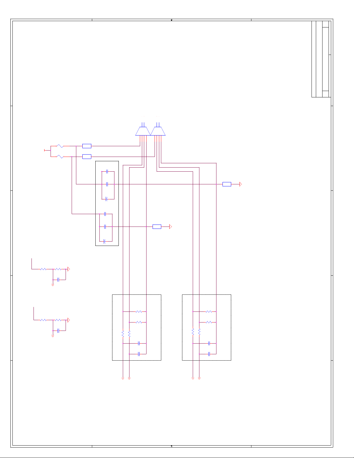
D
17 22Thursday, February 25, 1999
E
9
10
11
12
TOP of Stacked
VCC1
GND
D1-
BLM41A800S
GND
D1+
GND1
8
USB Connector
USB Stack
FB2
BLM41A800S
12
12
THIS DRAWING CONTAINS INFORMATION WHICH HAS NOT
Z1-
Z1_GND
Z1+
BOTTOM of Stacked
USB Connector
GND
GND
J2
VCC0
D0-
D0+
GND0
Z0+
1234567
FB1
12
12
Z0_GND
SMD250002
Poly fuses should be in range
of 1.5A to 5A
D
C
V5_0
F1
F2
Poly-Fuse Poly-F use
SMD250-002
USBVFIL1
USBVFIL2
8Ohm/100MHz/500mA
8Ohm/100MHz/500mA
FB3
BLM41A800S
1 2
1 2
1 2
1 2
FB4
BLM41A800S
C158
C157
C2
C23
C22
C6
0.01uF
0.1uF
100uF
Z1_VCC Z0_VCC
0.01uF
0.1uF
100uF
Z0-
E
USB Connectors
{Doc}
C
Title
Size Document Number Rev
Date: Sheet of
D
BEEN VERIFIED FOR MANUFACTURING AS AN END USER
PRODUCT. INTEL IS NOT RESPONSIBLE FOR THE
MISUSE OF THIS INFORMATION.
C
USBVFIL1
R2
10KR115K
Place these caps within 1 inch
C1
0.01UF
OC0#14OC1#14
USBVFIL2
R4
B
A
10KR315K
C7
0.01UF
of USB Connector stack
27
R95
Place As Close as
Possible to PIIX4
PCB Trace 45 Ohm Matched,
Routed Together
Stripline width 0.015 (1 oz)
44.88/45.45 Ohm
R91
15K
R90
15K
27
C122
47pF
R94
C123
47pF
USBP0+14
USBP0-14
PCB Trace 45 Ohm Matched, Routed Together
Stripline width 0.015 (1 oz) 44.88/45.45
Ohm
R89
15K
R88
15K
27
27
R93
R92
C124
47pF
Place As Close as
Possible to PIIX4
C125
47pF
USBP1-14
USBP1+14
B
NOTE 1: USB differential traces route together (Z0- & Z0+) and (Z1- & Z1+).
Must be 45 Ohm Matched
Stripline width 0.015 (for 1 oz)->44.88/45.45 Ohm.
NOTE 2: Protect differential traces w/ guard traces or
double space to any other signal.
NOTE 3: Place ferrites at connector.
NOTE 4: Poly-fuse min 1.5A
max 5A.
A
4 4
3 3
2 2
1 1
Page 83
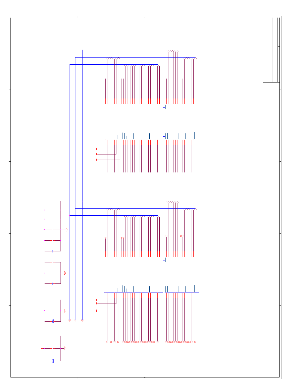
D
18 22Thursday, February 25, 1999
E
D
C
ISA Slots
V5_0
C127
C126
C42
C112
C111
0.1uF
0.1uF
0.1uF
0.1uF
0.1uF
J6
SD7RSTDRV
IOCHK#
A01
IOCHCK
GND
B01
B02 A02
SD7
IOCHK# 9,13
ISA Connectors
{Doc}
C
Title
Size Document Number Rev
Date: Sheet of
BEEN VERIFIED FOR MANUFACTURING AS AN END USER
PRODUCT. INTEL IS NOT RESPONSIBLE FOR THE
MISUSE OF THIS INFORMATION.
E
D
C
LA23
LA20
LA19
LA18
LA21
LA17
LA22
SD1
SD6
SD2
SD3
SD5
SD0
SD4
SA15
SA16
SA17
SA9
SA3
SA11
SA18
SA10
SA12
SA14
SA19
SA13
SA8
IOCHRDY
AEN
A03
A04
A05
A06
A07
A08
A09
A10
A11
A12
A13
A14
A15
A16
A17
A18
A19
A20
A21
A22
SA17
SA16
IOR
DACK3
B15
DACK3#
SA16
B16
DRQ3
SA15
SA15
SA14
DRQ3
DACK1
B17
DACK1#
SA14
SA13
SA12
DRQ1
REFRESH
B18
B19
REFRESH#
DRQ1
SA13
SA12
SA11
CLK
B20
B21
IRQ7
SYSCLK
SA11
SA10
SA10
IRQ7
SA9
IRQ6
B22
IRQ5
IRQ6
SA8
SA9
SD3
SD2
AEN
SD6
SD5
SD4
SD1
SD0
SA19
SA18
IOCHRDY
IOW
RSTDRV SD7
V5_0
B03
B04
IRQ9
SD5
SD6
SMEMR
IRQ9
-5V
DRQ2
-12V
0WS
+12V
GND
SMEMW
B05
B06
B07
B08
B09
B10
B11
B12
B13
B14
ZEROWS#
IOW#
IOR#
MEMR#
MEMW#
DRQ2
SD1
SD3
SD2
SD4
SD0
SA17
SA18
SA19
IOCHRDY 9,13,16
AEN 13,16,20
SA0
SA1
SA2
SA4
SA6
SA5
SA7
SBHE#
C01
A28
B28
BALE
SA3
SA3
BALE
C02
A29
A30
A31
SA2
SA1
SA0
LA23
SBHE
V5_0
OSC
GND
MCS16
IOCS16
B29
B30
B31
D01
D02
REF0
IOCS16#
MEMCS16#
LA23
SA2
SA0
SA1
SBHE# 9,13
A23
A24
A25
A26
A27
SA8
SA7
SA6
SA5
SA4
TC
IRQ5
IRQ4
IRQ3
DACK2
B23
B24
B25
B26
B27
IRQ4
DACK2#
TC
IRQ3
SA6
SA4
SA7
SA5
C03
D03
IRQ10
LA22
C04
LA22
IRQ10
D04
IRQ11
LA21
C05
LA21
IRQ11
D05
IRQ12
LA20
C06
LA20
IRQ12
D06
IRQ15
LA19
LA19
IRQ15
IRQ14
LA18
C07
LA18
IRQ14
D07
MEMR#
C08
C09
LA17
DACK0
D08
D09
DACK0#
DRQ0
LA17
MEMW#
C10
MEMR
MEMW
DRQ0
DACK5
D10
DACK5#
MEMW# 9,13,20
MEMR# 9,13,20
SD8
C11
D11
DRQ5
SD8
SD9
C12
SD8
DRQ5
D12
DACK6#
SD9
SD10
C13
SD9
SD10
DACK6
DRQ6
D13
DRQ6
SD10
SD12
SD11
C14
C15
SD11
DACK7
D14
D15
DACK7#
SD11
SD12 DRQ7
SD13
C16
SD12
DRQ7
D16
SD13
SD14
C17
SD13
V5_0
D17
MASTER16#
SD14
SD15
C18
SD14
SD15
MASTER
GND
D18
SD15
ISA Conn B
J5/J6 V5_0:
B03, B29, B3 1, D16
J5/J6 GND:
B01, B10, D18
J5/J6: +12V B09
-12V B07
-5V B05
THIS DRAWING CONTAINS INFORMATION WHICH HAS NOT
C8
10uF
C01
A03
A04
A05
A06
A07
A08
A09
A10
A11
A12
A13
A14
A15
A16
A17
A18
A19
A20
A21
A22
A23
SA15
SA14
DRQ3
DACK1
B17
DRQ39,14,16
DACK1#14,16
B18
SA13
SA12
DRQ1
REFRESH
B19
REFRESH#9,13
DRQ19,14,16
SA11
CLK
B20
SYSCLK13
SA9
SA10
IRQ7
IRQ6
B21
B22
IRQ69,13,14,16
IRQ79,13,14,16
A24
A25
SA8
SA7
IRQ5
IRQ4
B23
B24
B25
IRQ49,13,14,16
IRQ59,13,14,16
A26
A27
SA6
SA5
SA4
TC
IRQ3
DACK2
B26
B27
TC14,16
IRQ39,13,14,16
DACK2#14,16
C70
0.1uF
B
A
C71
0.1uF
C5
10uF
C62
0.1uF
C63
-12V +12V-5V
0.1uF
LA[23:17]
SD[15:0]
10uF
10uF
Note Cap Direc tion Note Cap Direc tion
SA[19:0]
SA[19:0]9,13,16,20
SD[15:0]9,13,16,20
LA[23:17]9,13
C4
C59
0.1uF
C60
0.1uF
C3
4 4
A01
SD3
SD2
AEN
SD6
SD5
SD4
SD1
SD0
SA19
SA17
SA16
-5V
DRQ2
B06
DRQ29,14,16
SA18
IOCHRDY
IOW
SMEMR
IOR
-12V
0WS
+12V
GND
SMEMW
DACK3
B07
B08
B09
B10
B11
B12
B13
B14
B15
B16
ZEROWS#9,13
IOR#9,13,16
DACK3#14,16
SMEMR#9,13
IOW#9,13,16,20
SMEMW#9,13
IOCHCK
GND
J5
RSTDRV SD7
V5_0
IRQ9
B01
B02 A02
B03
B04
B05
+12V +12V-12V -12V-5V -5V
IRQ99,13,14
RSTDRV13,16
3 3
C02
C03
C04
C05
C06
C07
C08
C09
C10
C11
C12
C13
C14
C15
C16
C17
MEMW
DACK5
D10
DACK5#14
C18
SD8
SD9
SD11
SD12
SD13
SD14
SD15
SD10
B
DRQ7
V5_0
MASTER
GND
DRQ5
DACK6
DRQ6
DACK7
ISA Conn A
D11
D12
D13
D14
D15
D16
D17
D18
A
MASTER16#9
DRQ59,14
DRQ79,14
DACK7#14
DRQ69,14
DACK6#14
1 1
A28
A29
A30
A31
SA3
SA2
SA1
SA0
BALE
V5_0
OSC
GND
B28
B29
B30
B31
REF08
BALE9,13
D01
LA23
SBHE
MCS16
IOCS16
D02
IOCS16#9,13
MEMCS16#9,13
LA22
LA21
IRQ10
IRQ11
D03
D04
IRQ109,13,14,16
IRQ119,13,14
LA19
LA20
IRQ12
IRQ15
D05
D06
D07
IRQ159,13,14,15,16
IRQ129,13,14,16
LA17
LA18
MEMR
IRQ14
DACK0
DRQ0
D08
D09
IRQ149,13,14,15,16
DRQ09,14,16
DACK0#14,16
2 2
Page 84
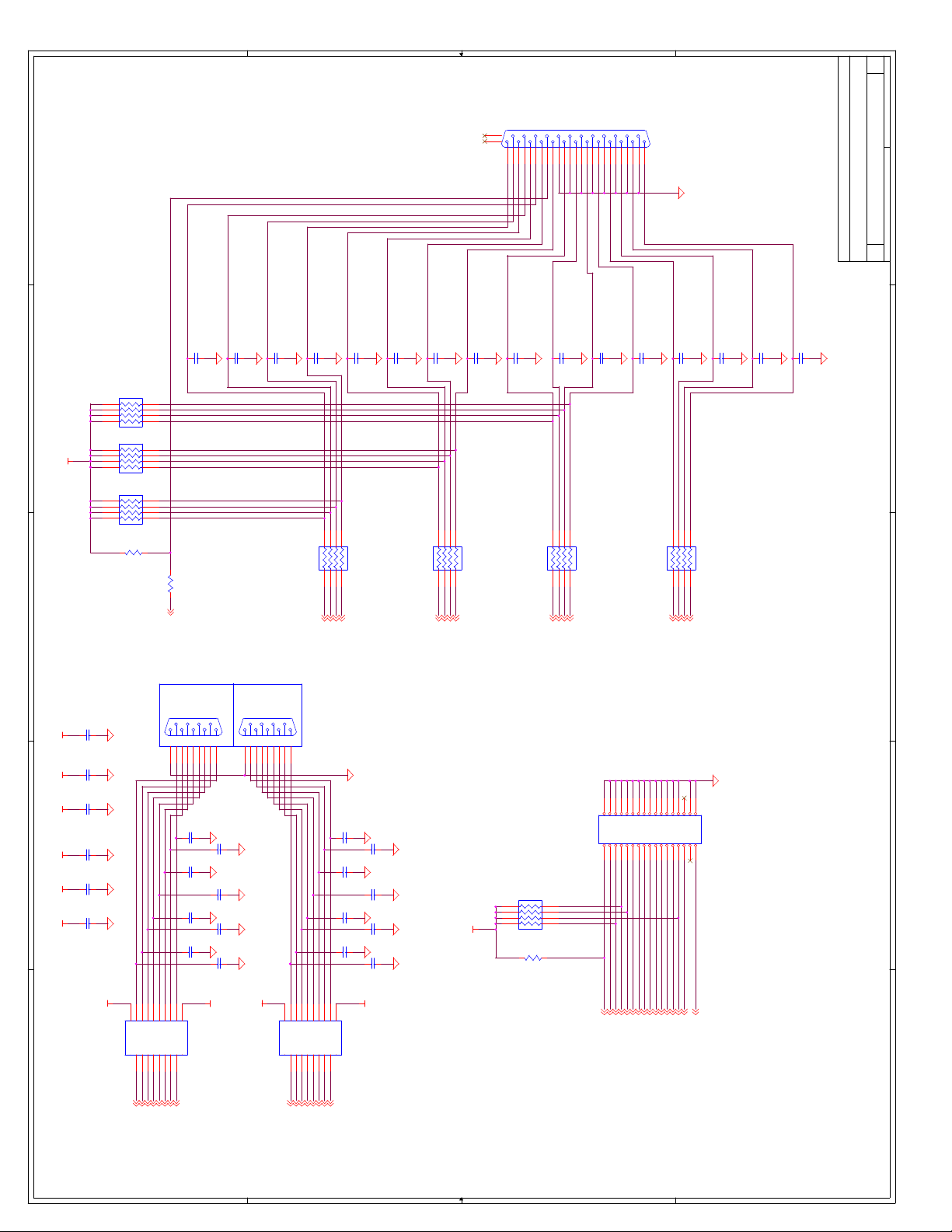
D
19 22Thursday, February 25, 1999
27
26
1
E
-PSLCTIN
-PPINIT
-PPERR
-PALF
-PSTROBE
PPDR0
PPDR1
PPDR2
PPDR3
PPDR4
PPDR5
22921820719618517416315214
PPDR6
PPDR7
J3
DB25
13251224112310
-PPBUSY
PPE
PPSLCT
-PPACK
E
COMx, DB25, Floppy
{Doc}
C
Title
Size Document Number Rev
Date: Sheet of
PARALLEL
C12
220pF
C11
220pF
C24
220pF
RP7
D
V5_0
C
4.7K
4 5
3 6
2 7
1 8
RP6
4.7K
4 5
3 6
2 7
1 8
RP5
4.7K
4 5
3 6
2 7
1 8
R7
4.7K
R9
22
-SLCTRIN16
COM0
C65
0.1uF
C48
0.1uF
J4
594837261
594837261
COM1
141813171216111510
141813171216111510
SERIAL STACK
C10
220pF
C25
C9
220pF
RP1
22
1 8
2 7
3 6
4 5
-ALF
-ERR
-INIT
-STROBE
-INIT16
-ERR16
-ALF16
-STROBE16
220pF
C13
220pF
C14
C26
220pF
RP2
33
1 8
2 7
3 6
4 5
PDR0
PDR1
PDR2
PDR3
PDR016
PDR116
PDR216
PDR316
220pF
RP3
1 8
PDR4
PDR416
2 7
PDR5
C16
220pF
C15
220pF
33
3 6
4 5
PDR6
PDR7
PDR516
PDR616
PDR716
C18
220pF
C19
C17
220pF
RP4
1 8
2 7
-ACK
-BUSY
-ACK16
-BUSY16
220pF
22
3 6
4 5
SLCT
PE
PE16
SLCT16
C21
220pF
C20
220pF
D
THIS DRAWING CONTAINS INFORMATION WHICH HAS NOT
BEEN VERIFIED FOR MANUFACTURING AS AN END USER
PRODUCT. INTEL IS NOT RESPONSIBLE FOR THE
MISUSE OF THIS INFORMATION.
C
C43
0.1uF
12345678910
1112
1314
1516
1718
1920
2122
2324
2526
2728
2930
3132
C50
470pF
C37
C64
B
A
0.1uF
V5_0 V5_0+12V +12V-12V-12V
C54
0.1uF
C49
0.1uF
+12V
COM0/COM1
SP_DSR0
SP_RXD0
SP_DCD0
12023456789
RA1
RA2
+12VV5_0
RY2
RY1
U4
19
DCD0#16
DSR0#16
4 4
SP_RTS0
RA3
DY1
DA1
RY3
RXD016
RTS0#16
SP_TXD0
DY2
DA2
TXD016
SP_RI0
SP_DTR0
SP_CTS0
RA4
DY3
DA3
RY4
CTS0#16
DTR0#16
10
RA5
-12V
RY5
GND
12131415161718
11
RI0#16
470pF
C51
470pF
C38
470pF
C52
470pF
C39
470pF
C53
470pF
C40
470pF
SP_DSR1
SP_RXD1
SP_DCD1
+12V
-12V
GD75232SOP
12023456789
RA1
RA2
+12VV5_0
RY2
RY1
U3
19
DSR1#16
DCD1#16
RA3
RY3
RXD116
SP_TXD1
SP_RTS1
DY1
DY2
DA2
DA1
RTS1#16
TXD116
SP_CTS1
SP_RI1
SP_DTR1
RA4
DY3
DA3
RY4
12131415161718
DTR1#16
CTS1#16
C44
470pF
C33
470pF
C45
470pF
C34
470pF
C46
470pF
C35
470pF
C47
470pF
C36
470pF
-12V
10
RA5
-12V
RY5
GND
GD75232SOP
11
RI1#16
3 3
V5_0
FLOPPY
RP18
1K
18
27
36
45
R25
1K
3334
JP1
B
FLOPPY HEADER 17X2
-RDATA16
-WPT16
-SIDE116
-DSKCHG16
-TRK016
2 2
-INDEX16
HDEN16
-MOTEA16
-DIR16
DRATE016
-DRVSA16
-WGATE16
-WDATA16
-STEP16
-MOTEB16
-DRVSB16
A
1 1
Page 85
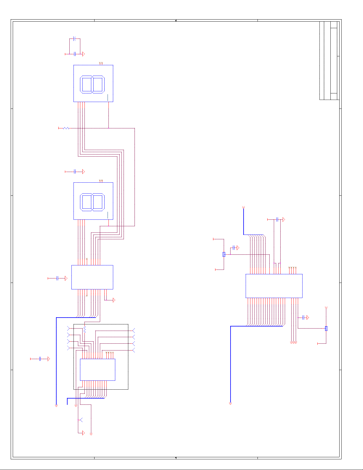
D
C145
10uF
BIOS/ Port 80
{Doc}
C
Title
Size Document Number Rev
20 22Thursday, February 25, 1999
E
Date: Sheet of
C205
0.1uF
14
R105
1
V5_0
V5_0
U13
ABC
D
3
2
13
12
10K
E
V5_0
10
4
RTDEC
LFTDEC
7
8
GND
GND
LATCH
TIL311 SOCKET
5
D
C206
0.1uF
V5_0 V5_0
14
1
V5_0
V5_0
U12
ABC
D
3
2
13
12
C
25691015161920
24
1B1
1B2
1B3
1B4
1B5
V5_0
C196
0.1uF
V5_0
C200
0.1uF
U10
1A1
1A2
1A3
1A4
1A5
347
8
SD4
SD5
SD6
SD7
TP
1
R98
TP10
TP
1
TP12
TP
1
TP14
TP
1
TP16
183
194
O2I2
O3I3
Port 80
B
V5_0
7
8
10
4
GND
GND
RTDEC
LFTDEC
XD[7:0] 13
C208
XD6
SA7
XD7
A7A8A9
8
SA8
V5_0
11
VPP
VCC
A10
A11
A12
73665432
SA9
SA10
SA11
SA12
SA13
0.1uF
THIS DRAWING CONTAINS INFORMATION WHICH HAS NOT
1231139
373038
392423
NC
NCWE#
NC
VCC
A13
SA14
NC
GND
GND
28F002BC
OE#
CE#
A14
SA15
RP#
A15
A16
A17
1
222610
40
C131
0.1uF
SA16
SA17
2
+12V
MEMW#9,13,18
MEMR#9,13,18
BIOSCS#14
LATCH
TIL311 SOCKET
5
V5_0
3
2
J21
1x3
23
2B1
2B2
2B3
2B4
2B5
2A1
2A2
2A3
1417182111
SD0
SD1
SD2
SD3
0
205
216
237
249
2510
O4I4
O5I5
O6I6
O7I7
QST3384
2A4
2A5
GND
BEA
BEB
1
22
12
13
TP
1
TP9
TP
1
TP8
TP
1
TP7
TP
1
1
81715
22
2611
2712
NC
NCO1NC
NC
O8I8
O9I9
O10I10
TP6
1
+12V
C130
0.1uF
XD0
25
U11
A0
21
20271928183217331634153514
SA0
SA1
XD1
XD2
XD3
DQ0
DQ1
DQ2A2DQ3A3DQ4A4DQ5A5DQ6A6DQ7
A1
SA2
SA3
SA4
XD4
XD5
SA5
SA6
BEEN VERIFIED FOR MANUFACTURING AS AN END USER
PWROK5 21
3
1
PRODUCT. INTEL IS NOT RESPONSIBLE FOR THE
J22
HDR3
MISUSE OF THIS INFORMATION.
D
C
B
I1/CLK
U9
2
IOW#9,13,16,18
1
SA9
TP
SD[15:0]
SA[19:0]
A
SD[15:0]9,13,16,18
4 4
I11
I12
22V10
13
16
Standard
Stuff
Option
SA4
SA1
SA0
SA5
SA3
SA2
SA6
SA7
SA8
A
TP2
Expect All 0's except
AEN13,16,18
SA7=1 for P80 Decode
3 3
SA[19:0]9,13,16,18
2 2
1 1
Page 86
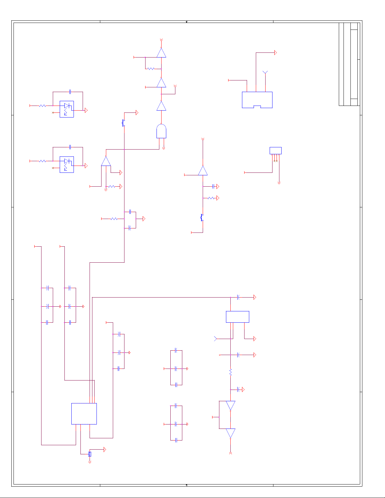
D
PWROK 4,14
21 22Thursday, February 25, 1999
U24A
R127
10K
PS_OK
U21C
U25C
U22B
74LCT14
1 2147
TP
TP1
PWROK5 20
74ACT05
5 6147
74HCT14
5 6
6
PS_OK = OR of PW_OK,-DBRESET,RESET SWITCH
74ALS00
4
5
CPUPWROK4
V3.3SUS
V3.3SUS
U24B
S1
PWRBTN# 14
3 4147
POWER SWITCH
V5_0
J12
74LCT14
C142
0.1uF
R56
10K
V5_0
1
1
2
3
1
2
3
AMP173981-3
JP2
1x41234
SPEAKER HEADER
SPKR14
E
AXT Power Connector
{Doc}
C
Title
Size Document Number Rev
Date: Sheet of
D
V3.3SUS
E
C27
470pF
R8
124
Power Indicator s
R10
D
220
V5_0 V3_3
IN
2
OUT
3
NC
1
D1
LGS260-DO
C41
470pF
Note: Add screen marking for V5_0 LED, V3_3 LED
IN
2
OUT
3
NC
1
D2
LGS260-DO
U25B
V5_0
V5_0
S2
Open Collector
74ACT05
3 4147
R128
4.7K
DBRESET4
R53
10K
RESET SWITCH
C141
0.01uF
C138
10uF
V5_0
C
-12V
B
Place at ATX Connector
A
+12V
C83
220uF
C69
220uF
C76
0.1uF
Note Cap Direction
C98
C110
C102
220uF
220uF
0.1uF
Place at ATX Connector
J11
11
8910
357
461
2
GND
GND
GND
V5_0
V5_0
V3_3
V3_3
-12V
PS_ON
GND
GND
GND
GND
V3_3
1214181920
131516
17
3
2
1
5VSB
PW_OK
-5V
V5_0
PWRON#14
-5V
C89
C88
C97
Place at ATX Connector
+12V
V5_0
ATX POW CONN
J20
JUMP3
100uF
Note Cap Direction
100uF
0.1uF
C109
100uF
C84
100uF
C96
0.1uF
C58
100uF
C72
100uF
V3_3 V5_0
C61
0.1uF
Place at ATX Connector Place at ATX Connector
TP18
V3.3SUS
TP
1
V3.3SUS
BEEN VERIFIED FOR MANUFACTURING AS AN END USER
PRODUCT. INTEL IS NOT RESPONSIBLE FOR THE
MISUSE OF THIS INFORMATION.
C
B
A
THIS DRAWING CONTAINS INFORMATION WHICH HAS NOT
C154
47uF
OutTab
2.7K
LT117-3.3
Adj/GND
1
C152
47uF
C153
10uF
74LCT14
74LCT14
U23
Out In
2 3
4
R57
98147
U24D
56147
U24C
RSMRST#14
4 4
3 3
2 2
1 1
Page 87
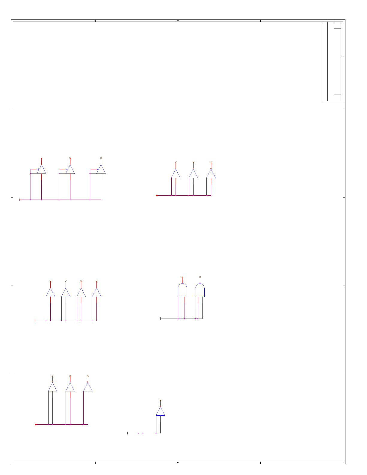
D
22 22Thursday, February 25, 1999
E
D
4
5 6
7
14
V3.3SUS
C
U15B
10
74LVC125
9 8
7
14
U15C
13
74LVC125
U15D
74LVC125
7
12 11
14
Make these connections
Cutable
U25D
74ACT05
U25E
74ACT05
U25F
9 8147
V5_0
7
11 10
14
74ACT05
7
13 12
14
Make these connections
Cutable
Unused Gates
Title
THIS DRAWING CONTAINS INFORMATION WHICH HAS NOT
BEEN VERIFIED FOR MANUFACTURING AS AN END USER
{Doc}
C
Size Document Number Rev
PRODUCT. INTEL IS NOT RESPONSIBLE FOR THE
MISUSE OF THIS INFORMATION.
E
Date: Sheet of
D
C
U2C
74AS07
U2D
74AS07
U2E
74AS07
U2F
5 6147
9 8147
11 10
14
B
U21D
74HCT14
U21E
74HCT14
9 8147
A
V5_0 V5_0
4 4
U21F
7
11 10
14
14
74AS07
7
7
13 12
14
Make these connections
74HCT14
7
13 12
Make these connections
Cutable
Cutable
V3.3SUS
V5_0
U24F
13 12
14
3 3
U22C
9
7
10814
74LCT14
7
Make these connections
Cutable
74ALS00
U22D
74ALS00
7
12
131114
B
Make these connections
Cutable
A
2 2
1 1
Page 88
111Tuesday, May 11, 1999
1
Embedded Microcontroller Division (EMD)
Intel Corporation
5000 W. Chandler Blvd
Chandler AZ, 85044
2
Celeron Processor Adaptor A
Title Page / Revision
C
Title
Size Document Number Rev
1
Date: Sheet of
2
3
4
Revision
Celeron(TM) Processor
5
in PPGA Daughter Board
A1
Intel disclaims all liability, including liability for
No license, express or implied, by estoppel or otherwise, to any
infringement of any proprietary rights, relating to use of
intellectual property rights is granted herein.
THIS SCHEMATIC IS PROVIDED "AS IS" WITH NO WARRANTIES
WHATSOEVER, INCLUDING ANY WARRANTY OF MERCHANTABILITY,
FITNESS FOR ANY PARTICULAR PURPOSE, OR ANY WARRANTY
OTHERWISE ARISING OUT OF PROPOSAL, SPECIFICATION OR
SAMPLE.
information in this specification. Intel does not warrant or
represent that such use will not infringe such rights.
THIS DRAWING CONTAINS INFORMATION WHICH HAS NOT
3
BEEN VERIFIED FOR MANUFACTURING AS AN END USER
PRODUCT. INTEL IS NOT RESPONSIBLE FOR THE
MISUSE OF THIS INFORMATION.
4
5
History
REV A0 to REV A1 Changes
1. Removed Translator logic for
PREQ0#
2. Removed Termination Resistors on
BX side for GTL+
3. Added 20pF load on HCLK for BX
clock compensating
D D
C C
B B
A A
Page 89
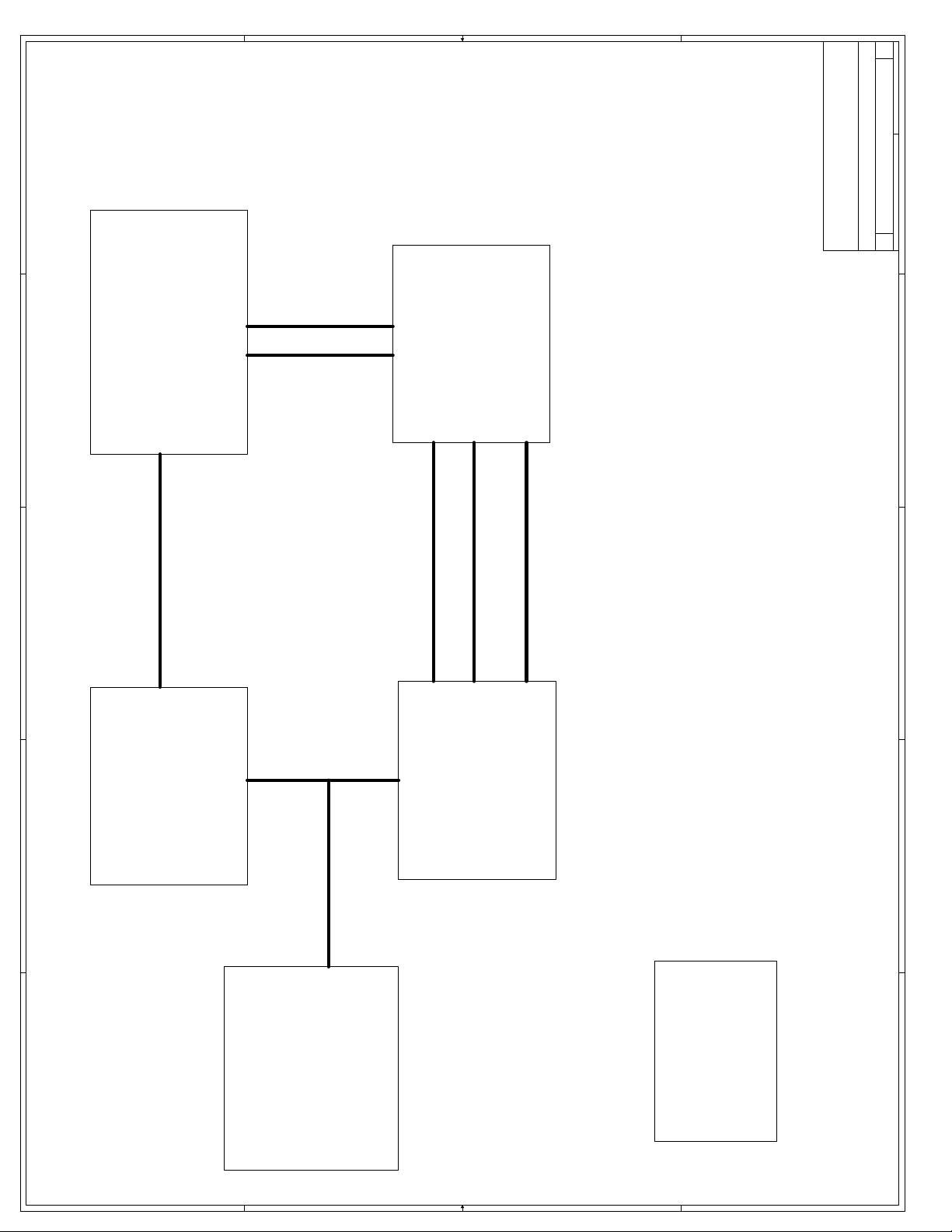
211Tuesday, May 11, 1999
1
Embedded Microcontroller Division (EMD)
Intel Corporation
5000 W. Chandler Blvd
Chandler AZ, 85044
Title
Diagram
1
Celeron Processor Adaptor A
C
Size Document Number Rev
Date: Sheet of
SMBus
2
CPU
Connector
Page 9
ITP
Bus Ratio
Logic
Thermal Sensor
Page 10
THIS SCHEMATIC IS PROVIDED "AS IS" WITH NO
WARRANTIES WHATSOEVER, INCLUDING ANY
PCI Bus
AGP Bus
SDRAM
Interface
3
2
WARRANTY OF MERCHANTABILITY, FITNESS FOR
ANY PARTICULAR PURPOSE, OR ANY WARRANTY
OTHERWISE ARISING OUT OF PROPOSAL,
SPECIFICATION OR SAMPLE.
3
440BX
4
Socket 370
Page 3&4
Page 7&8
4
GTL+
5
Voltage
Regulator
Page 11
GTL+
Termination
Page 5 & 6
D D
C C
B B
A A
5
Page 90

R8
270
VCC_CMOS
R7
270
E
311Tuesday, May 11, 1999
E
HD#[63:0] 5,6,7
HD#12
HD#6
HD#5
HD#2
HD#7
HD#3
HD#4
HD#0
HD#1
HD#8
W1T4N1M6U1S3T6J1S1P6Q3M4Q1L1N3U3H4R4P4H6L3G1F8G3K6E3E1
D#0
D#1
D#2
D#3
D#4
D#5
D#6
D#7
D
U1A
A#3
A#4
A#5
A#6
A#7
A#8
A#9
A#10
AL9
AK8
AH8
AN9
AH6
AL15
AH12
AH10
HA#6
HA#9
HA#5
HA#10
HA#4
HA#11
HA#7
HA#3
HA#8
C
HA#[31:3]5,6,7
HD#16
HD#13
HD#10
HD#15
HD#14
HD#9
D#8
D#9
D#10
D#11
D#12
D#13
D#14
D#15
D#16
Host Interface
370 Pin Socket
A#11
A#12
A#13
A#14
A#15
A#16
A#17
A#18
A#19
Z6
AL7
AL5
AE1
AN5
AN7
AG3
AK10
AK14
HA#16
HA#14 HD#11
HA#19
HA#17
HA#12
HA#18
HA#15
HA#13
HD#17
D#17
A#20
AC3
HA#20
HD#18
D#18
A#21
AJ1
HA#21
HD#19
AE3
HA#22
D#19
A#22
HD#20
D#20
A#23
AB6
HA#23
HD#21
AB4
HA#24
V2_5
D#21
A#24
HD#22
D#22
A#25
AF6
HA#25
HD#23
D#23
A#26
Y3
HA#26
HD#25
HD#30
HD#28
HD#26
HD#29
HD#31
HD#24
HD#27
HD#32
F12A5A3J3C5F6C1C7B2C9A9D8D10
D#24
D#25
D#26
D#27
D#28
D#29
D#30
D#31
A#27
A#28
A#29
A#30
A#31
AA1
AK6Z4AA3
AD4
HA#31
HA#27
HA#29
HA#30
HA#28
R1
270
AN29
D#32
BRO#
BREQ0#5,6,7
HD#33
D#33
ADS#
AN31
ADS#5,6,7
R2
HD#34
D#34
BNR#
AH14
BNR#5,6,7
1K
HD#35
AN17
D#35
BPRI#
BPRI#5,6,7
HD#36
D#36
LOCK#
AK20
HLOCK#5,6,7
HD#38
HD#37
D#37
DEFER#
AN19
DEFER#5,6,7
D#38
TRDY#
AN25
HTRDY#5,6,7
HD#39
D#39
DBSY#
AL27
DBSY#5,6,7
HD#40
C15
D#40
DRDY#
AN27
DRDY#5,6,7
HD#41
D14
D#41
HD#42
D12A7A11
D#42
HIT#
AL25
HIT#5,6,7
HD#43
AL23
HD#44
D#43
HITM#
HITM#5,6,7
D#44
HD#45
C11
D#45
A20M#
AE33
HD#46
A21
AE37
HD#47
A15
D#46
D#47
FLUSH#
IGNNE#
AG37
HD#48
A17
D#48
INIT#
AG33
HD#50
HD#49
HD#51
C13
C25
A13
D#49
D#50
LINT0/INTR
LINT1/NMI
J37
L37
M36
HD#52
HD#53
D16
A23
D#51
D#52
PREQ#
PWRGOOD
AJ35
AK26
D#53
SMI#
HD#54
C21
D#54
SLP#
AH30
HD#55
C19
D#55
STPCLK#
AG35
HD#56
C27
D#56
HD#57
A19
AJ33
HD#58
HD#59
HD#60
C23
C17
A25
D#57
D#58
D#59
BSEL#
FERR#
IERR#
AE35
AC35
IERR#
FERR#_CPU
1
TP
TP1
VCCCORE
HD#63
HD#62
HD#61
A27
E25
D#60
D#61
D#62
THERMTRIP#
THERMDP
AL31
AH28
THERMDP10
R4515%
F16
D#63
THERMDN
AL29
THERMDN10
CPURES#
C37
AG1
HREQ#1
HREQ#0
AK18
AH16
REQ#0
REQ#1
EDGCTRL
RTTCTRL
SLEWCTRL
S35
E27
HREQ#2
HREQ#3
AH18
AL19
REQ#2
E21
VCOREDET
1
R6
R5
110 1%
HREQ#[4:0] 5,6,7
HREQ#4
AL17
REQ#3
REQ#4
VCOREDET
TP
TP2
110 1%
1%
1%
RS#0
AH26
RS#0
BPM0#
C35
RS#1
AH22
E35
RS#2
AK28
RS#1
BPM1#
G33
RS#2
BP2#
RS#[2:0] 5,6,7
HCLK0 9
PICCLK 9
Embedded Microcontroller Division (EMD)
20 pF necessary to correct
for 443BX Clock loading.
C1
20pF
R9
0
W37
J33
J35
L35
BCLK
PICD1
PICD0
PICCLK
BP3#
TCK
TDI
E3 7
AL33
AK32
AN35
TDI10
TCK10
SCK370_10
TMS
TRST#
TDO
PRDY#
RESET#
X4
A35
AN33
AN37
0.1uF
v12_0
TRST#10
TDO10
PRDY#5,10
TMS10
HRESET#5,7
CPU Fan Connector
C2
0
R78
Do Not Populate
123
J1
CON3
Celeron Processor Adaptor A
Socket370_A
C
Intel Corporation
5000 W. Chandler Blvd
Chandler AZ, 85044
Title
Size Document Number Rev
Date: Sheet of
D
THIS SCHEMATIC IS PROVIDED "AS IS" WITH NO
WARRANTIES WHATSOEVER, INCLUDING ANY
WARRANTY OF MERCHANTABILITY, FITNESS FOR
ANY PARTICULAR PURPOSE, OR ANY WARRANTY
OTHERWISE ARISING OUT OF PROPOSAL,
SPECIFICATION OR SAMPLE.
C
R3
1K
VCC_CMOS
B
V3_3
A
Voltage Translators
4 4
4 5
3
6
2
7
1
8
RP2
1K
4 5
3
6
2
7
1
8
RP1
1K
246810
1Y2Y3Y4Y5Y
VCCGND
147
U2
1A4A2A3A5A
193
5
11
Needed for CuMine
INIT#9
INTR_CPU10
A20M#_CPU10
IGNNE#_CPU10
3 3
Needed for Processors
Manufactured on .18u Process
B
A
BSEL#9
FERR#_CPU
VCC_CMOS
3.3K
R13
5%
Do Not
Populate
Do Not
Populate
R10
VCC_CMOS
FERR# 9
0
R12
330
2
3
1
Q1
5%
R11
3.3K
MMBT3904
FERR# Voltage Translator
1 1
12
6Y
6A
13
74LVC07A
NMI_CPU10
246810
1Y2Y3Y4Y5Y
147
V3_3
U3
1A4A2A3A5A
193
PWROK_GEN7,9
PREQ#10
VCCGND
5
SMI#9
SLP#9
STPCLK#9
12
6Y
6A
11
13
74LVC07A
2 2
V2_5
Page 91

411Tuesday, May 11, 1999
10V
10V
X5R
C19
VCCCORE VCCCORE
1uF
10V
X5R
C18
1uF
10V
X5R
C17
1uF
10V
X5R
C16
1uF
10V
X5R
C15
1uF
VCCCORE
10V
X5R
C14
1uF
10V
X5R
C13
1uF
10V
X5R
C12
1uF
10V
X5R
C11
1uF
10V
X5R
C10
1uF
VCCCORE
E
C9
D
VGTLREF_CPU
C
0.1uF
C8
0.1uF
C7
0.1uF
C6
0.1uF
C5
0.1uF
C4
0.1uF
C3
0.1uF
**REFERENCE VOLTAGE FOR PROCESSOR. THERE
ARE 8 VREF PINS. PLACE ONE CAPACITOR
NEAR EVERY 2 VREF PINS.
10V
X5R
C29
4.7uF
10V
X5R
C28
4.7uF
10V
X5R
C27
4.7uF
10V
X5R
C26
4.7uF
10V
X5R
C25
4.7uF
VCCCORE
10V
X5R
C24
1uF
10V
X5R
C23
1uF
10V
X5R
C22
1uF
10V
X5R
C21
1uF
10V
X5R
C20
1uF
VCCCORE
X5R
C39
4.7uF
10V
Layout: Route trace
through resistor
C47
4.7uF
C46
4.7uF
C45
4.7uF
C44
1uF
C43
1uF
C42
1uF
C41
1uF
C40
1uF
VCCCORE
1
R14
L1
X5R
10V
X5R
10V
X5R
10V
X5R
10V
X5R
10V
X5R
10V
X5R
10V
X5R
22 uH
Spare Decoupling Caps: Do Not Populate
Low Q, Self-resonance >10MHz
Series resitance 1 Ohm Typ,
1.5Ohm Max
Rated current >=30 mA
LQG21C220N00T1
Embedded Microcontroller Division (EMD)
Intel Corporation
5000 W. Chandler Blvd
Chandler AZ, 85044
THIS DRAWING CONTAINS INFORMATION WHICH HAS NOT
10V
X5R
C38
4.7uF
10V
X5R
C37
4.7uF
10V
X5R
C36
4.7uF
VCCCOREVCCCORE
10V
X5R
C35
4.7uF
10V
X5R
C34
1uF
10V
X5R
C33
1uF
10V
X5R
C32
1uF
10V
X5R
C31
1uF
10V
X5R
C30
1uF
VID[3:0] 11
E
Celeron Processor Adaptor A
Socket370_B
C
Title
Size Document Number Rev
Date: Sheet of
D
BEEN VERIFIED FOR MANUFACTURING AS AN END USER
PRODUCT. INTEL IS NOT RESPONSIBLE FOR THE
MISUSE OF THIS INFORMATION.
C
C49
22uF
16V
Place within 2" of Pin
VCC_1.5
AD36
Route as a Pair
W33
PLL1
VCC_CMOS
VCC_2.5
Z36
AB36
Tantalum
Tantalum +-30%
Series resistance 1 Ohm Max
Series inductance 2 nH Typ
U33
PLL2
B
SCK370_10
C48
C139
0.1uF
4.7uF
10V
X5R
A
VID2
VID0
VID1
Z34
GND
VREF0
E33
AJ31
F18
Y33
GND
VREF1
K4R6V6
GND
VREF2
VREF3
AL35
VREF4
AD6
AM36
VID0
VREF5
AK12
AL37
VID1
VREF6
AK22
VID3
AJ37
VID2
VREF7
VCC_CMOS V2_5 VTT
VID3
Make MREF as short and fat as possible.
Use at least 24 mill line.
A37
AB32
AC33
AC5
AD2
AD34
AF32
AF36
AG5
AH2
AH34
AJ11
AJ15
AJ19
AJ23
AJ27
AJ3
AJ7
AK36
AK4
AL1
AL3
AM10
AM14
AM18
AM2
AM22
AM26
AM30
AM34
AM6
AN3
B12
B16
B20
B24
B28
B32B4B8
D18D2D22
D26
D30
D34D4E11
E15
E19E7F20
F24
F28
F32
F36G5H2
H34
K36L5M2
M34
P32
P36Q5R34
T32
T36U5V2
V34
X32
X36
Y37Y5Z2
GND
GND
GND
GND
GND
GND
GND
GND
GND
GND
GND
GND
GND
GND
GND
GND
GND
GND
GND
GND
GND
GND
GND
GND
GND
GND
GND
GND
GND
GND
GND
GND
GND
GND
GND
GND
GND
GND
GND
GND
GND
GND
GND
GND
GND
GND
GND
GND
GND
GND
GND
GND
GND
GND
GND
GND
GND
GND
GND
GND
GND
GND
GND
GND
GND
GND
GND
GND
GND
GND
GND
GND
GND
GND
GND
GND
GND
B
Power Supply
370 Pin Socket
U1B
VCC_CORE
VCC_CORE
VCC_CORE
VCC_CORE
VCC_CORE
VCC_CORE
VCC_CORE
VCC_CORE
VCC_CORE
VCC_CORE
VCC_CORE
VCC_CORE
VCC_CORE
VCC_CORE
VCC_CORE
VCC_CORE
VCC_CORE
VCC_CORE
VCC_CORE
VCC_CORE
VCC_CORE
VCC_CORE
VCC_CORE
VCC_CORE
VCC_CORE
VCC_CORE
VCC_CORE
VCC_CORE
VCC_CORE
VCC_CORE
VCC_CORE
VCC_CORE
VCC_CORE
VCC_CORE
VCC_CORE
VCC_CORE
VCC_CORE
VCC_CORE
VCC_CORE
VCC_CORE
VCC_CORE
VCC_CORE
VCC_CORE
VCC_CORE
VCC_CORE
VCC_CORE
VCC_CORE
VCC_CORE
VCC_CORE
VCC_CORE
VCC_CORE
VCC_CORE
VCC_CORE
VCC_CORE
VCC_CORE
VCC_CORE
VCC_CORE
VCC_CORE
VCC_CORE
VCC_CORE
VCC_CORE
VCC_CORE
VCC_CORE
VCC_CORE
VCC_CORE
VCC_CORE
VCC_CORE
VCC_CORE
VCC_CORE
VCC_CORE
VCC_CORE
VCC_CORE
VCC_CORE
VCC_CORE
B6
AJ5
AH32
AH36
AJ9
AK2
AJ13
AJ17
AJ21
AJ25
AJ29
AK34
AM12
AM16
AM20
AM24
AM28
AM32
AM4
AM8
AF2
AA5
AB2
AE5
AF34
AA37
AB34
AD32
AH24
VCCCORE
A
C3
B10
B14
B18
B22
B26
B30
B34
E5
D6
E13
E17
D20
D24
D28
D32
D36
E9
F14F2F22
F4
K2
P2
S5
F26
F30
F34
N5
K32
K34
H32
H36
P34
R32
R36
M32
J5
VCC_CORE
T2
T34
Z32
Y35
V32
V36W5X34
VGTLREF_CPU
C140
0.1uF
C141
0.1uF
C142
0.1uF
4 4
3 3
2 2
1 1
Page 92

511Tuesday, May 11, 1999
1
Embedded Microcontroller Division (EMD)
Intel Corporation
5000 W. Chandler Blvd
Chandler AZ, 85044
2
GTL Termination
Title
Size Document Number Rev
1
Celeron Processor Adaptor A
C
Date: Sheet of
2
3
4
Resistor Packs placed for Dual End Termination.
Not used on Celeron Processor in PPGA package with
Single End Termination.
THIS DRAWING CONTAINS INFORMATION WHICH HAS NOT
3
BEEN VERIFIED FOR MANUFACTURING AS AN END USER
PRODUCT. INTEL IS NOT RESPONSIBLE FOR THE
MISUSE OF THIS INFORMATION.
4
5
GTL+ TERMINATION
RESISTORS-BX
D D
C C
B B
A A
5
Page 93

611Tuesday, May 11, 1999
1
C79
0.1uF
16V
4 5
HA#25
4 5
4 5
X7R
C81
0.1uF
16V
X7R
Embedded Microcontroller Division (EMD)
Intel Corporation
5000 W. Chandler Blvd
C78
0.1uF
16V
X7R
C80
0.1uF
16V
X7R
Place one Cap near every two R-packs
VTT
678
RP57
56 ohm
56 ohm
56 ohm
56 ohm
123
4 5
HD#10
HD#18
HD#2
HD#12
VTT
678
RP51
56 ohm
123
4 5
HA#7
HREQ#1
BNR#
HREQ#4
VTT
678
RP45
56 ohm
123
4 5
NOTE : VTT = TERMINATION
VOLTAGE
Chandler AZ, 85044
THIS DRAWING CONTAINS INFORMATION WHICH HAS NOT
C69
0.1uF
16V
C67
0.1uF
16V
X7R
VTT
C66
0.1uF
16V
X7R
VTT
678
RP58
123
2
3
HD#51
HD#47
HD#41
HD#49
VTT
678
RP52
123
HREQ#2
HREQ#0
BPRI#
DEFER#
VTT
678
RP46
123
HD#1
HD#15
HD#4
HD#6
VTT
678
RP40
123
X7R
C68
0.1uF
16V
X7R
VTT
678
RP59
56 ohm
123
4 5
HD#55
HD#57
HD#63
VTT
678
RP53
56 ohm
4 5
123
HD#62
HD#60
HD#61
VTT
678
RP47
56 ohm
123
4 5
HA#5
HA#12
HA#13
VTT
678
RP41
56 ohm
123
4 5
C71
C70
4 5
HD#46
4 5
HD#56
4 5
HA#15
4 5
56 ohm
56 ohm
56 ohm
56 ohm
0.1uF
0.1uF
VTT
VTT
VTT
VTT
C73
16V
X7R
16V
X7R
C72
RP60
123
HD#40
RP54
123
ADS#
RP48
123
RP42
123
678
HD#52
HD#48
678
RS#2
BREQ0#
678
678
4 5
HD#59
4 5
DBSY#
4 5
HA#28
4 5
0.1uF
0.1uF
56 ohm
56 ohm
56 ohm
56 ohm
C75
0.1uF
16V
16V
16V
X7R
X7R
X7R
VTT
VTT
VTT
VTT
C77
0.1uF
16V
X7R
C74
0.1uF
16V
X7R
C76
0.1uF
16V
X7R
678
RP61
56 ohm
123
4 5
RS#1
HITM#
HREQ#3
HLOCK#
VTT
56 ohm
56 ohm
56 ohm
678
RP56
123
HA#21
HA#10
HA#19
VTT
678
RP50
123
HD#32
HD#31
VTT
678
RP44
123
RP55
RP49
RP43
123
HA#24
123
HD#28
123
HA#23
HD#38
678
HA#27
678
HD#34
678
4 5
HA#30
4 5
HD#43
4 5
1
Celeron Processor Adaptor A
GTL Termination
C
Title
Size Document Number Rev
Date: Sheet of
2
3
BEEN VERIFIED FOR MANUFACTURING AS AN END USER
PRODUCT. INTEL IS NOT RESPONSIBLE FOR THE
MISUSE OF THIS INFORMATION.
VTT
678
RP33
4
5
123
RS#0
HIT#
DRDY#
GTL+ TERMINATION
RESISTORS-CPU
4 5
HTRDY#
56 ohm
HD#30
678
HA#8
HA#3
HD#24
4 5
HA#11
HA#4
HD#32HD#0
HA#5
HD#33
HD#1
56 ohm
HA#6
HA#7
HD#35
HD#34
HD#2
HD#3
VTT
HA#8
HD#36
HD#4
HA#9
HD#37
HD#5
RP35
HA#10
HD#38
HD#6
HD#5
123
HA#6
HA#11
HD#39
HD#7
HD#8
HA#9
HA#12
HD#40
HD#8
HD#17
678
HA#3
HA#13
HD#41
HD#9
HD#7
HD#11
VTT
RP34
123
HA#4
HA#14
HD#9
4 5
HA#16
HA#14
HD#42
HD#10
HA#15
HD#43
HD#11
56 ohm
HA#16
HD#44
HD#12
HA#17
HD#45
HD#13
VTT
HA#18
HD#46
HD#14
HA#19
HD#47
HD#15
RP36
HA#20
HD#48
HD#16
HD#22
123
HA#22
HA#21
HD#49
HD#17
HD#36
HA#17
HA#22
HD#50
HD#18
678
HA#31
HA#23
HD#51
HD#19
4 5
HA#20
HA#24
HD#52
HD#20
HA#25
HD#53
HD#21
56 ohm
HA#26
HD#54
HD#22
HA#27
HD#55
HD#23
HA#28
HD#56
HD#24
VTT
HA#29
HD#57
HD#25
HA#30
HD#58
HD#26
RP37
HA#31
HD#59
HD#27
HD#45
123
HA#29
HD#60
HD#28
HD#44
HA#26
HD#61
HD#29
HD#42
678
HA#18
HD#62
HD#30
HD#27
4 5
HD#0
HD#63
HD#31
56 ohm
VTT
RP38
HREQ#1
HREQ#0
HA#[31:3]
3,6,7
HD#[63:0]3,6,7
HD#53 HD#29
HD#54
123
HD#21
HD#23
HREQ#2
HREQ#3
BPRI#
HD#58
678
HD#16
HREQ#4
DBSY#
DBSY#3,6,7
BPRI#3,6,7
HD#50
4 5
HD#26
HREQ#[4:0]3,6,7
DRDY#
DEFER#
DEFER#3,6,7
56 ohm
RS#0
DRDY#3,6,7
VTT
RS#2
RS#1
BREQ0#
BNR#
BREQ0#3,6,7
HD#33
HD#35
HD#25
HD#19
678
RP39
56 ohm
123
4 5
HD#20
HD#13
HD#14
HD#3
RS#[2:0]3,6,7
VTT
R77
51
HTRDY#
HITM#
HLOCK#
ADS#
HIT#
HIT#3,6,7
HTRDY#3,6,7
BNR#3,6,7
HITM#3,6,7
ADS#3,6,7
HLOCK#3,6,7
PRDY#3,10
4
5
HD#39
HD#37
D D
C C
B B
A A
Page 94

VAGPREF
711Tuesday, May 11, 1999
GAD25
GAD24
AD24
AD25
GAD26
GAD25
AD25
D5
AD26
GAD27
GAD26
GAD27
AD26
AD27
B4U2B5L5A5L3E6
AD27
GAD28
GAD28
AD28
AD28
GAD29
GAD29
AD29
AD29
GAD30
GAD30
AD30
AD30
GAD31
R2
GAD31
AD31
AD31
GC/BE#[3:0] 9
GC/BE#0
AB2
GC/BE0#
C/BE0#
C/BE#0
GC/BE#1
GC/BE#2
GC/BE1#
C/BE1#
E4
G3
C/BE#1
C/BE#2
GC/BE#3
GC/BE2#
GC/BE3#
C/BE2#
C/BE3#
C4
C/BE#3
G_FRAME# 9
G_DEVSEL# 9
W3
GFRAME#
GDEVSEL#
FRAME#
DEVSEL#
F3
E2
FRAME#9
DEVSEL#9
G_IRDY# 9
GIRDY#
INTERFACE
AGP
IRDY#
E1
IRDY#9
G_TRDY# 9
W4
Y1
GTRDY#
TRDY#
F5
F4
TRDY#9
G_STOP# 9
G_PAR 9
Y2
GPAR
GSTOP#
STOP#
PAR
G5
STOP#9
PAR9
SERR#
F2
SERR#9
G_REQ# 9
G_GNT# 9
GGNT#
GREQ#
PLOCK#
PLOCK#9
G_CLKOUT 9
G_CLKIN 9
SB-STB 9
G_CLKOUT
SBA0
N3
K1
P5
N5
SB-STB
GCLKIN
GCLKOUT
PCI ARB & PWR
MGT
PREQ0#/IOREQ#
PHOLD#
PHLDA#
WSC#
A6
AE3
PHLDA#9
PHOLD#9
PREQ0#9
SBA[7:0] 9
SBA1
SBA2
M2
M1
SBA0
SBA1
PREQ1#
PREQ2#
D8
F10
PREQ1#9
PREQ2#9
SBA3
N2
SBA2
SBA3
PREQ3#
PREQ4#
D10
PREQ3#9
PREQ4#9
SBA4
SBA5
SBA7
SBA6
P4
P3B3R1
SBA4
SBA5
SBA6
SBA7
PGNT0#/IOGNT#
PGNT1#
PGNT2#
E7
E8
D7
E10
PGNT0#9
PGNT1#9
PGNT2#9
RBF# 9
M4
RBF#
PGNT3#
PGNT4#
E9
PGNT3#9
PGNT4#9
ST[2:0] 9
PIPE# 9
M3
PIPE#
BX-PWROK
AF3
PWROK_GEN3,9
ST1
ST0
L4
L2
ST0
ST1
CLKRUN#
AC4
CLKRUN#9
ST2
L1
B2
ST2
PCLKIN
PCLK9
GADSTB-A 9
GADSTB-B 9
GADSTB-B
GADSTB-A
SUSTAT#
C2
AD4
N4J4T5C7AC2
AGPREFV
REFVCC
C88
0.1uF
R18
10K
G_CLKIN
C83
0.1uF
443BX_10
C86
R16
10K
0.1uF
Do Not StuffDo Not Stuff
Embedded Microcontroller Division (EMD)
Intel Corporation
5000 W. Chandler Blvd
Chandler AZ, 85044
Do Not Stuff
1
Celeron Processor Adaptor A
440BX
C
Title
Size Document Number Rev
Date: Sheet of
2
1
2
GAD[31:0] 9
GAD12
GAD15
GAD2
GAD0
AB5
AE2
AD3C6AD2
GAD0
GAD1
AD0
AD1
U4-2
K6
K2
K4
AD2
AD0
AD1
GAD2
AD2
GAD3
K3
AD3
GAD3
AD3
AD1
K5
AD4
GAD4
AD4
GAD5
AC3
J1W5J2
AD5
GAD5
AD5
GAD10
GAD11
GAD7
GAD8
AC1
AB4
AB1
AA5
AA3
AA4
AA2
AA1
GAD6
GAD7
GAD8
GAD9
GAD10
GAD11
GAD12
GAD13
AD6
AD7
AD8
AD9
AD10
AD11
AD12
AD13
J5
H2
H1
H3F1H5B6H4
G1V5G2D6G4
AD9
AD8
AD12
AD7
AD13
AD6
AD10
AD11
GAD13
GAD6
GAD4
GAD9
GAD1
GAD22
GAD20
GAD17
GAD19
GAD18
GAD21
GAD14
GAD16
Y5
Y3
GAD14
GAD15
492 BGA
82443BX
AD14
AD15
AD14
AD15
AD16
GAD24
GAD23
W1V2W2U5V1U4U3U1T3T4T2T1U6R3R4
GAD16
GAD17
GAD18
GAD19
GAD20
GAD21
GAD22
GAD23
PCI
INTERFACE
AD16
AD17
AD18
AD19
AD20
AD21
AD22
AD23
A2
E5V4A4
D1P2D3
D2Y4C1
C3
D4
AD19
AD23
AD17
AD18
AD20
AD24
AD21
AD22
THIS DRAWING CONTAINS INFORMATION WHICH HAS NOT
BEEN VERIFIED FOR MANUFACTURING AS AN END USER
PRODUCT. INTEL IS NOT RESPONSIBLE FOR THE
10V
X5R
C98
0.01uF
10V
X5R
C97
0.01uF
0.01uF
10V
X5R
C96
0.01uF
10V
X5R
C95
0.01uF
10V
X5R
C94
16V
X5R
C93
0.1uF
16V
X5R
C92
0.1uF
16V
X5R
C91
0.1uF
16V
X5R
C90
0.1uF
0.1uF
16V
X5R
C89
MISUSE OF THIS INFORMATION.
3
4
5
HD#55
A9
HD54#
N23
HCLK1
R79
HD#56
HD55#
HCLKIN
M25
HCLK19
HD#57
HD#58
D9
HD56#
HD57#
TESTIN#
M26
0
HD#59
HD#60
C11
HD58#
HD59#
CRESET#
PCIRST#
A3
CRESET#10
PCIRST#9
C10
HD#61
B8A7E11
HD60#
V3_3
HD#62
A8
HD61#
M23
VTT VGTLREF_B X
V5_0
V3_3
HD#63
B9
HD62#
HD63#
GTLREFA
GTLREFB
E16
1K
R80
R15
D1
31
2
VTTA
VTTB
F17
P22
M24
1K
BAT54
RESVA
RESVB
AE22
SUS_STAT1#9
RESVC
AE23
Note: PCI 5V
C82
0.1uF
RESVD
AB22
C87
0.1uF
R17
10K
HCLK1
443BX_10
VGTLREF_BX
C85
0.01uF
C84
Place as close as
Are these suppose to be 0.001uF?
0.01uF
possible to BX
V3_3 V3_3
3
4
5
AD[31:0]9
HD#[63:0] 3,5,6
HD#0
HD#1
HD#2
HD#3
HD#4
HD#5
HD#6
HD#7
HD#8
HD#9
HD#10
HD#11
HD#12
HD#13
HD#14
HD#15
HD#16
HD#17
HD#18
HD#19
HD#20
HD#21
HD#22
HD#23
HD#24
D19
HD6#
HA9#
C20
HD7#
HA10#
G22
HA#10
B21
F22
HA#11
HD8#
HA11#
HA#12
E20
F23
A20
HD9#
HA12#
F24
HA#13
E19
HD10#
HA13#
F25
HA#14
B20
HD11#
HA14#
E23
HA#15
E18
HD12#
HA15#
E26
HA#16
D20
D18
C19
HD15#
HD14#
HD16#
HD13#
82443BX
HA16#
HA17#
HA18#
HA19#
E25
B25
D25
D26
HA#17
HA#18
HA#19
HA#20
A18
B19
A19
B18
C17
HD19#
HD18#
HD17#
HD20#
HD21#
HD22#
492 BGA
HOST INTERFACE
HA20#
HA21#
HA22#
HA23#
HA24#
HA25#
A25
A24
C26
C25
D24
HA#21
HA#22
HA#23
HA#24
HA#25
E17
HD23#
HA26#
C23
HA#26
D17
B24
HA#27
E21
A22
D21
C21
A21
B22
D22
HD2#
HD3#
HD4#
HD5#
HD0#
HD1#
HA3#
HA4#
HA5#
HA6#
HA7#
HA8#
U4-1
F26
H22
H23
G25
G23
G24
G26
HA#3
HA#4
HA#5
HA#6
HA#7
HA#8
HA#9
HA#[31:3]3,5,6
HD#25
B17
HD24#
HA27#
C24
HA#28
HD#26
C16
HD25#
HA28#
A23
HA#29
HD#27
A17
HD26#
HA29#
E22
HA#30
HD#28
C15
HD27#
HA30#
D23
HA#31
HD#29
HD28#
HA31#
B16
HD29#
HD#30
HD#31
D16
A16
HD30#
CPURST#
K21
B23
HRESET#3,5
HD#32
B15
HD31#
ADS#
H24
ADS#3,5,6
C/BE#[3:0]9
HD#33
A15
HD32#
BNR#
H26
BNR#3,5,6
HD#34
D14
HD33#
BPRI#
BPRI#3,5,6
HD#35
D15
HD34#
L23
HD#36
B13
HD35#
DBSY#
J26
DBSY#3,5,6
HD#37
C14
HD36#
HD37#
DEFER#
DRDY#
K23
DEFER#3,5,6
DRDY#3,5,6
HD#38
E14
HD38#
HIT#
L24
HIT#3,5,6
HD#39
D13
L22
HD#40
A13
HD39#
HITM#
K22
HITM#3,5,6
HD#41
D12
HD40#
HD41#
HLOCK#
HTRDY#
H25
HLOCK#3,5,6
HTRDY#3,5,6
HD#42
B12
HD42#
BREQ0#
B26
BREQ0#3,5,6
HD#43
B14
HD43#
RS#[2:0]3,5,6
HD#44
C13
HD44#
RS#0
K26
RS#0
HD#45
E13
HD45#
RS#1
L26
RS#1
HD#46
RS#2 HD46#
L25 D11
RS#2
HD#47
A12
HD#48
B11
HD47#
HD48#
HREQ#0
J22
HREQ#0
HREQ#[4:0]3,5,6
HD#49
HD#50
A11
B7
HD49#
HREQ#1
J23
K24
HREQ#1
HREQ#2
HD#51
HD#52
C12
HD50#
HD51#
HREQ#2
HREQ#3
K25
HREQ#3
HREQ#4
HD#53
C8
B10
HD52#
HREQ#4
J25
V3_3
HD#54
A10
HD53#
D D
C C
B B
A A
Page 95

811Tuesday, May 11, 1999
1
A1
A14
A26C5C9
C18
C22E3E12
E15
E24F6F8
F19
F21H6H21J3J24
L12
L15M5M11
M13
M14
M16
M22N1N12
N13
N14
N15
N24
P12
P13
P14
P15
P26R5R11
R13
R14
R16
R22
T12
T15V3V24W6W21
AA6
AA8
AA19
AA21
AB3
AB12
AB15
AB24
AB25
AD5
AD9
AD18
AD22
AF1
AF13
AF26
VSS
VSS
VSS
VSS
VSS
VSS
VSS
VSS
VSS
VSS
VSS
VSS
VSS
VSS
VSS
VSS
VSS
VSS
VSS
VSS
VSS
VSS
VSS
VSS
VSS
VSS
VSS
VSS
VSS
VSS
VSS
VSS
VSS
VSS
VSS
VSS
VSS
VSS
VSS
VSS
VSS
VSS
VSS
VSS
VSS
VSS
VSS
VSS
VSS
VSS
VSS
VSS
VSS
VSS
VSS
VSS
VSS
VSS
VSS
VSS
VSS
VSS
VSS
VSS
VSS
VSS
492 BGA
82443BX
2
U4-4
VCC
VCC
VCC
VCC
VCC
VCC
VCC
VCC
VCC
VCC
VCC
VCC
VCC
VCC
VCC
VCC
VCC
VCC
VCC
VCC
VCC
VCC
VCC
VCC
VCC
VCC
VCC
VCC
VCC
VCC
VCC
VCC
VCC
VCC
VCC
VCC
VCC
VCC
VCC
J6
F7
F9
B1
G6
J21
L11
L13
F18
F20
G21
V3_3
P1
L14
L16
P11
P16
N11
N16
N22
N26
M12
M15
Y6
V6
T11
T13
T14
T16
Y21
V21
R12
R15
VCC
AF2
AA7
AA9
AE1
AF14
AA18
AA20
AE26
443BX_10
9
BXDCLK0
Embedded Microcontroller Division (EMD)
Intel Corporation
5000 W. Chandler Blvd
Chandler AZ, 85044
1
Celeron Processor Adaptor A
440BX_2
C
Title
Size Document Number Rev
Date: Sheet of
2
CSA5# 9
CSB0# 9
CSB1# 9
CSB2# 9
AE25
AD24
AD26
CSA5#/RASA5#
CSB0#/RASB0#
CSB1#/RASB1#
CSB2#/RASB2#
MD37
MD38
MD39
MD40
MD41
AF8
AE7
AC8
AD8
MD38
MD39
MD40
MD41
DQMA[7:0] 9
CSB3# 9
CSB4# 9
CSB5# 9
AC24
AC26
AB23
CSB3#/RASB3#
CSB4#/RASB4#
CSB5#/RASB5#
MD42
MD43
MD44
MD45
AF9
AE8
AE10
AD10
MD42
MD43
MD44
MD45
DQMA0
DQMA1
DQMA2
AD13
AC13
AC25
DQMA0/CASA0#
DQMA1/CASA1#
MD46
MD47
MD48
Y23
Y26
AB11
AC11
MD46
MD47
MD48
MD49
DQMA3
DQMA4
DQMA5
DQMA6
DQMA7
AB26
AE14
AC14
AA22
AA24
DQMA2/CASA2#
DQMA3/CASA3#
DQMA4/CASA4#
DQMA5/CASA5#
DQMA6/CASA6#
MD49
MD50
MD51
MD52
MD53
V22
V23
V25
U22
W22
MD50
MD51
MD52
MD53
MD54
DQMB1 9
DQMB5 9
CKE0 9
CKE1 9
AE13
AD14
AC22
AF23
CKE0/FENA
CKE1/GCKE
DQMA7/CASA7#
DQMB1/CASB1#
DQMB5/CASB5#
MD54
MD55
MD56
MD57
MD58
MD59
T24
T25
U25
U26
U21
MD55
MD56
MD57
MD58
MD59
CKE2 9
CKE3 9
AE24
AD23
CKE2/CSA6
CKE3/CSA7
MD60
MD61
R23
R26
MD60
MD61
CKE4 9
CKE5 9
AC23
AF24
AF12
CKE4/CSB6
CKE5/CSB7
MD62
MD63
P24
P25
MD62
MD63
SCAS_A# 9
SCAS_B# 9
AB13
SCASA#
SCASB#
MECC0
AE11
MECC0
SRAS_A# 9
AF16
SRASA#
MECC1
AA10
MECC1
MECC2
SRAS_B# 9
AA17
AE12
SRASB#
MECC2
AA23
AA26
MECC3
WE_A# 9
WE_B# 9
AC12AF11
WEA#
WEB#MECC4
MECC3
MECC4
DCLKWR 9
AD25
AB21
DCLKWR
MECC5
AA25
AD12
MECC5
MECC6
DCLK0
MECC6
Y22
MECC7
DCLRWR & BXDCLK0 have layout
R19
MECC7
THIS DRAWING CONTAINS INFORMATION WHICH HAS NOT
BEEN VERIFIED FOR MANUFACTURING AS AN END USER
guidelines
C100
0.1uF
R20
10K
Do Not
Populate
22
V3_3
R24 10K
R23 10K
R25 10K
See Table for Stuffing
MAB#7
MAB#11
MAB#6
443BX_10
R21 10K
R22 10K
MAB#9
MAB10
Signal
MAB10#
MAB9#
MAB6#
MAB7#
MAB11#
3
PRODUCT. INTEL IS NOT RESPONSIBLE FOR THE
MISUSE OF THIS INFORMATION.
4
BX Strapping Options
Do Not Stuff
Do Not Stuff
Do Not Stuff
Do Not Stuff
Board Default
Setting
Do Not Stuff
3
4
MAA[13:0] 9
MAA0
MAA1
MAA2
MAA3
MAA4
MAA5
MAA6
AF17
AB16
AE17
AC17
AF18
AE19
AF19
MAA0
MAA1
MAA2
MAA3
MAA4
MAA5
MAA6
MAB#[13:0] 9
CSA0# 9
CSA1# 9
CSA2# 9
CSA3# 9
MAB13 9
AF22
MAB13
MAB12#
AB14
AF15
AE15
AC15
AD15
CSA0#/RASA0#
CSA1#/RASA1#
CSA2#/RASA2#
CSA3#/RASA3#
CSA4# 9
AE16
CSA4#/RASA4#
MAB10 9
MAA7
MAA8
MAA9
MAA10
MAA11
MAA12
AC18
MAA7
AC19
MAA8
AE20
MAA9
AD20
AF21
MAA10
AC21
MAA11
MAA13
AF25
MAA12
MAA13
MAB#0
AD16
MAB#1
MAB0#
MAB#4
MAB#5
MAB#2
MAB#3
AC16
AD17
AB17
AE18
AD19
MAB1#
MAB2#
MAB3#
MAB4#
MAB5#
492 BGA
82443BX
MAB#6
AB18
MAB#7
AB19
MAB6#
MAB#8
AF20
MAB7#
MAB#9
AC20
MAB8#
AB20
MAB9#
MAB#11
AE21
MAB10
MAB#12
AD21
MAB11#
MEMORY IN TE R FA CE
U4-3
MD0
MD1
MD2
MD3
MD4
MD5
AF4
AF5
AE4
AE6
AB7
AD6
MD0
MD1
MD2
MD3
MD4
MD5
MD13
MD14
MD15
MD6
MD7
MD8
AF7
AB8
AC7
MD6
MD7
MD8
MD16
MD9
MD10
MD11
MD12
Y24
AB9
AE9
AC9
AF10
AB10
AC10
AD11
MD9
MD10
MD11
MD12
MD13
MD14
MD15
MD16
Y25
MD17
MD17
W23
MD18
MD18
W24
MD19
MD19
MD20
MD24
MD25
MD26
MD20
MD21
MD22
MD23
T22
T23
T26
V26
U23
U24
W26
W25
MD21
MD22
MD23
MD24
MD25
MD26
MD27
MD27
R24
MD28
MD28
R25
MD29
MD29
MD30
P23
MD30
N25
MD31
MD31
MD32
AC5
MD32
AE5
MD33
MD33
AB6
MD34
MD34
AC6
MD35
MD35
AF6
MD36
MD36
AD7
MD37
5
MD[63:0]9
D D
C C
MECC[7:0]9
B B
Quick Start Select
AGP Disable
Memory Module
Configuration
Host Bus Buffer Mode
Select
In-Order Queue Depth
Enable.
R21
R22
R24
R25
R23
Resistor Function
A A
5
Page 96
G_CLKOUT 7
AD0 7
AD16 7
AD23 7
AD19 7
AD27 7
IRDY# 7
PCIRST# 7
G_REQ# 7
ST0 7
G_GNT# 7
SERR# 7
GAD13 7
GAD12 7
GAD10 7
GAD11 7
GAD9 7
MECC1 8
PGNT3# 7
PGNT1# 7
CSB0# 8
MECC2 8
MECC6 8
DQMA7 8
DQMA6 8
MAA6 8
MD60 8
MD25 8
MAA7 8
MECC3 8
SMI# 3
911Tuesday, May 11, 1999
1
R27
22
AD25 7
AD25
V5_0
PREQ0# 7
K21
J21
K22
V5_0
REQ0#
AD26
AD28
J22
AD267
MD59 8
K23
MD59
AD29
J23
AD287
AD297
TP9
TP
TP11
1
MD54 8
K24
K25
MD54
Reserved16
Reserved13
REQ1#
J24
J25
PREQ1#7
1
TP
GCLKO_B
MD24 8
MD23 8
K26
K27
MD24
MD23
REQ3#
REQ4#
J26
J27
PREQ3#7
PREQ4#7
TP14
22
MD56 8
MD63 8
MD55 8
K28
K29
K30
MD55
MD56
MD63
Reserved14
GND
V3_3
J28
J29
J30
1
TP
TP
1
Embedded Microcontroller Division (EMD)
Intel Corporation
5000 W. Chandler Blvd
Routing Guidelines: Route
HCLK0 = HCLK1 - 0.46" in
length
MD31 8
HCLK0 3
HCLK1 7
K31
K32
K34
K33
K35
K37
K36
K38
K39
K40
GND
GND
GND
GND
MD52
MD528
J33
HCLK0
MD19
J34
MD198
MD53
MD538
J35
HCLK1
MD22
J36
MD228
V5_0
950554-00x
HCLK2
HCLK3
V3_3
MD62
MD30
V5_0
V5_0
J37
J38
J39
J40
MD628
MD308
MD31
MD51
J31
J32
MD518
TP12
Chandler AZ, 85044
THIS DRAWING CONTAINS INFORMATION WHICH HAS NOT
R26
F2
F1
F3
F4E3F5
F6E4F7
F8E5F9E6F10E7F11
F12E8F13
F14E9F15
F16
F17
F18
F19
F20
F21
F22
F23
F24
F25
F26
F27
F28
F29
F31
F32
F30
F34
F35
F33
F37
F38
F36
F39
F40
ST0
V3_3
SBA4 7
SBA4
SBA6
C3 D3
G_AD13
G_GNT#
G_AD8
G_C/BE0#
GAD87
GC/BE#07
GAD27 7
GAD6 7
G_AD26 G_AD27
G_AD4 G_AD6
C4 D4
G_AD12
GND
GAD5 7
D5C5
G_AD5G_AD3
G_AD10
G_AD11
G_AD7
G_AD0
GAD77
GAD07
GADSTB-A 7
CLKRUN# 7
D6C1D7C6D8
AD_STBA
CLKRUN#
G_AD2
GND
GND
G_AD9
V3_3
MD34
E10
E11
MD348
MD32 8
MD35 8
D9C7D10C8D11C9D12
MD32
MD35
MD3
MD37
C10
AD0
MD5
MD58
MD6 8
MD6
MD40
MECC1
MD8
E12
MD88
MD39 8
MD39
GND
C11
GND
G_REQ#
SBA0
SBA7
U5C
E2
E1
SBA07
2
3
SBA77
GAD31 7
D2
D1
G_AD31
V3_3
U5B
C2
E13
C12
SERR#
MD9
MD98
MD10 8
MD10
MD44
GND
GND
AD27
PCI_RST#
CSA0#
CSB3#
E19
CSA0#8
CSB3#8
DQMA5 8
DQMA1 8
D18
DQMA1
DQMA5
CSB2#
DQMB5
C18
E20
D19
C19
MAA1
MAA18
CSA3# 8
CSA3#
CSA4#
CSB0#
MAB3#
E21
MAB#38
MAB#1 8
D20
MAB1#
V3_3
C20
IRDY#
V3_3
E22
E23
TP3
TP
1
D21
D22
Reserved8
MAB0#
C21
C22
GNT3#
GND
E24
WE_B# 8
D23
WEB#
MAB2#
C23
GNT1#
MAB6#
E25
MAB#68
MAA3 8
D24
GND
V3_3
C24
GND
MAB7#
MAB10
E26
MAB108
MAB#78
MAB#9 8
D25
MAA3
MAB9#
MAA0
MAB5#
C25
MAA6
MAA7
GND
DCLKO
E27
E28
BXDCLK08
MAA9 8
D26
D27
GND
MAA9
Reserved4
MAB12#
C26
C27
MD25
V3_3
E29
CKE0 8
D28
CKE0
MAA11
C28
V3_3
AD16
AD23
AD19
MD12
MD46
DQMB1
GND
E14
E15
E16
E17
E18
MD468
DQMB18
MD128
MD13 8
MD47 8
D13
D14
D15
D16
D17
GND
V3_3
MD13
MD47
MD15
V3_3
MECC5
DQMA0
C13
C14
C15
C16
C17
MD60
DQMA3
E30
DQMA38
CKE4 8
D29
CKE4
CKE3
C29
E31
D30
C30
V3_3
MECC2
DQMA6
V3_3
SLP#
GND
E32
E33
SLP#3
MAA10 8
DCLKWR 8
D31
D32
GND
MAA10
DCLKWR
Reserved5
DQMA2
Reserved6
C31
C32
DQMA7
V3_3
E34
NMI 10
D33
NMI
V3_3
C33
MECC6
FERR#
E35
FERR#3
INIT# 3
D34
INIT#
L2_ZZ
C34
MECC3
IGNNE#
E36
E37
IGNNE#10
INTR 10
D35
D36
INTR
SM_CLK
C35
C36
GND
SMI#
CPU_RST
A20M#
STPCLK#
DB_RST
E38
E39
STPCLK#3
A20M#10
PICCLK 3
D37
D38
GND
V3_3
PIC_CLK
SM_DATA
GND
Reserved7
C37
C38
V5_0
950554-00x
Layout: G_CLKIN,GCLKO_A+G_CLKOUT,
GCLKO_B+G_CLKOUT should all be the same
GCLKO_A
U5E
GCLKO_B
K2
K1J2K3J1K4J3K5
GND
GCLKO
GCLKIN
SBA2
SBA3
G_C/BE3#
SBA37
SBA27
GC/BE#37
GAD23 7
GND
G_AD23
G_AD20
G_AD17
GAD207
GAD177
GAD22 7
GAD21 7
K6J4K7J5K8
G_AD22
G_AD21
G_C/BE2#
G_FRAME#
GC/BE#27
G_FRAME#7
GAD19 7
GAD28 7
K9J6K10J7K11
G_AD19
G_AD28
G_IRDY#
V3_3
G_IRDY#7
V3_3
E40
V5_0
DB_RST10
V5_0 V3_3
D39
D40
GND
950554-00x
PICD0
PICD1
V3_3
C39
C40
GCLKO_A
AGP clock signals
length
AD9 7
AD11 7
AD14 7
AD18 7
AD21 7
AD5 7
PLOCK# 7
PCLK 7
AD1 7
K12J8K13
K14J9K15
K16
K17
K18
K19
K20
AD1
AD5
AD9
V5_0
AD11
AD14
AD18
AD21
PCLK
PLOCK#
AD3
GND
GND
GND
AD8
AD12
C/BE1#
DEVSEL#
V5_0
C/BE2#
J10
J11
J12
J13
J14
J15
J16
J17
J18
J19
J20
AD87
AD127
AD37
C/BE#27
C/BE#17
DEVSEL#7
1
Celeron Processor Adaptor A
Connector / Hardware
C
Title
Size Document Number Rev
Date: Sheet of
2
BEEN VERIFIED FOR MANUFACTURING AS AN END USER
PRODUCT. INTEL IS NOT RESPONSIBLE FOR THE
MISUSE OF THIS INFORMATION.
3
GC/BE#1 7
AD2 7
GAD16 7
SBA1 7
PIPE# 7
GAD18 7
G_DEVSEL# 7
G_TRDY# 7
SBA67
GAD267
4
GADSTB-B 7
GAD24 7
B2A2B1B3A1B4
GND
G_AD24G_AD25
AD_STBB
SBA5
G_AD30
U5A
5
V3_3 V3_3 V3_3 V3_3 v3_3 v5_0v3_3
SBA57
GAD257
GAD307
GAD47
GAD37
GAD29 7
B5A3B6
G_AD29
RBF#
RBF#7
MD448
MD378
MD38
GAD27
MD408
MD158
CSB2#8
MAA08
MAB#128
MAA118
CSA2# 8
CSA5# 8
B23
CSA2#
CSA1#
A23
CSA1#8
MAB#58
1
TP4
B24
B25
GND
CSA5#
SRASA#
Reserved0
A24
A25
SRAS_A#8
PWROK_GEN3,7
TP
MAA2 8
MAA2
MAA4
MAA48
B26
A26
MAB#4 8
B27
MAB4#
MAA8
A27
MAA88
TP5
MAA5 8
B28
MAA5
MAA12
A28
MAA128
CKE38
1
TP6
B29
GND
MAB8#
A29
MAB#88
DQMA28
TP
TP
1
MAB#11 8
B30
MAB11#
Reserved2
GND
MAB13#
A30
MAB138
1
B31
A31
v12_0
TP
MAA13 8
B32
MAA13
CKE1
A32
CKE18
TP7
CKE2 8
BSEL# 3
B33
CKE2
Reserved3
CKE5
Reserved1
A33
CKE58
SM_CLK10
B34
B35
GND
V3_3
A34
A35
SM_DATA10
1
TP
SUS_STAT1# 7
B37
B38
B36
V3_3
SUS_CLK
SUS_STAT1#
V3_3
V3_3
V3_3
A36
A37
A38
TP8
B39
V3_3
GND
A39
B40
GND
WSC#
V3_3
CPU_TYPE
A40
950554-00x
H2
H1G2H3G3H4H5G1H6G4H7G5H8
U5D
V3_3 V3_3V5_0 V5_0
C C
PIPE#
ST1
ST17
SBA1
ST2
ST27
GNDSB_STB
G_AD16
G_STOP#
SB-STB7
G_STOP#7
V3_3
G_AD18
G_PAR
G_AD15
G_PAR7
GAD157
H9G6H10
G_TRDY#
G_C/BE1#
G_DEVSEL#
GND
G_AD14
V3_3
GAD147
GND
AD4
G10
AD47
H11G7H12G8H13
G11
MAB#28
MECC58
DQMA08
MAB#08
CSA4#8
DQMB58
MD42 8
GAD1 7
MD33 8
MD4 8
MD1 8
MD11 8
MD38 8
B7A4B8
B9A5B10A6B11
B12A7B13
MD1
MD4
V3_3
MD33
MD38
MD42
MD11
G_AD1
GND
V3_3
MD0
MD2
GND
MD36
MD7
V3_3
A10
A11
A12
A13
MD08
MD78
MD28
MD368
D D
MD45 8
MD45
MD41
MD418
MD14 8
B14A8B15
MD14
MD43
A14
MD438
MECC0 8
MECC0
GND
A15
B16A9B17
GND
MECC4
A16
MECC48
CSB4# 8
CSB4#
CSB5#
A17
CSB5#8
SCAS_B# 8
B18
B19
SCASB#
CSB1#
A18
A19
CSB1#8
WE_A# 8
B20
V3_3
WEA#
SCASA#
GND
A20
SCAS_A#8
DQMA4 8
B21
DQMA4
SRASB#
A21
SRAS_B#8
B22
A22
AD6 7
AD2
AD6
C/BE0#
AD10
G12
AD107
C/BE#07
G_CLKIN 7
PREQ2# 7
MD58 8
MD18 8
AD15 7
AD24 7
AD17 7
AD20 7
C/BE#3 7
H20
H21
H22
GND
V5_0
Reserved11
V5_0
PHOLD#
FRAME#
G20
G21
G22
PHOLD#7
FRAME#7
H23
AD20
C/BE3#
V5_0
GND
G23
AD31 7
H24
H25
V5_0
AD31
Reserved9
GNT2#
G24
G25
PGNT2#7
1
TP
TP10
B B
H26
G26
H27
REQ2#
GNT4#
G27
PGNT4#7
PGNT0# 7
H28
V3_3
GNT0#
PHLDA#
GND
G28
PHLDA#7
H29
Reserved12
Reserved10
G29
1
TP
STOP# 7
AD7 7
H14G9H15
H16
H17
H18
H19
AD7
GND
AD15
AD17
AD24
STOP#
AD13
PAR
TRDY#
V5_0
AD30
AD22
G13
G14
G15
G16
G17
G18
G19
AD227
PAR7
AD307
AD137
TRDY#7
MD28 8
MD26 8
H30
MD26
V3_3
G30
TP13
MD61 8
MD50 8
PWROK 11
MD20 8
MD21 8
H31
H32
H34
H33
H35
H37
H36
H38
H39
H40
GND
MD50
MD18
MECC7
MD48
G33
MD488
MECC78
V5_0
MD21
MD28
MD20
MD61
950554-00x
VR_PWRGD
VIA4
4
VIA3
MD16
MD17
MD49
MD27
MD29
V3_3
V5_0
G34
G35
G36
G37
G38
G39
G40
MD498
MD168
MD278
MD178
MD298
X4
X3
X2
Mounting Holes
X1
3
VIA2
2
VIA1
1
VIA4
4
VIA3
3
VIA2
2
VIA1
1
VIA4
4
VIA3
3
VIA2
2
VIA1
1
VIA4
4
VIA3
3
VIA2
2
VIA1
1
A A
4
5
MD58
MD57
G31
G32
MD578
Page 97
10 11Tuesday, May 11, 1999
1
Pullups on Shakopee?
INTR_CPU 3
NMI_CPU 3
IGNNE#_CPU 3
A20M#_CPU 3
Embedded Microcontroller Division (EMD)
Intel Corporation
5000 W. Chandler Blvd
(NS=No Shunt)
BUS RATIO SE TTI NGS
NMI INTR IGNNE# A20M#
JP1 JP2 JP3 JP4
SHUN T NS NS SHUNT 233MHz
SHUNT SHUNT SHUNT NS 266MHz
SHUNT NS SHUNT NS 300MHz
SHUNT SHUNT NS NS 333MHz
SHUNT NS NS NS 366MHz
NS SHUNT SHUNT SHUNT 400MHz
NS NS SHUNT SHUNT 433MHz
R38
GND
IOD
I1D
SE#
1 15
13
NMI9
1K
QS3257
BUS RATIO SELECT
FOR PROCESSOR
R39
1K
V3_3
JP4
1 2
JP3
1 2
JP2
JP1
CRESET#7
Do Not Populate
1 2
1 2
CRESET# from 443BX (CMOS OUTPUT)
R48
12
VTT
V3_3
678
2
RP62
0 ohm
123
4 5
Populate for Fused Parts
VCC_CMOS
VCC_CMOS
3
C101
R34
1K
0.1uF
1K
R35
VCC_CMOS
U7
235
VCC_CMOS
VCC
IOA
479
YA
I1A
A20M#9
R36
1K
12168
YB
YC
YD
IOB
I1B
IOC
I1C
6
111014
INTR9
IGNNE#9
R37
1K
TP15
U8B
51
1
1
8
6
U8C
74LVQ00
9
4
5
TDI 3
TDO 3
TRST# 3
PREQ# 3
TP
TP
TP16
TP
TP17
1
11
U8D
74LVQ00
10
74LVQ00
12
13
UNUSED GATES
PRDY# 3,5
Chandler AZ, 85044
THIS DRAWING CONTAINS INFORMATION WHICH HAS NOT
BEEN VERIFIED FOR MANUFACTURING AS AN END USER
1
Celeron Processor Adaptor A
ITP/Bus Ratio/Thermal Sensor’
C
Title
Size Document Number Rev
Date: Sheet of
2
3
PRODUCT. INTEL IS NOT RESPONSIBLE FOR THE
MISUSE OF THIS INFORMATION.
R52
270
VCC_CMOS
SM_DATA 9
Do Not Populate
4
SM_CLK 9
R30
10K
R29
10K
R28
10K
STBY#
VCC
U6
2143
12
SMBCLK
SMBDATA
DXP
DXN
4
11
ALERT#
N/C
ADD0
5159
6107
N/C
ADD1
16113
N/C
N/C
N/C
GND
GND
MAX1617
8
DB_RST 9
3
U8A
74LVQ00
1
2
R46
270
12
24681012141618202224262830
TDI
GND
GND
GND
R47
270
12
THERMAL SENSOR
270
C102
0.1uF
R31
Routing Guidelines: Route
THERMDP & TERMDN as a
differential pair
V3_3 V3_3
5
THERMDP3
R33
V3_3
R32
C103
0.1uF
THERMDN3
1K
1K
Address Select Straps
Current Address: 1001
110
R40
V3_3
12
3.3K
12
VTTVTT
12
12
VCC_CMOS
12
R41
12
RESET#
DBRESET#
TCK
13579
R49 270
R50 51
1 2
1 2
TMS
R51 51
1 2
J2
R45
1K
R44
3.3K
R43
1K
R42
1K
51
1 2
TDO
TRST#
BSEN#
PRDY0#
PRDY1#
PREQ0#
PREQ1#
POWERON
DBINST#
GND
GND
GND
GND
111315171921232527
GND
PREQ2#
GND
PRDY2#
GND
R53
1K
12
PRDY3#
PREQ3#
GND
BCLK
29
ITP
R54
0
12
4
5
TCK3
TMS3
HRESET#9
D D
C C
B B
A A
Page 98
11 11Tuesday, May 11, 1999
V3_3
1
2
R62
2.32K 1%
1%
VAGPREF
100 1%
R60
150 1%
1%
VGTLREF_BX
75 1%
1%
VGTLREF_CPU
75 1%
1%
R59
R58
150 1%
150 1%
1%
1%
1%
v5_0
R57
V3_3
3
R56
VTT
GTL Reference Voltage Generator
R55
VTT
4
Do Not Populate
R61
1.00K 1%
1%
0.1uF
C106
Run Parallel
Place close
to CS-/CS+
v12_0
C112
VCCCORE
R66 0
C116
0.1uF
25V
Do Not Populate
R67
1K
R69
R64
1K
Do Not Populate
R63
10
Run Parallel
1uF
10V
V5filtered
C114
1uF
C113
0.1uF
U9
R65
10
C115
U10
SUD50N03-07
32
1
Place Close
to FET
CS+
CS-
9817
15
14
23
CS+
BSTL
BSTH
LDOV
VCC
REF
EN
5
6
222120
16
VID0
0.1uF
CS-
VID0
VID1
2.2
R68
VID1
VID2
L3 4uH
VO_SENSE
VO_SENSE
VID2
VID3
19
VID3
5 milliOhm 1%
1%
2.2
R71
32
111013
DL
DH
VID4
18
U11
1
2.2
R72
PWRGOOD
7
C144
C143
C125
C124
C123
C122
C121
C120
C119
C118
C117
470uF
470uF
10uF
10uF
10uF
10uF
2200uF
2200uF
2200uF
2200uF
4700pF
LDOS1
3
LDOS1
Tantalum
16V
Tantalum
16V
16V
16V
16V
16V
Aluminum
16V
Aluminum
16V
Aluminum
16V
Aluminum
16V
50V
X7R
SUD50N03-07
LDOS2
GATE1
2424
GATE2
GATE1
LDOS2
AGND
PGNDL
PGNDH
1
12
AGND
Do Not Populate
Place around
uProcessor
Cout
GND to AGND connection
V3_3
SC1185
Note: AGND must tie
directly to nearest
output CAP. DO NOT
VCCCORE
V2_5
R74
U12
MTD3055V
32
1
R73
47K
TIE DIRECTLY TO
GROUND PLANE.
0.1uF
25V
C146
0.1uF
25V
C145
C137
0.1uF
C138
0.1uF
C128
0.1uF
C129
0.1uF
470uF
16V
C127
5 milliOhm 1%
1%
Do Not Populate
Place near pin 3
V3_3
Hi Frequency Decoupling caps
VTT
U13
MTD3055V
32
1
GATE2
R76
R75
47K
C136
1uF
C135
1uF
C134
1uF
C133
1uF
C131
0.1uF
C132
0.1uF
470uF
16V
C130
5 milliOhm 1%
1%
Embedded Microcontroller Division (EMD)
Intel Corporation
5000 W. Chandler Blvd
Chandler AZ, 85044
10V
X5R
10V
X5R
10V
X5R
Extra Bulk Caps: Do Not Populate
10V
X5R
Place near pin 4
THIS DRAWING CONTAINS INFORMATION WHICH HAS NOT
BEEN VERIFIED FOR MANUFACTURING AS AN END USER
Do Not Populate
1
Celeron Processor Adaptor A
Voltage Regulator
C
Title
Size Document Number Rev
Date: Sheet of
2
3
PRODUCT. INTEL IS NOT RESPONSIBLE FOR THE
MISUSE OF THIS INFORMATION.
4
AMP = 14
C111
2200uF
16V
RDL
Aluminum
0.1uF
16V
L2 4uH
Cin
V5filtered
C110
C109
C108
C107
2200uF
2200uF
2200uF
16V
RDL
Aluminum
16V
RDL
Aluminum
16V
VID[3:0]4
C C
470uF
16V
C105
Do Not Populate
v5_0
470uF
16V
C104
5
v12_0
Do Not Populate
123
4
J3
CON4
Power Connector
(Used to obtain +12V and supplement +5V)
D D
12
V3_3
10K
Do Not Populate
PWROK to Shakopee
PWROK9
v5_0
678
RP63
330
123
4 5
Do Not Populate
VID1
VID0
VID2
VID3
5
B B
A A
10V
X5R
C126
1uF
R70
Page 99

Index
#, defined 1-1
440BX AGPset 3-2
82371EB PCI ISA IDE Xcelerator (PIIX4E)
82443BX Host Bridge/Controller
2-1
A
Address size 3-3
AGP connector
AGP support 2-1, 3-2, 3-3
ATX power connector
3-5, 4-10
4-3
B
Baseboard 2-1
Beep codes
BIOS
BIOS updates
Block diagram
Boot ROM
5-1, 5-15
2-7
Basic Setup Screen 5-3
configuring
Configuring floppy drives
Configuring IDE drives 5-5
console redirection
Custom Setup Screen
Drive assignments 5-4
Integrated BIOS debugger
Setup Screen System
Shadow Configuration Setup Screen 5-7
Standard Diagnostics Routines Setup Screen
2-7
5-4
5-9
5-6
5-10
5-2
8
4-13
3-1
3-4
C
CD-ROM drive 2-4
Celeron™ Processor
Clock synthesizer 3-6
Clocking
Connectors
3-3
J1, keyboard and mouse
J11, power connector
J13, AGP connector
J2, ITP connector 4-4
J2, USB connector
J3, parallel port
J4, serial ports 4-6
JP1, floppy connector
JP4/JP3, IDE connector
2-1
4-5
4-3
4-10
4-4
4-5
4-7
4-6
2-1, 3-4
5-
D
DIMM
installing
Documents online 1-2
DRAM
Drive assignments
2-7
3-4
5-4
E
Embedded BIOS 2-3, 5-1
Embedded BIOS Int e grated Debugger
Embedded BIOS Manufacturing Mode 5-9
Evaluation boar d
Expansion slot s
2-1
4-2
5-8
F
Floppy connector 4-7
Floppy drive
2-4, 3-5
installing 2-7
G
General Software, Inc. 2-3
H
Hard disk
installing
2-6
I
I/O, legacy support 3-4
IDE connectors (JP3, JP4)
IDE interface 3-5
Installation
Instructions, notationa l conv e nti ons
Intel® Celeron™ Processor 2-1
ISA connectors
ITP Debugger connector
ITP debugger por t 3-3
2-5
3-5
4-6
1-1
4-4
J
Jumpers
default settings 4-11
J14, enable spread spectrum clocking
4-11
Celeron™ Processor Development Kit Manual
Index-1
Page 100

J15, clock frequency selection 4-11
J20, on/off
J21, flash BIOS VPP select
J22, flash BIOS boot block control 4-12
J23, SMI# source control
J24, CMOS RAM clear
4-11
4-12
4-12
4-12
K
Keyboard 2-4, 3-5, 4-5
Kit contents
2-2
M
Measurements, defined 1-2
Memory address space
Memory interface 2-1
Memory Map
Mouse
3-7
2-4, 3-5, 4-5
3-3
N
Notational convention s 1-1
NVRAM
3-4
R
RTC 3-4
S
Serial ports 3-5, 4-6
Setup instructions
Signals, notational conven tio ns 1-2
Software Key Features
2-5
2-3
T
Technical support 1-2
U
Units of measure, defined 1-2
USB connector 4-4
USB support
3-5
V
Video Adapter 2-4
O
Online help 1-2
P
Parallel port 3-5, 4-5
PCI connectors
A-1
PLD
Post Code Debugger 3-6, 4-1
POST codes
Power connector
Power LEDs 2-7
Power supply
connecting
Power-on Self Test (POST) 5-1
Processor assembly
Product literature, ordering
3-5
5-1, 5-12
4-3
2-4, 3-4
2-7
2-1
1-3
Q
QNX Real-Time Operating System 2-6
QNX Software Systems, Ltd.
2-4
W
Windows CE 5-10
World Wide Web 1-2
www.intel.com
1-2
Index-2
Celeron™ Processor Development Kit Manual
 Loading...