

Page 1

VLF-3 Assembly Instructions
1
INSPIRE VLF-3 Receiver Kit
Assembly Instructions
The following assembly instructions should be followed carefully. The INSPIRE VLF-3
receiver kit is NOT a simple electronic assembly. If you follow the instructions carefully you
should be successful in building a receiver that works. If you are not careful, you run the risk of
having a problem that is very difficult to locate and fix. Be careful, take your time, and GOOD
LUCK!
TOOLS NEEDED:
Philips head screwdriver
Small standard screwdriver
Wire cutters
Wire stripper
Soldering iron (15-25 watt, small tip)
Light duty resin core solder (60/40)
Sponge
Magnifying glass
Solder sucker or solder wick
KIT CONTENTS:
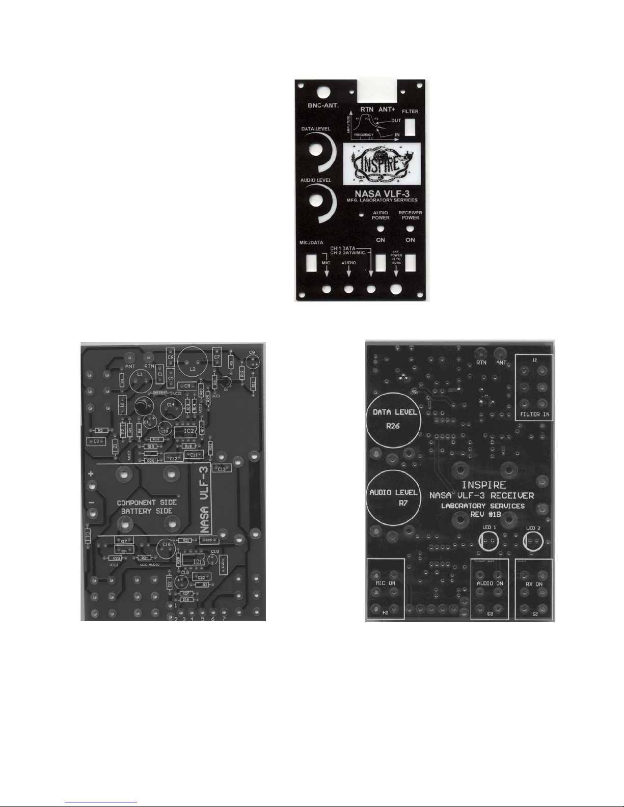
1. Black plastic enclosure
2. Face Plate
3. Printed Circuit Board (PCB)
4. Four bags of components:
Bag 1 resistors, inductors
Bag 2 capacitors
Bag 3 ICs, diodes, sockets
Bag 4 switches, jacks, knobs, antenna terminal, wires, misc. hardware
Page 2
VLF-3 Assembly Instructions
2
Printed Circuit Board (PCB):
Faceplate
Front Control Panel
Component Side / Battery Side
All electronic components are inserted
from this side and soldered on the other
side. The battery holder is inserted
from this side also.
Switch Side
The four DPDT slide switches, the two
10k pots and the two LEDs are inserted
from this side and soldered on the other
side.
Page 3
VLF-3 Assembly Instructions
3
R5
+
–
Page 4
VLF-3 Assembly Instructions
4
ASSEMBLY SEQUENCE
1. Solder components to PCB.
2. Assemble jacks subassembly, connect wires to antenna terminal.
3. Connect wires to PCB.
4. Final assembly of receiver.
5. Test receiver.
(Check off boxes as each step is completed.)
1. Solder components to PCB.
(NOTE: The transistor (Q1) and the field effect transistor (J-FET with ferrite bead) have been
preinstalled.)
1a. Sort and install resistors.
Remove the resistors from Bag 1. Leave the
inductors for later installation.
The colored bands on the resistors indicate the resistance
using a color code. This table indicates how to convert each
color to its numerical equivalent.
0 black
1 brown
2 red
3 orange
4 yellow
5 green
6 blue
7 violet
8 gray
9 white
gold: 5% tolerance.
To read a resistor code, first locate the gold band and
read the colors in order from the other end. (All resistors in
this kit have a gold band indicating 5% tolerance.) The first
two bands indicate digits in the resistance, the third band
(called the multiplier) indicates the number of zeroes to be
added to the digits to obtain the resistance.
(NOTE: 1000 = kilo = k ; 1,000,000 = mega = Meg)
Bag 1 Contents
Resistors:
R1 560 kΩ
R2 10 Ω
R3 2.2 MegΩ
R4 22 MegΩ
R5 680 Ω
R6, R12 220 Ω
(R7, R26 10k pots in Bag #4)
R8 43 kΩ
R9, R17 10 kΩ
R10, R13 2.2 kΩ
R11 470 Ω
R14 100 kΩ
R15, R16, R20 20 kΩ
R18 15 kΩ
R19, R25, R27 100 Ω
R21, R22, R23, R24 1 kΩ
R28 270 kΩ
Inductors
L1 3.9 mH
L2 150 mH
Band 2
Band 3
Band 4
(gold)
Band 1
Page 5
VLF-3 Assembly Instructions
5
What is the resistance for each of the following?
Example 1
Example 2
Example 3
Example 4
Band 1
Band 2
Band 3
brown
black
brown
yellow
violet
orange
red
black
green
orange
orange
orange
Band 1
Band 2
Band 3
1
0
1
4
7
3
2
0
5
3
3
3
Resistance
100
100 Ω
47000
47 kΩ
2000000
2 MegΩ
33000
33 kΩ
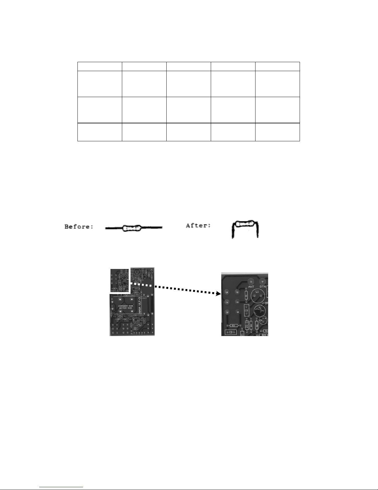
Use the resistor code to identify and sort all of the resistors. One good way to keep them
sorted is to tape one end to a piece of paper and write the resistance and component number (R1,
R2, etc.). Once you have identified and sorted all of the resistors, you are ready to solder them to
the PCB.
To prepare a resistor for insertion into the board, bend the two leads so that they form a
right angle to the resistor body.
Resistor locations on the component side of the PCB are indicated with the “R” number from the
parts list between the two holes for insertion of the leads.
Part of the PCB showing location of R1, R3, R4 and R6.
To install, place the leads of the resistor through the appropriate holes and press the
resistor down against the component side of the PCB. (There is no required orientation for
resistors. Either lead may be inserted in either hole.) Turn the board over while holding the
resistor in position and bend the leads slightly outward to hold the resistor in place and solder the
leads to the circuit side. (NOTE: There will be an empty resistor symbol on the PCB between
R15 and R20. No part will be installed in this location.)
Page 6
VLF-3 Assembly Instructions
6
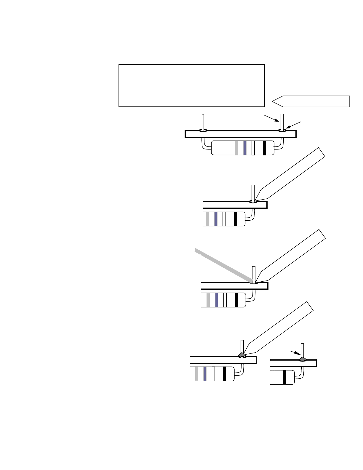
STEPS FOR SOLDERING RESISTORS, CAPACITORS AND WIRES:
IMPORTANT:
DO NOT leave a soldering iron plugged in for
a long time without using it.
NEVER leave a hot soldering iron unattended.
.
PCB
TRIM
PCB
Finished solder joint
Soldering iron
PCB
Touch solder to the side
of the lead away from
the soldering iron.
PCB
lead
contact
PCB
Press soldering iron
firmly down against the
contact and to the side
against the lead.
1. Clean the tip of the iron by wiping it on
the wet sponge.
2. Place a small amount of solder on the
tip.
3. Press the tip down against the circuit
contact and against the resistor lead and
hold for 5 seconds.
4. After the lead and the contact have
heated for 5 seconds, apply the solder to the
lead and contact (NOT directly to the iron)
until the solder melts and flows around the
lead and into the contact.
5. Apply enough solder to allow it to run
down along the lead. Do not apply so
much solder that it runs across the PCB
surface.
6. After enough solder has been applied (12 seconds), remove the solder wire but hold
the iron in place for another 2-3 seconds.
7. Remove the iron, allow the joint to cool
and inspect the joint.
8. Trim the excess lead wire just above the
solder joint.
Repeat this process for the remaining
resistors.
Leave soldering iron in
place for 1-2 more
seconds.
Page 7

VLF-3 Assembly Instructions
7
IMPORTANT Note for New Soldering Irons:
A new soldering iron must be “tinned” in order to work well. Follow these steps:
1. Plug in the iron.
2. When it first heats up, apply solder liberally to the tip.
3. Wipe off the excess solder and you are ready to go!
1b. Install the IC sockets.
Remove the IC sockets and IC1 (LM386) and IC2 (LM358) from Bag #3. When
installing IC sockets and ICs, alignment is very important. One end of the IC symbol on the
PCB has a half-hole at one end of the symbol. One end of the socket has a half-hole. The IC
itself has a circular dot near one end.
Install the sockets so that the half-hole end coincides with the half-hole on the PCB.
Press the sockets firmly against the component side of the PCB. Solder the 8 pins on the other
side of the PCB taking care not to create any solder “bridges” between the pins.
Install the IC so that the end with the dot is at the end of the socket with the half-hole.
Carefully fit the 8 pins in the socket holes and press the IC firmly into the socket.
IC
PCB
HALF HOLE
DOT
Socket
PCB
Page 8

VLF-3 Assembly Instructions
8
1c. Solder capacitors to the PCB.
Capacitor Identification Guide
The small-value ceramic capacitors may be installed
in either orientation, but the larger-value cylindrical
capacitors (C4, C8, C10, C14, C16, C18, C19) must be
installed with the proper polarity.
The polarity is indicated on the PCB by a “+” sign
near one end of the capacitor location.
The polarity is indicated on the body of the
capacitor with a stripe with a minus (-) sign located on the
negative side of the capacitor. Also, the shorter lead is the
negative lead.
To install a capacitor, insert the leads in the
appropriate holes and press the capacitor down near the
PCB. Solder using the same technique as used for resistors.
The polarity is not marked on capacitor C 10.
The proper polarity is indicated here:
NOTE: There may be some variation in capacitor markings due to using different
suppliers.
Bag #2 Contents
Capacitors:
C1, C3 24 pF
C2, C6, C7 .01 µF
C4, C10, C18 10 µF
C5, C9, C13, C15,
C17, C21, C22
C8 1 µF
C11, C12 .001 µF
C14, C16 330 µF
C19 100 µF
C20 .15 µF
}
.1 µF
C11, C12
.001 µF
“102”
C1, C3
24 pF
“240J0”
C2, C6, C7
.01 µF
“103”
C4, C10, C18
10 µF
C8
1 µF
C5
C9
C13
C15
C17
C21
C22
.1 µF
“104”
C14, C16
330 µF
C19
100 µF
C20
.15 µF
“154”
C 10
+
Page 9

VLF-3 Assembly Instructions
9
! 1d. Install the inductors (L1 and L2)
The inductors are the two remaining parts in Bag #1. Inductor L1 is marked “LH 239”..
Inductor L2 is marked “LJ 415”. From the component side, press the inductor firmly down
against the PCB and solder the other side. There is no required polarity for the inductors.
! 1e. Install the diodes from Bag #3.
Polarity is very important in the
installation of diodes.
D1 and D2 are black cylinders with a
silver stripe near one end.
On the PCB, the D1 and D2 locations are shown
as a rectangle with a stripe near one end.
Align the striped end of the diode with
the striped end of the PCB symbol. Press the
diode firmly against the component side of the
PCB and solder the other side.
Z1 and Z2 are small components with a black stripe near one end. The symbol on the
PCB is the same as for D1 and D2. As with D1 and D2, align the black stripe end with the
striped end on the PCB. Press the diodes firmly against the PCB and solder the other side.
Return the LEDs to Bag #3. They will be installed later.
D1
1N
4004
Remaining Bag #3 Contents
D1, D2
Z1, Z2
LED1, LED2
Page 10

VLF-3 Assembly Instructions
10
1f. Install the battery holder.
From Bag #4, take the following parts:
1. Battery holder
2 PCB standoff post
2 4-40 3/8 “ screw
4 4-40 1/4” screw
2 4-40 nuts
2 nylon washers
2 #4 washers
The following diagram shows the assembly of the battery holder to the PCB:
.
1. Place the battery holder
leads through the PCB from
the component side and press
the holder firmly against the
PCB.
2. Insert 1/4” screws through
the holes nearest the leads,
through the PCB and tighten
the nuts on the switch side.
3. Insert 3/8” screws through
the other two holes, through
the PCB, through the nylon
washers and tighten the
standoffs on the switch side.
4. Solder the battery leads on
either (or both) side of the
PCB.
5. Temporarily insert 1/4”
screws through the #4 washers
in the other ends of the
standoffs. These will be used
later to attach to the face plate.
Page 11

VLF-3 Assembly Instructions
11
1f. Install the potentiometer and switches.
From Bag #4, remove the two 10k pots (R7 and R26) and the four DPDT slide switches.
Slide the three contacts for the pots through the holes provided from the switch side of
the PCB. Push the switch firmly against the PCB and solder either (or both) sides.
Insert the six contacts for each DPDT slide switch into position and press the switch
firmly against the switch side of the PCB. Solder each contact on the component side.
1g. Install the LEDs.
R7, R26
DPDT Switches
DPDT
Switches
Align the LED leads as shown with
the shorter lead closest to the line in
the PCB symbol.
Carefully work the LED down as far
as it will go toward the PCB. When
in the proper position, the top of the
LED will be even with the tab on the
adjacent power switch.
Solder the LED leads to either side of
the PCB. Carefully trim the excess
leads.
THIS COMPLETES THE INSTALLATION OF ALL PARTS ON THE PCB!
Page 12

VLF-3 Assembly Instructions
12
2. Attach wires to the PCB.
Bag #4 contains the following wires:
3” red
4” orange
4” yellow
3” blue
3” black
5” white
Make the following cuts on the wires:
1 red: 1”, 2”
1 orange: 2”, 2”
1 yellow: 2”, 2”
1 blue: 3”
1 black: 1”, 2”
1 white: 2”, 1.5”, 1.5”
To prepare a wire for soldering, strip about 1/8” of insulation from each end. To solder a wire to
the PCB:
1. insert the wire into the component side,
2. press the soldering iron to the wire and to the metal pad on the PCB
for about 5 seconds to heat both the wire and the pad,
3. apply solder to the side away from the soldering iron making sure
that the wire and pad melt the solder, not the soldering iron.
Solder the 1” red wire to the ANT connection on the PCB.
Solder the 1” black wire to the RTN connection on the PCB
The wire connections to the PCB are numbered 1-7.
Connect the following wires to the appropriate locations:
Connection 1: 2” red wire
Connection 2: 2” black wire and 2” white wire twisted together
Connection 3: 2” orange wire
Connection 4: 2” orange wire
Connection 5: 2” yellow wire
Connection 6: 2” yellow wire
Connection 7: 3” blue wire
See also the photos on the following page.
ANT
RTN
Page 13

VLF-3 Assembly Instructions
13
Wires installed (component-side view)
Wires installed (switch-side view)
Close up of white and black wire
twisted together prior to being
soldered to location #2 on the PCB.
Page 14

VLF-3 Assembly Instructions
14
3. Install the jacks and connectors to the faceplate.
Install the jacks and the external power connector to the faceplate by inserting them from the
back side and tightening the knurled nut on the front side. Mount the 2-screw antenna terminal
to the faceplate by placing the terminal in front of the faceplate and using the two remaining 4-40
1/4” screws and nuts. Mount the BNC connector by removing the nut and washer, inserting the
connector from the front of the panel and tightening the nut over the washer.
4. Attach the PCB to the faceplate.
Remove the nuts and washers from the standoffs and the nuts from the shafts of the 10k pots.
Attach the faceplate to the PCB by fitting the faceplate over the switches and LEDs. Tighten the
screws and washers to the standoffs. Tighten the nuts on the 10k pot shafts.
5. Solder wires to jacks and connectors.
To solder the wire to a jack contact:
1. insert the wire through the hole in the tab,
2. press the soldering iron to both the wire and the tab and heat for
5 seconds,
3. apply the solder to the side away from the soldering iron, making
sure that the wire and tab melt the solder, not the iron.
Use the following figure as a guide for wiring connections to the jacks and the external power
connector. See also the photo on the next page.
The monaural jack
(white body) is the
MIC jack. The
blue wire connects
to this jack.
The center two are
the Audio and
Data jacks and are
the black body
stereo type.
The round one is
the external power
connector.
White
White
White
MIC
AUDIO
DATA
POWER
Yellow
Blue
Orange
Orange
Black
Red
Yellow
NOTES:
1. The yellow and orange wires must cross to reach
the correct jacks.
2. The white ground wire and the black wire both
connect to Location 2.
Page 15

VLF-3 Assembly Instructions
15
Close-up showing wires soldered to the jack tabs.
NOTE: The orange and yellow wires must cross to connect to the appropriate jacks.
The microphone connector may be either white (as pictured) or black
Front view of completed
VLF-3 receiver
Page 16

VLF-3 Assembly Instructions
16
Solder the black “RTN” wire to the RTN side of the antenna
terminal.
Insert the red wire into the BNC connector and solder in place.
Solder both red wires to the “ANT+” side of the antenna terminal.
Use the set screws to attach the knobs to the 10k pot shafts.
Install a 9-volt battery in the battery holder.
Use the 4 6/32 1/4 inch screws to attach the faceplate to the
enclosure
THIS COMPLETES THE ASSEMBLY OF YOUR VLF-3 RECEIVER!
! 6. Test your receiver.
Attach an antenna to the ANT+ terminal. A 1-2 meter piece of wire will do.
Attach a ground to the RTN terminal. A short wire that you hold in your hand will do.
Antenna Terminal
Antenna
Ground
Microphone
Headphones
Stereo cable
Page 17

VLF-3 Assembly Instructions
17
6a. Test the audio output.
Plug some headphones in the audio output jack.
Turn on the “RECEIVER POWER” switch (main power switch).
Turn on the “AUDIO POWER” switch and slowly turn the “AUDIO LEVEL” up.
You should hear a loud hum as you pick up the 60 hertz signal given off by building
wiring.
6b. Test the data output.
Connect the “DATA” output jack with the microphone input of the cassette recorder
using a stereo cable.
Connect headphones to the recorder.
Put a tape in the recorder and press “RECORD”. (Put the recorder on “PAUSE” if you
do not want tape running during this test.)
Turn on the “RECEIVER POWER” switch and slowly turn the “DATA LEVEL” up.
You should hear the same signal as you did through the audio output.
Plug a microphone into the MIC IN jack. Slide the switch to the MIC. position. You
should hear the 60 hertz hum in one ear and the microphone input in the other ear.
6c. Field test your receiver.
To ready your receiver for field testing, you will need a better antenna and a better
ground.
A good antenna is a 72-inch collapsible antenna available from Pacific Antenna for
$10 plus shipping. (http://www.pacificantenna.com/Ordering.htm)
A 2 meter length of sturdy wire will work almost as well but is slightly less easy to
transport.
A good ground is a metal stake or pipe driven into the ground. Attaching a wire from the
ground terminal to the stake will provide a good ground. Attaching a wire from the
ground terminal to the body of a car (a counterpoise) will work also. In a pinch, you can
touch the ground terminal and use your body as a ground.
If you hear a loud squeal as the output, check the output level and the ground
connections.
Page 18

VLF-3 Assembly Instructions
18
NOTE:
Caution should be used in identifying R3 (2.2 MegΩ) and R4 (22 MegΩ). The green band and
the blue band can look similar. For best results, identify both components together so
differences can be noted.
Loose connection joints are often the cause of the receiver not functioning properly. Checking to
make sure there is a firm connection and adding a good solder joint on both sides of the board
will help eliminate this problem.
Any part shortages or discrepancies should be reported to the inspire project:
president@TheINSPIREProject.org
Any corrections, suggestions or recommendations for improvement of the assembly instructions
would also be appreciated.
Thank you for your participation and support of The INSPIRE Project!
 Loading...