


8-Bit
XC886/888CLM
8-Bit Single Chip Microcontroller
Data Sheet
V1.2 2009-07
Microcontrollers

Edition 2009-07
Published by
Infineon Technologies AG
81726 Munich, Germany
© 2009 Infineon Technologies AG
All Rights Reserved.
Legal Disclaimer
The information given in this document shall in no event be regarded as a guarantee of conditions or
characteristics. With respect to any examples or hints given herein, any typical values stated herein and/or any
information regarding the application of the device, Infineon Technologies hereby disclaims any and all warranties
and liabilities of any kind, including without limitation, warranties of non-infringement of intellectual property rights
of any third party.
Information
For further information on technology, delivery terms and conditions and prices, please contact the nearest
Infineon Technologies Office (www.infineon.com).
Warnings
Due to technical requirements, components may contain dangerous substances. For information on the types in
question, please contact the nearest Infineon Technologies Office.
Infineon Technologies components may be used in life-support devices or systems only with the express written
approval of Infineon Technologies, if a failure of such components can reasonably be expected to cause the failure
of that life-support device or system or to affect the safety or effectiveness of that device or system. Life support
devices or systems are intended to be implanted in the human body or to support and/or maintain and sustain
and/or protect human life. If they fail, it is reasonable to assume that the health of the user or other persons may
be endangered.

8-Bit
XC886/888CLM
8-Bit Single Chip Microcontroller
Data Sheet
V1.2 2009-07
Microcontrollers

XC886/888CLM
XC886/888 Data Sheet
Revision History: V1.2 2009-07
Previous Versions: V1.0, V1.1
Page Subjects (major changes since last revision)
Changes from V1.1 2009-01 to V1.2 2009-07
89 Note on LIN baud rate detection is added.
92 RXD slave line in SSC block diagram is updated.
108 Electrical parameters are now valid for all variants, previous note on
exclusion of ROM variants is removed.
116 Symbol for ADC error parameters are updated.
120 Power supply current parameters for ROM variants are updated.
128 Test condition for the on-chip oscillator short term deviation is updated.
We Listen to Your Comments
Any information within this document that you feel is wrong, unclear or missing at all?
Your feedback will help us to continuously improve the quality of this document.
Please send your proposal (including a reference to this document) to:
mcdocu.comments@infineon.com
Data Sheet V1.2, 2009-07

XC886/888CLM
Table of Contents
Table of Contents
1 Summary of Features . . . . . . . . . . . . . . . . . . . . . . . . . . . . . . . . . . . . . . . . 1
2 General Device Information . . . . . . . . . . . . . . . . . . . . . . . . . . . . . . . . . . . 5
2.1 Block Diagram . . . . . . . . . . . . . . . . . . . . . . . . . . . . . . . . . . . . . . . . . . . . . . . 5
2.2 Logic Symbol . . . . . . . . . . . . . . . . . . . . . . . . . . . . . . . . . . . . . . . . . . . . . . . . 6
2.3 Pin Configuration . . . . . . . . . . . . . . . . . . . . . . . . . . . . . . . . . . . . . . . . . . . . . 7
2.4 Pin Definitions and Functions . . . . . . . . . . . . . . . . . . . . . . . . . . . . . . . . . . . 9
3 Functional Description . . . . . . . . . . . . . . . . . . . . . . . . . . . . . . . . . . . . . . 19
3.1 Processor Architecture . . . . . . . . . . . . . . . . . . . . . . . . . . . . . . . . . . . . . . . 19
3.2 Memory Organization . . . . . . . . . . . . . . . . . . . . . . . . . . . . . . . . . . . . . . . . 20
3.2.1 Memory Protection Strategy . . . . . . . . . . . . . . . . . . . . . . . . . . . . . . . . . 21
3.2.1.1 Flash Memory Protection . . . . . . . . . . . . . . . . . . . . . . . . . . . . . . . . . . 21
3.2.2 Special Function Register . . . . . . . . . . . . . . . . . . . . . . . . . . . . . . . . . . . 23
3.2.2.1 Address Extension by Mapping . . . . . . . . . . . . . . . . . . . . . . . . . . . . . 23
3.2.2.2 Address Extension by Paging . . . . . . . . . . . . . . . . . . . . . . . . . . . . . . 25
3.2.3 Bit Protection Scheme . . . . . . . . . . . . . . . . . . . . . . . . . . . . . . . . . . . . . . 29
3.2.3.1 Password Register . . . . . . . . . . . . . . . . . . . . . . . . . . . . . . . . . . . . . . . 30
3.2.4 XC886/888 Register Overview . . . . . . . . . . . . . . . . . . . . . . . . . . . . . . . 31
3.2.4.1 CPU Registers . . . . . . . . . . . . . . . . . . . . . . . . . . . . . . . . . . . . . . . . . . 31
3.2.4.2 MDU Registers . . . . . . . . . . . . . . . . . . . . . . . . . . . . . . . . . . . . . . . . . 32
3.2.4.3 CORDIC Registers . . . . . . . . . . . . . . . . . . . . . . . . . . . . . . . . . . . . . . 33
3.2.4.4 System Control Registers . . . . . . . . . . . . . . . . . . . . . . . . . . . . . . . . . 34
3.2.4.5 WDT Registers . . . . . . . . . . . . . . . . . . . . . . . . . . . . . . . . . . . . . . . . . 36
3.2.4.6 Port Registers . . . . . . . . . . . . . . . . . . . . . . . . . . . . . . . . . . . . . . . . . . 37
3.2.4.7 ADC Registers . . . . . . . . . . . . . . . . . . . . . . . . . . . . . . . . . . . . . . . . . . 39
3.2.4.8 Timer 2 Registers . . . . . . . . . . . . . . . . . . . . . . . . . . . . . . . . . . . . . . . 43
3.2.4.9 Timer 21 Registers . . . . . . . . . . . . . . . . . . . . . . . . . . . . . . . . . . . . . . 43
3.2.4.10 CCU6 Registers . . . . . . . . . . . . . . . . . . . . . . . . . . . . . . . . . . . . . . . . . 44
3.2.4.11 UART1 Registers . . . . . . . . . . . . . . . . . . . . . . . . . . . . . . . . . . . . . . . . 48
3.2.4.12 SSC Registers . . . . . . . . . . . . . . . . . . . . . . . . . . . . . . . . . . . . . . . . . . 49
3.2.4.13 MultiCAN Registers . . . . . . . . . . . . . . . . . . . . . . . . . . . . . . . . . . . . . . 49
3.2.4.14 OCDS Registers . . . . . . . . . . . . . . . . . . . . . . . . . . . . . . . . . . . . . . . . 50
3.3 Flash Memory . . . . . . . . . . . . . . . . . . . . . . . . . . . . . . . . . . . . . . . . . . . . . . 52
3.3.1 Flash Bank Sectorization . . . . . . . . . . . . . . . . . . . . . . . . . . . . . . . . . . . . 53
3.3.2 Parallel Read Access of P-Flash . . . . . . . . . . . . . . . . . . . . . . . . . . . . . . 54
3.3.3 Flash Programming Width . . . . . . . . . . . . . . . . . . . . . . . . . . . . . . . . . . . 55
3.4 Interrupt System . . . . . . . . . . . . . . . . . . . . . . . . . . . . . . . . . . . . . . . . . . . . 56
3.4.1 Interrupt Source . . . . . . . . . . . . . . . . . . . . . . . . . . . . . . . . . . . . . . . . . . . 56
3.4.2 Interrupt Source and Vector . . . . . . . . . . . . . . . . . . . . . . . . . . . . . . . . . . 62
3.4.3 Interrupt Priority . . . . . . . . . . . . . . . . . . . . . . . . . . . . . . . . . . . . . . . . . . . 64
3.5 Parallel Ports . . . . . . . . . . . . . . . . . . . . . . . . . . . . . . . . . . . . . . . . . . . . . . . 65
Data Sheet I-1 V1.2, 2009-07

XC886/888CLM
Table of Contents
3.6 Power Supply System with Embedded Voltage Regulator . . . . . . . . . . . . 68
3.7 Reset Control . . . . . . . . . . . . . . . . . . . . . . . . . . . . . . . . . . . . . . . . . . . . . . . 69
3.7.1 Module Reset Behavior . . . . . . . . . . . . . . . . . . . . . . . . . . . . . . . . . . . . . 71
3.7.2 Booting Scheme . . . . . . . . . . . . . . . . . . . . . . . . . . . . . . . . . . . . . . . . . . 71
3.8 Clock Generation Unit . . . . . . . . . . . . . . . . . . . . . . . . . . . . . . . . . . . . . . . . 72
3.8.1 Recommended External Oscillator Circuits . . . . . . . . . . . . . . . . . . . . . . 75
3.8.2 Clock Management . . . . . . . . . . . . . . . . . . . . . . . . . . . . . . . . . . . . . . . . 77
3.9 Power Saving Modes . . . . . . . . . . . . . . . . . . . . . . . . . . . . . . . . . . . . . . . . . 79
3.10 Watchdog Timer . . . . . . . . . . . . . . . . . . . . . . . . . . . . . . . . . . . . . . . . . . . . 80
3.11 Multiplication/Division Unit . . . . . . . . . . . . . . . . . . . . . . . . . . . . . . . . . . . . . 83
3.12 CORDIC Coprocessor . . . . . . . . . . . . . . . . . . . . . . . . . . . . . . . . . . . . . . . . 84
3.13 UART and UART1 . . . . . . . . . . . . . . . . . . . . . . . . . . . . . . . . . . . . . . . . . . . 85
3.13.1 Baud-Rate Generator . . . . . . . . . . . . . . . . . . . . . . . . . . . . . . . . . . . . . . 85
3.13.2 Baud Rate Generation using Timer 1 . . . . . . . . . . . . . . . . . . . . . . . . . . 88
3.14 Normal Divider Mode (8-bit Auto-reload Timer) . . . . . . . . . . . . . . . . . . . . . 88
3.15 LIN Protocol . . . . . . . . . . . . . . . . . . . . . . . . . . . . . . . . . . . . . . . . . . . . . . . . 89
3.15.1 LIN Header Transmission . . . . . . . . . . . . . . . . . . . . . . . . . . . . . . . . . . . 89
3.16 High-Speed Synchronous Serial Interface . . . . . . . . . . . . . . . . . . . . . . . . . 91
3.17 Timer 0 and Timer 1 . . . . . . . . . . . . . . . . . . . . . . . . . . . . . . . . . . . . . . . . . 93
3.18 Timer 2 and Timer 21 . . . . . . . . . . . . . . . . . . . . . . . . . . . . . . . . . . . . . . . . 94
3.19 Capture/Compare Unit 6 . . . . . . . . . . . . . . . . . . . . . . . . . . . . . . . . . . . . . . 95
3.20 Controller Area Network (MultiCAN) . . . . . . . . . . . . . . . . . . . . . . . . . . . . . 97
3.21 Analog-to-Digital Converter . . . . . . . . . . . . . . . . . . . . . . . . . . . . . . . . . . . . 99
3.21.1 ADC Clocking Scheme . . . . . . . . . . . . . . . . . . . . . . . . . . . . . . . . . . . . . 99
3.21.2 ADC Conversion Sequence . . . . . . . . . . . . . . . . . . . . . . . . . . . . . . . . . 101
3.22 On-Chip Debug Support . . . . . . . . . . . . . . . . . . . . . . . . . . . . . . . . . . . . . 102
3.22.1 JTAG ID Register . . . . . . . . . . . . . . . . . . . . . . . . . . . . . . . . . . . . . . . . . 103
3.23 Chip Identification Number . . . . . . . . . . . . . . . . . . . . . . . . . . . . . . . . . . . 104
4 Electrical Parameters . . . . . . . . . . . . . . . . . . . . . . . . . . . . . . . . . . . . . . 108
4.1 General Parameters . . . . . . . . . . . . . . . . . . . . . . . . . . . . . . . . . . . . . . . . 108
4.1.1 Parameter Interpretation . . . . . . . . . . . . . . . . . . . . . . . . . . . . . . . . . . . 108
4.1.2 Absolute Maximum Rating . . . . . . . . . . . . . . . . . . . . . . . . . . . . . . . . . . 109
4.1.3 Operating Conditions . . . . . . . . . . . . . . . . . . . . . . . . . . . . . . . . . . . . . . 110
4.2 DC Parameters . . . . . . . . . . . . . . . . . . . . . . . . . . . . . . . . . . . . . . . . . . . . 111
4.2.1 Input/Output Characteristics . . . . . . . . . . . . . . . . . . . . . . . . . . . . . . . . 111
4.2.2 Supply Threshold Characteristics . . . . . . . . . . . . . . . . . . . . . . . . . . . . 115
4.2.3 ADC Characteristics . . . . . . . . . . . . . . . . . . . . . . . . . . . . . . . . . . . . . . 116
4.2.3.1 ADC Conversion Timing . . . . . . . . . . . . . . . . . . . . . . . . . . . . . . . . . 119
4.2.4 Power Supply Current . . . . . . . . . . . . . . . . . . . . . . . . . . . . . . . . . . . . . 120
4.3 AC Parameters . . . . . . . . . . . . . . . . . . . . . . . . . . . . . . . . . . . . . . . . . . . . 124
4.3.1 Testing Waveforms . . . . . . . . . . . . . . . . . . . . . . . . . . . . . . . . . . . . . . . 124
4.3.2 Output Rise/Fall Times . . . . . . . . . . . . . . . . . . . . . . . . . . . . . . . . . . . . 125
Data Sheet I-2 V1.2, 2009-07

XC886/888CLM
Table of Contents
4.3.3 Power-on Reset and PLL Timing . . . . . . . . . . . . . . . . . . . . . . . . . . . . . 126
4.3.4 On-Chip Oscillator Characteristics . . . . . . . . . . . . . . . . . . . . . . . . . . . . 128
4.3.5 External Clock Drive XTAL1 . . . . . . . . . . . . . . . . . . . . . . . . . . . . . . . . 129
4.3.6 JTAG Timing . . . . . . . . . . . . . . . . . . . . . . . . . . . . . . . . . . . . . . . . . . . . 130
4.3.7 SSC Master Mode Timing . . . . . . . . . . . . . . . . . . . . . . . . . . . . . . . . . . 132
5 Package and Quality Declaration . . . . . . . . . . . . . . . . . . . . . . . . . . . . . 133
5.1 Package Parameters . . . . . . . . . . . . . . . . . . . . . . . . . . . . . . . . . . . . . . . . 133
5.2 Package Outline . . . . . . . . . . . . . . . . . . . . . . . . . . . . . . . . . . . . . . . . . . . 134
5.3 Quality Declaration . . . . . . . . . . . . . . . . . . . . . . . . . . . . . . . . . . . . . . . . . 136
Data Sheet I-3 V1.2, 2009-07
XC886/888CLM8-Bit Single Chip Microcontroller
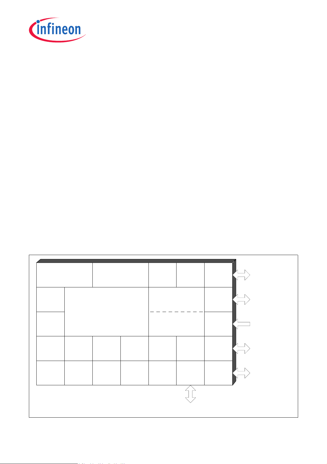
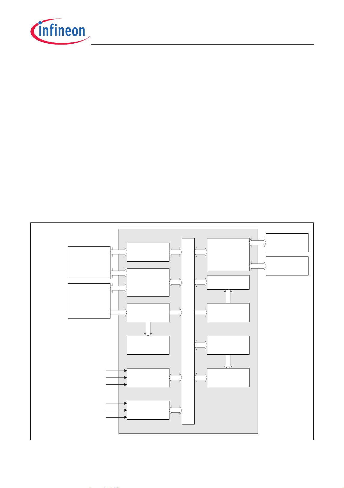
1 Summary of Features
The XC886/888 has the following features:
• High-performance XC800 Core
– compatible with standard 8051 processor
– two clocks per machine cycle architecture (for memory access without wait state)
– two data pointers
• On-chip memory
– 12 Kbytes of Boot ROM
– 256 bytes of RAM
– 1.5 Kbytes of XRAM
– 24/32 Kbytes of Flash; or
24/32 Kbytes of ROM, with additional 4 Kbytes of Flash
(includes memory protection strategy)
• I/O port supply at 3.3 V or 5.0 V and core logic supply at 2.5 V (generated by
embedded voltage regulator)
(more features on next page)
Flash or ROM
24K/32K x 8
Boot ROM
12K x 8
XRAM
1.5K x 8
RAM
256 x 8
1) All ROM devices come with an additional 4K x 8 Flash
1)
Timer 0
16-bit
On-Chip Debug Support
XC800 Core
Timer 1
16-bit
Timer 2
16-bit
Timer 21
16-bit
UART
Capture/Compare Unit
Compare Unit
Watchdog
Timer
UART1
SSC
16-bit
16-bit
ADC
10-bit
8-channel
8-bit Digital I/O
Port 0
Port 1
Port 2
Port 3
Port 4Port 5MDU CORDIC MultiCAN
8-bit Digital I/O
8-bit Digital I/O
8-bit Digital/
Analog Input
8-bit Digital I/O
8-bit Digital I/O
.
Figure 1 XC886/888 Functional Units
Data Sheet 1 V1.2, 2009-07

XC886/888CLM
Summary of Features
Features: (continued)
• Power-on reset generation
• Brownout detection for core logic supply
• On-chip OSC and PLL for clock generation
– PLL loss-of-lock detection
• Power saving modes
– slow-down mode
– idle mode
– power-down mode with wake-up capability via RXD or EXINT0
– clock gating control to each peripheral
• Programmable 16-bit Watchdog Timer (WDT)
•Six ports
– Up to 48 pins as digital I/O
– 8 pins as digital/analog input
• 8-channel, 10-bit ADC
• Four 16-bit timers
– Timer 0 and Timer 1 (T0 and T1)
– Timer 2 and Timer 21 (T2 and T21)
• Multiplication/Division Unit for arithmetic operations (MDU)
• Software libraries to support floating point and MDU calculations
• CORDIC Coprocessor for computation of trigonometric, hyperbolic and linear
functions
• MultiCAN with 2 nodes, 32 message objects
• Capture/compare unit for PWM signal generation (CCU6)
• Two full-duplex serial interfaces (UART and UART1)
• Synchronous serial channel (SSC)
• On-chip debug support
– 1 Kbyte of monitor ROM (part of the 12-Kbyte Boot ROM)
– 64 bytes of monitor RAM
• Packages:
– PG-TQFP-48
– PG-TQFP-64
T
• Temperature range
– SAF (-40 to 85 °C)
– SAK (-40 to 125 °C)
:
A
Data Sheet 2 V1.2, 2009-07
XC886/888CLM
Summary of Features
XC886/888 Variant Devices
The XC886/888 product family features devices with different configurations, program
memory sizes, package options, power supply voltage, temperature and quality profiles
(Automotive or Industrial), to offer cost-effective solutions for different application
requirements.
The list of XC886/888 device configurations are summarized in Table 1. For each
configuration, 2 types of packages are available:
• PG-TQFP-48, which is denoted by XC886 and;
• PG-TQFP-64, which is denoted by XC888.
Table 1 Device Configuration
Device Name CAN
Module
LIN BSL
Support
MDU
Module
XC886/888 No No No
XC886/888C Yes No No
XC886/888CM Yes No Yes
XC886/888LM No Yes Yes
XC886/888CLM Yes Yes Yes
Note: For variants with LIN BSL support, only LIN BSL is available regardless of the
availability of the CAN module.
From these 10 different combinations of configuration and package type, each are
further made available in many sales types, which are grouped according to device type,
program memory sizes, power supply voltage, temperature and quality profile
(Automotive or Industrial), as shown in Table 2.
Table 2 Device Profile
Sales Type Device
Type
Program
Memory
(Kbytes)
Power
Supply
(V)
Temperature
(°C)
Quality
Profile
SAK-XC886*/888*-8FFA 5V Flash 32 5.0 -40 to 125 Automotive
SAK-XC886*/888*-6FFA 5V Flash 24 5.0 -40 to 125 Automotive
SAF-XC886*/888*-8FFA 5V Flash 32 5.0 -40 to 85 Automotive
SAF-XC886*/888*-6FFA 5V Flash 24 5.0 -40 to 85 Automotive
SAF-XC886*/888*-8FFI 5V Flash 32 5.0 -40 to 85 Industrial
SAF-XC886*/888*-6FFI 5V Flash 24 5.0 -40 to 85 Industrial
Data Sheet 3 V1.2, 2009-07
Table 2 Device Profile (cont’d)
XC886/888CLM
Summary of Features
Sales Type Device
Type
Program
Memory
(Kbytes)
Power
Supply
(V)
Temperature
(°C)
Quality
Profile
SAK-XC886*/888*-8FFA 3V3 Flash 32 3.3 -40 to 125 Automotive
SAK-XC886*/888*-6FFA 3V3 Flash 24 3.3 -40 to 125 Automotive
SAF-XC886*/888*-8FFA 3V3 Flash 32 3.3 -40 to 85 Automotive
SAF-XC886*/888*-6FFA 3V3 Flash 24 3.3 -40 to 85 Automotive
SAF-XC886*/888*-8FFI 3V3 Flash 32 3.3 -40 to 85 Industrial
SAF-XC886*/888*-6FFI 3V3 Flash 24 3.3 -40 to 85 Industrial
Note: The asterisk (*) above denotes the device configuration letters from Table 1.
Corresponding ROM derivatives will be available on request.
Note: For variants with LIN BSL support, only LIN BSL is available regardless of the
availability of the CAN module.
As this document refers to all the derivatives, some description may not apply to a
specific product. For simplicity, all versions are referred to by the term XC886/888
throughout this document.
Ordering Information
The ordering code for Infineon Technologies microcontrollers provides an exact
reference to the required product. This ordering code identifies:
• The derivative itself, i.e. its function set, the temperature range, and the supply
voltage
• The package and the type of delivery
For the available ordering codes for the XC886/888, please refer to your responsible
sales representative or your local distributor.
Note: The ordering codes for the Mask-ROM versions are defined for each product after
verification of the respective ROM code.
Data Sheet 4 V1.2, 2009-07
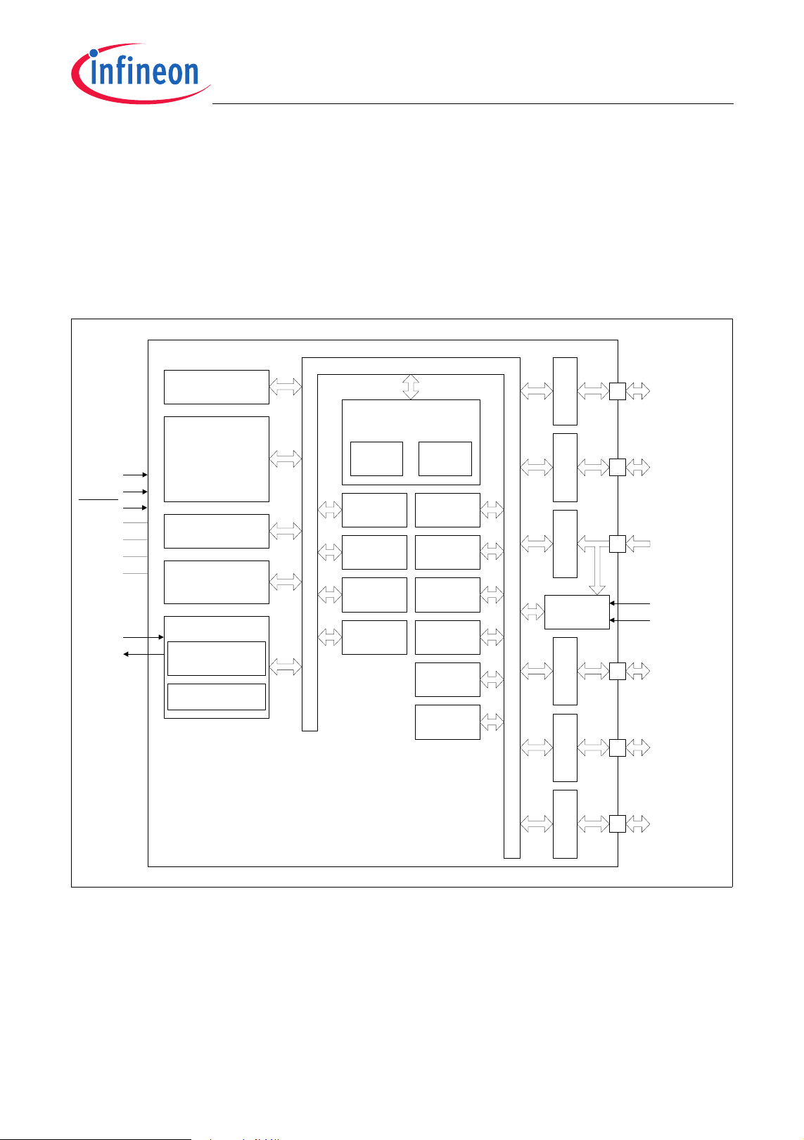
XC886/888CLM
General Device Information
2 General Device Information
Chapter 2 contains the block diagram, pin configurations, definitions and functions of the
XC886/888.
2.1 Block Diagram
The block diagram of the XC886/888 is shown in Figure 2.
TMS
MBC
RESET
V
DDP
V
SSP
V
DDC
V
SSC
XTAL1
XTAL2
XC886/888
12-Kbyte
Boot ROM
256-byte RAM
64-byte monitor
1.5-Kbyte XRAM
24/32-Kbyte
Flash or ROM
Clock Generator
9.6 MHz
On-chip OSC
1)
+
RAM
PLL
Internal Bus
XC800 Core
T0 & T1 UART
UART1CORDIC
SSCMDU
2)
WDT
OCDS
Timer 2
Timer 21
CCU6
MultiCAN
Port 0Port 1Port 2Port 3
ADC
Port 4Port 5
P0.0 - P0.7
P1.0 - P1.7
P2.0 - P2.7
V
AREF
V
AGND
P3.0 - P3.7
P4.0 - P4.7
1) Includes 1-Kbyte monitor ROM
P5.0 - P5.7
2) The 24/32-Kbyte ROM has an additional 4-Kbyte Flash
Figure 2 XC886/888 Block Diagram
Data Sheet 5 V1.2, 2009-07
General Device Information
t
t
t
t
t
t
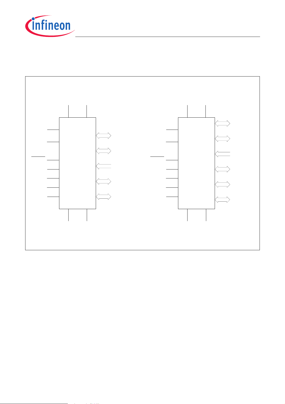
2.2 Logic Symbol
The logic symbols of the XC886/888 are shown in Figure 3.
XC886/888CLM
V
AREF
V
AGND
RESET
MBC
TMS
XTAL1
XTAL2
V
V
DDP
XC886
DDC
V
SSP
V
DDP
V
SSP
Port 0 8-Bi
V
Port 0 7-Bit
Port 1 8-Bit
Port 2 8-Bit
Port 3 8-Bit
Port 4 3-Bit
V
SSC
AREF
V
AGND
RESET
MBC
TMS
XTAL1
XTAL2
V
DDC
XC888
Port 1 8-Bi
Port 2 8-Bi
Port 3 8-Bi
Port 4 8-Bi
Port 5 8-Bi
V
SSC
Figure 3 XC886/888 Logic Symbol
Data Sheet 6 V1.2, 2009-07
XC886/888CLM
General Device Information
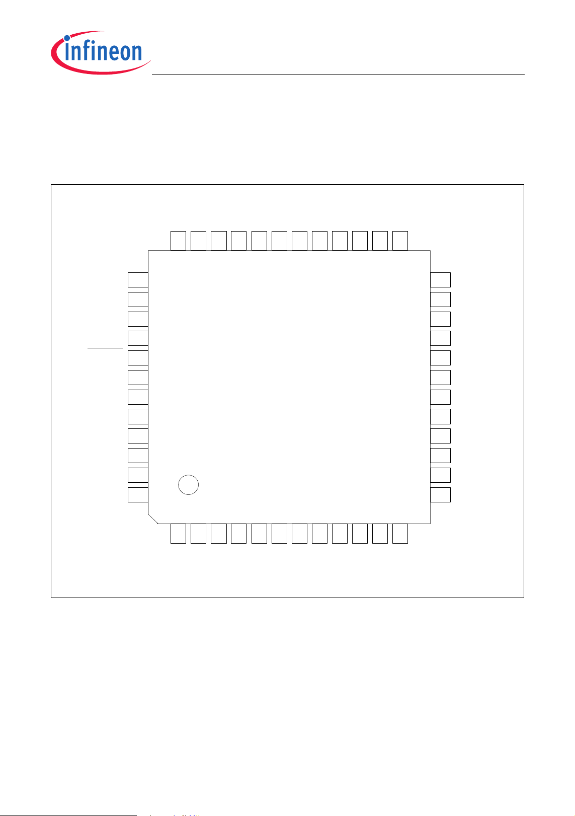
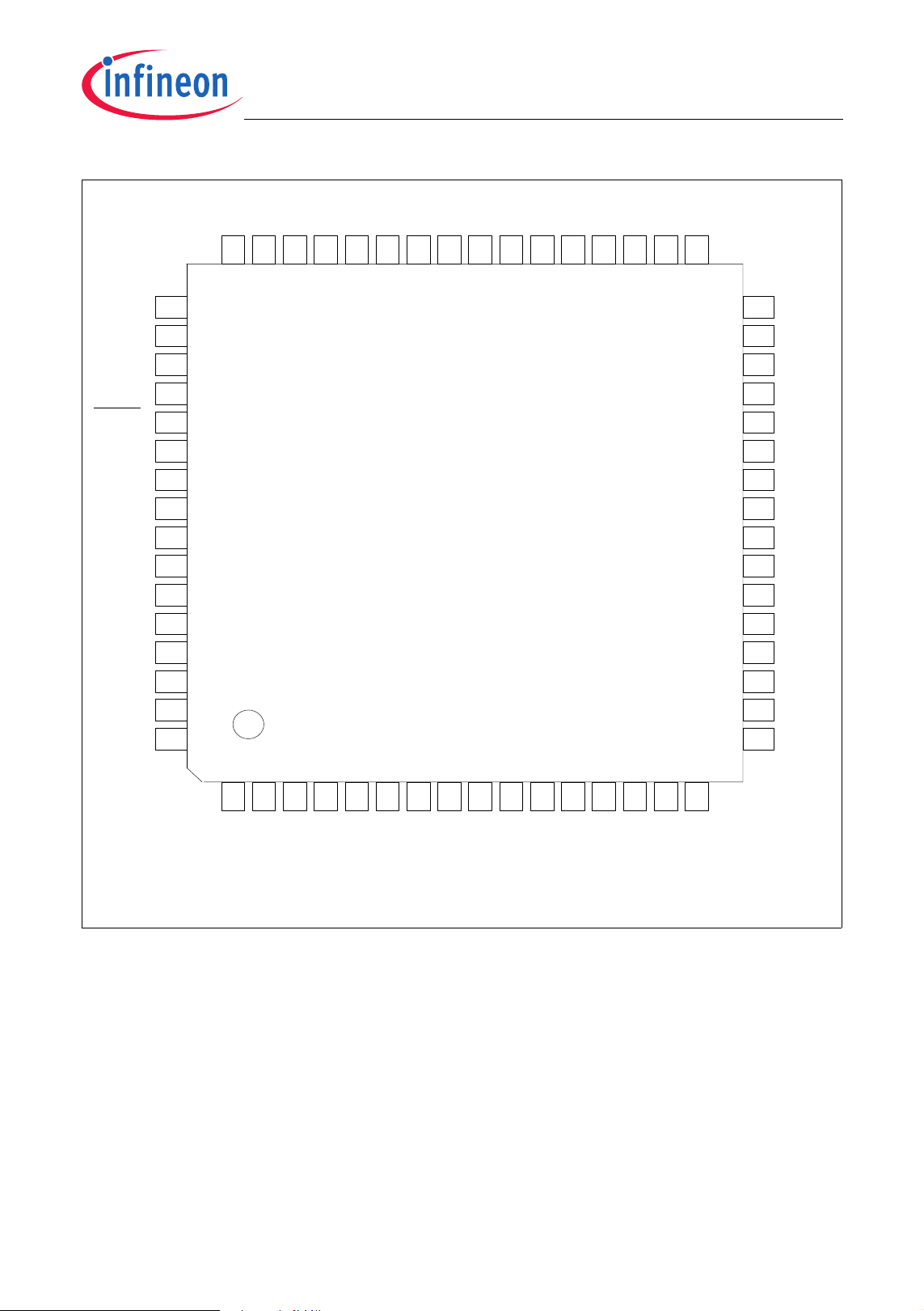
2.3 Pin Configuration
The pin configuration of the XC886, which is based on the PG-TQFP-48 package, is
shown in
package, is shown in Figure 5.
Figure 4, while that of the XC888, which is based on the PG-TQFP-64
P1.3
P1.4
P3.0
P3.1
P3.6
P3.7
P1.5
P4.3
36 35 34 33 32 31 30 29 28 27 26 25
P1.2
P1.0
P1.1
P2.7
P3.2
P3.3
P3.4
P3.5
RESET
V
SSP
V
DDP
MBC
P4.0
P4.1
P0.7
P0.3
37
38
39
40
41
42
XC886
43
44
45
46
47
48
123 456789101112
P0. 4
P0. 5
XTA L2
XTA L1
V
SSCVDDC
P1. 6
P1. 7
V
DDP
TMS
24
23
22
21
20
19
18
17
16
15
14
13
P0. 0
P0. 2
V
AREF
V
AGND
P2.6
P2.5
P2.4
P2.3
V
SSP
V
DDP
P2.2
.
P
2
P2.0
.
P
0
1
1
Figure 4 XC886 Pin Configuration, PG-TQFP-48 Package (top view)
Data Sheet 7 V1.2, 2009-07
XC886/888CLM
General Device Information
P1.3
P1.4
P3.0
P4.5
P4.6
P4.7
P3.1
P4.4
P3.6
P3.7
P1.5
P4.3
48 47 46 45 44 43 42 41 40 39 38 37 36 35 34 33
P1.2
P1.0
P1.1
P2.7
P3.2
P3.3
P3.4
P3.5
RESET
V
SSP
V
DDP
NC
NC
MBC
P4.0
P4.1
P4.2
P0.7
P0.3
P0.4
49
50
51
52
53
54
55
56
XC888
57
58
59
60
61
62
63
64
1 2 3 4 5 6 7 8 9 10111213141516
32
31
30
29
28
27
26
25
24
23
22
21
20
19
18
17
V
AREF
V
AGND
P2.6
P2.5
P2.4
P2.3
V
SSP
V
DDP
P2.2
2
P
P2.0
0
P
P5.7
P5.6
P0.2
P0.0
.
1
.
1
V
P5.0
P0.5
XTA L2
P0.6
XTA L1
V
SSCVDDC
DDP
P5.1
P1.6
P1.7
P5.2
P5.4
P5.3
TMS
P5.5
Note: The pi ns shaded in blue are not av ailable in the PG-TQFP -48 package.
Figure 5 XC888 Pin Configuration, PG-TQFP-64 Package (top view)
Data Sheet 8 V1.2, 2009-07
XC886/888CLM
General Device Information
2.4 Pin Definitions and Functions
The functions and default states of the XC886/888 external pins are provided in Table 3.
Table 3 Pin Definitions and Functions
Symbol Pin Number
(TQFP-48/64)
Type Reset
State
Function
P0 I/O Port 0
Port 0 is an 8-bit bidirectional general purpose
I/O port. It can be used as alternate functions
for the JTAG, CCU6, UART, UART1, Timer
Timer
P0.0 11/17 Hi-Z TCK_0
T12HR_1
CC61_1
CLKOUT_0
RXDO_1
P0.1 13/21 Hi-Z TDI_0
T13HR_1
RXD_1
RXDC1_0
COUT61_1
EXF2_1
2,
21, MultiCAN and SSC.
JTAG Clock Input
CCU6 Timer 12 Hardware Run
Input
Input/Output of
Capture/Compare channel 1
Clock Output
UART Transmit Data Output
JTAG Serial Data Input
CCU6 Timer 13 Hardware Run
Input
UART Receive Data Input
MultiCAN Node 1 Receiver Input
Output of Capture/Compare
channel 1
Timer 2 External Flag Output
P0.2 12/18 PU CTRAP_2
TDO_0
TXD_1
CCU6 Trap Input
JTAG Serial Data Output
UART Transmit Data
Output/Clock Output
TXDC1_0
MultiCAN Node 1 Transmitter
Output
P0.3 48/63 Hi-Z SCK_1
COUT63_1
SSC Clock Input/Output
Output of Capture/Compare
channel 3
RXDO1_0
Data Sheet 9 V1.2, 2009-07
UART1 Transmit Data Output
Table 3 Pin Definitions and Functions (cont’d)
XC886/888CLM
General Device Information
Symbol Pin Number
(TQFP-48/64)
P0.4 1/64 Hi-Z MTSR_1
Type Reset
State
Function
SSC Master Transmit Output/
Slave Receive Input
CC62_1
Input/Output of
Capture/Compare channel 2
TXD1_0
UART1 Transmit Data
Output/Clock Output
P0.5 2/1 Hi-Z MRST_1
SSC Master Receive Input/Slave
Transmit Output
EXINT0_0
T2EX1_1
RXD1_0
COUT62_1
External Interrupt Input 0
Timer 21 External Trigger Input
UART1 Receive Data Input
Output of Capture/Compare
channel 2
P0.6 –/2 PU GPIO
P0.7 47/62 PU CLKOUT_1 Clock Output
Data Sheet 10 V1.2, 2009-07

Table 3 Pin Definitions and Functions (cont’d)
XC886/888CLM
General Device Information
Symbol Pin Number
(TQFP-48/64)
Type Reset
State
Function
P1 I/O Port 1
Port 1 is an 8-bit bidirectional general purpose
I/O port. It can be used as alternate functions
for the JTAG, CCU6, UART, Timer 0, Timer 1,
Timer 2, Timer 21, MultiCAN and SSC.
P1.0 26/34 PU RXD_0
T2EX
RXDC0_0
P1.1 27/35 PU EXINT3
T0_1
TDO_1
TXD_0
UART Receive Data Input
Timer 2 External Trigger Input
MultiCAN Node 0 Receiver Input
External Interrupt Input 3
Timer 0 Input
JTAG Serial Data Output
UART Transmit Data
Output/Clock Output
TXDC0_0
MultiCAN Node 0 Transmitter
Output
P1.2 28/36 PU SCK_0 SSC Clock Input/Output
P1.3 29/37 PU MTSR_0
TXDC1_3
P1.4 30/38 PU MRST_0
EXINT0_1
RXDC1_3
P1.5 31/39 PU CCPOS0_1
EXINT5
T1_1
EXF2_0
RXDO_0
SSC Master Transmit
Output/Slave Receive Input
MultiCAN Node 1 Transmitter
Output
SSC Master Receive Input/
Slave Transmit Output
External Interrupt Input 0
MultiCAN Node 1 Receiver Input
CCU6 Hall Input 0
External Interrupt Input 5
Timer 1 Input
Timer 2 External Flag Output
UART Transmit Data Output
Data Sheet 11 V1.2, 2009-07
Table 3 Pin Definitions and Functions (cont’d)
XC886/888CLM
General Device Information
Symbol Pin Number
(TQFP-48/64)
Type Reset
State
Function
P1.6 8/10 PU CCPOS1_1
T12HR_0
EXINT6_0
RXDC0_2
T21_1
P1.7 9/11 PU CCPOS2_1
T13HR_0
T2_1
TXDC0_2
P1.5 and P1.6 can be used as a software chip
select output for the SSC.
CCU6 Hall Input 1
CCU6 Timer 12 Hardware Run
Input
External Interrupt Input 6
MultiCAN Node 0 Receiver Input
Timer 21 Input
CCU6 Hall Input 2
CCU6 Timer 13 Hardware Run
Input
Timer 2 Input
MultiCAN Node 0 Transmitter
Output
Data Sheet 12 V1.2, 2009-07
Table 3 Pin Definitions and Functions (cont’d)
XC886/888CLM
General Device Information
Symbol Pin Number
(TQFP-48/64)
Type Reset
State
Function
P2 I Port 2
Port 2 is an 8-bit general purpose input-only
port. It can be used as alternate functions for
the digital inputs of the JTAG and CCU6. It is
also used as the analog inputs for the ADC.
P2.0 14/22 Hi-Z CCPOS0_0
EXINT1_0
T12HR_2
TCK_1
CC61_3
AN0
P2.1 15/23 Hi-Z CCPOS1_0
EXINT2_0
T13HR_2
TDI_1
CC62_3
AN1
CCU6 Hall Input 0
External Interrupt Input 1
CCU6 Timer 12 Hardware Run
Input
JTAG Clock Input
Input of Capture/Compare
channel 1
Analog Input 0
CCU6 Hall Input 1
External Interrupt Input 2
CCU6 Timer 13 Hardware Run
Input
JTAG Serial Data Input
Input of Capture/Compare
channel 2
Analog Input 1
P2.2 16/24 Hi-Z CCPOS2_0
CTRAP_1
CC60_3
CCU6 Hall Input 2
CCU6 Trap Input
Input of Capture/Compare
channel 0
AN2
Analog Input 2
P2.3 19/27 Hi-Z AN3 Analog Input 3
P2.4 20/28 Hi-Z AN4 Analog Input 4
P2.5 21/29 Hi-Z AN5 Analog Input 5
P2.6 22/30 Hi-Z AN6 Analog Input 6
P2.7 25/33 Hi-Z AN7 Analog Input 7
Data Sheet 13 V1.2, 2009-07

Table 3 Pin Definitions and Functions (cont’d)
XC886/888CLM
General Device Information
Symbol Pin Number
(TQFP-48/64)
Type Reset
State
Function
P3 I/O Port 3
Port 3 is an 8-bit bidirectional general purpose
I/O port. It can be used as alternate functions
for CCU6, UART1, Timer 21 and MultiCAN.
P3.0 35/43 Hi-Z CCPOS1_2
CC60_0
RXDO1_1
P3.1 36/44 Hi-Z CCPOS0_2
CC61_2
COUT60_0
TXD1_1
P3.2 37/49 Hi-Z CCPOS2_2
RXDC1_1
RXD1_1
CC61_0
CCU6 Hall Input 1
Input/Output of
Capture/Compare channel 0
UART1 Transmit Data Output
CCU6 Hall Input 0
Input/Output of
Capture/Compare channel 1
Output of Capture/Compare
channel 0
UART1 Transmit Data
Output/Clock Output
CCU6 Hall Input 2
MultiCAN Node 1 Receiver Input
UART1 Receive Data Input
Input/Output of
Capture/Compare channel 1
P3.3 38/50 Hi-Z COUT61_0
Output of Capture/Compare
channel 1
TXDC1_1
MultiCAN Node 1 Transmitter
Output
P3.4 39/51 Hi-Z CC62_0
Input/Output of
Capture/Compare channel 2
RXDC0_1
T2EX1_0
P3.5 40/52 Hi-Z COUT62_0
MultiCAN Node 0 Receiver Input
Timer 21 External Trigger Input
Output of Capture/Compare
channel 2
EXF21_0
TXDC0_1
Timer 21 External Flag Output
MultiCAN Node 0 Transmitter
Output
P3.6 33/41 PD CTRAP_0 CCU6 Trap Input
Data Sheet 14 V1.2, 2009-07

Table 3 Pin Definitions and Functions (cont’d)
XC886/888CLM
General Device Information
Symbol Pin Number
(TQFP-48/64)
Type Reset
State
Function
P3.7 34/42 Hi-Z EXINT4
COUT63_0
External Interrupt Input 4
Output of Capture/Compare
channel 3
Data Sheet 15 V1.2, 2009-07

Table 3 Pin Definitions and Functions (cont’d)
XC886/888CLM
General Device Information
Symbol Pin Number
(TQFP-48/64)
Type Reset
State
Function
P4 I/O Port 4
Port 4 is an 8-bit bidirectional general purpose
I/O port. It can be used as alternate functions
for CCU6, Timer 0, Timer 1, Timer 21 and
MultiCAN.
P4.0 45/59 Hi-Z RXDC0_3
CC60_1
P4.1 46/60 Hi-Z TXDC0_3
COUT60_1
P4.2 –/61 PU EXINT6_1
T21_0
P4.3 32/40 Hi-Z EXF21_1
COUT63_2
MultiCAN Node 0 Receiver Input
Output of Capture/Compare
channel 0
MultiCAN Node 0 Transmitter
Output
Output of Capture/Compare
channel 0
External Interrupt Input 6
Timer 21 Input
Timer 21 External Flag Output
Output of Capture/Compare
channel 3
P4.4 –/45 Hi-Z CCPOS0_3
T0_0
CC61_4
P4.5 –/46 Hi-Z CCPOS1_3
T1_0
COUT61_2
P4.6 –/47 Hi-Z CCPOS2_3
T2_0
CC62_2
P4.7 –/48 Hi-Z CTRAP_3
COUT62_2
CCU6 Hall Input 0
Timer 0 Input
Output of Capture/Compare
channel 1
CCU6 Hall Input 1
Timer 1 Input
Output of Capture/Compare
channel 1
CCU6 Hall Input 2
Timer 2 Input
Output of Capture/Compare
channel 2
CCU6 Trap Input
Output of Capture/Compare
channel 2
Data Sheet 16 V1.2, 2009-07
Table 3 Pin Definitions and Functions (cont’d)
XC886/888CLM
General Device Information
Symbol Pin Number
(TQFP-48/64)
Type Reset
State
Function
P5 I/O Port 5
Port 5 is an 8-bit bidirectional general purpose
I/O port. It can be used as alternate functions
for UART, UART1 and JTAG.
P5.0 –/8 PU EXINT1_1 External Interrupt Input 1
P5.1 –/9 PU EXINT2_1 External Interrupt Input 2
P5.2 –/12 PU RXD_2 UART Receive Data Input
P5.3 –/13 PU TXD_2 UART Transmit Data
Output/Clock Output
P5.4 –/14 PU RXDO_2 UART Transmit Data Output
P5.5 –/15 PU TDO_2
TXD1_2
JTAG Serial Data Output
UART1 Transmit Data Output/
Clock Output
P5.6 –/19 PU TCK_2
RXDO1_2
JTAG Clock Input
UART1 Transmit Data Output
P5.7 –/20 PU TDI_2
RXD1_2
JTAG Serial Data Input
UART1 Receive Data Input
Data Sheet 17 V1.2, 2009-07
Table 3 Pin Definitions and Functions (cont’d)
XC886/888CLM
General Device Information
Symbol Pin Number
(TQFP-48/64)
V
DDP
7, 17, 43/
7, 25, 55
Type Reset
Function
State
– – I/O Port Supply (3.3 or 5.0 V)
Also used by EVR and analog modules. All
pins must be connected.
V
SSP
18, 42/26, 54 – – I/O Port Ground
All pins must be connected.
V
V
V
V
DDC
SSC
AREF
AGND
6/6 – – Core Supply Monitor (2.5 V)
5/5 – – Core Supply Ground
24/32 – – ADC Reference Voltage
23/31 – – ADC Reference Ground
XTAL1 4/4 I Hi-Z External Oscillator Input
(backup for on-chip OSC, normally NC)
XTAL2 3/3 O Hi-Z External Oscillator Output
(backup for on-chip OSC, normally NC)
TMS 10/16 I PD Test Mode Select
RESET 41/53 I PU Reset Input
1)
MBC
44/58 I PU Monitor & BootStrap Loader Control
NC –/56, 57 – – No Connection
1) An external pull-up device in the range of 4.7 kΩ to 100 kΩ. is required to enter user mode. Alternatively MBC
can be tied to high if alternate functions (for debugging) of the pin are not utilized.
Data Sheet 18 V1.2, 2009-07
XC886/888CLM
Functional Description
3 Functional Description
Chapter 3 provides an overview of the XC886/888 functional description.
3.1 Processor Architecture
The XC886/888 is based on a high-performance 8-bit Central Processing Unit (CPU)
that is compatible with the standard 8051 processor. While the standard 8051 processor
is designed around a 12-clock machine cycle, the XC886/888 CPU uses a 2-clock
machine cycle. This allows fast access to ROM or RAM memories without wait state.
Access to the Flash memory, however, requires an additional wait state (one machine
cycle). The instruction set consists of 45% one-byte, 41% two-byte and 14% three-byte
instructions.
The XC886/888 CPU provides a range of debugging features, including basic stop/start,
single-step execution, breakpoint support and read/write access to the data memory,
program memory and Special Function Registers (SFRs).
Figure 6 shows the CPU functional blocks.
Core SFRs
External Data
Memory
16-bit R egisters &
Memory Interface
Program Memory
f
CCLK
Memory Wait
Reset
Opcode &
Immediate
Registers
Opcode D ecoder
State Machine &
Power Saving
Internal Data
Memory
Register Interface
External SFRs
ALU
Multiplier / Divider
Timer 0 / Timer 1
UART
Legacy External Interrupts (IEN0, IEN1)
External Interrupts
Non-Maskable Interrupt
Interrupt
Controller
Figure 6 CPU Block Diagram
Data Sheet 19 V1.2, 2009-07
XC886/888CLM
Functional Description
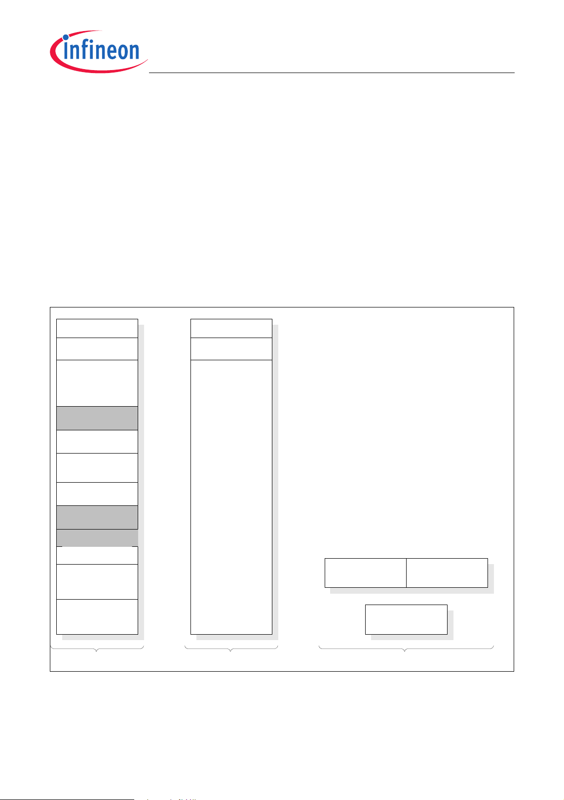
3.2 Memory Organization
The XC886/888 CPU operates in the following five address spaces:
• 12 Kbytes of Boot ROM program memory
• 256 bytes of internal RAM data memory
• 1.5 Kbytes of XRAM memory
(XRAM can be read/written as program memory or external data memory)
• A 128-byte Special Function Register area
• 24/32 Kbytes of Flash program memory (Flash devices); or
24/32 Kbytes of ROM program memory, with additional 4 Kbytes of Flash
(ROM devices)
Figure 7 illustrates the memory address spaces of the 32-Kbyte Flash devices. For the
24-Kbyte Flash devices, the shaded banks are not available.
XRAM
1.5 Kby tes
Boot ROM
12 Kby tes
D-Fl ash B ank 1
4 Kby tes
D-Fl ash B ank 0
4 Kby tes
D-Fl ash B ank 0
4 Kby tes
D-Fl ash B ank 1
4 Kby tes
P-Flas h Bank s 4 and 5
2 x 4 K bytes
P-Flas h Bank s 2 and 3
2 x 4 K bytes
P-Flas h Bank s 0 and 1
2 x 4 K bytes
1)
FFFF
F600
F000
C000
B000
A000
8000
7000
6000
5000
4000
2000
0000
H
H
H
H
H
H
H
H
H
H
H
H
H
XRAM
1.5 Kby tes
FFFF
F600
F000
0000
H
H
H
H
1)
Indirect
Addr ess
Internal RAM
7F
H
00
H
In 24-K byte Flash dev ic es, the upper 2Kby te of Bank s 4 and 5 ar e not avai labl e.
Direct
Addr ess
Special Function
Registers
Internal RA M
FF
H
80
H
Program Spac e Ex ternal Data Spac e Internal Data Spac e
Figure 7 Memory Map of XC886/888 Flash Device
For both 24-Kbyte and 32-Kbyte ROM devices, the last four bytes of the ROM from
7FFC
Data Sheet 20 V1.2, 2009-07
to 7FFFH are reserved for the ROM signature and cannot be used to store user
H
XC886/888CLM
Functional Description
code or data. Therefore, even though the ROM device contains either a 24-Kbyte or 32Kbyte ROM, the maximum size of code that can be placed in the ROM is the given size
less four bytes.
3.2.1 Memory Protection Strategy
The XC886/888 memory protection strategy includes:
• Read-out protection: The user is able to protect the contents in the Flash (for Flash
devices) and ROM (for ROM devices) memory from being read
– Flash protection is enabled by programming a valid password (8-bit non-zero
value) via BSL mode 6.
– ROM protection is fixed with the ROM mask and is always enabled.
• Flash program and erase protection: This feature is available only for Flash devices.
3.2.1.1 Flash Memory Protection
As long as a valid password is available, all external access to the device, including the
Flash, will be blocked.
For additional security, the Flash hardware protection can be enabled to implement a
second layer of read-out protection, as well as to enable program and erase protection.
Flash hardware protection is available only for Flash devices and comes in two modes:
• Mode 0: Only the P-Flash is protected; the D-Flash is unprotected
• Mode 1: Both the P-Flash and D-Flash are protected
The selection of each protection mode and the restrictions imposed are summarized in
Table 4.
Table 4 Flash Protection Modes
Flash Protection Without hardware
protection
Hardware
Protection Mode
Activation Program a valid password via BSL mode 6
Selection Bit 4 of password = 0 Bit 4 of password = 1
-01
With hardware protection
Bit 4 of password = 1
MSB of password = 0
MSB of password = 1
P-Flash
contents can be
read by
External access
to P-Flash
Data Sheet 21 V1.2, 2009-07
Read instructions in
any program memory
Not possible Not possible Not possible
Read instructions in
the P-Flash
Read instructions in
the P-Flash or DFlash

Table 4 Flash Protection Modes (cont’d)
XC886/888CLM
Functional Description
Flash Protection Without hardware
With hardware protection
protection
P-Flash program
Possible Not possible Not possible
and erase
D-Flash
contents can be
Read instructions in
any program memory
Read instructions in
any program memory
read by
External access
Not possible Not possible Not possible
to D-Flash
D-Flash
Possible Possible Not possible
program
D-Flash erase Possible Possible, on
condition that bit
DFLASHEN in
register MISC_CON
is set to 1 prior to
each erase operation
Read instructions in
the P-Flash or DFlash
Not possible
BSL mode 6, which is used for enabling Flash protection, can also be used for disabling
Flash protection. Here, the programmed password must be provided by the user. A
password match triggers an automatic erase of the protected P-Flash and D-Flash
contents, including the programmed password. The Flash protection is then disabled
upon the next reset.
For the ROM device, the ROM is protected at all times and BSL mode 6 is used only to
block external access to the device. However, unlike the Flash device, it is not possible
to disable the memory protection of the ROM device. Here, entering BSL mode 6 will
result in a protection error.
Note: If ROM read-out protection is enabled, only read instructions in the ROM memory
can target the ROM contents.
Although no protection scheme can be considered infallible, the XC886/888 memory
protection strategy provides a very high level of protection for a general purpose
microcontroller.
Data Sheet 22 V1.2, 2009-07

XC886/888CLM
Functional Description
3.2.2 Special Function Register
The Special Function Registers (SFRs) occupy direct internal data memory space in the
range 80
to FFH. All registers, except the program counter, reside in the SFR area. The
H
SFRs include pointers and registers that provide an interface between the CPU and the
on-chip peripherals. As the 128-SFR range is less than the total number of registers
required, address extension mechanisms are required to increase the number of
addressable SFRs. The address extension mechanisms include:
• Mapping
•Paging
3.2.2.1 Address Extension by Mapping
Address extension is performed at the system level by mapping. The SFR area is
extended into two portions: the standard (non-mapped) SFR area and the mapped SFR
area. Each portion supports the same address range 80
addressable SFRs to 256. The extended address range is not directly controlled by the
CPU instruction itself, but is derived from bit RMAP in the system control register
SYSCON0 at address 8F
. To access SFRs in the mapped area, bit RMAP in SFR
H
SYSCON0 must be set. Alternatively, the SFRs in the standard area can be accessed
by clearing bit RMAP. The SFR area can be selected as shown in Figure 8.
to FFH, bringing the number of
H
As long as bit RMAP is set, the mapped SFR area can be accessed. This bit is not
cleared automatically by hardware. Thus, before standard/mapped registers are
accessed, bit RMAP must be cleared/set, respectively, by software.
Data Sheet 23 V1.2, 2009-07

Functional Description
Standard Area (RMAP = 0)
Module 1 SFRs
XC886/888CLM
FF
H
SFR Data
(to/from CPU)
SYSCON0.RMAP
rw
Module 2 SFRs
…...
Module n SFRs
Mapped Area (RMAP = 1)
Module (n+1) SFRs
Module (n+2) SFRs
…...
80
FF
H
H
Module m SFRs
80
H
Direct
Internal Data
Memory Address
Figure 8 Address Extension by Mapping
Data Sheet 24 V1.2, 2009-07

XC886/888CLM
Functional Description
SYSCON0
System Control Register 0 Reset Value: 04
76543210
0 IMODE 0 1 0 RMAP
r rwrrrrw
Field Bits Type Description
RMAP 0rwInterrupt Node XINTR0 Enable
0 The access to the standard SFR area is
enabled
1 The access to the mapped SFR area is
enabled
H
1 2rReserved
Returns 1 if read; should be written with 1.
0 [7:5],
3,1
r Reserved
Returns 0 if read; should be written with 0.
Note: The RMAP bit should be cleared/set by ANL or ORL instructions.
3.2.2.2 Address Extension by Paging
Address extension is further performed at the module level by paging. With the address
extension by mapping, the XC886/888 has a 256-SFR address range. However, this is
still less than the total number of SFRs needed by the on-chip peripherals. To meet this
requirement, some peripherals have a built-in local address extension mechanism for
increasing the number of addressable SFRs. The extended address range is not directly
controlled by the CPU instruction itself, but is derived from bit field PAGE in the module
page register MOD_PAGE. Hence, the bit field PAGE must be programmed before
accessing the SFR of the target module. Each module may contain a different number
of pages and a different number of SFRs per page, depending on the specific
requirement. Besides setting the correct RMAP bit value to select the SFR area, the user
must also ensure that a valid PAGE is selected to target the desired SFR. A page inside
the extended address range can be selected as shown in Figure 9.
Data Sheet 25 V1.2, 2009-07

SFR Address
(from CPU)
XC886/888CLM
Functional Description
PAGE 0
SFR Data
(to/from CPU)
MOD_PAGE.PAGE
rw
SFR0
SFR1
…...
SFRx
PAGE 1
SFR0
SFR1
…...
SFRy
…...
PAGE q
SFR0
SFR1
…...
SFRz
Module
Figure 9 Address Extension by Paging
In order to access a register located in a page different from the actual one, the current
page must be exited. This is done by reprogramming the bit field PAGE in the page
register. Only then can the desired access be performed.
If an interrupt routine is initiated between the page register access and the module
register access, and the interrupt needs to access a register located in another page, the
current page setting can be saved, the new one programmed and the old page setting
restored. This is possible with the storage fields STx (x = 0 - 3) for the save and restore
action of the current page setting. By indicating which storage bit field should be used in
parallel with the new page value, a single write operation can:
• Save the contents of PAGE in STx before overwriting with the new value
(this is done in the beginning of the interrupt routine to save the current page setting
and program the new page number); or
Data Sheet 26 V1.2, 2009-07

XC886/888CLM
Functional Description
• Overwrite the contents of PAGE with the contents of STx, ignoring the value written
to the bit positions of PAGE
(this is done at the end of the interrupt routine to restore the previous page setting
before the interrupt occurred)
ST3
ST2
ST1
ST0
STNR
value update
PAGE
from CPU
Figure 10 Storage Elements for Paging
With this mechanism, a certain number of interrupt routines (or other routines) can
perform page changes without reading and storing the previously used page information.
The use of only write operations makes the system simpler and faster. Consequently,
this mechanism significantly improves the performance of short interrupt routines.
The XC886/888 supports local address extension for:
• Parallel Ports
• Analog-to-Digital Converter (ADC)
• Capture/Compare Unit 6 (CCU6)
• System Control Registers
Data Sheet 27 V1.2, 2009-07

XC886/888CLM
Functional Description
The page register has the following definition:
MOD_PAGE
Page Register for module MOD Reset Value: 00
76543210
OP STNR 0 PAGE
wwrrw
Field Bits Type Description
PAGE [2:0] rw Page Bits
When written, the value indicates the new page.
When read, the value indicates the currently active
page.
H
STNR [5:4] w Storage Number
This number indicates which storage bit field is the
target of the operation defined by bit field OP.
If OP = 10
,
B
the contents of PAGE are saved in STx before being
overwritten with the new value.
If OP = 11
,
B
the contents of PAGE are overwritten by the
contents of STx. The value written to the bit positions
of PAGE is ignored.
00 ST0 is selected.
01 ST1 is selected.
10 ST2 is selected.
11 ST3 is selected.
Data Sheet 28 V1.2, 2009-07

Field Bits Type Description
OP [7:6] w Operation
0X Manual page mode. The value of STNR is
ignored and PAGE is directly written.
10 New page programming with automatic page
saving. The value written to the bit positions of
PAGE is stored. In parallel, the previous
contents of PAGE are saved in the storage bit
field STx indicated by STNR.
11 Automatic restore page action. The value
written to the bit positions PAGE is ignored
and instead, PAGE is overwritten by the
contents of the storage bit field STx indicated
by STNR.
XC886/888CLM
Functional Description
0 3rReserved
Returns 0 if read; should be written with 0.
3.2.3 Bit Protection Scheme
The bit protection scheme prevents direct software writing of selected bits (i.e., protected
bits) using the PASSWD register. When the bit field MODE is 11
bit field PASS opens access to writing of all protected bits, and writing 10101
field PASS closes access to writing of all protected bits. In both cases, the value of the
bit field MODE is not changed even if PASSWD register is written with 98
only be changed when bit field PASS is written with 11000
, for example, writing D0H to
B
PASSWD register disables the bit protection scheme.
Note that access is opened for maximum 32 CCLKs if the “close access” password is not
written. If “open access” password is written again before the end of 32 CCLK cycles,
there will be a recount of 32 CCLK cycles. The protected bits include the N- and KDivider bits, NDIV and KDIV; the Watchdog Timer enable bit, WDTEN; and the powerdown and slow-down enable bits, PD and SD.
, writing 10011B to the
B
to the bit
B
or A8H. It can
H
Data Sheet 29 V1.2, 2009-07

XC886/888CLM
Functional Description
3.2.3.1 Password Register
PASSWD
Password Register Reset Value: 07
76543210
H
PASS
wh rh rw
PROTECT
_S
Field Bits Type Description
MODE [1:0] rw Bit Protection Scheme Control Bits
00 Scheme disabled - direct access to the
protected bits is allowed.
11 Scheme enabled - the bit field PASS has to be
written with the passwords to open and close
the access to protected bits. (default)
Others:Scheme Enabled.
These two bits cannot be written directly. To change
the value between 11
must be written with 11000
and 00B, the bit field PASS
B
; only then, will the
B
MODE[1:0] be registered.
PROTECT_S 2rhBit Protection Signal Status Bit
This bit shows the status of the protection.
0 Software is able to write to all protected bits.
1 Software is unable to write to any protected
bits.
MODE
PASS [7:3] wh Password Bits
The Bit Protection Scheme only recognizes three
patterns.
11000B Enables writing of the bit field MODE.
10011
10101
Data Sheet 30 V1.2, 2009-07
Opens access to writing of all protected bits.
B
Closes access to writing of all protected bits
B

XC886/888CLM
Functional Description
3.2.4 XC886/888 Register Overview
The SFRs of the XC886/888 are organized into groups according to their functional units.
The contents (bits) of the SFRs are summarized in Chapter 3.2.4.1 to Chapter 3.2.4.14.
Note: The addresses of the bitaddressable SFRs appear in bold typeface.
3.2.4.1 CPU Registers
The CPU SFRs can be accessed in both the standard and mapped memory areas
(RMAP = 0 or 1).
Table 5 CPU Register Overview
Addr Register Name Bit 7 6 5 4 3 2 1 0
RMAP = 0 or 1
81
82
83
87
88
89
8A
8B
8C
8D
98
99
A2
SP Reset: 07
H
Stack Pointer Register
DPL Reset: 00
H
Data Pointer Register Low
DPH Reset: 00
H
Data Pointer Register High
PCON Reset: 00
H
Power Control Register
TCON Reset: 00
H
Timer Control Register
TMOD Reset: 00
H
Timer Mode Register
TL0 Reset: 00
H
Timer 0 Register Low
TL1 Reset: 00
H
Timer 1 Register Low
TH0 Reset: 00
H
Timer 0 Register High
TH1 Reset: 00
H
Timer 1 Register High
SCON Reset: 00
H
Serial Channel Control Register
SBUF Reset: 00
H
Serial Data Buffer Register
EO Reset: 00
H
Extended Operation Register
Bit Field
H
Type rw
Bit Field
H
Type rw rw rw rw rw rw rw rw
Bit Field
H
Type rw rw rw rw rw rw rw rw
Bit Field
H
Type rw r rw rw r rw
Bit Field
H
Type rwh rw rwh rw rwh rw rwh rw
Bit Field
H
Type rw rw rw rw rw rw
Bit Field
H
Type rwh
Bit Field
H
Type rwh
Bit Field
H
Type rwh
Bit Field
H
Type rwh
Bit Field
H
Type rw rw rw rw rw rwh rwh rwh
Bit Field
H
Type rwh
Bit Field
H
Type r rw r rw
DPL7 DPL6 DPL5 DPL4 DPL3 DPL2 DPL1 DPL0
DPH7 DPH6 DPH5 DPH4 DPH3 DPH2 DPH1 DPH0
SMOD 0 GF1 GF0 0 IDLE
TF1 TR1 TF0 TR0 IE1 IT1 IE0 IT0
GATE1T1S T1M GATE0T0S T0M
SM0 SM1 SM2 REN TB8 RB8 TI RI
0 TRAP_
SP
VAL
VAL
VAL
VAL
VAL
0 DPSE
EN
L0
Data Sheet 31 V1.2, 2009-07

XC886/888CLM
Functional Description
Table 5 CPU Register Overview (cont’d)
Addr Register Name Bit 7 6 5 4 3 2 1 0
A8
B8
B9
D0
E0
E8
F0
F8
F9
IEN0 Reset: 00
H
Interrupt Enable Register 0
IP Reset: 00
H
Interrupt Priority Register
IPH Reset: 00
H
Interrupt Priority High Register
PSW Reset: 00
H
Program Status Word Register
ACC Reset: 00
H
Accumulator Register
IEN1 Reset: 00
H
Interrupt Enable Register 1
B Reset: 00
H
B Register
IP1 Reset: 00
H
Interrupt Priority 1 Register
IPH1 Reset: 00
H
Interrupt Priority 1 High Register
Bit Field
H
Type rw r rwrwrwrwrwrw
Bit Field
H
Type r rwrwrwrwrwrw
Bit Field
H
Type r rwrwrwrwrwrw
Bit Field
H
Type rwh rwh rw rw rw rwh rw rh
Bit Field
H
Type rw rw rw rw rw rw rw rw
Bit Field
H
Type rw rw rw rw rw rw rw rw
Bit Field
H
Type rw rw rw rw rw rw rw rw
Bit Field
H
Type rw rw rw rw rw rw rw rw
Bit Field
H
Type rw rw rw rw rw rw rw rw
EA 0 ET2 ES ET1 EX1 ET0 EX0
0 PT2 PS PT1 PX1 PT0 PX0
0 PT2H PSH PT1H PX1H PT0H PX0H
CY AC F0 RS1 RS0 OV F1 P
ACC7 ACC6 ACC5 ACC4 ACC3 ACC2 ACC1 ACC0
ECCIP3ECCIP2ECCIP1ECCIP0EXM EX2 ESSC EADC
B7 B6 B5 B4 B3 B2 B1 B0
PCCIP3PCCIP2PCCIP1PCCIP0PXM PX2 PSSC PADC
PCCIP3HPCCIP2HPCCIP1HPCCIP0HPXMH PX2H PSSCHPADC
H
3.2.4.2 MDU Registers
The MDU SFRs can be accessed in the mapped memory area (RMAP = 1).
Table 6 MDU Register Overview
Addr Register Name Bit 7 6 5 4 3 2 1 0
RMAP = 1
B0
B1
B2
B2
B3
MDUSTAT Reset: 00
H
MDU Status Register
MDUCON Reset: 00
H
MDU Control Register
MD0 Reset: 00
H
MDU Operand Register 0
MR0 Reset: 00
H
MDU Result Register 0
MD1 Reset: 00
H
MDU Operand Register 1
Bit Field
H
Type r rh rwh rwh
Bit Field
H
Type rw rw rw rwh rw
Bit Field
H
Type rw
Bit Field
H
Type rh
Bit Field
H
Type rw
IE IR RSEL STAR
0 BSY IERR IRDY
OPCODE
T
DATA
DATA
DATA
Data Sheet 32 V1.2, 2009-07

XC886/888CLM
Functional Description
Table 6 MDU Register Overview (cont’d)
Addr Register Name Bit 7 6 5 4 3 2 1 0
B3
B4
B4
B5
B5
B6
B6
B7
B7
MR1 Reset: 00
H
MDU Result Register 1
MD2 Reset: 00
H
MDU Operand Register 2
MR2 Reset: 00
H
MDU Result Register 2
MD3 Reset: 00
H
MDU Operand Register 3
MR3 Reset: 00
H
MDU Result Register 3
MD4 Reset: 00
H
MDU Operand Register 4
MR4 Reset: 00
H
MDU Result Register 4
MD5 Reset: 00
H
MDU Operand Register 5
MR5 Reset: 00
H
MDU Result Register 5
Bit Field
H
Type rh
Bit Field
H
Type rw
Bit Field
H
Type rh
Bit Field
H
Type rw
Bit Field
H
Type rh
Bit Field
H
Type rw
Bit Field
H
Type rh
Bit Field
H
Type rw
Bit Field
H
Type rh
DATA
DATA
DATA
DATA
DATA
DATA
DATA
DATA
DATA
3.2.4.3 CORDIC Registers
The CORDIC SFRs can be accessed in the mapped memory area (RMAP = 1).
Table 7 CORDIC Register Overview
Addr Register Name Bit 7 6 5 4 3 2 1 0
RMAP = 1
9A
9B
9C
9D
9E
9F
CD_CORDXL Reset: 00
H
CORDIC X Data Low Byte
CD_CORDXH Reset: 00
H
CORDIC X Data High Byte
CD_CORDYL Reset: 00
H
CORDIC Y Data Low Byte
CD_CORDYH Reset: 00
H
CORDIC Y Data High Byte
CD_CORDZL Reset: 00
H
CORDIC Z Data Low Byte
CD_CORDZH Reset: 00
H
CORDIC Z Data High Byte
Bit Field
H
Type rw
Bit Field
H
Type rw
Bit Field
H
Type rw
Bit Field
H
Type rw
Bit Field
H
Type rw
Bit Field
H
Type rw
DATAL
DATAH
DATAL
DATAH
DATAL
DATAH
Data Sheet 33 V1.2, 2009-07

XC886/888CLM
Functional Description
Table 7 CORDIC Register Overview (cont’d)
Addr Register Name Bit 7 6 5 4 3 2 1 0
A0
A1
CD_STATC Reset: 00
H
CORDIC Status and Data
Control Register
CD_CON Reset: 00
H
CORDIC Control Register
Bit Field
H
Type rw rw rw rw rw rwh rh rh
Bit Field
H
Type rw rw rw rw rw rwh
KEEPZKEEPYKEEPXDMAP INT_ENEOC ERRORBSY
MPS X_USIGNST_M
ODE
ROTV
EC
MODE ST
3.2.4.4 System Control Registers
The system control SFRs can be accessed in the mapped memory area (RMAP = 0).
Table 8 SCU Register Overview
Addr Register Name Bit 7 6 5 4 3 2 1 0
RMAP = 0 or 1
8F
RMAP = 0
BF
RMAP = 0, PAGE 0
B3
B4
B5
B6
B7
BA
BB
SYSCON0 Reset: 04
H
System Control Register 0
SCU_PAGE Reset: 00
H
Page Register
MODPISEL Reset: 00
H
Peripheral Input Select Register
IRCON0 Reset: 00
H
Interrupt Request Register 0
IRCON1 Reset: 00
H
Interrupt Request Register 1
IRCON2 Reset: 00
H
Interrupt Request Register 2
EXICON0 Reset: F0
H
External Interrupt Control
Register 0
EXICON1 Reset: 3F
H
External Interrupt Control
Register 1
NMICON Reset: 00
H
NMI Control Register
Bit Field
H
Type r rw r r r rw
Bit Field
H
Type w w r rw
Bit Field
H
Type r rwrwrwrwrwrwrw
Bit Field
H
Type r rwh rwh rwh rwh rwh rwh rwh
Bit Field
H
Type r rwh rwh rwh rwh rwh rwh rwh
Bit Field
H
Type rrwhrrwh
Bit Field
H
Type rw rw rw rw
Bit Field
H
Typer rwrwrw
Bit Field
H
Type r rwrwrwrwrwrwrw
0 URRISHJTAGT
0 EXINT6EXINT5EXINT4EXINT3EXINT2EXINT1EXINT
0 CANS
0 NMI
0 IMOD
OP STNR 0 PAGE
DIS
RC2
EXINT3 EXINT2 EXINT1 EXINT0
0 EXINT6 EXINT5 EXINT4
ECC
CANS
RC1
0 CANS
NMI
VDDP
E
JTAGT
CKS
ADCSR1ADCSR0RIR TIR EIR
RC3
NMI
VDD
0 1 0 RMAP
EXINT
NMI
OCDS
2IS
EXINT
FLASH
EXINT
1IS
0 CANS
NMI
0IS
NMI
PLL
URRIS
0
RC0
NMI
WDT
Data Sheet 34 V1.2, 2009-07

XC886/888CLM
Functional Description
Table 8 SCU Register Overview (cont’d)
Addr Register Name Bit 7 6 5 4 3 2 1 0
BC
BD
BE
E9
EA
EB
RMAP = 0, PAGE 1
B3
B4
B5
B6
B7
BA
BB
BC
BD
NMISR Reset: 00
H
NMI Status Register
BCON Reset: 00
H
Baud Rate Control Register
BG Reset: 00
H
Baud Rate Timer/Reload
Register
FDCON Reset: 00
H
Fractional Divider Control
Register
FDSTEP Reset: 00
H
Fractional Divider Reload
Register
FDRES Reset: 00
H
Fractional Divider Result
Register
ID Reset: UU
H
Identity Register
PMCON0 Reset: 00
H
Power Mode Control Register 0
PMCON1 Reset: 00
H
Power Mode Control Register 1
OSC_CON Reset: 08
H
OSC Control Register
PLL_CON Reset: 90
H
PLL Control Register
CMCON Reset: 10
H
Clock Control Register
PASSWD Reset: 07
H
Password Register
FEAL Reset: 00
H
Flash Error Address Register
Low
FEAH Reset: 00
H
Flash Error Address Register
High
Bit Field
H
Type r rwh rwh rwh rwh rwh rwh rwh
Bit Field
H
Type rw r rw rw rw
Bit Field
H
Type rwh
Bit Field
H
Type rw rw rwh rwh rwh rwh rw rw
Bit Field
H
Type rw
Bit Field
H
Type rh
Bit Field
H
Type r r
Bit Field
H
Type r rwh rwh rw rw rwh rw
Bit Field
H
Type r rwrwrwrwrwrwrw
Bit Field
H
Type r rw rw rw rwh rh
Bit Field
H
Type rw rw rw rwh rh
Bit Field
H
Type rw rw r rw rw
Bit Field
H
Type wh rh rw
Bit Field
H
Type rh
Bit Field
H
Type rh
0 FNMI
ECC
BGSEL 0 BRDIS BRPRE R
BGS SYNENERRSYNEOFSYNBRK NDOV FDM FDEN
0 WDT
RST
0 CDC_
VCO
SEL
DIS
KDIV 0 FCCF
FNMI
VDDP
PRODID VERID
WKRS WK
CAN_
DIS
0 OSCPDXPD OSCSSORD
NDIV VCO
PASS PROT
FNMI
VDD
SEL
MDU_
DIS
ECCERRADDR
ECCERRADDR
FNMI
OCDS
BR_VALUE
STEP
RESULT
SD PD WS
T2_
DIS
BYP
G
FNMI
FLASH
CCU_
DIS
OSC
DISC
CLKREL
ECT_S
FNMI
PLL
SSC_
DIS
RES
RESLDLOCK
MODE
FNMI
WDT
ADC_
DIS
OSCR
Data Sheet 35 V1.2, 2009-07

XC886/888CLM
Functional Description
Table 8 SCU Register Overview (cont’d)
Addr Register Name Bit 7 6 5 4 3 2 1 0
BE
E9
RMAP = 0, PAGE 3
B3
B4
B5
B7
BA
BB
BD
COCON Reset: 00
H
Clock Output Control Register
MISC_CON Reset: 00
H
Miscellaneous Control Register
XADDRH Reset: F0
H
On-chip XRAM Address Higher
Order
IRCON3 Reset: 00
H
Interrupt Request Register 3
IRCON4 Reset: 00
H
Interrupt Request Register 4
MODPISEL1 Reset: 00
H
Peripheral Input Select Register
1
MODPISEL2 Reset: 00
H
Peripheral Input Select Register
2
PMCON2 Reset: 00
H
Power Mode Control Register 2
MODSUSP Reset: 01
H
Module Suspend Control
Register
Bit Field
H
Type r rw rw rw
Bit Field
H
Type r rwh
Bit Field
H
Type rw
Bit Field
H
Type r rwh rwh r rwh rwh
Bit Field
H
Type r rwh rwh r rwh rwh
Bit Field
H
Type rw r rw rw rw rw
Bit Field
H
Type r rw rw rw rw
Bit Field
H
Type r rw rw
Bit Field
H
Type r rw rw rw rw rw
0 TLEN COUT
0 CANS
0 CANS
EXINT
6IS
0 UR1RIS T21EXISJTAGT
0 T21IS T2IS T1IS T0IS
0 T21SUSPT2SUSPT13SUSPT12SUSPWDTS
S
0 DFLAS
ADDRH
RC5
RC7
CCU6
SR1
CCU6
SR3
0 UART
0 CANS
0 CANS
COREL
RC4
RC6
DIS1
1_DIS
HEN
CCU6
SR0
CCU6
SR2
JTAGT
CKS1
T21_D
USP
IS
3.2.4.5 WDT Registers
The WDT SFRs can be accessed in the mapped memory area (RMAP = 1).
Table 9 WDT Register Overview
Addr Register Name Bit 7 6 5 4 3 2 1 0
RMAP = 1
BB
BC
BD
WDTCON Reset: 00
H
Watchdog Timer Control
Register
WDTREL Reset: 00
H
Watchdog Timer Reload
Register
WDTWINB Reset: 00
H
Watchdog Window-Boundary
Count Register
Bit Field
H
Type r rw rh r rw rwh rw
Bit Field
H
Type rw
Bit Field
H
Type rw
Data Sheet 36 V1.2, 2009-07
0 WINBENWDTP
R
WDTREL
WDTWINB
0 WDTENWDTRSWDTI
N

XC886/888CLM
Functional Description
Table 9 WDT Register Overview (cont’d)
Addr Register Name Bit 7 6 5 4 3 2 1 0
BE
BF
WDTL Reset: 00
H
Watchdog Timer Register Low
WDTH Reset: 00
H
Watchdog Timer Register High
Bit Field
H
Type rh
Bit Field
H
Type rh
WDT
WDT
3.2.4.6 Port Registers
The Port SFRs can be accessed in the standard memory area (RMAP = 0).
Table 10 Port Register Overview
Addr Register Name Bit 7 6 5 4 3 2 1 0
RMAP = 0
B2
RMAP = 0, PAGE 0
80
86
90
91
92
93
A0
A1
B0
B1
C8
C9
PORT_PAGE Reset: 00
H
Page Register
P0_DATA Reset: 00
H
P0 Data Register
P0_DIR Reset: 00
H
P0 Direction Register
P1_DATA Reset: 00
H
P1 Data Register
P1_DIR Reset: 00
H
P1 Direction Register
P5_DATA Reset: 00
H
P5 Data Register
P5_DIR Reset: 00
H
P5 Direction Register
P2_DATA Reset: 00
H
P2 Data Register
P2_DIR Reset: 00
H
P2 Direction Register
P3_DATA Reset: 00
H
P3 Data Register
P3_DIR Reset: 00
H
P3 Direction Register
P4_DATA Reset: 00
H
P4 Data Register
P4_DIR Reset: 00
H
P4 Direction Register
Bit Field
H
Type w w r rw
Bit Field
H
Type rw rw rw rw rw rw rw rw
Bit Field
H
Type rw rw rw rw rw rw rw rw
Bit Field
H
Type rw rw rw rw rw rw rw rw
Bit Field
H
Type rw rw rw rw rw rw rw rw
Bit Field
H
Type rw rw rw rw rw rw rw rw
Bit Field
H
Type rw rw rw rw rw rw rw rw
Bit Field
H
Type rw rw rw rw rw rw rw rw
Bit Field
H
Type rw rw rw rw rw rw rw rw
Bit Field
H
Type rw rw rw rw rw rw rw rw
Bit Field
H
Type rw rw rw rw rw rw rw rw
Bit Field
H
Type rw rw rw rw rw rw rw rw
Bit Field
H
Type rw rw rw rw rw rw rw rw
OP STNR 0 PAGE
P7 P6 P5 P4 P3 P2 P1 P0
P7 P6 P5 P4 P3 P2 P1 P0
P7 P6 P5 P4 P3 P2 P1 P0
P7 P6 P5 P4 P3 P2 P1 P0
P7 P6 P5 P4 P3 P2 P1 P0
P7 P6 P5 P4 P3 P2 P1 P0
P7 P6 P5 P4 P3 P2 P1 P0
P7 P6 P5 P4 P3 P2 P1 P0
P7 P6 P5 P4 P3 P2 P1 P0
P7 P6 P5 P4 P3 P2 P1 P0
P7 P6 P5 P4 P3 P2 P1 P0
P7 P6 P5 P4 P3 P2 P1 P0
Data Sheet 37 V1.2, 2009-07

XC886/888CLM
Functional Description
Table 10 Port Register Overview (cont’d)
Addr Register Name Bit 7 6 5 4 3 2 1 0
RMAP = 0, PAGE 1
80
86
90
91
92
93
A0
A1
B0
B1
C8
C9
RMAP = 0, PAGE 2
80
86
90
91
92
P0_PUDSEL Reset: FF
H
P0 Pull-Up/Pull-Down Select
Register
P0_PUDEN Reset: C4
H
P0 Pull-Up/Pull-Down Enable
Register
P1_PUDSEL Reset: FF
H
P1 Pull-Up/Pull-Down Select
Register
P1_PUDEN Reset: FF
H
P1 Pull-Up/Pull-Down Enable
Register
P5_PUDSEL Reset: FF
H
P5 Pull-Up/Pull-Down Select
Register
P5_PUDEN Reset: FF
H
P5 Pull-Up/Pull-Down Enable
Register
P2_PUDSEL Reset: FF
H
P2 Pull-Up/Pull-Down Select
Register
P2_PUDEN Reset: 00
H
P2 Pull-Up/Pull-Down Enable
Register
P3_PUDSEL Reset: BF
H
P3 Pull-Up/Pull-Down Select
Register
P3_PUDEN Reset: 40
H
P3 Pull-Up/Pull-Down Enable
Register
P4_PUDSEL Reset: FF
H
P4 Pull-Up/Pull-Down Select
Register
P4_PUDEN Reset: 04
H
P4 Pull-Up/Pull-Down Enable
Register
P0_ALTSEL0 Reset: 00
H
P0 Alternate Select 0 Register
P0_ALTSEL1 Reset: 00
H
P0 Alternate Select 1 Register
P1_ALTSEL0 Reset: 00
H
P1 Alternate Select 0 Register
P1_ALTSEL1 Reset: 00
H
P1 Alternate Select 1 Register
P5_ALTSEL0 Reset: 00
H
P5 Alternate Select 0 Register
Bit Field
H
Type rw rw rw rw rw rw rw rw
Bit Field
H
Type rw rw rw rw rw rw rw rw
Bit Field
H
Type rw rw rw rw rw rw rw rw
Bit Field
H
Type rw rw rw rw rw rw rw rw
Bit Field
H
Type rw rw rw rw rw rw rw rw
Bit Field
H
Type rw rw rw rw rw rw rw rw
Bit Field
H
Type rw rw rw rw rw rw rw rw
Bit Field
H
Type rw rw rw rw rw rw rw rw
Bit Field
H
Type rw rw rw rw rw rw rw rw
Bit Field
H
Type rw rw rw rw rw rw rw rw
Bit Field
H
Type rw rw rw rw rw rw rw rw
Bit Field
H
Type rw rw rw rw rw rw rw rw
Bit Field
H
Type rw rw rw rw rw rw rw rw
Bit Field
H
Type rw rw rw rw rw rw rw rw
Bit Field
H
Type rw rw rw rw rw rw rw rw
Bit Field
H
Type rw rw rw rw rw rw rw rw
Bit Field
H
Type rw rw rw rw rw rw rw rw
P7 P6 P5 P4 P3 P2 P1 P0
P7 P6 P5 P4 P3 P2 P1 P0
P7 P6 P5 P4 P3 P2 P1 P0
P7 P6 P5 P4 P3 P2 P1 P0
P7 P6 P5 P4 P3 P2 P1 P0
P7 P6 P5 P4 P3 P2 P1 P0
P7 P6 P5 P4 P3 P2 P1 P0
P7 P6 P5 P4 P3 P2 P1 P0
P7 P6 P5 P4 P3 P2 P1 P0
P7 P6 P5 P4 P3 P2 P1 P0
P7 P6 P5 P4 P3 P2 P1 P0
P7 P6 P5 P4 P3 P2 P1 P0
P7 P6 P5 P4 P3 P2 P1 P0
P7 P6 P5 P4 P3 P2 P1 P0
P7 P6 P5 P4 P3 P2 P1 P0
P7 P6 P5 P4 P3 P2 P1 P0
P7 P6 P5 P4 P3 P2 P1 P0
Data Sheet 38 V1.2, 2009-07

XC886/888CLM
Functional Description
Table 10 Port Register Overview (cont’d)
Addr Register Name Bit 7 6 5 4 3 2 1 0
93
B0
B1
C8
C9
RMAP = 0, PAGE 3
80
90
92
B0
C8
P5_ALTSEL1 Reset: 00
H
P5 Alternate Select 1 Register
P3_ALTSEL0 Reset: 00
H
P3 Alternate Select 0 Register
P3_ALTSEL1 Reset: 00
H
P3 Alternate Select 1 Register
P4_ALTSEL0 Reset: 00
H
P4 Alternate Select 0 Register
P4_ALTSEL1 Reset: 00
H
P4 Alternate Select 1 Register
P0_OD Reset: 00
H
P0 Open Drain Control Register
P1_OD Reset: 00
H
P1 Open Drain Control Register
P5_OD Reset: 00
H
P5 Open Drain Control Register
P3_OD Reset: 00
H
P3 Open Drain Control Register
P4_OD Reset: 00
H
P4 Open Drain Control Register
Bit Field
H
Type rw rw rw rw rw rw rw rw
Bit Field
H
Type rw rw rw rw rw rw rw rw
Bit Field
H
Type rw rw rw rw rw rw rw rw
Bit Field
H
Type rw rw rw rw rw rw rw rw
Bit Field
H
Type rw rw rw rw rw rw rw rw
Bit Field
H
Type rw rw rw rw rw rw rw rw
Bit Field
H
Type rw rw rw rw rw rw rw rw
Bit Field
H
Type rw rw rw rw rw rw rw rw
Bit Field
H
Type rw rw rw rw rw rw rw rw
Bit Field
H
Type rw rw rw rw rw rw rw rw
P7 P6 P5 P4 P3 P2 P1 P0
P7 P6 P5 P4 P3 P2 P1 P0
P7 P6 P5 P4 P3 P2 P1 P0
P7 P6 P5 P4 P3 P2 P1 P0
P7 P6 P5 P4 P3 P2 P1 P0
P7 P6 P5 P4 P3 P2 P1 P0
P7 P6 P5 P4 P3 P2 P1 P0
P7 P6 P5 P4 P3 P2 P1 P0
P7 P6 P5 P4 P3 P2 P1 P0
P7 P6 P5 P4 P3 P2 P1 P0
3.2.4.7 ADC Registers
The ADC SFRs can be accessed in the standard memory area (RMAP = 0).
Table 11 ADC Register Overview
AddrRegister Name Bit 76543210
RMAP = 0
D1
RMAP = 0, PAGE 0
CA
CB
CC
ADC_PAGE Reset: 00
H
Page Register
ADC_GLOBCTR Reset: 30
H
Global Control Register
ADC_GLOBSTR Reset: 00
H
Global Status Register
ADC_PRAR Reset: 00
H
Priority and Arbitration Register
Data Sheet 39 V1.2, 2009-07
Bit Field
H
Type w w r rw
Bit Field
H
Type rw rw rw r
Bit Field
H
Type r rh r rh rh
Bit Field
H
Type rw rw r rw rw rw rw rw
OP STNR 0 PAGE
ANON DW CTC 0
0 CHNR 0 SAMPLEBUSY
ASEN1ASEN
0
0 ARBM CSM1 PRIO1 CSM0 PRIO0

XC886/888CLM
Functional Description
Table 11 ADC Register Overview (cont’d)
AddrRegister Name Bit 76543210
CD
CE
CF
RMAP = 0, PAGE 1
CA
CB
CC
CD
CE
CF
D2
D3
RMAP = 0, PAGE 2
CA
CB
CC
CD
CE
CF
D2
ADC_LCBR Reset: B7
H
Limit Check Boundary Register
ADC_INPCR0 Reset: 00
H
Input Class 0 Register
ADC_ETRCR Reset: 00
H
External Trigger Control
Register
ADC_CHCTR0 Reset: 00
H
Channel Control Register 0
ADC_CHCTR1 Reset: 00
H
Channel Control Register 1
ADC_CHCTR2 Reset: 00
H
Channel Control Register 2
ADC_CHCTR3 Reset: 00
H
Channel Control Register 3
ADC_CHCTR4 Reset: 00
H
Channel Control Register 4
ADC_CHCTR5 Reset: 00
H
Channel Control Register 5
ADC_CHCTR6 Reset: 00
H
Channel Control Register 6
ADC_CHCTR7 Reset: 00
H
Channel Control Register 7
ADC_RESR0L Reset: 00
H
Result Register 0 Low
ADC_RESR0H Reset: 00
H
Result Register 0 High
ADC_RESR1L Reset: 00
H
Result Register 1 Low
ADC_RESR1H Reset: 00
H
Result Register 1 High
ADC_RESR2L Reset: 00
H
Result Register 2 Low
ADC_RESR2H Reset: 00
H
Result Register 2 High
ADC_RESR3L Reset: 00
H
Result Register 3 Low
Bit Field
H
Type rw rw
Bit Field
H
Type rw
Bit Field
H
Type rw rw rw rw
Bit Field
H
Type r rw r rw
Bit Field
H
Type r rw r rw
Bit Field
H
Type r rw r rw
Bit Field
H
Type r rw r rw
Bit Field
H
Type r rw r rw
Bit Field
H
Type r rw r rw
Bit Field
H
Type r rw r rw
Bit Field
H
Type r rw r rw
Bit Field
H
Type rh r rh rh rh
Bit Field
H
Type rh
Bit Field
H
Type rh r rh rh rh
Bit Field
H
Type rh
Bit Field
H
Type rh r rh rh rh
Bit Field
H
Type rh
Bit Field
H
Type rh r rh rh rh
SYNEN1SYNE
0 LCC 0 RESRSEL
0 LCC 0 RESRSEL
0 LCC 0 RESRSEL
0 LCC 0 RESRSEL
0 LCC 0 RESRSEL
0 LCC 0 RESRSEL
0 LCC 0 RESRSEL
0 LCC 0 RESRSEL
RESULT 0 VF DRC CHNR
RESULT 0 VF DRC CHNR
RESULT 0 VF DRC CHNR
RESULT 0 VF DRC CHNR
BOUND1 BOUND0
STC
ETRSEL1 ETRSEL0
N0
RESULT
RESULT
RESULT
Data Sheet 40 V1.2, 2009-07

XC886/888CLM
Functional Description
Table 11 ADC Register Overview (cont’d)
AddrRegister Name Bit 76543210
D3
RMAP = 0, PAGE 3
CA
CB
CC
CD
CE
CF
D2
D3
RMAP = 0, PAGE 4
CA
CB
CC
CD
CE
RMAP = 0, PAGE 5
CA
CB
ADC_RESR3H Reset: 00
H
Result Register 3 High
ADC_RESRA0L Reset: 00
H
Result Register 0, View A Low
ADC_RESRA0H Reset: 00
H
Result Register 0, View A High
ADC_RESRA1L Reset: 00
H
Result Register 1, View A Low
ADC_RESRA1H Reset: 00
H
Result Register 1, View A High
ADC_RESRA2L Reset: 00
H
Result Register 2, View A Low
ADC_RESRA2H Reset: 00
H
Result Register 2, View A High
ADC_RESRA3L Reset: 00
H
Result Register 3, View A Low
ADC_RESRA3H Reset: 00
H
Result Register 3, View A High
ADC_RCR0 Reset: 00
H
Result Control Register 0
ADC_RCR1 Reset: 00
H
Result Control Register 1
ADC_RCR2 Reset: 00
H
Result Control Register 2
ADC_RCR3 Reset: 00
H
Result Control Register 3
ADC_VFCR Reset: 00
H
Valid Flag Clear Register
ADC_CHINFR Reset: 00
H
Channel Interrupt Flag Register
ADC_CHINCR Reset: 00
H
Channel Interrupt Clear Register
Bit Field
H
Type rh
Bit Field
H
Type rh rh rh rh
Bit Field
H
Type rh
Bit Field
H
Type rh rh rh rh
Bit Field
H
Type rh
Bit Field
H
Type rh rh rh rh
Bit Field
H
Type rh
Bit Field
H
Type rh rh rh rh
Bit Field
H
Type rh
Bit Field
H
Type rw rw r rw r rw
Bit Field
H
Type rw rw r rw r rw
Bit Field
H
Type rw rw r rw r rw
Bit Field
H
Type rw rw r rw r rw
Bit Field
H
Type r w w w w
Bit Field
H
Type rh rh rh rh rh rh rh rh
Bit Field
H
Typewwwwwwww
CHINF7CHINF6CHINF5CHINF4CHINF3CHINF2CHINF1CHINF
CHINC7CHINC6CHINC5CHINC4CHINC3CHINC2CHINC1CHINC
RESULT VF DRC CHNR
RESULT VF DRC CHNR
RESULT VF DRC CHNR
RESULT VF DRC CHNR
VFCTRWFR 0 IEN 0 DRCT
VFCTRWFR 0 IEN 0 DRCT
VFCTRWFR 0 IEN 0 DRCT
VFCTRWFR 0 IEN 0 DRCT
0 VFC3 VFC2 VFC1 VFC0
RESULT
RESULT
RESULT
RESULT
RESULT
R
R
R
R
0
0
Data Sheet 41 V1.2, 2009-07

XC886/888CLM
Functional Description
Table 11 ADC Register Overview (cont’d)
AddrRegister Name Bit 76543210
CC
CD
CE
CF
D2
D3
RMAP = 0, PAGE 6
CA
CB
CC
CD
CE
CF
D2
D2
ADC_CHINSR Reset: 00
H
Channel Interrupt Set Register
ADC_CHINPR Reset: 00
H
Channel Interrupt Node Pointer
Register
ADC_EVINFR Reset: 00
H
Event Interrupt Flag Register
ADC_EVINCR Reset: 00
H
Event Interrupt Clear Flag
Register
ADC_EVINSR Reset: 00
H
Event Interrupt Set Flag Register
ADC_EVINPR Reset: 00
H
Event Interrupt Node Pointer
Register
ADC_CRCR1 Reset: 00
H
Conversion Request Control
Register 1
ADC_CRPR1 Reset: 00
H
Conversion Request Pending
Register 1
ADC_CRMR1 Reset: 00
H
Conversion Request Mode
Register 1
ADC_QMR0 Reset: 00
H
Queue Mode Register 0
ADC_QSR0 Reset: 20
H
Queue Status Register 0
ADC_Q0R0 Reset: 00
H
Queue 0 Register 0
ADC_QBUR0 Reset: 00
H
Queue Backup Register 0
ADC_QINR0 Reset: 00
H
Queue Input Register 0
Bit Field
H
Typewwwwwwww
Bit Field
H
Type rw rw rw rw rw rw rw rw
Bit Field
H
Type rh rh rh rh r rh rh
Bit Field
H
Typewwww r ww
Bit Field
H
Typewwww r ww
Bit Field
H
Type rw rw rw rw r rw rw
Bit Field
H
Type rwh rwh rwh rwh r
Bit Field
H
Type rwh rwh rwh rwh r
Bit Field
H
Type r w w rw rw rw r rw
Bit Field
H
Typewwww rrwrrw
Bit Field
H
Type r r rh rh r rh
Bit Field
H
Type rh rh rh rh r rh
Bit Field
H
Type rh rh rh rh r rh
Bit Field
H
Typewww r w
CHINS7CHINS6CHINS5CHINS4CHINS3CHINS2CHINS1CHINS
CHINP7CHINP6CHINP5CHINP4CHINP3CHINP2CHINP1CHINP
EVINF7EVINF6EVINF5EVINF
4
EVINC7EVINC6EVINC5EVINC
4
EVINS7EVINS6EVINS5EVINS
4
EVINP7EVINP6EVINP5EVINP
4
CH7 CH6 CH5 CH4 0
CHP7 CHP6 CHP5 CHP4 0
Rsv LDEV CLRPNDSCAN ENSI ENTR 0 ENGT
CEV TREV FLUSHCLRV 0 ENTR 0 ENGT
Rsv 0 EMPTYEV 0 FILL
EXTR ENSI RF V 0 REQCHNR
EXTR ENSI RF V 0 REQCHNR
EXTR ENSI RF 0 REQCHNR
0 EVINF1EVINF
0 EVINC1EVINC
0 EVINS1EVINS
0 EVINP1EVINP
0
0
0
0
0
0
Data Sheet 42 V1.2, 2009-07

XC886/888CLM
Functional Description
3.2.4.8 Timer 2 Registers
The Timer 2 SFRs can be accessed in the standard memory area (RMAP = 0).
Table 12 T2 Register Overview
Addr Register Name Bit 7 6 5 4 3 2 1 0
RMAP = 0
C0
C1
C2
C3
C4
C5
T2_T2CON Reset: 00
H
Timer 2 Control Register
T2_T2MOD Reset: 00
H
Timer 2 Mode Register
T2_RC2L Reset: 00
H
Timer 2 Reload/Capture
Register Low
T2_RC2H Reset: 00
H
Timer 2 Reload/Capture
Register High
T2_T2L Reset: 00
H
Timer 2 Register Low
T2_T2H Reset: 00
H
Timer 2 Register High
Bit Field
H
Type rwh rwh r rw rwh rw rw
Bit Field
H
Type rw rw rw rw rw rw rw rw
Bit Field
H
Type rwh
Bit Field
H
Type rwh
Bit Field
H
Type rwh
Bit Field
H
Type rwh
TF2 EXF2 0 EXEN2TR2 C/T2 CP/
T2REGST2RHENEDGE
SEL
PREN T2PRE DCEN
RC2
RC2
THL2
THL2
RL2
3.2.4.9 Timer 21 Registers
The Timer 21 SFRs can be accessed in the mapped memory area (RMAP = 1).
Table 13 T21 Register Overview
Addr Register Name Bit 7 6 5 4 3 2 1 0
RMAP = 1
C0
C1
C2
C3
C4
T21_T2CON Reset: 00
H
Timer 2 Control Register
T21_T2MOD Reset: 00
H
Timer 2 Mode Register
T21_RC2L Reset: 00
H
Timer 2 Reload/Capture
Register Low
T21_RC2H Reset: 00
H
Timer 2 Reload/Capture
Register High
T21_T2L Reset: 00
H
Timer 2 Register Low
Bit Field
H
Type rwh rwh r rw rwh rw rw
Bit Field
H
Type rw rw rw rw rw rw rw rw
Bit Field
H
Type rwh
Bit Field
H
Type rwh
Bit Field
H
Type rwh
TF2 EXF2 0 EXEN2TR2 C/T2 CP/
T2REGST2RHENEDGE
SEL
PREN T2PRE DCEN
RC2
RC2
THL2
RL2
Data Sheet 43 V1.2, 2009-07

XC886/888CLM
Functional Description
Table 13 T21 Register Overview (cont’d)
Addr Register Name Bit 7 6 5 4 3 2 1 0
C5
T21_T2H Reset: 00
H
Timer 2 Register High
Bit Field
H
Type rwh
THL2
3.2.4.10 CCU6 Registers
The CCU6 SFRs can be accessed in the standard memory area (RMAP = 0).
Table 14 CCU6 Register Overview
AddrRegister Name Bit 76543210
RMAP = 0
A3
RMAP = 0, PAGE 0
9A
9B
9C
9D
9E
9F
A4
A5
A6
A7
CCU6_PAGE Reset: 00
H
Page Register
CCU6_CC63SRL Reset: 00
H
Capture/Compare Shadow Register
for Channel CC63 Low
CCU6_CC63SRH Reset: 00
H
Capture/Compare Shadow Register
for Channel CC63 High
CCU6_TCTR4L Reset: 00
H
Timer Control Register 4 Low
CCU6_TCTR4H Reset: 00
H
Timer Control Register 4 High
CCU6_MCMOUTSL Reset: 00
H
Multi-Channel Mode Output Shadow
Register Low
CCU6_MCMOUTSH Reset: 00
H
Multi-Channel Mode Output Shadow
Register High
CCU6_ISRL Reset: 00
H
Capture/Compare Interrupt Status
Reset Register Low
CCU6_ISRH Reset: 00
H
Capture/Compare Interrupt Status
Reset Register High
CCU6_CMPMODIFL Reset: 00
H
Compare State Modification Register
Low
CCU6_CMPMODIFH Reset: 00
H
Compare State Modification Register
High
Bit Field
H
Type w w r rw
Bit Field
H
Type rw
Bit Field
H
Type rw
Bit Field
H
Type ww r wwww
Bit Field
H
Type ww r www
Bit Field
H
Type w r rw
Bit Field
H
Type w r rw rw
Bit Field
H
Type wwwwwwww
Bit Field
H
Type wwww r www
Bit Field
H
Type r w r www
Bit Field
H
Type r w r www
OP STNR 0 PAGE
CC63SL
CC63SH
T12
STD
T13
STD
STRMCM0 MCMPS
STRHP0 CURHS EXPHS
RT12PMRT12OMRCC62FRCC62RRCC61FRCC61RRCC60FRCC6
RSTR RIDLE RWHERCHE 0 RTRPFRT13PMRT13
T12
STR
T13
STR
0 MCC6
3S
0 MCC6
3R
0 DT
RES
0 T13
0 MCC62SMCC61SMCC6
0 MCC62RMCC61RMCC6
T12
RES
RES
T12RST12R
T13RST13R
R
R
0R
CM
0S
0R
Data Sheet 44 V1.2, 2009-07

XC886/888CLM
Functional Description
Table 14 CCU6 Register Overview (cont’d)
AddrRegister Name Bit 76543210
FA
FB
FC
FD
FE
FF
RMAP = 0, PAGE 1
9A
9B
9C
9D
9E
9F
A4
A5
A6
A7
FA
CCU6_CC60SRL Reset: 00
H
Capture/Compare Shadow Register
for Channel CC60 Low
CCU6_CC60SRH Reset: 00
H
Capture/Compare Shadow Register
for Channel CC60 High
CCU6_CC61SRL Reset: 00
H
Capture/Compare Shadow Register
for Channel CC61 Low
CCU6_CC61SRH Reset: 00
H
Capture/Compare Shadow Register
for Channel CC61 High
CCU6_CC62SRL Reset: 00
H
Capture/Compare Shadow Register
for Channel CC62 Low
CCU6_CC62SRH Reset: 00
H
Capture/Compare Shadow Register
for Channel CC62 High
CCU6_CC63RL Reset: 00
H
Capture/Compare Register for
Channel CC63 Low
CCU6_CC63RH Reset: 00
H
Capture/Compare Register for
Channel CC63 High
CCU6_T12PRL Reset: 00
H
Timer T12 Period Register Low
CCU6_T12PRH Reset: 00
H
Timer T12 Period Register High
CCU6_T13PRL Reset: 00
H
Timer T13 Period Register Low
CCU6_T13PRH Reset: 00
H
Timer T13 Period Register High
CCU6_T12DTCL Reset: 00
H
Dead-Time Control Register for
Timer T12 Low
CCU6_T12DTCH Reset: 00
H
Dead-Time Control Register for
Timer T12 High
CCU6_TCTR0L Reset: 00
H
Timer Control Register 0 Low
CCU6_TCTR0H Reset: 00
H
Timer Control Register 0 High
CCU6_CC60RL Reset: 00
H
Capture/Compare Register for
Channel CC60 Low
Bit Field
H
Type rwh
Bit Field
H
Type rwh
Bit Field
H
Type rwh
Bit Field
H
Type rwh
Bit Field
H
Type rwh
Bit Field
H
Type rwh
Bit Field
H
Type rh
Bit Field
H
Type rh
Bit Field
H
Type rwh
Bit Field
H
Type rwh
Bit Field
H
Type rwh
Bit Field
H
Type rwh
Bit Field
H
Type rw
Bit Field
H
Type r rhrhrh r rwrwrw
Bit Field
H
Type rw rh rh rh rw rw
Bit Field
H
Type r rh rh rw rw
Bit Field
H
Type rh
0 DTR2 DTR1 DTR0 0 DTE2 DTE1 DTE0
CTM CDIR STE12T12R T12
0 STE13T13R T13
CC60SL
CC60SH
CC61SL
CC61SH
CC62SL
CC62SH
CC63VL
CC63VH
T12PVL
T12PVH
T13PVL
T13PVH
DTM
T12CLK
PRE
T13CLK
PRE
CC60VL
Data Sheet 45 V1.2, 2009-07

XC886/888CLM
Functional Description
Table 14 CCU6 Register Overview (cont’d)
AddrRegister Name Bit 76543210
FB
FC
FD
FE
FF
RMAP = 0, PAGE 2
9A
9B
9C
9D
9E
9F
A4
A5
A6
A7
FA
CCU6_CC60RH Reset: 00
H
Capture/Compare Register for
Channel CC60 High
CCU6_CC61RL Reset: 00
H
Capture/Compare Register for
Channel CC61 Low
CCU6_CC61RH Reset: 00
H
Capture/Compare Register for
Channel CC61 High
CCU6_CC62RL Reset: 00
H
Capture/Compare Register for
Channel CC62 Low
CCU6_CC62RH Reset: 00
H
Capture/Compare Register for
Channel CC62 High
CCU6_T12MSELL Reset: 00
H
T12 Capture/Compare Mode Select
Register Low
CCU6_T12MSELH Reset: 00
H
T12 Capture/Compare Mode Select
Register High
CCU6_IENL Reset: 00
H
Capture/Compare Interrupt Enable
Register Low
CCU6_IENH Reset: 00
H
Capture/Compare Interrupt Enable
Register High
CCU6_INPL Reset: 40
H
Capture/Compare Interrupt Node
Pointer Register Low
CCU6_INPH Reset: 39
H
Capture/Compare Interrupt Node
Pointer Register High
CCU6_ISSL Reset: 00
H
Capture/Compare Interrupt Status
Set Register Low
CCU6_ISSH Reset: 00
H
Capture/Compare Interrupt Status
Set Register High
CCU6_PSLR Reset: 00
H
Passive State Level Register
CCU6_MCMCTR Reset: 00
H
Multi-Channel Mode Control Register
CCU6_TCTR2L Reset: 00
H
Timer Control Register 2 Low
Bit Field
H
Type rh
Bit Field
H
Type rh
Bit Field
H
Type rh
Bit Field
H
Type rh
Bit Field
H
Type rh
Bit Field
H
Type rw rw
Bit Field
H
Type rw rw rw
Bit Field
H
Type rw rw rw rw rw rw rw rw
Bit Field
H
Type rw rw rw rw r rw rw rw
Bit Field
H
Type rw rw rw rw
Bit Field
H
Type r rw rw rw
Bit Field
H
Type wwwwwwww
Bit Field
H
Type wwwwwwww
Bit Field
H
Type rwh r rwh
Bit Field
H
Type r rw r rw
Bit Field
H
Type r rw rw rw rw
DBYP HSYNC MSEL62
ENT1
2
PM
EN
STRENIDLEENWHEENCHE
INPCHE INPCC62 INPCC61 INPCC60
ST12PMST12OMSCC62FSCC62RSCC61FSCC61RSCC60FSCC6
SSTR SIDLE SWHE SCHE SWHCSTRPFST13PMST13
PSL63 0 PSL
0 T13TED T13TEC T13
MSEL61 MSEL60
ENT1
0 INPT13 INPT12 INPERR
0 SWSYN 0 SWSEL
2
OM
ENCC
62F
CC60VH
CC61VL
CC61VH
CC62VL
CC62VH
ENCC
62R
ENCC
61F
0 EN
ENCC
61R
TRPF
ENCC
60F
ENT1
3PM
SSC
ENCC
ENT1
60R
3CM
0R
CM
T12
SSC
Data Sheet 46 V1.2, 2009-07

XC886/888CLM
Functional Description
Table 14 CCU6 Register Overview (cont’d)
AddrRegister Name Bit 76543210
FB
FC
FD
FE
FF
RMAP = 0, PAGE 3
9A
9B
9C
9D
9E
9F
A4
FA
FB
FC
FD
CCU6_TCTR2H Reset: 00
H
Timer Control Register 2 High
CCU6_MODCTRL Reset: 00
H
Modulation Control Register Low
CCU6_MODCTRH Reset: 00
H
Modulation Control Register High
CCU6_TRPCTRL Reset: 00
H
Trap Control Register Low
CCU6_TRPCTRH Reset: 00
H
Trap Control Register High
CCU6_MCMOUTL Reset: 00
H
Multi-Channel Mode Output Register
Low
CCU6_MCMOUTH Reset: 00
H
Multi-Channel Mode Output Register
High
CCU6_ISL Reset: 00
H
Capture/Compare Interrupt Status
Register Low
CCU6_ISH Reset: 00
H
Capture/Compare Interrupt Status
Register High
CCU6_PISEL0L Reset: 00
H
Port Input Select Register 0 Low
CCU6_PISEL0H Reset: 00
H
Port Input Select Register 0 High
CCU6_PISEL2 Reset: 00
H
Port Input Select Register 2
CCU6_T12L Reset: 00
H
Timer T12 Counter Register Low
CCU6_T12H Reset: 00
H
Timer T12 Counter Register High
CCU6_T13L Reset: 00
H
Timer T13 Counter Register Low
CCU6_T13H Reset: 00
H
Timer T13 Counter Register High
Bit Field
H
Type r rw rw
Bit Field
H
Type rw r rw
Bit Field
H
Type rw r rw
Bit Field
H
Type r rw rw rw
Bit Field
H
Type rw rw rw
Bit Field
H
Type r rh rh
Bit Field
H
Type r rh rh
Bit Field
H
Type rh rh rh rh rh rh rh rh
Bit Field
H
Type rh rh rh rh rh rh rh rh
Bit Field
H
Type rw rw rw rw
Bit Field
H
Type rw rw rw rw
Bit Field
H
Type r rw
Bit Field
H
Type rwh
Bit Field
H
Type rwh
Bit Field
H
Type rwh
Bit Field
H
Type rwh
MCM
EN
ECT1
3O
TRPPENTRPE
0 R MCMP
0 CURH EXPH
T12PMT12OMICC62FICC62RICC61FICC61RICC60FICC60
STR IDLE WHE CHE TRPS TRPF T13PMT13
ISTRP ISCC62 ISCC61 ISCC60
IST12HR ISPOS2 ISPOS1 ISPOS0
0 T13RSEL T12RSEL
0 T12MODEN
0 T13MODEN
0 TRPM2TRPM1TRPM
TRPEN
N13
0 IST13HR
T12CVL
T12CVH
T13CVL
T13CVH
0
R
CM
Data Sheet 47 V1.2, 2009-07

XC886/888CLM
Functional Description
Table 14 CCU6 Register Overview (cont’d)
AddrRegister Name Bit 76543210
FE
FF
CCU6_CMPSTATL Reset: 00
H
Compare State Register Low
CCU6_CMPSTATH Reset: 00
H
Compare State Register High
Bit Field
H
Type r rhrhrhrhrhrhrh
Bit Field
H
Type rwh rwh rwh rwh rwh rwh rwh rwh
0 CC63STCC
T13IM COUT
63PS
POS2CCPOS1CCPOS0
COUT
62PS
CC62PSCOUT
61PS
CC62STCC61STCC60
CC61PSCOUT
60PS
CC60
ST
PS
3.2.4.11 UART1 Registers
The UART1 SFRs can be accessed in the mapped memory area (RMAP = 1).
Table 15 UART1 Register Overview
Addr Register Name Bit 7 6 5 4 3 2 1 0
RMAP = 1
C8
C9
CA
CB
CC
CD
CE
SCON Reset: 00
H
Serial Channel Control Register
SBUF Reset: 00
H
Serial Data Buffer Register
BCON Reset: 00
H
Baud Rate Control Register
BG Reset: 00
H
Baud Rate Timer/Reload
Register
FDCON Reset: 00
H
Fractional Divider Control
Register
FDSTEP Reset: 00
H
Fractional Divider Reload
Register
FDRES Reset: 00
H
Fractional Divider Result
Register
Bit Field
H
Type rw rw rw rw rw rwh rwh rwh
Bit Field
H
Type rwh
Bit Field
H
Type r rw rw
Bit Field
H
Type rwh
Bit Field
H
Type r rwh rw rw
Bit Field
H
Type rw
Bit Field
H
Type rh
SM0 SM1 SM2 REN TB8 RB8 TI RI
VAL
0 BRPRE R
BR_VALUE
0 NDOV FDM FDEN
STEP
RESULT
Data Sheet 48 V1.2, 2009-07

XC886/888CLM
Functional Description
3.2.4.12 SSC Registers
The SSC SFRs can be accessed in the standard memory area (RMAP = 0).
Table 16 SSC Register Overview
Addr Register Name Bit 7 6 5 4 3 2 1 0
RMAP = 0
A9
AA
AA
AB
AB
AC
AD
AE
AF
SSC_PISEL Reset: 00
H
Port Input Select Register
SSC_CONL Reset: 00
H
Control Register Low
Programming Mode
SSC_CONL Reset: 00
H
Control Register Low
Operating Mode
SSC_CONH Reset: 00
H
Control Register High
Programming Mode
SSC_CONH Reset: 00
H
Control Register High
Operating Mode
SSC_TBL Reset: 00
H
Transmitter Buffer Register Low
SSC_RBL Reset: 00
H
Receiver Buffer Register Low
SSC_BRL Reset: 00
H
Baud Rate Timer Reload
Register Low
SSC_BRH Reset: 00
H
Baud Rate Timer Reload
Register High
Bit Field
H
Type r rw rw rw
Bit Field
H
Type rw rw rw rw rw
Bit Field
H
Type r rh
Bit Field
H
Type rw rw r rw rw rw rw rw
Bit Field
H
Type rw rw r rh rwh rwh rwh rwh
Bit Field
H
Type rw
Bit Field
H
Type rh
Bit Field
H
Type rw
Bit Field
H
Type rw
LB PO PH HB BM
EN MS 0 AREN BEN PEN REN TEN
EN MS 0 BSY BE PE RE TE
0 CIS SIS MIS
0 BC
TB_VALUE
RB_VALUE
BR_VALUE
BR_VALUE
3.2.4.13 MultiCAN Registers
The MultiCAN SFRs can be accessed in the standard memory area (RMAP = 0).
Table 17 CAN Register Overview
Addr Register Name Bit 7 6 5 4 3 2 1 0
RMAP = 0
D8
D9
DA
Data Sheet 49 V1.2, 2009-07
ADCON Reset: 00
H
CAN Address/Data Control
Register
ADL Reset: 00
H
CAN Address Register Low
ADH Reset: 00
H
CAN Address Register High
Bit Field
H
Type rw rw rw rw rw rh rw
Bit Field
H
Type rwh rwh rwh rwh rwh rwh rwh rwh
Bit Field
H
Type r rwh rwh rwh rwh
V3 V2 V1 V0 AUAD BSY RWEN
CA9 CA8 CA7 CA6 CA5 CA4 CA3 CA2
0 CA13 CA12 CA11 CA10

XC886/888CLM
Functional Description
Table 17 CAN Register Overview (cont’d)
Addr Register Name Bit 7 6 5 4 3 2 1 0
DB
DC
DD
DE
DATA0 Reset: 00
H
CAN Data Register 0
DATA1 Reset: 00
H
CAN Data Register 1
DATA2 Reset: 00
H
CAN Data Register 2
DATA3 Reset: 00
H
CAN Data Register 3
Bit Field
H
Type rwh
Bit Field
H
Type rwh
Bit Field
H
Type rwh
Bit Field
H
Type rwh
CD
CD
CD
CD
3.2.4.14 OCDS Registers
The OCDS SFRs can be accessed in the mapped memory area (RMAP = 1).
Table 18 OCDS Register Overview
Addr Register Name Bit 7 6 5 4 3 2 1 0
RMAP = 1
E9
F1
F2
F3
F4
F5
F6
F7
EB
MMCR2 Reset: 1U
H
Monitor Mode Control 2
Register
MMCR Reset: 00
H
Monitor Mode Control Register
MMSR Reset: 00
H
Monitor Mode Status Register
MMBPCR Reset: 00
H
Breakpoints Control Register
MMICR Reset: 00
H
Monitor Mode Interrupt Control
Register
MMDR Reset: 00
H
Monitor Mode Data Transfer
Register
Receive
HWBPSR Reset: 00
H
Hardware Breakpoints Select
Register
HWBPDR Reset: 00
H
Hardware Breakpoints Data
Register
MMWR1 Reset: 00
H
Monitor Work Register 1
Bit Field
H
Type rw rw rw rwh rw rwh rh rh
Bit Field
H
Type w rwh r rw w rwh rh rh
Bit Field
H
Type rw rwh rwh rwh rwh rwh rwh rwh
Bit Field
H
Type rw rw rw rw rw
Bit Field
H
Type rwh rwh rwh rh w rw w rw
Bit Field
H
Type rh
Bit Field
H
Type r w rw
Bit Field
H
Type rw
Bit Field
H
Type rw
STMODEEXBC DSUSPMBCONALTDI MMEP MMODEJENA
MEXIT_PMEXIT 0 MSTEPMRAM
MBCAMMBCIN EXBF SWBF HWB3FHWB2FHWB1FHWB0
SWBC HWB3C HWB2C HWB1
DVECTDRETRCOMRSTMSTSELMMUI
MMRR
0 BPSEL
_P
HWBPxx
MMWR1
MRAMSTRF RRF
S_P
C
MMUIERRIE_PRRIE
E_P
BPSEL
HWB0C
F
Data Sheet 50 V1.2, 2009-07

XC886/888CLM
Functional Description
Table 18 OCDS Register Overview (cont’d)
Addr Register Name Bit 7 6 5 4 3 2 1 0
EC
MMWR2 Reset: 00
H
Monitor Work Register 2
Bit Field
H
Type rw
MMWR2
Data Sheet 51 V1.2, 2009-07

XC886/888CLM
Functional Description
3.3 Flash Memory
The Flash memory provides an embedded user-programmable non-volatile memory,
allowing fast and reliable storage of user code and data. It is operated from a single 2.5 V
supply from the Embedded Voltage Regulator (EVR) and does not require additional
programming or erasing voltage. The sectorization of the Flash memory allows each
sector to be erased independently.
Features
• In-System Programming (ISP) via UART
• In-Application Programming (IAP)
• Error Correction Code (ECC) for dynamic correction of single-bit errors
• Background program and erase operations for CPU load minimization
• Support for aborting erase operation
1)
• Minimum program width
• 1-sector minimum erase width
• 1-byte read access
• Flash is delivered in erased state (read all zeros)
• Operating supply voltage: 2.5 V ± 7.5 %
• Read access time: 3 ×
• Program time: 248256 / f
• Erase time: 9807360 / f
of 32-byte for D-Flash and 64-byte for P-Flash
t
CCLK
SYS
SYS
= 125 ns
= 2.6 ms
= 102 ms
2)
3)
3)
1) P-Flash: 64-byte wordline can only be programmed once, i.e., one gate disturb allowed.
D-Flash: 32-byte wordline can be programmed twice, i.e., two gate disturbs allowed.
2) Values shown here are typical values.
frequency range for Flash read access.
3) Values shown here are typical values.
programming and erasing.
f
is used for obtaining the worst case timing.
sysmin
f
=96MHz±7.5% (f
sys
f
= 96 MHz ± 7.5% is the only frequency range for Flash
sys
= 24 MHz ± 7.5 %) is the maximum
CCLK
Data Sheet 52 V1.2, 2009-07

XC886/888CLM
Functional Description
Table 19 shows the Flash data retention and endurance targets.
Table 19 Flash Data Retention and Endurance (Operating Conditions apply)
Retention Endurance
1)
Program Flash
20 years 1,000 cycles up to 32 Kbytes
20 years 1,000 cycles up to 24 Kbytes
Data Flash
20 years 1,000 cycles 4 Kbytes
5 years 10,000 cycles 1 Kbyte
2 years 70,000 cycles 512 bytes
2 years 100,000 cycles 128 bytes
1) One cycle refers to the programming of all wordlines in a sector and erasing of sector. The Flash endurance
data specified in Table 19 is valid only if the following conditions are fulfilled:
- the maximum number of erase cycles per Flash sector must not exceed 100,000 cycles.
- the maximum number of erase cycles per Flash bank must not exceed 300,000 cycles.
- the maximum number of program cycles per Flash bank must not exceed 2,500,000 cycles.
2) If no Flash is used for data, the Program Flash size can be up to the maximum Flash size available in the
device variant. Having more Data Flash will mean less Flash is available for Program Flash.
Size Remarks
2)
2)
for 32-Kbyte Variant
for 24-Kbyte Variant
3.3.1 Flash Bank Sectorization
The XC886/888 product family offers Flash devices with either 24 Kbytes or 32 Kbytes
of embedded Flash memory. Each Flash device consists of Program Flash (P-Flash)
and Data Flash (D-Flash) bank(s) with different sectorization shown in Figure 11. Both
types can be used for code and data storage. The label “Data” neither implies that the
D-Flash is mapped to the data memory region, nor that it can only be used for data
storage. It is used to distinguish the different Flash bank sectorizations.
The 32-Kbyte Flash device consists of 6 P-Flash and 2 D-Flash banks, while the 24Kbyte Flash device consists of also of 6 P-Flash banks but with the upper 2 banks only
2 Kbytes each, and only 1 D-Flash bank. The XC886/888 ROM devices offer a single 4Kbyte D-Flash bank.
The P-Flash banks are always grouped in pairs. As such, the P-Flash banks are also
sometimes referred to as P-Flash bank pair. Each sector in a P-Flash bank is grouped
with the corresponding sector from the other bank within a bank pair to form a P-Flash
bank pair sector.
Data Sheet 53 V1.2, 2009-07

XC886/888CLM
Functional Description
Sector 2: 128-byte
Sector 1: 128-byte
Sector 0: 3.75-Kbyte
P-Flash D-Flash
Sector 9: 128-byte
Sector 8: 128-byte
Sector 7: 128-byte
Sector 6: 128-byte
Sector 5: 256-byte
Sector 4: 256-byte
Sector 3: 512-byte
Sector 2: 512-byte
Sector 1: 1-Kbyte
Sector 0: 1-Kbyte
Figure 11 Flash Bank Sectorization
The internal structure of each Flash bank represents a sector architecture for flexible
erase capability. The minimum erase width is always a complete sector, and sectors can
be erased separately or in parallel. Contrary to standard EPROMs, erased Flash
memory cells contain 0s.
The D-Flash bank is divided into more physical sectors for extended erasing and
reprogramming capability; even numbers for each sector size are provided to allow
greater flexibility and the ability to adapt to a wide range of application requirements.
3.3.2 Parallel Read Access of P-Flash
To enhance system performance, the P-Flash banks are configured for parallel read to
allow two bytes of linear code to be read in 4 x CCLK cycles, compared to 6 x CCLK
cycles if serial read is performed. This is achieved by reading two bytes in parallel from
a P-Flash bank pair within the 3 x CCLK cycles access time and storing them in a cache.
Subsequent read from the cache by the CPU does not require a wait state and can be
completed within 1 x CCLK cycle. The result is the average instruction fetch time from
the P-Flash banks is reduced and thus, the MIPS (Mega Instruction Per Second) of the
system is increased.
However, if the parallel read feature is not desired due to certain timing constraints, it can
be disabled by calling the parallel read disable subroutine.
Data Sheet 54 V1.2, 2009-07

XC886/888CLM
Functional Description
3.3.3 Flash Programming Width
For the P-Flash banks, a programmed wordline (WL) must be erased before it can be
reprogrammed as the Flash cells can only withstand one gate disturb. This means that
the entire sector containing the WL must be erased since it is impossible to erase a
single WL.
For the D-Flash bank, the same WL can be programmed twice before erasing is required
as the Flash cells are able to withstand two gate disturbs. This means if the number of
data bytes that needs to be written is smaller than the 32-byte minimum programming
width, the user can opt to program this number of data bytes (x; where x can be any
integer from 1 to 31) first and program the remaining bytes (32 - x) later. Hence, it is
possible to program the same WL, for example, with 16 bytes of data two times (see
Figure 12)
32 bytes (1 WL)
0000 ….. 0000
0000 ….. 0000
1111 ….. 0000
H
H
H
0000 ….. 0000
1111 ….. 1111
1111 ….. 1111
H
H
H
Program 1
Program 2
16 bytes 16 bytes
0000 ….. 0000
1111 ….. 0000
Note: A Flash memory cell can be programmed
from 0 to 1, but not from 1 to 0.
H
H
1111 ….. 1111
0000 ….. 0000
H
H
Flash memory cells 32-byte write buffers
Figure 12 D-Flash Programming
Note: When programming a D-Flash WL the second time, the previously programmed
Flash memory cells (whether 0s or 1s) should be reprogrammed with 0s to retain
its original contents and to prevent “over-programming”.
Data Sheet 55 V1.2, 2009-07

XC886/888CLM
Functional Description
3.4 Interrupt System
The XC800 Core supports one non-maskable interrupt (NMI) and 14 maskable interrupt
requests. In addition to the standard interrupt functions supported by the core, e.g.,
configurable interrupt priority and interrupt masking, the XC886/888 interrupt system
provides extended interrupt support capabilities such as the mapping of each interrupt
vector to several interrupt sources to increase the number of interrupt sources
supported, and additional status registers for detecting and determining the interrupt
source.
3.4.1 Interrupt Source
Figure 13 to Figure 17 give a general overview of the interrupt sources and nodes, and
their corresponding control and status flags.
WDT Overflow
PLL Loss of Loc k
Flash Oper ation
Complete
VDD Pre-Warning
VDDP Pre-Warning FNMIVDDP
Flash ECC Error
FNMIWDT
NMIISR.0
FNMIPLL
NMIISR.1
FNMIFLASH
NMIISR.2
FNMIVDD
NMIISR.4
NMIISR.5
FNMIECC
NMIISR.6
NMIWDT
NMICON.0
NMIPLL
NMICON.1
NMIFLASH
NMIVDD
NMICON.4
NMIVDDP
NMICON.5
NMIECC
NMICON.6
>=1
0073
H
Non
Maskable
Interrupt
Figure 13 Non-Maskable Interrupt Request Sources
Data Sheet 56 V1.2, 2009-07

XC886/888CLM
l
Functional Description
Highest
EINT0
Timer 0
Overfl ow
Timer 1
Overflow
UART
Receive
UART
Transmit
EXINT 0
EXICON0.0/1
RI
SCON.0
TI
SCON.1
IT0
TCON.0
TF0
TCON.5
TF1
TCON.7
>=1
IE0
TCON.1
ET0
IEN0.1
ET1
IEN0.3
ES
IEN0.4
EX0
IEN0.0
000B
001B
0023
0003
Lowest
H
IP.1/
IPH.1
H
IP.3/
IPH.3
Priority Leve
P
o
l
l
i
n
g
H
IP.4/
IPH.4
S
e
q
u
e
n
c
e
H
IP.0/
IPH.0
EINT1
IT1
TCON.2
EXIN T1
EXIC ON0.2/ 3
IE1
TCON.3
EX1
IEN0.2
0013
EA
H
IP.2/
IPH.2
IEN0.7
Bit-addressable
Request flag is cleared by hardware
Figure 14 Interrupt Request Sources (Part 1)
Data Sheet 57 V1.2, 2009-07

l
Timer 2
Overflow
T2EX
EDGES
T2_T2MOD.5
End of
Sy nch B yte
Sy nch B yte
Error
EL
EOFSYN
FDCON.4
ERRSYN
FDCON.5
MultiCAN_0
EXEN2
T2_T2CON. 3
Normal Divider
Overflow
TF2
T2_T2CON. 7
EXF2
T2_T2CON. 6
>=1
>=1
NDOV
FDCON.2
SYNEN
CANS RC0
IRCON2.0
>=1
ET2
IEN0.5
002B
XC886/888CLM
Functional Description
Highest
Lowest
Priority Leve
H
IP.5/
IPH.5
P
o
l
l
i
n
g
ADC_0
ADC_1
MultiCAN_1
MultiCAN_2
ADCSR0
IRCON1.3
ADCSR1
IRCON1.4
CANS RC1
IRCON1.5
CANS RC2
IRCON1.6
>=1
EADC
IEN1.0
Bit-addressable
Request flag is cleared by hardware
Figure 15 Interrupt Request Sources (Part 2)
0033
EA
IEN0.7
S
e
q
u
e
n
H
IP1.0/
IPH1.0
c
e
Data Sheet 58 V1.2, 2009-07

l
Timer 21
Overflow
T21EX
T21_T 2MOD.5
EDGES
EL
EINT2
UART1
SSC_EIR
SSC_TIR
SS C_RIR
T21_T 2CON.3
Cordic
MDU_0
MDU_1
EXINT 2
EXICON0.4/5
RI
UART1_S CON.0
TI
UART1_S CON.1
TF2
T21_T2CON.7
EXF2
T21_T2CON.6
EXEN2
Normal Divider
Overflow
Bit-addressable
EIR
IRCON1.0
TIR
IRCON1.1
RIR
IRCON1.2
EXINT 2
IRCON0.2
>=1
>=1
NDOV
UART1_FDCON.2
EOC
CDSTATC.2
IRDY
MDUSTAT.0
IERR
MDUSTAT.1
>=1
>=1
ESSC
IEN1.1
EX2
IEN1.2
003B
0043
EA
IEN0.7
XC886/888CLM
Functional Description
Highest
Lowest
Priority Leve
H
IP1.1/
IPH1.1
P
o
l
l
i
n
g
S
e
q
u
e
n
H
IP1.2/
IPH1.2
c
e
Request flag is cleared by hardware
Figure 16 Interrupt Request Sources (Part 3)
Data Sheet 59 V1.2, 2009-07

EINT3
EXINT 3
EXICON0.6/ 7
EXIN T3
IRCON0.3
XC886/888CLM
Functional Description
Highest
Lowest
Priority Level
EINT4
EINT5
EINT6
MultiCAN_3
Bit-addressable
EXIN T3
EXICON1.0/1
EXIN T5
EXICON1.2/3
EXIN T6
EXICON1.4/5
EXINT 4
IRCON0.4
EXIN T5
IRCON0.5
EXIN T6
IRCON0.6
CANSRC3
IRCON2.4
>=1
EXM
IEN1.3
004B
H
EA
IEN0.7
IP1.3/
IPH1.3
P
o
l
l
i
n
g
S
e
q
u
e
n
c
e
Request flag is cleared by hardware
Figure 17 Interrupt Request Sources (Part 4)
Data Sheet 60 V1.2, 2009-07

l
CCU6 interrupt node 0
MultiCAN_4
CCU6 interrupt node 1
MultiCA N_5
CCU6 interrupt node 2
MutliCA N_6
CCU6S R0
IRCON3.0
CANS RC4
IRCON3.1
CCU6S R1
IRCON3.4
CANSRC5
IRCON3.5
CCU6S R2
IRCON4.0
CANSRC6
IRCON4.1
>=1
>=1
>=1
ECCIP0
IEN1.4
ECCIP1
IEN1.5
ECCIP2
IEN1.6
0053
005B
0063
XC886/888CLM
Functional Description
Highest
Lowest
Priority Leve
H
IP1.4/
IPH1.4
H
IP1.5/
IPH1.5
H
IP1.6/
IPH1.6
P
o
l
l
i
n
g
S
e
q
u
e
n
c
e
CCU6 interrupt node 3
MultiCAN_7
CCU6S RC3
IRCON4.4
CANS RC7
IRCON4.5
>=1
ECCIP3
IEN1.7
Bit-addressable
Request flag is cleared by hardware
Figure 18 Interrupt Request Sources (Part 5)
006B
H
EA
IEN0.7
IP1.7/
IPH1.7
Data Sheet 61 V1.2, 2009-07

XC886/888CLM
Functional Description
3.4.2 Interrupt Source and Vector
Each interrupt event source has an associated interrupt vector address for the interrupt
node it belongs to. This vector is accessed to service the corresponding interrupt node
request. The interrupt service of each interrupt source can be individually enabled or
disabled via an enable bit. The assignment of the XC886/888 interrupt sources to the
interrupt vector address and the corresponding interrupt node enable bits are
summarized in Table 20.
Table 20 Interrupt Vector Addresses
Interrupt
Source
Vector
Address
NMI 0073
XINTR0 0003
XINTR1 000B
XINTR2 0013
XINTR3 001B
XINTR4 0023
XINTR5 002B
Assignment for
Enable Bit SFR
XC886/888
H
Watchdog Timer NMI NMIWDT NMICON
PLL NMI NMIPLL
Flash NMI NMIFLASH
VDDC Prewarning NMI NMIVDD
VDDP Prewarning NMI NMIVDDP
Flash ECC NMI NMIECC
H
H
H
H
H
H
External Interrupt 0 EX0 IEN0
Timer 0 ET0
External Interrupt 1 EX1
Timer 1 ET1
UART ES
T2 ET2
UART Fractional Divider
(Normal Divider Overflow)
MultiCAN Node 0
LIN
Data Sheet 62 V1.2, 2009-07

Table 20 Interrupt Vector Addresses (cont’d)
XC886/888CLM
Functional Description
Interrupt
Source
Vector
Address
XINTR6 0033
XINTR7 003B
XINTR8 0043
XINTR9 004B
Assignment for
Enable Bit SFR
XC886/888
H
MultiCAN Nodes 1 and 2 EADC IEN1
ADC[1:0]
H
H
SSC ESSC
External Interrupt 2 EX2
T21
CORDIC
UART1
UART1 Fractional Divider
(Normal Divider Overflow)
MDU[1:0]
H
External Interrupt 3 EXM
External Interrupt 4
External Interrupt 5
External Interrupt 6
XINTR10 0053
XINTR11 005B
XINTR12 0063
XINTR13 006B
MultiCAN Node 3
H
CCU6 INP0 ECCIP0
MultiCAN Node 4
H
CCU6 INP1 ECCIP1
MultiCAN Node 5
H
CCU6 INP2 ECCIP2
MultiCAN Node 6
H
CCU6 INP3 ECCIP3
MultiCAN Node 7
Data Sheet 63 V1.2, 2009-07

XC886/888CLM
Functional Description
3.4.3 Interrupt Priority
An interrupt that is currently being serviced can only be interrupted by a higher-priority
interrupt, but not by another interrupt of the same or lower priority. Hence, an interrupt of
the highest priority cannot be interrupted by any other interrupt request.
If two or more requests of different priority levels are received simultaneously, the
request of the highest priority is serviced first. If requests of the same priority are
received simultaneously, then an internal polling sequence determines which request is
serviced first. Thus, within each priority level, there is a second priority structure
determined by the polling sequence shown in Table 21.
Table 21 Priority Structure within Interrupt Level
Source Level
Non-Maskable Interrupt (NMI) (highest)
External Interrupt 0 1
Timer 0 Interrupt 2
External Interrupt 1 3
Timer 1 Interrupt 4
UART Interrupt 5
Timer 2,UART Normal Divider Overflow,
6
MultiCAN, LIN Interrupt
ADC, MultiCAN Interrupt 7
SSC Interrupt 8
External Interrupt 2, Timer 21, UART1, UART1
9
Normal Divider Overflow, MDU, CORDIC Interrupt
External Interrupt [6:3], MultiCAN Interrupt 10
CCU6 Interrupt Node Pointer 0, MultiCAN interrupt 11
CCU6 Interrupt Node Pointer 1, MultiCAN Interrupt 12
CCU6 Interrupt Node Pointer 2, MultiCAN Interrupt 13
CCU6 Interrupt Node Pointer 3, MultiCAN Interrupt 14
Data Sheet 64 V1.2, 2009-07

XC886/888CLM
Functional Description
3.5 Parallel Ports
The XC886 has 34 port pins organized into five parallel ports, Port 0 (P0) to Port 4 (P4),
while the XC888 has 48 port pins organized into six parallel ports, Port 0 (P0) to Port 5
(P5). Each pin has a pair of internal pull-up and pull-down devices that can be individually
enabled or disabled. Ports P0, P1, P3, P4 and P5 are bidirectional and can be used as
general purpose input/output (GPIO) or to perform alternate input/output functions for the
on-chip peripherals. When configured as an output, the open drain mode can be
selected. Port P2 is an input-only port, providing general purpose input functions,
alternate input functions for the on-chip peripherals, and also analog inputs for the
Analog-to-Digital Converter (ADC).
Bidirectional Port Features
• Configurable pin direction
• Configurable pull-up/pull-down devices
• Configurable open drain mode
• Transfer of data through digital inputs and outputs (general purpose I/O)
• Alternate input/output for on-chip peripherals
Input Port Features
• Configurable input driver
• Configurable pull-up/pull-down devices
• Receive of data through digital input (general purpose input)
• Alternate input for on-chip peripherals
• Analog input for ADC module
Data Sheet 65 V1.2, 2009-07

Figure 19 shows the structure of a bidirectional port pin.
XC886/888CLM
Functional Description
Internal Bus
AltDataO ut 3
AltDataO ut 2
AltDataO ut1
Px_PUDSEL
Pull-up/Pull-down
Select Register
Px_PUDEN
Pull-up/Pull-down
Enable Register
Px_OD
Open Dr ain
Control Register
Px_DIR
Direction Register
Px_ALTSEL0
Alternate Select
Register 0
Px_ALTSEL1
Alternate Select
Register 1
Px_Data
Data Register
Out
VDDP
Pull
enable
Up
Device
11
10
01
00
In
enable
enable
Output
Driver
Pin
Input
Driver
AltDat aIn
Schmitt Trigger
enable
Pull
Down
Device
Pad
Figure 19 General Structure of Bidirectional Port
Data Sheet 66 V1.2, 2009-07

Figure 20 shows the structure of an input-only port pin.
XC886/888CLM
Functional Description
AltDataIn
AnalogIn
Interna l Bus
Px_PUDSEL
Pul l-u p/Pul l -down
Select Register
Px_PUDEN
Pul l-u p/Pul l -down
Enable Regis ter
Px_DIR
Directi on Register
Px_DATA
Data Register
VDDP
Pull
enable
Up
enable
In
Input
Dri ve r
Schmitt Trigger
Device
Pin
Figure 20 General Structure of Input Port
enable
Pull
Down
Device
Pad
Data Sheet 67 V1.2, 2009-07

XC886/888CLM
Functional Description
3.6 Power Supply System with Embedded Voltage Regulator
The XC886/888 microcontroller requires two different levels of power supply:
• 3.3 V or 5.0 V for the Embedded Voltage Regulator (EVR) and Ports
• 2.5 V for the core, memory, on-chip oscillator, and peripherals
Figure 21 shows the XC886/888 power supply system. A power supply of 3.3 V or 5.0 V
must be provided from the external power supply pin. The 2.5 V power supply for the
logic is generated by the EVR. The EVR helps to reduce the power consumption of the
whole chip and the complexity of the application board design.
The EVR consists of a main voltage regulator and a low power voltage regulator. In
active mode, both voltage regulators are enabled. In power-down mode, the main
voltage regulator is switched off, while the low power voltage regulator continues to
function and provide power supply to the system with low power consumption.
CPU &
Memory
GPIO Ports
(P0-P5)
On-chip
OSC
V
EVR
DDC
(2.5V)
Peripheral
logic
V
DDP
V
SSP
Figure 21 XC886/888 Power Supply System
ADC
FLASH
PLL
XTAL1&
XTAL2
(3.3V/5.0V)
EVR Features
V
• Input voltage (
• Output voltage (
): 3.3 V/5.0 V
DDP
V
): 2.5 V ± 7.5%
DDC
• Low power voltage regulator provided in power-down mode
V
•
•
Data Sheet 68 V1.2, 2009-07
and V
DDC
V
brownout detection
DDC
prewarning detection
DDP

XC886/888CLM
Functional Description
3.7 Reset Control
The XC886/888 has five types of reset: power-on reset, hardware reset, watchdog timer
reset, power-down wake-up reset, and brownout reset.
When the XC886/888 is first powered up, the status of certain pins (see Table 23) must
be defined to ensure proper start operation of the device. At the end of a reset sequence,
the sampled values are latched to select the desired boot option, which cannot be
modified until the next power-on reset or hardware reset. This guarantees stable
conditions during the normal operation of the device.
In order to power up the system properly, the external reset pin RESET
V
until
capacitor at RESET
0.4 V, but not before
reaches 0.9*V
DDC
pin. This capacitor value must be selected so that V
V
A typical application example is shown in Figure 22. The V
V
while the
capacitor value is 220 nF. The capacitor connected to RESET pin is
DDC
. The delay of external reset can be realized by an external
DDC
reaches 0.9* V
DDC
DDC.
capacitor value is 100 nF
DDP
100 nF.
Typically, the time taken for
2.3V. Hence, based on the condition that 10% to 90%
500 µs, the RESET
V
pin should be held low for 500 µs typically. See Figure 23.
IN
V
to reach 0.9*V
DDC
3.3 / 5V
is less than 50 µs once V
DDC
V
(slew rate) is less than
DDP
VR
100nF
220nF
must be asserted
reaches
RESET
reaches
DDP
typ.
V
SSP
RESET
V
DDP
V
DDC
V
SSC
100nF
EVR
30k
XC886/888
Figure 22 Reset Circuitry
Data Sheet 69 V1.2, 2009-07

h
Voltage
XC886/888CLM
Functional Description
5V
2.5V
2.3V
0.9*V
DDC
Voltage
5V
< 0.4V
0V
Figure 23 V
typ. < 50 µs
DDP, VDDC
and V
during Power-on Reset
RESET
V
DDP
V
DDC
Time
RESET wit
capacitor
Time
The second type of reset in XC886/888 is the hardware reset. This reset function can be
used during normal operation or when the chip is in power-down mode. A reset input pin
RESET
is provided for the hardware reset.
The Watchdog Timer (WDT) module is also capable of resetting the device if it detects
a malfunction in the system.
Another type of reset that needs to be detected is a reset while the device is in
power-down mode (wake-up reset). While the contents of the static RAM are undefined
after a power-on reset, they are well defined after a wake-up reset from power-down
mode.
Data Sheet 70 V1.2, 2009-07

XC886/888CLM
Functional Description
3.7.1 Module Reset Behavior
Table 22 lists the functions of the XC886/888 and the various reset types that affect
these functions. The symbol “■” signifies that the particular function is reset to its default
state.
Table 22 Effect of Reset on Device Functions
Module/
Function
Wake-Up
Reset
Watchdog
Reset
Hardware
Reset
Power-On
Reset
Brownout
Reset
CPU Core ■■■■■
Peripherals ■■■■■
On-Chip
Static RAM
Oscillator,
Not affected,
Reliable
Not affected,
Reliable
Not affected,
Reliable
Affected, unreliable
Affected, unreliable
■ Not affected ■■■
PLL
Port Pins ■■■■■
EVR The voltage
Not affected ■■■
regulator is
switched on
FLASH ■■■■■
NMI Disabled Disabled ■■■
3.7.2 Booting Scheme
When the XC886/888 is reset, it must identify the type of configuration with which to start
the different modes once the reset sequence is complete. Thus, boot configuration
information that is required for activation of special modes and conditions needs to be
applied by the external world through input pins. After power-on reset or hardware reset,
the pins MBC, TMS and P0.0 collectively select the different boot options. Table 23
shows the available boot options in the XC886/888.
Table 23 XC886/888 Boot Selection
MBC TMS P0.0 Type of Mode PC Start Value
1 0 X User Mode
0 0 X BSL Mode; on-chip OSC/PLL non-bypassed2)0000
0 1 0 OCDS Mode; on-chip OSC/PLL non-
1)
; on-chip OSC/PLL non-bypassed 0000
0000
H
H
H
bypassed
1 1 0 User (JTAG) Mode3); on-chip OSC/PLL non-
0000
H
bypassed (normal)
Data Sheet 71 V1.2, 2009-07

XC886/888CLM
Functional Description
1) BSL mode is automatically entered if no valid password is installed and data at memory address 0000H equals
zero.
2) OSC is bypassed in MultiCAN BSL mode
3) Normal user mode with standard JTAG (TCK,TDI,TDO) pins for hot-attach purpose.
Note: The boot options are valid only with the default set of UART and JTAG pins.
3.8 Clock Generation Unit
The Clock Generation Unit (CGU) allows great flexibility in the clock generation for the
XC886/888. The power consumption is indirectly proportional to the frequency, whereas
the performance of the microcontroller is directly proportional to the frequency. During
user program execution, the frequency can be programmed for an optimal ratio between
performance and power consumption. Therefore the power consumption can be
adapted to the actual application state.
Features
• Phase-Locked Loop (PLL) for multiplying clock source by different factors
•PLL Base Mode
• Prescaler Mode
•PLL Mode
• Power-down mode support
The CGU consists of an oscillator circuit and a PLL. In the XC886/888, the oscillator can
be from either of these two sources: the on-chip oscillator (9.6 MHz) or the external
oscillator (4 MHz to 12 MHz). The term “oscillator” is used to refer to both on-chip
oscillator and external oscillator, unless otherwise stated. After the reset, the on-chip
oscillator will be used by default.The external oscillator can be selected via software. In
addition, the PLL provides a fail-safe logic to perform oscillator run and loss-of-lock
detection. This allows emergency routines to be executed for system recovery or to
perform system shut down.
Data Sheet 72 V1.2, 2009-07

XC886/888CLM
Functional Description
OSC
fosc
P:1
OSCDISC
fp
fn
osc fail
detect
lock
detect
PLL
core
N:1
NDIV
fvco
VCOBYP
K:1
fsys
PLLBYP
OSCR
LOCK
Figure 24 CGU Block Diagram
PLL Base Mode
When the oscillator is disconnected from the PLL, the system clock is derived from the
VCO base (free running) frequency clock (Table 25) divided by the K factor.
1
f
SYSfVCObase
----
×=
K
(3.1)
Prescaler Mode (VCO Bypass Operation)
In VCO bypass operation, the system clock is derived from the oscillator clock, divided
by the P and K factors.
1
-------------
f
SYSfOSC
×=
PK×
(3.2)
Data Sheet 73 V1.2, 2009-07

XC886/888CLM
Functional Description
PLL Mode
The system clock is derived from the oscillator clock, multiplied by the N factor, and
divided by the P and K factors. Both VCO bypass and PLL bypass must be inactive for
this PLL mode. The PLL mode is used during normal system operation.
N
-------------
f
SYSfOSC
System Frequency Selection
For the XC886/888, the value of P is fixed to 1. In order to obtain the required fsys, the
value of N and K can be selected by bits NDIV and KDIV respectively for different
oscillator inputs. The output frequency must always be configured for 96 MHz. Table 24
f
provides examples on how
= 96 MHz can be obtained for the different oscillator
sys
sources.
×=
PK×
(3.3)
Table 24 System frequency (
f
=96MHz)
sys
Oscillator Fosc N P K Fsys
On-chip 9.6 MHz 20 1 2 96 MHz
External 8 MHz 24 1 2 96 MHz
6 MHz 32 1 2 96 MHz
4 MHz 48 1 2 96 MHz
Data Sheet 74 V1.2, 2009-07

Table 25 shows the VCO range for the XC886/888.
Table 25 VCO Range
XC886/888CLM
Functional Description
f
VCOmin
f
VCOmax
f
VCOFREEmin
f
VCOFREEmax
Unit
150 200 20 80 MHz
100 150 10 80 MHz
3.8.1 Recommended External Oscillator Circuits
The oscillator circuit, a Pierce oscillator, is designed to work with both, an external crystal
oscillator or an external stable clock source. It basically consists of an inverting amplifier
and a feedback element with XTAL1 as input, and XTAL2 as output.
When using a crystal, a proper external oscillator circuitry must be connected to both
pins, XTAL1 and XTAL2. The crystal frequency can be within the range of 4 MHz
C
to 12 MHz. Additionally, it is necessary to have two load capacitances
R
depending on the crystal type, a series resistor
, to limit the current. A test resistor R
X2
may be temporarily inserted to measure the oscillation allowance (negative resistance)
R
of the oscillator circuitry.
values are typically specified by the crystal vendor. The C
Q
and CX2 values shown in Figure 25 can be used as starting points for the negative
resistance evaluation and for non-productive systems. The exact values and related
operating range are dependent on the crystal frequency and have to be determined and
optimized together with the crystal vendor using the negative resistance method.
Oscillation measurement with the final target system is strongly recommended to verify
the input amplitude at XTAL1 and to determine the actual oscillation allowance (margin
negative resistance) for the oscillator-crystal system.
and CX2, and
X1
X1
Q
When using an external clock signal, the signal must be connected to XTAL1. XTAL2 is
left open (unconnected).
The oscillator can also be used in combination with a ceramic resonator. The final
circuitry must also be verified by the resonator vendor. Figure 25 shows the
recommended external oscillator circuitries for both operating modes, external crystal
mode and external input clock mode.
Data Sheet 75 V1.2, 2009-07

XC886/888CLM
Functional Description
XTAL1
4 - 12
MHz
R
Q
R
X2
XC886/888
Oscillator
XTAL2
C
X1
Fundamental
Mode Crystal
Crystal Frequency CX1, C
4 MHz
8 MHz
10 MHz
12 MHz
1) Not e t hat t hese are evaluat ion st ar t values!
C
X2
V
SS
1)
X2
33 pF
18 pF
15 pF
12 pF
f
OS C
External Clock
Signal
XTAL1
XC886/888
Oscilla tor
XTAL2
V
SS
1)
R
X2
0
0
0
0
Clock_EXOSC
f
OS C
Figure 25 External Oscillator Circuitry
Note: For crystal operation, it is strongly recommended to measure the negative
resistance in the final target system (layout) to determine the optimum parameters
for the oscillator operation. Please refer to the minimum and maximum values of
the negative resistance specified by the crystal supplier.
Data Sheet 76 V1.2, 2009-07

XC886/888CLM
Functional Description
3.8.2 Clock Management
The CGU generates all clock signals required within the microcontroller from a single
f
clock,
modules are as follow:
• CPU clock: CCLK, SCLK = 24 MHz
• Fast clock (used by MultiCAN): FCLK = 24 or 48 MHz
• Peripheral clock: PCLK = 24 MHz
• Flash Interface clock: CCLK2 = 48 MHz and CCLK = 24 MHz
In addition, different clock frequencies can be output to pin CLKOUT (P0.0 or P0.7). The
clock output frequency, which is derived from the clock output divider (bit COREL), can
further be divided by 2 using toggle latch (bit TLEN is set to 1). The resulting output
frequency has a 50% duty cycle. Figure 26 shows the clock distribution of the
XC886/888.
. During normal system operation, the typical frequencies of the different
sys
OSC
fosc
PLL
N,P,K
fsys=
96MHz
SD
CLKREL
1
0
FCCFG
FCLK
PCLK
SCLK
/2
/2
COREL
TLEN
Toggle
Latch
CCLK
CCLK2
MultiCAN
Pe rip h e rals
CORE
FLASH
Interface
CLK OUT
COUTS
Figure 26 Clock Generation from
f
sys
Data Sheet 77 V1.2, 2009-07

XC886/888CLM
Functional Description
For power saving purposes, the clocks may be disabled or slowed down according to
Table 26.
Table 26 System frequency (
f
=96MHz)
sys
Power Saving Mode Action
Idle Clock to the CPU is disabled.
Slow-down Clocks to the CPU and all the peripherals are divided by a
common programmable factor defined by bit field
CMCON.CLKREL.
Power-down Oscillator and PLL are switched off.
Data Sheet 78 V1.2, 2009-07

XC886/888CLM
Functional Description
3.9 Power Saving Modes
The power saving modes of the XC886/888 provide flexible power consumption through
a combination of techniques, including:
• Stopping the CPU clock
• Stopping the clocks of individual system components
• Reducing clock speed of some peripheral components
• Power-down of the entire system with fast restart capability
After a reset, the active mode (normal operating mode) is selected by default (see
Figure 27) and the system runs in the main system clock frequency. From active mode,
different power saving modes can be selected by software. They are:
• Idle mode
• Slow-down mode
• Power-down mode
any interrupt
& SD=0
set IDLE
bit
IDLE
set IDLE
bit
any interrupt
& SD=1
ACTIVE
set SD
bit
SLOW-DOWN
clear SD
bit
Figure 27 Transition between Power Saving Modes
EXINT0/RXD pin
& SD=0
set PD
bit
POWER- DOWN
set PD
bit
EXINT0/RXD pin
& SD=1
Data Sheet 79 V1.2, 2009-07

XC886/888CLM
Functional Description
3.10 Watchdog Timer
The Watchdog Timer (WDT) provides a highly reliable and secure way to detect and
recover from software or hardware failures. The WDT is reset at a regular interval that is
predefined by the user. The CPU must service the WDT within this interval to prevent the
WDT from causing an XC886/888 system reset. Hence, routine service of the WDT
confirms that the system is functioning properly. This ensures that an accidental
malfunction of the XC886/888 will be aborted in a user-specified time period.
In debug mode, the WDT is default suspended and stops counting. Therefore, there is
no need to refresh the WDT during debugging.
Features
• 16-bit Watchdog Timer
• Programmable reload value for upper 8 bits of timer
• Programmable window boundary
f
• Selectable input frequency of
PCLK
/2 or f
• Time-out detection with NMI generation and reset prewarning activation (after which
a system reset will be performed)
PCLK
/128
The WDT is a 16-bit timer incremented by a count rate of f
PCLK
/2 or f
/128. This 16-bit
PCLK
timer is realized as two concatenated 8-bit timers. The upper 8 bits of the WDT can be
preset to a user-programmable value via a watchdog service access in order to modify
the watchdog expire time period. The lower 8 bits are reset on each service access.
Figure 28 shows the block diagram of the WDT unit.
ENW DT
ENW DT_P
f
PCLK
Logic
1:2
1:128
MUX
WDTIN
WDT
Cont rol
Clear
WDT Low Byte
Overflow/Time-out Control &
Window -boundary cont rol
WDTREL
WDT High Byte
WDTWI NB
FNMIWDT
WDTRST
.
Figure 28 WDT Block Diagram
Data Sheet 80 V1.2, 2009-07

XC886/888CLM
Functional Description
If the WDT is not serviced before the timer overflow, a system malfunction is assumed.
As a result, the WDT NMI is triggered (assert FNMIWDT) and the reset prewarning is
entered. The prewarning period lasts for 30
(assert WDTRST).
The WDT has a “programmable window boundary” which disallows any refresh during
the WDT’s count-up. A refresh during this window boundary constitutes an invalid
access to the WDT, causing the reset prewarning to be entered but without triggering the
WDT NMI. The system will still be reset after the prewarning period is over. The window
boundary is from 0000
.
00
H
to the value obtained from the concatenation of WDTWINB and
H
After being serviced, the WDT continues counting up from the value (<WDTREL> * 2
The time period for an overflow of the WDT is programmable in two ways:
count, after which the system is reset
H
8
).
• The input frequency to the WDT can be selected to be either
f
PCLK
/2 or f
PCLK
/128
• The reload value WDTREL for the high byte of WDT can be programmed in register
WDTREL
The period, P
, between servicing the WDT and the next overflow can be determined
WDT
by the following formula:
P
WDT
1WDTIN+6×()
2
---------------------------------------------------------------------------------------------------------=
216WDTREL–2
f
PCLK
8
×()×
(3.4)
If the Window-Boundary Refresh feature of the WDT is enabled, the period
P
WDT
between servicing the WDT and the next overflow is shortened if WDTWINB is greater
than WDTREL, see Figure 29. This period can be calculated using the same formula by
replacing WDTREL with WDTWINB. For this feature to be useful, WDTWINB cannot be
smaller than WDTREL.
Data Sheet 81 V1.2, 2009-07

Count
FFFF
H
WDTWINB
WDTREL
No refresh
allowed
Figure 29 WDT Timing Diagram
XC886/888CLM
Functional Description
time
Refresh allowed
Table 27 lists the possible watchdog time ranges that can be achieved using a certain
module clock. Some numbers are rounded to 3 significant digits.
Table 27 Watchdog Time Ranges
Reload value
In WDTREL
Prescaler for
2 (WDTIN = 0) 128 (WDTIN = 1)
f
PCLK
24 MHz 24 MHz
FF
7F
00
H
H
H
21.3 µs1.37 ms
2.75 ms 176 ms
5.46 ms 350 ms
Data Sheet 82 V1.2, 2009-07

XC886/888CLM
Functional Description
3.11 Multiplication/Division Unit
The Multiplication/Division Unit (MDU) provides fast 16-bit multiplication, 16-bit and
32-bit division as well as shift and normalize features. It has been integrated to support
the XC886/888 Core in real-time control applications, which require fast mathematical
computations.
Features
• Fast signed/unsigned 16-bit multiplication
• Fast signed/unsigned 32-bit divide by 16-bit and 16-bit divide by 16-bit operations
• 32-bit unsigned normalize operation
• 32-bit arithmetic/logical shift operations
Table 28 specifies the number of clock cycles used for calculation in various operations.
Table 28 MDU Operation Characteristics
Operation Result Remainder No. of Clock Cycles
used for calculation
Signed 32-bit/16-bit 32-bit 16-bit 33
Signed 16-bit/16bit 16-bit 16-bit 17
Signed 16-bit x 16-bit 32-bit - 16
Unsigned 32-bit/16-bit 32-bit 16-bit 32
Unsigned 16-bit/16-bit 16-bit 16-bit 16
Unsigned 16-bit x 16-bit 32-bit - 16
32-bit normalize - - No. of shifts + 1 (Max. 32)
32-bit shift L/R - - No. of shifts + 1 (Max. 32)
Data Sheet 83 V1.2, 2009-07

XC886/888CLM
Functional Description
3.12 CORDIC Coprocessor
The CORDIC Coprocessor provides CPU with hardware support for the solving of
circular (trigonometric), linear (multiply-add, divide-add) and hyperbolic functions.
Features
• Modes of operation
– Supports all CORDIC operating modes for solving circular (trigonometric), linear
(multiply-add, divide-add) and hyperbolic functions
– Integrated look-up tables (LUTs) for all operating modes
• Circular vectoring mode: Extended support for values of initial X and Y data up to full
15
range of [-2
• Circular rotation mode: Extended support for values of initial Z data up to full range
15
of [-2
,(215-1)], representing angles in the range [-π,((215-1)/215)π] for solving
trigonometry
• Implementation-dependent operational frequency of up to 80 MHz
• Gated clock input to support disabling of module
• 16-bit accessible data width
– 24-bit kernel data width plus 2 overflow bits for X and Y each
– 20-bit kernel data width plus 1 overflow bit for Z
– With KEEP bit to retain the last value in the kernel register for a new calculation
• 16 iterations per calculation: Approximately 41 clock-cycles or less, from set of start
(ST) bit to set of end-of-calculation flag, excluding time taken for write and read
access of data bytes.
• Twos complement data processing
– Only exception: X result data with user selectable option for unsigned result
• X and Y data generally accepted as integer or rational number; X and Y must be of
the same data form
• Entries of LUTs are 20-bit signed integers
– Entries of atan and atanh LUTs are integer representations (S19) of angles with
the scaling such that [-2
– Accessible Z result data for circular and hyperbolic functions is integer in data form
of S15
• Emulated LUT for linear function
– Data form is 1 integer bit and 15-bit fractional part (1.15)
– Accessible Z result data for linear function is rational number with fixed data form
of S4.11 (signed 4Q16)
• Truncation Error
– The result of a CORDIC calculation may return an approximation due to truncation
of LSBs
– Good accuracy of the CORDIC calculated result data, especially in circular mode
• Interrupt
– On completion of a calculation
,(215-1)] for solving angle and magnitude
15
,(215-1)] represents the range [-π,((215-1)/215)π]
Data Sheet 84 V1.2, 2009-07

XC886/888CLM
Functional Description
– Interrupt enabling and corresponding flag
3.13 UART and UART1
The XC886/888 provides two Universal Asynchronous Receiver/Transmitter (UART and
UART1) modules for full-duplex asynchronous reception/transmission. Both are also
receive-buffered, i.e., they can commence reception of a second byte before a
previously received byte has been read from the receive register. However, if the first
byte still has not been read by the time reception of the second byte is complete, one of
the bytes will be lost.
Features
• Full-duplex asynchronous modes
– 8-bit or 9-bit data frames, LSB first
– Fixed or variable baud rate
• Receive buffered
• Multiprocessor communication
• Interrupt generation on the completion of a data transmission or reception
The UART modules can operate in the four modes shown in Table 29.
Table 29 UART Modes
Operating Mode Baud Rate
f
Mode 0: 8-bit shift register
PCLK
/2
Mode 1: 8-bit shift UART Variable
Mode 2: 9-bit shift UART
f
PCLK
/32 or f
PCLK
/64
1)
Mode 3: 9-bit shift UART Variable
1) For UART1 module, the baud rate is fixed at f
PCLK
/64.
There are several ways to generate the baud rate clock for the serial port, depending on
the mode in which it is operating. In mode 0, the baud rate for the transfer is fixed at
f
/2. In mode 2, the baud rate is generated internally based on the UART input clock
PCLK
f
and can be configured to either
PCLK
/32 or f
/64. For UART1 module, only f
PCLK
PCLK
/64 is
available. The variable baud rate is set by the underflow rate on the dedicated baud-rate
generator. For UART module, the variable baud rate alternatively can be set by the
overflow rate on Timer 1.
3.13.1 Baud-Rate Generator
Both UART modules have their own dedicated baud-rate generator, which is based on
a programmable 8-bit reload value, and includes divider stages (i.e., prescaler and
Data Sheet 85 V1.2, 2009-07

XC886/888CLM
Functional Description
fractional divider) for generating a wide range of baud rates based on its input clock f
see Figure 30.
Fract ional Divider
8-Bit Reload Value
f
8-Bit Baud Rate Ti mer
NDOV
f
PCL K
Prescaler
FDM
FDEN
FDSTEP
1
f
DIV
0
(overflow)
‘0’
FDEN&F DM
00
01
11
10
11
10
01
00
0
1
R
01
Adder
FDRES
f
DIV
clk
f
MOD
BR
PCLK
,
Figure 30 Baud-rate Generator Circuitry
The baud rate timer is a count-down timer and is clocked by either the output of the
f
fractional divider (
output of the prescaler (
) if the fractional divider is enabled (FDCON.FDEN = 1), or the
MOD
f
) if the fractional divider is disabled (FDEN = 0). For baud rate
DIV
generation, the fractional divider must be configured to fractional divider mode
(FDCON.FDM = 0). This allows the baud rate control run bit BCON.R to be used to start
or stop the baud rate timer. At each timer underflow, the timer is reloaded with the 8-bit
reload value in register BG and one clock pulse is generated for the serial channel.
Enabling the fractional divider in normal divider mode (FDEN = 1 and FDM = 1) stops the
baud rate timer and nullifies the effect of bit BCON.R. See Section 3.14.
f
The baud rate (
• Input clock
• Prescaling factor (2
) value is dependent on the following parameters:
BR
f
PCLK
BRPRE
) defined by bit field BRPRE in register BCON
• Fractional divider (STEP/256) defined by register FDSTEP
(to be considered only if fractional divider is enabled and operating in fractional
divider mode)
• 8-bit reload value (BR_VALUE) for the baud rate timer defined by register BG
Data Sheet 86 V1.2, 2009-07

XC886/888CLM
Functional Description
The following formulas calculate the final baud rate without and with the fractional divider
respectively:
baud rate
f
BRPRE
PCLK
BR_VALUE 1+()××
-----------------------------------------------------------------------------------16 2
where 2
BRPRE
BR_VALUE 1+()1>×=
(3.5)
baud rate
f
BRPRE
PCLK
BR_VALUE 1+()××
-----------------------------------------------------------------------------------16 2
×=
STEP
--------------256
(3.6)
f
The maximum baud rate that can be generated is limited to
/32. Hence, for a module
PCLK
clock of 24 MHz, the maximum achievable baud rate is 0.75 MBaud.
Standard LIN protocol can support a maximum baud rate of 20 kHz, the baud rate
accuracy is not critical and the fractional divider can be disabled. Only the prescaler is
used for auto baud rate calculation. For LIN fast mode, which supports the baud rate of
20 kHz to 115.2 kHz, the higher baud rates require the use of the fractional divider for
greater accuracy.
Table 30 lists the various commonly used baud rates with their corresponding parameter
settings and deviation errors. The fractional divider is disabled and a module clock of
24 MHz is used.
Table 30 Typical Baud rates for UART with Fractional Divider disabled
Baud rate Prescaling Factor
(2BRPRE)
19.2 kBaud 1 (BRPRE=000
9600 Baud 1 (BRPRE=000
4800 Baud 2 (BRPRE=001
2400 Baud 4 (BRPRE=010
) 78 (4E
B
) 156 (9CH)0.17%
B
) 156 (9CH)0.17%
B
) 156 (9CH)0.17%
B
Reload Value
(BR_VALUE + 1)
)0.17%
H
Deviation Error
The fractional divider allows baud rates of higher accuracy (lower deviation error) to be
generated. Table 31 lists the resulting deviation errors from generating a baud rate of
115.2 kHz, using different module clock frequencies. The fractional divider is enabled
(fractional divider mode) and the corresponding parameter settings are shown.
Data Sheet 87 V1.2, 2009-07

XC886/888CLM
Functional Description
Table 31 Deviation Error for UART with Fractional Divider enabled
f
PCLK
24 MHz 1 10 (A
12 MHz 1 6 (6
8MHz 1 4 (4
6MHz 1 3 (3
Prescaling Factor
(2BRPRE)
Reload Value
STEP Deviation
(BR_VALUE + 1)
) 197 (C5H) +0.20 %
H
) 236 (ECH) +0.03 %
H
) 236 (ECH) +0.03 %
H
) 236 (ECH) +0.03 %
H
Error
3.13.2 Baud Rate Generation using Timer 1
In UART modes 1 and 3 of UART module, Timer 1 can be used for generating the
variable baud rates. In theory, this timer could be used in any of its modes. But in
practice, it should be set into auto-reload mode (Timer 1 mode 2), with its high byte set
to the appropriate value for the required baud rate. The baud rate is determined by the
Timer 1 overflow rate and the value of SMOD as follows:
SMOD
Mode 1, 3 baud rate
-----------------------------------------------------=
32 2 256 TH1–()××
2
×
f
PCLK
(3.7)
3.14 Normal Divider Mode (8-bit Auto-reload Timer)
Setting bit FDM in register FDCON to 1 configures the fractional divider to normal divider
mode, while at the same time disables baud rate generation (see Figure 30). Once the
fractional divider is enabled (FDEN = 1), it functions as an 8-bit auto-reload timer (with
no relation to baud rate generation) and counts up from the reload value with each input
clock pulse. Bit field RESULT in register FDRES represents the timer value, while bit
field STEP in register FDSTEP defines the reload value. At each timer overflow, an
overflow flag (FDCON.NDOV) will be set and an interrupt request generated. This gives
an output clock f
that is 1/n of the input clock f
MOD
The output frequency in normal divider mode is derived as follows:
f
MODfDIV
×=
, where n is defined by 256 - STEP.
DIV
1
-----------------------------256 ST E P–
(3.8)
Data Sheet 88 V1.2, 2009-07

XC886/888CLM
Functional Description
3.15 LIN Protocol
The UART module can be used to support the Local Interconnect Network (LIN) protocol
for both master and slave operations. The LIN baud rate detection feature, which
consists of the hardware logic for Break and Synch Byte detection, provides the
capability to detect the baud rate within LIN protocol using Timer 2. This allows the UART
to be synchronized to the LIN baud rate for data transmission and reception.
Note: The LIN baud rate detection feature is available for use only with UART. To use
UART1 for LIN communication, software has to be implemented to detect the
Break and Synch Byte.
LIN is a holistic communication concept for local interconnected networks in vehicles.
The communication is based on the SCI (UART) data format, a single-master/multipleslave concept, a clock synchronization for nodes without stabilized time base. An
attractive feature of LIN is self-synchronization of the slave nodes without a crystal or
ceramic resonator, which significantly reduces the cost of hardware platform. Hence, the
baud rate must be calculated and returned with every message frame.
The structure of a LIN frame is shown in Figure 31. The frame consists of the:
• Header, which comprises a Break (13-bit time low), Synch Byte (55
), and ID field
H
• Response time
• Data bytes (according to UART protocol)
• Checksum
Frame slot
Frame
Response
Header
Synch
Protected
identifier
space
Da ta 1
Response
Da ta 2 Data N
Checksum
Figure 31 Structure of LIN Frame
3.15.1 LIN Header Transmission
LIN header transmission is only applicable in master mode. In the LIN communication,
a master task decides when and which frame is to be transferred on the bus. It also
identifies a slave task to provide the data transported by each frame. The information
Data Sheet 89 V1.2, 2009-07

XC886/888CLM
Functional Description
needed for the handshaking between the master and slave tasks is provided by the
master task through the header portion of the frame.
The header consists of a break and synch pattern followed by an identifier. Among these
three fields, only the break pattern cannot be transmitted as a normal 8-bit UART data.
The break must contain a dominant value of 13 bits or more to ensure proper
synchronization of slave nodes.
In the LIN communication, a slave task is required to be synchronized at the beginning
of the protected identifier field of frame. For this purpose, every frame starts with a
sequence consisting of a break field followed by a synch byte field. This sequence is
unique and provides enough information for any slave task to detect the beginning of a
new frame and be synchronized at the start of the identifier field.
Upon entering LIN communication, a connection is established and the transfer speed
(baud rate) of the serial communication partner (host) is automatically synchronized in
the following steps:
STEP 1: Initialize interface for reception and timer for baud rate measurement
STEP 2: Wait for an incoming LIN frame from host
STEP 3: Synchronize the baud rate to the host
STEP 4: Enter for Master Request Frame or for Slave Response Frame
Note: Re-synchronization and setup of baud rate are always done for every Master
Request Header or Slave Response Header LIN frame.
Data Sheet 90 V1.2, 2009-07

XC886/888CLM
Functional Description
3.16 High-Speed Synchronous Serial Interface
The High-Speed Synchronous Serial Interface (SSC) supports full-duplex and
half-duplex synchronous communication. The serial clock signal can be generated by
the SSC internally (master mode), using its own 16-bit baud-rate generator, or can be
received from an external master (slave mode). Data width, shift direction, clock polarity
and phase are programmable. This allows communication with SPI-compatible devices
or devices using other synchronous serial interfaces.
Features
• Master and slave mode operation
– Full-duplex or half-duplex operation
• Transmit and receive buffered
• Flexible data format
– Programmable number of data bits: 2 to 8 bits
– Programmable shift direction: LSB or MSB shift first
– Programmable clock polarity: idle low or high state for the shift clock
– Programmable clock/data phase: data shift with leading or trailing edge of the shift
clock
• Variable baud rate
• Compatible with Serial Peripheral Interface (SPI)
• Interrupt generation
– On a transmitter empty condition
– On a receiver full condition
– On an error condition (receive, phase, baud rate, transmit error)
Data is transmitted or received on lines TXD and RXD, which are normally connected to
the pins MTSR (Master Transmit/Slave Receive) and MRST (Master Receive/Slave
Transmit). The clock signal is output via line MS_CLK (Master Serial Shift Clock) or input
via line SS_CLK (Slave Serial Shift Clock). Both lines are normally connected to the pin
SCLK. Transmission and reception of data are double-buffered.
Figure 32 shows the block diagram of the SSC.
Data Sheet 91 V1.2, 2009-07

XC886/888CLM
Functional Description
PCLK
Baud-rate
Generator
Transmit Buffer
Register TB
Clock
Control
Shift
Clock
SSC Control Block
Register CON
ControlStatus
16-Bit Shift
Register
Receive Buffer
Internal B us
RIR
TIR
EIR
Control
Register RB
SS_CLK
MS_CLK
Re ceive In t. Request
Transmit Int. Request
Error Int. Request
TXD(Master)
RXD(Slave)
Pin
TXD(Slave)
RXD(Master)
Figure 32 SSC Block Diagram
Data Sheet 92 V1.2, 2009-07

XC886/888CLM
Functional Description
3.17 Timer 0 and Timer 1
Timer 0 and Timer 1 can function as both timers or counters. When functioning as a
timer, Timer 0 and Timer 1 are incremented every machine cycle, i.e. every 2 input
clocks (or 2 PCLKs). When functioning as a counter, Timer 0 and Timer 1 are
incremented in response to a 1-to-0 transition (falling edge) at their respective external
input pins, T0 or T1.
Timer 0 and 1 are fully compatible and can be configured in four different operating
modes for use in a variety of applications, see Table 32. In modes 0, 1 and 2, the two
timers operate independently, but in mode 3, their functions are specialized.
Table 32 Timer 0 and Timer 1 Modes
Mode Operation
0 13-bit timer
The timer is essentially an 8-bit counter with a divide-by-32 prescaler.
This mode is included solely for compatibility with Intel 8048 devices.
1 16-bit timer
The timer registers, TLx and THx, are concatenated to form a 16-bit
counter.
2 8-bit timer with auto-reload
The timer register TLx is reloaded with a user-defined 8-bit value in THx
upon overflow.
3 Timer 0 operates as two 8-bit timers
The timer registers, TL0 and TH0, operate as two separate 8-bit counters.
Timer 1 is halted and retains its count even if enabled.
Data Sheet 93 V1.2, 2009-07
 Loading...