

现货库存、技术资料、百科信息、热点资讯,精彩尽在鼎好!
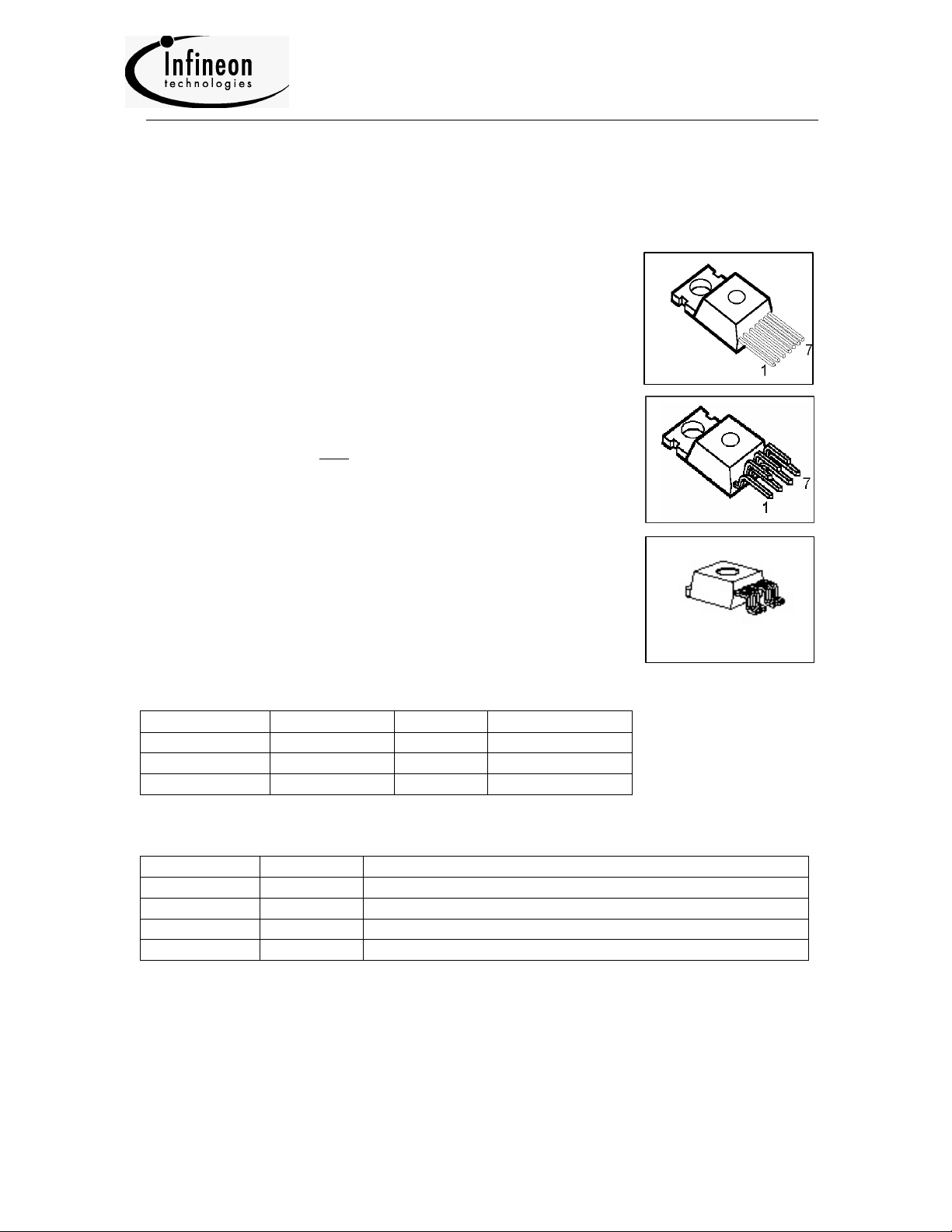
P-TO263
-7-2
Features
1 ... 3.3 V conversion:
phase PWM controller
P-TO220
-7-
230
Integrated Switch
Preliminary Data Sheet TDA21201
(MOSFET Driver and MOSFETs)
• Replaces with one part only the semiconductors of a DC/DC
power stage for a 12 V à
FET driver + High side FET + Low side FET
• Raises the efficiency by reducing static and dynamic losses
beyond 85 % due to optimized MOSFETs and Driver
• Reduces overall part count and board space consumption
• Simplifies and shortens the circuit design and the layout
P-TO220-7-3
• Eliminates the need for external bootstrap components
• Provides simplest overall output current scalability
• Protects the Driver and
the MOSFETs against over-
temperature and shoot-through problems Vcc à Gnd
• Achieves the lowest thermal resistance Rthjc and Rthja
• Uses the well-known, easy-to-assemble and robust
standard TO-220 and TO-263 (D²Pak) package
• Requires no separate supply voltage to operate except 12 V
• Three state input to enable a shut down mode to turn off
both MOSFETs
• Compatible with standard 2-, 3-, 4-, 6ICs
• Ideal for compact, highly-efficient, multi-phase voltage
regulators on motherboards and VRMs
7
1
Type Package Marking Ordering Code
TDA21201-P7 TO-220-7-3 21201P7 Q67042-S4100
TDA21201-S7 TO-220-7-230 21201S7 Q67042-S4101
TDA21201-B7 TO-263-7-2 21201B7 Q67042-S4099
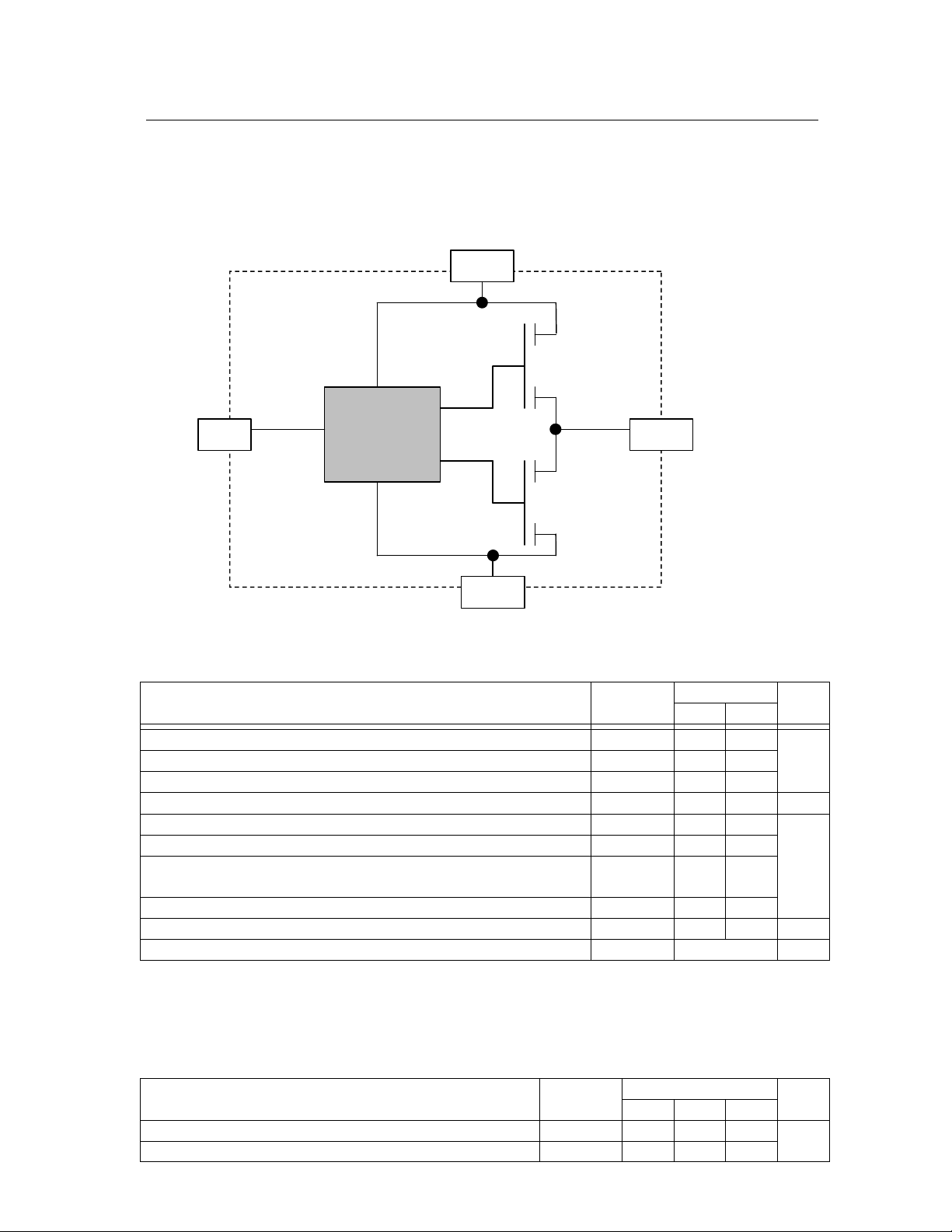
Pin Configuration and Function
Pin number Pin name Pin description
1,2,3 GND Ground
4/tab V
Output voltage from common node of the MOSFETs
OUT
5 IN Input signal from PWM controller
6,7 VCC Supply voltage to MOSFETs and Driver IC
General Description
The Integrated Switch TDA21201 incorporates an intelligent MOSFET driver and two
Power MOSFETs in a single package to form a fully integrated and optimized power
stage of a DC/DC synchronous buck converter including the bootstrap components
for the high-side MOSFET.
The Power MOSFETs are optimized for lowest static and dynamic losses for a 12 V
to sub-3.5 V conversion and can handle up to 30 A output current. The TDA21201 is
manufactured in Infineon´s state-of-the-art multi-chip assembly using a low-Rth 7-Pin
Page 1 Apr-29, 2002
Preliminary Data Sheet TDA21201
TO-220 package or its associated SMD counterpart TO-263 and Infineon´s latest
chip technologies.
Block Diagram
VCC
= 12 V (Pin 6-7)
High side FET
VIN
FET Drive
Circuitry
V
OUT
to PWM IC
(Pin 5)
Low side FET
to output inductor
(Pin 4/tab)
GND
(Pin 1-3)
Absolute Maximum Ratings
At Tj = 25 °C, unless otherwise specified
Parameter Symbol
Value
Unit
Min. Max.
Peak voltage supplied to ‘VCC’ pins V
Peak voltage supplied to ‘IN’ pin, D
< 10 % VIN -5 10
IN_Peak
Peak voltage at ‘Vout’ pin to GND V
Maximum DC output current, VCC = 12 V, V
≤ 3.3 V
OUT
CC_PEAK
OUT_PK
I
OUT_MAX
Junction temperature TJ 150
Storage temperature TS -55 150
Lead temperature TO-263;
TL 225
20*
-5 20*
-10 30 A
°C
V
MSL1, IPC/JEDEC J-STD-020A
Lead temperature TO-220 (soldering, 10 seconds) TL 260
ESD rating (Human body model) ESD 2 k V
IEC climatic category; DIN EN 60068-1 55/150/56 -
* The positive peak voltage (= the voltage overshoot during switching transients) at the VCC pins and
the OUT pin/tab is limited by the Integrated Switch itself (pls., see the “Over-voltage protection of
VCC” paragraph
Thermal Characteristic
Values Parameter Symbol
Unit
Min. Typ. Max.
Thermal resistance, junctions-case 1.9
Thermal resistance, junctions-ambient, leaded 62.5
Page 2 Apr-29, 2002
K/W
SMD version, device on PCB:
@ min. footprint
@ 6 cm² cooling area
Preliminary Data Sheet TDA21201
62
40
Electrical Characteristics
At Tj = 25 °C, unless otherwise specified
Parameter Symbol
Conditions
Min.
Values
Typ. Max.
Unit
Input Characteristic (= MOSFET Driver)
Shut down window V
Shut down hold-off
IN_SHUT
t_
SHUT
t_
1.2 V ≤ V
> 1.5 µs 1.2 1.6 V
SHUT
≤ 1.6 V
IN
0.8 1.5 2.5 µs
time
Supply current during
shut down
Current into ‘IN’ pin,
during shut down
Current into ‘IN’ pin,
I
CC_SHUT
I
IN_SHUT
I
IN_LOW
1.2 V ≤ V
≤ 1.6 V
IN
10 16 22 mA
VCC = 12 V
VIN = 1.4 V -10 10
VIN = 0.4 V -2 -10 -50
µA
Low
Current into ‘IN’ pin,
I
IN_HIGH
VIN = 4.5 V 20 35 80
High
Static Characteristic (= High Side and Low Side MOSFET)
D-S Breakdown
Voltage High Side
D-S Breakdown
DS_HS
V
DS_LS
1.2 V ≤ V
I
D
≤ 1.6 V
IN
= 0.25 A
30
V
V
Voltage Low Side
D-S Leakage Current
High Side
D-S Leakage Current
High Side
Drain-Source on
Resistance High Side
Drain-Source on
Resistance Low Side
Drain-Source on
Resistance High Side
Drain-Source on
I
DSS_HS
I
DSS_LS
R
DSon_HS
R
DSon_LS
R
DSon_HS
R
DSon_LS
1.2 V ≤ V
V
CC
≤ 1.6 V
IN
= 12 V
I
= 15 A
OUT
Tj = 25 °C
I
= 15 A
OUT
Tj = 125 °C
0.1 1 µA
13.3
4.8
17.7
6.4
mΩ
Resistance Low Side
Dynamic Characteristic (= Integrated Switch)
IN to OUT delay time
L à H; 50 % to 50 %
IN to OUT delay time
H à L; 50 % to 50 %
OUT rise time; 20 %
t
110 150
d(ON)
= 15 A
t
70 100
d(OFF)
I
OUT
tr 10 25
(s. Timing Diagram)
ns
to 80 %
OUT fall time; 80 to
tf
10 30
20 %
Page 3 Apr-29, 2002
t
d(on)
t
d(off)
VIN
V
OUT
t
d(on)
t
d(off)
Preliminary Data Sheet TDA21201
Operating Conditions
At Tj = 25 °C, unless otherwise specified
Parameter Symbol
Voltage supplied to
VCC 9 15
‘VCC’ pins
Voltage ‘IN’ Low V
Voltage ‘IN’ High V
Input signal transition
-0.5 0.8
IN_L
2.1 5.5
IN_H
f 100 500 KHz
Conditions
Min.
Values
Typ. Max.
Unit
V
frequency
Pulse width Input t
Power dissipation P
90 ns
P_IN
10 W
TOT
Junction temperature TJ -25 125 °C
Timing Diagram
50%
50%
Typical application
A circuit designer will value the Integrated Switch TDA21201 as cost-optimized
power stage solution in high-density DC/DC conversion applications using a Vcc = 12
V input where efficiency and board space is an issue, e.g. in multi-phase
microprocessor supplies on motherboards, in VRMs and servers.
The TDA21201 can also be used to power Logic circuits, Memory banks etc. that
require higher voltages, e.g. 2.5 or 3.3 V. The efficiency of the Integrated Switch and
the overall efficiency of the converter will even go up at these elevated output
voltages compared to the 1.6 V efficiency given later on in this data sheet.
Page 4 Apr-29, 2002
PWM 1
1
N
N
C
Preliminary Data Sheet TDA21201
Designing a 12 V to sub-3.3 V converter using the TDA21201
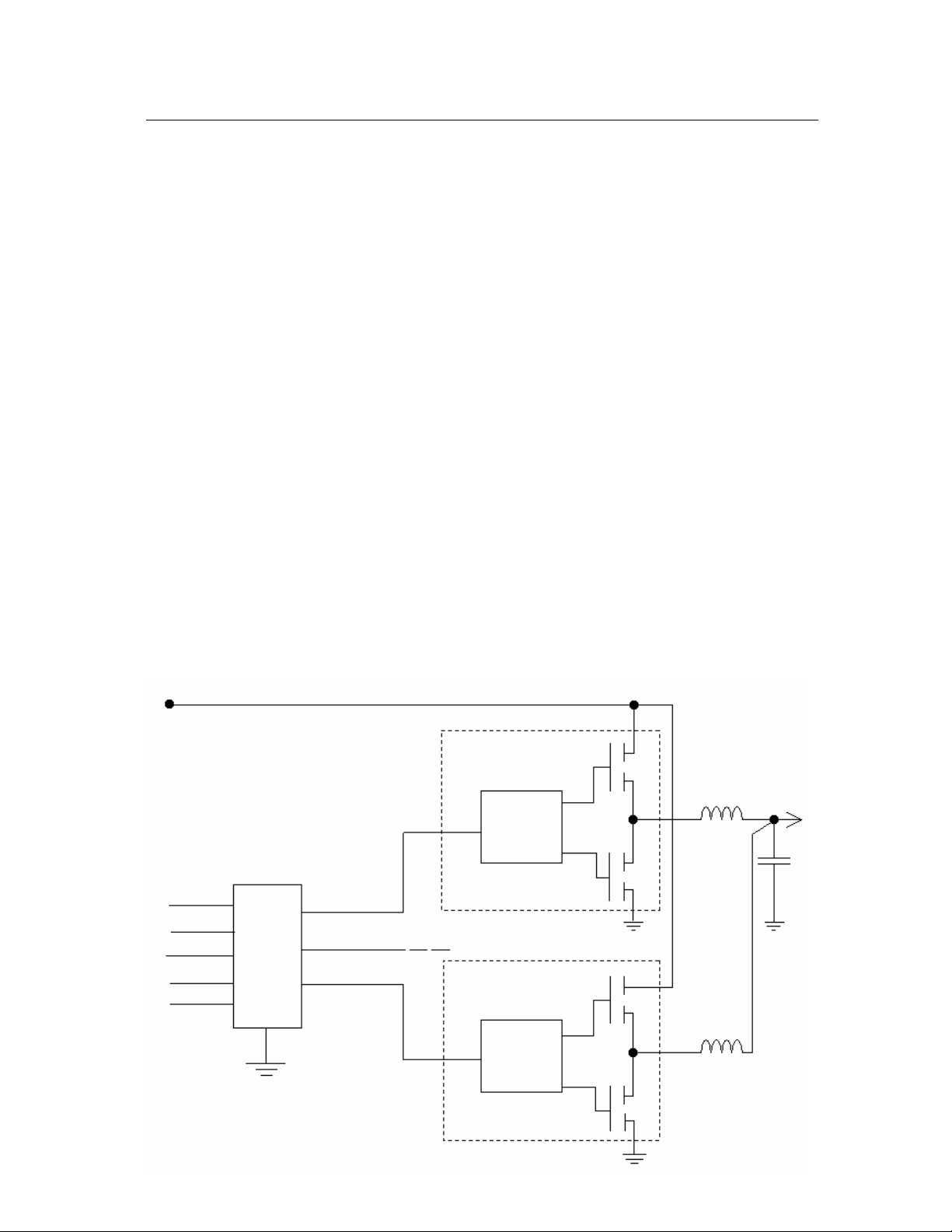
General info
To design a multi-phase converter with a 12 V input simply use in each phase
just one TDA21201 instead of using a MOSFET driver, a high side MOSFET,
bootstrap components, and one or more low side MOSFETs. The entire
converter is completed by the input filter, the output filter and a multi-phase
PWM IC.
Input compatibility to standard PWM controllers / shut-down mode
The Integrated Switch TDA21201 has a high impedance input pin ‘IN’ to be
connected to PWM controller outputs ‘PWM1’, ‘PWM2’ etc. It sinks or sources
only a fraction of a mA from the controller’s output. The TDA21201 is
compatible to standard controller and driver signals in terms of the signal level
(5 V TTL) and in terms of the ‘Low’/’High’ relationship (’Low’ turns the low side
MOSFET on, ‘High` turns the High side MOSFET on).
The TDA21201 can be shut down (the high side MOSFET and the low side
MOSFET is turned off) by applying an input signal V
= 1.2 ... 1.6 V for more
IN
than 1.5 µs typical. This way the TDA21201 reduces the power dissipation by
saving the gate charges of both the high side and the low side MOSFET
during no load conditions. The shutdown state is terminated when V
moves
IN
into the ‘Low’ or ‘High’ threshold.
Typical Application: 12 V à 1.x V N-Phase Converter using the TDA21201
12 V
L1
1...2 V
FET
Driver
PWM
IC
PWM 2
PWM N
L
FET
Driver
Page 5 Apr-29, 2002

C
I I I
I
I
turn ON
turn ON
Integ
rated
Preliminary Data Sheet TDA21201
12 V
VCC
IN
TDA
L1
OUT
1...2 V
21201
PWM 1
PWM
IC
PWM 2
PWM N
GND
TDA
L
N
21201
Integrated Switch functionality vs. supply voltage Vcc
Switch
function
Low Side
FET can
Integrated Switch OFF
6 V 7.5 V 9 V 12 V 15 V Vcc
High Side
FET can
Integrated Switch fully
functional
The Integrated Switch reaches gradually its full functionality while the supply
voltage Vcc increases from 0 to its nominal value +12 V, e.g. during turn-on.
The same happens vice versa when the supply voltage decreases from its
nominal value +12 V to 0, e.g. during turn-off. The TDA21201 is very
insensitive to Vcc tolerances. It behaves properly in a wide Vcc range from 9
to 15 V. There is no distinct V
functionality or state changes abrupt while V
threshold at which the Integrated Switch’s
CC
increases or decreases. E.g.,
CC
there is no tight specified Under Voltage Lockout level. The TDA21201
changes smoothly its state, e.g., as the High Side and Low Side MOSFETs´
gate drive voltage increases while V
increases from 7.5 V to 9 V the Rds[on]
CC
of both the High Side MOSFET and the Low Side MOSFET decreases
gradually, rather than being fully Off at VCC slightly below a threshold level or
Page 6 Apr-29, 2002

Preliminary Data Sheet TDA21201
being fully On at a VCC level slightly greater than the threshold.
Bootstrapping
Turning on and off the High side MOSFET is done internally by the Driver. The
TDA21201 does not require any external bootstrap components such as a
capacitor or diode. Just apply GND, Vcc = 12 V, and the PWM signal of the
Controller to it and the Integrated Switch will operate.
Input filter / Output filter / Converter Stability
The Integrated Switch TDA21201 is a new solution to implement the power
semiconductor components in a DC/DC converter. It offers many advantages
to the user. However, the basic behavior with respect to the voltages, the
currents and the timing remains unchanged. Therefore, any of the rules and
procedures applied to design DC/DC converters using discrete MOSFETs and
Drivers apply in the same way to converters using the Integrated Switch –
except the worries regarding dead time control, lowest impedance in the AC
loop, elevated driver temperatures etc.
Current sense
Any of the commonly used current sense techniques are supported by the
Integrated Switch. For Low side sensing measure the voltage drop across the
GND pins and the OUT pin (or the tab when using the SMD version) during
the Low side switch’s On-time (Vin = Low). The High side MOSFET is sensed
across the Vcc and the OUT pin (or the tab when using the SMD version) of
the Integrated Switch during its On-time (Vin = High). Inductor sensing is
implemented outside of the integrated switch the usual way.
Resistor sensing using a separate resistor in the Input capacitor à High side
MOSFET (Vcc pin) path is possible but not recommended
. This current sense
approach introduces ample stray inductance in the AC current loop (+terminal
of the input capacitor à High side MOSFET à Low side MOSFET à GND à
-terminal of the input capacitor). This results in a very noisy Vcc line especially
during the switching period and a non-optimized switching behavior of the
Integrated Switch. This in turn, increases the switching losses and the device
temperature and lowers the efficiency.
Output current scalability
The converter output current can be chosen in a wide range by selecting the
appropriate number of phases. At a given number of phases the current per
phase (= current per TDA21201) and in turn the overall converter output
current is set by application requirements, e.g. the switching frequency, and by
environmental conditions, e.g. ambient temperature and the thermal
resistance of the TDA21201 to ambient. As a reference, one TDA21201
generates roughly 3.2 W @ 15 A RMS and 250 kHz (V
= 12 V, VO = 1.6 V).
CC
This amount of loss can be dissipated by the SMD version of the Integrated
Switch on a regular motherboard using proper thermal design techniques.
Greater phase currents result in higher losses; and higher switching
Page 7 Apr-29, 2002

Preliminary Data Sheet TDA21201
frequencies will also result in more losses. So, in modifying the thermal
environment and a switching frequency the phase current can be matched
your requirements; please, consult the efficiency curves in this Data Sheet to
choose the most suitable phase current and switching frequency per phase for
a particular design. To give a circuit designer more freedom in scaling the
phase current, the Integrated Switch is offered in a heat sink capable TO-220
version that allows better thermal coupling to ambient and a higher junction
temperature in the Integrated Switch as well - without violating the applicable
regulations.
Over temperature shut-down
The over temperature shut-down function of the Integrated Switch takes effect
@ 150 °C junction temperature typically and turns off the High side MOSFET
and the Low side MOSFET. Unlike as in discrete converter solutions the
MOSFETs and the Driver are thermally very well coupled. Therefore, this
function protects the Driver and
the MOSFETs. Once the Integrated Switch is
cooled down and the temperature shut-down is released the Integrated Switch
continues to operate by turning on one of the MOSFETs according to its PWM
signal present on the input.
Under Voltage Lockout / ∆ Vcc detection
The TDA21201 is fully functional at Vcc ≥ 9 V. However, the Low side
MOSFET can already be turned on at Vcc ≈ 6 V or greater when the input is
Low. The Integrated Switch is disabled and both MOSFETs are turned off at
lower Vcc, e.g. during power-up of the ATX supply.
The TDA21201 has two paralleled Vcc pins. The voltage applied to these pins
will be converted to a lower output voltage but it also serves as supply voltage
of the integrated gate drive circuit. Therefore, the voltage difference ∆ Vcc is
monitored for safety reasons. When ∆ Vcc ≥ 0.45 V for more than 2 µs
typically the Integrated Switch is disabled. This way it prevents the part itself
but it also protects the load
from inadequate behavior, e.g. due to a bad
soldering connection of the Vcc pins.
Layout guidelines
In general, the layout is simplified when using the Integrated Switch. However,
it should be kept in mind that the power density in the Integrated Switch is
higher than in a discrete solution. Therefore, proper thermal layout is very
critical in designs that employ the SMD version.
Another important aspect is a very low impedance path in the Vcc = 12 V à
TDA21201 à GND loop. It is recommended to place the capacitors of the
input filter as close to the GND and Vcc pins of the TDA21201 as possible.
Additional ceramic capacitors in parallel to the input capacitors help to reduce
the effect of stray inductance of the input capacitors and the PCB traces.
Reducing parasitic inductance will result in an optimized switching behavior
and lower switching losses. The arrangement of the output filter is of second
order importance.
Page 8 Apr-29, 2002

V
< 20
HS is turned off
Preliminary Data Sheet TDA21201
Over voltage protection of Vcc / Avalanche avoidance
The voltage at the Vcc pins of the TDA21201 rises above the nominal DC
value of the Vcc supply (= + 12 V) during the turn-off of the High Side
MOSFET. The voltage overshoots at the Vcc pins according to:
vcc(t) = Vcc + Lstray * di/dt
vcc (t) = instantaneous value of vcc; Vcc = +12 V DC; Lstray = stray
inductance of the PCB traces + the input capacitor’s ESL + the parasitic
inductance of the TDA21201 package itself; di/dt = slew rate of the High Side
current during its turn-off.
V
= +12 V
cc
TDA21201
L
stray
v
cc
HS C
L
D
z
Driver
in
out
LS
This equation reveals that Lstray should be made as small as possible (as
vcc(t) is limited by the breakdown voltage of the device, Vcc is given by the
application, di/dt should be as large as possible to reduce switching losses)
using proper layout techniques and low ESL capacitors, e.g. ceramics,
between the Vcc and GND pins of the Integrated Switch.
To protect the Integrated Switch from unallowable voltage spikes, the slew rate
of the High Side current di/dt is controlled in a way so that the overall voltage
(between Vcc pins to GND pins) does not exceed 20 V (measured between
the Vcc and GND pins at the PCB, this voltage will slightly exceed the 20 V
limit within the package/at the chips). As the MOSFETs have a Breakdown
voltage rating Vds = 30 V, it is made sure that they are never driven into
avalanche.
The slew rate control is implemented using the principal of the active zener
clamp technique: When vcc(t) rises during turn-off then the effective gate-drain
voltage of the High Side MOSFET rises, too. If, for what reason ever, the vcc(t)
overshoot approaches a value that possibly could damage the integrated
Page 9 Apr-29, 2002
t

Preliminary Data Sheet TDA21201
driver or the MOSFETs, the zener diode becomes conducting and reduces the
discharge speed of the High Side MOSFET´s gate within nanoseconds. This
will reduce slightly the turn-off slew rate of the High Side MOSFET´s current (=
di/dt). As a result the over voltage will be limited.
Power loss in the Integrated Switch TDA21201 / Heat sink estimation
The power loss in the Integrated Switch depends mainly on the current and
the switching frequency. Other conditions that impact the power loss are
increased junction temperature and the layout (e.g. very tight coupling of the
input capacitor to the V
and GND pins to reduce the PCB trace inductance).
CC
6
5
4
3
Pd [W]
2
Iphase =12 A Iphase =18 A
1
100 150 200 250 300 350 400 450
f_sw / phase [kHz]
6
f_sw = 100 kHz
5
4
Pd [W]
3
2
1
10 15 20 25
Iphase [A]
f_sw = 150 kHz
f_sw = 200 kHz
f_sw = 250 kHz
f_sw = 300 kHz
Using the above two diagrams the power loss (= the required power
dissipation Pd for thermally stable operation) can be estimated based on a
required phase current Iphase (= current in the Integrated Switch) an based on
the switching frequency per phase f_sw (= frequency of the Integrated Switch
in each phase).
Page 10 Apr-29, 2002

Pd
−
Efficiency [%]
Preliminary Data Sheet TDA21201
Having the power dissipation Pd of the Integrated Switch, the required thermal
resistance RthCA can be calculated. RthCA is the value of the heat sink
attached to the TO-220 version of the Integrated Switch. RthCA is the
“effective” thermal resistance (takes airflow etc. into account):
TATj
RthCA −
max_
≤
Rthjc
Wherein: R
CA = Thermal resistance from the package’s metal backside
th
(= lead frame) to ambient air that is required to operate the
Integrated Switch under given load and environmental
conditions without exceeding the maximum allowed
junction temperature; in [°C/W]
T
= Maximum allowed junction temperature of the Integrated
j_max
Switch; in [°C], use 110 °C for the SMD version of the
Integrated Switch, use 125 °C for the TO-220 version of
the Integrated Switch
TA = The ambient temperature; in [°C], usually this is the
maximum temperature of the surrounding air @ worst
case, e.g. 55 °C
Pd = The power loss generated in the Integrated Switch that
needs to be dissipated through the heat sink à air
(TO-220) or the PCB à air for thermal balance; in [W], use
one of the two diagrams Pd vs. Iphase or Pd vs. f_sw to
find the this value for your particular application
R
jc = Thermal resistance junction to case of the Integrated Switch;
th
in [K/W], use ≤ 2 K/W (s. also pg. 3 and 4 “Thermal
characteristic of the High side/Low side MOSFET” in this
data sheet; the majority of the losses are generated within
the MOSFETs, not in the driver)
Efficiency of a DC/DC converter using the Integrated Switch TDA21201
The following measurements were performed on a 4-phase Evaluation Board.
Phase 4 can be disabled so that the converter operates in a 3-phase mode.
Boundary Conditions: Vcc = 12 V, Vo = 1.6 V, TDA21201 as SMD
I 4-Phase Converter: Efficiency vs. Load current
95
90
85
80
75
70
65
0 20 40 60 80
Page 11 Apr-29, 2002
Load Current [A]
f_1 = 185 kHz
f_2 = 305 kHz

Efficiency [%]
Preliminary Data Sheet TDA21201
II 4-Phase Converter: Efficiency vs. Switching frequency
95
90
85
80
75
150 200 250 300 350
Frequency / Phase [kHz]
Io_1 = 25 A
Io_2 = 40 A
Io_3 = 55 A
Io_4 = 70 A
Ill 3- and 4-Phase Converter: Efficiency vs. Load current
95
90
85
80
Efficiency [%]
75
70
4 Phase @ 185 kHz
4 Phase @ 305 kHz
3 Phase @ 185 kHz
3 Phase @ 305 kHz
65
0 10 20 30 40 50 60
Load current [A]
It should be noted that the overall converter efficiency and the maximum converter
output power will increase as the output voltage increases, e.g. V
= 2.5 or 3.3 V.
O
Page 12 Apr-29, 2002

Preliminary Data Sheet TDA21201
Package Drawing TO-220-7-3 (straight leads)
Package Drawing TO-220-7-230 (staggered leads)
Page 13 Apr-29, 2002

Preliminary Data Sheet TDA21201
Package Drawing TO-263-7-2 (SMD)
Page 14 Apr-29, 2002

Published by
Infineon Technologies AG,
Bereichs Kommunikation
St.-Martin-Strasse 53,
D-81541 München
Infineon Technologies AG 1999
All Rights Reserved.
Attention please!
The information herein is given to describe certain components and shall not be considered as warranted
Characteristics.
Terms of delivery and rights to technical change reserved.
We hereby disclaim any and all warranties, including but not limited to warranties of non-infringement,
regarding circuits, descriptions and charts stated herein.
Infineon Technologies is an approved CECC manufacturer.
Information
For further information on technology, delivery terms and conditions and prices please contact your
nearest Infineon Technologies Office in Germany or our Infineon Technologies Representatives
worldwide (see address lists).
Warnings
Due to technical requirements components may contain dangerous substances.
For information on the types in question please contact your nearest Infineon Technologies Office.
Infineon Technologies Components may only be used in life-support devices or systems with the
express written approval of Infineon Technologies, if a failure of such components can reasonably be
expected to cause the failure of that life-support device or system, or to affect the safety or
effectiveness of that device or system Life support devices or systems are intended to be implanted in
the human body, or to support and/or maintain and sustain and/or protect human life. If they fail, it is
reasonable to assume that the health of the user or other persons may be endangered.
Preliminary Data Sheet TDA21201
Page 15 Apr-29, 2002
 Loading...