


Data Sheet, V0.1, Nov. 2005
TC1161/TC1162
32-Bit Single-Chip Microcontroller
TriCore
TM
Microcontrollers
Never stop thinking.

Edition 2005-11
Published by Infineon Technologies AG,
St.-Martin-Strasse 53,
81669 München, Germany
© Infineon Technologies AG 2005.
All Rights Reserved.
Attention please!
The information herein is given to describe certain components and shall not be considered as a guarantee of
characteristics.
Terms of delivery and rights to technical change reserved.
We hereby disclaim any and all warranties, including but not limited to warranties of non-infringement, regarding
circuits, descriptions and charts stated herein.
Information
For further information on technology, delivery terms and conditions and prices please contact your nearest
Infineon Technologies Office (www.infineon.com).
Warnings
Due to technical requirements components may contain dangerous substances. For information on the types in
question please contact your nearest Infineon Technologies Office.
Infineon Technologies Components may only be used in life-support devices or systems with the express written
approval of Infineon Technologies, if a failure of such components can reasonably be expected to cause the failure
of that life-support device or system, or to affect the safety or effectiveness of that device or system. Life support
devices or systems are intended to be implanted in the human body, or to support and/or maintain and sustain
and/or protect human life. If they fail, it is reasonable to assume that the health of the user or other persons may
be endangered.

Data Sheet, V0.1, Nov. 2005
TC1161/TC1162
32-Bit Single-Chip Microcontroller
TriCore
TM
Microcontrollers
Never stop thinking.

TC1161/TC1162 Data Sheet
Revision History: V0.1, 2005-11
Previous Version: none
Page Subjects (major changes since last revision)
Trademarks
TriCore™ is a trademark of Infineon Technologies AG.
We Listen to Your Comments
Any information within this document that you feel is wrong, unclear or missing at all?
Your feedback will help us to continuously improve the quality of this document.
Please send your proposal (including a reference to this document) to:
mcdocu.comments@infineon.com
Template: mc_a5_um_tmplt.fm / 4 / 2004-09-15

TC1161/TC1162
Table of ContentsAdvance Information
Table of Contents
1 Summary of Features . . . . . . . . . . . . . . . . . . . . . . . . . . . . . . . . . . . . . . . . 3
2 General Device Information . . . . . . . . . . . . . . . . . . . . . . . . . . . . . . . . . . . 6
2.1 Block Diagram . . . . . . . . . . . . . . . . . . . . . . . . . . . . . . . . . . . . . . . . . . . . . . . 6
2.2 Logic Symbol . . . . . . . . . . . . . . . . . . . . . . . . . . . . . . . . . . . . . . . . . . . . . . . . 7
2.3 Pin Configuration . . . . . . . . . . . . . . . . . . . . . . . . . . . . . . . . . . . . . . . . . . . . . 8
2.4 Pad Driver and Input Classes Overview . . . . . . . . . . . . . . . . . . . . . . . . . . . 9
2.5 Pin Definitions and Functions . . . . . . . . . . . . . . . . . . . . . . . . . . . . . . . . . . 10
3 Functional Description . . . . . . . . . . . . . . . . . . . . . . . . . . . . . . . . . . . . . . 24
3.1 System Architecture and On-Chip Bus Systems . . . . . . . . . . . . . . . . . . . . 24
3.2 On-Chip Memories . . . . . . . . . . . . . . . . . . . . . . . . . . . . . . . . . . . . . . . . . . . 25
3.3 Memory Maps . . . . . . . . . . . . . . . . . . . . . . . . . . . . . . . . . . . . . . . . . . . . . . 27
3.3.1 Architectural Address Map . . . . . . . . . . . . . . . . . . . . . . . . . . . . . . . . . . . 27
3.3.2 How to Read the Address Maps . . . . . . . . . . . . . . . . . . . . . . . . . . . . . . 29
3.3.3 Contents of the Segments . . . . . . . . . . . . . . . . . . . . . . . . . . . . . . . . . . . 30
3.3.4 Address Map of the FPI Bus System . . . . . . . . . . . . . . . . . . . . . . . . . . . 32
3.3.4.1 Segments 0 to 14 . . . . . . . . . . . . . . . . . . . . . . . . . . . . . . . . . . . . . . . . 32
3.3.4.2 Segment 15 . . . . . . . . . . . . . . . . . . . . . . . . . . . . . . . . . . . . . . . . . . . . 37
3.3.5 Address Map of the Local Memory Bus (LMB) . . . . . . . . . . . . . . . . . . . 42
3.4 Memory Protection System . . . . . . . . . . . . . . . . . . . . . . . . . . . . . . . . . . . . 46
3.5 DMA Controller and Memory Checker . . . . . . . . . . . . . . . . . . . . . . . . . . . . 47
3.6 Interrupt System . . . . . . . . . . . . . . . . . . . . . . . . . . . . . . . . . . . . . . . . . . . . 49
3.7 Asynchronous/Synchronous Serial Interfaces (ASC0, ASC1) . . . . . . . . . . 51
3.8 High-Speed Synchronous Serial Interfaces (SSC0) . . . . . . . . . . . . . . . . . 53
3.9 Micro Second Bus Interfaces (MSC0) . . . . . . . . . . . . . . . . . . . . . . . . . . . . 55
3.10 MultiCAN Controller (CAN) . . . . . . . . . . . . . . . . . . . . . . . . . . . . . . . . . . . . 57
3.11 Micro Link Serial Bus Interface (MLI0) . . . . . . . . . . . . . . . . . . . . . . . . . . . . 59
3.12 General Purpose Timer Array . . . . . . . . . . . . . . . . . . . . . . . . . . . . . . . . . . 61
3.12.1 Functionality of GPTA0 . . . . . . . . . . . . . . . . . . . . . . . . . . . . . . . . . . . . . 62
3.13 Analog-to-Digital Converter (ADC0) . . . . . . . . . . . . . . . . . . . . . . . . . . . . . 65
3.14 Fast Analog-to-Digital Converter Unit (FADC) . . . . . . . . . . . . . . . . . . . . . . 67
3.15 System Timer . . . . . . . . . . . . . . . . . . . . . . . . . . . . . . . . . . . . . . . . . . . . . . . 69
3.16 Watchdog Timer . . . . . . . . . . . . . . . . . . . . . . . . . . . . . . . . . . . . . . . . . . . . 71
3.17 System Control Unit . . . . . . . . . . . . . . . . . . . . . . . . . . . . . . . . . . . . . . . . . . 72
3.18 Boot Options . . . . . . . . . . . . . . . . . . . . . . . . . . . . . . . . . . . . . . . . . . . . . . . 73
3.19 Power Management System . . . . . . . . . . . . . . . . . . . . . . . . . . . . . . . . . . . 74
3.20 On-Chip Debug Support . . . . . . . . . . . . . . . . . . . . . . . . . . . . . . . . . . . . . . 75
3.21 Clock Generation and PLL . . . . . . . . . . . . . . . . . . . . . . . . . . . . . . . . . . . . . 77
3.22 Power Supply . . . . . . . . . . . . . . . . . . . . . . . . . . . . . . . . . . . . . . . . . . . . . . . 80
3.23 Identification Register Values . . . . . . . . . . . . . . . . . . . . . . . . . . . . . . . . . . 81
Data Sheet 1 V0.1, 2005-11

TC1161/TC1162
Table of ContentsAdvance Information
4 Electrical Parameters . . . . . . . . . . . . . . . . . . . . . . . . . . . . . . . . . . . . . . . 82
4.1 General Parameters . . . . . . . . . . . . . . . . . . . . . . . . . . . . . . . . . . . . . . . . . 82
4.1.1 Parameter Interpretation . . . . . . . . . . . . . . . . . . . . . . . . . . . . . . . . . . . . 82
4.1.2 Pad Driver and Pad Classes Summary . . . . . . . . . . . . . . . . . . . . . . . . . 83
4.1.3 Absolute Maximum Ratings . . . . . . . . . . . . . . . . . . . . . . . . . . . . . . . . . . 84
4.1.4 Operating Conditions . . . . . . . . . . . . . . . . . . . . . . . . . . . . . . . . . . . . . . . 85
4.2 DC Parameters . . . . . . . . . . . . . . . . . . . . . . . . . . . . . . . . . . . . . . . . . . . . . 88
4.2.1 Input/Output Pins . . . . . . . . . . . . . . . . . . . . . . . . . . . . . . . . . . . . . . . . . . 88
4.2.2 Analog to Digital Converter (ADC0) . . . . . . . . . . . . . . . . . . . . . . . . . . . . 91
4.2.3 Fast Analog to Digital Converter (FADC) . . . . . . . . . . . . . . . . . . . . . . . . 98
4.2.4 Oscillator Pins . . . . . . . . . . . . . . . . . . . . . . . . . . . . . . . . . . . . . . . . . . . 102
4.2.5 Temperature Sensor . . . . . . . . . . . . . . . . . . . . . . . . . . . . . . . . . . . . . . 103
4.2.6 Power Supply Current . . . . . . . . . . . . . . . . . . . . . . . . . . . . . . . . . . . . . 104
4.3 AC Parameters . . . . . . . . . . . . . . . . . . . . . . . . . . . . . . . . . . . . . . . . . . . . 105
4.3.1 Testing Waveforms . . . . . . . . . . . . . . . . . . . . . . . . . . . . . . . . . . . . . . . 105
4.3.2 Output Rise/Fall Times . . . . . . . . . . . . . . . . . . . . . . . . . . . . . . . . . . . . 106
4.3.3 Power Sequencing . . . . . . . . . . . . . . . . . . . . . . . . . . . . . . . . . . . . . . . . 107
4.3.4 Power, Pad and Reset Timing . . . . . . . . . . . . . . . . . . . . . . . . . . . . . . . 109
4.3.5 Phase Locked Loop (PLL) . . . . . . . . . . . . . . . . . . . . . . . . . . . . . . . . . . 111
4.3.6 Debug Trace Timing . . . . . . . . . . . . . . . . . . . . . . . . . . . . . . . . . . . . . . 112
4.3.7 Peripheral Timings . . . . . . . . . . . . . . . . . . . . . . . . . . . . . . . . . . . . . . . . 113
4.3.7.1 Micro Link Interface (MLI) Timing . . . . . . . . . . . . . . . . . . . . . . . . . . 113
4.3.7.2 Micro Second Channel (MSC) Interface Timing . . . . . . . . . . . . . . . 115
4.3.7.3 Synchronous Serial Channel (SSC) Master Mode Timing . . . . . . . . 116
5 Packaging . . . . . . . . . . . . . . . . . . . . . . . . . . . . . . . . . . . . . . . . . . . . . . . . 117
5.1 Package Parameters . . . . . . . . . . . . . . . . . . . . . . . . . . . . . . . . . . . . . . . . 117
5.2 Package Outline . . . . . . . . . . . . . . . . . . . . . . . . . . . . . . . . . . . . . . . . . . . 118
5.3 Flash Memory Parameters . . . . . . . . . . . . . . . . . . . . . . . . . . . . . . . . . . . 119
5.4 Quality Declaration . . . . . . . . . . . . . . . . . . . . . . . . . . . . . . . . . . . . . . . . . 120
Data Sheet 2 V0.1, 2005-11

TriCore
TC1161/TC116232-Bit Single-Chip Microcontroller
TM
Data Sheet 3 V0.1, 2005-11

TC1161/TC1162
Summary of FeaturesAdvance Information
– One General Purpose Timer Array Module (GPTA) with a powerful set of digital
signal filtering and timer functionality to realize autonomous and complex
Input/Output management
– One 16-channel Analog-to-Digital Converter unit (ADC) with selectable 8-bit, 10-
bit, or 12-bit, supporting 32 input channels
– One 2-channel Fast Analog-to-Digital Converter unit (FADC) with concatenated
comb filters for hardware data reduction: supporting 10-bit resolution, with
minimum conversion time of 318.2 ns
• 32 analog input lines for ADC and FADC
• 81 digital general purpose I/O lines
• Digital I/O ports with 3.3 V capability
• On-chip debug support for OCDS Level 1 and 2 (CPU, DMA)
• Power Management System
• Clock Generation Unit with PLL
• Core supply voltage of 1.5 V
• I/O voltage of 3.3 V
• Full Industrial and Multi-Market temperature range: -40° to +85°C
• PG-LQFP-176-2 package
Data Sheet 4 V0.1, 2005-11

TC1161/TC1162
Summary of FeaturesAdvance Information
Ordering Information
The ordering code for Infineon microcontrollers provides an exact reference to the
required product. This ordering code identifies:
• The derivative itself, i.e. its function set, the temperature range, and the supply
voltage
• The package and the type of delivery
For the available ordering codes for the TC1161/TC1162, please refer to the “Product
Catalog Microcontrollers” that summarizes all available microcontroller variants.
This document describes the derivatives of the device. Table 1-1 enumerates these
derivatives and summarizes the differences.
Table 1-1 TC1161/TC1162 Derivative Synopsis
Derivative Ambient Temperature Range
SAF-TC1161-128F66HL T
SAF-TC1162-128F66HL T
= -40oC to +85oC
A
= -40oC to +85oC
A
Data Sheet 5 V0.1, 2005-11
General Device InformationAdvance Information
2 General Device Information
Chapter 2 provides the general information for the TC1161/TC1162.
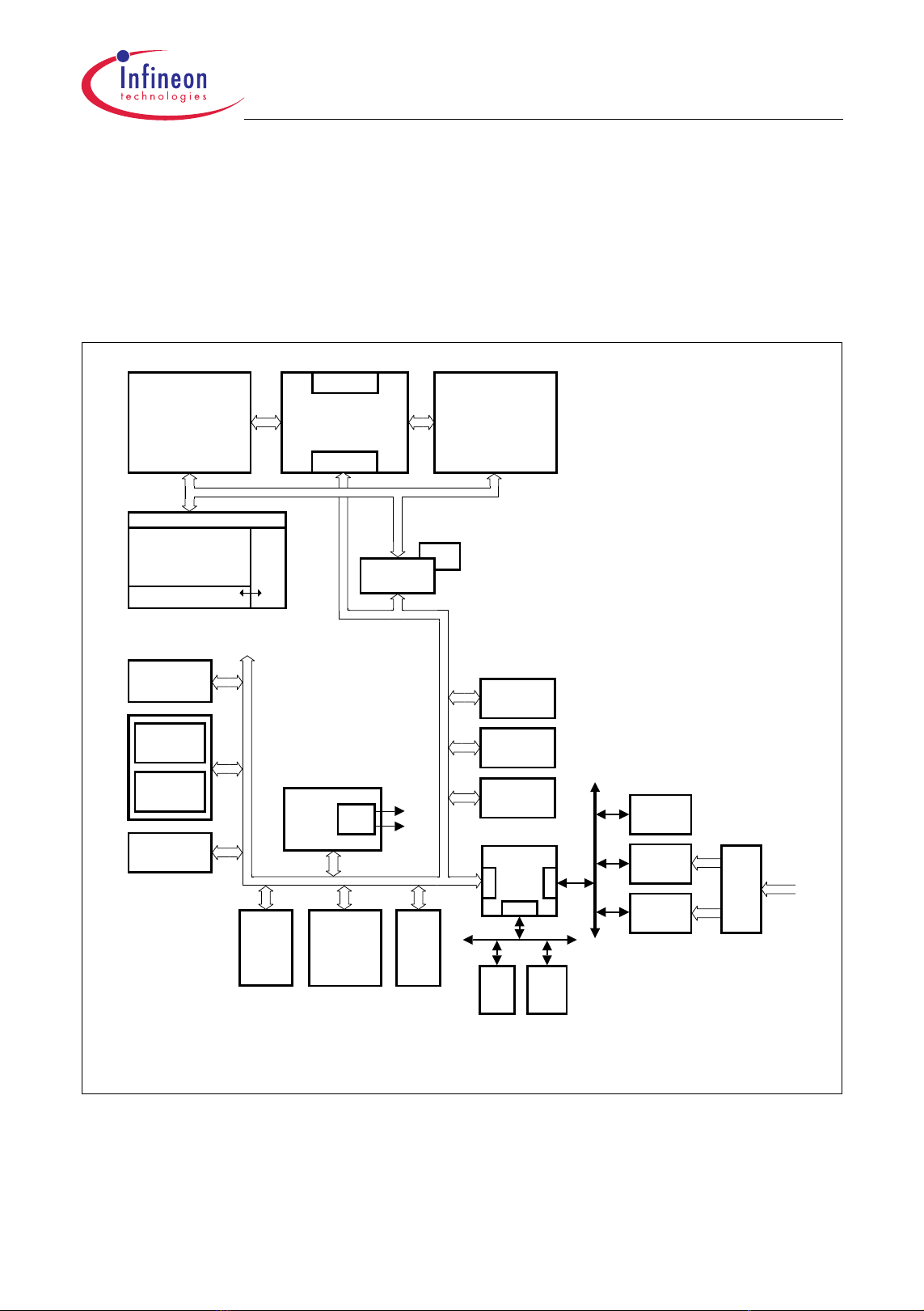
2.1 Block Diagram
Figure 2-1 shows the TC1161/TC1162 block diagram.
TC1161/TC1162
PMI
8 KB SP RAM
8 KB ICACHE
PMU
16 KB BROM
1024 KB Pf las h
16 KB DFlash
4 KB O VRAM
OCDS Debug
Interface/JTAG
ASC0
ASC1
GPTA
Overlay
System Peripheral Bus (SPB)
Ext.
Request
Unit
Me chan ism
FPU
TriCore
(TC1.3M)
CPS
PLL SCU PLL
Multi CAN
(2 Nodes ,
64 Buffer)
Local Memory Bus (LMB)
LBCU
LFI Bridge
f
FP I
f
CPU
1)
MSC0
DMI
32 KB LDRAM
STM
SBCU
Ports
DMA
8 ch.
BI0
SMIF
MLI0
Mem
Check
Abbr eviat ions:
ICACHE: Instruction Cache
SPRAM: Scratch-Pad RAM
LDRAM : Local Dat a RAM
OVRAM: Overlay RAM
BRO M: Boot RO M
PF lash: Program Flash
DFlash: Dat a F lash
SSC0
DMA Bus
BI1
ADC0
32 ch.
FADC
2 ch.
As si gnme nt
Analog Input
1) Not applicable to TC1161
TC1161/TC1162 Block Diagram
Figure 2-1 TC1161/TC1162 Block Diagram
Data Sheet 6 V0.1, 2005-11
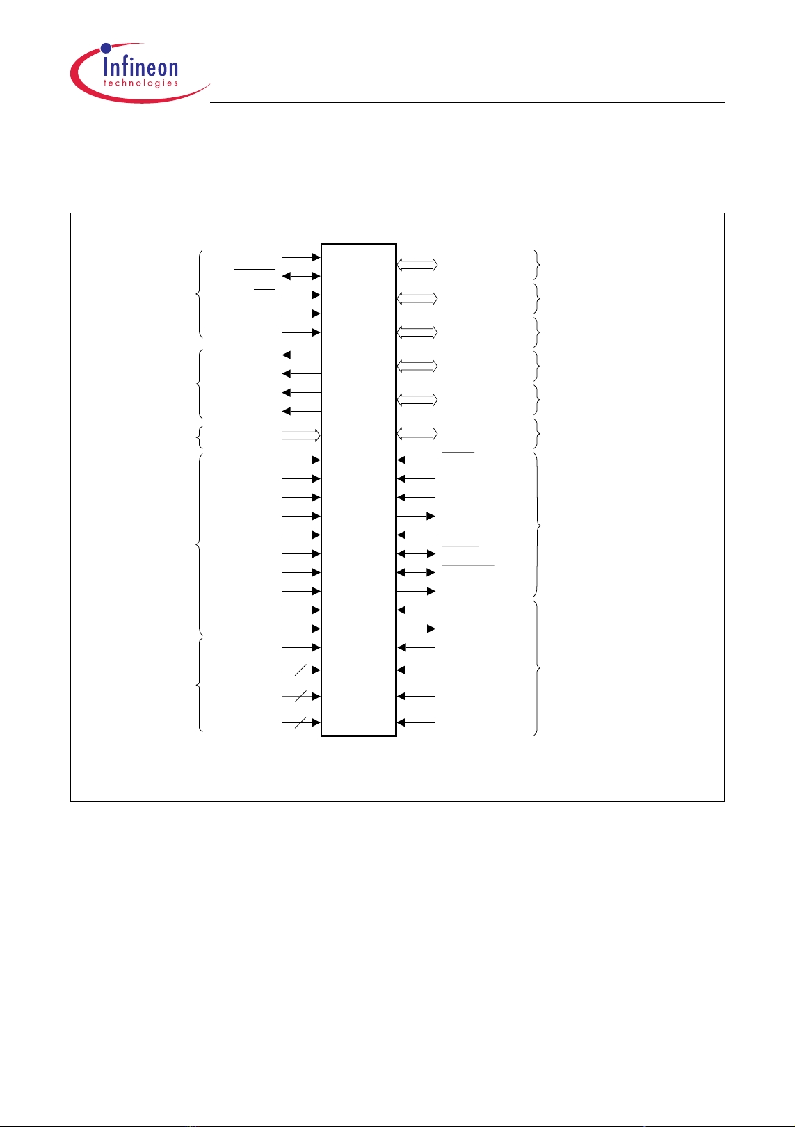
2.2 Logic Symbol
Figure 2-2 shows the TC1161/TC1162 logic symbol.
Gener al Contr ol
PORST
HDRST
NMI
BYPASS
TEST MODE
Por t 0 16- bit
Por t 1 15- bit
Por t 2 14- bit
TC1161/TC1162
General Device InformationAdvance Information
Alter nate Functions
GPTA, SCU
GPTA, ADC
SSC0, MLI0, GPTA, MSC0
MSC0 Contr ol
ADC/ F ADC Anal og
Power Supply
Di gi tal Cir c ui tr y
Power Supply
FCLP0A
FCLN0
SOP0A
SON0
AN[35:0]ADC Analog Inputs
V
DDM
V
SSM
V
DDMF
V
SSMF
V
DDAF
V
SSAF
V
AR EF0
V
AGND0
V
FAREF
V
FAGND
V
DDFL3
V
V
DDP
V
DD
SS
Por t 3 16- bit
Port 4 4- bit
Por t 5 16- bit
ASC0/1, SSC0, SCU, CAN
GPTA, SCU
GPTA, OCDS L2, MLI0
1)
TRST
TC1161/
TC1162
TCK
TDI
TDO
TMS
OCDS / JTAG Control
BRKIN
BRKOUT
T RCLK
XTAL1
XTAL2
V
7
8
9
DDOSC3
V
SSOSC 3
V
DDOSC
V
SSOSC
Oscillator
1) A lternat e f unctions f or CAN m odule is not applic able f or T C1161.
TC1161/TC1162 Logic S ym bol
Figure 2-2 TC1161/TC1162 Logic Symbol
Data Sheet 7 V0.1, 2005-11
2.3 Pin Configuration
Figure 2-3 shows the TC1161/TC1162 pin configuration.
TC1161/TC1162
General Device InformationAdvance Information
Figure 2-3 TC1161/TC1162 Pinning for PG-LQFP-176-2 Package
Data Sheet 8 V0.1, 2005-11

TC1161/TC1162
General Device InformationAdvance Information
2.4 Pad Driver and Input Classes Overview
The TC1161/TC1162 provides different types and classes of input and output lines. For
understanding of the abbreviations in Table 2-2 starting at the next page, Table 2-1
gives an overview on the pad type and class types.
Table 2-1 Pad Driver and Input Classes Overview
Class Power
Supply
A 3.3V LVTTL I/O,
Type Sub Class Speed
Grade
LVTTL
outputs
A1
(e.g. GPIO)
A2
6 MHz No
40 MHz Series termination
(e.g. serial
Termination
recommended
I/Os)
A3
(e.g. BRKIN,
66 MHz/ Yes, series
termination
BRKOUT)
A4
(e.g.Trace Clock)
66 MHz Yes, series
termination
C 3.3V LVDS – 50 MHz Parallel termination
D Analog
–––
input
Data Sheet 9 V0.1, 2005-11

General Device InformationAdvance Information
2.5 Pin Definitions and Functions
Table 2-2 shows the TC1161/TC1162 pin definitions and functions.
Table 2-2 Pin Definitions and Functions
TC1161/TC1162
Symbol Pins I/O Pad
Driver
Class
Parallel Ports
P0 I/O A1
P0.0
P0.1
P0.2
P0.3
P0.4
P0.5
P0.6
P0.7
P0.8
P0.9
P0.10
P0.11
P0.12
P0.13
P0.14
P0.15
145
146
147
148
166
167
173
174
149
150
151
152
168
169
175
176
Power
Supply
V
DDP
Functions
Port 0
Port 0 is a 16-bit bi-directional generalpurpose I/O port which can be alternatively
used for GPTA I/O lines or external trigger
inputs.
IN0 / OUT0 /
IN1 / OUT1 /
IN2 / OUT2 /
IN3 / OUT3 /
IN4 / OUT4 /
IN5 / OUT5 /
IN6 / OUT6 /
REQ2
IN7 / OUT7 /
REQ3
IN8 / OUT8 /
IN9 / OUT9 /
IN10 / OUT10 /
IN11 / OUT11 /
IN12 / OUT12 /
IN13 / OUT13 /
IN14 / OUT14 /
REQ4
IN15 / OUT15 /
REQ5
OUT56 line of GPTA
OUT57 line of GPTA
OUT58 line of GPTA
OUT59 line of GPTA
OUT60 line of GPTA
OUT61 line of GPTA
OUT62 line of GPTA
External trigger input 2
OUT63 line of GPTA
External trigger input 3
OUT64 line of GPTA
OUT65 line of GPTA
OUT66 line of GPTA
OUT67 line of GPTA
OUT68 line of GPTA
OUT69 line of GPTA
OUT70 line of GPTA
External trigger input 4
OUT71 line of GPTA
External trigger input 5
In addition, the state of the port pins are
latched into the software configuration input
register SCU_SCLIR at the rising edge of
HDRST
. Therefore, Port 0 pins can be used
for operating mode selections by software.
Data Sheet 10 V0.1, 2005-11

Table 2-2 Pin Definitions and Functions (cont’d)
TC1161/TC1162
General Device InformationAdvance Information
Symbol Pins I/O Pad
Driver
Power
Supply
Class
P1 I/O V
P1.0
P1.1
P1.2
P1.3
P1.4
P1.5
P1.6
P1.7
P1.8
P1.9
P1.10
P1.11
P1.12
P1.13
P1.14
91
92
93
98
107
108
109
110
94
95
96
97
73
72
71
A1
A1
A1
A1
A1
A1
A1
A1
A2
A2
A2
A2
A1
A1
A1
DDP
Functions
Port 1
Port 1 is a 15-bit bi-directional general
purpose I/O port which can be alternatively
used for GPTA I/O lines and ADC0 interface.
IN16 / OUT16 /
IN17 / OUT17 /
IN18 / OUT18 /
IN19 / OUT19 /
IN20 / OUT20 /
IN21 / OUT21 /
IN22 / OUT22 /
IN23 / OUT23 /
IN24 / OUT24 /
IN25 / OUT25 /
IN26 / OUT26 /
IN27 / OUT27 /
AD0EMUX0
OUT72 line of GPTA
OUT73 line of GPTA
OUT74 line of GPTA
OUT75 line of GPTA
OUT76 line of GPTA
OUT77 line of GPTA
OUT78 line of GPTA
OUT79 line of GPTA
IN48 / OUT48 line of GPTA
IN49 / OUT49 line of GPTA
IN50 / OUT50 line of GPTA
IN51 / OUT51 line of GPTA
ADC0 external multiplexer
control output 0
AD0EMUX1
ADC0 external multiplexer
control output 1
AD0EMUX2
ADC0 external multiplexer
control output 2
In addition, P1.4 also serves as emergency
shut-off input for certain I/O lines (e.g. GPTA
related outputs).
Data Sheet 11 V0.1, 2005-11

Table 2-2 Pin Definitions and Functions (cont’d)
TC1161/TC1162
General Device InformationAdvance Information
Symbol Pins I/O Pad
Driver
Power
Supply
Class
P2 I/O V
P2.0
P2.1
P2.2
P2.3
P2.4
P2.5
P2.6
P2.7
74
75
76
77
78
79
80
81
A2
A2
A2
A2
A1
A2
A1
A1
DDP
Functions
Port 2
Port 2 is a 14-bit bi-directional generalpurpose I/O port which can be alternatively
used for GPTA I/O, and interface for MLI0,
MSC0 or SSC0.
TCLK0A
MLI0 transmit channel clock
output A
IN32 / OUT32
TREADY0A
line of GPTA
MLI0 transmit channel ready
input A
IN33 / OUT33
SLSO03
TVALID0A
line of GPTA
SSC0 slave select output 3
MLI0 transmit channel valid
output A
IN34 / OUT34
TDATA0A
line of GPTA
MLI0 transmit channel data
output A
IN35 / OUT35
RCLK0A
line of GPTA
MLI0 receive channel clock
input A
IN36 / OUT36
RREADY0A
line of GPTA
MLI0 receive channel ready
output A
IN37 / OUT37
RVALID0A
line of GPTA
MLI0 receive channel valid
input A
IN38 / OUT38
RDATA0A
line of GPTA
MLI0 receive channel data
input A
IN39 / OUT39
line of GPTA
Data Sheet 12 V0.1, 2005-11

Table 2-2 Pin Definitions and Functions (cont’d)
TC1161/TC1162
General Device InformationAdvance Information
Symbol Pins I/O Pad
Driver
Class
P2.8
P2.9
P2.10
P2.11
P2.12
P2.13
164
160
161
162
163
165
A2
A2
A2
A2
A2
A1
Power
Supply
Functions
SLSO04
EN00
SLSO05
EN01
FCLP0B
SOP0B
SDI0
SSC0 Slave Select output 4
MSC0 enable output 0
SSC0 Slave Select output 5
MSC0 enable output 1
MSC0 clock output B
MSC0 serial data output B
MSC0 serial data input
Data Sheet 13 V0.1, 2005-11

TC1161/TC1162
General Device InformationAdvance Information
P3 I/O V
P3.0
P3.1
P3.2
P3.3
P3.4
P3.5
P3.6
P3.7
P3.8
P3.9
P3.10
P3.11
P3.12
P3.13
P3.14
P3.15
136
135
129
130
132
126
127
131
128
138
137
144
143
142
134
133
A2
A2
A2
A2
A2
A2
A2
A2
A2
A2
A1
A1
A2
A2
A2
A2
DDP
Port 3
Port 3 is a 16-bit bi-directional generalpurpose I/O port which can be alternatively
1)
used for ASC0/1, SSC0 and CAN
RXD0A
TXD0A
ASC0 receiver inp./outp. A
ASC0 transmitter output A
lines.
This pin is sampled at the rising edge of
PORST
. If this pin and the BYPASS input pin
are both active, then oscillator bypass mode
is entered.
SCLK0
MRST0
SSC0 clock input/output
SSC0 master receive input/
slave transmit output
MTSR0
SSC0 master transmit
output/slave receive input
SLSO00
SLSO01
SLSI0
SLSO02
SLSO06
TXD1A
RXD1A
REQ0
REQ1
RXDCAN0
1)
RXD0B
TXDCAN0
1)
TXD0B
RXDCAN1
1)
RXD1B
TXDCAN1
1)
TXD1B
Data Sheet 14 V0.1, 2005-11

Table 2-2 Pin Definitions and Functions (cont’d)
TC1161/TC1162
General Device InformationAdvance Information
Symbol Pins I/O Pad
Driver
Power
Supply
Functions
Class
P4 I/O V
DDP
Port 4 / Hardware Configuration Inputs
P4.[3:0] HWCFG[3:0] Boot mode and boot location
inputs; inputs are latched
with the rising edge of
HDRST
.
During normal operation, Port 4 pins may be
used as alternate functions for GPTA or
system clock output.
P4.0
P4.1
P4.2
P4.3
86
87
88
90
A1
A1
A2
A2
IN28 / OUT28 /
IN29 / OUT29 /
IN30 / OUT30 /
IN31 / OUT31 /
SYSCLK
IN52 / OUT52 line of GPTA
IN53 / OUT53 line of GPTA
IN54 / OUT54 line of GPTA
IN55 / OUT55 line of GPTA
System Clock Output
Data Sheet 15 V0.1, 2005-11

Table 2-2 Pin Definitions and Functions (cont’d)
TC1161/TC1162
General Device InformationAdvance Information
Symbol Pins I/O Pad
Driver
Power
Supply
Class
P5 I/O A2 V
P5.0
P5.1
P5.2
P5.3
P5.4
P5.5
P5.6
P5.7
1
2
3
4
5
6
7
8
DDP
Functions
Port 5
Port 5 is a 16-bit bi-directional generalpurpose I/O port. In emulation, it is used as a
trace port for OCDS Level 2 debug lines. In
normal operation, it is used for GPTA I/O or
the MLI0 interface.
OCDSDBG0
OCDS L2 Debug Line 0
(Pipeline Status Sig. PS0)
IN40 / OUT40
OCDSDBG1
line of GPTA
OCDS L2 Debug Line 1
(Pipeline Status Sig. PS1)
IN41 / OUT41
OCDSDBG2
line of GPTA
OCDS L2 Debug Line 2
(Pipeline Status Sig. PS2)
IN42 / OUT42
OCDSDBG3
line of GPTA
OCDS L2 Debug Line 3
(Pipeline Status Sig. PS3)
IN43 / OUT43
OCDSDBG4
line of GPTA
OCDS L2 Debug Line 4
(Pipeline Status Sig. PS4)
IN44 / OUT44
OCDSDBG5
line of GPTA
OCDS L2 Debug Line 5
(Break Qualification Line
BRK0)
IN45 / OUT45
OCDSDBG6
line of GPTA
OCDS L2 Debug Line 6
(Break Qualification Line
BRK1)
IN46 / OUT46
OCDSDBG7
line of GPTA
OCDS L2 Debug Line 7
(Break Qualification Line
BRK2)
IN47 / OUT47
line of GPTA
Data Sheet 16 V0.1, 2005-11

Table 2-2 Pin Definitions and Functions (cont’d)
TC1161/TC1162
General Device InformationAdvance Information
Symbol Pins I/O Pad
Driver
Class
P5.8
P5.9
P5.10
P5.11
P5.12
P5.13
P5.14
P5.15
13
14
15
16
17
18
19
20
Power
Supply
Functions
OCDSDBG8
RDATA0B
OCDSDBG9
RVALID0B
OCDSDBG10
RREADY0B
OCDSDBG11
RCLK0B
OCDSDBG12
TDATA0B
OCDSDBG13
TVALID0B
OCDSDBG14
TREADY0B
OCDSDBG15
TCLK0B
OCDS L2 Debug Line 8
(Indirect PC Addr. PC0)
MLI0 receive channel data
input B
OCDS L2 Debug Line 9
(Indirect PC Addr. PC1)
MLI0 receive channel valid
input B
OCDS L2 Debug Line 10
(Indirect PC Addr. PC2)
MLI0 receive channel ready
output B
OCDS L2 Debug Line 11
(Indirect PC Addr. PC3)
MLI0 receive channel clock
input B
OCDS L2 Debug Line 12
(Indirect PC Addr. PC04)
MLI0 transmit channel data
output B
OCDS L2 Debug Line 13
(Indirect PC Addr. PC05)
MLI0 transmit channel valid
output B
OCDS L2 Debug Line 14
(Indirect PC Address PC6)
MLI0 transmit channel ready
input B
OCDS L2 Debug Line 15
(Indirect PC Address PC7)
MLI0 transmit channel clock
output B
Data Sheet 17 V0.1, 2005-11

Table 2-2 Pin Definitions and Functions (cont’d)
TC1161/TC1162
General Device InformationAdvance Information
Symbol Pins I/O Pad
Driver
Class
MSC0 Outputs
C
FCLP0A
FCLN0
SOP0A
SON0
157
156
159
158
O
O
O
O
Power
Supply
V
DDP
Functions
LVDS MSC Clock and Data Outputs
3)
MSC0 Differential Driver Clock Output
Positive A
MSC0 Differential Driver Clock Output
Negative
MSC0 Differential Driver Serial Data Output
Positive A
MSC0 Differential Driver Serial Data Output
Negative
Data Sheet 18 V0.1, 2005-11

Table 2-2 Pin Definitions and Functions (cont’d)
TC1161/TC1162
General Device InformationAdvance Information
Symbol Pins I/O Pad
Driver
Class
Analog Inputs
AN[35:0]
AN0
AN1
AN2
AN3
AN4
AN5
AN6
AN7
AN8
AN9
AN10
AN11
AN12
AN13
AN14
AN15
AN16
AN17
AN18
AN19
AN20
AN21
AN22
AN23
AN24
AN25
AN26
AN27
AN28
AN29
AN30
67
66
65
64
63
62
61
36
60
59
58
57
56
55
50
49
48
47
46
45
44
43
42
41
40
39
38
37
35
34
33
ID – Analog Input Port
Power
Supply
Functions
The Analog Input Port provides altogether 36
analog input lines to ADC0 and FADC.
AN[31:0]: ADC0 analog inputs [31:0]
AN[35:32]: FADC analog differential inputs
Analog input 0
Analog input 1
Analog input 2
Analog input 3
Analog input 4
Analog input 5
Analog input 6
Analog input 7
Analog input 8
Analog input 9
Analog input 10
Analog input 11
Analog input 12
Analog input 13
Analog input 14
Analog input 15
Analog input 16
Analog input 17
Analog input 18
Analog input 19
Analog input 20
Analog input 21
Analog input 22
Analog input 23
Analog input 24
Analog input 25
Analog input 26
Analog input 27
Analog input 28
Analog input 29
Analog input 30
Data Sheet 19 V0.1, 2005-11

Table 2-2 Pin Definitions and Functions (cont’d)
TC1161/TC1162
General Device InformationAdvance Information
Symbol Pins I/O Pad
Driver
Power
Supply
Class
AN31
AN32
AN33
AN34
AN35
32
31
30
29
28
I D – Analog input 31
System I/O
TRST
114 I A2
TCK 115 I A2
TDI 111 I A1
TDO 113 O A2
TMS 112 I A2
BRKIN
BRK
117 I/O A3 V
116 I/O A3 V
2)
2)
2)
V
V
V
V
2)
V
OUT
TRCLK 9OA4 V
NMI 120 I A2
HDRST
PORST
122 I/O A2 V
6)121 I A2
5)
5)
V
V
DDP
DDP
DDP
DDP
DDP
DDP
DDP
DDP
DDP
DDP
DDP
Functions
Analog input 32
Analog input 33
Analog input 34
Analog input 35
JTAG Module Reset/Enable Input
JTAG Module Clock Input
JTAG Module Serial Data Input
JTAG Module Serial Data Output
JTAG Module State Machine Control Input
OCDS Break Input (Alternate Output)
OCDS Break Output (Alternate Input)
Trace Clock for OCDS_L2 Lines
3)4)
3)4)
3)
Non-Maskable Interrupt Input
Hardware Reset Input /
Reset Indication Output
Power-on Reset Input
BYPASS 119 I A1
2)
V
DDP
PLL Clock Bypass Select Input
This input has to be held stable during poweron resets. With BYPASS = 1, the spike filters
in the HDRST
, PORST and NMI inputs are
switched off.
TEST
MODE
118 I A2
5)
V
DDP
Test Mode Select Input
For normal operation of the TC1161/TC1162,
this pin should be connected to high level.
XTAL1
XTAL2
102
103IO
n.a.
V
DDOSC
Oscillator/PLL/Clock Generator
Input/Output Pins
N.C. 21, 89–– – Not Connected
These pins are reserved for future extension
and must not be connected externally.
Data Sheet 20 V0.1, 2005-11

Table 2-2 Pin Definitions and Functions (cont’d)
TC1161/TC1162
General Device InformationAdvance Information
Symbol Pins I/O Pad
Driver
Class
Power Supplies
V
DDM
V
SSM
V
DDMF
V
SSMF
V
DDAF
V
SSAF
V
AREF0
V
AGND0
V
FAREF
V
FAGND
V
DDOSC
54 – – – ADC Analog Part Power Supply (3.3 V)
53 – – – ADC Analog Part Ground for V
24 – – – FADC Analog Part Power Supply (3.3 V)
25 – – – FADC Analog Part Ground for V
23 – – – FADC Analog Part Logic Power Supply
22 – – – FADC Analog Part Logic Ground for V
52 – – – ADC Reference Voltage
51 – – – ADC Reference Ground
26 – – – FADC Reference Voltage
27 – – – FADC Reference Ground
105 – – – Main Oscillator and PLL Power Supply
Power
Supply
Functions
DDM
DDMF
(1.5 V)
DDAF
(1.5 V)
V
DDOSC3
V
SSOSC
V
DDFL3
V
DD
106 – – – Main Oscillator Power Supply (3.3 V)
104 – – – Main Oscillator and PLL Ground
141 – – – Power Supply for Flash (3.3 V)
10,
–– – Core Power Supply (1.5 V)
68,
84,
99,
123,
153,
170
Data Sheet 21 V0.1, 2005-11

Table 2-2 Pin Definitions and Functions (cont’d)
TC1161/TC1162
General Device InformationAdvance Information
Symbol Pins I/O Pad
Driver
Power
Supply
Functions
Class
V
DDP
11,
–– – Port Power Supply (3.3 V)
69,
83,
100,
124,
154,
171,
139
V
SS
12,
–– – Ground
70,
85,
101,
125,
155,
172,
140,
82
1) Not applicable to TC1161
2) These pads are I/O pads with input only function. Its input characteristics are identical with the input
characteristics as defined for class A pads.
3) In case of a power-fail condition (one or more power supply voltages drop below the specified voltage range),
an undefined output driving level may occur at these pins.
4) Programmed by software as either break input or break output.
5) These pads are input only pads with input characteristics.
6) The dual input reset system of TC1161/TC1162 assumes that the PORST
only.
reset pin is used for power on reset
Data Sheet 22 V0.1, 2005-11

TC1161/TC1162
General Device InformationAdvance Information
Table 2-3 List of Pull-up/Pull-down Reset Behavior of the Pins
Pins PORST
=0 PORST=1
TDI, TMS, TDO Pull-up
HDRST
Drive-low Pull-up
BYPASS Pull-up High-impedance
TRST
, TCK High-impedance Pull-down
TRCLK High-impedance
BRKIN
NMI
, BRKOUT, TESTMODE Pull-up
, PORST Pull-down
Data Sheet 23 V0.1, 2005-11

TC1161/TC1162
Functional DescriptionAdvance Information
3 Functional Description
Chapter 3 provides an overview of the TC1161/TC1162 functional description.
3.1 System Architecture and On-Chip Bus Systems
The TC1161/TC1162 has two independent on-chip buses (see also TC1161/TC1162
block diagram on Page 2-6):
• Local Memory Bus (LMB)
• System Peripheral Bus (SPB)
The LMB Bus connects the CPU local resources for data and instruction fetch. The Local
Memory Bus interconnects the memory units and functional units, such as CPU and
PMU. The main target of the LMB bus is to support devices with fast response times,
optimized for speed. This allows the DMI and PMI fast access to local memory and
reduces load on the FPI bus. The Tricore system itself is located on LMB bus.
The Local Memory Bus is a synchronous, pipelined, split bus with variable block size
transfer support. It supports 8-, 16-, 32- and 64-bit single transactions and variable
length 64-bit block transfers.
The SPB Bus is accessible to the CPU via the LMB Bus bridge. The System Peripheral
Bus (SPB Bus) in TC1161/TC1162 is an on-chip FPI Bus. The FPI Bus interconnects the
functional units of the TC1161/TC1162, such as the DMA and on-chip peripheral
components. The FPI Bus is designed to be quick to be acquired by on-chip functional
units, and quick to transfer data. The low setup overhead of the FPI Bus access protocol
guarantees fast FPI Bus acquisition, which is required for time-critical applications.The
FPI Bus is designed to sustain high transfer rates. For example, a peak transfer rate of
up to 264 Mbyte/s can be achieved with a 66 MHz bus clock and 32-bit data bus. Multiple
data transfers per bus arbitration cycle allow the FPI Bus to operate at close to its peak
bandwidth.
Both the LMB Bus and the SPB Bus runs at full CPU speed. The maximum CPU speed
is 66 MHz.
Additionally, two simplified bus interfaces are connected to and controlled by the DMA
Controller.
•DMA Bus
• SMIF Interface.
Data Sheet 24 V0.1, 2005-11

TC1161/TC1162
Functional DescriptionAdvance Information
3.2 On-Chip Memories
As shown in the TC1161/TC1162 block diagram on Page 2-6, some of the
TC1161/TC1162 units provide on-chip memories that are used as program or data
memory.
• Program memory in PMU
– 16 Kbyte Boot ROM (BROM)
– 1024 Kbyte Program Flash (PFlash)
• Program memory in PMI
– 8 Kbyte Scratch-Pad RAM (SPRAM)
– 8 Kbyte Instruction Cache (ICACHE)
• Data memory in PMU
– 16 Kbyte Data Flash (DFlash)
– 4 Kbyte Overlay RAM (OVRAM)
• Data memory in DMI
– 32 Kbyte Local Data RAM (LDRAM)
• On-chip SRAM with parity error protection
Features of Program Flash
• 1024 Kbyte on-chip program Flash memory
• Usable for instruction code or constant data storage
• 256-byte program interface
– 256 bytes are programmed into PFLASH page in one step/command
• 256-bit read interface
– Transfer from PFLASH to CPU/PMI by four 64-bit single cycle burst transfers
• Dynamic correction of single-bit errors during read access
• Detection of double-bit errors
• Fixed sector architecture
– Eight 16 Kbyte, one 128 Kbyte, one 256 Kbyte and one 512 Kbyte sectors
– Each sector separately erasable
– Each sector separately write-protectable
• Configurable read protection for complete PFLASH with sophisticated read access
supervision, combined with write protection for complete PFLASH (protection against
“Trojan horse” software)
• Configurable write protection for each sector
– Each sector separately write-protectable
– With capability to be re-programmed
– With capability to be locked forever (OTP)
• Password mechanism for temporary disabling of write and read protection
• On-chip generation of programming voltage
• JEDEC-standard based command sequences for PFLASH control
– Write state machine controls programming and erase operations
– Status and error reporting by status flags and interrupt
Data Sheet 25 V0.1, 2005-11

TC1161/TC1162
Functional DescriptionAdvance Information
• Margin check for detection of problematic PFLASH bits
Features of Data Flash
• 16 Kbyte on-chip data Flash memory, organized in two 8 Kbyte banks
• Usable for data storage with EEPROM functionality
• 128 Byte of program interface
– 128 bytes are programmed into one DFLASH page by one step/command
• 64-bit read interface (no burst transfers)
• Dynamic correction of single-bit errors during read access
• Detection of double-bit errors
• Fixed sector architecture
– Two 8 Kbyte banks/sectors
– Each sector separately erasable
• Configurable read protection (combined with write protection) for complete DFLASH
together with PFLASH read protection
• Password mechanism for temporary disabling of write and read protection
• Erasing/programming of one bank possible while reading data from the other bank
• Programming of one bank while erasing the other bank possible
• On-chip generation of programming voltage
• JEDEC-standard based command sequences for DFLASH control
– Write state machine controls programming and erase operations
– Status and error reporting by status flags and interrupt
• Margin check for detection of problematic DFLASH bits
Data Sheet 26 V0.1, 2005-11

TC1161/TC1162
Functional DescriptionAdvance Information
3.3 Memory Maps
This chapter gives an overview of the TC1161/TC1162 memory map and describes the
address locations and access possibilities for the units, memories, and reserved areas
as “seen” from different on-chip buses’ (SPB and LMB) point of view.
3.3.1 Architectural Address Map
Table 3-1 shows the overall architectural address map as defined for the TriCore and as
implemented in TC1161/TC1162.
Table 3-1 TC1161/TC1162 Architectural Address Map
Segment
0-7 Global 8 x 256
8 Global
9 Global
10 Global
11 Global
12 Local LMB
13 DMI 64 Mbyte Local Data Memory RAM; non-cached
Contents Size Description
Reserved (MMU space); cached
Mbyte
256 Mbyte Reserved (246 Mbyte); PMU, Boot ROM;
Memory
256 Mbyte FPI space; cached
Memory
256 Mbyte Reserved (246 Mbyte), PMU, Boot ROM; non-
Memory
256 Mbyte FPI space; non-cached
Memory
256 Mbyte Reserved; bottom 4 Mbyte visible from FPI bus
Memory
PMI 64 Mbyte Local Code Memory RAM; non-cached
EXT_PER 96 Mbyte Reserved; non-cached
cached
cached
in segment 14; cached
EXT_EMU 16 Mbyte Reserved; non-cached
BOOTROM 16 Mbyte Boot ROM space, Boot ROM mirror;
non-cached
Data Sheet 27 V0.1, 2005-11

Functional DescriptionAdvance Information
Table 3-1 TC1161/TC1162 Architectural Address Map (cont’d)
TC1161/TC1162
Seg-
Contents Size Description
ment
14 EXTPER 128 Mbyte Reserved;
non-speculative; non-cached; no execution
CPU[0 ..15]
image region
15 LMB_PER
CSFRs
INT_PER
16 x 8
Mbyte
256
Mbyte
Non-speculative; non-cached; no execution
CSFRs of CPUs[0 ..15];
LMB & FPI Peripheral Space;
non-speculative; non-cached;
no execution
Data Sheet 28 V0.1, 2005-11

TC1161/TC1162
Functional DescriptionAdvance Information
3.3.2 How to Read the Address Maps
The bus-specific address maps describe how the different bus master devices react on
accesses to on-chip memories and modules, and which address ranges are valid or
invalid for the corresponding buses.
The FPI Bus address map shows the system addresses from the point of view of the
SPB master agents. SPB master agents are OCDS and DMA.
The LMB address map shows the system addresses from the point of view of the LMB
master agents. LMB master agents are PMI and DMI.
Table 3-2 defines the acronyms and other terms that are used in the address maps
(Table 3-3 to Table 3-5).
Table 3-2 Definition of Acronyms and Terms
Term Description
…BE Means “Bus error” generation.
…BET Means “Bus error & trap” generation.
SPBBE A bus access is terminated with a bus error on the SPB.
SPBBET A bus access is terminated with a bus error on the SPB and a DSE
trap (read access) or DAE trap (write access).
LMBBE A bus access is terminated with a bus error on the LMB.
LMBBET A bus access is terminated with a bus error on the LMB and a DSE
trap (read access) or DAE trap (write access).
access A bus access is allowed and is executed.
ignore A bus access is ignored and is not executed. No bus error is
generated.
trap A DSE trap (read access) or DAE trap (write access) is generated.
32 Only 32-bit word bus accesses are permitted to that
register/address range.
nE A bus access generates no bus error, although the bus access
points to an undefined address or address range. This is valid e.g.
for CPU accesses (MTCR/MFCR) to undefined addresses in the
CSFR range.
Data Sheet 29 V0.1, 2005-11

TC1161/TC1162
Functional DescriptionAdvance Information
3.3.3 Contents of the Segments
This section summarizes the contents of the segments.
Segments 0-7
These segments are reserved segments in the TC1161/TC1162.
Segment 8
From the SPB point of view (DMA and Cerberus), this memory segment allows accesses
to all PMU memories (PFLASH, DFLASH, BROM, and TROM).
From the CPU point of view (PMI and DMI), this memory segment allows cached
accesses to all PMU memories (PFLASH, DFLASH, BROM, and TROM).
Segment 9
This memory segment is reserved in the TC1161/TC1162.
Segment 10
From the SPB point of view (DMA and Cerberus), this memory segment allows accesses
to all PMU memories (PFLASH, DFLASH, BROM, and TROM).
From the CPU point of view (PMI and DMI), this memory segment allows non-cached
accesses to all PMU memories (PFLASH, DFLASH, BROM, and TROM).
Segment 11
This memory segment is reserved in the TC1161/TC1162.
Segment 12
From the SPB point of view (PCP, DMA, and Cerberus), this memory segment is
reserved in the TC1161/TC1162.
From the CPU point of view (PMI and DMI), this memory segment allows cached
accesses to the PMU memory, OVRAM.
Segment 13
From the SPB point of view (DMA and Cerberus), this memory segment is reserved in
the TC1161/TC1162.
From the CPU point of view (PMI and DMI), this memory segment allows non-cached
accesses to the PMI scratch-pad RAM, read access to the boot ROM and test ROM
(BROM and TROM) and the DMI memories (LDRAM).
Data Sheet 30 V0.1, 2005-11

TC1161/TC1162
Functional DescriptionAdvance Information
Segment 14
From the SPB point of view (DMA and Cerberus), this memory segment allows accesses
to the PMU Overlay memory (OVRAM), the DMI Local Data RAM (LDRAM), and the PMI
scratch-pad RAM (SPRAM).
From the CPU point of view (PMI and DMI), this memory segment is reserved in the
TC1161/TC1162.
Segment 15
From the SPB point of view (DMA and Cerberus), this memory segment allows accesses
to all SFRs and CSFRs, and the MLI transfer windows.
From the CPU point of view (PMI and DMI), this memory segment allows accesses to all
SFRs and CSFRs, and the MLI transfer windows.
Data Sheet 31 V0.1, 2005-11

TC1161/TC1162
Functional DescriptionAdvance Information
3.3.4 Address Map of the FPI Bus System
Table 3-3 and Table 3-4 shows the address maps of the FPI Bus System.
3.3.4.1 Segments 0 to 14
Table 3-3 shows the address maps of segments 0 to 14 as it is seen from the SPB bus
masters, DMA and OCDS.
Table 3-3 SPB Address Map of Segment 0 to 14
Segment
Address
Range
0-7 0000 0000
0000 0007
0000 0008
7FFF FFFF
Size Description Access Type
Read Write
-
H
H
H
8 byte Reserved (virtual address
space)
-
8 × 256
Mbyte
H
MPN trap MPN trap
SPBBE SPBBE
Data Sheet 32 V0.1, 2005-11

Table 3-3 SPB Address Map of Segment 0 to 14 (cont’d)
TC1161/TC1162
Functional DescriptionAdvance Information
Segment
Address
Range
8 8000 0000H -
800F FFFF
H
8010 0000H 8017 7FFF
H
8017 8000H 807F FFFF
8080 0000
8FDF FFFF
8FE0 0000
8FE0 1FFF
H
-
H
H
-
H
H
8FE0 2000H 8FE0 3FFF
H
8FE0 4000H 8FE0 FFFF
8FE1 0000
8FE1 1FFF
H
-
H
H
8FE1 2000H 8FE1 3FFF
H
8FE1 4000H 8FF1 FFFF
8FF2 0000
8FF5 FFFF
8FF6 0000
8FFF BFFF
8FFF C000
8FFF FFFF
9 9000 0000
9FFF FFFF
H
-
H
H
-
H
H
H
H
-
H
H
Size Description Access Type
Read Write
1 Mbyte Program Flash (PFLASH) access access
≈ 0.5
Reserved access
2)
Mbyte
6.5 Mbyte Reserved LMBBE &
SPBBE
246
Mbyte
8 Kbyte Data Flash (DFLASH)
Reserved LMBBE &
SPBBE
access access
Bank 0
8 Kbyte Reserved access
2)
48 Kbyte Reserved LMBBE &
SPBBE
8 Kbyte Data Flash (DFLASH)
access access
Bank 1
8 Kbyte Reserved access
2)
1 Mbyte Reserved LMBBE &
SPBBE
256
Reserved
Kbyte
624
Reserved
Kbyte
-
16 Kbyte Boot ROM (BROM) access
256
Reserved SPBBE SPBBE
Mbyte
access
LMBBE
LMBBE
access
LMBBE
access
LMBBE
1)
1)2)
1)
1)2)
1)
1)2)
Data Sheet 33 V0.1, 2005-11

Table 3-3 SPB Address Map of Segment 0 to 14 (cont’d)
TC1161/TC1162
Functional DescriptionAdvance Information
Segment
Address
Range
10 A000 0000H -
A00F FFFF
H
A010 0000H A017 FFFF
H
A017 8000H A07F FFFF
A080 0000
AFDF FFFF
AFE0 0000
AFE0 1FFF
H
-
H
H
-
H
H
AFE0 2000H AFE0 3FFF
H
AFE0 4000H AFE0 FFFF
AFE1 0000
AFE1 1FFF
H
-
H
H
AFE1 2000H AFE1 3FFF
H
AFE1 4000H AFF1 FFFF
AFF2 0000
AFF5 FFFF
AFF6 0000
AFFF BFFF
AFFF C000
AFFF FFFF
11 B000 0000
BFFF FFFF
12 C000 0000
C000 0FFF
C000 1000
CFFF FFFF
H
-
H
H
-
H
H
H
H
-
H
H
-
H
H
-
H
H
Size Description Access Type
Read Write
1 Mbyte Program Flash (PFLASH) access access
≈ 0.5
Reserved access
2)
Mbyte
6.5 Mbyte Reserved LMBBE &
SPBBE
246
Mbyte
8 Kbyte Data Flash (DFLASH)
Reserved LMBBE &
SPBBE
access access
Bank 0
8 Kbyte Reserved access
2)
48 Kbyte Reserved LMBBE &
SPBBE
8 Kbyte Data Flash (DFLASH)
access access
Bank 1
8 Kbyte Reserved access
2)
1 Mbyte Reserved LMBBE &
SPBBE
256
Reserved
Kbyte
624
Reserved
Kbyte
-
16 Kbyte Boot ROM (BROM) access
256
Reserved SPBBE SPBBE
Mbyte
4 Kbyte Overlay memory
SPBBE SPBBE
(OVRAM)
≈ 256
Reserved SPBBE SPBBE
Mbyte
access
LMBBE
LMBBE
access
LMBBE
access
ignore
1)
1)2)
1)
1)2)
1)
1)2)
Data Sheet 34 V0.1, 2005-11

Table 3-3 SPB Address Map of Segment 0 to 14 (cont’d)
TC1161/TC1162
Functional DescriptionAdvance Information
Segment
Address
Range
13 D000 0000H -
D000 7FFF
D000 8000
D3FF FFFF
D400 0000
D400 1FFF
D400 2000
D7FF FFFF
D800 0000
DEFF FFFF
DF00 0000
DFFF FFEF
DFFF FFF0
DFFF FFFF
H
-
H
H
-
H
H
-
H
H
-
H
H
-
H
H
H
H
Size Description Access Type
Read Write
32 Kbyte DMI Local Data RAM
SPBBE SPBBE
(LDRAM)
≈ 64
Reserved SPBBE SPBBE
Mbyte
8 Kbyte PMI Scratch-Pad RAM
SPBBE SPBBE
(SPRAM)
≈ 64
Reserved SPBBE SPBBE
Mbyte
112
Reserved SPBBE SPBBE
Mbyte
≈ 16
Reserved (for Boot Rom) SPBBE SPBBE
Mbyte
-
16 byte microROM SPBBE SPBBE
Data Sheet 35 V0.1, 2005-11

Table 3-3 SPB Address Map of Segment 0 to 14 (cont’d)
TC1161/TC1162
Functional DescriptionAdvance Information
Segment
14 E000 0000H -
15 F000 0000
1) Only applicable when writing Flash command sequences.
2) Read and write accesses to this address range will not generate any traps.
Address
Range
E7FF FFFF
E800 0000
E800 0FFF
E800 1000
E800 1FFF
H
-
H
H
-
H
H
E800 2000H E83F FFFF
E840 0000
E840 7FFF
E840 8000
E840 DFFF
H
-
H
H
-
H
H
E840 E000H E84F FFFF
E850 0000
E850 1FFF
E850 2000
E850 3FFF
H
-
H
H
-
H
H
E850 4000H E85F FFFF
E860 C000
EFFF FFFF
FFFF FFFF
H
-
H
H
-
H
H
Size Description Access Type
128 MB Reserved LMBBE LMBBE
4 Kbyte Overlay memory
(OVRAM)
4 Kbyte Reserved access
≈ 4
Reserved LMBBE LMBBE
Mbyte
32 Kbyte DMI Local Data RAM
(LDRAM)
24 Kbyte Reserved access
≈ 1 Mbyte Reserved LMBBE LMBBE
8 Kbyte PMI Scratch-Pad RAM
(SPRAM)
8 Kbyte Reserved access
≈ 1 Mbyte Reserved LMBBE LMBBE
≈ 122
Reserved LMBBE LMBBE
Mbyte
256
see Table 3-4
Mbyte
Read Write
access access
2)
access
access access
2)
access
access access
2)
access
2)
2)
2)
Data Sheet 36 V0.1, 2005-11

TC1161/TC1162
Functional DescriptionAdvance Information
3.3.4.2 Segment 15
Table 3-4 shows the address map of segment 15 as seen from the SPB bus masters
DMA and OCDS. Please note that access in Table 3-4 means only that an access to an
address within the defined address range is not automatically incorrect or ignored. If an
access is really addressing a correct address, it can be found in the detailed tables in the
TC116x User’s Manual, Register Overview’s chapter.
Table 3-4 SPB Address Map of Segment 15
Unit Address
Range
System Control Unit (SCU) and
Watchdog Timer (WDT)
System Peripheral Bus Control Unit
(SBCU)
F000 0000
F000 00FF
F000 0100
F000 01FF
System Timer (STM) F000 0200
F000 02FF
Reserved F000 0300
F000 03FF
On-Chip Debug Support (Cerberus) F000 0400
F000 04FF
Reserved F000 0500
F000 07FF
MicroSecond Bus Controller 0
(MSC0)
F000 0800
F000 08FF
Reserved F000 0900
F000 09FF
Async./Sync. Serial Interface 0
(ASC0)
Async./Sync. Serial Interface 1
(ASC1)
F000 0A00
F000 0AFF
F000 0B00
F000 0BFF
Port 0 F000 0C00
F000 0CFF
Port 1 F000 0D00
F000 0DFF
Port 2 F000 0E00
F000 0EFF
Size Access Type
Read Write
-
256
H
byte
H
-
256
H
byte
H
-
256
H
byte
H
-
– SPBBE SPBBE
H
H
-
256
H
byte
H
-
– SPBBE SPBBE
H
H
-
256
H
byte
H
-
– SPBBE SPBBE
H
H
-
256
H
byte
H
-
256
H
byte
H
-
256
H
byte
H
-
256
H
byte
H
-
256
H
byte
H
access access
access access
access access
access access
access access
access access
access access
access access
access access
access access
Data Sheet 37 V0.1, 2005-11

Table 3-4 SPB Address Map of Segment 15 (cont’d)
TC1161/TC1162
Functional DescriptionAdvance Information
Unit Address
Range
Port 3 F000 0F00H -
F000 0FFF
Port 4 F000 1000
F000 10FF
Port 5 F000 1100
F000 11FF
Reserved F000 1200
F000 12FF
Reserved F000 1300
F000 13FF
Reserved F000 1400
F000 14FF
Reserved F000 1500
F000 15FF
Reserved F000 1600
F000 16FF
Reserved F000 1700
F000 17FF
General Purpose Timer Array 0
(GPTA0)
F000 1800
F000 1FFF
Reserved F000 2000
F000 27FF
Reserved F000 2800
F000 2FFF
Reserved F000 3000
F000 3BFF
Direct Memory Access Controller
(DMA)
F000 3C00
F000 3EFF
Reserved F000 3F00
F000 3FFF
MultiCAN Controller (CAN) F000 4000
F000 5FFF
H
-
H
H
-
H
H
-
H
H
-
H
H
-
H
H
-
H
H
-
H
H
-
H
H
-
H
H
-
H
H
-
H
H
-
H
H
-
H
H
-
H
H
-
H
H
Size Access Type
Read Write
256
access access
byte
256
access access
byte
256
access access
byte
– SPBBE SPBBE
– SPBBE SPBBE
– SPBBE SPBBE
– SPBBE SPBBE
– SPBBE SPBBE
– SPBBE SPBBE
8 × 256
access access
byte
– SPBBE SPBBE
– SPBBE SPBBE
– SPBBE SPBBE
3 × 256
access access
byte
– SPBBE SPBBE
8 Kbyte access
1)
access
1)
Data Sheet 38 V0.1, 2005-11

Table 3-4 SPB Address Map of Segment 15 (cont’d)
TC1161/TC1162
Functional DescriptionAdvance Information
Unit Address
Range
Reserved F000 6000H -
F003 FFFF
Reserved F004 0000
F004 3EFF
Reserved F004 3F00
F004 3FFF
H
-
H
H
-
H
H
Reserved F004 4000H -
F004 FFFF
Reserved F005 0000
F005 1FFF
H
-
H
H
Reserved F005 2000H -
F005 FFFF
Reserved F006 0000
F006 2FFF
H
-
H
H
Reserved F006 3000H -
F007 FFFF
Reserved F008 0000
F00F FFFF
Reserved F010 0000
F010 00FF
Synchronous Serial Interface 0
(SSC0)
F010 0100
F010 01FF
Reserved F010 0200
F010 02FF
Fast Analog-to-Digital Converter
(FADC)
Analog-to-Digital Converter 0
(ADC0)
F010 0300H F010 03FF
F010 0400
F010 05FF
Reserved F010 0600
F010 07FF
Reserved F010 0800
F010 9FFF
H
-
H
H
-
H
H
-
H
H
-
H
H
H
-
H
H
-
H
H
-
H
H
Size Access Type
Read Write
– SPBBE SPBBE
– SPBBE SPBBE
256
access
2)
access
byte
– SPBBE SPBBE
8 Kbyte nE, 32
3)
nE, 32
– SPBBE SPBBE
12
nE, 32
3)
nE, 32
Kbyte
– SPBBE SPBBE
– SPBBE SPBBE
– SPBBE SPBBE
256
access access
byte
256
access
2)
access
byte
256
access access
byte
2 × 256
access access
byte
– SPBBE SPBBE
– SPBBE SPBBE
2)
3)
3)
2)
Data Sheet 39 V0.1, 2005-11

Table 3-4 SPB Address Map of Segment 15 (cont’d)
TC1161/TC1162
Functional DescriptionAdvance Information
Unit Address
Range
Reserved F010 A000H -
F010 BFFF
Micro Link Interface 0 (MLI0) F010 C000
F010 C0FF
Reserved F010 C100
F010 C1FF
H
-
H
H
-
H
H
Memory Checker (MCHK) F010 C200H -
F010 C2FF
Reserved F010 C300
F01D FFFF
MLI0 Small Transfer Windows F01E 0000
F01E 7FFF
Reserved F01E 8000
F01E FFFF
H
-
H
H
-
H
H
-
H
H
Reserved F01F 0000H -
F01F FFFF
MLI0 Large Transfer Windows F020 0000
F023FFFF
Reserved F024 0000
F027 FFFF
H
-
H
H
-
H
H
Reserved F028 0000H -
F7E0 FEFF
CPU CPU Slave Interface
Registers (CPS)
F7E0 FF00
F7E0 FFFF
CPU Core SFRs & GPRs F7E1 0000
F7E1 FFFF
Reserved F7E2 0000
F7FF FFFF
Reserved F800 0000
F800 03FF
Reserved F800 0400
F800 04FF
H
-
H
H
-
H
H
-
H
H
-
H
H
-
H
H
Size Access Type
Read Write
– SPBBE SPBBE
256
access access
byte
256
access
2)
access
byte
256
access access
byte
– SPBBE SPBBE
4 × 8
access access
Kbyte
4 × 8
access
2)
access
Kbyte
– SPBBE SPBBE
4 × 64
access access
Kbyte
4 × 64
access
2)
access
Kbyte
– SPBBE SPBBE
256
access access
byte
64
access access
Kbyte
– SPBBE SPBBE
– SPBBE SPBBE
– LMBBE &
LMBBE
SPBBE
2)
2)
2)
Data Sheet 40 V0.1, 2005-11

Table 3-4 SPB Address Map of Segment 15 (cont’d)
TC1161/TC1162
Functional DescriptionAdvance Information
Unit Address
Range
Program Memory Unit (PMU) F800 0500H -
F800 05FF
Reserved F800 0600
F800 0FFF
Flash Register F800 1000
F800 23FF
Reserved F800 2400
F801 00FF
Reserved F801 0100
F801 01FF
Reserved F801 0200
F87F F9FF
Reserved F87F FA00
F87F FAFF
Reserved F87F FB00
F87F FBFF
CPU DMI Registers F87F FC00
F87F FCFF
PMI Registers F87F FD00
F87F FDFF
Local Memory Bus Control Unit
(LBCU)
F87F FE00
F87F FEFF
LFI Bridge F87F FF00
F87F FFFF
Reserved F880 0000
FFFF FFFF
1) For TC1161, read and write accesses to this address range will not generate any traps.
2) Read and write accesses to this address range will not generate any traps.
3) For “32” access type, read and write accesses to this address range will not generate any traps.
Size Access Type
Read Write
256
byte
H
-
– LMBBE &
H
H
-
5 Kbyte access access
H
H
-
– LMBBE &
H
H
-
– LMBBE &
H
H
-
– LMBBE &
H
H
-
– LMBBE &
H
H
-
– LMBBE &
H
H
-
256
H
byte
H
-
256
H
byte
H
-
256
H
byte
H
-
256
H
byte
H
-
– LMBBE &
H
H
access access
SPBBE
SPBBE
SPBBE
SPBBE
SPBBE
SPBBE
access access
access access
access access
access access
SPBBE
LMBBE
LMBBE
LMBBE
LMBBE
LMBBE
LMBBE
LMBBE
Data Sheet 41 V0.1, 2005-11

TC1161/TC1162
Functional DescriptionAdvance Information
3.3.5 Address Map of the Local Memory Bus (LMB)
Table 3-5 shows the address map as seen from the LMB bus masters (PMI and DMI).
Table 3-5 LMB Address Map
Segment
1)
0-7
1)
8
Address
Range
0000 0000H 0000 0007
0000 0008
7FFF FFFF
H
-
H
H
8000 0000H 800F FFFF
H
8010 0000H 8017 7FFF
H
8017 8000H 807F FFFF
8080 0000
8FDF FFFF
8FE0 0000
8FE0 1FFF
H
-
H
H
-
H
H
8FE0 2000H 8FE0 3FFF
H
8FE0 4000H 8FE0 FFFF
8FE1 0000
8FE1 1FFF
H
-
H
H
8FE1 2000H 8FE1 3FFF
H
8FE1 4000H 8FF1 FFFF
8FF2 0000
8FF5 FFFF
8FF6 0000
8FFF BFFF
8FFF C000
8FFF FFFF
H
-
H
H
-
H
H
-
H
H
Size Description Action
Read Write
8 byte Reserved (virtual address
MPN trap MPN trap
space)
8 × 256
SPBBET SPBBE
Mbyte
1 Mbyte Program Flash (PFLASH) access access
≈ 0.5
Reserved access
3)
access
2)
2)3)
Mbyte
6.5 Mbyte Reserved LMBBET LMBBET
246
Reserved LMBBET LMBBET
Mbyte
8 Kbyte Data Flash (DFLASH)
access access
2)
Bank 0
8 Kbyte Reserved access
3)
access
2)3)
48 Kbyte Reserved LMBBET LMBBET
8 Kbyte Data Flash (DFLASH)
access access
2)
Bank 1
8 Kbyte Reserved access
3)
access
2)3)
1 Mbyte Reserved LMBBET LMBBET
256 Kbyte Reserved
624 Kbyte Reserved
16 Kbyte Boot ROM (BROM) access
Data Sheet 42 V0.1, 2005-11

Table 3-5 LMB Address Map (cont’d)
TC1161/TC1162
Functional DescriptionAdvance Information
Segment
1)
9
4)
10
4)
11
Address
Range
9000 0000H 9FFF FFFF
H
A000 0000H A00F FFFF
H
A010 0000H A017 FFFF
H
A017 8000H A07F FFFF
A080 0000
AFDF FFFF
AFE0 0000
AFE0 1FFF
H
-
H
H
-
H
H
AFE0 2000H AFE0 3FFF
H
AFE0 4000H AFE0 FFFF
AFE1 0000
AFE1 1FFF
H
-
H
H
AFE1 2000H AFE1 3FFF
H
AFE1 4000H AFF1 FFFF
AFF2 0000
AFF5 FFFF
AFF6 0000
AFFF BFFF
AFFF C000
AFFF FFFF
H
-
H
H
-
H
H
-
H
H
B000 0000H BFFF FFFF
H
Size Description Action
Read Write
256
Reserved SPBBET SPBBE
Mbyte
1 Mbyte Program Flash (PFLASH) access access
≈ 0.5
Reserved access
3)
access
2)
2)3)
Mbyte
6.5 Mbyte Reserved LMBBET LMBBET
246
Reserved LMBBET LMBBET
Mbyte
8 Kbyte Data Flash (DFLASH)
access access
2)
Bank 0
8 Kbyte Reserved access
3)
access
2)3)
48 Kbyte Reserved LMBBET LMBBET
8 Kbyte Data Flash (DFLASH)
access access
2)
Bank 1
8 Kbyte Reserved access
3)
access
2)3)
1 Mbyte Reserved LMBBET LMBBET
256 Kbyte Reserved
624 Kbyte Reserved
16 Kbyte Boot ROM (BROM) access
256
Reserved SPBBET SPBBE
Mbyte
Data Sheet 43 V0.1, 2005-11

Table 3-5 LMB Address Map (cont’d)
TC1161/TC1162
Functional DescriptionAdvance Information
Segment
1)
12
4)
13
4)
14
Address
Range
C000 0000H C000 0FFF
C000 1000
H
C000 1FFF
C000 2000H CFFF FFFF
D000 0000H D000 7FFF
D000 8000
H
D000 DFFF
D000 E000H D3FF FFFF
D400 0000
H
D400 1FFF
D400 2000
H
D400 3FFF
D400 4000H D7FF FFFF
D800 0000
H
DEFF FFFF
DF00 0000
H
DFFF FFEF
E000 0000H E7FF FFFF
E800 0000
EFFF FFFF
-
H
H
Size Description Action
Read Write
4 Kbyte Overlay memory
H
-
4 Kbyte Reserved access
H
256
Mbyte
H
(OVRAM)
Reserved LMBBET LMBBET
32 Kbyte DMI Local Data RAM
H
-
24 Kbyte Reserved access
H
(LDRAM)
access access
3)
access
SPBBE
SPBBE
5)
64 Mbyte Reserved LMBBET LMBBET
H
-
8 Kbyte PMI Scratch-Pad RAM
H
-
8 Kbyte Reserved access
H
≈ 64
Mbyte
H
-
112
Mbyte
H
-
16 Mbyte Reserved (for Boot Rom)
H
128
Mbyte
H
128
(SPRAM)
Reserved LMBBET LMBBET
Reserved
Reserved LMBBET LMBBET
Reserved LMBBET LMBBET
access access
3)
Mbyte
access
access
SPBBE
access
SPBBE
access
3)
5)
3)
Data Sheet 44 V0.1, 2005-11

Table 3-5 LMB Address Map (cont’d)
TC1161/TC1162
Functional DescriptionAdvance Information
Segment
15 F000 0000H -
Address
Range
F7FF FFFF
Size Description Action
Read Write
H
128
Mbyte
Address map is identical
to FPI Bus segment 15
SPBBET SPBBE
address map (see
Table 3-5)
Reserved areas give an
bus error.
-
F800 0000
F800 03FF
F800 0400
F800 04FF
F800 0500
F800 05FF
F800 0600
F800 0FFF
F800 1000
F800 23FF
F800 2400
F87F FBFF
F87F FC00
F87F FCFF
F87F FD00
F87F FDFF
F87F FE00
F87F FEFF
F87F FF00
F87F FFFF
F880 0000
FFFF FFFF
1) Cached area
2) Only applicable when writing Flash command sequences
3) Read and write accesses to this address range will not generate any traps.
4) Non-cached area
5) If accessible, read and write accesses to this address range will not generate any traps.
1 Kbyte Reserved LMBBET LMBBET
H
H
-
256 byte Reserved LMBBET LMBBET
H
H
-
256 byte Program Memory Unit
H
H
-
≈ 2 Kbyte Reserved LMBBET LMBBET
H
H
-
5 Kbyte Flash Registers access access
H
H
-
≈ 8 Mbyte Reserved LMBBET LMBBET
H
H
-
256 byte Data Memory Interface
H
H
-
256 byte Program Memory
H
H
-
256 byte LBCU register space access access
H
H
-
256 byte LFI Bus Bridge access access
H
H
-
≈ 119
H
Mbyte
H
(PMU)
Unit
Interface Unit
Reserved LMBBET LMBBET
access access
access access
access access
Data Sheet 45 V0.1, 2005-11

TC1161/TC1162
Functional DescriptionAdvance Information
3.4 Memory Protection System
The TC1161/TC1162 memory protection system specifies the addressable range and
read/write permissions of memory segments available to the current executing task. The
memory protection system controls the position and range of addressable segments in
memory. It also controls the types of read and write operations allowed within
addressable memory segments. Any illegal memory access is detected by the memory
protection hardware, which then invokes the appropriate Trap Service Routine (TSR) to
handle the error. Thus, the memory protection system protects critical system functions
against both software and hardware errors. The memory protection hardware can also
generate signals to the Debug Unit to facilitate tracing illegal memory accesses.
There are two Memory Protection Register Sets in the TC1161/TC1162, numbered 0
and 1, which specify memory protection ranges and permissions for code and data. The
PSW.PRS bit field determines which of these is the set currently in use by the CPU. As
the TC1161/TC1162 uses a Harvard-style memory architecture, each Memory
Protection Register Set is broken down into a Data Protection Register Set and a Code
Protection Register Set. Each Data Protection Register Set can specify up to four
address ranges to receive a particular protection modes. Each Code Protection Register
Set can specify up to two address ranges to receive a particular protection modes.
Each Data Protection Register Sets and Code Protection Register Sets determines the
range and protection modes for a separate memory area. Each set contains a pair of
registers which determine the address range (the Data Segment Protection Registers
and Code Segment Protection Registers) and one register (Data Protection Mode
Register) which determines the memory access modes that applies to the specified
range.
Data Sheet 46 V0.1, 2005-11

TC1161/TC1162
Functional DescriptionAdvance Information
3.5 DMA Controller and Memory Checker
The DMA Controller of the TC1161/TC1162 transfers data from data source locations to
data destination locations without intervention of the CPU or other on-chip devices. One
data move operation is controlled by one DMA channel. Eight DMA channels are
provided in one DMA Sub-Block. The Bus Switch provides the connection of the DMA
Sub-Block to the two FPI Bus interfaces and an MLI bus interface. In the
TC1161/TC1162, the FPI Bus interfaces are connected to the System Peripheral Bus
and the DMA Bus. The third specific bus interface provides a connection to Micro Link
Interface module (one MLI module in the TC1161/TC1162) and other DMA-related
devices (Memory Checker module in the TC1161/TC1162). Clock control, address
decoding, DMA request wiring, and DMA interrupt service request control are
implementation-specific and managed outside the DMA controller kernel. Figure 3-1
shows the implementation details and interconnections of the DMA module.
Clock
Control
DMA
Requests
of
On-ch ip
Periph.
Units
Address
Decoder
Interr u p t
Request
Nodes
f
DMA
SR[15:0]
DMA Controller
DMA Sub-Block 0
Request
Selection/
CH0n_OUT
Arbitration
Transaction
Control Unit
DM A In terr u p t Co n tro l
DMA
Channels
00-07
Bus
Switch
Arbiter/
Switch
Control
System
Periphera
FPI Bus
Interfac e 0
FPI Bus
Interfac e 1
ML I
Interface
Bus
DMA Bus
MLI0
Memory
Checker
TC1161/TC1162 DMA Bloc k Diagr am
Figure 3-1 DMA Controller Block Diagram
Data Sheet 47 V0.1, 2005-11

TC1161/TC1162
Functional DescriptionAdvance Information
Features
• 8 independent DMA channels
– 8 DMA channels in the DMA Sub-Block
– Up to 8 selectable request inputs per DMA channel
– 2-level programmable priority of DMA channels within the DMA Sub-Block
– Software and hardware DMA request
– Hardware requests by selected on-chip peripherals and external inputs
• Programmable priority of the DMA Sub-Blocks on the bus interfaces
• Buffer capability for move actions on the buses (at least 1 move per bus is buffered).
• Individually programmable operation modes for each DMA channel
– Single Mode: stops and disables DMA channel after a predefined number of DMA
transfers
– Continuous Mode: DMA channel remains enabled after a predefined number of
DMA transfers; DMA transaction can be repeated.
– Programmable address modification
• Full 32-bit addressing capability of each DMA channel
– 4 Gbyte address range
– Support of circular buffer addressing mode
• Programmable data width of DMA transfer/transaction: 8-bit, 16-bit, or 32-bit
• Micro Link bus interface support
• Register set for each DMA channel
– Source and destination address register
– Channel control and status register
– Transfer count register
• Flexible interrupt generation (the service request node logic for the MLI channels is
also implemented in the DMA module)
• All buses connected to the DMA module must work at the same frequency.
• Read/write requests of the System Bus side to the peripherals on DMA Bus are
bridged to the DMA Bus (only the DMA is the master on the DMA bus), allowing easy
access to these peripherals by CPU
Memory Checker
The Memory Checker Module (MCHK) makes it possible to check the data consistency
of memories. Any SPB bus master may access the memory checker. It is preferable the
DMA does it as described hereafter. It uses DMA 8-bit, 16-bit, or 32-bit moves to read
from the selected address area and to write the value read in a memory checker input
register. With each write operation to the memory checker input register, a polynomial
checksum calculation is triggered and the result of the calculation is stored in the
memory checker result register.
The memory checker uses the standard Ethernet polynomial, which is given by:
32
= x32+ x26+ x23+ x22+ x16+ x12+ x11+ x10+ x8+ x7+ x5+ x4+ x2+ x +1
G
Data Sheet 48 V0.1, 2005-11

TC1161/TC1162
Functional DescriptionAdvance Information
Note: Although the polynomial above is used for generation, the generation algorithm
differs from the one that is used by the Ethernet protocol.
3.6 Interrupt System
The TC1161/TC1162 interrupt system provides a flexible and time-efficient means of
processing interrupts. An interrupt request is serviced by the CPU, which is called the
“Service Provider”. Interrupt requests are called “Service Requests” rather than
“Interrupt Requests” in this document.
Each peripheral in the TC1161/TC1162 can generate service requests. Additionally, the
Bus Control Units, the Debug Unit, and even the CPU itself can generate service
requests to the Service Provider.
As shown in Figure 3-2, each TC1161/TC1162 unit that can generate service requests
is connected to one or multiple Service Request Nodes (SRN). Each SRN contains a
Service Request Control Register mod_SRCx, where “mod” is the identifier of the
service requesting unit and “x” an optional index. The CPU Interrupt Arbitration Bus
connects the SRNs with the Interrupt Control Unit (ICU), which arbitrates service
requests for the CPU and administers the CPU Interrupt Arbitration Bus.
The Debug Unit can generate service requests to the CPU. The CPU makes service
requests directly to itself (via the ICU). The CPU Service Request Nodes are activated
through software.
Depending on the selected system clock frequency f
, the number of f
SYS
clock cycles
SYS
per arbitration cycle must be selected as follows:
•
f
< 60 MHz: ICR.CONECYC = 1
SYS
f
•
> 60 MHz: ICR.CONECYC = 0
SYS
Data Sheet 49 V0.1, 2005-11

Service
Requestors
Service Req.
Nodes
TC1161/TC1162
Functional DescriptionAdvance Information
CPU
Interrupt
Arbitration Bus
MSC0
MLI0
SSC0
ASC0
GPTA 0
2
4
3
4
4
6
1)
4
2
38
2 SRNs
4 SRNs
3 SRNs
4 SRNs
4 SRNsASC1
6 SRNsMultiCAN
4 SRNsADC0
2 SRNsFADC
38 SRNs
38
2
4
3
4
4
6
4
2
Service Req.
Nodes
5
5 SRNs
CPU Interrupt
Control Unit
Int. Re q.
Service Req.
Nodes
1
1
1 SRN
1 SRN
ICU
PIPN
5
1
1
Interrupt
Service
Providers
Software
and
Breakpoi nt
Interrupts
CPU
Int. A ck.
CCPN
Service
Requestors
LBCU
SBCU
STM
FPU
Flash
Ext. In t
1) M ultiCAN m odule and t he 6 SRNs are not applicable t o T C1161.
2
1
1
2
1 SRN
1 SRN
2 SRNs
2
1
1
2
4
1
1
4 SRNs
1 SRN
1 SRN
4
1
1
TC1161/T C1162 I nterr upt Sy st em
DMA2 SRNs
Cerberus
DMA Bus
Figure 3-2 Block Diagram of the TC1161/TC1162 Interrupt System
Data Sheet 50 V0.1, 2005-11
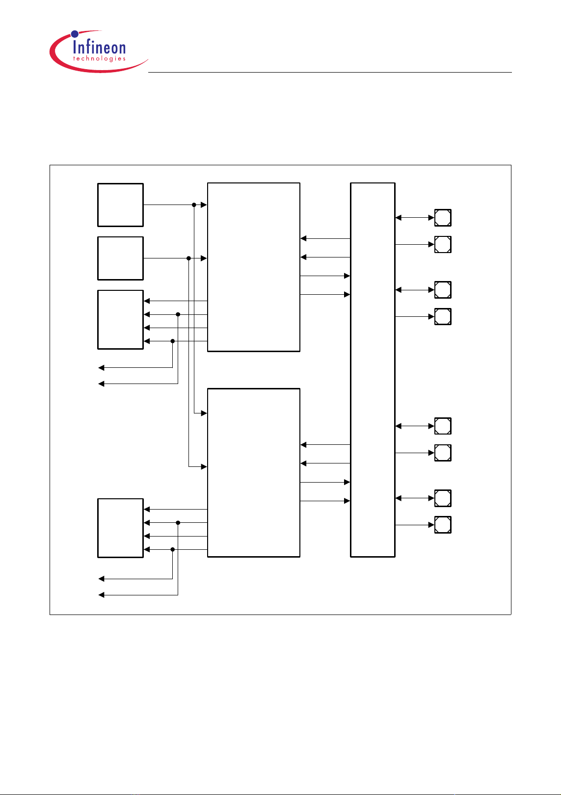
TC1161/TC1162
Functional DescriptionAdvance Information
3.7 Asynchronous/Synchronous Serial Interfaces (ASC0, ASC1)
Figure 3-3 shows a global view of the functional blocks and interfaces of the two
Asynchronous/Synchronous Serial Interfaces, ASC0 and ASC1.
f
Clock
Control
Address
Decoder
Interrupt
Control
ASC
EIR
TBIR
TIR
RIR
ASC0
Module
(Kernel)
RXD_I0
RXD_I1
RXD_O
TXD_O
A2
A2
A2
A2
P3.0 /
RXD0A
P3.1 /
TXD0A
P3.12 /
RXD0B
P3.13 /
TXD0B
To
DMA
To
DMA
ASC0_RDR
ASC0_TDR
Interrupt
Control
ASC1_RDR
ASC1_TDR
EIR
TBIR
TIR
RIR
ASC1
Module
(Kernel)
RXD_I0
RXD_I1
RXD_O
TXD_O
Figure 3-3 Block Diagram of the ASC Interfaces
Port 3
Control
A2
A2
A2
A2
P3.9 /
RXD1A
P3.8 /
TXD1A
P3.14 /
RXD1B
P3.15 /
TXD1B
MCB06211
The ASC provides serial communication between the TC1161/TC1162 and other
microcontrollers, microprocessors, or external peripherals.
The ASC supports full-duplex asynchronous communication and half-duplex
synchronous communication. In Synchronous Mode, data is transmitted or received
synchronous to a shift clock that is generated by the ASC internally. In Asynchronous
Mode, 8-bit or 9-bit data transfer, parity generation, and the number of stop bits can be
Data Sheet 51 V0.1, 2005-11

TC1161/TC1162
Functional DescriptionAdvance Information
selected. Parity, framing, and overrun error detection are provided to increase the
reliability of data transfers. Transmission and reception of data is double-buffered. For
multiprocessor communication, a mechanism is included to distinguish address bytes
from data bytes. Testing is supported by a loop-back option. A 13-bit baud rate generator
provides the ASC with a separate serial clock signal, which can be accurately adjusted
by a prescaler implemented as fractional divider.
Features
• Full-duplex asynchronous operating modes
– 8-bit or 9-bit data frames, LSB first
– Parity-bit generation/checking
– One or two stop bits
– Baud rate from 4.1Mbit/s to 0.98 bit/s (@ 66 MHz module clock)
– Multiprocessor mode for automatic address/data byte detection
– Loop-back capability
• Half-duplex 8-bit synchronous operating mode
– Baud rate from 8.25 Mbit/s to 671.4 bit/s (@ 66 MHz module clock)
• Double-buffered transmitter/receiver
• Interrupt generation
– On a transmit buffer empty condition
– On a transmit last bit of a frame condition
– On a receive buffer full condition
– On an error condition (frame, parity, overrun error)
Data Sheet 52 V0.1, 2005-11
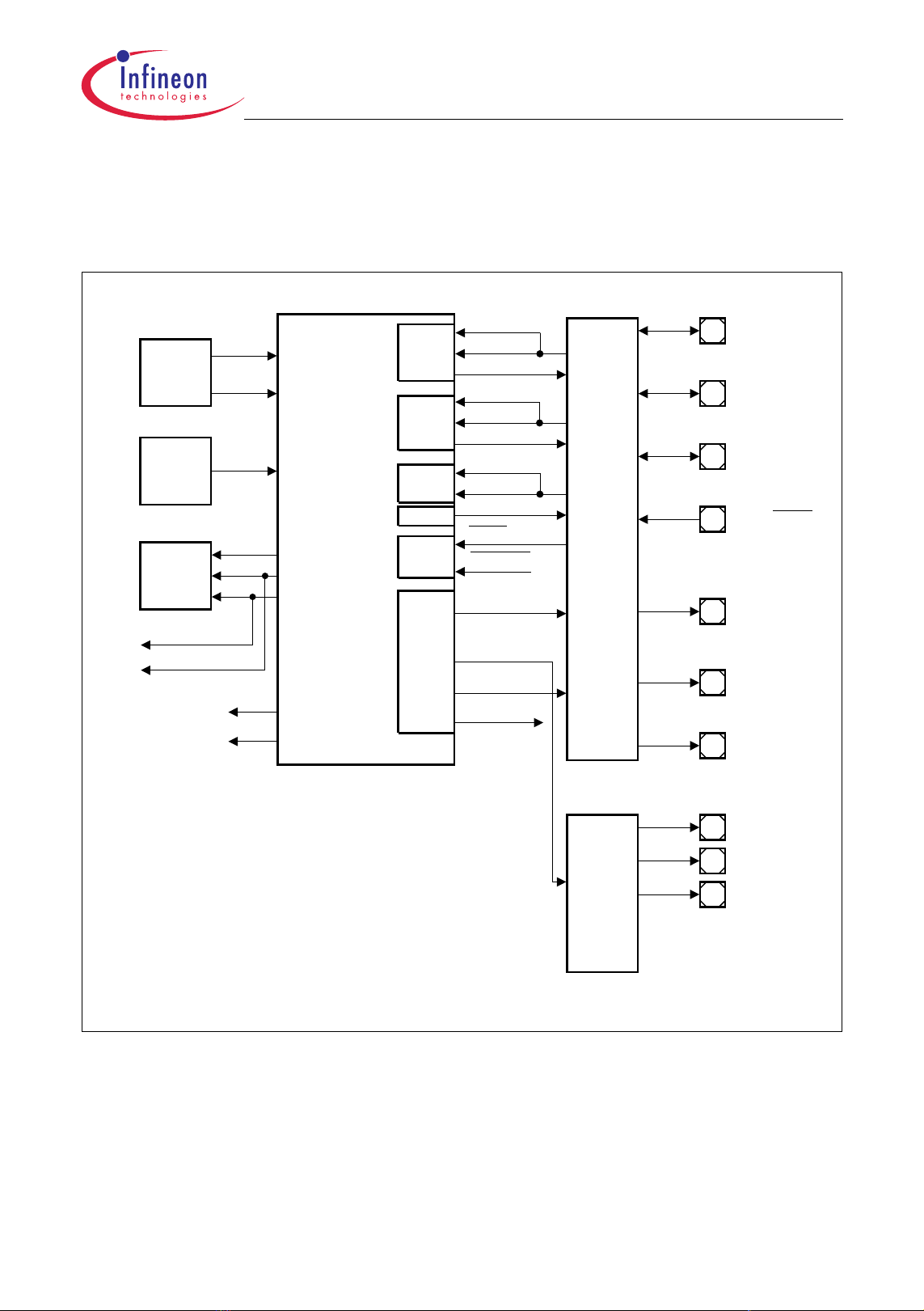
TC1161/TC1162
Functional DescriptionAdvance Information
3.8 High-Speed Synchronous Serial Interfaces (SSC0)
Figure 3-4 shows a global view of the functional blocks and interfaces of the high-speed
Synchronous Serial Interfaces, SSC0.
To
DMA
Clock
Control
Address
Decoder
Interr u p t
Control
SSC0_RDR
SSC0_TDR
M/S Select
Enable
f
SSC0
f
CLC0
EIR
TIR
RIR
MRSTA
Master
Slave
Slave
SSC0
Module
(Kernel)
1)
1)
Master
Slave
Master
MRSTB
MTSR
MTSRA
MTSRB
MRST
SCLKA
SCLKB
SCLK
SLSI1
SLSI[7:2]
SLSO[2:0]
SLSO[5:3]
SLSO6
SLSO7
1)
Port 3
Control
1)
.
.
.
P3 .4 /MTS R0
A2
P3 .3 /MRST0
A2
P3 .2 /S C L K 0
A2
P3 .7 /S L S I0
A2
P3 .5 /S L S O0
A2
P3 .7 /S L S O2
A2
P3 .8 /S L S O6
A2
P2 .1 /S L S O3
A2
P2 .8 /S L S O4
A2
Port 2
Control
1) T hese lines are not connect ed
A2
P2 .9 /S L S O5
MCB 06225
Figure 3-4 Block Diagram of the SSC Interfaces
The SSC supports full-duplex and half-duplex serial synchronous communication up to
33 MBaud (@ 66 MHz module clock). The serial clock signal can be generated by the
SSC itself (Master Mode) or can be received from an external master (Slave Mode). Data
width, shift direction, clock polarity and phase are programmable. This allows
communication with SPI-compatible devices. Transmission and reception of data is
Data Sheet 53 V0.1, 2005-11

TC1161/TC1162
Functional DescriptionAdvance Information
double-buffered. A shift clock generator provides the SSC with a separate serial clock
signal. Seven slave select inputs are available for Slave Mode operation. Eight
programmable slave select outputs (chip selects) are supported in Master Mode.
Features
• Master and Slave Mode operation
– Full-duplex or half-duplex operation
– Automatic pad control possible
• Flexible data format
– Programmable number of data bits: 2 to 16 bits
– Programmable shift direction: LSB or MSB shift first
– Programmable clock polarity: Idle low or idle high state for the shift clock
– Programmable clock/data phase: Data shift with leading or trailing edge of the shift
clock
• Baud rate generation from 503.5 bit/s to 33 Mbit/s (@ 66 MHz module clock)
• Interrupt generation
– On a transmitter empty condition
– On a receiver full condition
– On an error condition (receive, phase, baud rate, transmit error)
• Flexible SSC pin configuration
• Seven slave select inputs SLSI[7:1]
• Eight programmable slave select outputs SLSO[7:0] in Master Mode
– Automatic SLSO generation with programmable timing
– Programmable active level and enable control
in Slave Mode
Data Sheet 54 V0.1, 2005-11
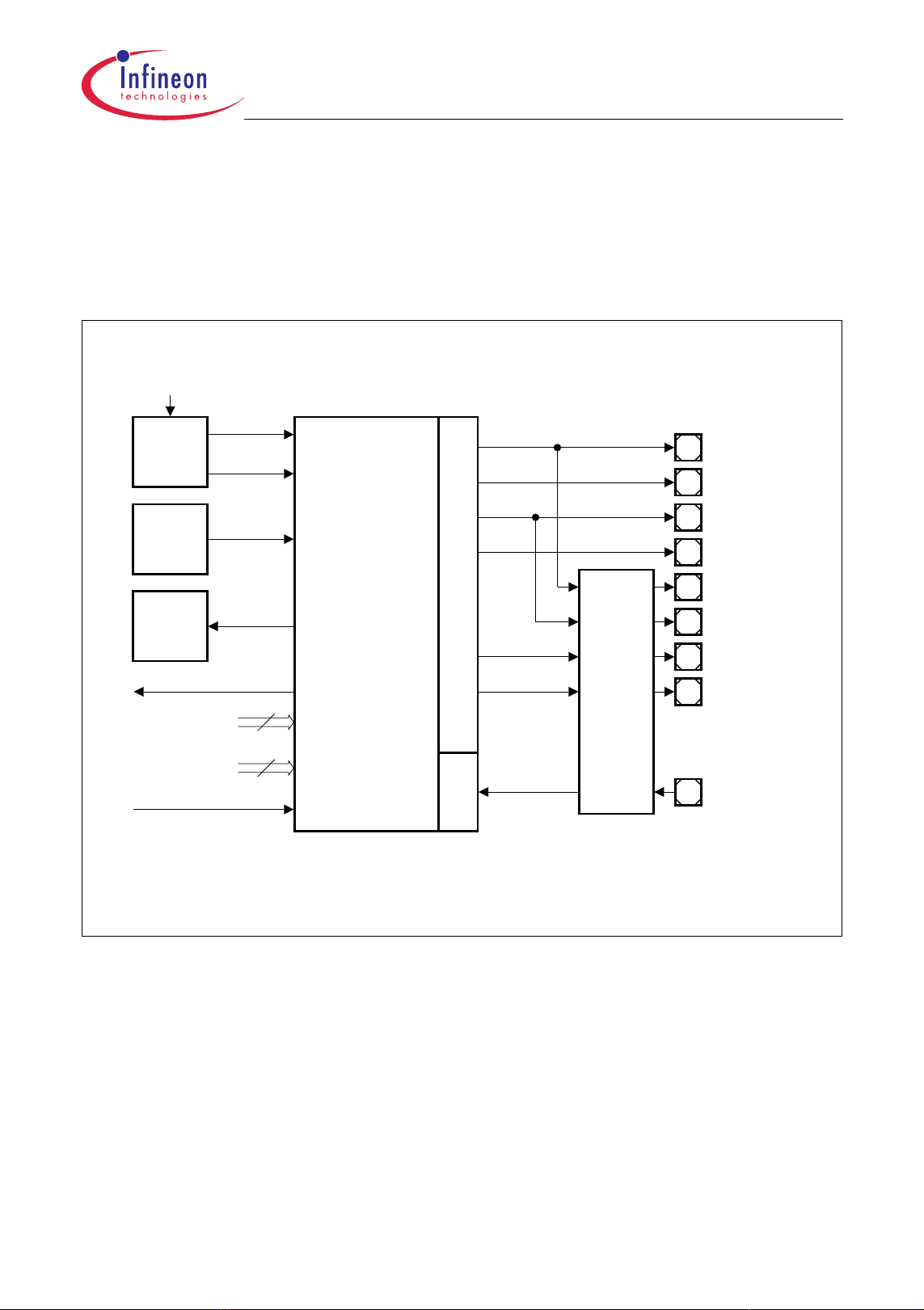
TC1161/TC1162
Functional DescriptionAdvance Information
3.9 Micro Second Bus Interfaces (MSC0)
The MSC interface provides a serial communication link typically used to connect power
switches or other peripheral devices. The serial communication link includes a fast
synchronous downstream channel and a slow asynchronous upstream channel.
Figure 3-5 shows a global view of the MSC interface signals.
SR15 (from CAN)
f
Clock
Control
Address
Decoder
Interrupt
Control
To DMA
ALTINL[15:0]
(from GPTA)
ALTINH[15:0]
EMGSTOPMSC
(from SCU)
f
2)
MSC0
CLC0
SR[1:0]
SR[3:2]
16
16
MSC0
Module
(Kernel)
Upstream
Downstream Channel
Channel
FCLP
FCLN
SOP
SON
EN0
EN1
SDI[0]
FCLP 0A
FCLN0
SOP0A
SON0
P2 .1 1 / FCLP0 B
P2 .1 2 / S OP0 B
P2 .8 / E N0 0
Port 2
Control
1)
P2 .9 / E N0 1
P2 .1 3 / S DI0
1) SDI[7:1] are connected to high level
2) Not applic able t o T C1161
MCA06255
Figure 3-5 Block Diagram of the MSC Interfaces
The downstream and upstream channels of the MSC module communicate with the
external world via nine I/O lines. Eight output lines are required for the serial
communication of the downstream channel (clock, data, and enable signals). One out of
eight input lines SDI[7:0] is used as serial data input signal for the upstream channel. The
source of the serial data to be transmitted by the downstream channel can be MSC
register contents or data that is provided at the ALTINL/ALTINH input lines. These input
lines are typically connected to other on-chip peripheral units (for example with a timer
unit like the GPTA). An emergency stop input signal makes it possible to set bits of the
serial data stream to dedicated values in emergency cases.
Data Sheet 55 V0.1, 2005-11

TC1161/TC1162
Functional DescriptionAdvance Information
Clock control, address decoding, and interrupt service request control are managed
outside the MSC module kernel. Service request outputs are able to trigger an interrupt
or a DMA request.
Features
• Fast synchronous serial interface to connect power switches in particular, or other
peripheral devices via serial buses
• High-speed synchronous serial transmission on downstream channel
f
– Serial output clock frequency:
FCL
= f
– Fractional clock divider for precise frequency control of serial clock
– Command, data, and passive frame types
– Start of serial frame: Software-controlled, timer-controlled, or free-running
– Programmable upstream data frame length (16 or 12 bits)
– Transmission with or without SEL bit
– Flexible chip select generation indicates status during serial frame transmission
– Emergency stop without CPU intervention
• Low-speed asynchronous serial reception on upstream channel
f
– Baud rate:
divided by 4, 8, 16, 32, 64, 128, or 256
MSC
– Standard asynchronous serial frames
– Parity error checker
– 8-to-1 input multiplexer for SDI lines
– Built-in spike filter on SDI lines
MSC
/2
f
MSC
Data Sheet 56 V0.1, 2005-11

TC1161/TC1162
Functional DescriptionAdvance Information
3.10 MultiCAN Controller (CAN)
Note: Section 3.10 is not applicable to TC1161.
Figure 3-6 shows a global view of the MultiCAN module with its functional blocks and
interfaces.
f
Clock
Control
CAN
f
CLC
MultiCAN Module Kernel
Address
Decoder
DMA
Interrupt
Control
INT_O
[1:0]
INT_O
[5:2]
INT_O15
Message
Object
Buffer
64
Objects
CAN Control
Linked
List
Control
CAN
Node 1
CAN
Node 0
TXDC1
RXDC1
TXDC0
RXDC0
Port 3
Control
P3.15 /
A2
TXDCAN1
P3.14 /
A2
RXDCAN1
P3.13 /
A2
TXDCAN0
P3.12 /
A2
RXDCAN0
MCA06281
Figure 3-6 Block Diagram of MultiCAN Module
The MultiCAN module contains two independently-operating CAN nodes with Full-CAN
functionality that are able to exchange Data and Remote Frames via a gateway function.
Transmission and reception of CAN frames is handled in accordance with CAN
specification V2.0 B (active). Each CAN node can receive and transmit standard frames
with 11-bit identifiers as well as extended frames with 29-bit identifiers.
Both CAN nodes share a common set of message objects. Each message object can be
individually allocated to one of the CAN nodes. Besides serving as a storage container
for incoming and outgoing frames, message objects can be combined to build gateways
between the CAN nodes or to setup a FIFO buffer.
The message objects are organized in double-chained linked lists, where each CAN
node has its own list of message objects. A CAN node stores frames only into message
objects that are allocated to the message object list of the CAN node, and it transmits
only messages belonging to this message object list. A powerful, command-driven list
controller performs all message object list operations.
Data Sheet 57 V0.1, 2005-11

TC1161/TC1162
Functional DescriptionAdvance Information
The bit timings for the CAN nodes are derived from the module timer clock (f
CAN
), and
Data Sheet 58 V0.1, 2005-11

TC1161/TC1162
Functional DescriptionAdvance Information
3.11 Micro Link Serial Bus Interface (MLI0)
The Micro Link Interface is a fast synchronous serial interface that allows data exchange
between microcontrollers of the 32-bit AUDO microcontroller family without intervention
of a CPU or other bus masters. Figure 3-7 shows how two microcontrollers are typically
connected together via their MLI interface. The MLI operates in both microcontrollers as
a bus master on the system bus.
Figure 3-7 Typical Micro Link Interface Connection
Features
• Synchronous serial communication between MLI transmitters and MLI receivers
located on the same or on different microcontroller devices
• Automatic data transfer/request transactions between local/remote controller
• Fully transparent read/write access supported (= remote programming)
Data Sheet 59 V0.1, 2005-11
TC1161/TC1162
Functional DescriptionAdvance Information
P2 .0 / TCL K 0 A
A2
Clock
Control
Address
Decoder
Interrupt
Control
To DMA
Break
f
MLI0
SR[3:0]
SR[4:7]
MLI0
Module
(Kernel)
TCLK
TREADYA
TREADYB
TREADYD
TVA LIDA
TVA LIDB
TransmitterReceiver
TVA LIDD
TDATA
RCLKA
RCLKB
RCLKD
RREADYA
RREADYB
RREADYD
RVALIDA
RVALIDB
RVALIDD
RDATAA
RDATAB
RDATAD
Port 2
Control
Port 5
Control
P2.1 / TREADY0A
A2
P2 .2 / TVA L ID0A
A2
P2.3 / TDATA0
A2
P2 .4 / RCL K 0A
A1
P2.5 / RREADY0A
A2
A1
P2.6 / RVALID0A
P2 .7 / RDA TA 0 A
A1
P5.15 / TCLK0B
A2
P5.14 / TREADY0B
A2
P5.13 / TVALID0B
A2
P5.12 / TDATA0B
A2
P5.11 / RCLK0B
A2
P5.10 / RREADY0B
A2
A2
P5.9 / RVALID0B
A2
P5 .8 / RDA TA 0 B
TC1161/T C1162 MLI B lock Diagram
Figure 3-8 Block Diagram of the MLI Module
Data Sheet 60 V0.1, 2005-11

TC1161/TC1162
Functional DescriptionAdvance Information
3.12 General Purpose Timer Array
The GPTA provides a set of timer, compare, and capture functionalities that can be
flexibly combined to form signal measurement and signal generation units. They are
optimized for tasks typical of electrical motor control applications, but can also be used
to generate simple and complex signal waveforms needed in other industrial
applications.
The TC1161/TC1162 contains one General Purpose Timer Array (GPTA0). Figure 3-9
shows a global view of the GPTA module.
GPTA
Clock Generation Unit
FPC0
FPC1
FPC2
FPC3
FPC4
FPC5
PDL0
PDL1
DCM0
DCM1
DCM2
DCM3
DIGITAL
PLL
Clock Distribution Unit
f
GPTA
Signal
GT0
GT1
GTC00
GTC01
GTC02
GTC03
Global
Timer
Cell Array
GTC30
GTC31
I/O Line Sharing Unit
Interrupt Sharing Unit
Generation Unit
Clock Bus
LTC00
LTC01
LTC02
LTC03
Local
Timer
Cell Array
LTC62
LTC63
Clock
Conn.
MCB06063
Figure 3-9 Block Diagram of the GPTA Module
Data Sheet 61 V0.1, 2005-11

TC1161/TC1162
Functional DescriptionAdvance Information
3.12.1 Functionality of GPTA0
The General Purpose Timer Array GPTA0 provides a set of hardware modules required
for high-speed digital signal processing:
• Filter and Prescaler Cells (FPC) support input noise filtering and prescaler operation.
• Phase Discrimination Logic units (PDL) decode the direction information output by a
rotation tracking system.
• Duty Cycle Measurement Cells (DCM) provide pulse-width measurement
capabilities.
• A Digital Phase Locked Loop unit (PLL) generates a programmable number of GPTA
module clock ticks during an input signal’s period.
• Global Timer units (GT) driven by various clock sources are implemented to operate
as a time base for the associated Global Timer Cells.
• Global Timer Cells (GTC) can be programmed to capture the contents of a Global
Timer on an external or internal event. A GTC may also be used to control an external
port pin depending on the result of an internal compare operation. GTCs can be
logically concatenated to provide a common external port pin with a complex signal
waveform.
• Local Timer Cells (LTC) operating in Timer, Capture, or Compare Mode may also be
logically tied together to drive a common external port pin with a complex signal
waveform. LTCs — enabled in Timer Mode or Capture Mode — can be clocked or
triggered by various external or internal events.
Input lines can be shared by an LTC and a GTC to trigger their programmed operation
simultaneously.
The following list summarizes the specific features of the GPTA unit.
Clock Generation Unit
• Filter and Prescaler Cell (FPC)
– Six independent units
– Three basic operating modes:
Prescaler, Delayed Debounce Filter, Immediate Debounce Filter
– Selectable input sources:
Port lines, GPTA module clock, FPC output of preceding FPC cell
– Selectable input clocks:
GPTA module clock, prescaled GPTA module clock, DCM clock, compensated or
uncompensated PLL clock
f
–
/2 maximum input signal frequency in Filter Modes
GPTA
• Phase Discriminator Logic (PDL)
– Two independent units
– Two operating modes (2- and 3-sensor signals)
f
–
/4 maximum input signal frequency in 2-sensor Mode, f
GPTA
/6 maximum input
GPTA
signal frequency in 3-sensor Mode
Data Sheet 62 V0.1, 2005-11

• Duty Cycle Measurement (DCM)
– Four independent units
– 0 - 100% margin and time-out handling
f
–
–
maximum resolution
GPTA
f
/2 maximum input signal frequency
GPTA
• Digital Phase Locked Loop (PLL)
– One unit
– Arbitrary multiplication factor between 1 and 65535
f
–
–
maximum resolution
GPTA
f
/2 maximum input signal frequency
GPTA
• Clock Distribution Unit (CDU)
– One unit
– Provides nine clock output signals:
f
GPTA
, divided f
clocks, FPC1/FPC4 outputs, DCM clock, LTC prescaler clock
GPTA
TC1161/TC1162
Functional DescriptionAdvance Information
Signal Generation Unit
• Global Timers (GT)
– Two independent units
– Two operating modes (Free-Running Timer and Reload Timer)
– 24-bit data width
f
–
–
maximum resolution
GPTA
f
/2 maximum input signal frequency
GPTA
• Global Timer Cell (GTC)
– 32 units related to the Global Timers
– Two operating modes (Capture, Compare and Capture after Compare)
– 24-bit data width
f
–
–
maximum resolution
GPTA
f
/2 maximum input signal frequency
GPTA
• Local Timer Cell (LTC)
– 64 independent units
– Three basic operating modes (Timer, Capture and Compare) for 63 units
– Special compare modes for one unit
– 16-bit data width
f
–
–
maximum resolution
GPTA
f
/2 maximum input signal frequency
GPTA
Interrupt Control Unit
• 111 interrupt sources, generating up to 38 service requests
Data Sheet 63 V0.1, 2005-11

TC1161/TC1162
Functional DescriptionAdvance Information
I/O Sharing Unit
• Interconnecting inputs and outputs from internal clocks, FPC, GTC, LTC, ports, and
MSC interface
Data Sheet 64 V0.1, 2005-11

TC1161/TC1162
Functional DescriptionAdvance Information
3.13 Analog-to-Digital Converter (ADC0)
Section 3.13 shows the global view of the ADC module with its functional blocks and
interfaces and the features which are provided by the module.
Clock
Control
Address
Decoder
Interrupt
Control
To DMA
f
ADC
f
CLC
SR[3:0]
SR[7:4]
V
AGND0
V
DD
V
SS
ADC0
Module
Kernel
V
DDM
SSM
V
AREF0
GPRS
EMUX0
EMUX1
ASGT
SW0TR, SW0GT
ETR, EGT
QTR, QGT
TTR, TGT
Group 0
Group 1
Analog Multiplexer
P1.14 /
A1
AD0EMUX2 (GRPS)
Port 1
Control
External
Request
Unit
(SCU)
AIN0
AIN15
AIN16
AIN30
AIN31
0
1
Die
Temperature
Measurement
P1.13 /AD0EMUX1
A1
P1.12 /AD0EMUX0
A1
8
From Ports
2
From MSC0
6
From GPTA
D
AN0
AN15
D
AN16
D
AN30
D
AN31
D
SCU_CON.DTSON
MCA06427
V
Figure 3-10 Block Diagram of the ADC Module
The ADC module has 16 analog input channels. An analog multiplexer selects the input
line for the analog input channels from among 32 analog inputs. Additionally, an external
analog multiplexer can be used for analog input extension. External Clock control,
address decoding, and service request (interrupt) control are managed outside the ADC
module kernel. External trigger conditions are controlled by an External Request Unit.
This unit generates the control signals for auto-scan control (ASGT), software trigger
control (SW0TR, SW0GT), the event trigger control (ETR, EGT), queue control (QTR,
QGT), and timer trigger control (TTR, TGT).
An automatic self-calibration adjusts the ADC module to changing temperatures or
process variations. Figure 3-10 shows the global view of the ADC module with its
functional blocks and interfaces.
Data Sheet 65 V0.1, 2005-11

Functional DescriptionAdvance Information
Features
• 8-bit, 10-bit, 12-bit A/D conversion
• Conversion time below 2.5µs @ 10-bit resolution
• Extended channel status information on request source
• Successive approximation conversion method
• Total Unadjusted Error (TUE) of ±2 LSB @ 10-bit resolution
• Integrated sample & hold functionality
• Direct control of up to 16(32) analog input channels per ADC
• Dedicated control and status registers for each analog channel
• Powerful conversion request sources
• Selectable reference voltages for each channel
• Programmable sample and conversion timing schemes
• Limit checking
• Flexible ADC module service request control unit
• Automatic control of external analog multiplexers
• Equidistant samples initiated by timer
• External trigger and gating inputs for conversion requests
• Power reduction and clock control feature
• On-chip die temperature sensor output voltage measurement
TC1161/TC1162
Data Sheet 66 V0.1, 2005-11

TC1161/TC1162
Functional DescriptionAdvance Information
3.14 Fast Analog-to-Digital Converter Unit (FADC)
The on-chip FADC module of the TC1161/TC1162 basically is a 2-channel A/D converter
with 10-bit resolution that operates by the method of the successive approximation.
As shown in Figure 3-11, the main FADC functional blocks are:
• The Input Stage — contains the differential inputs and the programmable amplifier
• The A/D Converter — is responsible for the analog-to-digital conversion
• The Data Reduction Unit — contains programmable antialiasing and data reduction
filters
• The Channel Trigger Control block — determines the trigger and gating conditions
for the two FADC channels
• The Channel Timers — can independently trigger the conversion of each FADC
channel
• The A/D Control block is responsible for the overall FADC functionality
The FADC module is supplied by the following power supply and reference voltage lines:
V
•
DDMF/VDDMF
V
•
DDAF/VDDAF
V
•
FAREF/VFAGND
:FADC Analog Part Power Supply (3.3 V)
:FADC Analog Part Logic Power Supply (1.5 V)
:FADC Reference Voltage (3.3 V)/FADC Reference Ground
Data Sheet 67 V0.1, 2005-11

TC1161/TC1162
Functional DescriptionAdvance Information
Clock
Control
Address
Decoder
Interrupt
Control
DMA
GPTA0
f
FADC
f
CLC
SR[1:0]
SR[3:2]
OUT1
OUT9
OUT18
OUT26
OUT2
OUT10
OUT19
OUT27
V
FAREF
V
FAGND
V
DDAF
V
FADC
Module
Kernel
GS[7:0]
TS[7:0]
SSAF
V
DDMF
V
SSMF
FAIN0P
FAIN0N
FAIN1P
FAIN1N
AN32
D
AN33
D
AN34
D
AN35
D
P3.10 / REQ0
A1
P3.11 / REQ1
A1
P0.14 / REQ4
A1
P0.15 / REQ5
A1
External Request Unit
(SCU)
PDOUT2
PDOUT3
MCA06445
Figure 3-11 Block Diagram of the FADC Module
Features
• Extreme fast conversion, 21 cycles of
clock (318.2 ns @ f
FADC
=66 MHz)
FADC
f
• 10-bit A/D conversion
– Higher resolution by averaging of consecutive conversions is supported
• Successive approximation conversion method
• Two differential input channels
• Offset and gain calibration support for each channel
• Differential input amplifier with programmable gain of 1, 2, 4 and 8 for each channel
• Free-running (Channel Timers) or triggered conversion modes
• Trigger and gating control for external signals
• Built-in Channel Timers for internal triggering
• Channel timer request periods independently selectable for each channel
• Selectable, programmable anti-aliasing and data reduction filter block
Data Sheet 68 V0.1, 2005-11

TC1161/TC1162
Functional DescriptionAdvance Information
3.15 System Timer
The TC1161/TC1162’s STM is designed for global system timing applications requiring
both high precision and long period.
Features
• Free-running 56-bit counter
• All 56 bits can be read synchronously
• Different 32-bit portions of the 56-bit counter can be read synchronously
• Flexible interrupt generation based on compare match with partial STM content
f
• Driven by maximum 66 MHz (=
, default after reset = f
SYS
• Counting starts automatically after a reset operation
• STM is reset by:
– Watchdog reset
– Software reset (RST_REQ.RRSTM must be set)
– Power-on reset
• STM (and clock divider STM_CLC.RMC) is not reset at a hardware reset (HDRST
0)
• STM can be halted in debug/suspend mode (via STM_CLC register)
SYS
/2)
=
The STM is an upward counter, running either at the system clock frequency f
f
fraction of it. The STM clock frequency is
f
reset is
STM
= f
/2, selected by RMC = 010B). RMC is a bit field in register STM_CLC.
SYS
STM
= f
/RMC with RMC = 0-7 (default after
SYS
SYS
or at a
In case of a power-on reset, a watchdog reset, or a software reset, the STM is reset. After
one of these reset conditions, the STM is enabled and immediately starts counting up. It
is not possible to affect the content of the timer during normal operation of the
TC1161/TC1162. The timer registers can only be read but not written to.
The STM can be optionally disabled for power-saving purposes, or suspended for
debugging purposes via its clock control register. In suspend mode of the
TC1161/TC1162 (initiated by writing an appropriate value to STM_CLC register), the
STM clock is stopped but all registers are still readable.
Due to the 56-bit width of the STM, it is not possible to read its entire content with one
instruction. It needs to be read with two load instructions. Since the timer would continue
to count between the two load operations, there is a chance that the two values read are
not consistent (due to possible overflow from the low part of the timer to the high part
between the two read operations). To enable a synchronous and consistent reading
operation of the STM content, a capture register (STM_CAP) is implemented. It latches
the content of the high part of the STM each time when one of the registers STM_TIM0
to STM_TIM5 is read. Thus, STM_CAP holds the upper value of the timer at exactly the
same time when the lower part is read. The second read operation would then read the
content of the STM_CAP to get the complete timer value.
Data Sheet 69 V0.1, 2005-11
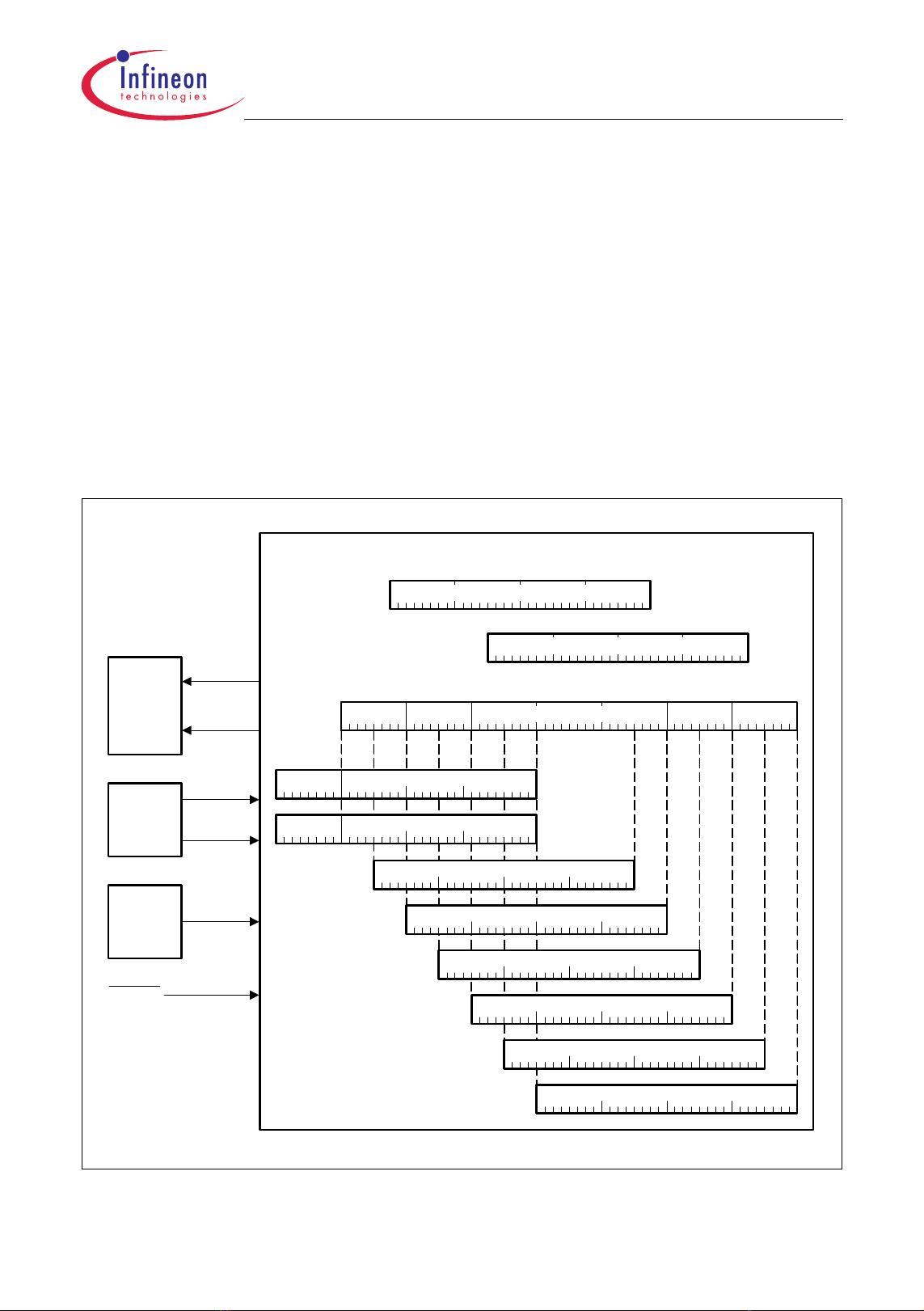
TC1161/TC1162
Functional DescriptionAdvance Information
The STM can also be read in sections from seven registers, STM_TIM0 through
STM_TIM6, that select increasingly higher-order 32-bit ranges of the STM. These can
be viewed as individual 32-bit timers, each with a different resolution and timing range.
The content of the 56-bit System Timer can be compared with the content of two
compare values stored in the STM_CMP0 and STM_CMP1 registers. Interrupts can be
generated on a compare match of the STM with the STM_CMP0 or STM_CMP1
registers.
56
The maximum clock period is 2
× f
34.60 years before overflowing. Thus, it is capable of timing the entire expected product
life-time of a system without overflowing continuously.
Figure 3-12 shows an overview on the System Timer with the options for reading parts
of the STM contents.
STM
. At f
= 66 MHz, for example, the STM counts
STM
Interrupt
Control
Clock
Control
Address
Decoder
PORST
STMIR1
STMIR0
Enable /
Disable
f
STM
STM_CMP0
55 47 39 31 23 15 7 0
00
H
00
H
STM_TIM5
STM_TIM4
31 23 15 7 0
Compare Register 0
31 23 15 7 0
STM_CMP1
56-Bit System Timer
STM_TIM3
STM_TIM2
Compare Register1
STM_CAP
STM_TIM6
STM Module
STM_TIM1
STM_TIM0
MCB06185
Figure 3-12 General Block Diagram of the STM Module Registers
Data Sheet 70 V0.1, 2005-11

TC1161/TC1162
Functional DescriptionAdvance Information
3.16 Watchdog Timer
The WDT provides a highly reliable and secure way to detect and recover from software
or hardware failure. The WDT helps to abort an accidental malfunction of the
TC1161/TC1162 in a user-specified time period. When enabled, the WDT will cause the
TC1161/TC1162 system to be reset if the WDT is not serviced within a userprogrammable time period. The CPU must service the WDT within this time interval to
prevent the WDT from causing a TC1161/TC1162 system reset. Hence, routine service
of the WDT confirms that the system is functioning as expected.
In addition to this standard “Watchdog” function, the WDT incorporates the End-ofInitialization (Endinit) feature and monitors its modifications. A system-wide line is
connected to the WDT_CON0.ENDINIT bit, serving as an additional write-protection for
critical registers (besides Supervisor Mode protection). Registers protected via this line
can only be modified when Supervisor Mode is active and bit ENDINIT = 0.
A further enhancement in the TC1161/TC1162’s WDT is its reset prewarning operation.
Instead of resetting the device upon the detection of an error immediately (the way that
standard Watchdogs do), the WDT first issues a Non-Maskable Interrupt (NMI) to the
CPU before resetting the device at a specified time period later. This step gives the CPU
a chance to save the system state to the memory for later investigation of the cause of
the malfunction; an important aid in debugging.
Features
• 16-bit Watchdog counter
• Selectable input frequency:
/256 or f
SYS
SYS
/16384
f
• 16-bit user-definable reload value for normal Watchdog operation, fixed reload value
for Time-Out and Prewarning Modes
• Incorporation of the ENDINIT bit and monitoring of its modifications
• Sophisticated Password Access mechanism with fixed and user-definable password
fields
• Proper access always requires two write accesses. The time between the two
accesses is monitored by the WDT and is limited.
• Access Error Detection: Invalid password (during first access) or invalid guard bits
(during second access) trigger the Watchdog reset generation
• Overflow Error Detection: An overflow of the counter triggers the Watchdog reset
generation.
• Watchdog function can be disabled; access protection and ENDINIT monitor function
remain enabled.
• Double Reset Detection: If a Watchdog induced reset occurs twice without a proper
access to its control register in between, a severe system malfunction is assumed
and the TC1161/TC1162 is held in reset until a power-on or hardware reset occurs.
This prevents the device from being periodically reset if, for instance, connection to
Data Sheet 71 V0.1, 2005-11

TC1161/TC1162
Functional DescriptionAdvance Information
the external memory has been lost such that system initialization could not even be
performed.
• Important debugging support is provided through the reset prewarning operation by
first issuing an NMI to the CPU before finally resetting the device after a certain
period of time.
3.17 System Control Unit
The System Control Unit (SCU) of the TC1161/TC1162 handles several system control
tasks. The system control tasks of the SCU are:
• Clock system selection and control
• Reset and boot operation control
• Power management control
• Configuration input sampling
• External Request Unit
• System clock output control
• On-chip SRAM parity control
• Pad driver temperature compensation control
• Emergency stop input control for GPTA outputs
• GPTA input IN1 control
• Pad test mode control for dedicated pins
• ODCS level 2 trace control
• NMI control
• Miscellaneous SCU control
Data Sheet 72 V0.1, 2005-11

TC1161/TC1162
Functional DescriptionAdvance Information
3.18 Boot Options
The TC1161/TC1162 booting schemes provide a number of different boot options for the
start of code execution. Table 3-6 shows the boot options available in the
TC1161/TC1162.
Table 3-6 TC1161/TC1162 Boot Selections
BRKIN
HWCFG
[3:0]
Normal Boot Options
1 0000
0001
0010
0011
1111
B
1)
B
B
B
B
TESTMODE Type of Boot BootROM
Exit Jump
Address
1 Enter bootstrap loader mode 1:
D400 0000
Serial ASC0 boot via ASC0 pins
Enter bootstrap loader mode 2:
Serial CAN boot via P3.12 and
P3.13 pins
Start from internal PFLASH A000 0000
Alternate boot mode (ABM): Start
from internal PFLASH after CRC
check is correctly executed; enter
a serial bootstrap loader mode
Defined in
ABM header
or D400 0000
2)
if
CRC check fails
Enter bootstrap loader mode 3:
D400 0000
Serial ASC0 boot via P3.12 and
P3.13 pins
H
H
H
H
others Reserved; execute stop loop –
Debug Boot Options
0 0000
B
1 Tri-state chip –
others irrel. Reserved; execute stop loop –
1) This option is not applicable to TC1161.
2) The type of the alternate bootstrap loader mode is selected by the value of the SCU_SCLIR.SWOPT[2:0] bit
field, which contains the levels of the P0.[2:0] latched in with the rising edge of the HDRST.
Data Sheet 73 V0.1, 2005-11

TC1161/TC1162
Functional DescriptionAdvance Information
3.19 Power Management System
The TC1161/TC1162 power management system allows software to configure the
various processing units so that they automatically adjust to draw the minimum
necessary power for the application. There are three power management modes:
• Run Mode
• Idle Mode
• Sleep Mode
The operation of each system component in each of these states can be configured by
software. The power-management modes provide flexible reduction of power
consumption through a combination of techniques, including stopping the CPU clock,
stopping the clocks of other system components individually, and individually clockspeed reduction of some peripheral components.
Besides these explicit software-controlled power-saving modes, special attention has
been paid to automatic power-saving in those operating units which are not required at
a certain point of time, or idle in the TC1161/TC1162. In that case, they are shut off
automatically until their operation is required again.
Table 3-7 describes the features of the power management modes.
Table 3-7 Power Management Mode Summary
Mode Description
Run The system is fully operational. All clocks and peripherals are enabled,
as determined by software.
Idle The CPU clock is disabled, waiting for a condition to return it to Run
Mode. Idle Mode can be entered by software when the processor has no
active tasks to perform. All peripherals remain powered and clocked.
Processor memory is accessible to peripherals. A reset, Watchdog
Timer event, a falling edge on the NMI
pin, or any enabled interrupt event
will return the system to Run Mode.
Sleep The system clock signal is distributed only to those peripherals
programmed to operate in Sleep Mode. The other peripheral module will
be shut down by the suspend signal. Interrupts from operating
peripherals, the Watchdog Timer, a falling edge on the NMI
pin, or a
reset event will return the system to Run Mode. Entering this state
requires an orderly shut-down controlled by the Power Management
State Machine.
In typical operation, Idle Mode and Sleep Mode may be entered and exited frequently
during the run time of an application. For example, system software will typically cause
the CPU to enter Idle Mode each time it has to wait for an interrupt before continuing its
tasks. In Sleep Mode and Idle Mode, wake-up is performed automatically when any
Data Sheet 74 V0.1, 2005-11
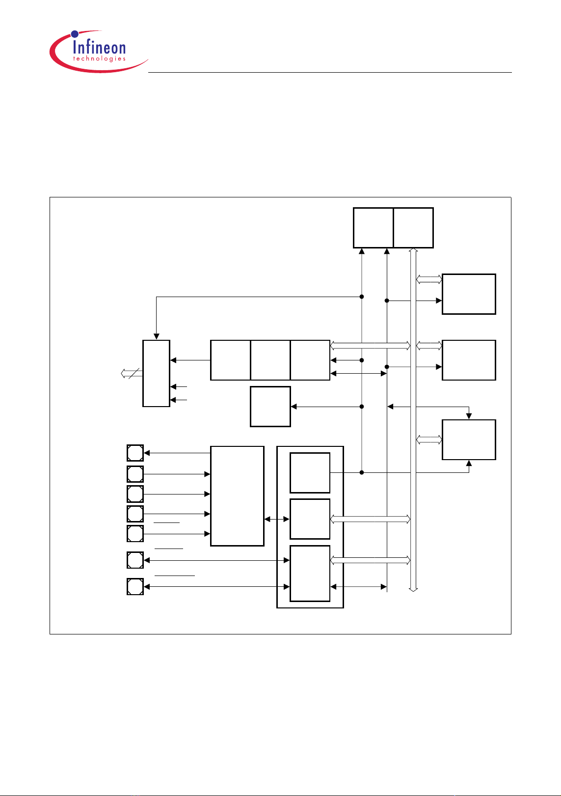
TC1161/TC1162
Functional DescriptionAdvance Information
enabled interrupt signal is detected, or when the count value (WDT_SR.WDTTIM)
changes from 7FFF
to 8000H.
H
3.20 On-Chip Debug Support
Figure 3-13 shows a block diagram of the TC1161/TC1162 OCDS system.
OCDS2[15:0]
16
Multiplexer
TDO
TDI
TMS
TCK
TRST
DMA L2
OCD S
L2
JTAG
Controller
TriCore
Watch-
dog
Timer
OCDS
OSCU
Cerberus
Debug
L1
JDI
I/F
OCDS
L1
Enable , Control and Reset
BCU
SPB
Peripheral
Unit 1
SPB
Peripheral
Unit n
DMA
Break and Suspend Signals
BRKIN
BRKOUT
MCBS
Break
Switch
System Peripheral Bus
T C1161/ TC1162 O CDS S ys t em B lock Diagram
Figure 3-13 OCDS System Block Diagram
The TC1161/TC1162 basically supports three levels of debug operation:
• OCDS Level 1 debug support
• OCDS Level 2 debug support
Data Sheet 75 V0.1, 2005-11

TC1161/TC1162
Functional DescriptionAdvance Information
OCDS Level 1 Debug Support
The OCDS Level 1 debug support is mainly assigned for real-time software debugging
purposes which have a demand for low-cost standard debugger hardware.
The OCDS Level 1 is based on a JTAG interface that is used by the external debug
hardware to communicate with the system. The on-chip Cerberus module controls the
interactions between the JTAG interface and the on-chip modules. The external debug
hardware may become master of the internal buses, and read or write the on-chip
register/memory resources. The Cerberus also makes it possible to define breakpoint
and trigger conditions as well as to control user program execution (run/stop, break,
single-step).
OCDS Level 2 Debug Support
The OCDS Level 2 debug support makes it possible to implement program tracing
capabilities for enhanced debuggers by extending the OCDS Level 1 debug functionality
with an additional 16-bit wide trace output port with trace clock. With the trace extension,
the following four trace capabilities are provided (only one of the three trace capabilities
can be selected at a time):
• Trace of the CPU program flow
• Trace of the DMA Controller transaction requests
• Trace of the DMA Controller Move Engine status information
Data Sheet 76 V0.1, 2005-11

TC1161/TC1162
Functional DescriptionAdvance Information
3.21 Clock Generation and PLL
The TC1161/TC1162 clock system performs the following functions:
• Acquires and buffers incoming clock signals to create a master clock frequency
• Distributes in-phase synchronized clock signals throughout the TC1161/TC1162’s
entire clock tree
• Divides a system master clock frequency into lower frequencies required by the
different modules for operation.
• Dynamically reduces power consumption during operation of functional units
• Statically reduces power consumption through programmable power-saving modes
• Reduces electromagnetic interference (EMI) by switching off unused modules
The clock system must be operational before the TC1161/TC1162 can function, so it
contains special logic to handle power-up and reset operations. Its services are
fundamental to the operation of the entire system, so it contains special fail-safe logic.
Features
• PLL operation for multiplying clock source by different factors
• Direct drive capability for direct clocking
• Comfortable state machine for secure switching between basic PLL, direct or
prescaler operation
• Sleep and Power-Down Mode support
The TC1161/TC1162 Clock Generation Unit (CGU) as shown in Figure 3-14 allows a
very flexible clock generation. It basically consists of an main oscillator circuit and a
Phase- Locked Loop (PLL). The PLL can converts a low-frequency external clock signal
from the oscillator circuit to a high-speed internal clock for maximum performance.
The system clock
is generated from an oscillator clock f
SYS
in either one of the four
OSC
f
hardware/software selectable ways:
• Direct Drive Mode (PLL Bypass):
In Direct Drive Mode, the TC1161/TC1162 clock system is directly driven by an
external clock signal. input, i.e.
CPU
= f
OSC
and f
SYS
= f
. This allows operation of
OSC
f
the TC1161/TC1162 with a reasonably small fundamental mode crystal.
• VCO Bypass Mode (Prescaler Mode):
f
In VCO Bypass Mode,
CPU
and f
P-Divider and K-Divider. The system clock
are derived from f
SYS
f
SYS
by the two divider stages,
OSC
is equal to f
CPU
.
• PLL Mode:
f
In PLL Mode, the PLL is running. The VCO clock
is derived from f
VCO
the P factor, multiplied by the PLL (N-Divider). The clock signals
f
derived from
by the K-Divider. The system clock f
VCO
is equal to f
SYS
f
CPU
OSC
and f
CPU
, divided by
are
SYS
.
• PLL Base Mode:
f
In PLL Base Mode, the PLL is running at its VCO base frequency and
CPU
and f
SYS
Data Sheet 77 V0.1, 2005-11

TC1161/TC1162
Functional DescriptionAdvance Information
are derived from f
equal to
XTAL1
XTAL2
BYPASS
f
CPU
Oscillator
Circuit
MOSCOGC
only by the K-Divider. In this mode, the system clock f
VCO
.
f
OSC
P
Divi-
Osc. Run
Detect.
OSCR PLL_
der
PDIV
[2:0]
Clock Generation Unit (CGU)
OSC
DISC
≥1
Lock
Detector
LOCK
Phase
Detect.
N
Divider
PLL
NDIV
[6:0]
VCO
VCO_
SEL[1:0]
f
VCO
VCO_
BYPASS
is
SYS
1:1
Divider
1
M
U
X
0
K:1
Divider
KDIV
[3:0]
SYS
FSL
PLL_
BYPASS
f
SYS
M
U
f
X
CPU
OSC_
BYPASS
Register
OSC_CON
System Control Unit (SCU)
Register PLL_CLC
MCA06083
Figure 3-14 Clock Generation Unit
Recommended Oscillator Circuits
The oscillator circuit, a Pierce oscillator, is designed to work with both, an external crystal
oscillator or an external stable clock source. It basically consists of an inverting amplifier
and a feedback element with XTAL1 as input, and XTAL2 as output.
When using a crystal, a proper external oscillator circuitry must be connected to both
pins, XTAL1 and XTAL2. The crystal frequency can be within the range of 4 MHz
C
to 25 MHz. Additionally, it is necessary to have two load capacitances
R
depending on the crystal type, a series resistor
, to limit the current. A test resistor R
X2
and CX2, and
X1
may be temporarily inserted to measure the oscillation allowance (negative resistance)
R
of the oscillator circuitry.
values are typically specified by the crystal vendor. The C
Q
X1
and CX2 values shown in Figure 3-15 can be used as starting points for the negative
resistance evaluation and for non-productive systems. The exact values and related
operating range are dependent on the crystal frequency and have to be determined and
optimized together with the crystal vendor using the negative resistance method.
Q
Data Sheet 78 V0.1, 2005-11

TC1161/TC1162
Functional DescriptionAdvance Information
Oscillation measurement with the final target system is strongly recommended to verify
the input amplitude at XTAL1 and to determine the actual oscillation allowance (margin
negative resistance) for the oscillator-crystal system.
When using an external clock signal, the signal must be connected to XTAL1. XTAL2 is
left open (unconnected). The external clock frequency can be in the range of 0 - 40 MHz
if the PLL is bypassed, and 4 - 40 MHz if the PLL is used.
The oscillator can also be used in combination with a ceramic resonator. The final
circuitry must also be verified by the resonator vendor.
Figure 3-15 shows the recommended external oscillator circuitries for both operating
modes, external crystal mode and external input clock mode. A block capacitor is
recommended to be placed between
V
DDOSC/VDDOSC3
and V
SSOSC
.
V
DDOSC
XTAL1
4 - 25
MHz
R
Q
C
X1
Fundamental
Mode Crystal
Crystal Frequency
4 MHz
8 MHz
12 MHz
16 - 25 MHz
1) Not e t hat t hese are ev aluat ion st ar t values !
C
TC1161/TC1162
R
X2
XTAL2
X2
C
33 pF
18 pF
12 pF
10 pF
V
DDOSC3
Oscillator
V
SSOSC
1)
,
C
X1
X2
V
DDOSC
f
OS C
1)
R
X2
0
0
0
0
External Clock
Signal
4 - 40
MHz
XTAL1
TC1161/TC1162
XTAL2
TC1161/TC1162 Oscillator Circuit ry
V
DDOSC3
Oscilla tor
V
SSOSC
f
OS C
Figure 3-15 Oscillator Circuitries
Note: For crystal operation, it is strongly recommended to measure the negative
resistance in the final target system (layout) to determine the optimum parameters
for the oscillator operation. Please refer to the minimum and maximum values of
the negative resistance specified by the crystal supplier.
Data Sheet 79 V0.1, 2005-11

TC1161/TC1162
Functional DescriptionAdvance Information
3.22 Power Supply
The TC1161/TC1162 has several power supply lines for different voltage classes:
• 1.5 V: Core logic, oscillator and A/D converter supply
• 3.3 V: I/O ports, Flash memories, oscillator, and A/D converter supply with reference
voltages
Figure 3-16 shows the power supply concept of the TC1161/TC1162 with the power
supply pins and its connections to the functional units.
V
DDM
(3.3V)
V
SSM
V
SSA
V
(1.5 V)
1
DDA
1
V
AREF
(3.3V)
V
AGND
2
2
ADC
V
(1.5V)
V
Ports
DDAF
SSAF
2 2
Core
V
DDMF
(3.3V)
V
SSMF
V
FAREF
(3.3V)
V
FAGND
FADC
Fl as h
Memori es
2
TC1161/TC1162
PLL
OSC
V
DDP
(3.3 V)
8
V
DDF L 3
3.3 V
1
V
DDO S C3
V
DDO S C
V
SSOSC
TC1161/TC1162 Power Supply
3
(3.3 V)
(1.5 V)
9
V
SS
7
V
DD
(1.5 V)
Figure 3-16 Power Supply Concept of TC1161/TC1162
Data Sheet 80 V0.1, 2005-11

TC1161/TC1162
Functional DescriptionAdvance Information
3.23 Identification Register Values
Table 3-8 shows the address map and reset values of the TC1161/TC1162 Identification
Registers.
Table 3-8 TC1161/TC1162 Identification Registers
Short Name Address Reset Value
SCU_ ID F000 0008
MANID F000 0070
CHIPID F000 0074
RTID F000 0078
SBCU_ID F000 0108
STM_ID F000 0208
CBS_ JDPID F000 0408
MSC0_ ID F000 0808
ASC0_ ID F000 0A08
ASC1_ ID F000 0B08
GPTA0_ ID F000 1808
DMA_ID F000 3C08
CAN_ID
1)
F000 4008
SSC0_ ID F010 0108
FADC_ ID F010 0308
ADC0_ID F010 0408
MLI0_ ID F010 C008
MCHK_ ID F010 C208
CPS_ID F7E0 FF08
CPU_ID F7E1 FE18
PMU_ID F800 0508
FLASH_ID F800 2008
DMI_ID F87F FC08
PMI_ID F87F FD08
LBCU_ID F87F FE08
LFI_ID F87F FF08
1) The address and reset value of CAN_ID is not applicable to TC1161.
H
H
H
H
H
H
H
H
H
H
H
H
H
H
H
H
H
H
H
H
H
H
H
H
H
H
002C C002
0000 1820
0000 8B02
0000 0000
0000 6A0A
0000 C006
0000 6307
0028 C001
0000 4402
0000 4402
0029 C004
001A C012
002B C012
0000 4510
0027 C012
0030 C001
0025 C006
001B C001
0015 C006
000A C005
002E C012
0041 C002
0008 C004
000B C004
000F C005
000C C005
H
H
H
H
H
H
H
H
H
H
H
H
H
H
H
H
H
H
H
H
H
H
H
H
H
H
Data Sheet 81 V0.1, 2005-11

TC1161/TC1162
Electrical ParametersAdvance Information
4 Electrical Parameters
Chapter 4 provides the characteristics of the electrical parameters which are
implementation-specific for the TC1161/TC1162.
4.1 General Parameters
The general parameters are described here to aid the users in interpreting the
parameters mainly in Section 4.2 and Section 4.3. The absolute maximum ratings and
its operating conditions are provided for the appropriate setting in the TC1161/TC1162.
4.1.1 Parameter Interpretation
The parameters listed in this section partly represent the characteristics of the
TC1161/TC1162 and partly its requirements on the system. To aid interpreting the
parameters easily when evaluating them for a design, they are marked with an two-letter
abbreviation in column “Symbol”:
• CC
Such parameters indicate Controller Characteristics which are a distinctive feature of
the TC1161/TC1162 and must be regarded for a system design.
• SR
Such parameters indicate System Requirements which must provided by the
microcontroller system in which the TC1161/TC1162 designed in.
Data Sheet 82 V0.1, 2005-11

TC1161/TC1162
Electrical ParametersAdvance Information
4.1.2 Pad Driver and Pad Classes Summary
This section gives an overview on the different pad driver classes and its basic
characteristics. More details (mainly DC parameters) are defined in Section 4.2.1.
Table 4-1 Pad Driver and Pad Classes Overview
1)
Class Power
Supply
Type Sub Class Speed
Grade
Load Leakage
Termination
A 3.3V LVTTL
I/O,
LVTTL
outputs
C 3.3V LVDS – 50
A1
(e.g. GPIO)
A2
(e.g. serial
I/Os)
A3
(e.g. BRKIN,
BRKOUT)
A4
(e.g. Trace
Clock)
6 MHz 100 pF 500 nA No
40
MHz
50 pF 6 µASeries
termination
recommended
66
MHz/
50 pF 6 µASeries
termination
recommended
(for
66
MHz
25 pF 6 µASeries
termination
recommended
– Parallel
MHz
termination
f > 25 MHz)
2)
,
100Ω±10%
D – Analog inputs, reference voltage inputs
1)Values are for T
2) In applications where the LVDS pins are not used (disabled), these pins must be either left unconnected, or
properly terminated with the differential parallel termination of 100Ω±10%.
Jmax
=125°C.
Data Sheet 83 V0.1, 2005-11

TC1161/TC1162
Electrical ParametersAdvance Information
4.1.3 Absolute Maximum Ratings
Table 4-2 shows the absolute maximum ratings of the TC1161/TC1162 parameters.
Table 4-2 Absolute Maximum Rating Parameters
Parameter Symbol Limit Values Unit Notes
Min. Max.
Ambient temperature
Storage temperature
Junction temperature
Voltage at 1.5 V power supply
pins with respect to
V
SS
1)
Voltage at 3.3 V power supply
pins with respect to
V
SS
2)
Voltage on any Class A input
pin and dedicated input pins
with respect to
V
SS
Voltage on any Class D
analog input pin with respect
to V
AGND
Voltage on any Class D
analog input pin with respect
V
to
SSAF
CPU & LMB Bus Frequency
FPI Bus Frequency
1) Applicable for VDD, V
2) Applicable for V
3) The PLL jitter characteristics add to this value according to the application settings. See the PLL jitter
parameters.
4) The ratio between f
DDP
, V
DDOSC
DDFL3, VDDM
and f
CPU
, V
DDPLL
SYS
T
A
T
ST
T
J
V
DD
V
DDP
V
IN
V
AIN,
V
AREFx
V
AINF,
V
FAREF
f
CPU
f
SYS
, and V
, and V
is fixed at 1:1.
DDAF
DDMF
SR -40 85 °C Under bias
SR -65 150 °C–
SR -40 125 °C Under bias
SR – 2.25 V –
SR – 3.75 V –
SR -0.5 V
or
DDP
+ 0.5
VWhatever is
lower
max. 3.7
SR -0.5 V
SR -0.5 V
SR – 66
SR – 66
.
.
+ 0.5
DDM
or max. 3.7
+ 0.5
DDMF
or max. 3.7
3)
3)
VWhatever is
lower
VWhatever is
lower
MHz –
MHz
4)
Note: Stresses above those listed under “Absolute Maximum Ratings” may cause
permanent damage to the device. This is a stress rating only and functional
operation of the device at these or any other conditions above those indicated in
the operational sections of this specification is not implied. Exposure to absolute
maximum rating conditions for extended periods may affect device reliability.
V
During absolute maximum rating overload conditions (
V
< VSS) the voltage on the related VDD pins with respect to ground (VSS) must
IN
> related VDD or
IN
not exceed the values defined by the absolute maximum ratings.
Data Sheet 84 V0.1, 2005-11

TC1161/TC1162
Electrical ParametersAdvance Information
4.1.4 Operating Conditions
The following operating conditions must not be exceeded in order to ensure correct
operation of the TC1161/TC1162. All parameters specified in the following table refer to
these operating conditions, unless otherwise noted.
Table 4-3 Operating Condition Parameters
Parameter Symbol Limit
Values
Unit Notes
Conditions
Min. Max.
Digital supply voltage
1)
V
DD
V
DDOSC
V
DDP
V
DDOSC3
SR 1.42 1.582)V–
SR 3.13 3.473)V For Class A
pins
(3.3V ± 5%)
Digital ground voltage
Ambient temperature under
V
DDFL3
V
SS
T
A
SR 3.13 3.473)V–
SR 0 V –
SR -40 +85 °C–
bias
Analog supply voltages – – – – See separate
specification
Page 4-91,
Page 4-98
CPU clock
Short circuit current
Absolute sum of short circuit
f
CPU
I
SC
SR –
SR -5 +5 mA
4)
Σ|ISC| SR – 20 mA See note
66
5)
MHz –
6)
7)
currents of a pin group (see
Table 4-4)
Absolute sum of short circuit
Σ|ISC| SR – 100 mA See note
7)
currents of the device
Inactive device pin current
(V
DD
=V
DDP
=0)
External load capacitance
I
C
ID
SR -1 1 mA –
L
SR – See
DC
pF Depending on
pin class
chara
cterist
ics
Data Sheet 85 V0.1, 2005-11

TC1161/TC1162
Electrical ParametersAdvance Information
1) Digital supply voltages applied to the TC1161/TC1162 must be static regulated voltages which allow a typical
voltage swing of ±5%.
2) Voltage overshoot up to 1.7 V is permissible at Power-Up and PORST
than 100 µs and the cumulated summary of the pulses does not exceed 1 h.
3) Voltage overshoot to 4 V is permissible at Power-Up and PORST
100 µs and the cumulated summary of the pulses does not exceed 1 h.
4) The TC1161/TC1162 uses a static design, so the minimum operation frequency is 0 MHz. Due to test time
restriction no lower frequency boundary is tested, however.
5) The PLL jitter characteristics add to this value according to the application settings. See the PLL jitter
parameters.
6) Applicable for digital outputs.
7) See additional document “TC1796 Pin Reliability in Overload“ for overload current definitions.
low, provided the pulse duration is less
low, provided the pulse duration is less than
Data Sheet 86 V0.1, 2005-11

TC1161/TC1162
Electrical ParametersAdvance Information
Table 4-4 Pin Groups for Overload/Short-Circuit Current Sum Parameter
Group Pins
1 TRCLK, P5.[7:0], P0.[7:6], P0.[15:14]
2 P0.[13:12], P0.[5:4], P2.[13:8], SOP0A, SON0, FCLP0A, FCLN0
3 P0.[11:8], P0.[3:0], P3.[13:11]
4 P3[10:0], P3.[15:14]
5 HDRST
TRST
, PORST, NMI, TESTMODE, BRKIN, BRKOUT, BYPASS, TCK,
, TDO, TMS, TDI, P1.[7:4]
6 P1.[3:0], P1.[11:8], P4.[3:0]
7 P2.[7:0], P1.[14:12]
8 P5.[15:8]
Data Sheet 87 V0.1, 2005-11

TC1161/TC1162
Electrical ParametersAdvance Information
4.2 DC Parameters
The electrical characteristics of the DC Parameters are detailed in this section.
4.2.1 Input/Output Pins
Table 4-5 provides the characteristics of the input/output pins of the TC1161/TC1162.
Table 4-5 Input/Output DC-Characteristics (Operating Conditions apply)
Parameter Symbol Limit Values Unit Test Conditions
Min. Max.
General Parameters
Pull-up current
1)
|I
|CC10 100 µA VIN < V
PUH
IHAmin
;
class A1/A2/Input pads.
Pull-down
current
Pin capacitance
1)
1)
(Digital I/O)
Input only Pads (
Input low voltage
class A1/A2 pins
Input high voltage
class A1/A2 pins
Ratio
V
IL/VIH
Input low voltage
class A3 pins
20 200 µA
|I
|CC10 150 µA VIN > V
PDL
20 200 µA
V
C
DDP
V
ILA
V
IHA
IO
CC – 10 pF f = 1 MHz
= 3.13 to 3.47 V = 3.3V ±5%)
SR -0.3 0.34 ×
SR 0.64 ×
V
DDP
CC 0.53 – – –
V
ILA3
SR – 0.8 V –
V
DDP
V
+
DDP
0.3 or
max. 3.6
V
IN
< V
IHAmin
;
class A3/A4 pads.
;
ILAmax
class A1/A2/Input pads.
V
IN
> V
ILAmax
;
class A3/A4 pads.
T
= 25 °C
A
V–
V Whatever is lower
Input high voltage
V
IHA3
SR 2.0 – V –
class A3 pins
Input hysteresis HYSA CC 0.1 ×
V
DDP
Input leakage
I
OZI
CC – ±3000
–V
nA ((V
current
±6000
Data Sheet 88 V0.1, 2005-11
4)
/2)-1) < VIN
DDP
< ((
otherwise
V
/2)+1)
DDP
2)

TC1161/TC1162
Electrical ParametersAdvance Information
Table 4-5 Input/Output DC-Characteristics (cont’d)(Operating Conditions
Parameter Symbol Limit Values Unit Test Conditions
Min. Max.
Class A Pads (V
Output low
voltage
3)
Output high
voltage
2)
= 3.13 to 3.47 V = 3.3V ±5%)
DDP
V
V
OLA
OHA
CC – 0.4 V IOL= 2 mA for strong driver
CC 2.4 – V IOH= -2 mA for strong
V
-
DDP
0.4
mode, (Not applicable to
Class A1 pins)
I
= 1.8 mA for medium
OL
driver mode, A2 pads
I
= 1.4 mA for medium
OL
driver mode, A1 pads
I
=370µA for weak
OL
driver mode
driver mode, (Not
applicable to Class A1
pins)
I
= -1.8 mA for medium
OH
driver mode, A1/A2 pads
I
= -370 µA for weak
OH
driver mode
–VIOH= -1.4 mA for strong
driver mode, (Not
applicable to Class A1
pins)
I
= -1 mA for medium
OH
driver mode, A1/A2 pads
I
= -280 µA for weak
OH
driver mode
Input low voltage
class A1/2 pins
Input high voltage
class A1/2 pins
V
V
ILA
IHA
SR -0.3 0.34 ×
V
DDP
SR 0.64 ×
V
DDP
V
DDP
0.3 or
V–
+
V Whatever is lower
3.6
Ratio
Input hysteresis HYSA CC 0.1 ×
Data Sheet 89 V0.1, 2005-11
V
IL/VIH
CC 0.53 – – –
–V
V
DDP
4)
TC1161/TC1162
Electrical ParametersAdvance Information
Table 4-5 Input/Output DC-Characteristics (cont’d)(Operating Conditions
Parameter Symbol Limit Values Unit Test Conditions
Min. Max.
Input leakage
current Class
A2/3/4 pins
Input leakage
I
OZA24
I
OZA1
CC – ±3000
±6000
nA ((V
<((
otherwise
/2)-1) < VIN
DDP
2)
V
CC – ±500 nA 0 V <VIN < V
DDP
DDP
/2)+1)
current
Class A1 pins
Class C Pads (V
Output low voltage
Output high
= 3.13 to 3.47 V = 3.3V ±5%)
DDP
V
V
OL
OH
CC 815 mV Parallel termination
CC 1545 mV
100 Ω±1%
voltage
Output differential
V
OD
CC 150 600 mV
voltage
Output offset
V
OS
CC 1075 1325 mV
voltage
Output impedance
R
0
CC 40 140 –
Class D Pads
see ADC Characteristics – – – –
1) Not subject to production test, verified by design / characterization.
2) Only one of these parameters is tested, the other is verified by design characterization
3) Max. resistance between pin and next power supply pin 25 Ω for strong driver mode
(verified by design characterization).
4) Function verified by design, value is not subject to production test - verified by design/characterization.
Hysteresis is implemented to avoid metastable states and switching due to internal ground bounce. It cannot
be guaranteed that it suppresses switching due to external system noise.
Data Sheet 90 V0.1, 2005-11

TC1161/TC1162
Electrical ParametersAdvance Information
4.2.2 Analog to Digital Converter (ADC0)
Table 4-6 provides the characteristics of the ADC module in the TC1161/TC1162.
Table 4-6 ADC Characteristics (Operating Conditions apply)
Parameter Symbol Limit Values Unit Test Conditions
/ Remarks
ADC digital part,
internal supply
Analog supply
voltage
V
V
DDM
DD
Min. Typ. Max.
SR 3.13 3.3 3.47
SR 1.42 1.5 1.58
1)
V–
2)
V Power supply for
Analog ground
voltage
Analog reference
voltage
16)
Analog reference
ground
16)
Analog reference
voltage range
4)16)
Analog input
voltage range
V
DDM
supply current
Power-up
calibration
time
Internal ADC
clocks
Sample time
V
SSM
V
AREFx
V
AGNDx
V
AREFx
V
AGNDx
V
AIN
I
DDM
t
PUC
f
BC
f
ANA
t
S
SR -0.1 – 0.1 V –
-
SR V
1V
SR V
0.05V
SR V
+
AGNDx
SSMx
DDM
V
-
0 V
/2 V
DDM
V
DDM
0.05
3)
AREF
1V
DDM
+
V–
1)
-
V–
+
0.05
SR V
AGNDx
–V
AREFx
V–
SR 2.5 4 mA
rms
CC – – 3840 f
ADC
CLK
CC 2 – 40 MHz fBC= f
CC 0.5 – 10 MHz f
CC 4 × (CHCONn.STC
+2)×
8 ×
t
BC
t
BC
–– µs
µs–
5)
–
× 4
ANA
= fBC/4
ANA
Data Sheet 91 V0.1, 2005-11

TC1161/TC1162
Electrical ParametersAdvance Information
Table 4-6 ADC Characteristics (cont’d) (Operating Conditions apply)
Parameter Symbol Limit Values Unit Test Conditions
Min. Typ. Max.
/ Remarks
Conversion time t
Total unadjusted
4)
error
DNL error
INL error
Gain error
10)4)
10)4)
10)4)
C
TUE
TUE
TUE
TUE
6)
DNL
INL
GAIN
CC tS+40× tBC+2× t
DIV
µs For 8-bit
conversion
t
+48× tBC+2× t
S
DIV
µs For 10-bit
conversion
t
+56× tBC+2× t
S
DIV
µs For 12-bit
conversion
CC – – ±1 LSB For 8-bit conv.
––±2 LSB For 10-bit conv.
––±4 LSB For 12-bit
7)8)
conv.
––±8 LSB For 12-bit
9)8)
conv.
CC – ±1.5 ±3.0 LSB For 12-bit conv.
8)
CC – ±1.5 ±3.0 LSB For 12-bit conv.
8)
CC – ±0.5 ±3.5 LSB For 12-bit conv.
8)
11)
11)
11)
Offset error
Input leakage
current at analog
inputs AN0, AN1
and AN31.
see Figure 4-3
Data Sheet 92 V0.1, 2005-11
10)4)
12)
TUE
I
OZ1
13)
OFF
CC – ±1.0 ±4.0 LSB For 12-bit conv.
8)
CC –1000 – 300 nA (0% V
(2%
–200 400 nA (2%
(95%
–200 1000 nA (95%
< (98%
–200 3000 nA (98%
< (100%
V
V
DDM
DDM
DDM
V
DDM
V
DDM
V
V
DDM
V
11)
) < VIN <
)
) < VIN <
)
) < VIN
)
DDM
) < VIN
)
DDM

TC1161/TC1162
Electrical ParametersAdvance Information
Table 4-6 ADC Characteristics (cont’d) (Operating Conditions apply)
Parameter Symbol Limit Values Unit Test Conditions
/ Remarks
) < VIN <
DDM
V
V
DDM
V
V
V
no
DDM
)
) < VIN <
DDM
DDM
V
DDM
DDM
V
AREF
(2%
(95%
< (98%
< (100%
V
DDM,
conversion
running
)
) < VIN
)
) < VIN
)
DDM
<
Input leakage
current at analog
inputs AN2 to
AN30, see
Figure 4-3
Input leakage
current at
V
AREF
I
I
OZ1
OZ2
13)
Min. Typ. Max.
CC –1000 – 200 nA (0% V
–200 300 nA (2%
–200 1000 nA (95%
–200 3000 nA (98%
CC – – ±1 µA0V<V
Input current at
AREF
16)
V
Total capacitance
of the voltage
reference
inputs
15)16)
Switched
capacitance at
the positive
reference voltage
16)
input
Resistance of the
reference voltage
input path
15)
Total capacitance
of the analog
inputs
15)
Switched
capacitance at
the analog
voltage inputs
I
AREF
C
AREFTOT
C
AREFSW
R
AREF
C
AINTOT
C
AINSW
CC – 35 75 µA
rms
CC – – 25 pF
CC – 15 20 pF
0V<V
14)
V
DDM
8)
8)17)
AREF
CC – 1 1.5 kΩ 500 Ohm
increased for
AN[1:0] used as
reference input
CC – – 25 pF
CC – – 7 pF
5)8)
8)18)
<
8)
Data Sheet 93 V0.1, 2005-11

TC1161/TC1162
Electrical ParametersAdvance Information
Table 4-6 ADC Characteristics (cont’d) (Operating Conditions apply)
Parameter Symbol Limit Values Unit Test Conditions
/ Remarks
8)
ON resistance of
the transmission
gates in the
analog voltage
path
R
AIN
Min. Typ. Max.
CC – 1 1.5 kΩ
ON resistance for
the ADC test
(pull-down for
AIN7)
Current through
resistance for the
ADC test (pulldown for AIN7)
1) Voltage overshoot to 4 V are permissible, provided the pulse duration is less than 100 µs and the cumulated
summary of the pulses does not exceed 1 h.
2) Voltage overshoot to 1.7 V are permissible, provided the pulse duration is less than 100 µs and the cumulated
summary of the pulses does not exceed 1 h.
3) A running conversion may become inexact in case of violating the normal operating conditions (voltage
overshoot).
4) If a reduced reference voltage in a range of
If the reference voltage is reduced with the factor k (k<1), then TUE, DNL, INL Gain and Offset errors increase
with the factor 1/k.
If a reduced reference voltage in a range of 1 V to
ADC speed and accuracy.
5) Current peaks of up to 6 mA with a duration of max. 2 ns may occur
6) TUE is tested at
7) ADC module capability.
8) Not subject to production test, verified by design / characterization.
9) Value under typical application conditions due to integration (switching noise, etc.).
10) The sum of DNL/INL/Gain/Offset errors does not exceed the related TUE total unadjusted error.
11) For 10-bit conversions the DNL/INL/Gain/Offset error values must be multiplied with factor 0.25.
For 8-bit conversions the DNL/INL/Gain/Offset error values must be multiplied with 0.0625.
12) The leakage current definition is a continuous function, as shown in Figure 4-3. The numerical values defined
determine the characteristic points of the given continuous linear approximation - they do not define step
function.
13) Only one of these parameters is tested, the other is verified by design characterization.
I
14)
AREF_MAX
with a duration of up to
needs a total charge of
All ADC conversions with a duration longer than
is valid for the minimum specified conversion time. The current flowing during an ADC conversion
V
AREF
R
AIN7T
I
AIN7T
CC 200 300 1000 Ω Test feature
CC – 15
rms
V
/2 to V
DDM
=3.3V, V
t
=25µs can be calculated with the formula I
C
Q
= 150pC from V
CONV
= 0 V and V
AGND
AREF
t
DDM
V
/2 is used, then there are additional decrease in the
DDM
=3.3V
DDM
.
= 25µs consume an I
C
available only for
AIN7
8)
30
peak
mA Test feature
available only for
AIN7
8)
is used, then the ADC converter errors increase.
AREF_MAX
AREF_MAX
= Q
= 6µA.
. Every conversion
CONV/tC
Data Sheet 94 V0.1, 2005-11

TC1161/TC1162
f
Electrical ParametersAdvance Information
15) For the definition of the parameters see also Figure 4-2.
16) Applies to AIN0 and AIN1, when used as auxiliary reference inputs.
17) This represents an equivalent switched capacitance. This capacitance is not switched to the reference voltage
at once. Instead of this smaller capacitances are successively switched to the reference voltage.
V
18) The sampling capacity of the conversion C-Network is pre-charged to
Because of the parasitic elements the voltage measured at AINx is lower then
A/D Converter Module
CLC
Fractional
Divider
Arbiter
(1:20)
f
DIV
f
TIMER
Programmable
Clock Divider
(1:1) t o (1:256)
CON.CTC CHCONn.STC
Cont rol Unit
(Timer)
f
BC
1:4
Control/ St atus Logic
External Trigger Logic
External Multip lex er Logi c
Request Generation Logic
/2 before the sampling moment.
AREF
V
/2.
AREF
Sample
f
ANA
Programmable
Counter
Interrupt Logi c
Time
t
S
MCA04657_mod
Figure 4-1 ADC0 Clock Circuit
Data Sheet 95 V0.1, 2005-11
TC1161/TC1162
Electrical ParametersAdvance Information
R
EXT
V
=
AIN
C
EXT
ANx
V
AGNDx
R
AIN7T
R
C
AINTOT
AIN, On
- C
AINSW
C
AINSW
Reference Voltage Input Circuitry
R
Analog Input Circuitry
V
AREF
V
V
AGNDx
AREFx
C
AREFTOT
AREF, On
- C
AREFSW
C
AREFSW
Analog_InpRefDiag
Figure 4-2 ADC0 Input Circuits
Data Sheet 96 V0.1, 2005-11
 Loading...