

Marketing Information
T 739 N
C
European PowerSemiconductor and
Electronics Company
+
ø3,5
deepth =
A
H
A 4,8 x
DIN 46
A 2,8 x 0,8
DIN 46 244
G
8,5 max
VWK Aug.

T 739 N
Elektrische Eigenschaften
Electrical properties
3600 3800 4000
3600 3800 4000
3700 3900 4100
Thermische Eigenschaften
Thermal properties
Kühlung
two-sided cooling
Mechanische Eigenschaften
Mechanical properties
Höchstzulässige Werte Maximum rated values
Periodische Vorwärts- und RückwärtsSpitzensperrspannung
repetitive peak forward off-state and
reverse voltages
tvj = -40°C...t
vj max
V
DRM
, V
RRM
4200
V
Vorwärts-Stoßspitzensperrspannung non-repetitive peak forward off-state
voltage
Rückwärts-Stoßspitzensperrspannung non-repetitive peak reverse voltage tvj = +25°C...t
Durchlaßstrom-Grenzeffektivwert RMS on-state current I
Dauergrenzstrom average on-state current tc = 85°C I
tvj = -40°C...t
vj max
vj max
V
DSM
V
RSM
TRMSM
TAVM
tc = 55°C 1100 A
Stoßstrom-Grenzwert surge current tvj = 25°C, tp = 10 ms I
tvj = t
, tp = 10 ms 15000 A
vj max
Grenzlastintegral
I2 t-value
tvj = 25°C, tp = 10 ms
tvj = t
, tp = 10 ms 1125000
vj max
TSM
I2 t
Kritische Stromsteilheit critical rate of rise of on-state current f = 50 Hz, iGM= 1 A, diG/dt = 1 A/µs (diT/dt)
Kritische Spannungssteilheit critical rate of rise of off-state voltage tvj = t
, vD = 67% V
vj max
DRM
(dv/dt)
Charakteristische Werte Characteristic values
Durchlaßspannung on-state voltage tvj = t
Schleusenspannung threshold voltage tvj = t
Ersatzwiderstand slope resistance tvj = t
Zündstrom gate trigger current tvj = 25 °C, vD = 6 V I
Zündspannung gate trigger voltage tvj = 25 °C, vD = 6 V V
Nicht zündender Steuerstrom gate non-trigger current tvj = t
Nicht zündende Steuerspannung gate non-trigger voltage tvj = t
Haltestrom holding current
Einraststrom latching current
Vorwärts- und Rückwärts-Sperrstrom forward off-state and reverse currents tvj = t
Zündverzug gate controlled delay time tvj=25°C, iGM = 1 A, diG/dt = 1 A/µs t
Freiwerdezeit circuit commutated turn-off time siehe Techn.Erl./see Techn. Inf. t
, iT = 3300 A v
vj max
vj max
vj max
, vD = 6 V I
vj max
tvj = t
, vD = 0,5 V
vj max
vj max
, vD = 0,5 V
DRM
DRM
tvj = 25 °C, vD = 12 V, RA = 4,7 Ω
tvj = 25 °C,vD = 6 V, RGK ≥ 10 Ω
iGM = 1 A, diG /dt = 1 A/µs, tg = 20 µs
= V
vj max, vD
DRM
, vR = V
RRM
V
r
T
GT
GD
V
I
H
I
L
iD, i
gd
q
T
T(TO)
GT
GD
R
= V
= V
cr
DRM
RRM
4200
4300
V
V
1750 A
730 A
16500 A
1361000
A2s
A2s
cr
50 A/µs
1000 V/µs
max. 3,1 V
1,15 V
0,59
mΩ
max. 300 mA
max. 2,5 V
max. 20 mA
max. 10 mA
max. 0,4 V
max. 300 mA
max. 2000 mA
max. 100 mA
max. 1,6 µs
typ. 450 µs
Innerer Wärmewiderstand für beidseitige
thermal resistance, junction to case for
Θ =180° el, sin
R
thJC
max. 0,0215 °C/W
DC max. 0,0200 °C/W
für anodenseitige Kühlung for anode-sided cooling
Θ =180° el, sin
R
thJC(A)
max. 0,0375 °C/W
DC max. 0,0360 °C/W
für kathodenseitige Kühlung for cathode-sided cooling
Θ =180° el, sin
R
thJC(K)
max. 0,0465 °C/W
DC max. 0,0450 °C/W
Übergangs-Wärmewiderstand thermal resistance, case to heatsink beidseitig/two-sided R
thCK
max. 0,004 °C/W
einseitig/one-sided max. 0,008 °C/W
Höchstzul.Sperrschichttemperatur max. junction temperature t
Betriebstemperatur operating temperature t
Lagertemperatur storage temperature t
Si-Elemente mit Druckkontakt Si-pellet with pressure contact
vj max
c op
stg
120 °C
-40...+120 °C
-40...+150 °C
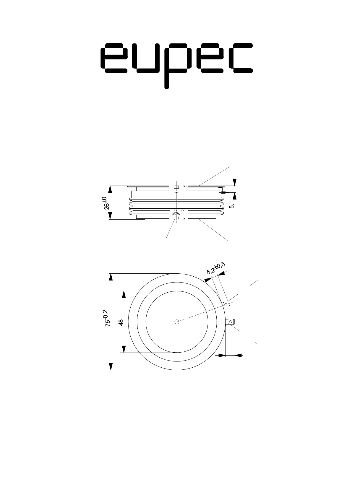
Anpreßkraft clamping force F 15...24 kN
Gewicht weight G typ. 550 g
Kriechstrecke creepage distance 25 mm
Feuchteklasse humidity classification DIN 40040 C
Schwingfestigkeit vibration resistance f = 50 Hz 50 m/s²
Maßbild, anliegend outline, attached

i
[A]
T
3500
3000
2000
1500
P
[W]
3000
TAV
2000
T 739 N
180°
Θ
0
Θ = 30°
60°
90°
120°
1000
500
0
T 739 N / 1
1,0 1,5 2,0 2,5 3,0 3,50,5
Bild / Fig. 1
Grenzdurchlaßkennlinie / Limiting on-state characteristic,
iT = f(vT), tvj = t
vj max
140
120
t
c
[°C]
100
80
60
40
20
0 800
T 739 N / 3
Θ = 60°
90° 120° 180°
Bild / Fig. 3
Höchstzulässige Gehäusetemperatur / Max. allowable case temperature
tC = f(I
Beidseitige Kühlung / Two-sided cooling
TAVM
)
Parameter: Stromflußwinkel / Current conduction angle θ
I
TAVM
vT [V]
[A]
1000
0
0 800
T 739 N / 2
200
400 600 1000
I
TAV
[A]
1200
Bild / Fig. 2
Durchlaßverlustleistung / On-state power loss P
Parameter: Stromflußwinkel / Current conduction angle θ
TAV
= f(I
TAV
)
140
Θ
0
t
c
[°C]
120
100
Θ
0
80
60
40
20
1200200 400 600 1000
0 800
T 739 N / 4
Θ = 60°
90°
120° 180°
I
TAVM
[A]
1200200 400 600 1000
Bild / Fig. 4
Höchstzulässige Gehäusetemperatur / Max . allowable case temperature
tC = f(I
Anodenseitige Kühlung / Anode-sided cooling
TAVM
)
Parameter: Stromflußwinkel / Current conduction angle θ
4000
t
c
[°C]
0 Θ 0 Θ
3000
Θ = 30°
60°
90°
120°
2000
1000
0
0
T 739 N / 5
1000
Bild / Fig. 5
Durchlaßverlustleistung / On-state power loss P
Parameter: Stromflußwinkel / Current conduction angle θ
180°
TAV
= f(I
I
TAV
TAV
DC
140
120
t
c
[°C]
100
80
60
[A]
40
20
2000500 1500
0
T 739 N / 6
Θ = 60°
90° 120° 180°
1000
I
TAVM
DC
2000500 1500
[A]
Bild / Fig. 6
)
Höchstzulässige Gehäusetemperatur / Max . allowable case temperature
tC = f(I
Beidseitige Kühlung / Two-sided cooling
TAVM
)
Parameter: Stromflußwinkel / Current conduction angle θ

T 739 N
140
120
t
c
[°C]
100
80
60
40
20
0 800
T 739 N / 7
Θ = 60° 90°
120° 180° DC
12001000
Bild / Fig. 7
Höchstzulässige Gehäusetemperatur / Max. allowable case temperature
tC = f(I
Anodenseitige Kühlung / Anode-sided cooling
TAVM
)
Parameter: Stromflußwinkel / Current conduction angle θ
2
10
6
4
t
2
gd
[µs]
1
10
6
4
2
0
10
6
4
2
-1
10
1
10
T 739 N / 9
2 4 6
10
2
2 4 6
3
10
Bild / Fig. 9
Zündverzug / Gate controlled delay time tgd = f(iG)
tvj = 25 °C, diG/dt = iGM/1µs
I
[A]
TAVM
max
typ
2 4 6
i
[mA]
GM
0 Θ
20
10
v
[V]
8
6
G
4
c
b
a
2
1,0
0,8
0,6
0,4
0,2
0,1
1
1600200 400 600 1400
10
T 739 N / 8
2 4 6
10
2
2 4 6
10
3
2 4 6
iG [mA]
4
10
Bild / Fig. 8
Steuercharakteristik mit Zündbereichen / Gate characteristic with trigging
areas vG = f(iG), VD = 6 V
Parameter: a b c
––––––––––––––––––––––––––––––––––––––––––––––––––––––––––
Steuerimpulsdauer / trigger puls duration tg [ms] 10 1 0,5
––––––––––––––––––––––––––––––––––––––––––––––––––––––––––
Höchstzulässige Spitzensteuerverlustleistung /
Max. rated peak gate power dissipation [W] 20 40 60
––––––––––––––––––––––––––––––––––––––––––––––––––––––––––
4
10
9
8
7
6
Q
r
5
[µAs]
4
3
2
3
10
4
10
0
10
T 739 N / 10
2 3 4 5 6 7 8
iTM=1000A
1
10
2 3 4 5 6 7 8
-di/dt [A/µs]
2
10
Bild / Fig. 10
Sperrverzögerungsladung / Recovered charge Qr = f(di/dt)
tvj = t
Parameter: Durchlaßstrom / On-state current i
vj max
, vR = 0,5 V
, vRM = 0,8 V
RRM
RRM
TM
0,030
0,025
Z
(th)JC
[°C/W]
Θ
0
0,020
0,015
0,010
0,005
0
-3
2 4 6 2 4 6 2 4 6 2 4 62 4 6
10
T 739 N / 11
Θ=
30°
60°
90°
120°
180°
-2
10
-1
10
0
10
Bild / Fig. 11
Transienter innerer Wärmewiderstand / Transient thermal impedance
Z
= f(t)
thJC
Beidseitige Kühlung / Two-sided cooling
Parameter: Stromflußwinkel / current conduction angle θ
10
t [s]
0,05
Θ
0
0,04
Z
(th)JC
[°C/W]
0,03
0,02
Θ=
0,01
1
10
0
2
-3
2 4 6 2 4 6 2 4 6 2 4 62 4 6
10
T 739 N / 12
30°
60°
90°
120°
180°
-2
10
-1
10
0
10
1
10
2
10
t [s]
Bild / Fig. 12
Transienter innerer Wärmewiderstand / Transient thermal impedance
Z
= f(t)
thJC
Anodenseitige Kühlung / Anode-sided cooling
Parameter: Stromflußwinkel / current conduction angle θ

T 739 N
0,030
0 Θ
0,025
Z
(th)JC
[°C/W]
0,020
0,015
0,010
0,005
0
-3
2 4 6 2 4 6 2 4 6 2 4 62 4 6
10
T 739 N / 13
Θ=
30°
60°
90°
120°
180°
DC
-2
10
-1
10
0
10
Bild / Fig. 13
Transienter innerer Wärmewiderstand / Transient thermal impedance
Z
= f(t)
thJC
Beidseitige Kühlung / Two-sided cooling
Parameter: Stromflußwinkel / current conduction angle θ
Analytische Elemente des transienten Wärmewiderstandes Z
Analytical elements of transient thermal impedance Z
per arm for DC
thJC
Beidseitig / Two-sided
R
τ
thn
[s]
n
Pos. n
[°C/W]
1 2 3 4 5
0,0001 0,0019 0,0041 0,0072 0,0067
0,0008 0,0073 0,062 0,204 1,8
1
10
t [s]
pro Zweig für DC
thJC
0,05
0 Θ
0,04
Z
(th)JC
[°C/W]
0,03
0,02
Θ=
10
30°
60°
90°
120°
180°
DC
-2
-1
10
0
10
1
10
2
10
t [s]
0,01
0
2
10
-3
2 4 6 2 4 6 2 4 6 2 4 62 4 6
10
T 739 N / 14
Bild / Fig. 14
Transienter innerer Wärmewiderstand / Transient thermal impedance
Z
= f(t)
thJC
Anodenseitige Kühlung / Anode-sided cooling
Parameter: Stromflußwinkel / current conduction angle θ
Anodenseitig / Anode-sided
R
τ
thn
[s]
n
Pos. n
[°C/W]
1 2 3 4 5
0,0001 0,0019 0,0041 0,0061 0,0238
0,0008 0,0073 0,062 0,162 6,5
Kathodenseitig / Cathode-sided
R
τ
thn
[s]
n
Pos. n
[°C/W]
1 2 3 4 5
0,0001 0,0019 0,0041 0,0065 0,0324
0,0008 0,0073 0,062 0,185 6,8
Analytische Funktion / Analytical function:
n
Z
thJC
max
= R
Σ
n=1
(1-e )
thn
t
-
τ
n
 Loading...