

Infineon IRPS5401 User Manual

Application Note Please read the Important Notice and Warnings at the end of this document V 1.2
www.infineon.com page 1 of 63 2018-12-12
5 Output PMIC Controller/ IRPS5401
User guide with DB295 and DB296 demo boards
About this document
Scope and purpose
Note: The following information is given as a description of the device only and shall not be regarded as a
description or warranty of a certain functionality, condition or quality of the device.
This application note is intended to provide a description of the operation of IRPS5401 and the performance of
the DB295 (orderable as EVAL_PS5401-25 or EVAL_PS5401-40) and DB296 (orderable as EVAL_PS5401-INT)
demo boards.
It is assumed that the user is already familiar with the datasheet and functions of the IRPS5401 device.
Intended audience
FAEs and customer engineers
UG_201708_PL17_10

Application Note 2 of 63 V 1.2
2018-12-12
5 Output PMIC Controller/ IRPS5401
User guide with DB295 and DB296 demo boards
Introduction
Table of contents
About this document ....................................................................................................................... 1
Table of contents ............................................................................................................................ 2
1 Introduction .......................................................................................................................... 3
2 I2C ADDRESS, PMBUS address, and address offset ..................................................................... 4
2.1 ADDR_PROT Pin ....................................................................................................................................... 6
2.2 TEST ADDRESS 0Ah ................................................................................................................................. 8
3 LDO Operation ....................................................................................................................... 9
3.1 Source only mode ................................................................................................................................... 9
3.2 Sink/Source (Tracking) mode ................................................................................................................. 9
3.3 Fault settings ......................................................................................................................................... 10
4 Switcher Operation ............................................................................................................... 11
4.1 Setting the Switching Frequency .......................................................................................................... 12
4.2 AOT Mode ............................................................................................................................................... 12
4.3 External Sync ......................................................................................................................................... 14
4.4 Current Sense and Over Current Settings ............................................................................................ 15
4.5 Current Reporting Accuracy .................................................................................................................. 16
4.6 Over Voltage Settings at Start-up and Shut Down ............................................................................... 16
4.7 Over Voltage Settings under Steady State ........................................................................................... 17
4.8 Under Voltage Settings ......................................................................................................................... 18
4.9 Over Temperature ................................................................................................................................. 19
4.10 ½ Scaling of VOUT ................................................................................................................................. 20
5 External Power Stage ............................................................................................................ 22
5.1 ISENSE AMP Gain Settings .................................................................................................................... 23
5.2 Layout Concerns .................................................................................................................................... 24
5.3 VSENSE FEEDBACK ................................................................................................................................ 24
5.4 VIN Decoupling ...................................................................................................................................... 25
6 C+D Operation ...................................................................................................................... 26
6.1 Current Balance ..................................................................................................................................... 26
6.2 Over Current Protection ........................................................................................................................ 26
7 MTP Programming................................................................................................................. 27
7.1 Programming a Single Config File ........................................................................................................ 27
7.1 Generating Multiple Config Files (*.mic) ............................................................................................... 27
7.1 Using the Multiple Config File Index Feature........................................................................................ 28
8 Modulator Details .................................................................................................................. 31
8.1 Emulated Current Mode Control with Digital P and I ........................................................................... 31
8.1 Description of Excel PI Calculator Tool ................................................................................................ 32
8.2 Recommended Circuit and Operating Parameters for Internal Switchers from the Data Sheet ....... 34
9 Efficiency, Power Dissipation, and Temp Rise ........................................................................... 35
9.1 GUI Efficiency Tool ................................................................................................................................ 35
9.2 Demo Board Efficiency and Temp Rise ................................................................................................. 37
10 DB295 and DB296 Details ....................................................................................................... 41
11 General Design Recommendations and Advisements ................................................................. 46
12 Typical Performance ............................................................................................................. 47
Application Note 3 of 63 V 1.2
2018-12-12
5 Output PMIC Controller/ IRPS5401
User guide with DB295 and DB296 demo boards
1 Introduction
This document will describe the operation of the IRPS5401 PMIC. This document will also cover the details of
the DB295 (available as EVAL_PS5401-25 for 25A power stage and EVAL_PS5401-40 for 40A power stage) and
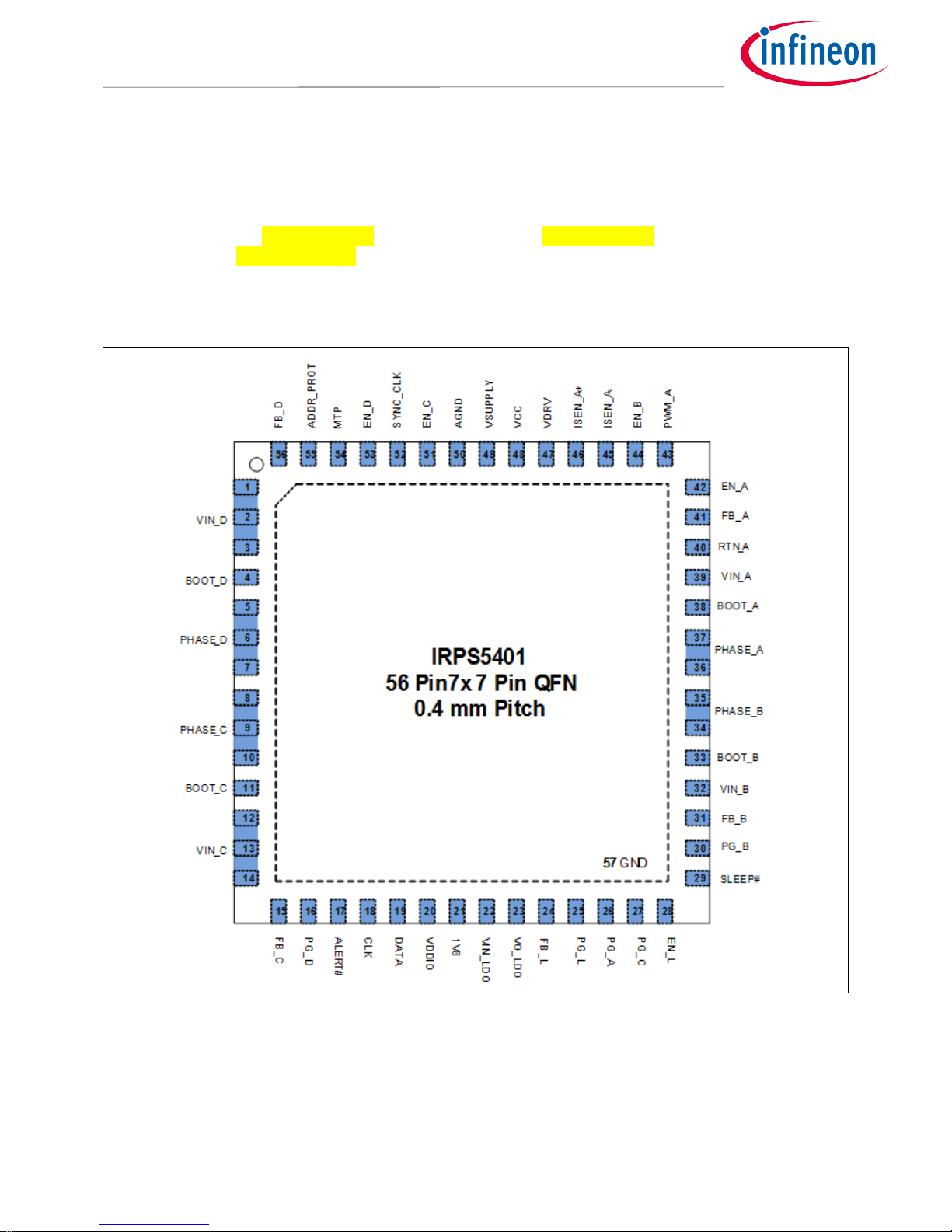
DB296 (available as EVAL_PS5401-INT) IRPS5401 demo boards. IRPS5401 is a 56 pin, 7x7 mm PMIC. It has 4
switching outputs and 1 LDO output. SW-A and SW-B have a max rated current of 2 A. SW-A can be configured
to drive an external power-stage. SW-C and SW-D have a max rating of 4 A. The LDO has a max rating of 0.5 A
and can be configured as source only mode or sink-source (tracking) mode.
Figure 1 Pinout diagram
For more information see:
IRPS5401; Data Sheet
UN0049; Description of PMBus commands in IRPS5401
UN0065; List of and functional description of I2C Registers (Customer RegMap)
TB0035; Programming Guide for IRPS5401
Application Note 4 of 63 V 1.2
2018-12-12
5 Output PMIC Controller/ IRPS5401
User guide with DB295 and DB296 demo boards
2 I2C ADDRESS, PMBUS address, and address offset
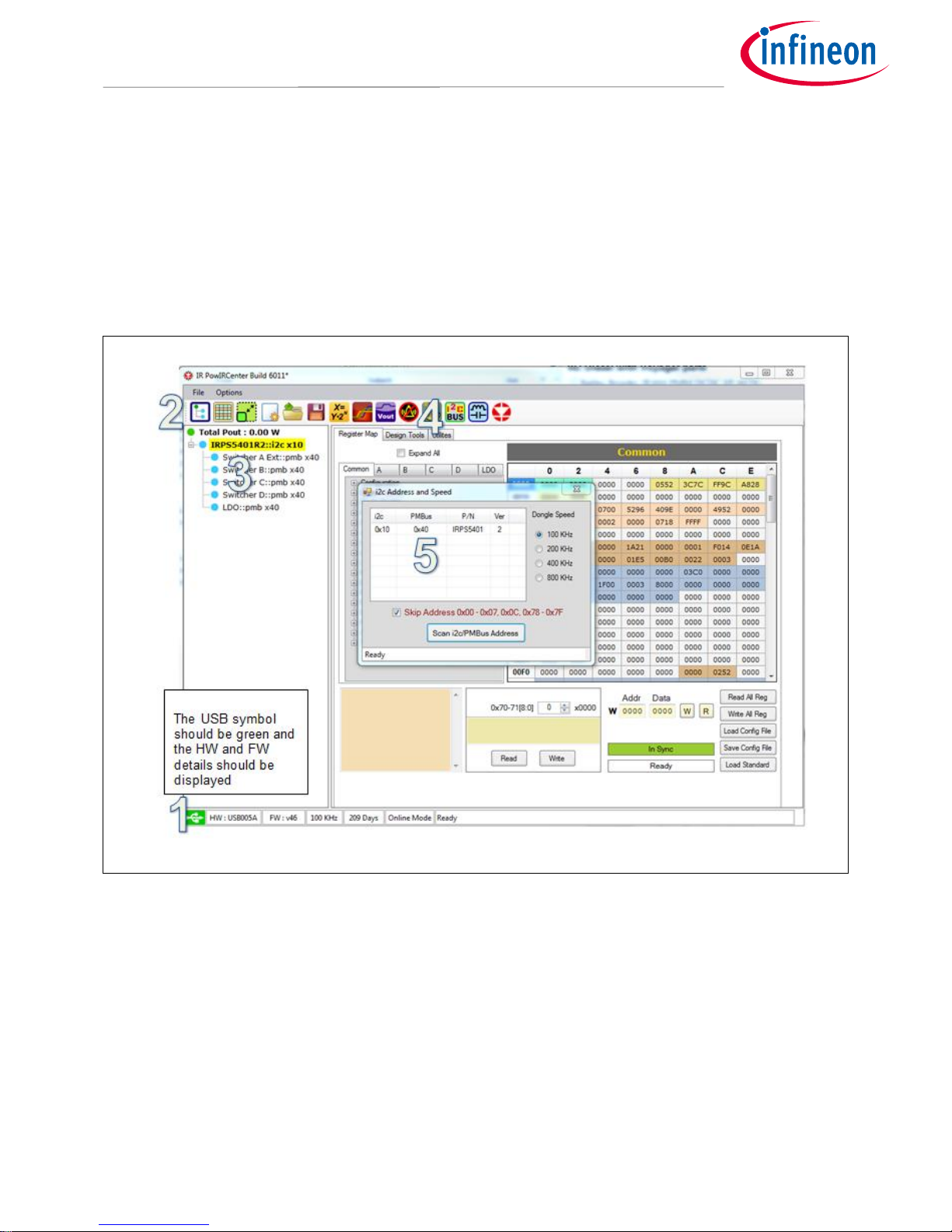
The IRPS5401 has 2 addresses; an I2C address for direct register read write access and a PMBus address for
sending PMBus commands. With the IRPS5401 powered up and the GUI communicating with the USB dongle
(1), you should be able to hit the Auto-populate button (2) and have the GUI recognize and populate the
IRPS5401 information (3). You can also use the address scan feature (4) to scan all addresses and see what
responds (5).
Figure 2 Example figure
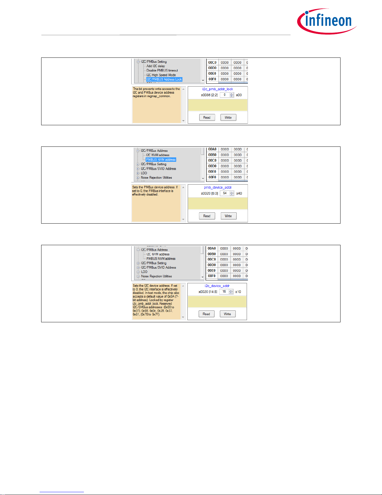
The base I2C and PMBus addresses are located in register 0x0020. The PMBus address bits are [6:0] and the I2C
address bits are [14:8]. Before these addresses can be updated, the register must be unlocked by setting REG
0x0086 bit [2] to 0. The PAGE command is used so that 1 common PMBus address can be used to access all 5
outputs.
Application Note 5 of 63 V 1.2
2018-12-12
5 Output PMIC Controller/ IRPS5401
User guide with DB295 and DB296 demo boards
Figure 3 Lock register
Figure 4 PMBus address
Figure 5 I2C address
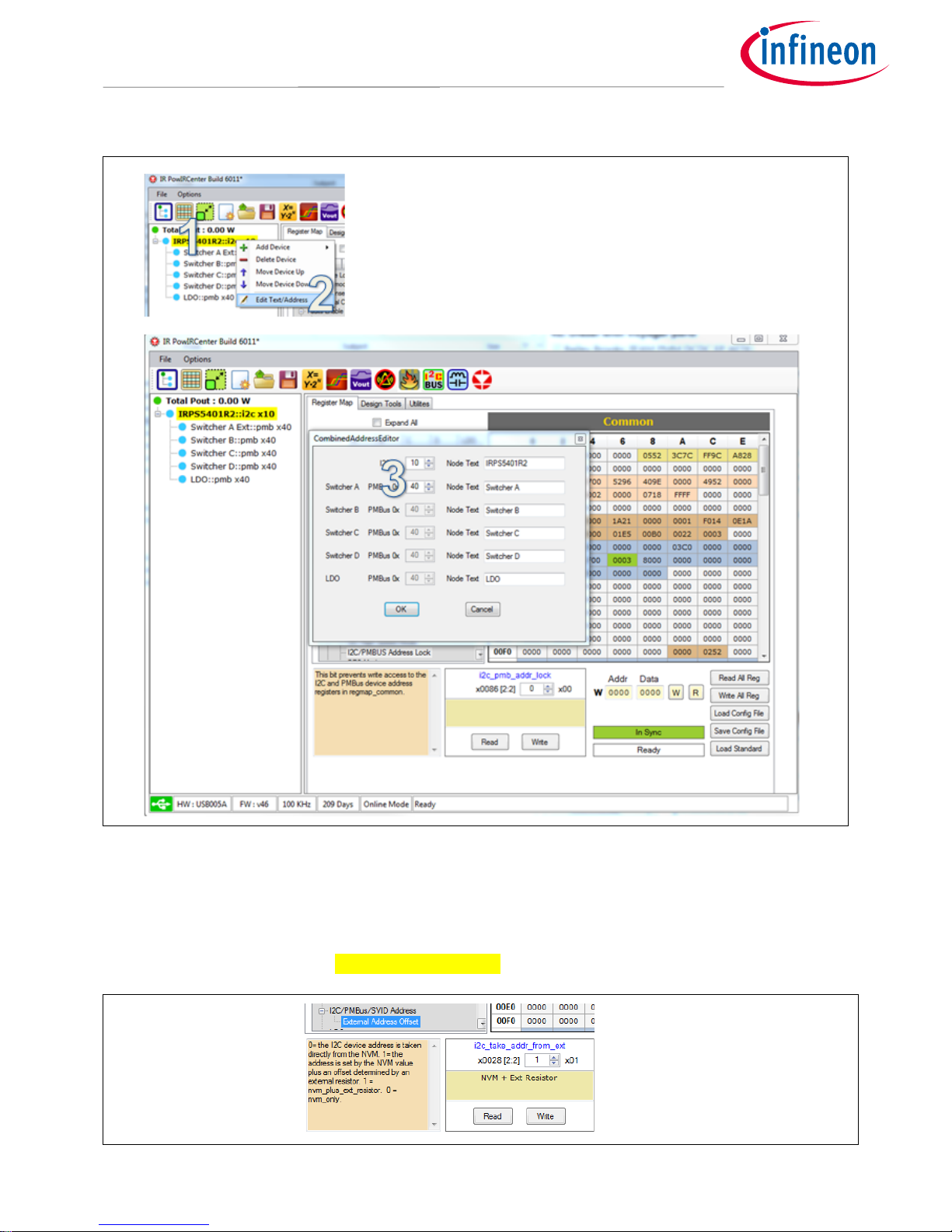
After the addresses have been updated in REG 0x0020, you will need to right click on the device (1) to bring up
the address editor dialog box (2) to update the addresses (3) that the GUI must use to communicate with the
IRPS5401 to the new values that where placed in REG 0x0020.
Application Note 6 of 63 V 1.2
2018-12-12
5 Output PMIC Controller/ IRPS5401
User guide with DB295 and DB296 demo boards
Figure 6 Example figure
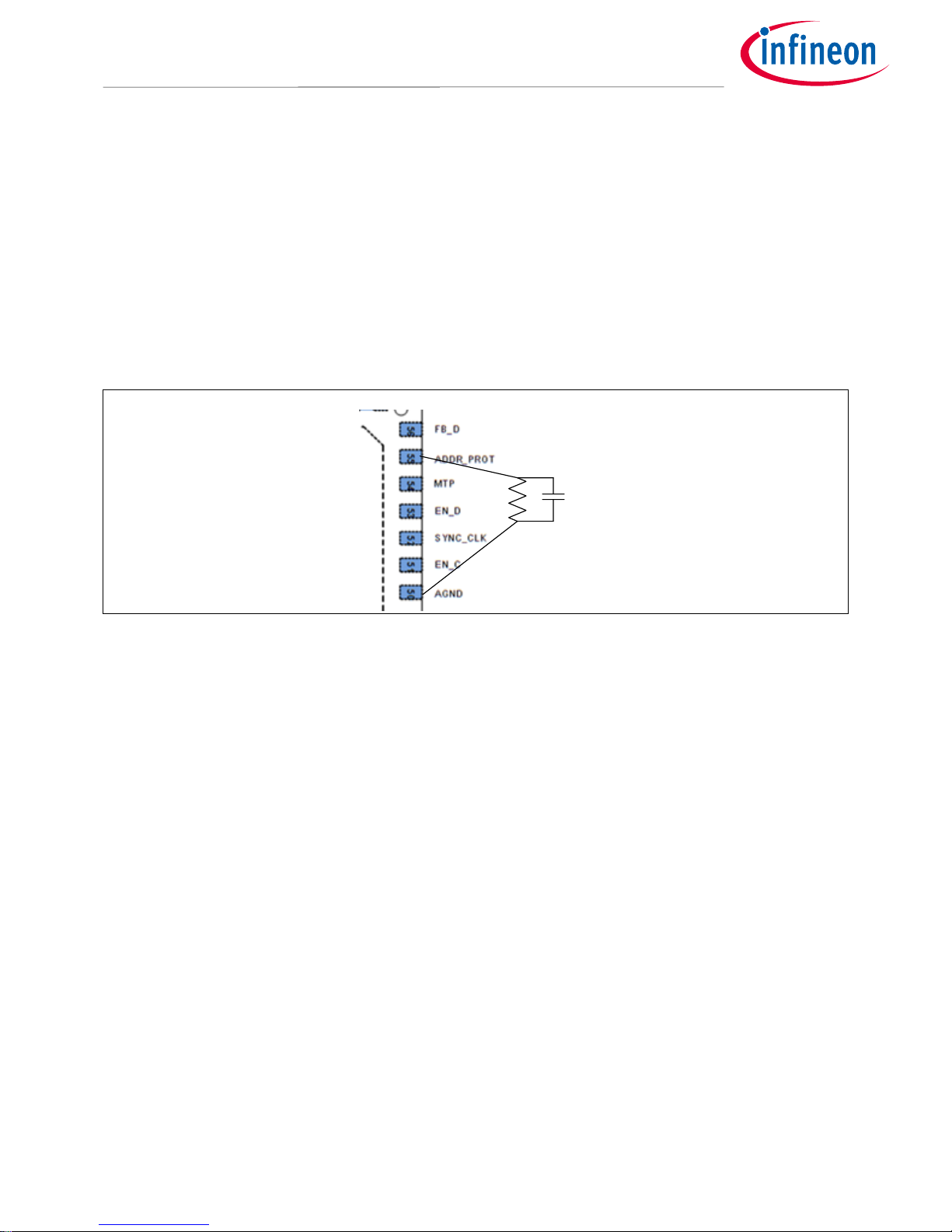
2.1 ADDR_PROT Pin
The base I2C and PMBus address that is placed in NVM can be offset by up to fifteen (15) so that up to sixteen
(16) IRPS5401 devices with a common NVM address can be placed on a common I2C/PMBus. This feature is
activated by setting 0x0028 bit [2], i2c_take_addr_from_ext, to 1. The part will ship from the factory with this
bit set to 1.
Application Note 7 of 63 V 1.2
2018-12-12
5 Output PMIC Controller/ IRPS5401
User guide with DB295 and DB296 demo boards
Figure 7 NVM address
With this bit set to 1, the device address will be the NVM address (in REG 0x0020) plus the offset added by the
resistor value attached to ADDR_PROT (pin 55).
The resistor must be connected from ADDR_PROT to AGND (pin 50). The resistor must be decoupled with a 10
nF capacitor (X7R type). The IRPS5401 will source 100 µA through the offset resistor for 1 ms immediately after
POR, the ADC will measure the voltage drop on the resistor and the value will be latched into the digital core.
This happens one time at start up, so updating this resistor after POR will not affect the offset.
Figure 8 Setting the resistor
This table shows the offset given for a specific resistor value. The I2C and PMBus address will be offset by the
same value.
**NOTE: the address can’t be offset above 7Fh. So, for instance, if you set the base address in NVM to 77h, the
largest offset resistor you can use is 5.49 K, +8 offset.
**NOTE: setting the PMBus address to 0 in NVM will disable PMBus
**NOTE: setting the I2C address to 0 in NVM will disable I2C communication
**NOTE: do not set the NVM (or NVM + offset) to these addresses; 01h to 07h, 0Ah or 0x0Ch
The IRPS5401 will be shipped from the factory with the I2C address defaulted to 10h and the PMBus address
defaulted to 40h. The address offset feature will be enabled. In order to see/use the address in NVM, you will
need to populate an 845 Ω resistor on pin 55. Do not leave pin 55 floating. Do not short pin 55 to GND. The
LSADC does not like trying to sense 0 V

Application Note 8 of 63 V 1.2
2018-12-12
5 Output PMIC Controller/ IRPS5401
User guide with DB295 and DB296 demo boards
Table 1 Address offset table
ADDR_PROT Resistor
Address Offset
0.845 kΩ
+0
1.30 kΩ
+1
1.78 kΩ
+2
2.32 kΩ
+3
2.87 kΩ
+4
3.48 kΩ
+5
4.12 kΩ
+6
4.75 kΩ
+7
5.49 kΩ
+8
6.19 kΩ
+9
6.98 kΩ
+10
7.87 kΩ
+11
8.87 kΩ
+12
10.00 kΩ
+13
11.00 kΩ
+14
12.10 kΩ
+15
2.2 TEST ADDRESS 0Ah
If the MTP pin (pin 54) is connected to VCC (or any voltage greater than 3.3 V) during POR, NVM will not load into
the working registers and the I2C address will be set to 0Ah regardless of the value in REG 0x0020 and the
address offset. This would be useful if you had 2 or more devices on the same bus that were responding to the
same address. You would be able to communicate with any individual device at address 0Ah by forcing the
MTP pin of that device high during POR.
Application Note 9 of 63 V 1.2
2018-12-12
5 Output PMIC Controller/ IRPS5401
User guide with DB295 and DB296 demo boards
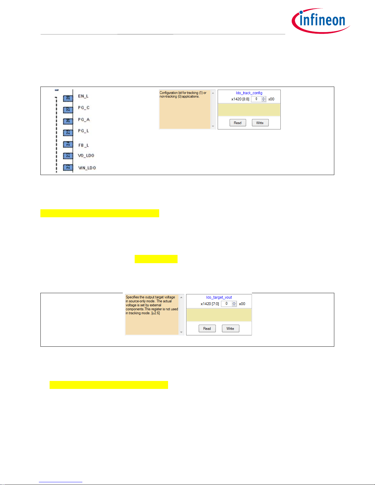
3 LDO Operation
The LDO input is pin 22. The input voltage has a range of 1.2 V to 5.5 V. The LDO output is pin 23.
Figure 9 LDO input
3.1 Source only mode
Set REG 0x1420 bit [8] (ldo_track_config) to 0
The LDO output has a range of 0.5 V to 3.6 V. The output is fed back to pin FB_L through a resistor divider
network. The output voltage will be set to (1+R_upper/R_lower)*0.5 V. With VOUT tied directly to FB_L, VOUT
will be set to 0.5 V…the reference voltage. The output is rated at 0.5 A. The OC_FAULT_LIMIT is read only and is
set to 0.72 A. The OV_WARN and FAULT, UV_WARN and FAULT are all read only and are a percentage of the
VOUT value set in REG 0x1420 [7:0] (ldo_target_vout). The lsb is 15.625 mV. So a value of 40h (1000/15.625 = 64
dec = 40h) would represent 1 V. Set this register to accurately represent the actual VOUT set by the external
components so that the UV and O V circuits trip at the correct value.
Figure 10 Source only mode
3.2 Sink/Source (Tracking) mode
Set REG 0x1420 bit [8] (ldo_track_config) to 1
In Tracking mode, VO_LDO must be connected directly to FB_L. An internal divider to VIN_LDO sets the
reference. The target VOUT is always ½*VIN_LDO so register ldo_target_vout has no function in tracking
mode. PMBus commands POWER_GOOD_ON and OFF also have no function in tracking mode. They are a
percentage of ½*VIN_LDO.

Application Note 10 of 63 V 1.2
2018-12-12
5 Output PMIC Controller/ IRPS5401
User guide with DB295 and DB296 demo boards
Figure 11 Tracking mode
3.3 Fault settings
All PMBus OV and UV CMD’s are READ ONLY for the LDO. A read command will report back the percentage of
VOUT shown in the table below. POWER_GOOD_ON and OFF is a read only command in tracking mode.
Table 2 Address offset table
MODE
Source Only
Tracking
Parameter
% of ldo_target_vout
% of ½*VIN_LDO
UV_FAULT
75
75
UV_WARN
87.5
87.5
OV_WARN
112.5
112.5
OV_FAULT
125
125
PG_ON
POWER_GOOD_ON
87.5
PG_OFF
POWER_GOOD_OFF
81.25
Application Note 11 of 63 V 1.2
2018-12-12
5 Output PMIC Controller/ IRPS5401
User guide with DB295 and DB296 demo boards
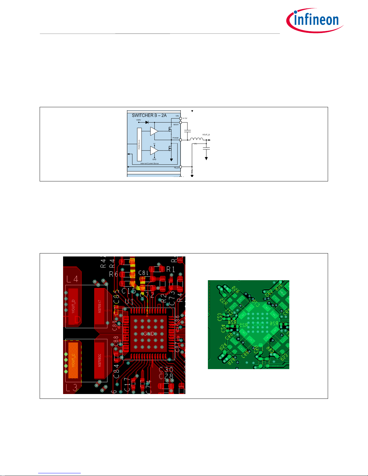
4 Switcher Operation
The IRPS5401 consists of 4 internal switching regulators (Switchers). SW-A and B are 2 A regulators. SW-C and
D are 4A regulators. SW-A can be configured to drive an external power stage such as the TDA21240
PowerStage or a discrete FET driver with power FET. This output can be designed to deliver up to 50 A. The
DB295 is configured such that SW-A is driving an external TDA21240 PowerStage.
Figure 12 Internal switching regulators
One of the most important considerations for the layout is the path length and loop area for the current path
from the input capacitors to the FET switches. C85 in the figure to the left is a 1 µF, 0402 multi-layer ceramic
capacitor (MLCC). It is one of the VIN decoupling caps for SW-D. It is placed adjacent to the VIN pins for SW-D
and is returned to GND through a via. On the bottom of the PCB, C70 and C71 are 10 µF MLCC caps that provide
additional decoupling for SW-D. They are arranged at 45° to provide the shortest path length to the GND RTN
vias under the IC.
Figure 13 Layout details
Other important considerations are:
The length and width of the copper connecting the SW Nodes to the inductors. They must be as short as
possible and as wide as possible, and be located only on the top layer

Application Note 12 of 63 V 1.2
2018-12-12
5 Output PMIC Controller/ IRPS5401
User guide with DB295 and DB296 demo boards
The 5x5 via pattern under the IRPS5401; these help transfer heat from the IC to the copper GND planes
on the PCB
Decouple VCC, MTP, and ADDR_PROT pins directly to AGND (pin 50) and tie AGND to GND with a
single point connection (see arrow above)
SW-A in external mode requires ISENSE and VSENSE lines to be routed back to the IC as differential
pairs
4.1 Setting the Switching Frequency
The phase angle between all switchers is maintained at a constant value. SW-A is at 0°, SW-C is at 90°, SW-B is
at 180° and SW-D is at 270°. A and B are 180° out of phase and C and D are 180° out of phase. In order to
accomplish this, all Switchers must operate at the same switching frequency (fsw). To that end, the fsw for all
switchers is controlled by the FREQUENCY_SWITCH PMBus command for SW-C.
SW-C will ACK any FREQUENCY_SWITCH command from 200 kHz to 2 MHz in increments of 1 kHz. Internally the
command is decoded and the actual FSW is set to the nearest value that can be supported with the 48 MHz
internal clock. For example, 500 kHz can be supported with ninety-six (96) 48 MHz clocks. So if you ask for 500
kHz, you get exactly 500 kHz. But if you wanted 450 kHz, the number of clocks required is 106.6667 (48/0.45). In
this case, the frequency would be set to one hundred and seven (107) 48 MHz clocks or 448.6 kHz. Fractional
values of 0.5 and above are rounded up to the next whole number.
FREQUENCY_SWITCH write commands to SW-A, B, and D will be ACK’d and ignored. FREQUENCY_SWITCH read
commands sent to SW-A, B, and D will read back the value sent in the ignored command.
SW-A FREQUENCY
The user can set the FSW of SW-A to be ½ of SW-C by sending a FREQUENCY_SWITCH command to SW-A
that is less than the FSW of SW-C. It does not have to be the value that is ½ of SW-C. Any FSW smaller
than SW-C FSW will result in SW-A FSW being set to ½ of SW-C. This ‘special’ ½ FSW ability only applies
to SW-A. Setting FSW for SW-A to ½ FSW of SW-C is usually done when SW-A is used in EXT driver mode.
FSW for SW-B and D will always be the same as SW-C
If the FSW of SW-C is less than 400 kHz, the FSW for SW-A will be the same as SW-C regardless of the FSW
setting of SW-A. The FSW of SW-A can’t be less than 200 kHz
SUMMARY
The FSW for all 4 switching regulators is controlled by SW-C. The FSW for SW-A may be set to ½ of SW-C
Because SW-C is the master, FREQUENCY_SWITCH ‘read’ commands to SW-A, B and D may not reflect the actual
FSW values for these outputs.
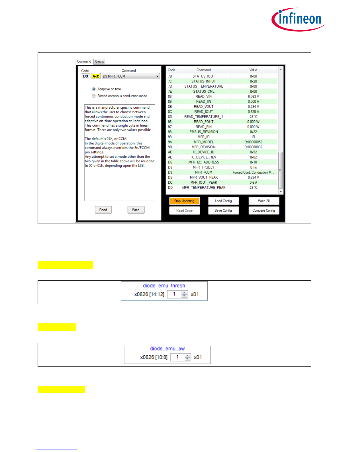
4.2 AOT Mode
Adaptive on-time (AOT) is a means of saving power at low output currents by reducing the switching frequency
and shutting off the LS FET before the inductor current goes negative. AOT mode is enabled by sending a MFR
specific PMBus command. Sending command D9h with a value 00h will enable AOT mode. AOT is sometimes
called discontinuous current mode (DCM) because the inductor current will go to 0 A.
In the GUI, select command D9h (MFR_FCCM), ‘Adaptive on-time’, then hit ‘write’ to switch between FCCM
(forced continuous conduction mode) and AOT. In AOT mode the switching frequency is a function of the load
so the enforced phase angle between outputs does not apply. As the load increases, the FSW will increase.
When the load is large enough to cause the FSW to be the same as the FSW set in FCCM, the switcher will
automatically switch to FCCM.
Application Note 13 of 63 V 1.2
2018-12-12
5 Output PMIC Controller/ IRPS5401
User guide with DB295 and DB296 demo boards
Figure 14 AOT mode
There are 4 configuration registers for each switcher that need to be set so that AOT mode operates correctly.
Diode_emu_threshold is the threshold below the DAC voltage that will cause the AOT pulse to start. This is
usually set to 1 3 mV:
Figure 15 Diode_emu_threshold
diode_emu_pw is the time that the HS FET is on after AOT is activated. It is usually set to 1. The on-time will be
a function of VIN. 1 = 180 ns at 12 V and 230 ns at 8 V:
Figure 16 Diode_emu_pw
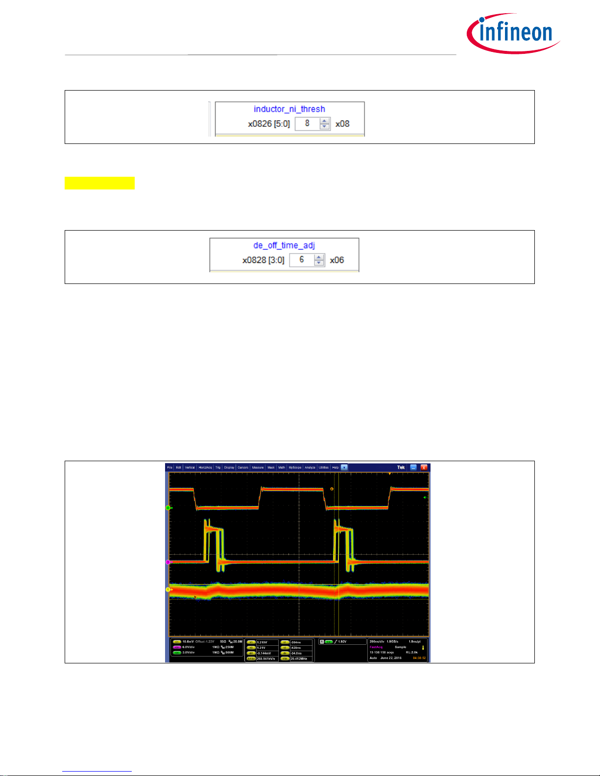
inductor_ni_thresh is the threshold that IOUT must be below before the output will try to enter into AOT mode.
If this is set to 0, the VR will never enter AOT mode even with the PMBUS command. 8 is a 0.25 A limit:
Application Note 14 of 63 V 1.2
2018-12-12
5 Output PMIC Controller/ IRPS5401
User guide with DB295 and DB296 demo boards
Figure 17 Inductor_ni_thresh
de_off_time_adj is an adjustment to the calculated LS FET on time. This prevents the inductor current from
going negative due to delays from the driver entering tri-state. Usually set to 6 400 nsec.
Figure 18 De_off_time_adj
**NOTE: IOUT reporting during AOT is not accurate. Do not send READ_IOUT commands while in AOT
Mode
4.3 External Sync
The IRPS5401 has a sync input (pin 52) that can be used to set the FSW to an external clock. The threshold
levels are LVTTL, 0.8V max for low and 2.1V min for high. The FSW setting for the IRPS5401 must be within a +/-
6.5% window of the desired sync frequency. The Sync input signal should be a 3.3V square wave with a 50%
duty cycle (+/- 10%)
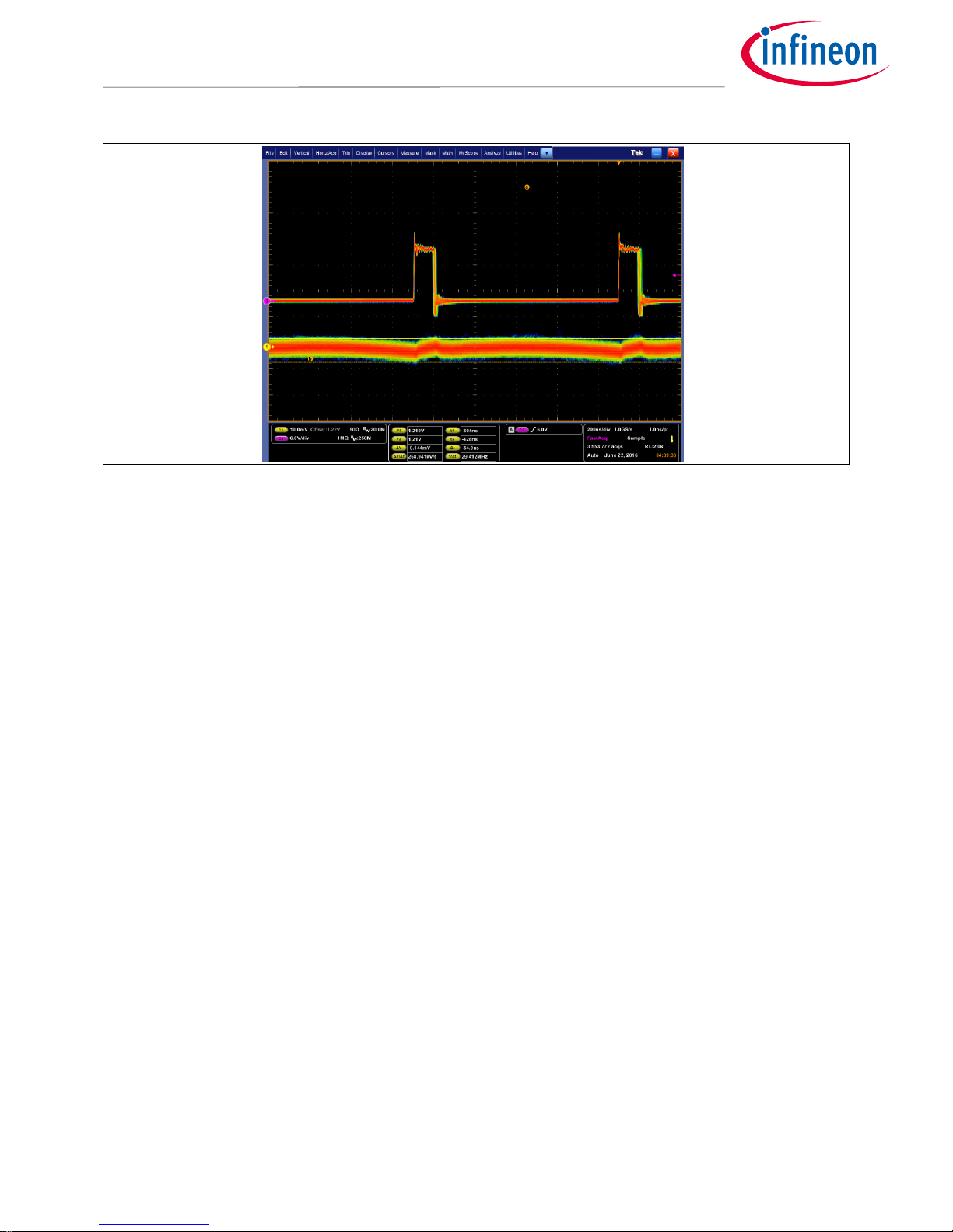
** NOTE: Using external sync will cause a ~40 nsec ‘jitter’ on the SW_NODE when compared to no sync input but
it is not reflected in the VOUT ripple. See comparison below
Figure 19 TOPSYNC in, MIDDLESW_NODE, BOTTOMRIPPLE
Application Note 15 of 63 V 1.2
2018-12-12
5 Output PMIC Controller/ IRPS5401
User guide with DB295 and DB296 demo boards
Figure 20 MIDDLESW_NODE, BOTTOMRIPPLE
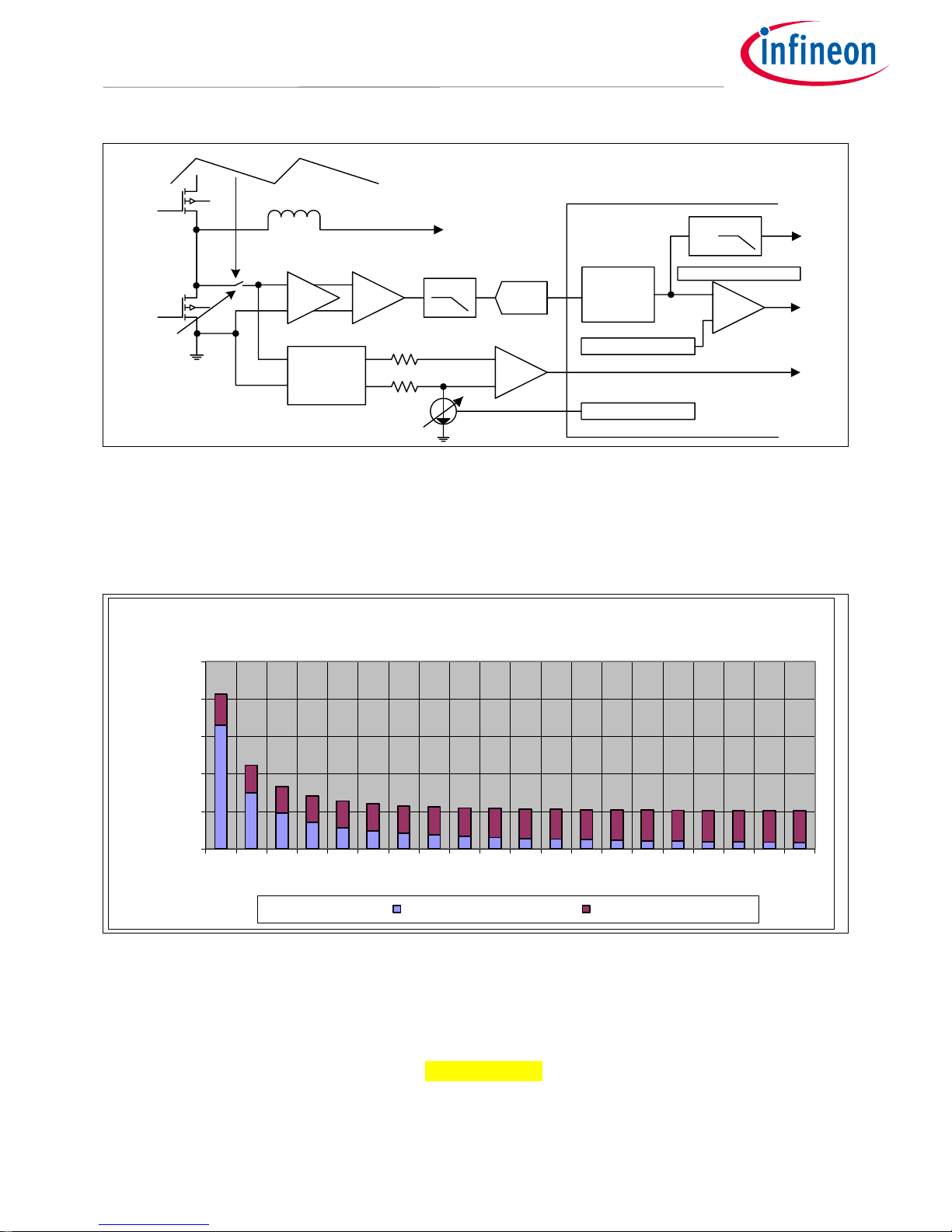
4.4 Current Sense and Over Current Settings
The 4 internal switchers sense IOUT by sensing the drop across the Rdson of the LS FET in the middle of the LS
FET conduction time. This gives the cleanest (least noisy) measurement because the SW_NODE has had time to
settle and stop ringing. Because the current is sensed in the middle of the LS FET on time (also the middle of
the inductor current down slope), the IRPS5401 senses the average output current, not the peak inductor
current.
The setting of the OC_WARN_LIMIT and OC_FAULT_LIMIT can be set to the DC value the user wants to see and
does not have to account for any added peak inductor current.
The OC_WARN_LIMIT is based on the output of the ADC and is filtered to 72 kHz. This digital current sense is
trimmed at ATE test to have a gain error of less than 5% and an offset error of less than 1% of the full load
capability.
The OC_FAULT_LIMIT is based on the output of a comparator that is looking directly at the Rdson. To ensure
OC_FAULT_LIMIT accuracy, the comparator is trimmed during ATE Test to tolerances of +/-10% at 3 A for the 2 A
outputs and +/-10% at 6 A for the 4 A outputs.
The PMBus commands OC_WARN_LIMIT and OC_FAULT_LIMIT have a range of 0 A to 15.97 A in increments of
31.25 mA. This means that the user can send a command and the IRPS5401 will ACK the command as valid.
However, the OC_FAULT_LIMIT is actually based on the comparator input which can only be set from 0 A to 4 A
in 0.25 A increments for the 2 A output and from 0 A to 8 A in 0.5 A increments for the 4 A outputs. (0 A to 16 A
for the combined C+D output) The internal logic will take the user’s commanded value and round it up to the
next real comparator setting. The OC_WARN_LIMIT is based on the ADC output so it really has 31.25 mA
increments. But it doesn’t make sense to set it above the OC_FAULT_LIMIT so it also has a practical limitation
of less than 15.97 A (except for the C+D application).
The user is encouraged to take into account the increase in inductor current that will occur during VOUT
increases. This capacitor charging current will have a magnitude of i= C_out*dv/dt and will be added to the DC
load current.
Application Note 16 of 63 V 1.2
2018-12-12
5 Output PMIC Controller/ IRPS5401
User guide with DB295 and DB296 demo boards
OCP LEVEL
SHIFT and
TEMP COMP
Control FET
Sync FET
Output Inductor
Inductor Current
To VOUT
Switch closes
and Rdson drop
is sampled in the
center of the
Sync FET
conduction time
72KHz
AAF
Telemetry
BW
isc_scale
TEMP COMP
VCC COMP
Digital Core
OC_FAULT_LIMIT
OCP Comparator
OC_WARN_LIMIT
To STATUS REG
READ_IOUT
3x
1.33,
1.66,
or 2
Set at
ATE trim
LSADC
ATE
Trimmed at
150% FL
OC WARN Comparator
To STATUS REG
and OCP
shutdown
Figure 21 Current settings
4.5 Current Reporting Accuracy
The internal switchers can have up to a 1% (of max rating) offset error in the IOUT sense. The gain error is ≤5%.
The chart below shows the % contribution for each source, offset and gain, from 5% load to 100% load for the 4
A outputs.
Figure 22 Current reporting
4.6 Over Voltage Settings at Start-up and Shut Down
Before the Switchers are enabled with the Enable pin or OPERATION command and during VOUT ramp up while
VOUT is less than 1 V, the output is protected from an OV condition by a fixed OVP threshold. The user can
choose between 1.35 V and 2.75 V by setting the fixed_ovp_thresh bit in register xx26h to 1 for 2.75 V, 0 for 1.35
V. If the output is using 2:1 scaling, the fixed thresholds will be 2x the values shown.
This bit is available for each switcher output.
0
5
10
15
20
25
0.2
0.4
0.6
0.8
1.0
1.2
1.4
1.6
1.8
2.0
2.2
2.4
2.6
2.8
3.0
3.2
3.4
3.6
3.8
4.0
Current Sense Error (%)
Load Current (A)
Current Sense Accuracy Error Contributions for 4A Outputs
Offset Gain
Application Note 17 of 63 V 1.2
2018-12-12
5 Output PMIC Controller/ IRPS5401
User guide with DB295 and DB296 demo boards
Set the fixed_ovp_thresh greater than the largest VOUT_COMMAND value that will be seen in the application.
The logic will switch from relative threshold to the fixed threshold when the Enable goes low, (or OPERATION
off command). If Enable goes low with VOUT > fixed_ovp_thresh, an OVP condition will be declared and VOUT
will be clamped low with the LS FET and the TOFF_RAMP down time will not be seen. The SM_ALERT# and the
STATUS bit will not assert because they are masked by the Enable pin = low.
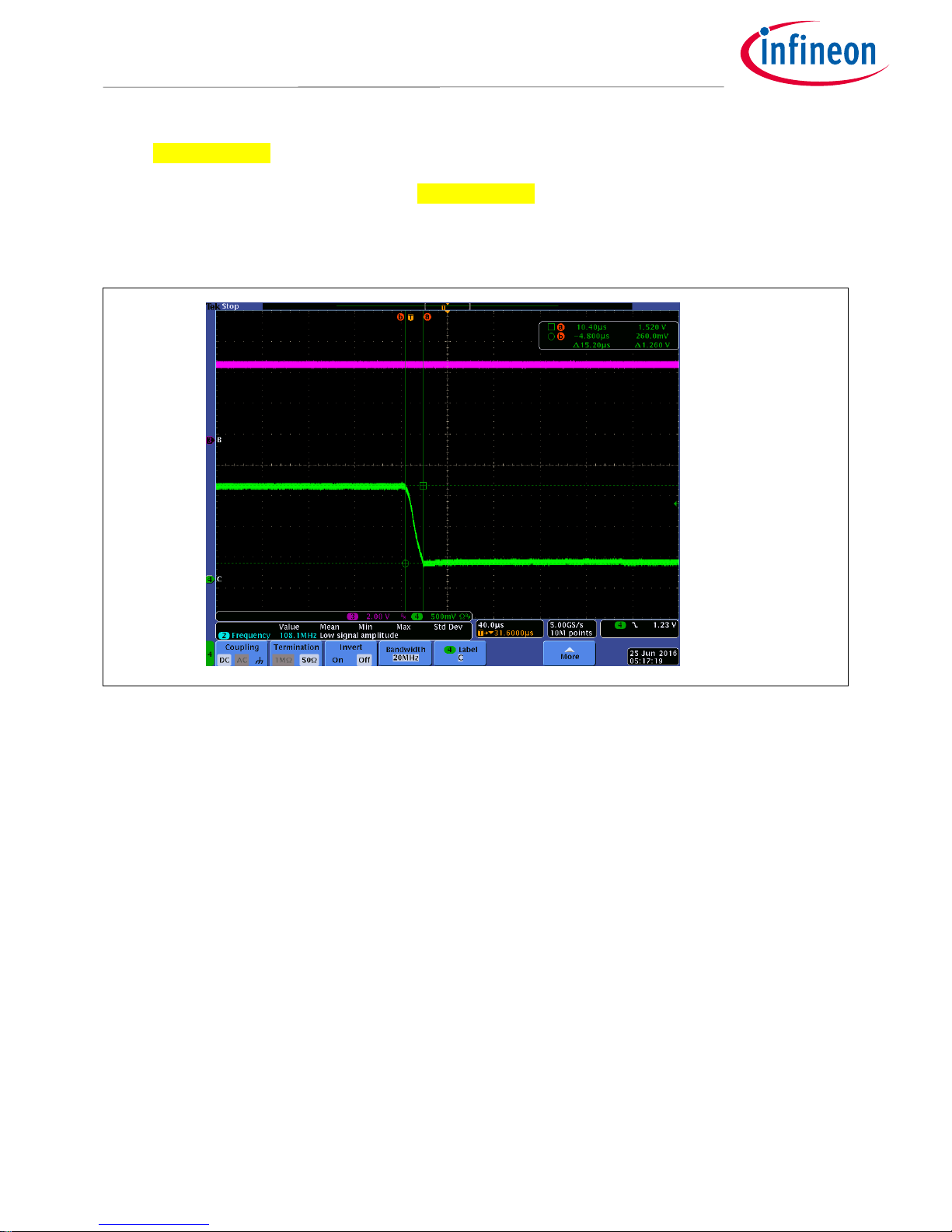
Figure 23 PINK=SM_ALERT#, GREEN=VOUT, After Enable is de-asserted, VOUT drops from 1.5 V to 0.27 V
in 15 µs TOFF_FALL is 1 ms, Fixed_OVP_Thresh=1.35 V, VOUT=1.5 V
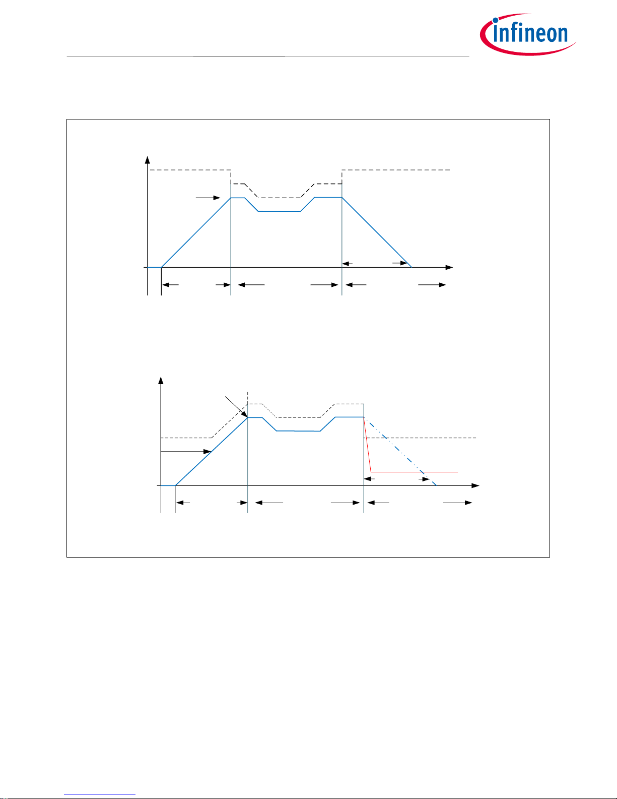
4.7 Over Voltage Settings under Steady State
After VOUT has ramped up past 1V (or after VOUT has reached its final value if it is less than 1 V), the OVP
switches to a value that is relative to the voltage set by VOUT_COMMAND. There are eight (8) relative threshold
values from 50mV to 400 mV (above VOUT) in 50 mV increments. The user sets the relative threshold by sending
a VOUT_OV_FAULT_LIMIT value that is greater than the VOUT_COMMAND by the required threshold. If the
VOUT_COMMAND is 1 V, a VOUT_OV_FAULT_LIMIT of 1.4 V (or greater) will cause the relative OVP threshold to
be 400 mV. If the VOUT_COMMAND is reduced to 0.9 V, the relative threshold of 400 mV will cause an OV fault at
1.3 V. If the VOUT_COMMAND increases VOUT to 1.2 V, the relative OVP threshold will be reduced to 200 mV
(FAULT_LIMIT-COMMAND). If the VOUT_COMMAND increases VOUT to 1.4 V, the new relative threshold will be
50 mV. The user can’t cause an OVP fault by setting the VOUT_COMMAND to a value greater than or equal to
the VOUT_OV_FAULT_LIMIT.
The relative OVP threshold will always be 50 mV above the VOUT_COMMAND value in the scenario described
above with the VOUT_COMMAND being increased to the VOUT_OV_FAULT_LIMIT or above.
The user should set the VOUT_OV_FAULT_LIMIT value such that it is > 400 mV above the largest
VOUT_COMMAND value that will be used in the application.
Each loop reports out the relative OVP threshold in Read Only (RO) register xx56h [2:0]. 0 = 50 mV, 1 = 100
mV…up to 7=400 mV. If 2:1 scaling is used, the relative OVP threshold is 2x the value shown.
Application Note 18 of 63 V 1.2
2018-12-12
5 Output PMIC Controller/ IRPS5401
User guide with DB295 and DB296 demo boards
The OV_WARN_LIMIT is not a relative threshold. It is the absolute value set by the user. The user can cause an
OV_WARN flag by sending a VOUT_COMMAND greater than the OV_WARN_LIMIT threshold.
Fixed_ovp_thresh
Relative OVP
threshold
Regulation
TON_RISE
Enable Low
VOUT_COMMAND < fixed_ovp_thresh
fixed_ovp_thresh
Enable Low
VOUT_COMMAND
TOFF_FALL
fixed_ovp_thresh
Relative OVP
threshold
RegulationTON_RISE
Enable Low
VOUT_COMMAND > fixed_ovp_thresh
fixed_ovp_thresh
Enable Low
VOUT_COMMAND
1V
TOFF_FALL
Expected VOUT
Actual VOUT due to OVP
OVP declared with
Enable Low
Figure 24 VOUT_COMMAND
If VOUT_COMMAND = 0 V (or any value less than 0.25 V), the relative o V threshold will be used as VOUT
transitions down to 0 V. Then the fixed_ovp_thresh is used while waiting for a new VOUT_COMMAND.
4.8 Under Voltage Settings
Similar to OVP, the UV protection is based on thresholds that are relative to the VOUT_COMMAND value. There
are eight (8) relative threshold values from 50 mV to 400 mV (below VOUT) in 50 mV increments. The user sets
the relative threshold by sending a VOUT_UV_FAULT_LIMIT value that is less than the VOUT_COMMAND by the
required threshold. If the VOUT_COMMAND is 1 V, a VOUT_UV_FAULT_LIMIT of 0.6 V (or less) will cause the
relative UVP threshold to be 400 mV. If the VOUT_COMMAND is increased to 1.2 V, the relative threshold of 400
mV will cause a UV fault at 0.8 V. If the VOUT_COMMAND decreases VOUT to 0.7 V, the relative UVP threshold
will be reduced to 100 mV (COMMAND-FAULT_LIMIT). If the VOUT_COMMAND decreases VOUT to 0.6 V (or
Application Note 19 of 63 V 1.2
2018-12-12
5 Output PMIC Controller/ IRPS5401
User guide with DB295 and DB296 demo boards
lower), the new relative threshold will be 50 mV. The user can’t cause a UVP fault by setting the
VOUT_COMMAND to a value less than or equal to the VOUT_UV_FAULT_LIMIT.
The relative UVP threshold will always be 50 mV below the VOUT_COMMAND value in the scenario described
above with the VOUT_COMMAND being decreased to the VOUT_UV_FAULT_LIMIT or below.
The user should set the VOUT_UV_FAULT_LIMIT value such that it is < 400 mV below the smallest
VOUT_COMMAND value that will be used in the application.
Each loop reports out the relative UVP threshold in Read Only (RO) register xx56h [6:4]. 0 = 50 mV, 1 = 100 mV …
up to 7=400 mV. If 1:2 scaling is used, the relative UVP threshold is 2x the value shown.
The UV_WARN_LIMIT is not a relative threshold. It is the absolute value set by the user. The user can cause a
UV_WARN flag by sending a VOUT_COMMAND less than the UV_WARN_LIMIT.
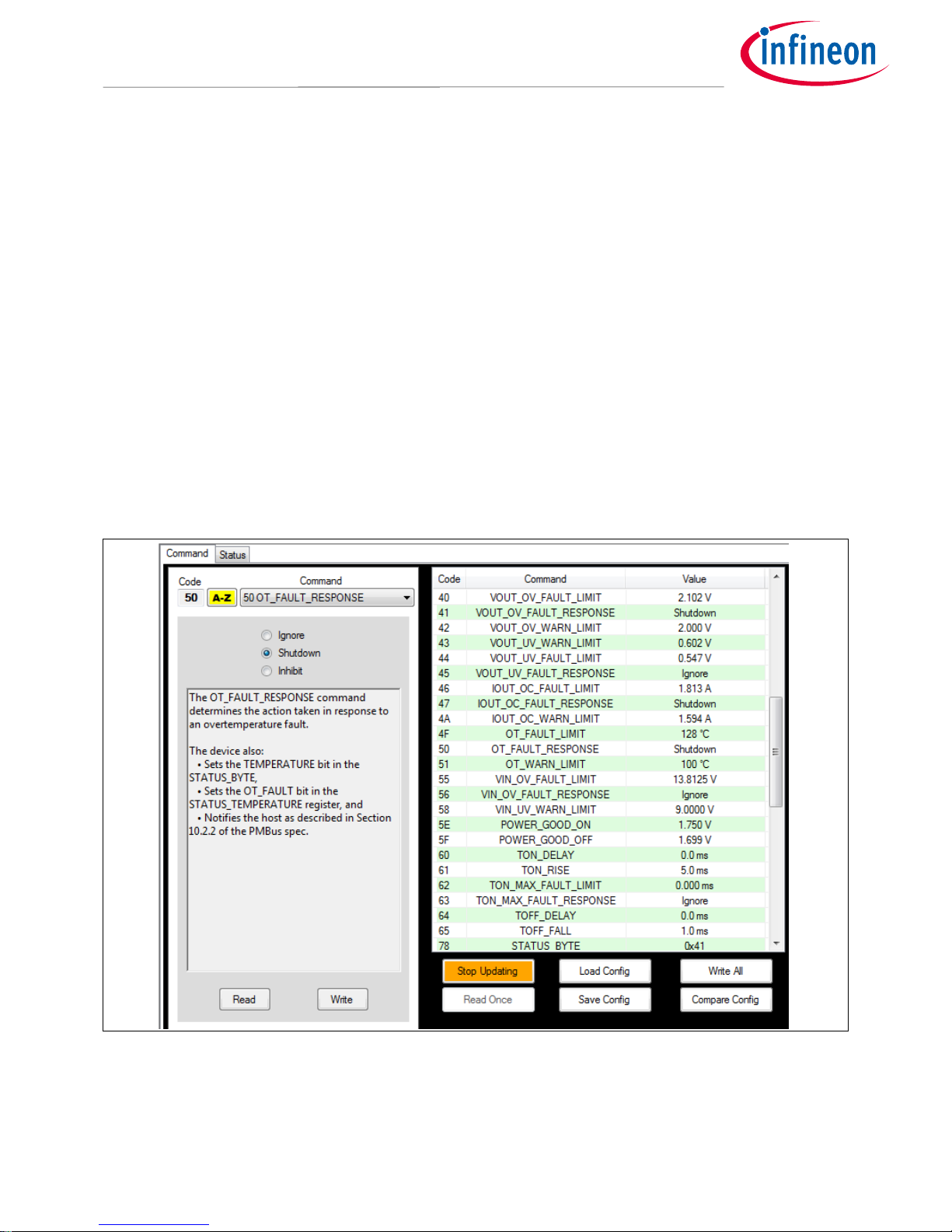
4.9 Over Temperature
The IRPS5401 has two (2) on die temp sensors; one for SW-A and B and one for SW-C, D and the LDO.
A READ_TEMPERATURE_1 command to SW-A or SW-B will report the same value. A READ_TEMPERATURE_1
command to SW-C, D or the LDO will report the same value.
The OT_WARN_LIMIT and OT_FAULT_LIMIT can be set to any value from 0°C to 255°C in increments of 1°C.
OT_WARN should be set less than OT_FAULT.
The OT_FAULT_RESPONSE can be set to IGNORE, SHUTDOWN and latch off, or SHUTDOWN and auto recover
when temp decreases (also known as INHIBIT).
Figure 25 Command set
 Loading...