

Page 1

AN2018
-
13
IM393 Application note
IM393 IPM Technical Description
About this document
Scope and purpose
The scope of this application note is to describe the IM393 product family and the basic requirements for
operating the products in a recommended mode. This includes integrated components, such as IGBT,
bootstrap functionality or gate drive IC, as well as the design of the necessary external circuitry, interfacing and
application use.
Intended audience
Power electronics engineers who want to design reliable and efficient motor drive application with IM393 IPM
family.
Table of contents
About this document ....................................................................................................................... 1
Table of contents ............................................................................................................................ 1
1 Introduction .......................................................................................................................... 3
1.1 Product line-up ........................................................................................................................................ 4
1.2 Nomenclature .......................................................................................................................................... 5
2 Internal components and package technology .......................................................................... 6
2.1 Power transistor and diode technology ................................................................................................. 6
2.2 Control IC – Six-channel gate driver IC ................................................................................................... 6
2.3 Thermistor ............................................................................................................................................... 7
2.4 Package technology ................................................................................................................................ 8
3 Product overview and pin description ...................................................................................... 9
3.1 Internal circuit and features ................................................................................................................... 9
3.2 Maximum electrical rating .................................................................................................................... 10
3.3 Description of the input and output pins ............................................................................................. 10
3.4 Outline drawings ................................................................................................................................... 15
4 Interface circuit and layout guide ........................................................................................... 17
4.1 Input/output signal connection ............................................................................................................ 17
4.2 Input/output signal connection ............................................................................................................ 19
4.3 Recommended circuit current of power supply .................................................................................. 20
4.4 Recommended layout for over-current protection (OCP) and short-circuit protection (SCP)
functions ................................................................................................................................................ 21
4.5 Recommended wiring of shunt resistor and snubber capacitor ......................................................... 21
4.6 Pin and screw hole coordinates for IM393-XX footprint ...................................................................... 23
5 Function and protection circuit ............................................................................................... 25
5.1 Over-current protection ........................................................................................................................ 25
5.1.1 Timing chart of over-current protection (OCP) ............................................................................... 25
5.1.2 Selecting current-sensing shunt resistor ........................................................................................ 26
5.1.3 Delay time ......................................................................................................................................... 27
Application Note Please read the Important Notice and Warnings at the end of this document V 1.0
www.infineon.com page 1 of 53 2019-04-01
Page 2

IM393 Application note
IM393 IPM Technical Description
Introduction
5.2 Fault output and auto-clear function ................................................................................................... 27
5.3 Undervoltage lockout (UVLO) ............................................................................................................... 29
5.4 Over-temperature protection ............................................................................................................... 31
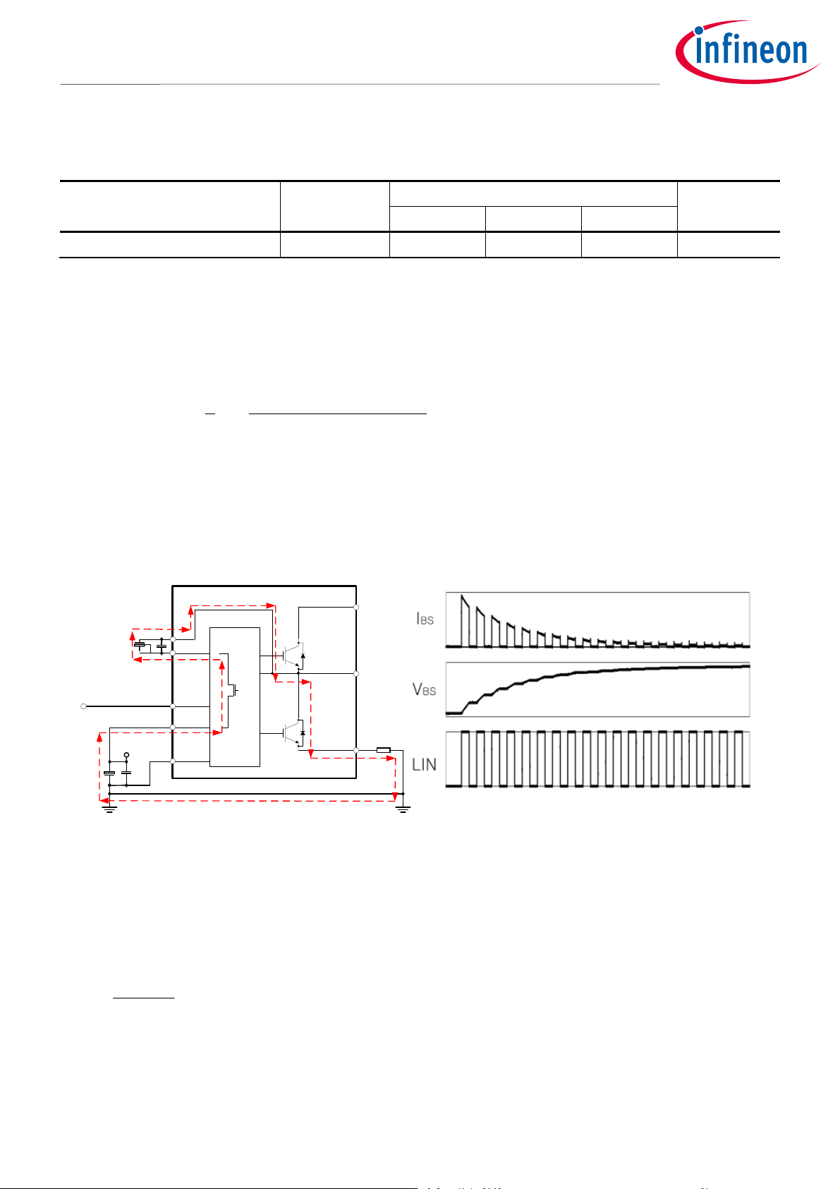
6 Bootstrap circuit ................................................................................................................... 33
6.1 Bootstrap circuit operation .................................................................................................................. 33
6.2 Initial charge of bootstrap capacitor .................................................................................................... 34
6.3 Bootstrap capacitor selection .............................................................................................................. 34
6.4 Charging and discharging of the bootstrap capacitor during PWM inverter operation ..................... 35
7 Thermal design ..................................................................................................................... 37
7.1 Introduction ........................................................................................................................................... 37
7.2 Power losses .......................................................................................................................................... 38
7.2.1 Conduction losses ............................................................................................................................ 38
7.2.2 Switching losses ............................................................................................................................... 39
7.3 Thermal impedance .............................................................................................................................. 39
7.4 Temperature rise considerations and calculation example ................................................................ 40
7.5 Heat sink selection guide ...................................................................................................................... 42
7.5.1 Required heat sink performance ..................................................................................................... 42
7.5.2 Heat sink characteristics .................................................................................................................. 43
7.5.2.1 Heat transfer from heat source to heat sink .............................................................................. 43
7.5.2.2 Heat transfer within the heat sink .............................................................................................. 43
7.5.2.3 Heat transfer from heat sink surface to ambient ....................................................................... 43
7.5.3 Selecting a heat sink ........................................................................................................................ 45
7.6 Online simulation tool .......................................................................................................................... 45
8 Heat sink mounting and handling guidelines ............................................................................ 47
8.1 Heat sink mounting ............................................................................................................................... 47
8.1.1 General guidelines ........................................................................................................................... 47
8.1.1.1 Recommended tightening torque .............................................................................................. 47
8.1.1.2 Screw tightening to heat sink ..................................................................................................... 48
8.2 Handling guideline ................................................................................................................................ 49
8.3 Storage guideline .................................................................................................................................. 50
8.3.1 Recommended storage conditions ................................................................................................. 50
9 References ........................................................................................................................... 51
Revision history............................................................................................................................. 52
Application Note 2 of 53 V 1.0
2019-04-01
Page 3

IM393 Application note
IM393 IPM Technical Description
Introduction
1 Introduction
With the global emphasis on energy efficiency, there are ever stricter requirements on the efficiency of motor
drive circuits. CIPOS™ Integrated Power Modules (IPMs) are becoming more popular in the home appliance and
industrial motor-drive applications, because of their higher efficiency, smaller size, easier assembly and shorter
development time.
The next generation of CIPOS™ IPM from Infineon Technologies has been developed with a focus on improving
module efficiency and long-term reliability. The combined benefits of advanced trench IGBT technology and
optimized package design have enabled us to achieve higher efficiency and improved reliability, along with
minimized module system costs. Integrating discrete power semiconductors and drivers into one package
allows designers to reduce the time and effort spent on design. To meet the strong demand for small size and
higher power density, Infineon has developed a new family of highly integrated intelligent power modules that
contain nearly all of the semiconductor components required to drive electronically controlled variable-speed
electric motors.
This advanced IPM is a combination of Infineon’s newest low V
best trade-off between conduction and switching losses, and the industry benchmark three-phase high voltage,
high-speed driver (3.3 V-compatible) in a fully isolated thermally enhanced package. A built-in high precision
temperature monitor and over-current protection feature, along with the short-circuit rated IGBTs and
integrated undervoltage lockout function, deliver a high level of protection and fail-safe operation. Using a dual
or single in-line package with full transfer molded structure resolves the isolation problem to the heat sink.
The application note concerns the following products:
− IM393-S6E
− IM393-S6F
− IM393-M6E
− IM393-M6F
− IM393-L6E
− IM393-L6F
− IM393-X6E
− IM393-X6F
IM393-XX is part of CIPOS™ Tiny family of intelligent power modules which are designed for motor drives in
household appliances covering a wide range of power from 100 W up to 1500 W with products such as:
− Washing machines
− Dish washers
− Refrigerators
− Air conditioning compressors
− Pumps
trench IGBT technology optimized for the
CE(ON)
Application Note 3 of 53 V 1.0
2019-04-01
Page 4

IM393 Application note
IM393 IPM Technical Description
Introduction
1.1 Product line-up
Table 1 IM393-XX Products
Rating
Part Number
Current
(A)
Voltage
(V)
Internal
Circuit
Package
Isolation
voltage (V
RMS
Main applications
)
Refrigerator
IM393-S6E(F) 6 A
E(Fully
Dryer
Dish washer
molded
Washing
machine
Dryer
Elevator door
Washing
machine
Air conditioner
Elevator door
IM393-M6E(F) 10 A
IM393-L6E(F) 15 A
600 V
3 ф Bridge
Open
emitter
DIP
Module)
F(Fully
molded
SIP
Module)
2000 V
RMS
sinusoidal,
1min.
IM393-X6E(F) 20 A Air conditioner
Fan
Pump
GPI
Application Note 4 of 53 V 1.0
2019-04-01
Page 5

IM393 Application note
IM393 IPM Technical Description
Introduction
1.2 Nomenclature
Application Note 5 of 53 V 1.0
2019-04-01
Page 6

IM393 Application note
IM393 IPM Technical Description
Internal components and package technology
2 Internal components and package technology
2.1 Power transistor and diode technology
IM393-XX IPM products are based on new Infineon IGBT6 TRENCHSTOP™ technology [1]. This new IGBT
generation is based on trench and field-stop technology, and offers significant improvements in terms of loss
reduction. It features the well-known properties of robustness of Infineon’s IGBT, including short-circuitwithstand capability and maximum-junction temperature. Moreover, all the advantages of this technology are
maintained in order to achieve the highest efficiency and power density. The features include very low static
parameters such as the saturation voltage of the IGBT or the forward voltage of the diode. Excellent dynamic
parameters such as turn-off energy of the IGBT or the reverse-recovery charge of the diode are also valuable
features. The forward diodes are ultrafast with very soft recovery characteristics that lead to a reduction in
reverse-recovery and turn-on energy losses.
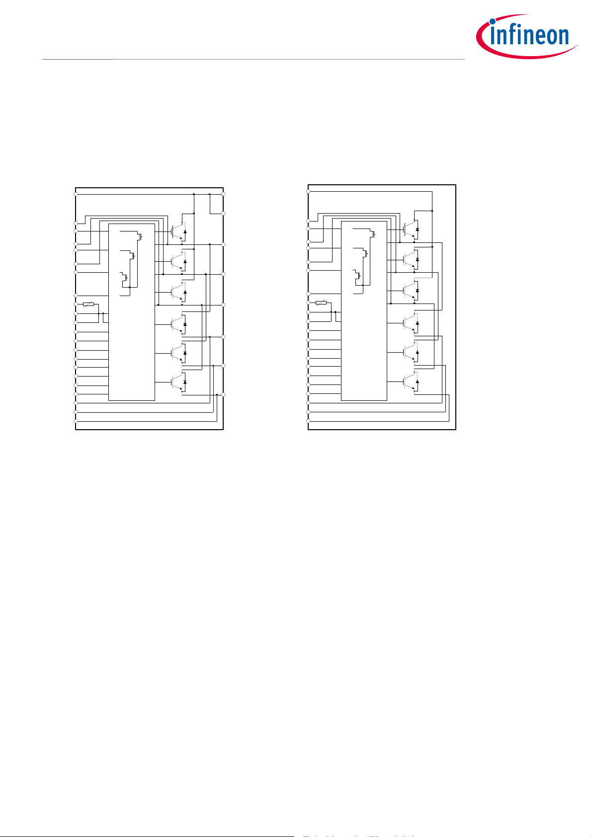
2.2 Control IC – Six-channel gate driver IC
The driver is a high-voltage, high-speed IGBT gate driver with three high-side and three low-side referenced
output channels for three-phase applications. The IC is designed to be used with low-cost bootstrap power
supplies. The bootstrap diode functionality has been integrated into this device to reduce the component
count on the PCB. Proprietary HVIC and latch-up immune CMOS technologies have been implemented in a
rugged monolithic structure. The floating logic input is compatible with standard CMOS and LSTTL output
(down to 3.3 V logic). A current-trip function which terminates all six outputs can be done by an external current
sense resistor. Enable functionality is available to terminate all six outputs simultaneously. An open-drain
FAULT signal is provided to indicate that a fault has occurred. Fault conditions are cleared automatically after a
delay programmed externally via an RC network connected to the RCIN input. The output drivers feature a
high-pulse current buffer stage designed for minimum driver cross conduction. Shoot-through protection
circuitry and a minimum dead-time circuitry have been integrated into this IC. Propagation delays are matched
to simplify the HVIC’s use in high-frequency applications.
The HVIC technology uses proprietary monolithic structures integrating bipolar, CMOS and lateral DMOS
devices [2]. Using this mixed-signal HVIC technology, both high-voltage, level-shifting circuits, and low-voltage
analog and digital circuits can be implemented. This technology places high-voltage circuits in a ‘well’ formed
by polysilicon rings which can float 600 V within the same silicon, away from the low-voltage circuitry, as shown
in Figure 1.
These HVIC gate drivers with floating switches are well-suited for topologies requiring high-side and bridge
configuration.
Figure 1 Structure and cross section of the HVIC
Application Note 6 of 53 V 1.0
2019-04-01
Page 7

IM393 Application note
IM393 IPM Technical Description
Internal components and package technology
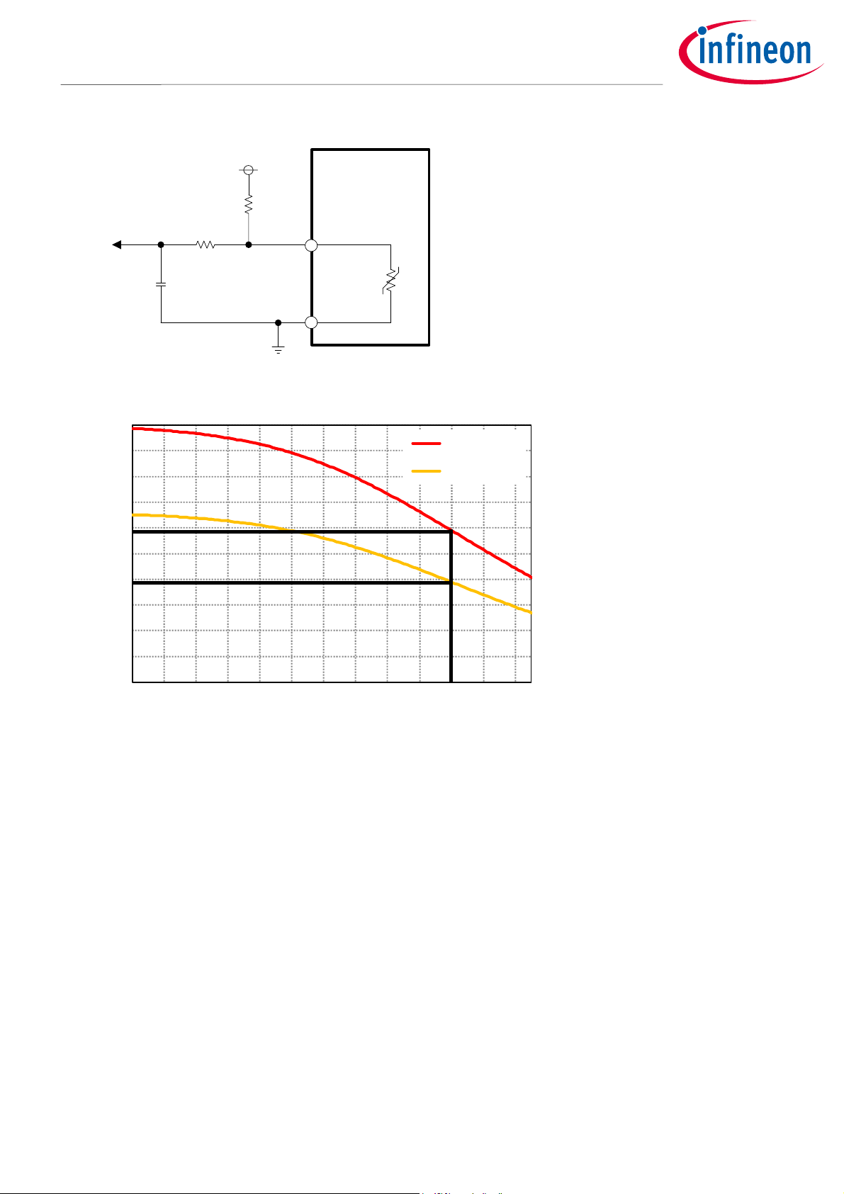
2.3 Thermistor
All IM393-XX IPMs have internal thermistors to sense the module temperature. Figure 2 shows the correlation
between NTC temperature (TTH) and the thermistor output voltage which can be used to set the threshold for
over-temperature protection.
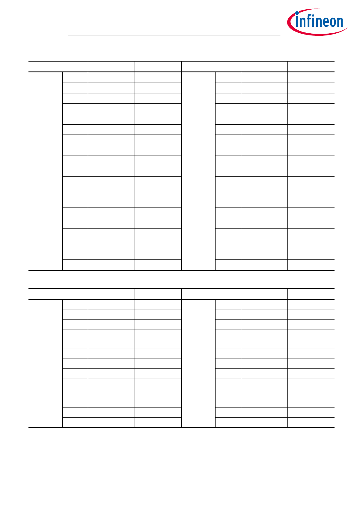
Table 2 Raw data of the thermistor used in IM393-XX
T [℃] R
[kΩ] R
min
[kΩ] R
typ
max
[kΩ]
Tol [%]
T [℃] R
[kΩ] R
min
[kΩ] R
typ
max
[kΩ]
Tol [%]
-40 1438.40 1568.15 1705.34 8.7% 45 18.930 20.097 21.282 5.9%
-35 1040.65 1130.82 1225.73 8.4% 50 15.448 16.432 17.436 6.1%
-30 761.64 825.03 891.47 8.1% 55 12.695 13.531 14.385 6.3%
-25 563.53 608.58 655.58 7.7% 60 10.4830 11.1942 11.9238 6.5%
-20 421.23 453.57 487.16 7.4% 65 8.6961 9.3033 9.9279 6.7%
-15 317.53 340.93 365.14 7.1% 70 7.2454 7.7652 8.3016 6.9%
-10 241.62 258.72 276.33 6.8% 75 6.0619 6.5084 6.9703 7.1%
-5 185.51 198.10 211.02 6.5% 80 5.0922 5.4767 5.8755 7.3%
0 143.62 152.98 162.53 6.2% 85 4.3017 4.6342 4.9800 7.5%
5 112.35 119.37 126.51 6.0% 90 3.6482 3.9366 4.2372 7.6%
10 88.440 93.740 99.109 5.7% 95 3.1056 3.3565 3.6186 7.8%
15 70.033 74.055 78.112 5.5% 100 2.6533 2.8721 3.1012 8.0%
20 55.770 58.837 61.918 5.2% 105 2.2748 2.4661 2.6669 8.1%
25 44.650 47.000 49.350 5.0% 110 1.9567 2.1245 2.3009 8.3%
30 35.772 37.737 39.711 5.2% 115 1.6886 1.8360 1.9913 8.5%
35 28.801 30.449 32.110 5.5% 120 1.4616 1.5915 1.7287 8.6%
40 23.298 24.682 26.084 5.7% 125 1.2690 1.3837 1.5050 8.8%
Thermistor temperature (or voltage reading) can then be linked to the IGBT junction temperature. The VTH can
be used as a microcontroller input to monitor IGBT junction temperature during operation.
Figure 2 IGBT junction temperature vs. internal thermistor temperature for IM393-L6E
Application Note 7 of 53 V 1.0
2019-04-01
Page 8

IM393 Application note
IM393 IPM Technical Description
Internal components and package technology
Figure 2 is valid only for the following conditions:
- V
= 300 V
DC
- PWM sinusoidal modulation
- I
- F
- F
phase = 5 A
rms
= 16 kHz
sw
= 50 Hz
mod
- MI = 0.8
- PF = 0.6
- Heat sink R
For different application conditions, the difference between TJ and T
less heat. Also in the extreme case of zero current, TJ and T
= 1.25 °C/W
th
will be smaller if the module dissipates
TH
will be identical. In any case, it should be ensured
TH
for safety reasons that the absolute maximum junction temperature is not reached.
Please note that an over-temperature event in the IGBT will only be visible in the NTC readings after a certain
time, which depends significantly on the application conditions.
2.4 Package technology
IM393-XX offers the smallest size while providing high-power density up to 600 V and 20 A by employing
TRENCHSTOP™ IGBT and emitter-controlled diodes with a six-channel gate drive IC. It contains all power
components such as IGBTs, and isolates them from each other and from the heat sink. All low-power
components such as the gate drive IC and thermistor are assembled on a lead frame.
The electric insulation is provided by the mold compound, which is simultaneously the thermal contact to the
heat sink. In order to further decrease the thermal impedance, the internal lead-frame design has been
optimized [3]. Figure 3 shows the external view of the IM393-XX package.
(a) Dual in-line package (b) Single in-line package
Figure 3 External view of IM393-XX
Application Note 8 of 53 V 1.0
2019-04-01
Page 9
IM393 Application note
IM393 IPM Technical Description
Product overview and pin description
3 Product overview and pin description
3.1 Internal circuit and features
Figure 3 illustrates the internal block diagram of the IM393-XX. It consists of a three-phase IGBT inverter circuit
and a driver IC with control functions. The detailed features and integrated functions of IM393-XX are described
as follows:
(1) P
(35) P
(1) P
(3) VS(W)
(4) VB(W)
(6) VS(V)
(7) VB(V)
(9) VS(U)
(10) VB(U)
(12) VDD
(13) VTH
(14) COM
(15) COM
(16) ITRIP
(17) RFE
(18) HIN(U)
(19) HIN(V)
(20) HIN(W)
(21) LIN(U)
(22) LIN(V)
(23) LIN(W)
(24) N(W)
(25) N(V)
(26) N(U)
(33) P
VB3
VB2
VB1
VDD
-t°
COM
VSS
ITRIP
RFE
HIN1
HIN2
HIN3
LIN1
LIN2
LIN3
HO3
HO2
HO1
VS3
VS2
VS1
LO3
LO2
LO1
(32) W
(31) V
(30) U
(29) N(W)
(28) N(V)
(27) N(U)
(3) VS(W)
(4) VB(W)
(6) VS(V)
(7) VB(V)
(9) VS(U)
(10) VB(U)
(12) VDD
(13) VTH
(14) COM
(15) COM
(16) ITRIP
(17) RFE
(18) HIN(U)
(19) HIN(V)
(20) HIN(W)
(21) LIN(U)
(22) LIN(V)
(23) LIN(W)
(24) N(W)
(25) N(V)
(26) N(U)
VB3
VB2
VB1
VDD
-t°
COM
VSS
ITRIP
RFE
HIN1
HIN2
HIN3
LIN1
LIN2
LIN3
HO3
VS3
HO2
VS2
HO1
VS1
LO3
LO2
LO1
(a) Dual in-line package (b) Single in-line package
Figure 4 Internal circuit
Features
− 600 V / 6 A to 20 A rating in one physical package size (mechanical layouts are identical)
− Motor power range from 100 W to 1.5 kW
− Fully isolated dual in-line package (DIP) and single in-line package (SIP) molded module
− Infineon low- V
− Undervoltage lockout for all channels
− Rugged gate driver technology with stability against transients and negative voltage
− Integrated bootstrap functionality
− Matched delay times of all channels / Built-in deadtime
− Over-current protection
− Lead-free terminal plating; RoHS-compliant
− 3.3 V Schmitt triggered input logic
− Cross conduction preventing logic
− Low-side emitter pins accessible for current monitoring
− Active high input signal logic
− Isolation 2000 V
− High operating case temperature, T
− Temperature monitor
TRENCHSTOP™ IGBTs with separate freewheeling diode
CE(ON)
min and CTI>600
RMS
= 125°C
Cmax
Application Note 9 of 53 V 1.0
2019-04-01
Page 10

IM393 Application note
IM393 IPM Technical Description
Product overview and pin description
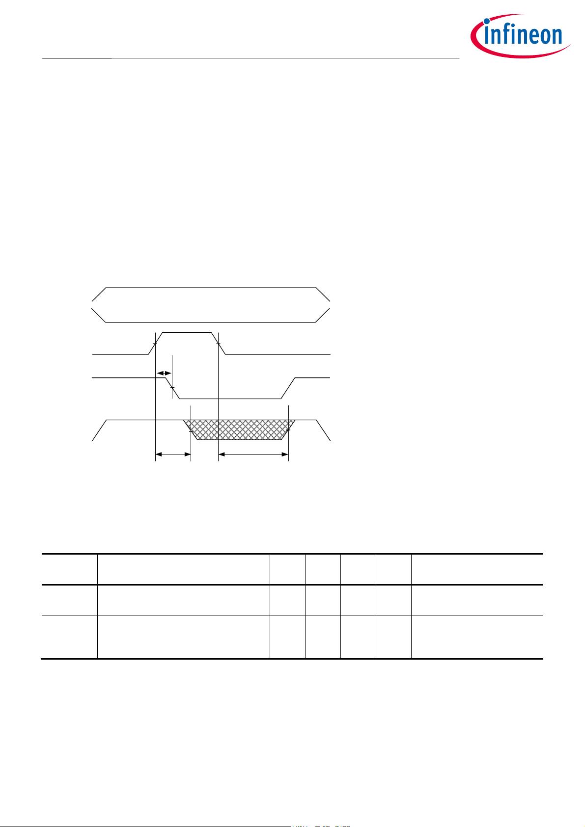
3.2 Maximum electrical rating
Table 3 Detailed description of absolute maximum ratings (IM393-M6E/F case)
Item Symbol Rating Description
Max. blocking
voltage
Output RMS
current
Output peak
current
Junction
temperature
Operating case
temperature
range
V
I
Peak
T
T
CES
I
600 V The sustained collector-emitter voltage of internal IGBTs
C
10 A
15 A
J
-40 ~ 150°C
The allowable RMS IGBT collector current at steady state and
Tc = 25 °C.
The allowable peak IGBT collector current at Tc = 25°C
Considering temperature ripple on the power chips, the
maximum junction temperature rating of IM393-XX is 150°C.
Tc (case temperature) is defined as a temperature of the
package surface underneath the specified power chip. Please
C
-40 ~ 125°C
mount a temperature sensor on a heat-sink surface at the
defined position in Figure 5 so as to get accurate temperature
information.
Figure 5 TC measurement point
3.3 Description of the input and output pins
The following tables define the DIP type of IM393-XX input and output pins. The detailed functional descriptions
are as follows:
Pin Name Description
1 P Positive bus input voltage
2 N/A None
3 VS(W) W-phase high side floating supply offset voltage
4 VB(W) W-phase high side floating supply voltage
5 N/A None
Application Note 10 of 53 V 1.0
2019-04-01
Page 11

IM393 Application note
IM393 IPM Technical Description
Product overview and pin description
6 VS(V) V-phase high side floating supply offset voltage
7 VB(V) V-phase high side floating supply voltage
8 N/A None
9 VS(U) U-phase high side floating supply offset voltage
10 VB(U) U-phase high side floating supply voltage
11 N/A None
12 VDD Low side control supply
13 VTH Temperature monitor
14 COM Low side control negative supply
15 COM Low side control negative supply
16 ITRIP Over current protection input
17 RFE RCIN / Fault / Enable
18 HIN(U) U-phase high side gate driver input
19 HIN(V) V-phase high side gate driver input
20 HIN(W) W-phase high side gate driver input
21 LIN(U) U-phase low side gate driver input
22 LIN(V) V-phase low side gate driver input
23 LIN(W) W-phase low side gate driver input
24 N(W) W-phase low side emitter
25 N(V) V-phase low side emitter
26 N(U) U-phase low side emitter
27 N(U) U-phase low side emitter (DIP only)
28 N(V) V-phase low side emitter (DIP only)
29 N(W) W-phase low side emitter (DIP only)
30 U U-phase output (DIP only)
31 V V-phase output (DIP only)
32 W W-phase output (DIP only)
33 P Positive bus input voltage (DIP only)
34 N/A None
35 P Positive bus input voltage (DIP only)
36 N/A None
Application Note 11 of 53 V 1.0
2019-04-01
Page 12

IM393 Application note
IM393 IPM Technical Description
Product overview and pin description
The following tables define the SIP type of IM393-XX input and output pins. The detailed functional descriptions
are as follows:
Pin Name Description
1 P Positive bus input voltage
2 N/A None
3 VS(W) / W W-phase high side floating supply offset voltage / W-phase output
4 VB(W) W-phase high side floating supply voltage
5 N/A None
6 VS(V) / V V-phase high side floating supply offset voltage / V-phase output
7 VB(V) V-phase high side floating supply voltage
8 N/A None
9 VS(U) / U U-phase high side floating supply offset voltage / U-phase output
10 VB(U) U-phase high side floating supply voltage
11 N/A None
12 VDD Low side control supply
13 VTH Temperature monitor
14 COM Low side control negative supply
15 COM Low side control negative supply
16 ITRIP Over current protection input
17 RFE RCIN / Fault / Enable
18 HIN(U) U-phase high side gate driver input
19 HIN(V) V-phase high side gate driver input
20 HIN(W) W-phase high side gate driver input
21 LIN(U) U-phase low side gate driver input
22 LIN(V) V-phase low side gate driver input
23 LIN(W) W-phase low side gate driver input
24 N(W) W-phase low side emitter
25 N(V) V-phase low side emitter
26 N(U) U-phase low side emitter
Application Note 12 of 53 V 1.0
2019-04-01
Page 13

IM393 Application note
IM393 IPM Technical Description
Product overview and pin description
High-side bias voltage pins for driving the IGBT
Pins: VB(U) – VS(U) , VB(V) – VS(V), VB(W) – VS(W)
• These pins provide the gate drive power to the high-side IGBTs.
• The ability to utilize a bootstrap circuit scheme for the high-side IGBTs eliminates the need for external power
supplies.
• Each bootstrap capacitor is charged from the V
IGBT or the freewheeling state of the low-side freewheeling diode.
• In order to prevent malfunctions caused by noise and ripple in the supply voltage, a good quality (low ESR,
low ESL) filter capacitor should be mounted very close to these pins.
Low-side bias voltage pin
Pin: VDD
• This is the control supply pin for the internal IC.
• In order to prevent malfunctions caused by noise and ripple in the supply voltage, a good quality (low ESR,
low ESL) filter capacitor should be mounted very close to this pin.
supply during the ON-state of the corresponding low-side
DD
Low-side common supply ground pin
Pin: COM
• This pin connects the control ground for the internal IC.
Signal Input pins
Pins: HIN(U), HIN(V), HIN(W), LIN(U), LIN(V), LIN(W)
• These are pins to control the operation of the internal IGBTs.
• They are activated by voltage input signals. The terminals are internally connected to a Schmitt trigger circuit
composed of 5 V-class CMOS.
• The signal logic of these pins is active-high. The IGBT associated with each of these pins will be turned ON
when a sufficient logic voltage is applied to these pins.
• The wiring of each input should be as short as possible to protect the IM393-XX against noise influences.
• To prevent signal oscillations, an RC coupling is recommended as illustrated in Figure 4.1.
Over-current detection pin
Pin: ITRIP
• The current-sensing shunt resistor should be connected between the pin N (emitter of low-side IGBT) and the
power ground to detect short-circuit current (refer to Figure 4.3). An RC filter should be connected between
the shunt resistor and the pin ITRIP to eliminate noise.
• The integrated comparator is triggered if the voltage V
selected to meet this level for the specific application. In case of a trigger event, the voltage at pin RFE is pulled
down to LOW.
• The connection length between the shunt resistor and ITRIP pin should be minimized.
Application Note 13 of 53 V 1.0
is higher than 0.49 V. The shunt resistor should be
ITRIP
2019-04-01
Page 14

IM393 Application note
IM393 IPM Technical Description
Product overview and pin description
RCIN/Fault/Enable input pin
Pin: RFE
• In case of an over-current event, the FLT/EN pin will get low with the turning ON of the open-drain MOSFET.
This pin is used to post I
• There are two situations in which the fault is reported via the RCIN/FLT/EN pin.
• The first is an undervoltage condition of V
pin will get low with the turning ON of the open-drain MOSFET.
• When the fault has been removed, the fault clear timer is started, and the length of the fault clear time period
is determined by the external capacitor value. (see section 5.2)
Temperature-monitoring output pin
Pin: VTH
• The VTH pin provides a voltage linked to NTC temperature. (see section 5.4)
to switch turn-OFF clear time. (see section 5.2)
TRIP
, the second is an over-current event condition, and the FLT/EN
DD
Positive DC-link pin
Pin: P
• This is the DC-link positive power supply pin of the IM393-XX IPM.
• It is internally connected to the collectors of the high-side IGBTs.
• In order to suppress the surge voltage caused by the DC-link wiring or PCB-pattern inductance, connect a
smoothing filter capacitor close to this pin. (Typically metal film capacitors are used.)
Negative DC-link pins
Pins: N(U), N(V), N(W)
• These are the DC-link negative power supply pins (power ground) of the inverter.
• These pins are connected to the low-side IGBT emitters of the each phase.
Inverter power output pins
Pins: U, V, W
• Inverter output pins for connecting to the inverter load (e. g. motor).
Application Note 14 of 53 V 1.0
2019-04-01
Page 15

IM393 Application note
IM393 IPM Technical Description
Product overview and pin description
3.4 Outline drawings
Figure 6 DIP version (IM393-X6E)
Figure 7 DIP version (IM393-X6E2)
Application Note 15 of 53 V 1.0
2019-04-01
Page 16

IM393 Application note
IM393 IPM Technical Description
Product overview and pin description
Figure 8 DIP version (IM393-X6E3)
Figure 9 SIP version (IM393-X6F)
Application Note 16 of 53 V 1.0
2019-04-01
Page 17

IM393 Application note
IM393 IPM Technical Description
Interface circuit and layout guide
4 Interface circuit and layout guide
4.1 Input/output signal connection
The following shows the I/O interface circuit between microcontroller and IM393-XX. Because the IPM input
logic is active-high with internal pull-down resistors, pulled-up resistors are not required. The RFE output is
open-drain MOSFET configured. Thus this signal should be pulled up to the positive side of 5 V or 3.3 V external
logic power supply with a resistor. The resistor should be carefully chosen to limit current (e.g. 1.2 MΩ). In case
of over-current, the RFE pin will get low as the MOSFET turns ON. When the over-current condition is over, the
MOSFET will then turn OFF, however, all the IGBTs will remain OFF until the fault is cleared (see section 5.3).
5V-Line (or 3.3V-Line)
CIPOSTM Tiny
HIN / LIN
RFE
COM
Micro
Controller
1nF
1kΩ
1.2MΩ
100Ω
1nF
1nF
Figure 10 Recommended microcontroller I/O interface circuit
Table 4 Maximum rating of input and RFE pin
Item Symbol Condition Rating Unit
Module supply voltage V
DD
Applied between
VDD – COM
Applied between
Input voltage V
IN
HIN(U), HIN(V), HIN(W) – COM
LIN(U), LIN(V), LIN(W) – COM
-0.3 ~ 20 V
-0.3 ~ 20 V
Fault output supply voltage RFE Applied between RFE – COM -0.3 ~ 20 V
The input and fault output maximum rating voltages are listed in Table 4. It is recommended to use 5 V logic
supply, which is the same for the input signals of the fault output. Bypass capacitors should be mounted as
close as possible to the RFE pin to avoid any noise that might switch the open-drain MOSFET ON.
Application Note 17 of 53 V 1.0
2019-04-01
Page 18

IM393 Application note
IM393 IPM Technical Description
Ω
≈
Ω
≈
Interface circuit and layout guide
CIPOSTM Tiny
HIN
k4
LIN
k4
Input
Noise
Filter
Deadtime &
Shoot
Through
Prevention
Input
Noise
Filter
Figure 11 Internal structure of signal input terminals
Because IM393-XX employs active-high input logic, the power sequence restriction between the control supply
and the input signal during start-up or shut-down operation does not exist. Therefore it makes the system failsafe. In addition, pull-down resistors are built into each input circuit. This reduces the required external
component count. Input Schmitt-trigger, noise filter, deadtime and shoot-through prevention functions
provide beneficial noise rejection to short input pulses. Furthermore, by lowering the turn ON and turn OFF
threshold voltage of the input signal as shown in Table 4.2, a direct connection to 3.3 V-class microcontroller or
DSP is possible.
Level shift
circuit
Delay
Gate driver
Gate driver
Table 5 Input threshold voltage (at VDD = 15 V and TJ = 25°C)
Item Symbol Condition Min. Typ. Max. Unit
Logic "1" input voltage V
Logic "0" input voltage V
IN,TH+
IN,TH-
LIN, HIN, RFE
2.5 - - V
- - 0.8 V
As shown in Figure 11, IM393-XX input signal integrates a 4 kΩ (typical) pull-down resistor. Therefore, when
using an external filtering resistor between the microcontroller output and IM393-XX input, attention should be
paid to the signal voltage drop at the IPM input terminal to satisfy the turn ON threshold voltage requirement.
For instance, R = 100 Ω and C = 1 nF for the parts shown in Figure 10.
Application Note 18 of 53 V 1.0
2019-04-01
Page 19
IM393 Application note
IM393 IPM Technical Description
Interface circuit and layout guide
4.2 Input/output signal connection
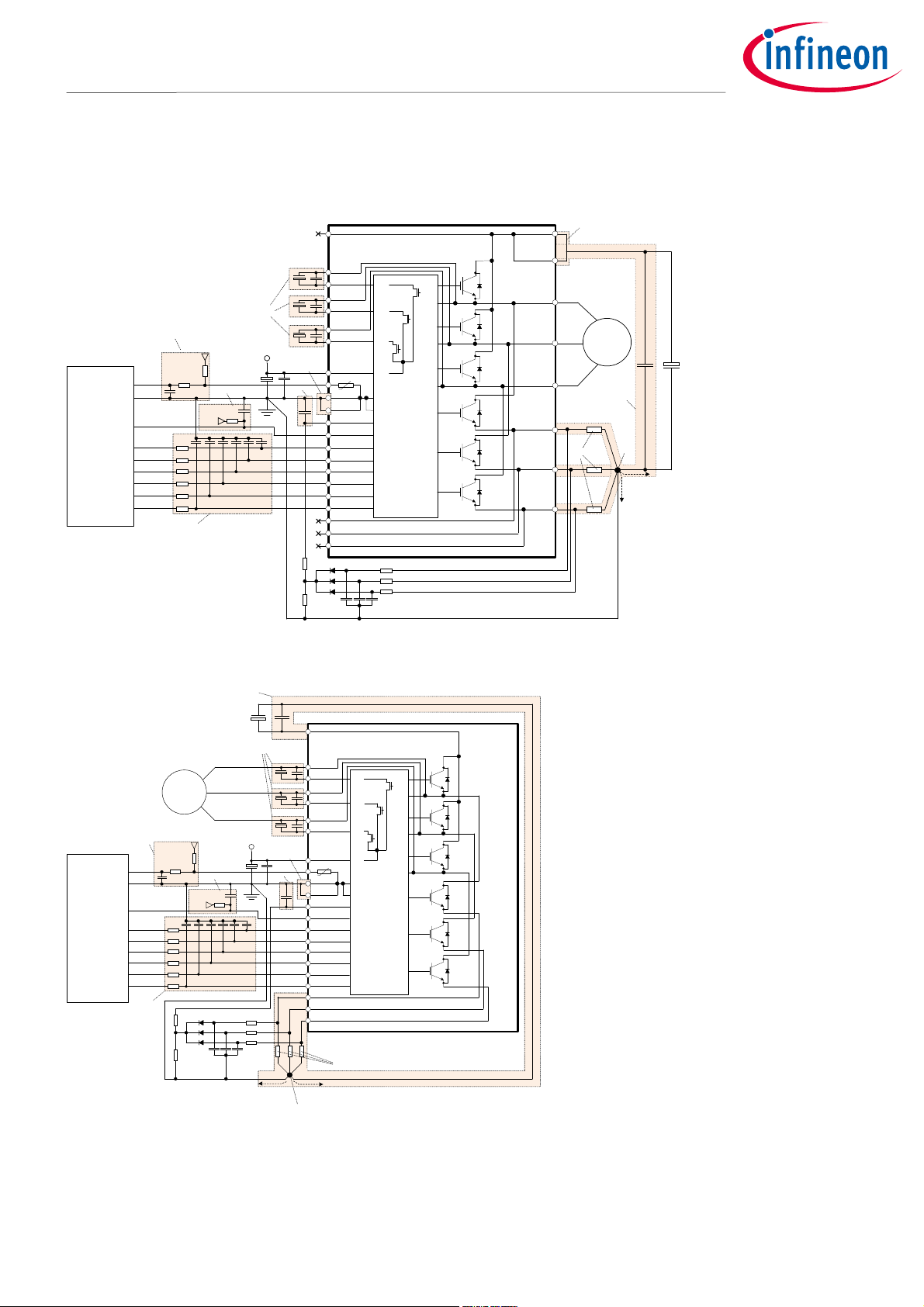
Figure 4.3 and 4.4 show a typical application circuit interface schematic with control signals connected directly
to the microcontroller.
P (35)
P (33)
W (32)
V (31)
U (30)
#10
3-ph AC
Motor
#5
#6
#7
Power GND
Control GND
Micro
Controller
(1) P
(3) VS(W)
(4) VB(W)
VB3
(6) VS(V)
(7) VB(V)
#4
#3
5 or 3.3V
15V
#8
#9
#2
5 or 3.3V
#1
(9) VS(U)
(10) VB(U)
(12) VDD
(13) VTH
-t°
(14) COM
(15) COM
(16) ITRIP
(17) RFE
(18) HIN(U)
(19) HIN(V)
(20) HIN(W)
(21) LIN(U)
(22) LIN(V)
(23) LIN(W)
(24) N(W)
(25) N(V)
(26) N(U)
VB2
VB1
VDD
COM
VSS
ITRIP
RFE
HIN1
HIN2
HIN3
LIN1
LIN2
LIN3
HO3
VS3
HO2
VS2
HO1
VS1
LO3
LO2
LO1
N(W) (29)
N(V) (28)
N(U) (27)
Figure 12 Example of application circuit (DIP package)
#5
(1) P
#4
(3) VS(W)
(4) VB(W)
VB3
VB2
VB1
VDD
COM
VSS
ITRIP
RFE
HIN1
HIN2
HIN3
LIN1
LIN2
LIN3
HO3
VS3
HO2
VS2
HO1
VS1
LO3
LO2
LO1
Micro
Controller
3-ph AC
Motor
5 or 3.3V
#3
15V
#9
5 or 3.3V
#1
(6) VS(V)
(7) VB(V)
(9) VS(U)
(10) VB(U)
#8
(12) VDD
(13) VTH
#2
-t°
(14) COM
(15) COM
(16) ITRIP
(17) RFE
(18) HIN(U)
(19) HIN(V)
(20) HIN(W)
(21) LIN(U)
(22) LIN(V)
(23) LIN(W)
(24) N(W)
(25) N(V)
(26) N(U)
#6
Control GND
Power GND
#7
Figure 13 Example of application circuit (SIP package)
Application Note 19 of 53 V 1.0
2019-04-01
Page 20

IM393 Application note
IM393 IPM Technical Description
Interface circuit and layout guide
Notes:
1. Input circuit
- RC filter can be used to reduce input signal noise. (100 Ω, 1 nF)
- The capacitors should be located close to CIPOS™ Tiny (to COM terminal especially).
2. Itrip circuit
- To prevent a malfunctioning of the protection function, an RC filter is recommended.
- The capacitor must be located close to Itrip and COM terminals.
3. VTH circuit
- This terminal should be pulled up to the bias voltage of 5 V/3.3 V by a proper resistor to define suitable
voltage for temperature monitoring.
- It is recommended that the RC filter be placed close to the controller.
4. VB-VS circuit
- Capacitors for high-side floating supply voltage should be placed close to VB and VS terminals.
- Additional high-frequency capacitors, typically 0.1 μF, are strongly recommended.
- Overlap of pattern-to-motor and pattern-to-bootstrap capacitors should be minimized. (SIP only)
5. Snubber capacitor
- The wiring between CIPOS™ Tiny, snubber capacitor and shunt resistors should be as short as possible.
6. Shunt resistor
- SMD-type shunt resistors are strongly recommended to minimize internal stray inductance.
7. Ground pattern
- Pattern overlap of power ground and signal ground should be minimized. The patterns should be
connected at the common end of the shunt resistors only, for the same potential.
8. COM pattern
- In the case of a DIP package, pins 24, 25 and 26 must be left unconnected, as COM is connected to pin 29, 28
and 27 by the shunt resistor.
- It is highly advisable to connect both pins 14 and 15 together.
9. RFE circuit
- To set up R and C parameters for fault-clear time, please refer to Figure 5.
- For normal operation, RFE (pin 17) should always be pulled up to 5 V or 3.3 V via the pull resistor.
- This R is also mandatory for fault reporting function, as it is an open-drain structure.
10. P pattern
- In the case of a DIP package, pin 1 can be left unconnected, as positive bus voltage is connected by pins 35
and 33 that are internally connected to pin 1.
4.3 Recommended circuit current of power supply
Control and gate driver power for the IM393-XX is normally provided by a single 15 V supply that is connected to
the module VDD Pin. The circuit current of VDD control supply of IM393-L6E is shown in below Table 6.
Table 6 The circuit current of control power supply of IM393-L6E (Unit:[mA])
Item Static (Typ.) Dynamic (Typ.) Total (Typ.)
V
= 15 V
DD
V
= 20 V FSW = 20 kHz 8.03 4.08 12.11
DD
And the circuit current of the 5 V logic power supply (VTH, RFE and input terminal) is about 20 mA.
Finally, the recommended minimum circuit currents of power supply considering margins are shown in Table 7.
Application Note 20 of 53 V 1.0
FSW = 5 kHz 4.02 0.26 4.28
FSW = 15 kHz 4.02 0.78 4.83
2019-04-01
Page 21
IM393 Application note
IM393 IPM Technical Description
Interface circuit and layout guide
Table 7 The recommended minimum circuit current of control power supply (Unit:[mA])
Item The circuit current of +15 V control supply The circuit current of +5 V logic supply
VDD ≤ 20 V,
FSW ≤ 20 kHz
90 45
4.4 Recommended layout for over-current protection (OCP) and shortcircuit protection (SCP) functions
It is recommended to make the I
ITRIP filter capacitor should be connected to the COM pin directly without overlapping ground pattern. The
signal ground and power ground should be as short as possible and connected at only one point via the filter
capacitor of VDD line. The I
function combined with the external shunt resistor can be used to detect over-
TRIP
current events in the ground path that will result in damages to the IPM. The internal HVIC gate driver
continuously monitors the voltage on ITRIP pin. If this voltage exceeds the reference voltage (typ. 0.49 V), a
fault signal will be generated on the RFE pin and all six IGBTs will be turned OFF.
VDD line
Micro
Controller
5 or 3.3V line
filter capacitor connections to the IM393-XX pins as short as possible. The
TRIP
CIPOSTM Tiny
(12) VDD
(14,15) COM
(16) ITRIP
(1) P
(17) RFE
(18~23) HIN/LIN
(24~26) Nx
Figure 14 Example of layout pattern for OCP and SCP functions
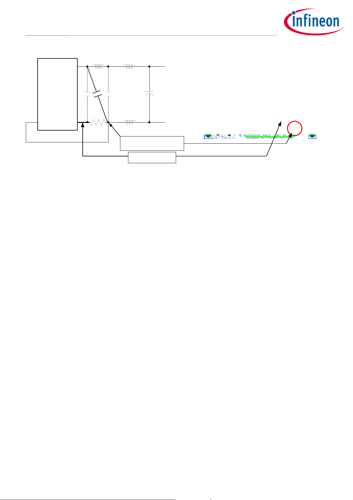
4.5 Recommended wiring of shunt resistor and snubber capacitor
External current-sensing resistors are applied to detect over-current of phase currents. A long wiring pattern
between the shunt resistors and IM393-XX will cause excessive surges that might damage the IPM-internal IC
and current-detection components. This may also distort the sensing signals that may lead to loss of control
when driving a motor. To decrease the pattern inductance, the wiring between the shunt resistors and the
IM393-XX should be as short as possible, and any loop should be avoided.
As shown in Figure 15, snubber capacitors should be installed in the right location so as to suppress surge
voltages effectively. Generally a high-frequency, non-inductive capacitor of around 0.1 ~ 0.22 µF is
recommended. If the snubber capacitor is installed in the wrong location, ‘1’ as shown in Figure 15, the snubber
capacitor cannot suppress the surge voltage effectively. If the capacitor is installed in location ‘2’, the charging
and discharging currents generated by wiring inductance and the snubber capacitor will appear on the shunt
resistor. This will impact the current-sensing signal, and the SC protection level will be a little lower than the
calculated design value. The “2” position surge suppression effect is greater than in locations ‘1’ or ‘3’. The ‘3’
position is a reasonable compromise with better suppression than in location ‘1’ without impacting the
current-sensing signal accuracy. For this reason, location ‘3’ is generally used.
Application Note 21 of 53 V 1.0
2019-04-01
Page 22
IM393 Application note
IM393 IPM Technical Description
Interface circuit and layout guide
CIPOS
TM
P
3
12
Wiring Leakage
NVSS
Shunt
Resistor
Inductance
Please make the one point connection
point as close as possible to the GND
terminal of shunt resistor
Wiring inductance should
be less than 10nH
Capacitor
Bank
PCB layout example - CIPOSTM Reference Board
Figure 15 Recommended wiring of shunt resistor and snubber capacitor
General suggestions and summary:
• PCB traces should be designed as short as possible and the area of the circuit (power or signal) should be
minimized to avoid any noise.
• Make sure there is a good distance between switching lines with high di/dt and dV/dt and the signal lines, as
they are very sensitive to electrical noise. Specifically, the trace of each phase OUT carrying significant fast
current and voltage transition should be separated from the logic lines and analog sensing circuit (R
SHUNT
, I
TRIP
RFE).
• Place shunt resistors as close as possible to the low-side pins of the IPM. Parasitic inductance should be as
low as possible. Use of a low-inductance SMD resistor is highly advisable.
• Avoid any ground loop. Only a single path must connect to COM.
• Place each RC filter as close as possible to the IPM pins to increase its efficiency.
• Fixed voltage traces such as GND and high voltage lines can be used to shield the logic and analog lines from
electrical noise produced by the switching lines.
,
Application Note 22 of 53 V 1.0
2019-04-01
Page 23

IM393 Application note
IM393 IPM Technical Description
Interface circuit and layout guide
4.6 Pin and screw hole coordinates for IM393-XX footprint
Figure 16 shows IM393-XX position on the PCB to indicate center coordinates of each pin and screw hole in
Table 8 and Table 9.
(a) Dual in-line package
(b) Single in-line package
Figure 16 IM393-XX positions on PCB
Application Note 23 of 53 V 1.0
2019-04-01
Page 24
IM393 Application note
IM393 IPM Technical Description
Interface circuit and layout guide
Table 8 Pin and screw hole coordinates for DIP package (Unit:[mm])
Pin Number X Y Pin Number X Y
Signal pin
1 0.00 0.00
20 24.13 3.00
2 N/A N/A 21 25.40 0.00
3 2.54 3.00 22 26.67 3.00
4 3.81 0.00 23 27.94 0.00
Signal pin
5 N/A N/A 24 29.21 3.00
6 6.35 3.00 25 30.48 0.00
7 7.62 0.00 26 31.75 3.00
8 N/A N/A
27 30.48 -19.00
9 10.16 3.00 28 27.94 -19.00
10 11.43 0.00 29 25.40 -19.00
11 N/A N/A 30 21.59 -19.00
12 13.97 3.00 31 17.78 -19.00
Power pin
13 15.24 0.00 32 13.97 -19.00
14 16.51 3.00 33 10.16 -19.00
15 17.78 0.00 34 N/A N/A
16 19.05 3.00 35 2.54 -19.00
17 20.32 0.00 36 N/A N/A
18 21.59 3.00
19 22.86 0.00 2 -0.13 -9.50
Screw
hole
1 31.87 -9.50
Table 9 Pin and screw hole coordinates for SIP package (Unit:[mm])
Pin Number
1 0.00 0.00
X Y
Pin Number
14 16.51 -3.00
2 N/A N/A 15 17.78 0.00
3 2.54 -3.00 16 19.05 -3.00
4 3.81 0.00 17 20.32 0.00
5 N/A N/A 18 21.59 -3.00
6 6.35 -3.00 19 22.86 0.00
Signal pin
7 7.62 0.00 20 24.13 -3.00
Signal pin
8 N/A N/A 21 25.40 0.00
9 10.16 -3.00 22 26.67 -3.00
10 11.43 0.00 23 27.94 0.00
11 N/A N/A 24 29.21 -3.00
12 13.97 -3.00 25 30.48 0.00
13 15.24 0.00 26 31.75 -3.00
X Y
Application Note 24 of 53 V 1.0
2019-04-01
Page 25
IM393 Application note
IM393 IPM Technical Description
Function and protection circuit
5 Function and protection circuit
5.1 Over-current protection
IM393-XX is equipped with an I
input pin. Together with an external shunt resistor, this functionality can be
TRIP
used to detect over-current events in the negative DC bus. The internal HVIC gate driver will continuously
monitor the voltage on the I
pin. Whenever this voltage exceeds the reference voltage (typ. 0.49 V), a fault
TRIP
signal will be generated on the RFE pin, and all six IGBTs will be turned OFF. Typically, the maximum shortcircuit current magnitude is gate-dependent. A higher gate voltage results in a larger short-circuit current. In
order to avoid this potential problem, the maximum over-current trip level is generally set below twice the
nominal rated collector current.
5.1.1 Timing chart of over-current protection (OCP)
HIN(U, V, W)
LIN(U, V, W)
I
TRIP
RFE
U, V, W
50%
T
FLT
50%
50%
50%
50%
T
ITRIP
T
FLT-CLR
Figure 17 Timing chart of over-current protection function
The threshold of over-current protection can be determined by V
directly connected to I
pin. The following table shows the delay time of fault reporting and I
TRIP
ITRIP+
/ R
, if a single bus shunt is used, and is
SHUNT
shutdown:
TRIP
Table 10 Dynamic electrical characteristics
Symbol Description Min. Typ. Max. Unit conditions
T
T
FLT
ITRIP
I
to fault propagation delay 400 600 800 ns V
TRIP
I
to six switches turn OFF
TRIP
propagation delay
- - 1.5 μs IC = 5 A, V
= 0 V or 5 V, V
IN
= 300 V
DC
ITRIP
= 5 V
In the case of a short-circuit, the current level will rise very quickly to the saturation current of the IGBT. It is
critical to ensure that all IGBTs are turned OFF as soon as possible. Since the IGBTs in IM393-XX are short-circuit
rated (see Table 11), the safe operating of the IPM is guaranteed by minimizing the delay of the external currentsensing circuit, and ensuring its delay plus T
is less than the IGBT short-circuit rating time. Because IGBT short
ITRIP
circuit rating depends a lot on the gate voltage that is influenced by VDD and junction temperature, it is important
to consider all possible conditions.
Application Note 25 of 53 V 1.0
2019-04-01
Page 26

IM393 Application note
IM393 IPM Technical Description
0.8
Function and protection circuit
Table 11 IGBT short-circuit ratings
Item Symbol Condition Value Unit
Short-circuit withstand time T
SC
TJ < 150 °C, VDC = 360 V, VDD = 15 V 3 μs
5.1.2 Selecting current-sensing shunt resistor
The value of the current-sensing resistor is calculated by the following equation:
V
THIT,
R
=
SH
Where
V
OC detection level.
The maximum value of the OC protection level should be set lower than the repetitive peak collector current in
the datasheet considering the tolerance of the shunt resistor.
For example, the maximum peak collector current of IM393-L6E/F is 22.5 A
value of the shunt resistor is calculated as
()
For the power rating of the shunt resistor, the following list should be considered:
• Maximum load current of inverter (I
• Shunt resistor value at Tc = 25°C (R
• Power derating ratio of shunt resistor at T
• Safety margin
+
I
OC
is the ITRIP positive-going threshold voltage of IM393-XX. It is typically 0.49 V. IOC is the current of
+THIT,
, and thus, the recommended
peak
0.49
=
22.5
= 0.022 Ω
SH
RMS
)
)
= 100°C according to the manufacturer’s datasheet
SH
(1)
The shunt resistor power rating is calculated by the following equation:
2
SH
rms
=
P
SH
marginRI
××
ratioderating
For example with IM393-L6E/F and RSH = 22 mΩ:
• Max. load current of the inverter : 6 A
• Power derating ratio of shunt resistor at T
• Safety margin : 30 %
2
P
=
SH
1.30.0225
××
W0.9
=
RMS
=100°C : 80 %
SH
A proper power rating of shunt resistor should then exceed 1 W, e.g. 1.5 W.
Based on the previous equations, conditions, and calculation method, the minimum shunt resistance and
resistor power according to IM393-XX products have been introduced and are listed in Table 12.
Note that a proper resistance and power rating, which is higher than the minimum value, should be chosen
considering the over-current protection level required in the application.
(2)
Application Note 26 of 53 V 1.0
2019-04-01
Page 27

IM393 Application note
IM393 IPM Technical Description
Function and protection circuit
Table 12 Minimum RSH and P
Product Maximum peak current
IM393-X6E/F 30 A
IM393-L6E/F 22.5 A
IM393-M6E/F 15 A
IM393-S6E/F 9 A
SH
Minimum shunt resistance,
R
SH
16 mΩ
22 mΩ
33 mΩ
54 mΩ
Minimum shunt resistor
power, P
SH
3 W
2 W
1.5 W
1 W
5.1.3 Delay time
The RC filter is necessary in the over-current sensing circuit to prevent malfunction of OC protection caused by
noise. The RC time constant is determined by applying time of noise and the withstand time capability of IGBT.
When the sensing voltage on the shunt resistor exceeds I
applied to the ITRIP pin of the IM393-XX via the RC filter. Table 13 shows the specification of the OC protection
reference level. The filter delay time (T
rises to the I
positive threshold voltage during T
TRIP
) is caused by RC filter time constant, and the input voltage of I
FILTER
FILTER
In addition there is the shutdown propagation delay of I
Table 13 Specification of OC protection reference level ‘V
positive-going threshold (V
TRIP
.
. Please refer to Table 14.
TRIP
’
IT,TH+
), this voltage is
IT,TH+
TRIP
pin
Item Min. Typ. Max. Unit
I
positive going threshold V
TRIP
IT,TH+
0.44 0.49 0.54 V
Table 14 Internal delay time of OC protection circuit
Item Condition Min. Typ. Max. Unit
Shut down
propagation
delay (T
ITRIP
)
IM393-X6E/F I
IM393-L6E/F I
IM393-M6E/F I
IM393-S6E/F I
= 10 A, from V
out
= 7.5 A, from V
out
= 5 A, from V
out
= 3 A, from V
out
IT,TH+
IT,TH+
IT,TH+
IT,TH+
to 10 % I
to 10 % I
to 10 % I
to 10 % I
out
out
out
out
- - 1.5 μs
- - 1.5 μs
- - 1.5 μs
- - 1.5 μs
Therefore the total time from over-current event to shut down of all six IGBTs is:
T
= T
TOTAL
Shut-down propagation delay is inversely proportional to the current range; therefore the T
FILTER
+ T
ITRIP
is reduced at
ITRIP
(3)
higher current conditions than those in Table 14. The recommended total delay is less than the 3 μs of safety
operation. Thus, the RC time constant should be set in the range of 1~1.5 µs. Recommended values for the filter
components are R = 1.5 kΩ and C = 1 nF.
5.2 Fault output and auto-clear function
As described in the previous section, in the event of an over-current, the RFE pin will get low as the I
high when the open-drain MOSFET is turned on. When over-current conditions end, the open-drain MOSFET will
be turned off, as illustrated in Figure 18. However, all IGBTs will remain off until RFE voltage can reach a positivegoing threshold. This is called the fault auto-clear function, and is shown as T
Application Note 27 of 53 V 1.0
in Figure 19.
FLT-CLR
pin gets
TRIP
2019-04-01
Page 28

IM393 Application note
IM393 IPM Technical Description
Function and protection circuit
HIN(X)
HIN(X)
LIN(X)
LIN(X)
COM
COM
Input
Noise
filter
Input
Noise
filter
Deadtime &
Shoot-Through
Prevention
VDD
Under-
voltage
detection
To Microcontroller
ITRIP
ITRIP
+3.3V
R
RCIN
C
RCIN
RFE
Noise
filter
ITRIP
Noise
filter
Figure 18 Internal block diagram of IM393-XX
HIN(U, V, W)
LIN(U, V, W)
I
TRIP
50%
T
FLT
50%
RFE
U, V, W
T
Figure 19 Input-output timing chart during short-circuit event
The T
can be determined by the below formula.
FLT-CLR
In the case of 3.3 V,
V
(t) = 3.3 V * (1 – e
RFE
T
= - R
FLT-CLR
RCIN
For example, if R
Application Note 28 of 53 V 1.0
-t/RC
) (4)
* C
* ln (1-V
RCIN
is 1.2 MΩ and C
RCIN
50%
ITRIP
50%
50%
T
FLT-CLR
/3.3 V) (5)
IN_TH+
is 1 nF, the T
RCIN
is about 1.7 ms with V
FLT-CLR
IN_TH+
of 2.5 V.
2019-04-01
Page 29

IM393 Application note
IM393 IPM Technical Description
Function and protection circuit
It is also important to note that C
needs to be minimized in order to make sure it is fully discharged in the
RCIN
event of over-current. Since the ITRIP pin has a 350 ns input filter, it is appropriate to ensure that C
discharged below V
V
(t) = 3.3 V * e
RFE
C
< 350 ns / (- ln (V
RCIN
Considering V
-t/RC
IN_TH-
by the open-drain MOSFET, after 350 ns. Therefore, the max C
IN_TH-
< V
IN_TH-
/ 3.3 V) * R
IN_TH-
of 0.8 V and R
RFE_ON
) (7)
RFE_ON
of 50 Ω, C
should be less than 4.9 nF.
RCIN
can be calculated as:
RCIN
In the case of 5 V,
V
(t) = 5 V * (1 – e
RFE
T
= - R
FLT-CLR
RCIN
For example, if R
The max C
V
RFE
C
RCIN
RCIN
(t) = 5 V * e
< 350 ns / (- ln (V
-t/RC
) (8)
* C
* ln (1-V
RCIN
is 1.2 MΩ and C
RCIN
IN_TH+
can be calculated as:
-t/RC
< V
IN_TH-
/ 5 V) * R
IN_TH-
/5 V) (9)
is 1 nF, the T
RCIN
) (11)
RFE_ON
is about 0.8 ms with V
FLT-CLR
IN_TH+
of 2.5 V.
will be
RCIN
(6)
(10)
Considering V
As far as R
RCIN
interfere with the discharging of C
of 0.8 V and R
IN_TH-
RFE_ON
of 50 Ω, C
should be less than 3.8 nF.
RCIN
is concerned, it should be selected to achieve the desired T
in the case of over-current. Also it cannot be too high in order to ensure
RCIN
. Its value should not be too low to
FLT-CLR
proper biasing of the RFE pin during normal operation. A resistor value between 0.5 MΩ and 2 MΩ is suggested to
have a fault-clear time in the range of 1 ms.
It is critical that the PWM generator be disabled within the fault duration to guarantee a shutdown of the system,
and the over-current condition must be cleared before resuming operation.
5.3 Undervoltage lockout (UVLO)
IM393-XX HVIC provides undervoltage lockout protection on both the V
supply and the V
(high-side circuitry) power supply. Figure 20 is used to illustrate this concept. V
BS
plotted over time, and as the waveform crosses the UVLO threshold (V
protection is enabled or disabled.
Upon power-up, should the V
VDD voltage decreases below the V
voltage fail to reach V
DD
threshold during operation, the undervoltage lockout circuitry will
DDUV-
threshold, the IC will not turn on. Additionally, if the
DDUV+
recognize a fault condition, and shut down the high and low-side gate drive outputs. The RFE pin will then go to
the low state to inform the controller of the fault condition.
Upon power-up, should the V
the V
voltage decreases below the V
BS
voltage fail to reach the V
BS
threshold during operation, the undervoltage lockout circuitry will
BSUV-
threshold, the IC will not turn on. Additionally, if
BSUV+
recognize a fault condition, and shut down the high-side gate drive outputs of the IC.
(logic and low-side circuitry) power
DD
or VBS is
DD
DDUV+/-
or V
), the undervoltage
BSUV+/-
The UVLO protection ensures that the IC drives the power devices only when the gate supply voltage is
sufficient to fully enhance the power devices. Without this feature, the power switch could be driven with a low
gate voltage which results in excessive losses, as it conducts current while the channel impedance is high.
When conduction losses are too high within the power switch, it could lead to power switch failure.
Application Note 29 of 53 V 1.0
2019-04-01
Page 30

IM393 Application note
IM393 IPM Technical Description
V
Fault Output Signal
V
Fault Output Signal
Function and protection circuit
V
DDUV-
(or V
)
BSUV-
UVLO Protection
(Gate Dr ive Outpu ts Dis abled)
Normal
Operation
Figure 20 UVLO protection
DDUV+
Control
Supply Voltage
V
DDUV+
(or V
)
BSUV+
Time
Normal
Operation
V
DDUV-
HINx
LINx
HOx
LOx
Figure 21 Timing chart of low-side undervoltage protection function
BSUV+
Control
Supply Voltage
V
BSUV-
HINx
LINx
HOx
LOx
High-level (no fault output)
Figure 22 Timing chart of high-side undervoltage protection function
Table 15 IM393-XX functions versus control power supply voltage
Control voltage range [V] IM393-XX function operations
0 ~ 4
Application Note 30 of 53 V 1.0
Control IC is not operating. Undervoltage lockout function is not working and
fault output signal is not provided.
2019-04-01
Page 31

IM393 Application note
IM393 IPM Technical Description
Function and protection circuit
4 ~ 11.2
As the undervoltage lockout function is activated, control input signals are
blocked, and a fault signal VFO is generated.
IGBTs will be operated in accordance with the control gate input. Driving
11.2 ~ 13.5
voltage is below the recommended range, so V
will be larger than under normal conditions. High-side IGBTs cannot operate
after VBS initial charging, as VBS cannot reach V
13.5 ~ 16.5 for VDD
12.5 ~ 17.5 for VBS
Normal operation. This is the recommended operating condition.
VDD of 15 V is recommended when only integrated bootstrap circuitry is used.
IGBTs are still in operation. Because driving voltage is above the
16.5 ~ 20 for VDD
17.5 ~ 20 for VBS
recommended range, IGBTs’ switching is faster. It causes increased system
noise. And peak short-circuit current might be too large for proper operation
of the short-circuit protection.
Over 20 Control circuit in the IM393-XX might be damaged.
5.4 Over-temperature protection
and the switching losses
CE(sat)
.
BSUV+
IM393-XX have VTH pins for temperature-sensing. Figure 23 shows internal thermistor-resistance characteristics
according to the thermistor temperature. For over-temperature protection, a circuitry is introduced in this
section. As shown in Figure 24, the VTH pin is connected directly to the ADC terminal of the microcontroller. This
circuit is very simple, and the six IGBTs have to be shut down by a command issued from the microcontroller.
Figure 23 Internal thermistor-resistance characteristics according to thermistor temperature
NTC resistance can be translated to a voltage that can be read by the microcontroller using external resistance
R1. For example, when R1 is 2 kΩ, then VFO at about 100°C of the thermistor temperature is 2.95 V
and 1.95 V at V
Application Note 31 of 53 V 1.0
= 3.3 V, as shown in Figure 25.
ctr
typ
at V
= 5 V
ctr
2019-04-01
Page 32
IM393 Application note
IM393 IPM Technical Description
℃ : 2.95 V at Vctr = 5 V
℃ : 1.95 V at Vctr = 3.3 V
Function and protection circuit
Vctr
R1
CIPOSTM Tiny
ADC
VTH
Thermistor
COM
Figure 24 Circuit proposals for over-temperature protection
5.0
Vctr = 5 V
Vctr = 3.3 V
[V]
V
TH
4.5
4.0
3.5
3.0
2.5
2.0
1.5
1.0
OT set 100
OT set 100
0.5
0.0
0 10 20 30 40 50 60 70 80 90 100 110 120
Thermistor temperature [℃]
Figure 25 Voltage of VTH pin according to thermistor temperature
Application Note 32 of 53 V 1.0
2019-04-01
Page 33
IM393 Application note
IM393 IPM Technical Description
Bootstrap circuit
6 Bootstrap circuit
6.1 Bootstrap circuit operation
The VBS voltage, which is the voltage difference between V
B (U, V, W)
and V
, provides the supply to the IC
S (U, V, W)
within the IM393-XX. This supply voltage must be in the range of 12.5~17.5 V to ensure that the IC can fully drive
the high side IGBT. IM393-XX includes an under-voltage detection function for the VBS to ensure that the IC does
not drive the high-side IGBT if the VBS voltage drops below a specified voltage (section 5.3).
Internal bootstrap circuitry is integrated inside the HVIC. It consists of three high-voltage MOSFETs that
eliminate the need for an external circuitry (diodes + resistors). There is one MOSFET for each high-side output
channel, which is connected between the VDD supply and its respective floating supply (V
B(U)
, V
B(V)
, V
B(W)
), as
shown in Figure 26. The integrated bootstrap MOSFET is turned ON only when the low-side output (LO) is
“HIGH”, and has a limited source-current due to RBS. The VBS voltage will be charged each cycle depending on
the time of LO and the value of the CBS capacitor, the collector-emitter drop of external IGBT and the low-side
freewheeling diode drop.
The bootstrap MOSFET of each channel follows the state of respective low-side output stage unless the V
voltage is higher than approximately 110% of V
In that case, the bootstrap MOSFET is designed to remain OFF
DD.
B
until VB returns below that threshold. This concept is illustrated in Figure 27.
V
B(U)
V
DD
V
B(V)
V
B(W)
Figure 26 Internal bootstrap MOSFET connections
Bootstrap
MOSFET
disabled
Time
OFF
Vth ~1.1(VDD)
VDD=15V
Bootstrap
MOSFET
state
V
LO
BS
ON ON
Figure 27 Bootstrap MOSFET state diagram
A bootstrap MOSFET is suitable for most of the PWM modulation schemes, and can be used either in parallel
with an external bootstrap network or as a replacement of it. The use of the integrated bootstrap as a
replacement of the external bootstrap network may have some limitations however. An example of this
limitation may arise when this functionality is used in non-complementary PWM schemes and at very high PWM
duty cycle. In these cases, superior performance can be achieved by using an external bootstrap diode and
resistor in parallel with the internal bootstrap network.
Application Note 33 of 53 V 1.0
2019-04-01
Page 34
IM393 Application note
IM393 IPM Technical Description
ΔV
×
Bootstrap circuit
Table 16 Electrical characteristics of internal bootstrap parameters
Item Symbol
Unit
Min. Typ. Max.
Value
Bootstrap resistance R
BS
- 200 -
Ω
6.2 Initial charge of bootstrap capacitor
Adequate on-time duration of the low-side IGBT to fully charge the bootstrap capacitor is required for initial
bootstrap charging. The bootstrap capacitor needs to be pre-charged in order to limit peak current and power
through the resistor. The initial charging time (t
1
RCt
BSBScharge
• V
= Forward voltage drop across the bootstrap diode
FD
• V
• V
= The minimum value of the bootstrap capacitor voltage
BS(min)
= Voltage drop across the low-side IGBT
LS
ln(
×××≥
δ
• δ = Duty ratio of PWM
CIPOSTM Tiny
C
BS
VS
VB
VB
HO
VS
V
DD
U, V, W
P
U
) can be calculated with the following equation:
charge
)
VVVV
−−−
LSFDBS(min)DD
(12)
LIN
VDD
COM
LIN
VDD
LO
VSS
N
LIN
15V line
(a) Bootstrap circuit (b) Timing chart of initial bootstrap charging
Figure 28 Bootstrap circuit operation and initial charging
6.3 Bootstrap capacitor selection
The bootstrap capacitance can be calculated by:
ΔtI
C
BS
• Whereby,
• Δt = maximum ON pulse width of high-side IGBT
• ΔV = the allowable discharge voltage of the C
leak
=
.
BS
(13)
Application Note 34 of 53 V 1.0
2019-04-01
Page 35

IM393 Application note
IM393 IPM Technical Description
≥4.
7×
200Ω×
1
0.5
×
ln
15
15−12.
5−0.
1
≅3.
4
Bootstrap circuit
• I
= maximum discharge current of the CBS mainly via the following mechanisms:
leak
− Gate charge for turning on the high-side IGBT
− Quiescent current to the high-side circuit in the IC
− Level-shift charge required by level shifters in the IC
− Leakage current in the bootstrap diode
− C
capacitor leakage current (ignored for non-electrolytic capacitors)
BS
− Bootstrap diode reverse-recovery charge
In practice, a leakage current of 1mA is recommended as a calculation basis for IM393-XX. By taking into
consideration dispersion and reliability, the capacitance is generally selected to be 2 to 3 times higher than the
calculated one. The CBS is only charged when the high-side IGBT is off, and the VS voltage is pulled down to
ground. Therefore, the on-time of the low-side IGBT must be sufficient to ensure that the charge drawn from
the CBS capacitor can be fully replenished. Hence, there is inherently a minimum on-time of the low-side IGBT
(or off-time of the high-side IGBT).
The bootstrap capacitor should always be placed as close to the IM393-XX pins as possible. At least one low ESR
capacitor should be used to provide good local de-coupling. For example, a separate ceramic capacitor close to
IM393-XX is essential, if an electrolytic capacitor is used for the bootstrap capacitor. If the bootstrap capacitor is
either a ceramic or tantalum type, it should be adequate for local decoupling.
6.4 Charging and discharging of the bootstrap capacitor during PWM
inverter operation
The bootstrap capacitor CBS charges through the bootstrap MOSFET from the VDD supply when the high-side
IGBT is off, and the VS voltage is pulled down to ground. It discharges when the high-side IGBT or diode are on.
Example: Selection of the initial charging time
An example of the calculation of the minimum value of the initial charging time
Conditions:
• C
= 4.7 µF, RBS = 200 Ω, Duty Ratio (δ)= 0.5, VDD = 15 V,
BS
• V
•
In order to ensure safety, it is recommended that the charging time be at least three times longer than the
calculated value.
Example 2: The minimum value of the bootstrap capacitor
Conditions:
= 12.5 V, VLS = 0.1 V
BS (min)
ΔV=0.1 V, I
Application Note 35 of 53 V 1.0
=1 mA
leak
2019-04-01
Page 36

IM393 Application note
IM393 IPM Technical Description
Bootstrap circuit
5
4
3
[uF]
BS
2
C
1
0
0 5 10 15 20
f
[kHz]
PWM
Figure 29 Bootstrap capacitance as a function of the switching frequency
Figure 29 shows the curve for a continuous sinusoidal modulation. If the voltage ripple is 0.1 V, the
recommended bootstrap capacitance is therefore in the range of 4.7 µF for most switching frequencies. In case
of other PWM method like a discontinuous sinusoidal modulation, the t
the low-side IGBT off-state.
must be set to the longest period of
charge
Note that this result is only an example. It is recommended that the system design considers the actual control
pattern and lifetime of the used components.
Application Note 36 of 53 V 1.0
2019-04-01
Page 37
IM393 Application note
IM393 IPM Technical Description
T_Heatsink
TJ,chip
Rth,J
TJ,chip
TJ,chip6T_Case
T_Ambient
Thermal design
7 Thermal design
7.1 Introduction
Thermal design is a key issue for the IM393-XX that is to be built into in electronic systems such as drives. In
order to avoid overheating and/or to increase reliability, two design criteria are of importance:
• Low power losses
• Low thermal resistance from junction to ambient
The first criterion has already been fulfilled if users have chosen IM393-XX as an intelligent power module for
their application. To get the most out of the system, the selection of a proper heat sink is also necessary. A good
thermal design allows users to maximize the power or increase the reliability of the system by reducing the
maximum temperature. This application note gives a short introduction to power losses and heat sinks, helping
users to understand the mode of operation and to find the right heat sink for their specific application.
For the thermal design, the user requires the following data:
• The maximum power losses P
• The maximum junction temperature T
• The junction-to-ambient thermal impedance Z
is sufficient. This thermal resistance comprises the junction-to-case thermal resistance R
A
datasheets, the case-to-heat sink thermal resistance R
of each power switch
sw,i
of the power semiconductors
J,max
th,J-A
. For steady-state conditions, static thermal resistance R
as provided in
th,J-C
accounting for the heat flow through the thermal
th,C-HS
interface material between heat sink and the power module, and the heat sink-to-ambient thermal resistance
R
. Each thermal resistance can be extended to its corresponding thermal impedance by adding the
th,HS-A
thermal capacitances.
• The maximum allowable ambient temperature T
• Furthermore all heat flow paths need to be identified.
1
TJ,chip2
TJ,chip3
Rth,J-C
Rth,J-C
TJ,chip4
Rth,J-C
Rth,C-HS
Rth,HS-A
5
-C
Rth,J-C
Rth,J-C
A,max
th,J-
Figure 30 Simplified thermal equivalent circuit
This circuit is simplified, as it omits thermal capacitances and typically negligible heat paths such as the heat
transfer from the module surface directly to the ambient via convection and radiation.
Application Note 37 of 53 V 1.0
2019-04-01
Page 38

IM393 Application note
IM393 IPM Technical Description
⋅+=
−
=
con.D
2
Thermal design
7.2 Power losses
The total power losses in the IM393-XX are composed of conduction and switching losses in the IGBTs and
diodes. The loss during the turn-off steady state can be ignored, as it is very low and has little effect on
increasing the temperature in the device. The conduction loss depends on the DC electrical characteristics of
the device, i.e. saturation voltage. Therefore, it is a function of the conduction current and the device’s junction
temperature. The switching loss, however, is determined by dynamic characteristics such as turn-on/off time
and over-voltage/current. Hence, in order to obtain accurate switching losses, the DC-link voltage of the
system, the applied switching frequency, the power circuit layout, and the current and temperature should be
considered.
In this chapter, detailed equations are shown to calculate both losses of the IM393-XX based on a PWM-inverter
system for motor-control applications. They apply to the case in which three-phase continuous sinusoidal
PWMs are adopted. For other cases, like three-phase discontinuous PWMs, please refer to [4].
7.2.1 Conduction losses
The typical characteristics of forward-drop voltage are approximated by the following linear equation for the
IGBT and the diode, respectively.
iRVV
IIIGBT
iRVV
⋅+=
DDDIODE
• V
= Threshold voltage of IGBT
I
• V
= Threshold voltage of monolithic body diode
D
• R
= On-state slope resistance of IGBT
I
• R
= On-state slope resistance of monolithic body diode
D
(14)
Assuming that the switching frequency is high, the output current of the PWM-inverter can be assumed to be
sinusoidal. That is,
peak
φ)cos(θIi
(15)
Where, ϕ is the phase-angle difference between output voltage and current. Using the previous equations, the
conduction loss of one IGBT and its monolithic body diode can be obtained as follows.
π
P
P
1
2π
2π
∫
0
π
1
∫
0
i)dθξ(V
IGBTcon.I
DIODEcon.D
I
peak
2π
i)dθξ)(V(1
V
I
I
2π
peak
I
peak
V
MIcosφV
I
8
I
peak
D
MIcosφV
D
8
I
peak
8
2
R
I
I
peak
8
2
I
peak
+++=×=
3π
2
I
R
−+−=×−=
D
I
peak
3π
sφMIcoR
2
MIcosφR
D
(16)
(17)
PPP +=
con.Icon
Where ξ is the duty cycle in the specified PWM method.
MIcosθ1ξ+
=
Where, MI is the PWM modulation index defined as the peak phase voltage divided by half of the DC-link
voltage.
It should be noted that the total inverter conduction losses are six times that of the P
Application Note 38 of 53 V 1.0
con
(18)
(19)
.
2019-04-01
Page 39

IM393 Application note
IM393 IPM Technical Description
Switching
energy
loss
=
(
+
)
×[
]
=
.
+
.
=
.
+
.
=
1
2
(
+
)
=
(
+
)
Rth2Rth
Thermal design
7.2.2 Switching losses
Different devices have different switching characteristics, and vary according to the handled voltage/current
and operating temperature/frequency. However, the turn-on/off energy loss (joule) can be experimentally
measured, indirectly, by integrating power over time where power is obtained by multiplying the current and
voltage, under a given circumstance. Therefore, the linear dependency of the switching energy loss on the
switched current is expressed during one switching period as follows.
(20)
(21)
(22)
Where, EI is a unique constant of IGBT related to the switching energy, and different IGBTs have different E
I
values. ED is for the diode. These should be derived by experimental measurement. From the equation (15), it
should be noted that the switching losses are a linear function of current and directly proportional to the
switching frequency.
As mentioned before, the output current can be considered a sinusoidal waveform, and the switching loss
occurs every PWM period for the continuous PWM schemes. Therefore, depending on the switching frequency
fSW, the switching loss of one device is:
(23)
7.3 Thermal impedance
During operation, power losses generate heat which elevates the temperature in the semiconductor junctions.
This limits the performance and the lifetime of the device. As junction temperature increases, the operation
characteristics of a device are altered from the normal state, and the failure rate increases exponentially. This
makes the thermal design of the package a very important factor in the device development stage and also in
the application field. The generated heat must be properly conducted away from the power chips and into the
environment using an adequate cooling system.
Thermal impedance qualifies the capability of a given thermal path to transfer heat in the steady state.
The thermal impedance is typically represented by an RC equivalent circuit as shown in Figure 31.
1
Cth1
Figure 31 Thermal impedance RC equivalent circuits (Foster model)
Figure 32 shows thermal impedance from junction-to-case curves of IM393-M6F. The thermal resistance goes
into saturation in about 10 seconds. Other types of IM393-XX also show similar characteristics.
Application Note 39 of 53 V 1.0
Cth2
=
∆
Rth3
Cth3
Rth4
Cth4
2019-04-01
∆()
()
Page 40

IM393 Application note
IM393 IPM Technical Description
Thermal design
Figure 32 Thermal impedance curve of IM393-M6F
7.4 Temperature rise considerations and calculation example
The simulator PLECS allows users to estimate power losses and temperature profiles for a constant case
temperature. The result of loss calculation using the typical characteristics is shown in Figure 33 as “max RMS
output current versus carrier frequency”. These curves, functions of the motor drive topology and control
scheme, are simulated under the following conditions:
PWM Vbus Vout pf fmod Tcase
Sine 320 V 155 V 0.6 60 Hz 100 °C
Figure 33 shows an example of an inverter operated at TC = 100°C. It indicates the maximum current managed
by IM393-XX in safety conditions, when the junction temperature rises to the maximum junction temperature of
150°C.
Application Note 40 of 53 V 1.0
2019-04-01
Page 41

IM393 Application note
IM393 IPM Technical Description
Thermal design
Figure 33 Max RMS output current versus carrier frequency at TJ = 150oC [5]
Under sinusoidal modulation, the power loss has to be calculated in each switching cycle, as the device current
changes within half-modulation cycle, as illustrated in Figure 34. The upper portion is the high-side IGBT
current which is used to calculate EON, E
of IGBT. The lower portion in Figure 34 is the low-side diode current
OFF
for ERR.
Figure 34 Loss calculation of sinusoidal modulation
Because the loss is not constant over time, its shape depends on current waveforms and device parameters.
Figure 35 illustrates the power loss of the IGBT in a typical case.
Application Note 41 of 53 V 1.0
2019-04-01
Page 42

IM393 Application note
IM393 IPM Technical Description
∑
∑
Thermal design
Figure 35 Junction temperature calculation under sinusoidal modulation
7.5 Heat sink selection guide
7.5.1 Required heat sink performance
If the power losses P
resistance of the heat sink and the thermal interface material can be calculated according to Figure 31 from,
For three-phase bridges one can simply assume that all power switches dissipate the same power and have the
same R
. This leads to the required thermal resistance from case to ambient.
th,J-C
For example, the power switches of a washing machine drive dissipate 3.5 W maximum each, the maximum
ambient temperature is 50°C, the maximum junction temperature is 150°C and R
150℃− 3.5∙3
,
≤
If the heat-sink temperature shall be limited to 100°C, an even lower thermal resistance is required:
, R
sw,i
th,J-C
isw,maxA,maxJ,
i
RRR
6 ∙ 3.5 W
and the maximum ambient temperature are known, the required thermal
)RMax(PRPRPTT
iJC,th,isw,HSCth,
is 3 K/W. It results in,
th,jC
−−−
AHSth,HSCth,ACth,
=+=
− 50 ℃
i
isw,AHSth,
∑
= 4.3
−−
−⋅−
TRPT
maxA,JCth,swmaxJ,
P
sw
⋅+⋅+⋅+=
(24)
(25)
,
≤
6 ∙ 3.5 W
= 2.4
Smaller heat sinks with higher thermal resistances may be acceptable if the maximum power is only required
for a short time (times below the time constant of the thermal resistance and the thermal capacitance).
However, this requires a detailed analysis of the transient power and temperature profiles. The larger the heat
sink, the larger its thermal capacitance, hence, the longer it takes to heat up the heat sink.
Application Note 42 of 53 V 1.0
100 ℃ − 50 ℃
2019-04-01
Page 43

IM393 Application note
IM393 IPM Technical Description
A
α
Thermal design
7.5.2 Heat sink characteristics
Heat sinks are characterized by three parameters:
• Heat transfer from the power source to heat sink
• Heat transfer within the heat sink (to all the surfaces of the heat sink)
• Heat transfer from heat sink surfaces to ambient
7.5.2.1 Heat transfer from heat source to heat sink
There are two factors that need to be considered in order to provide a good thermal contact between power
source and heat sink:
• Flatness of the contact area
− Due to the unevenness of surfaces, thermal interface material needs to be supplied between heat source
and heat sink. However, such materials have a rather low thermal conductivity (<10 K/W). Hence, these
materials should be as thin as possible. On the other hand, they need to fill up the space between heat
source and heat sink. Therefore, the unevenness of the heat sink should be as low as possible. In addition,
the particle size of the interface material must fit the roughness of the module and the heat sink surfaces.
Particles that are too large will unnecessarily increase the thickness of the interface layer, and hence will
increase thermal resistance. Particles that are too small will not provide a good contact between the two
surfaces, and will lead to higher thermal resistance as well.
• Mounting pressure
− The higher the mounting pressure, the better the interface material disperses. Excess interface material
will be squeezed out resulting in a thinner interface layer with lower thermal resistance.
7.5.2.2 Heat transfer within the heat sink
The heat transfer within the heat sink is mainly determined by:
• Heat-sink material
− The material needs to be a good thermal conductor. Most heat sinks are made of aluminum (λ ≈ 200 W/
(m*K)). Copper is heavier and more expensive, but also nearly twice as efficient (λ ≈ 400 W/ (m*K)).
• Fin thickness
− If the fins are too thin, the thermal resistance from heat source to fin is too high, and the efficiency of the
fin decreases. Hence, it does not make sense to make the fins as thin as possible to increase the surface
area.
7.5.2.3 Heat transfer from heat sink surface to ambient
The heat transfers to the ambient mainly by convection. The corresponding thermal resistance is defined as
R
convth,
Where α is the heat transfer coefficient and A is the surface area.
Hence there are two important parameters:
1
=
(26)
⋅
• Surface area: Heat sinks require a huge surface area in order to easily transfer the heat to the ambient.
However, as the heat source is assumed to be concentrated at a point and not uniformly distributed, the total
thermal resistance of a heat sink does not change linearly with length. Also, increasing the surface area by
Application Note 43 of 53 V 1.0
2019-04-01
Page 44

IM393 Application note
IM393 IPM Technical Description
Thermal resistance
Thermal design
increasing the number of fins does not necessarily reduce the thermal resistance as discussed in section Error! R
eference source not found..
• Heat transfer coefficient (aerodynamics): This coefficient is strongly depending on the air flow velocity as
shown in Figure 36. If there is no externally induced flow, one speaks of natural convection, otherwise it is
called forced convection. Heat sinks with very small fin spacing are not good for air flow. If a fan is used, the
fin gap may be smaller than for natural convection, as the fan forces the air through the space between the
fins.
2
1.5
1
0.5
0 1 2 3 4 5
Air flow velocity [m/s]
Figure 36 Thermal resistance as a function of the air flow velocity
Furthermore, in the case of natural convection, the heat sink efficiency depends on the temperature difference
of heat sink and ambient (i.e. on the dissipated power). Some manufacturers, like Aavid thermalloy, provide a
correction table which allows users to calculate thermal resistance depending on the temperature difference.
Figure 37 shows the heat sink efficiency degradation for natural convection, as provided in the previous
equation [6]. Please note that the thermal resistance is 25 % higher at 30 W than at 75 W.
1.30
1.25
1.20
1.15
1.10
Correction factor
1.05
1.00
0.95
20 30 40 50 60 70 80
Temperature difference heat sink to ambient [K]
Figure 37 Correction factors for temperature
Application Note 44 of 53 V 1.0
2019-04-01
Page 45

IM393 Application note
IM393 IPM Technical Description
Thermal design
The positioning of the heat sink also plays an important role for aerodynamics. In the case of natural
convection, the best mounting position is with vertical fins, as the heated air tends to move upwards due to
buoyancy. Furthermore, one should make sure that there are no significant obstructions impeding the air flow.
Radiation occurs as well supporting the heat transfer from heat sink to ambient. In order to increase radiation
one can use anodized heat sinks with a black surface. However, this decreases the thermal resistance of the
heat sink only by a few percent in the case of natural convection. Radiated heat is negligible in the case of
forced convection. Hence, black heat sinks can be used if no fan is used with the heat sink.
The discussion in this section clearly show there cannot be a single thermal resistance value assigned to a
certain heat sink.
7.5.3 Selecting a heat sink
Unfortunately there are no straightforward recipes for selecting heat sinks. Finding a sufficient heat sink will
include an iterative process of choosing and testing heat sinks. In order to get a first rough estimation of the
required volume of the heat sink, one can start with estimated volumetric thermal resistances, as given in Table
17 (Taken from [7]). This table provides only first evidence, as the actual resistance may vary depending on
many parameters such as actual dimensions, type and orientation.
Table 17 Electrical characteristics of internal bootstrap parameters
Flow conditions [m/s] Volumetric resistance [cm³ °C/W]
Natural convection 500 ~ 800
1.0 150 ~ 250
2.5 80 ~ 150
5.0 50 ~ 80
One can roughly assume that the volume of a heat sink needs to be quadrupled in order to half its thermal
resistance. This gives an idea whether natural convection is sufficient for the available space, or if forced
convection is required.
In order to find an optimized heat sink for a given application, one needs to contact heat sink manufacturers or
consultants. Further tips and references can be found in [7].
When contacting heat sink manufacturers to find a suitable heat sink, please ensure that the conditions for the
specified thermal resistance values apply. These might be given either for a point source or for a heat source
which is evenly distributed over the entire base area of the heat sink. Also ensure that the fin spacing is
optimized for the corresponding flow conditions.
7.6 Online simulation tool
Infineon has developed an online simulation tool based on PLECS™ to help designers select the proper module
that fits their system. The online tool can be found at: https://plex.infineon.com/plexim/ipmmotor.html
Application Note 45 of 53 V 1.0
2019-04-01
Page 46

IM393 Application note
IM393 IPM Technical Description
Thermal design
Figure 38 Motor drive with fixed case temperature
Figure 39 Motor drive with fixed heat sink characteristics
Application Note 46 of 53 V 1.0
2019-04-01
Page 47

IM393 Application note
IM393 IPM Technical Description
Heat sink mounting and handling guidelines
8 Heat sink mounting and handling guidelines
8.1 Heat sink mounting
8.1.1 General guidelines
An adequate heat-sinking capability of the IM393-XX is only achievable if it is suitably mounted. This is the
fundamental requirement for meeting the electrical and thermal performance of the module. The following
general points should be observed when mounting IM393-XX on a heat sink. Verify the following points related
to the heat sink:
a) There should be no burrs on aluminum or copper heat sinks.
b) Screw holes should be countersunk.
c) There should be no unevenness or scratches in the heat sink.
d) The surface of the module should be completely in contact with the heat sink.
e) There should be no oxidation, stain or burrs on the heat-sink surface.
To improve the thermal conductivity, apply silicone grease to the contact surface between the IM393-XX and
heat sink. Spread a homogenous layer of silicone grease with a thickness of 100 µm over the IM393-XX substrate
surface. Non-planar surfaces of the heat sink may require a thicker layer of thermal grease. Please refer here to
the specifications of the heat-sink manufacturer. It is important to note here that the heat sink covers the
complete backside of the module. Functional behavior may differ when part of the backside of the module is
not in contact with the heat sink.
To prevent a loss of heat dissipation effect due to warping of the substrate, tighten down the mounting screws
gradually and sequentially while maintaining a left/right balance in pressure applied.
The design of the application PCB must ensure that the plane of the back side of the module and the plane of
the heat sink are parallel in order to achieve minimal tension of the package and an optimal contact of the
module with the heat sink. Please refer to the mechanical specifications of the module given in the datasheets.
It is the basics of good engineering to verify the function and thermal conditions by means of detailed
measurements. It is best to use a final application inverter system, which is assembled in the final production
process. This helps to achieve high-quality applications.
8.1.1.1 Recommended tightening torque
As shown in Table 18, the tightening torque of M3 screws is specified for typically mounting torque = 0.7N⋅m
and maximum mounting torque = 0.8N⋅m. The screw holes must be centered to the screw openings of the mold
compound, so that the screws do not come into contact with the mold compound. The use of washers is
advised for better pressure and contact distribution. If an insulating sheet is used, use a sheet larger than the
IPM, which should be aligned accurately when attached. It is important to ensure that no air is enclosed by the
insulating sheet. Generally speaking, insulating sheets are used in the following cases:
• When the ability of withstanding primary and secondary voltages is required to achieve required safety
standards.
• When the IPM is to be insulated from the heat sink.
• When measuring the module, to reduce radiated noise, or eliminate other signal-related problems.
Application Note 47 of 53 V 1.0
2019-04-01
Page 48

IM393 Application note
IM393 IPM Technical Description
Heat sink mounting and handling guidelines
Table 18 Mechanical characteristics and ratings
Item Condition
Limits
Min. Typ. Max.
Mounting torque Mounting screw : M3 0.6 0.7 0.8
Curvature of
module backside
(Note Figure 40) 0 - 150 μm
Unit
N⋅m
Figure 40 Backside curvature measurement position
8.1.1.2 Screw tightening to heat sink
The tightening of the screws is the main process of attaching the module to the heat sink. It is recommended
that M3 screws are used in conjunction with a spring washer and a plain washer. The spring washer must be
assembled between the plain washer and the screw head. The screw torque must be monitored by the fixing
tool.
Tightening process:
• Align module with the fixing holes
• Insert screw A with washers and do pre-screwing
• Insert screw B with washers and do pre-screwing
o Note: The pre-screwing torque is set to 20~30 % of maximum torque rating.
• Tighten screw A to final torque
• Tighten screw B to final torque
Application Note 48 of 53 V 1.0
2019-04-01
Page 49

IM393 Application note
IM393 IPM Technical Description
Heat sink mounting and handling guidelines
Figure 41 Recommended screw tightening order
8.2 Handling guideline
When installing a module to a heat sink, excessive uneven tightening force might apply stress to inside chips,
which will lead damage to the device. An example of a recommended fastening order is shown in Figure 41.
• Do not over-torque when mounting the screws. Excessive mounting torque may cause damage to the module
holes, screws and heat sink.
• Avoid one-side tightening stress. Uneven mounting can cause the module hole to be damaged.
To get effective heat dissipation, it is necessary to enlarge the contact area as much as possible, which will
minimize the contact thermal resistance.
Apply thermal conductive grease properly over the contact surface between the module and the heat sink,
which is also useful for preventing the contact surface from corrosion. Furthermore, the grease should be of
robust quality and long-term endurance within a wide operating temperature range. Use a torque wrench to
tighten to the specified torque rating. Exceeding the maximum torque limitation might cause a module to be
damaged or deteriorated. Ensure that any dirt remaining on the contact surface between the module and the
heat sink is removed. All equipment used to handle or mount the IM393-XX inverter IPM must comply with the
relevant ESD standards. This includes, e.g., transportation, storage and assembly. The module itself is an ESDsensitive device. It might therefore be damaged in the event of ESD shocks. Do not shake or grasp only the heat
sink; in particular, avoid any chock to the PCB by grasping only the heat sink. This could cause package
cracking or breaking.
Application Note 49 of 53 V 1.0
2019-04-01
Page 50

IM393 Application note
IM393 IPM Technical Description
Heat sink mounting and handling guidelines
8.3 Storage guideline
8.3.1 Recommended storage conditions
Temperature: 5 ~ 35 °C
Relative humidity: 45 ~ 75 %
• Avoid leaving the IM393-XX IPM exposed to moisture or direct sunlight. Especially be careful during periods of
rain or snow.
• Use storage areas where there is minimal temperature fluctuation.
Rapid temperature change can cause moisture condensation on the stored IM393-XX IPM. This can result in
lead oxidation or corrosion, leading to downgraded solderability.
• Do not allow the IM393-XX IPM to be exposed to corrosive gasses or dusty conditions.
• Do not allow excessive external forces or loads to be applied to the IM393-XX IPM while they are in storage.
Application Note 50 of 53 V 1.0
2019-04-01
Page 51

IM393 Application note
IM393 IPM Technical Description
References
9 References
[1] Product brief - Trenchstop igbt6, https://www.infineon.com/dgdl/Infineon-TRENCHSTOP+IGBT6-PB-
v01_00-EN.pdf?fileId=5546d4625ee5d4cd015ef02060412593
[2] Industrial and general purpose gate driver ICs, https://www.infineon.com/dgdl/Infineon-
Selection_Guide_Gate_Driver_ICs-SG-v01_00-EN.pdf?fileId=5546d46250cc1fdf015110069cb90f49
[3] W. Frank, J. Oehmen, A. Arens, D. Chung, J. Lee, “A new intelligent power module for home appliances”,
Proceedings of PCIM 2009, Nuremberg, Germany
[4] D. Chung, S. Sul , "Minimum-Loss Strategy for three-Phase PWM Rectifier”, IEEE Transactions on Industrial
Electronics, Vol. 46, No. 3, June, 1999
[5] PLECS™ simulation tool, https://plex.infineon.com/plexim/ipmmotor.html
[6] Aavid Thermalloy, http://www.aavidthermalloy.com/technical/correct.shtml
[7] S. Lee, “How to select a heat sink”, Electronics Coolings, Vol.1, No.1, June 1995
[8] CIPOS
TM
Mini Technical description, https://www.infineon.com/dgdl/Infineon-AN2016-
10_CIPOS_Mini_Technical_description-AN-v02_31-EN.pdf?fileId=5546d462566bd0c7015674af32d5258b
Application Note 51 of 53 V 1.0
2019-04-01
Page 52

IM393 Application note
IM393 IPM Technical Description
Revision history
Revision history
Document
version
1.0 2019-04-01 First release
Date of release Description of changes
Application Note 52 of 53 V 1.0
2019-04-01
Page 53

Trademarks
For further information on the product, technology,
delivery terms and conditions and prices please
your nearest Infineon Technologies office
Please note that this product is not qualified
according to the AEC Q100 or AEC Q101 documents
technical requirements products may contain
dangerous substances. For information on the types
in question please contact your nearest Infineon
Except as otherwise explicitly approved by Infineon
ned by
authorized representatives of Infineon
Technologies, Infineon Technologies’ products may
not be used in any applications where a failure of the
product or any consequences of the use thereof can
All referenced product or service names and trademarks are the property of their respective owners.
IMPORTANT NOTICE
Edition 2019-04-01
Published by
Infineon Technologies AG
81726 Munich, Germany
© 2019 Infineon Technologies AG.
All Rights Reserved.
Do you have a question about this
document?
Email: erratum@infineon.com
The information contained in this application note is
given as a hint for the implementation of the product
only and shall in no event be regarded as a
description or warranty of a certain functionality,
condition or quality of the product. Before
implementation of the product, the recipient of this
application note must verify any function and other
technical information given herein in the real
application. Infineon Technologies hereby disclaims
any and all warranties and liabilities of any kind
(including without limitation warranties of noninfringement of intellectual property rights of any
third party) with respect to any and all information
given in this application note.
The data contained in this document is exclusively
intended for technically trained staff. It is the
responsibility of customer’s technical departments
Document reference
AN2018-13
to evaluate the suitability of the product for the
intended application and the completeness of the
product information given in this document with
respect to such application.
contact
(www.infineon.com).
of the Automotive Electronics Council.
WARNINGS
Due to
Technologies office.
Technologies in a written document sig
reasonably be expected to result in personal injury.
 Loading...