

INFINEON BSS139 User Manual
BSS139
SIPMOS® Small-Signal-Transistor
Features
• N-channel
• Depletion mode
Product Summary
V
DS
R
DS(on),max
I
DSS,min
• dv /dt rated
• Available with V
indicator on reel
GS(th)
• Pb-free lead-plating; RoHS compliant
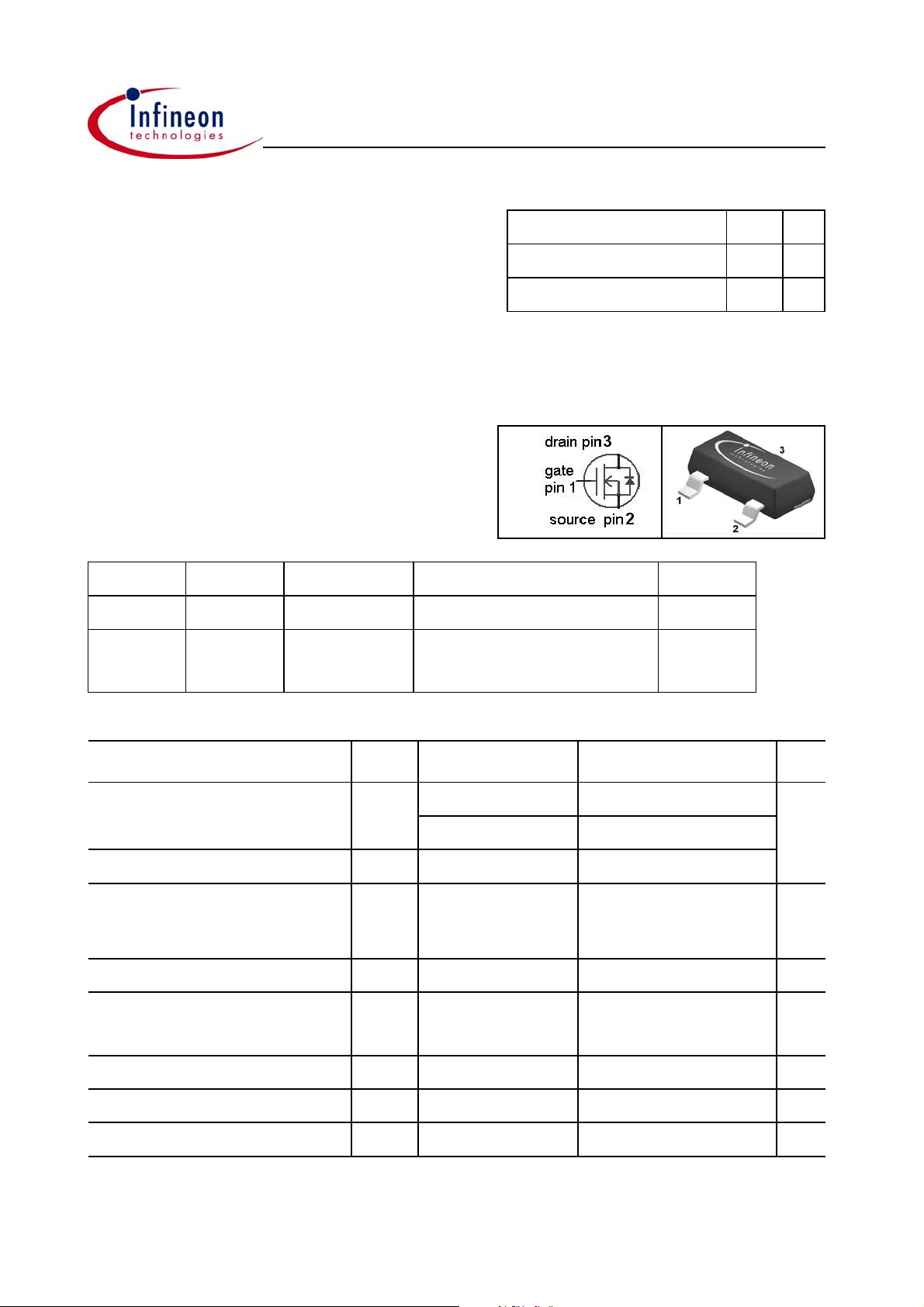
PG-SOT-23
Type Package Ordering Code Tape and Reel Information Marking
0)
BSS139
BSS139
PG-SOT-23 Q62702-S612 E6327: 3000 pcs/reel STs
0)
PG-SOT-23 Q67042-S4296 E6906: 3000 pcs/reel
sorted in V
GS(th)
bands
1)
STs
250 V
30
0.03 A
Ω
Maximum ratings, at T
Parameter Symbol Conditions Unit
Continuous drain current
Pulsed drain current
Reverse diode dv /dt dv /dt
Gate source voltage
ESD sensitivity (HBM) as per
MIL-STD 883
Power dissipation
Operating and storage temperature
=25 °C, unless otherwise specified
j
I
D
I
D,pulse
TA=25 °C
T
=70 °C
A
TA=25 °C
=0.1 A,VDS=200 V,
I
D
di /dt =200 A/µs,
T
=150 °C
j,max
V
GS
P
tot
T
, T
j
TA=25 °C
stg
Value
0.10 A
0.08
0.4
6 kV/µs
±20 V
Class 1
0.36 W
-55 ... 150 °C
IEC climatic category; DIN IEC 68-1 55/150/56
0)
also available as non Pb-free on request
1)
see table on next page and diagram 11
Rev. 1.5 page 1 2006-04-27
BSS139
2)
Parameter Symbol Conditions Unit
Values
min. typ. max.
Thermal characteristics
Thermal resistance,
junction - ambient
Electrical characteristics, at T
R
thJA
=25 °C, unless otherwise specified
j
minimal footprint - - 350 K/W
Static characteristics
Drain-source breakdown voltage
Gate threshold voltage
Drain-source cutoff current
V
(BR)DSSVGS
V
GS(th)
I
D(off)
=-3 V, ID=250 µA
VDS=3 V, ID=56 µA
VDS=250 V,
V
=-3 V, Tj=25 °C
GS
250 - - V
-2.1 -1.4 -1
- - 0.1 µA
V
=250 V,
Gate-source leakage current
On-state drain current
Drain-source on-state resistance
Transconductance
Threshold voltage V
sorted in bands
GS(th)
J
I
I
R
g
V
GSS
DSS
DS(on)
fs
GS(th)
DS
V
=-3 V, Tj=125 °C
GS
VGS=20 V, VDS=0 V
VGS=0 V, VDS=10 V
VGS=0 V, ID=15 mA
V
=10 V,ID=0.1 mA
GS
|VDS|>2|ID|R
I
=0.08 A
D
2)
VDS=3 V, ID=56 µA
DS(on)max
,
--10
- - 10 nA
30 - - mA
- 12.5 30
- 7.8 14
0.060 0.13 - S
-1.2 - -1 V
K -1.35 - -1.15
L -1.5 - -1.3
M -1.65 - -1.45
N -1.8 - -1.6
Ω
Each reel contains transistors out of one band whose identifying letter is printed on the reel label. A specific
band cannot be ordered separately.
Rev. 1.5 page 2 2006-04-27
BSS139
y
Parameter Symbol Conditions Unit
Values
min. typ. max.
namic characteristics
D
Input capacitance
Output capacitance
Reverse transfer capacitance
Turn-on delay time
Rise time
Turn-off delay time
Fall time
C
C
C
t
t
t
t
iss
oss
rss
d(on)
r
d(off)
f
V
=-3 V, VDS=25 V,
GS
f =1 MHz
V
=125 V,
DD
V
=-3...5 V,
GS
I
=0.04 A, R
D
=6 Ω
G
-6076pF
- 6.7 8.4
- 2.6 3.3
- 5.8 8.7 ns
- 5.4 8.1
-2943
- 182 273
Gate Charge Characteristics
Gate to source charge
Gate to drain charge
Gate charge total
Q
gs
=200 V,
V
Q
gd
Q
g
DD
I
=0.04 A,
D
V
=-3 to 5 V
GS
- 0.14 0.21 nC
- 1.3 2.0
- 2.3 3.5
Gate plateau voltage
Reverse Diode
Diode continous forward current
Diode pulse current
Diode forward voltage
Reverse recovery time
Reverse recovery charge
V
plateau
I
S
I
S,pulse
V
SD
t
rr
Q
rr
=25 °C
T
A
VGS=-3 V, IF=0.1 A,
T
=25 °C
j
=50 V, IF=0.04 A,
V
R
di
/dt =100 A/µs
F
- -0.28 - V
- - 0.10 A
- - 0.4
- 0.81 1.2 V
- 8.6 12.9 ns
- 2.1 3.1 nC
Rev. 1.5 page 3 2006-04-27
 Loading...