

INFINEON BSP373N Datasheet
BSP373N
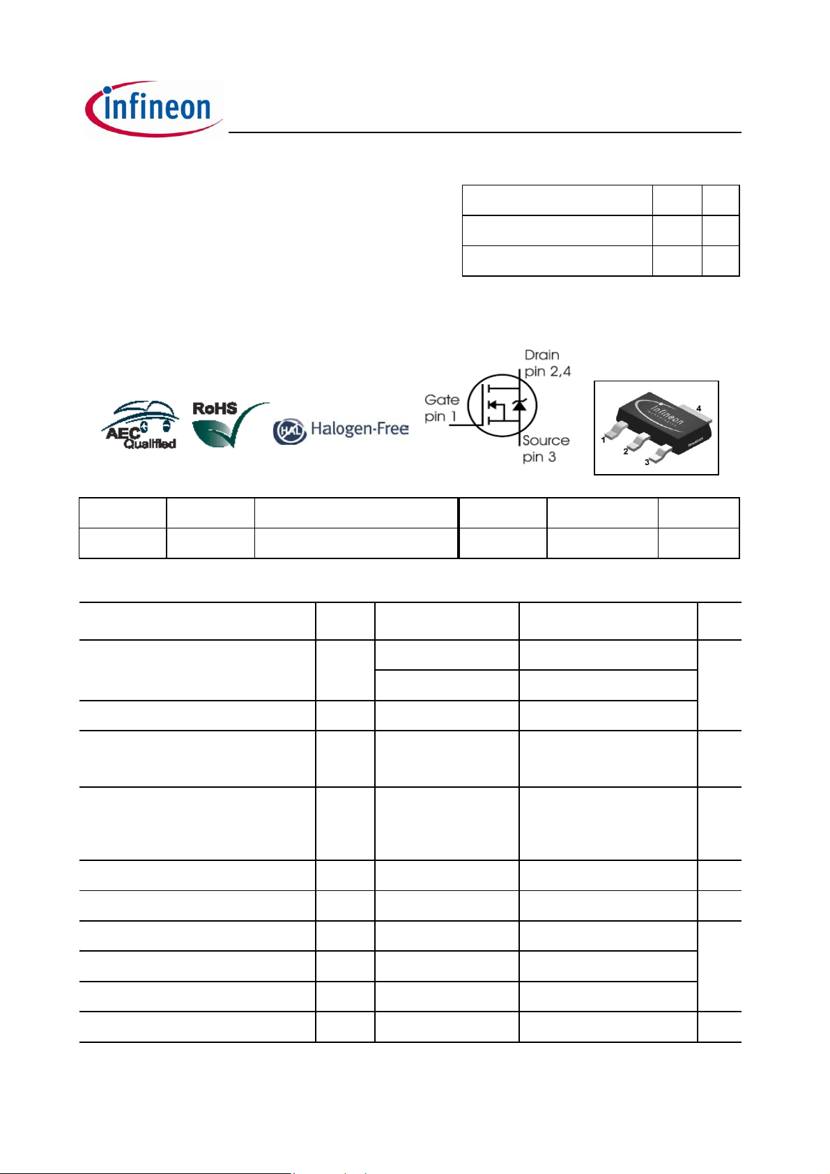
OptiMOS™ Small-Signal-Transistor
Features
• N-channel
• Enhancement mode
• Avalanche rated
• Qualified according to AEC Q101
• 100% lead-free; RoHS compliant
• Halogen-free according to IEC61249-2-21
Maximum ratings, at Tj=25 °C, unless otherwise specified
Parameter Symbol Conditions Unit
Continuous drain current
I
D
TA=25 °C
1.8 A
TA=70 °C
1.5
Pulsed drain current
I
D,pulse
TA=25 °C
7.3
Avalanche energy, single pulse
E
AS
ID=1.8 A, RGS=25 W
33 mJ
Reverse diode dv/dt dv/dt
ID=1.8 A, VDS=80 V,
di/dt=200 A/µs,
T
j,max
=150 °C
6 kV/µs
Gate source voltage
V
GS
±20 V
Power dissipation
1)
P
tot
TA=25 °C
W
Operating and storage temperature
Tj, T
stg
-55 ... 150 °C
ESD Class
JESD22-A114 -HBM 0 (<250V)
Soldering Temperature 260 °C
IEC climatic category; DIN IEC 68-1 55/150/56
Value
1.8
PG-SOT223
Type
Package
Tape and Reel Information
Marking
Halogen-Free
Packing
BSP373N
SOT223
H6327: 1000 pcs/ reel
BSP373N
Yes
Non dry
V
DS
100 V R
DS(on),max
0.24
W
ID 1.8
A
Product Summary
Rev 2.0 page 1 2013-04-04
BSP373N
Parameter Symbol Conditions Unit
min. typ. max.
Thermal characteristics
Thermal resistance
junction - soldering point
R
thJS
- - 25 K/W
Thermal resistance
R
thJA
minimal footprint - - 110
junction - ambient
6 cm2 cooling area
1)
- - 70
Electrical characteristics, at Tj=25 °C, unless otherwise specified
Static characteristics
Drain-source breakdown voltage
V
(BR)DSSVGS
=0 V, ID=250 µA
100 - - V
Gate threshold voltage
V
GS(th)
VDS=Vgs V, ID=218 µA
2.1 3.0 4.0
Drain-source leakage current
I
DSS
VDS=100 V, VGS=0 V,
Tj=25 °C
- - 0.1
mA
VDS=100 V, VGS=0 V,
Tj=150 °C
- - 10
Gate-source leakage current
I
GSS
VGS=20 V, VDS=0 V
- - 10 nA
Drain-source on-state resistance
R
DS(on)
VGS=10 V, ID=1.8 A
- 177 240
mW
Transconductance
g
fs
|VDS|>2|ID|R
DS(on)max
,
ID=1.5 A
3.23 - S
Values
1)
Device on 40mm x 40mm x 1.5mm epoxy PCB FR4 with 6cm² (one layer, 70µm thick) copper area for drain
connection. PCB is vertical in still air.
Rev 2.0 page 2 2013-04-04
BSP373N
Parameter Symbol Conditions Unit
min. typ. max.
Dynamic characteristics
Input capacitance
C
iss
- 199 265 pF
Output capacitance
C
oss
- 36 48
Reverse transfer capacitance
C
rss
- 14 21
Turn-on delay time
t
d(on)
- 4.6 6.9 ns
Rise time
t
r
- 5.9 8.91
Turn-off delay time
t
d(off)
- 21.9 32.9
Fall time
t
f
- 13.5 20.3
Gate Charge Characteristics
Gate to source charge
Q
gs
- 0.8 1.2 nC
Gate to drain charge
Q
gd
- 2.7 4.0
Gate charge total
Q
g
- 6.2 9.3
Gate plateau voltage
V
plateau
- 4.1 - V
Reverse Diode
Diode continous forward current
I
S
- - 1.8 A
Diode pulse current
I
S,pulse
- - 7.3
Diode forward voltage
V
SD
VGS=0 V, IF=1.8 A,
Tj=25 °C
- 0.82 1.1 V
Reverse recovery time
t
rr
- 33 49.5 ns
Reverse recovery charge
Q
rr
- 46 69 nC
VR=50 V, IF=1.8 A,
diF/dt=100 A/µs
TA=25 °C
Values
VGS=0 V, VDS=25 V,
f=1 MHz
VDD=50 V, VGS=10 V,
ID=1.8 A, RG=6 W
VDD=50 V, ID=1.8 A,
VGS=0 to 10 V
Rev 2.0 page 3 2013-04-04
 Loading...