


BSM 200 GA 120 DN2
IGBT Power Module
• Single switch
• Including fast free-wheeling diodes
• Package with insulated metal base plate
Type
V
CE
I
C
Package Ordering Code
BSM 200 GA 120 DN2 1200V 300A SINGLE SWITCH 1 C67076-A2006-A70
BSM 200 GA 120 DN2 S 1200V 300A SSW SENSE 1 C67070-A2006-A70
Maximum Ratings
Parameter
Collector-emitter voltage V
Collector-gate voltage
R
= 20 k
GE
Ω
Gate-emitter voltage V
DC collector current
T
= 25 °C
C
T
= 80 °C
C
Pulsed collector current, tp = 1 ms
T
= 25 °C
C
T
= 80 °C
C
Power dissipation per IGBT
T
= 25 °C
C
Symbol Values Unit
1200 V
V
CE
CGR
1200
GE
I
C
± 20
A
300
200
I
Cpuls
600
400
P
tot
W
1550
Chip temperature T
Storage temperature T
Thermal resistance, chip case R
Diode thermal resistance, chip case R
Insulation test voltage, t = 1min. V
j
stg
thJC
thJC
is
D
+ 150 °C
-40 ... + 125
≤
0.08 K/W
≤ 0.15
2500 Vac
Creepage distance - 20 mm
Clearance - 11
DIN humidity category, DIN 40 040 - F sec
IEC climatic category, DIN IEC 68-1 - 40 / 125 / 56
1 Oct-27-1997

BSM 200 GA 120 DN2
Electrical Characteristics, at Tj = 25 °C, unless otherwise specified
Parameter
Static Characteristics
Gate threshold voltage
V
GE
= V
CE, IC
= 8 mA
Collector-emitter saturation voltage
V
= 15 V, IC = 200 A, Tj = 25 °C
GE
V
= 15 V, IC = 200 A, Tj = 125 °C
GE
Zero gate voltage collector current
V
= 1200 V, VGE = 0 V, Tj = 25 °C
CE
V
= 1200 V, VGE = 0 V, Tj = 125 °C
CE
Gate-emitter leakage current
V
= 20 V, VCE = 0 V
GE
AC Characteristics
Symbol Values Unit
min. typ. max.
V
GE(th)
V
4.5 5.5 6.5
V
CE(sat)
I
CES
I
GES
-
-
-
-
2.5
3.1
3
12
3
3.7
mA
4
nA
- - 200
Transconductance
V
= 20 V, IC = 200 A
CE
Input capacitance
V
= 25 V, VGE = 0 V, f = 1 MHz
CE
Output capacitance
V
= 25 V, VGE = 0 V, f = 1 MHz
CE
Reverse transfer capacitance
V
= 25 V, VGE = 0 V, f = 1 MHz
CE
g
C
C
C
fs
iss
oss
rss
S
108 - -
nF
- 13 -
- 2 -
- 1 -
2 Oct-27-1997

BSM 200 GA 120 DN2
Electrical Characteristics, at Tj = 25 °C, unless otherwise specified
Parameter
Symbol Values Unit
min. typ. max.
Switching Characteristics, Inductive Load at Tj = 125 °C
Turn-on delay time
V
= 600 V, VGE = 15 V, IC = 200 A
CC
R
Gon
= 4.7
Ω
Rise time
V
= 600 V, VGE = 15 V, IC = 200 A
CC
R
Gon
= 4.7
Ω
Turn-off delay time
V
= 600 V, VGE = -15 V, IC = 200 A
CC
R
Goff
= 4.7
Ω
Fall time
V
= 600 V, VGE = -15 V, IC = 200 A
CC
R
Goff
= 4.7
Ω
t
d(on)
t
r
t
d(off)
t
f
- 110 220
- 80 160
- 550 800
- 80 120
ns
Free-Wheel Diode
Diode forward voltage
I
= 200 A, VGE = 0 V, Tj = 25 °C
F
I
= 200 A, VGE = 0 V, Tj = 125 °C
F
Reverse recovery time
I
= 200 A, VR = -600 V, VGE = 0 V
F
di
/dt = -2000 A/µs, Tj = 125 °C
F
Reverse recovery charge
I
= 200 A, VR = -600 V, VGE = 0 V
F
di
/dt = -2000 A/µs
F
T
= 25 °C
j
T
= 125 °C
j
V
t
Q
F
-
-
rr
2.3
1.8
2.8
-
V
µs
- 0.5 -
rr
-
-
12
36
-
-
µC
3 Oct-27-1997
BSM 200 GA 120 DN2
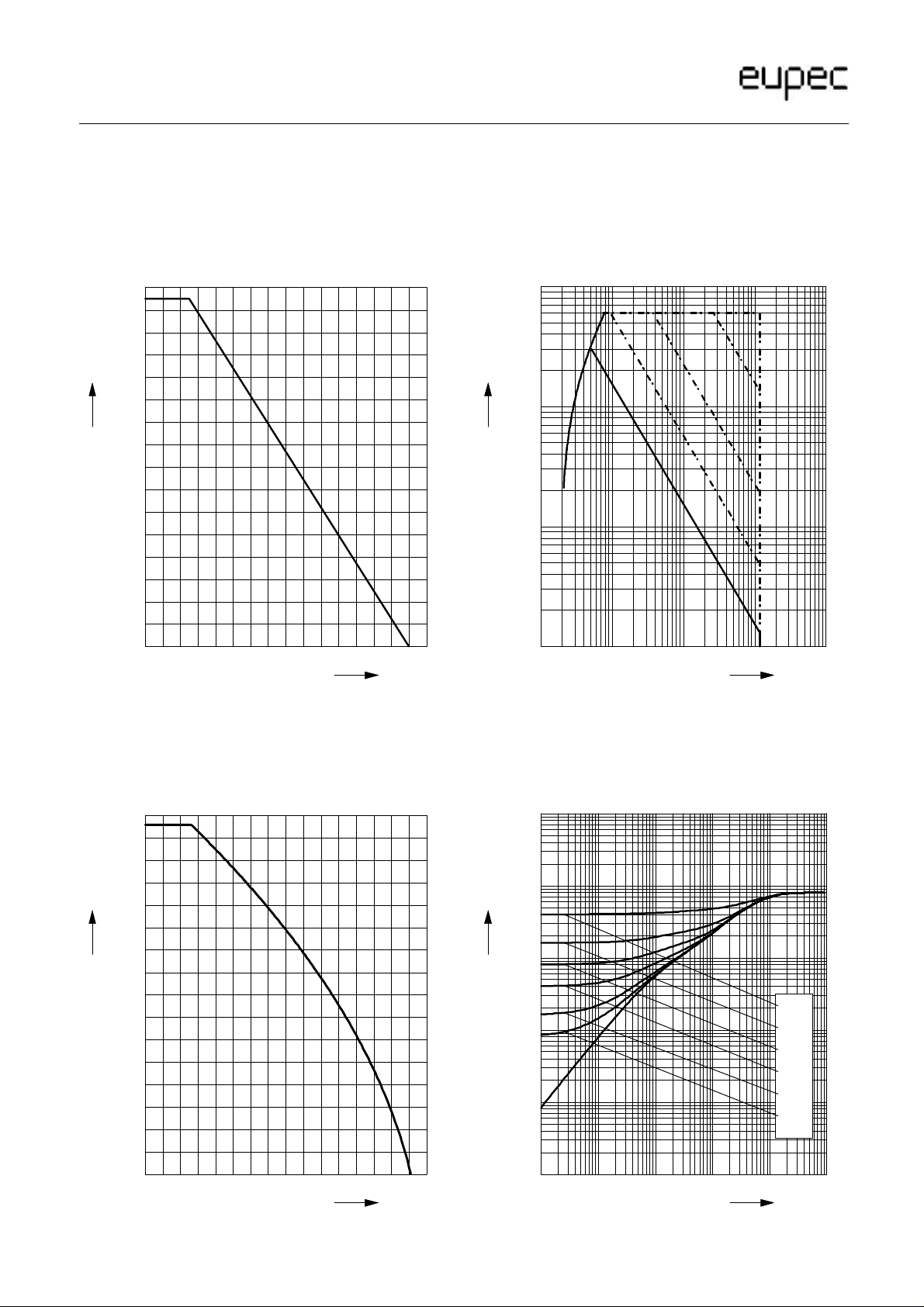
Power dissipation
P
= ƒ(TC)
tot
parameter: T
1600
W
P
tot
1200
1000
800
600
400
200
0
≤ 150 °C
j
0 20 40 60 80 100 120 °C 160
Safe operating area
IC = ƒ(VCE)
parameter: D = 0, TC = 25°C , T
3
10
A
I
C
2
10
1
10
0
10
0
10
T
C
10
1
10
j
2
≤ 150 °C
t
= 21.0µs
p
100 µs
1 ms
10 ms
DC
3
10
V
V
CE
Collector current
IC = ƒ(TC)
parameter: V
320
A
I
C
240
200
160
120
80
40
0
0 20 40 60 80 100 120 °C 160
GE
≥
15 V , T
150 °C
≤
j
Transient thermal impedance IGBT
Z
= ƒ(tp)
th JC
parameter: D = tp / T
0
10
K/W
-1
10
Z
thJC
-2
10
D = 0.50
-3
10
10
-5
single pulse
-4
10
10
-3
10
-2
-4
10
-5
10
T
C
10
-1
t
p
0.20
0.10
0.05
0.02
0.01
10 0 s
4 Oct-27-1997
 Loading...