

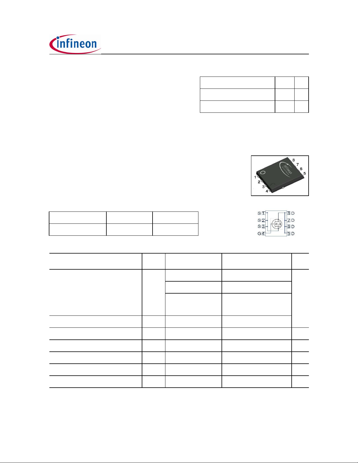
BSC196N10NS G
OptiMOS®2 Power-Transistor
Features
• N-channel, normal level
• Excellent gate charge x R
• Very low on-resistance R
• 150 °C operating temperature
• Pb-free lead plating; RoHS compliant
• Qualified according to JEDEC
• Ideal for high-frequency switching and synchronous rectification
Type Package Marking
BSC196N10NS G PG-TDSON-8 196N10NS
product (FOM)
DS(on)
DS(on)
1)
for target application
Product Summary
V
DS
R
DS(on),max
I
D
100 V
19.6
45 A
PG-TDSON-8
mΩ
Maximum ratings, at T
Parameter Symbol Conditions Unit
Continuous drain current
Pulsed drain current
Avalanche energy, single pulse
Gate source voltage
Power dissipation
Operating and storage temperature
=25 °C, unless otherwise specified
j
I
D
TC=25 °C
T
T
R
3)
I
D,pulse
E
AS
V
GS
P
tot
T
j
, T
TC=25 °C
ID=45 A, RGS=25 Ω
TC=25 °C
stg
=100 °C
C
=25 °C,
A
=45 K/W
thJA
Value
45 A
29
2)
8.5
164
60 mJ
±20 V
78 W
-55 ... 150 °C
IEC climatic category; DIN IEC 68-1 55/150/56
1)
J-STD20 and JESD22
Rev. 1.04 page 1 2008-05-08

BSC196N10NS G
Parameter Symbol Conditions Unit
Values
min. typ. max.
Thermal characteristics
Thermal resistance, junction - case
Thermal resistance,
junction - ambient
Electrical characteristics, at T
=25 °C, unless otherwise specified
j
R
thJC
R
thJA
minimal footprint - - 62
6 cm
2
cooling area
2)
- - 1.6 K/W
--45
Static characteristics
Drain-source breakdown voltage
Gate threshold voltage
Zero gate voltage drain current
V
(BR)DSSVGS
V
GS(th)
I
DSS
=0 V, ID=1 mA
VDS=VGS, ID=42 µA
VDS=100 V, VGS=0 V,
T
=25 °C
j
V
=100 V, VGS=0 V,
DS
T
=125 °C
j
100 - - V
234
- 0.01 1 µA
- 10 100
Gate-source leakage current
Drain-source on-state resistance
Gate resistance
Transconductance
2)
Device on 40 mm x 40 mm x 1.5 mm epoxy PCB FR4 with 6 cm2 (one layer, 70 µm thick) copper area for drain
connection. PCB is vertical in still air.
3)
see figure 3
I
GSS
R
DS(on)VGS
R
G
g
fs
VGS=20 V, VDS=0 V
=10 V, ID=45 A
|VDS|>2|ID|R
I
=45 A
D
DS(on)max
- 1 100 nA
- 16.7 19.6
-1-
,
24 48 - S
mΩ
Ω
Rev. 1.04 page 2 2008-05-08
BSC196N10NS G
g
Parameter Symbol Conditions Unit
Values
min. typ. max.
Dynamic characteristics
Input capacitance
Output capacitance
Reverse transfer capacitance
Turn-on delay time
Rise time
Turn-off delay time
Fall time
Gate Char
e Characteristics
Gate to source charge
Gate to drain charge
Switching charge
Gate charge total
4)
C
C
C
t
t
t
t
Q
Q
Q
Q
iss
oss
rss
d(on)
r
d(off)
f
gs
gd
sw
g
=0 V, VDS=50 V,
V
GS
f =1 MHz
V
=50 V, VGS=10 V,
DD
=25 A, RG=1.6 Ω
I
D
=50 V, ID=25 A,
V
DD
V
=0 to 10 V
GS
- 1700 2300 pF
- 250 330
-1726
-1624ns
-2233
-1828
-58
- 9 12 nC
-69
-1014
-2534
Gate plateau voltage
Output charge
V
Q
plateau
oss
Reverse Diode
Diode continous forward current
Diode pulse current
Diode forward voltage
Reverse recovery time
Reverse recovery charge
4)
See figure 16 for gate charge parameter definition
I
S
I
S,pulse
V
SD
t
rr
Q
rr
VDD=50 V, VGS=0 V
=25 °C
T
C
VGS=0 V, IF=45 A,
T
=25 °C
j
VR=50 V, IF=25 A,
di
/dt =100 A/µs
F
- 5.2 - V
-2735nC
- - 45 A
- - 180
- 1.0 1.3 V
-82-ns
- 199 - nC
Rev. 1.04 page 3 2008-05-08
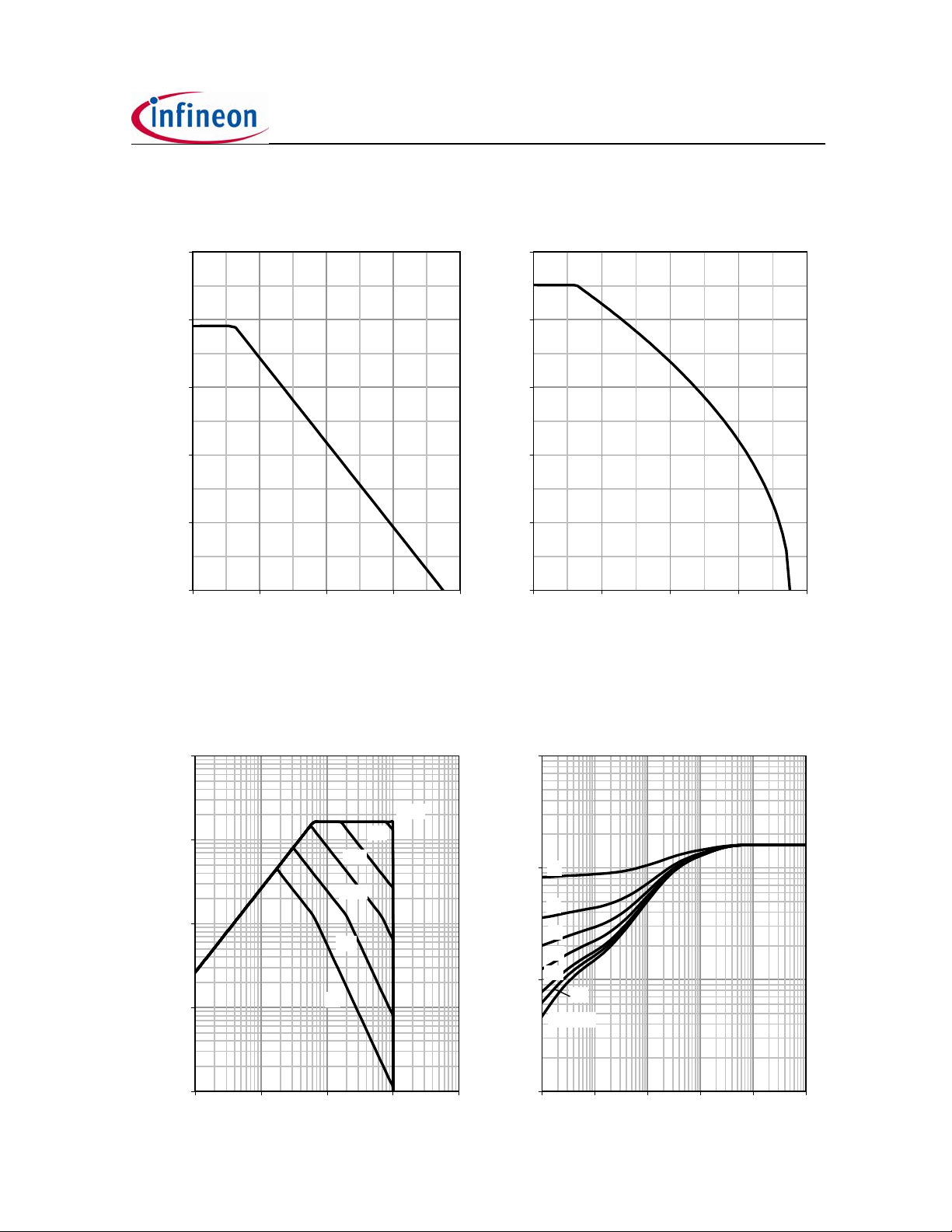
1 Power dissipation 2 Drain current
P
=f(TC) ID=f(TC); VGS≥10 V
tot
BSC196N10NS G
100
80
60
[W]
tot
P
40
20
0
0 40 80 120 160
TC [°C]
50
40
30
[A]
D
I
20
10
0
0 40 80 120 160
TC [°C]
3 Safe operating area 4 Max. transient thermal impedance
I
=f(VDS); TC=25 °C; D =0 Z
D
parameter: t
10
p
3
=f(tp)
thJC
parameter: D =tp/T
1
10
100 ns
1 µs
10 µs
100 µs
1 ms
DC
1
10
2
10
3
10
[K/W]
thJC
Z
10
10
0
-1
-2
10
0.5
0.2
0.1
0.05
0.02
0.01
single pulse
-5
10
10
-3
-4
10
-2
10
-1
10
0
tp [s]
[A]
D
I
10
10
10
10
2
1
0
-1
10
-1
10
0
10
VDS [V]
Rev. 1.04 page 4 2008-05-08
 Loading...