

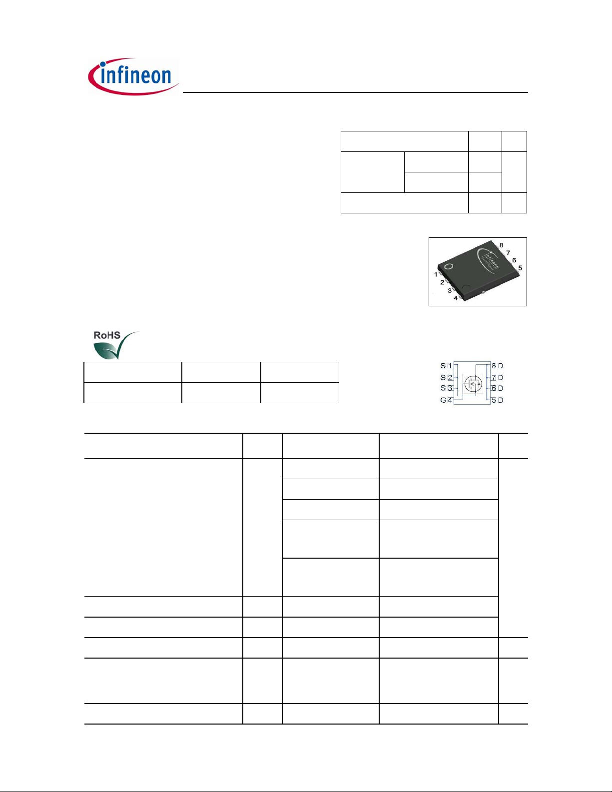
BSC120N03MS G
OptiMOS®3 M-Series Power-MOSFET
Features
• Optimized for 5V driver application (Notebook, VGA, POL)
• Low FOM
• 100% Avalanche tested
• N-channel
• Very low on-resistance R
• Excellent gate charge x R
• Qualified according to JEDEC
• Superior thermal resistance
• Pb-free plating; RoHS compliant
Type Package Marking
BSC120N03MS G PG-TDSON-8 120N03MS
for High Frequency SMPS
SW
@ VGS=4.5 V
DS(on)
product (FOM)
DS(on)
1)
for target applications
Product Summary
V
DS
R
DS(on),max
VGS=10 V 12
VGS=4.5 V 14
I
D
30 V
mΩ
39 A
PG-TDSON-8
Maximum ratings, at T
Parameter Symbol Conditions Unit
Continuous drain current
Pulsed drain current
Avalanche current, single pulse
Avalanche energy, single pulse
Reverse diode dv /dt dv /dt
=25 °C, unless otherwise specified
j
I
D
VGS=10 V, TC=25 °C
V
V
V
T
V
R
3)
4)
I
D,pulse
I
AS
E
AS
TC=25 °C
TC=25 °C
ID=25 A, RGS=25 Ω
I
di /dt =200 A/µs,
T
=10 V, TC=100 °C
GS
=4.5 V, TC=25 °C
GS
=4.5 V,
GS
=100 °C
C
=4.5 V, TA=25 °C,
GS
=50 K/W
thJA
=39 A, VDS=24 V,
D
=150 °C
j,max
2)
Value
39 A
24
36
23
11
156
35
10 mJ
6 kV/µs
Gate source voltage
1)
J-STD20 and JESD22
V
GS
±20 V
Rev. 1.12 page 1 2008-05-30

Maximum ratings, at Tj=25 °C, unless otherwise specified
BSC120N03MS G
Parameter Symbol Conditions Unit
stg
TC=25 °C
=25 °C,
T
A
R
=50 K/W
thJA
2)
Power dissipation
Operating and storage temperature
P
tot
, T
T
j
Value
28 W
2.5
-55 ... 150 °C
IEC climatic category; DIN IEC 68-1 55/150/56
Parameter Symbol Conditions Unit
Values
min. typ. max.
Thermal characteristics
Thermal resistance, junction - case
Device on PCB
Electrical characteristics, at T
=25 °C, unless otherwise specified
j
R
thJC
R
thJA
6 cm2 cooling area
2)
- - 4.5 K/W
--50
Static characteristics
Drain-source breakdown voltage
Gate threshold voltage
Zero gate voltage drain current
Gate-source leakage current
Drain-source on-state resistance
Gate resistance
Transconductance
2)
Device on 40 mm x 40 mm x 1.5 mm epoxy PCB FR4 with 6 cm2 (one layer, 70 µm thick) copper area for drain
connection. PCB is vertical in still air.
3)
See figure 3 for more detailed information
V
(BR)DSSVGS
V
GS(th)
I
DSS
I
GSS
R
DS(on)
R
G
g
fs
=0 V, ID=1 mA
VDS=VGS, ID=250 µA
VDS=30 V, VGS=0 V,
T
=25 °C
j
V
=30 V, VGS=0 V,
DS
T
=125 °C
j
VGS=16 V, VDS=0 V
VGS=4.5 V, ID=20 A
=10 V, ID=30 A
V
GS
|VDS|>2|ID|R
I
=30 A
D
DS(on)max
30 - - V
1-2
- 0.1 1 µA
- 10 100
- 10 100 nA
- 12.5 14
- 10.0 12.0
0.4 0.9 1.6
,
25 50 - S
mΩ
Ω
Rev. 1.12 page 2 2008-05-30
BSC120N03MS G
g
Parameter Symbol Conditions Unit
Values
min. typ. max.
Dynamic characteristics
Input capacitance
Output capacitance
Reverse transfer capacitance
Turn-on delay time
Rise time
Turn-off delay time
Fall time
Gate Char
e Characteristics
Gate to source charge
Gate charge at threshold
Gate to drain charge
Switching charge
C
iss
=0 V, VDS=15 V,
V
C
oss
C
rss
t
d(on)
t
r
t
d(off)
t
f
5)
Q
gs
Q
g(th)
Q
gd
Q
sw
GS
f =1 MHz
V
=15 V, VGS=4.5 V,
DD
=30 A, RG=1.6 Ω
I
D
=15 V, ID=30 A,
V
DD
V
=0 to 4.5 V
GS
- 1100 1500 pF
- 390 520
-24-
- 7.9 - ns
- 4.4 -
- 7.0 -
- 5.0 -
- 3.8 5.1 nC
- 1.8 2.4
- 1.7 2.9
- 3.7 5.5
Gate charge total
Gate plateau voltage
Gate charge total
Gate charge total, sync. FET
Output charge
Q
V
Q
Q
Q
g
plateau
g
g(sync)
oss
Reverse Diode
Diode continuous forward current
Diode pulse current
Diode forward voltage
Reverse recovery charge
4)
See figure 13 for more detailed information
5)
See figure 16 for gate charge parameter definition
I
S
I
S,pulse
V
SD
Q
rr
VDD=15 V, ID=30 A,
V
=0 to 10 V
GS
VDS=0.1 V,
V
=0 to 4.5 V
GS
VDD=15 V, VGS=0 V
TC=25 °C
VGS=0 V, IF=30 A,
T
=25 °C
j
VR=15 V, IF=IS,
di
/dt =400 A/µs
F
- 7.2 10
- 3.3 - V
-1520
- 6.2 8.3 nC
-1014
- - 25 A
- - 156
- 0.92 1.1 V
- - 10 nC
Rev. 1.12 page 3 2008-05-30
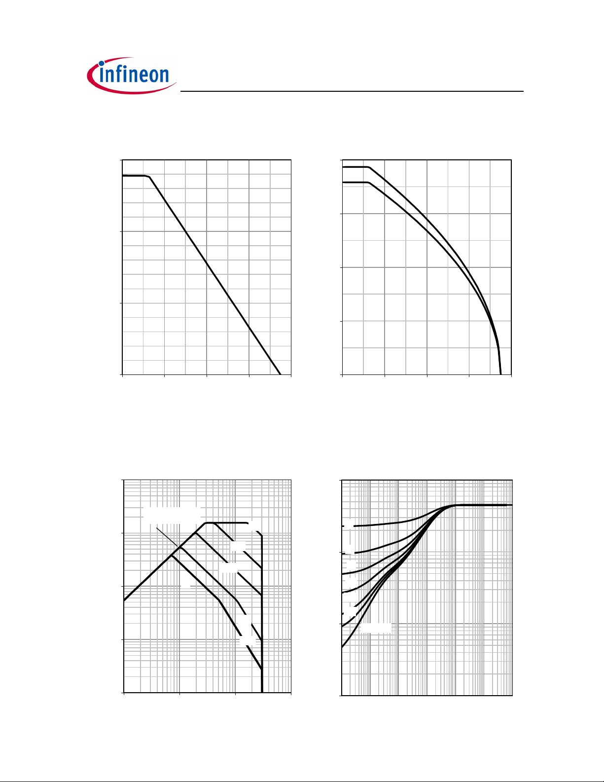
1 Power dissipation 2 Drain current
P
=f(TC) ID=f(TC)
tot
parameter: V
GS
BSC120N03MS G
[W]
tot
P
30
20
[A]
D
I
40
30
20
10 V
4.5 V
10
10
0
0 40 80 120 160
TC [°C]
0
0 40 80 120 160
TC [°C]
3 Safe operating area 4 Max. transient thermal impedance
I
=f(VDS); TC=25 °C; D =0 Z
D
parameter: t
10
p
3
=f(tp)
thJC
parameter: D =tp/T
10
limited by on-state
[A]
D
I
10
10
10
10
resistance
2
10
DC
0
1
0
-1
-1
10
100 µs
10 µs
10
1 ms
10 ms
1
1 µs
10
2
VDS [V]
0.5
0.2
1
0.1
0.05
[K/W]
0.02
thJC
Z
0.01
0.1
0.01
single pulse
0000001
10
-5
-6
10
10
-3
-4
10
10
-1
-2
10
tp [s]
10
0
Rev. 1.12 page 4 2008-05-30
 Loading...