

INFINEON BFR93AW User Manual
NPN Silicon RF Transistor*
j
A
g
• For low distortionbroadband amplifiers and
BFR93AW
oscillators up to 2 GHz at collector currents from
5 mA to 30 mA
3
2
1
* Short term description
ESD (Electrostatic discharge) sensitive device, observe handling precaution!
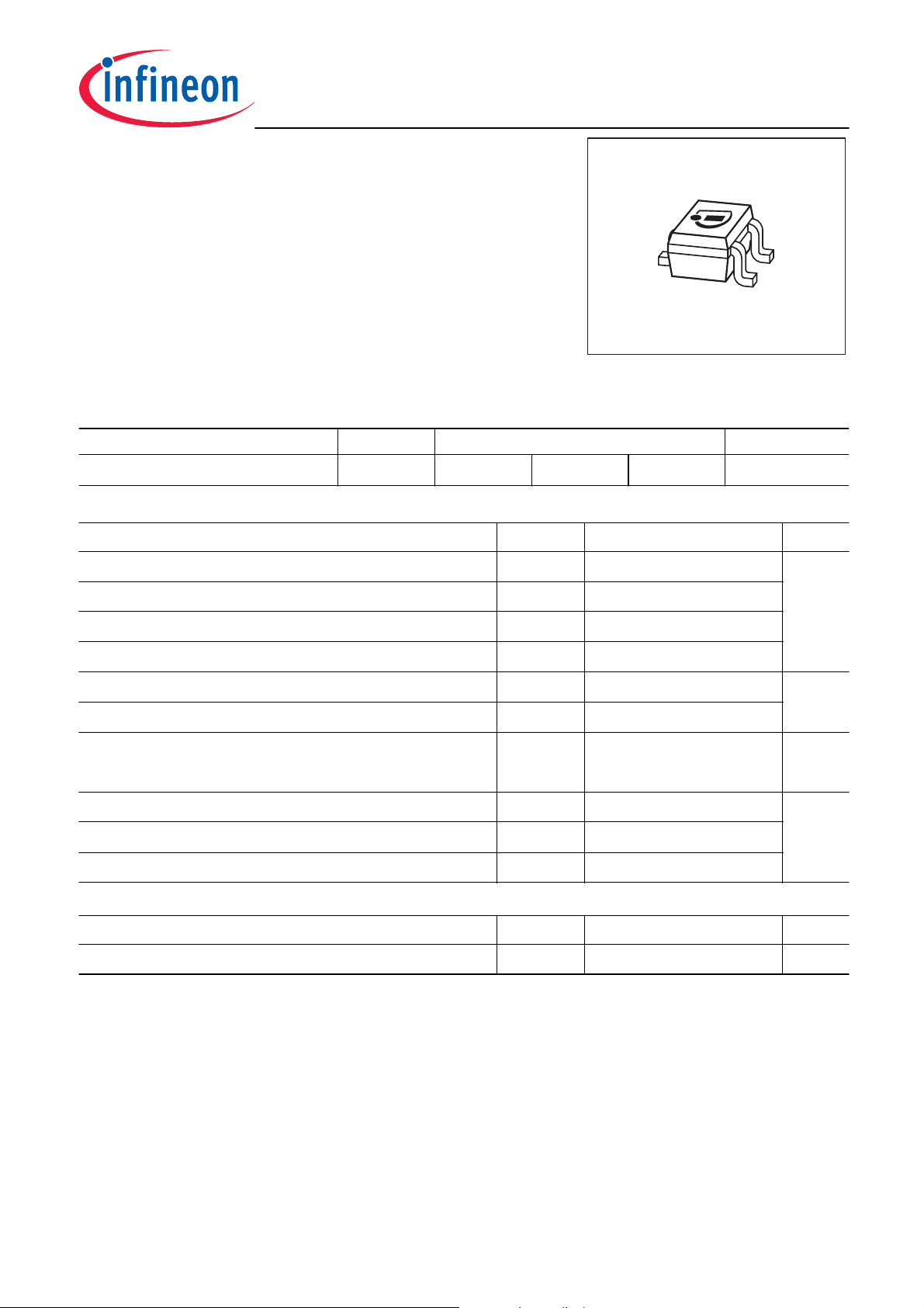
Type Marking Pin Configuration Package
BFR93AW R2s
1=B 2=E 3=C
SOT323
Maximum Ratings
Parameter Symbol Value Unit
Collector-emitter voltage V
Collector-emitter voltage V
Collector-base voltage V
Emitter-base voltage V
Collector current I
Base current I
Total power dissipation1)
P
CEO
CES
CBO
EBO
C
B
tot
12 V
20
20
2
90 mA
9
300 mW
TS ≤ 104 °C
Junction temperature T
Ambient temperature T
Storage temperature T
st
150 °C
-65 ... 150
-65 ... 150
Thermal Resistance
Parameter Symbol Value Unit
Junction - soldering point
1
TS is measured on the collector lead at the soldering point to the pcb
2
For calculation of R
thJA
2)
please refer to Application Note Thermal Resistance
R
thJS
1
≤ 155
K/W
2005-09-30

Electrical Characteristics at TA = 25°C, unless otherwise specified
BFR93AW
Parameter
DC Characteristics
Collector-emitter breakdown voltage
= 1 mA, IB = 0
I
C
Collector-emitter cutoff current
= 20 V, VBE = 0
V
CE
Collector-base cutoff current
= 10 V, IE = 0
V
CB
Emitter-base cutoff current
= 2.5 V, IC = 0
V
EB
DC current gain-
= 30 mA, VCE = 8 V, pulse measured
I
C
Symbol Values Unit
min. typ. max.
V
(BR)CEO
I
CES
I
CBO
I
EBO
h
FE
12 - - V
- - 100 µA
- - 100 nA
- - 10 µA
70 100 140 -
2
2005-09-30

BFR93AW
Electrical Characteristics at T
= 25°C, unless otherwise specified
Parameter
AC Characteristics (verified by random sampling)
Transition frequency
= 15 mA, VCE = 8 V, f = 500 MHz
I
C
Collector-base capacitance
= 10 V, f = 1 MHz, VBE = 0 ,
V
CB
emitter grounded
Collector emitter capacitance
= 10 V, f = 1 MHz, VBE = 0 ,
V
CE
base grounded
Emitter-base capacitance
= 0.5 V, f = 1 MHz, VCB = 0 ,
V
EB
collector grounded
Noise figure
Symbol Values Unit
min. typ. max.
f
T
C
cb
C
ce
C
eb
F
4.5 6 - GHz
- 0.58 0.8 pF
- 0.3 -
- 1.9 -
dB
= 5 mA, VCE = 8 V, ZS = Z
I
C
Sopt
,
f = 900 MHz
= 5 mA, VCE = 8 V, ZS = Z
I
C
Sopt
,
f = 1.8 GHz
Power gain, maximum available1)
= 30 mA, VCE = 8 V, ZS = Z
I
C
Sopt
, ZL = Z
f = 900 MHz
= 30 mA, VCE = 8 V, ZS = Z
I
C
Sopt
, ZL = Z
f = 1.8 GHz
Transducer gain
= 30 mA, VCE = 8 V, ZS = ZL = 50 Ω,
I
C
f = 900 MHz
= 30 mA, VCE = 8 V, ZS = ZL = 50 Ω,
I
C
f = 1.8 MHz
1
G
ma
= |S
21e
/ S
| (k-(k²-1)
12e
1/2
),
Lopt
Lopt
,
,
G
|S
ma
21e
-
-
-
-
2
|
-
-
1.5
2.6
15.5
10.5
13
7.5
-
-
-
dB
-
-
3
2005-09-30
 Loading...