

BFR380F
1
2
3
j
A
g
NPN Silicon RF Transistor
Preliminary data
High current capability and low figure for
wide dynamic range application
Low voltage operation
Ideal for low phase noise oscillators up to 3.5 GHz
Low noise figure: 1.1 dB at 1.8 GHz
ESD: Electrostatic discharge sensitive device, observe handling precaution!
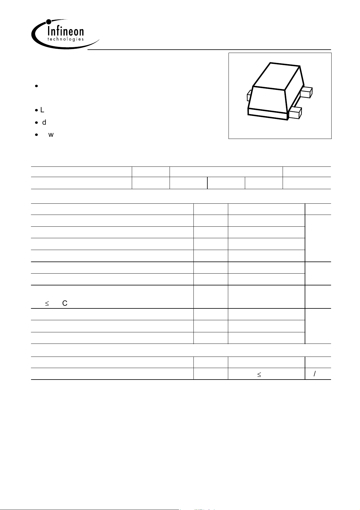
Type Marking Pin Configuration Package
BFR380F FCs
Maximum Ratings
Parameter Symbol Value Unit
Collector-emitter voltage V
Collector-emitter voltage V
Collector-base voltage V
Emitter-base voltage V
Collector current I
Base current I
Total power dissipation1)
T
95°C
S
Junction temperature T
Ambient temperature T
Storage temperature T
Thermal Resistance
1 = B 2 = E 3 = C
CEO
CES
CBO
EBO
C
B
P
tot
st
380 mW
150 °C
-65 ... 150
-65 ... 150
6 V
15
15
2
80 mA
14
TSFP-3
Parameter Symbol Value Unit
Junction - soldering point
1
TS is measured on the collector lead at the soldering point to the pcb
2
For calculation of R
thJA
2)
please refer to Application Note Thermal Resistance
R
thJS
1
145
Jan-24-2003
K/W

Electrical Characteristics at TA = 25°C, unless otherwise specified
BFR380F
Parameter
Characteristics
Collector-emitter breakdown voltage
I
= 1 mA, IB = 0
C
Collector-base cutoff current
V
= 5 V, IE = 0
CB
Emitter-base cutoff current
V
= 1 V, IC = 0
EB
DC current gain-
I
= 40 mA, VCE = 3 V
C
Symbol Values Unit
min. typ. max.
V
(BR)CEO
I
CBO
I
EBO
h
FE
6 9 - V
- - 100 nA
- - 1 µA
60 100 200 -
2
Jan-24-2003
BFR380F
A
Electrical Characteristics at T
= 25°C, unless otherwise specified
Parameter Symbol Values Unit
min. typ. max.
AC Characteristics (verified by random sampling)
Transition frequency
I
= 40 mA, VCE = 3 V, f = 1 GHz
C
Collector-base capacitance
V
= 5 V, f = 1 MHz, emitter grounded
CB
Collector emitter capacitance
V
= 5 V, f = 1 MHz, base grounded
CE
Emitter-base capacitance
V
= 0.5 V, f = 1 MHz, collector grounded
EB
Noise figure
I
= 8 mA, VCE = 3 V, ZS = Z
C
Sopt
,
f
C
C
C
F
T
cb
ce
eb
min
11 14 - GHz
- 0.47 0.7 pF
- 0.2 -
- 1 -
- 1.1 - dB
f = 1.8 GHz
Power gain, maximum available1)
I
= 40 mA, VCE = 3 V, ZS = Z
C
Z
= Z
L
I
= 40 mA, VCE = 3 V, ZS = Z
C
Z
= Z
L
, f = 1.8 GHz
Lopt
, f = 3 GHz
Lopt
Sopt
Sopt
,
,
Insertion power gain
V
= 3 V, IC = 40 mA, f = 1.8 GHz,
CE
Z
= ZL = 50
S
V
= 3 V, IC = 40 mA, f = 3 GHz,
CE
Z
= ZL = 50
S
Third order intercept point at output2)
V
= 3 V, IC = 40 mA, f = 1.8 GHz,
CE
Z
= ZL = 50
S
1dB Compression point at output3)
I
= 40 mA, VCE = 3 V, ZS = ZL = 50 ,
C
f = 1.8 GHz
G
ma
|S21|
IP
3
P
-1dB
-
-
2
-
-
13.5
9
11
6.5
-
-
dB
-
-
- 29 - dBm
- 16 -
1
G
= |S21 / S12| (k-(k²-1)
ma
2
IP3 value depends on termination of all intermodulation frequency components.
Termination used for this measurement is 50
3
DC current at no input power
1/2
)
from 0.1 MHz to 6 GHz
3
Jan-24-2003
 Loading...