

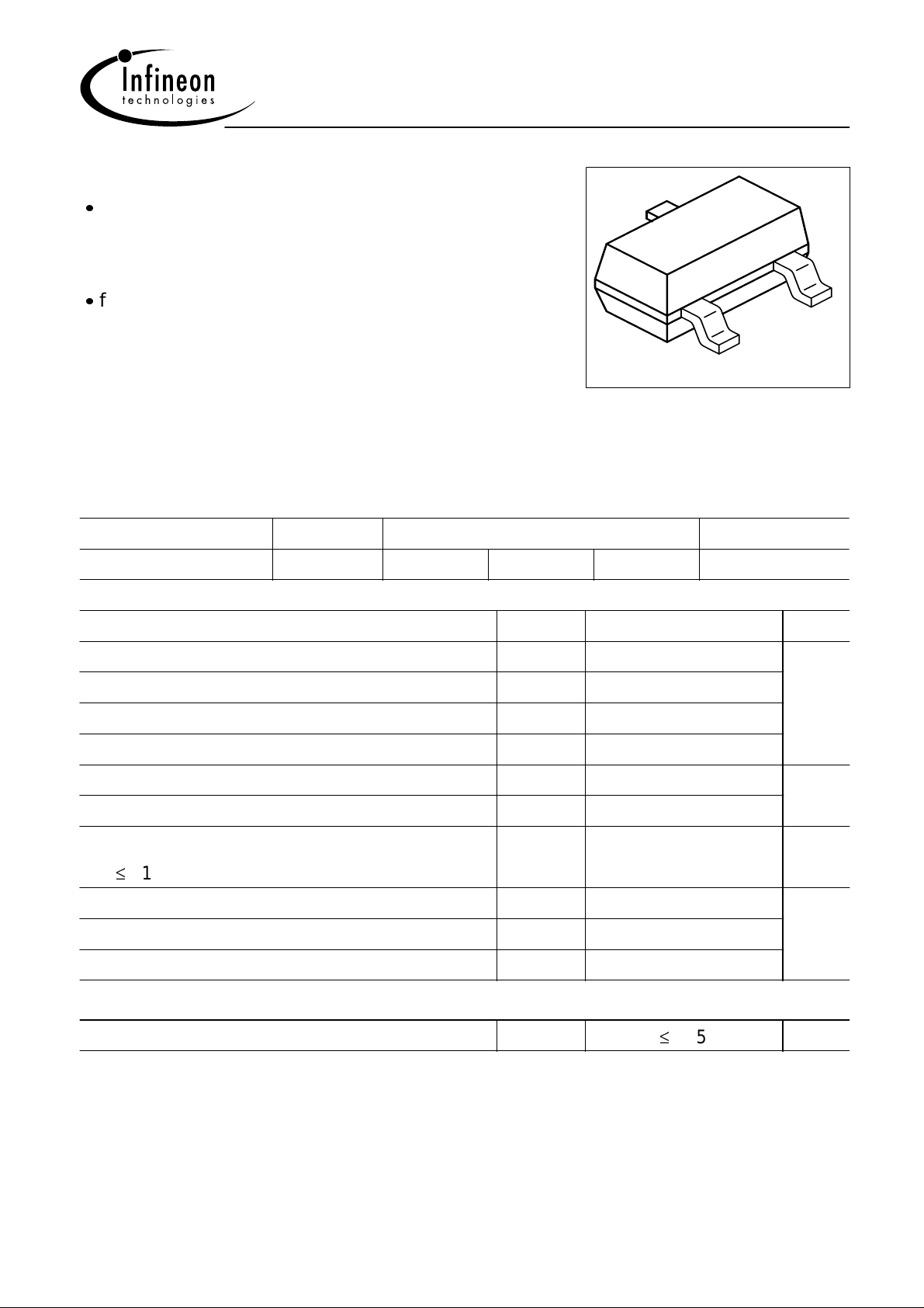
NPN Silicon RF Transistor
m
BFR280
3
For low noise, low-power amplifiers in mobile
communications systems (pager, cordless
telephone) at collector currents from 0.2 mA to 8
fT = 7.5 GHz
F = 1.5 dB at 900 MHz
1
VPS05161
ESD: Electrostatic discharge sensitive device, observe handling precaution!
Type Marking Pin Configuration Package
BFR280 REs 1 = B 2 = E 3 = C SOT23
Maximum Ratings
Parameter Symbol Value Unit
2
Collector-emitter voltage V
Collector-emitter voltage V
Collector-base voltage V
Emitter-base voltage V
Collector current I
Base current I
Total power dissipation
T
116 °C
S
1)
Junction temperature T
Ambient temperature T
Storage temperature T
Thermal Resistance
Junction - soldering point
1
T
is measured on the collector lead at the soldering point to the pcb
S
2
For calculation of R
thJA
2)
please refer to Application Note Thermal Resistance
C
B
P
R
CEO
CES
CBO
EBO
tot
j
A
stg
thJS
8 V
10
10
2
10 mA
1.2
80 mW
150 °C
-65 ... 150
-65 ... 150
425
K/W
Jun-27-20011
Electrical Characteristics at TA = 25°C, unless otherwise specified.
BFR280
Parameter
DC characteristics
Collector-emitter breakdown voltage
I
= 1 mA, IB = 0
C
Collector-emitter cutoff current
= 10 V, VBE = 0
V
CE
Collector-base cutoff current
= 8 V, IE = 0
V
CB
Emitter-base cutoff current
= 1 V, IC = 0
V
EB
DC current gain
= 3 mA, VCE = 5 V
I
C
Symbol Values Unit
min. typ. max.
V
(BR)CEO
I
CES
I
CBO
I
EBO
h
FE
8 - - V
- - 100 µA
- - 100 nA
- - 1 µA
30 100 200
-
Jun-27-20012
BFR280
Electrical Characteristics at T
= 25°C, unless otherwise specified.
A
Parameter
AC characteristics (verified by random sampling)
Transition frequency
I
= 6 mA, VCE = 5 V, f = 500 MHz
C
Collector-base capacitance
V
= 5 V, f = 1 MHz
CB
Collector-emitter capacitance
V
= 5 V, f = 1 MHz
CE
Emitter-base capacitance
V
= 0.5 V, f = 1 MHz
EB
Noise figure
I
= 1.5 mA, VCE = 5 V, ZS = Z
C
Sopt
,
f = 900 MHz
Symbol Values Unit
min. typ. max.
f
C
C
C
F
T
cb
ce
eb
5 7.5 - GHz
- 0.27 0.45 pF
- 0.18 -
- 0.22 -
-
1.5
dB
-
f = 1.8 GHz
Power gain, maximum stable 1)
I
= 3 mA, VCE = 5 V, ZS = Z
C
Sopt
, ZL = Z
f = 900 MHz
f = 1.8 GHz
Transducer gain
I
= 3 mA, VCE = 5 V, ZS = ZL = 50 ,
C
f = 900 MHz
f = 1.8 GHz
1
Gms = |S21 / S12|
Lopt
,
G
|S
ms
21e
-
-
-
2
|
-
-
2
17
11.5
13
8
-
-
-
-
-
Jun-27-20013
 Loading...