

Infineon BFP450 Schematic [ru]
NPN Silicon RF Transistor
z
j
A
g
• For medium power amplifiers
• Compression point P
maximum available gain G
= +19 dBm at 1.8 GHz
-1dB
= 15.5 dB at 1.8 GH
ma
Noise figure F = 1.25 dB at 1.8 GHz
• Transition frequency fT = 24 GHz
• Gold metallization for high reliability
• SIEGET 25 GHz fT - Line
• Pb-free (RoHS compliant) package
• Qualified according AEC Q101
1)
4
BFP450
3
2
1
ESD (Electrostatic discharge) sensitive device, observe handling precaution!
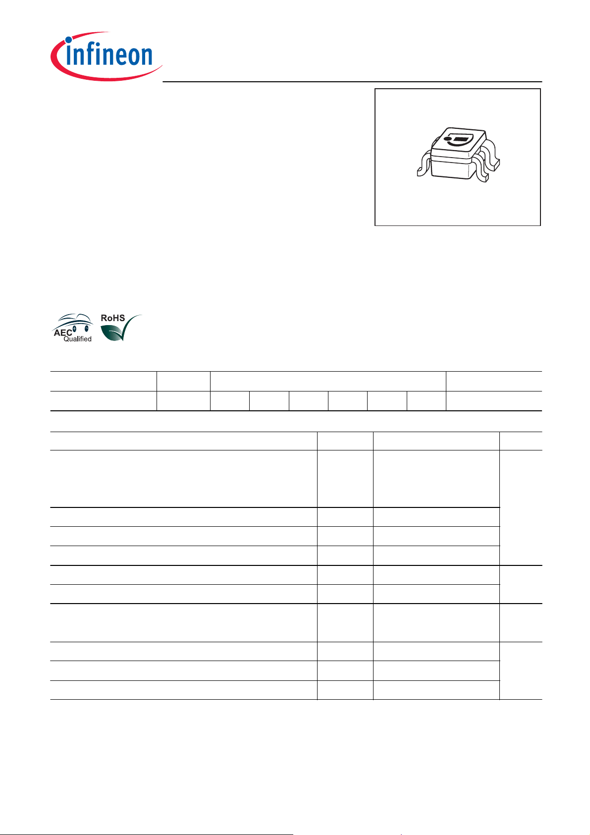
Type Marking Pin Configuration Package
BFP450 ANs
1=B 2=E 3=C 4=E - - SOT343
Maximum Ratings
Parameter Symbol Value Unit
Collector-emitter voltage
V
TA > 0 °C
TA ≤ 0 °C
Collector-emitter voltage V
Collector-base voltage V
Emitter-base voltage V
Collector current I
Base current I
Total power dissipation2)
P
CEO
CES
CBO
EBO
C
B
tot
4.5
4.1
15
15
1.5
100 mA
10
450 mW
V
TS ≤ 96 °C
Junction temperature T
Ambient temperature T
Storage temperature T
1
Pb-containing package may be available upon special request
2
TS is measured on the collector lead at the soldering point to the pcb
st
150 °C
-65 ... 150
-65 ... 150
2007-04-20
1

BFP450
Thermal Resistance
Parameter Symbol Value Unit
Junction - soldering point
1)
R
thJS
Electrical Characteristics at TA = 25°C, unless otherwise specified
≤ 120
K/W
Parameter
DC Characteristics
Collector-emitter breakdown voltage
= 1 mA, IB = 0
I
C
Collector-emitter cutoff current
= 15 V, VBE = 0
V
CE
Collector-base cutoff current
= 5 V, IE = 0
V
CB
Emitter-base cutoff current
= 0.5 V, IC = 0
V
EB
DC current gain
= 50 mA, VCE = 4 V, pulse measured
I
C
1
For calculation of R
please refer to Application Note Thermal Resistance
thJA
Symbol Values Unit
min. typ. max.
V
(BR)CEO
I
CES
I
CBO
I
EBO
h
FE
4.5 5 - V
- - 10 µA
- - 100 nA
- - 10 µA
60 95 130 -
2007-04-20
2

BFP450
Electrical Characteristics at T
= 25°C, unless otherwise specified
Parameter
AC Characteristics (verified by random sampling)
Transition frequency
= 90 mA, VCE = 3 V, f = 1 GHz
I
C
Collector-base capacitance
= 2 V, f = 1 MHz, VBE = 0 ,
V
CB
emitter grounded
Collector emitter capacitance
= 2 V, f = 1 MHz, VBE = 0 ,
V
CE
base greunded
Emitter-base capacitance
= 0.5 V, f = 1 MHz, VCB = 0 ,
V
EB
collector grounded
Noise figure
Symbol Values Unit
min. typ. max.
f
C
C
C
F
T
cb
ce
eb
18 24 - GHz
- 0.48 0.8 pF
- 1.2 -
- 1.75 -
- 1.25 - dB
= 10 mA, VCE = 2 V, f = 1.8 GHz, ZS = Z
I
C
Power gain, maximum available1)
= 50 mA, VCE = 2 V, ZS = Z
I
C
Sopt, ZL
= Z
Sopt
Lopt
,
G
ma
f = 1.8 GHz
Insertion power gain
= 2 V, IC = 50 mA, f = 1.8 GHz,
V
CE
= ZL = 50 Ω
Z
S
Third order intercept point at output2)
= 3 V, IC = 50 mA, f = 1.8 GHz,
V
CE
= ZL = 50 Ω
Z
S
1dB Compression point at output
= 50 mA, VCE = 3 V, ZS = ZL = 50 Ω,
I
C
|S21|
IP
3
P
-1dB
2
f = 1.8 GHz
1
= |
G
ma
2
IP3 value depends on termination of all intermodulation frequency components.
Termination used for this measurement is 50
S
21e
/
S
12e
| (k-(k²-1)
1/2
)
Ω from 0.1 MHz to 6 GHz
- 15.5 -
8 11.5 - dB
- 29 - dBm
- 19 -
2007-04-20
3
SPICE Parameter (Gummel-Poon Model, Berkley-SPICE 2G.6 Syntax):
C
Transistor Chip Data:
BFP450
IS =
VAF =
NE =
VAR =
NC =
RBM =
CJE =
TF =
ITF =
VJC =
TR =
MJS =
XTI =
0.13125 fA
24.165 V
1.5563 -
13.461 V
0.70543 -
2.1659
Ω
3.2276 fF
7.5068 ps
0.017655 mA
1.1487 V
2.6912 ns
03-
BF = 76.123
IKF = 0.58905
BR = 21.254
IKR = 0.25878
RB = 5.403 Ω
RE = 0.45346
VJE = 0.95292
XTF = 0.69972
PTF = 0
MJC = 0.50644
CJS = 0
XTB = 0
FC = 0.91274
A
A
V
deg
F
-
NF =
ISE =
NR =
ISC =
IRB =
RC =
MJE =
VTF =
CJC =
XCJC =
VJS =
EG =
TNOM
0.79652 28341 fA
1.2966 -
0.012292 fA
0.013181 mA
0.50084
Ω
0.48672 -
0.66148 V
1049.5 fF
0.28285 -
0.75 V
1.11 eV
300 K
C`-E`-dioden Data (Berkley-Spice 1G.6 Syntax): IS = 25 fA; N = 1.05 -, RS = 5 Ω
All parameters are ready to use, no scalling is necessary.
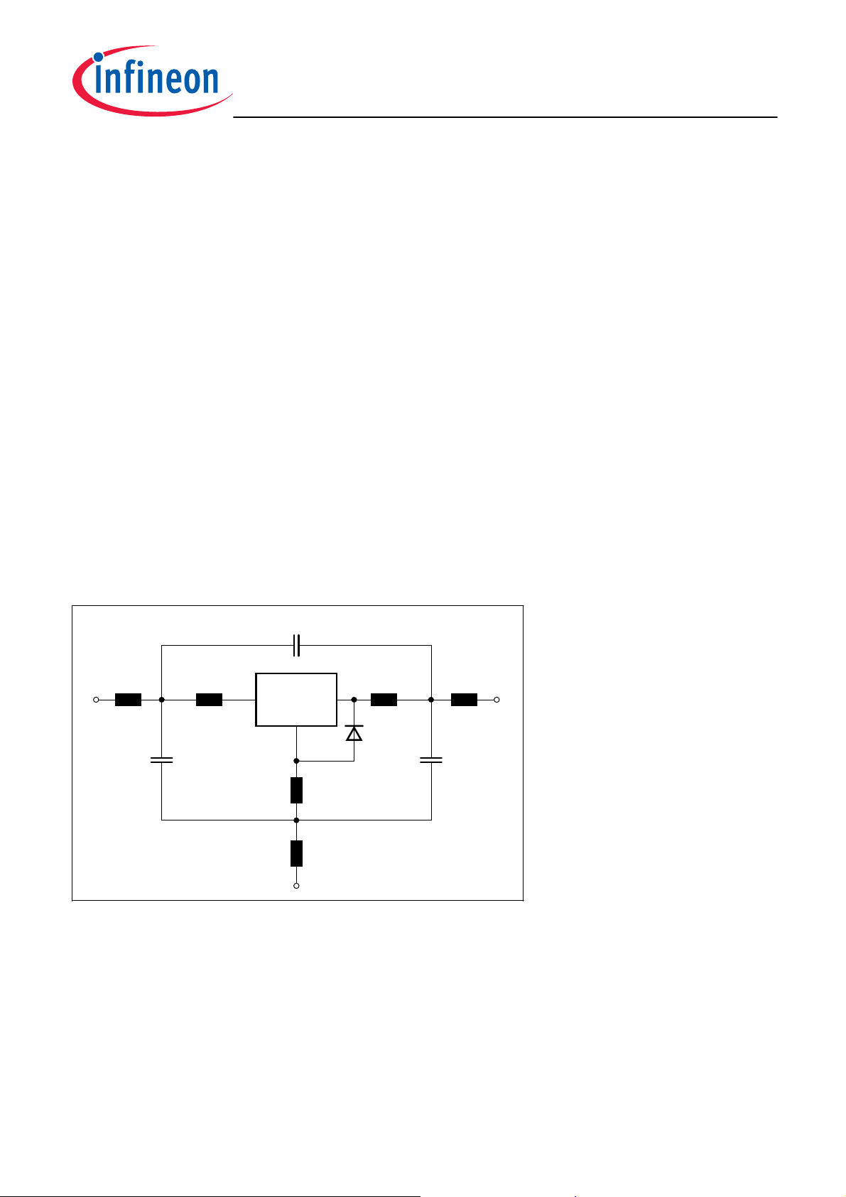
Package Equivalent Circuit:
L
=
C
CB
L
B
BO
L
BI
C
BE
Transistor
Chip
E’
L
EI
L
EO
L
CI
C’B’
C’-E’Diode
L
CO
C
C
CE
BI
=
L
BO
=
L
EI
= 0.05 nH
L
EO
= 0.29 nH
L
CI
= 0.68 nH
L
CO
=
C
BE
=
C
CB
=
C
E
Valid up to 6GHz
0.31
0.63
0.2
208
3.2
213
nH
nH
nH
fF
fF
fF
E
The SOT343 package has two emitter leads. To avoid high complexity to the package equivalent
circuit both leads are combined in one electrical connection
Extracted on behalf of Infineon Technologies AG by: Institut für Mobil- und Satellitentechnik (IMST)
For examples and ready to use parameters please contact your local Infineon Technologies distributor
or sales office to obtain a InfineonTechnologies CD-ROM or see Internet: http//www.infineon.com/silicondiscretes
EHA07389
2007-04-20
4
 Loading...