

INFINEON BFG235 User Manual
NPN Silicon RF Transistor*
j
A
g
• For low-distortion broadband output amplifier
BFG235
stages in antenna and telecommunication
systems up to 2 GHz at collector currents from
120 mA to 250 mA
4
2
1
• Power amplifiers for DECT and PCN systems
• Integrated emitter ballast resistor
• f
= 5.5 GHz
T
* Short term description
ESD (Electrostatic discharge) sensitive device, observe handling precaution!
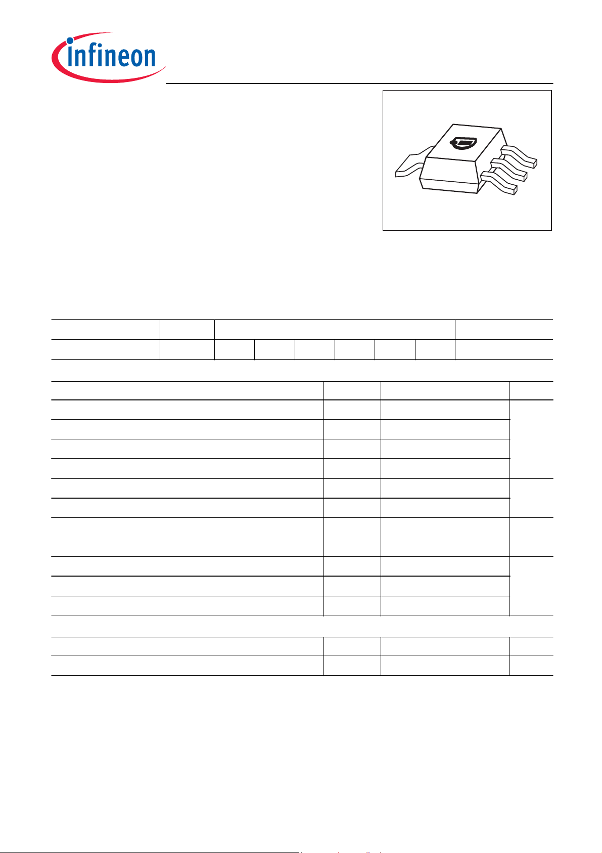
Type Marking Pin Configuration Package
BFG235 BFG235
1 = E 2 = B 3 = E 4 = C - - SOT223
Maximum Ratings
Parameter Symbol Value Unit
Collector-emitter voltage V
Collector-emitter voltage V
Collector-base voltage V
Emitter-base voltage V
Collector current I
Base current I
Total power dissipation1)
P
CEO
CES
CBO
EBO
C
B
tot
15 V
25
25
2
300 mA
40
2 W
TS ≤ 80°C
3
Junction temperature T
Ambient temperature T
Storage temperature T
st
150 °C
-65 ... 150
-65 ... 150
Thermal Resistance
Parameter Symbol Value Unit
Junction - soldering point
1
TS is measured on the collector lead at the soldering point to the pcb
2
For calculation of R
thJA
2)
please refer to Application Note Thermal Resistance
R
thJS
≤ 35
K/W
2005-10-11
1

BFG235
A
Electrical Characteristics at T
= 25°C, unless otherwise specified
Parameter Symbol Values Unit
min. typ. max.
DC Characteristics
Collector-emitter breakdown voltage
I
= 1 mA, IB = 0
C
Collector-emitter cutoff current
V
= 25 V, VBE = 0
CE
Collector-base cutoff current
V
= 10 V, IE = 0
CB
Emitter-base cutoff current
V
= 1 V, IC = 0
EB
DC current gain-
I
= 200 mA, VCE = 8 V, pulse measured
C
V
(BR)CEO
I
CES
I
CBO
I
EBO
h
FE
15 - - V
- - 200 µA
- - 100 nA
- - 2 µA
75 120 160 -
2005-10-11
2
 Loading...