

查询BFG19供应商查询BFG19供应商
NPN Silicon RF Transistor
For low noise, low distortion broadband
amplifiers in antenna and
telecommunication systems up to 1.5 GHz
BFG 19S
4
at collector currents from 10 mA to 70 mA
1
ESD: Electrostatic discharge sensitive device, observe handling precaution!
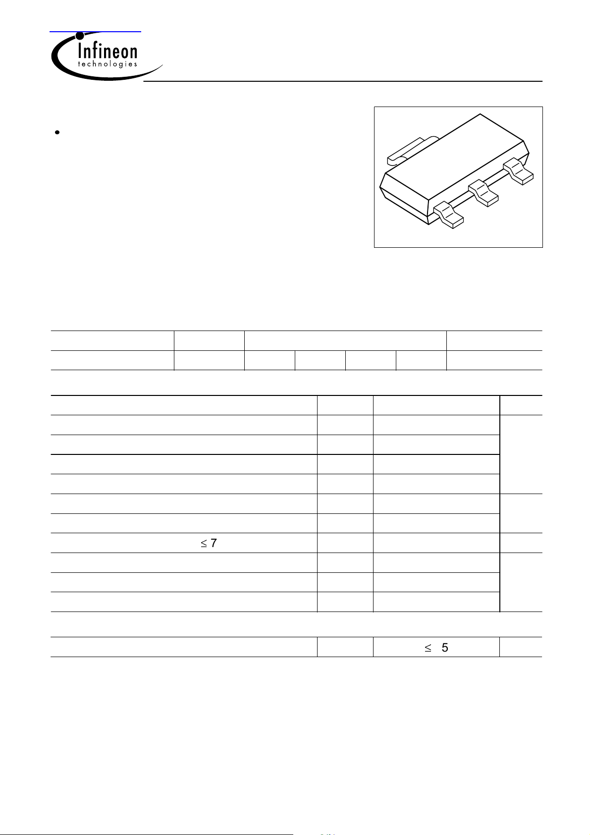
Type Marking Pin Configuration Package
BFG 19S BFG19S 1 = E 2 = B 3 = E 4 = C SOT-223
Maximum Ratings
Parameter
Collector-emitter voltage V
Collector-emitter voltage V
Collector-base voltage V
Symbol Value Unit
CEO
CES
CBO
15 V
20
20
3
2
VPS05163
Emitter-base voltage V
Collector current I
Base current I
Total power dissipation, TS 75 °C
1)
Junction temperature T
Ambient temperature T
Storage temperature T
Thermal Resistance
Junction - soldering point
1
T
is measured on the collector lead at the soldering point to the pcb
S
C
B
P
R
EBO
tot
j
A
stg
thJS
3
100 mA
12
1 W
150 °C
-65 ... 150
-65 ... 150
75
K/W
Oct-26-19991

Electrical Characteristics at TA = 25°C, unless otherwise specified.
BFG 19S
Parameter
DC characteristics
Collector-emitter breakdown voltage
= 1 mA, IB = 0
I
C
Collector-emitter cutoff current
V
= 20 V, VBE = 0
CE
Collector-base cutoff current
V
= 10 V, IE = 0
CB
Emitter-base cutoff current
= 2 V, IC = 0
V
EB
DC current gain
= 70 mA, VCE = 8 V
I
C
Symbol Values Unit
min. typ. max.
V
(BR)CEO
I
CES
I
CBO
I
EBO
h
FE
15 - - V
- - 100 µA
- - 100 nA
- - 10 µA
40 100 220 -
Oct-26-19992
 Loading...