

g
查询BCV29供应商
NPN Silicon Darlington Transistors
BCV29, BCV49
For general AF applications
2
1
High collector current
High current gain
Complementary types: BCV28, BCV48 (PNP)
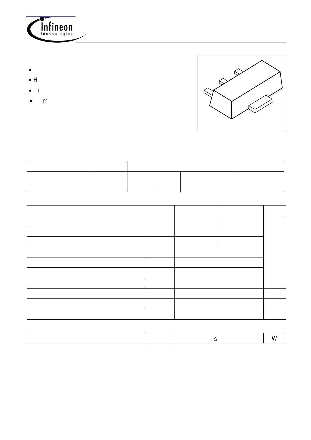
Type Marking Pin Configuration Package
BCV29
BCV49
EF
EG
1 = B
1 = B
2 = C
2 = C
3 = E
3 = E
Maximum Ratings
Parameter
Symbol
3
4 = C
4 = C
BCV29 BCV49
SOT89
SOT89
2
VPS05162
Unit
Collector-emitter voltage
Collector-base voltage
Emitter-base voltage
DC collector current
Peak collector current
Base current 100
Peak base current
Total power dissipation, TS = 130 °C P
Junction temperature
Storage temperature
V
V
V
I
C
I
CM
I
B
I
BM
T
T
CEO
CBO
EBO
tot
j
st
30 60 V
40 80
10 10
500 mA
800
200
1 W
150 °C
-65 ... 150
Thermal Resistance
Junction - soldering point
1
For calculation of R
thJA
1)
please refer to Application Note Thermal Resistance
R
thJS
20 K/W
1 Jul-12-2001

Electrical Characteristics at TA = 25°C, unless otherwise specified.
BCV29, BCV49
Parameter
DC Characteristics
Collector-emitter breakdown voltage
= 10 mA, IB = 0
I
C
Collector-base breakdown voltage
= 100 µA, IB = 0
I
C
Emitter-base breakdown voltage
= 10 µA, IC = 0
I
E
Collector cutoff current
= 30 V, IE = 0
V
CB
= 60 V, IE = 0
V
CB
Collector cutoff current
= 30 V, IE = 0 , TA = 150 °C
V
CB
= 60 V, IE = 0 , TA = 150 °C
V
CB
BCV29
BCV49
BCV29
BCV49
BCV29
BCV49
BCV29
BCV49
Symbol Values Unit
min. typ. max.
V
(BR)CEO
V
(BR)CBO
V
(BR)EBO
I
CBO
I
CBO
30
60
40
80
10 - -
-
-
-
-
-
-
-
-
-
-
-
-
-
-
-
-
100
100
10
10
V
nA
µA
Emitter cutoff current
= 4 V, IC = 0
V
EB
DC current gain 1)
= 100 µA, VCE = 1 V
I
C
DC current gain 1)
= 10 mA, VCE = 5 V
I
C
DC current gain 1)
= 100 mA, VCE = 5 V
I
C
DC current gain 1)
= 0.5 A, VCE = 5 V
I
C
BCV29
BCV49
BCV29
BCV49
BCV29
BCV49
BCV29
BCV49
I
EBO
h
FE
h
FE
h
FE
h
FE
- - 100 nA
4000
2000
10000
4000
20000
10000
4000
2000
-
-
-
-
-
-
-
-
-
-
-
-
-
-
-
-
-
1) Pulse test: t ≤ 300µs, D = 2%
2 Jul-12-2001

Electrical Characteristics at TA = 25°C, unless otherwise specified.
BCV29, BCV49
Parameter
DC Characteristics
Collector-emitter saturation voltage1)
I
= 100 mA, IB = 0.1 mA
C
Base-emitter saturation voltage 1)
I
= 100 mA, IB = 0.1 mA
C
AC Characteristics
Transition frequency
= 50 mA, VCE = 5 V, f = 100 MHz
I
C
Collector-base capacitance
V
= 10 V, f = 1 MHz
CB
Symbol Values Unit
min. typ. max.
V
CEsat
V
BEsat
f
T
C
cb
- - 1 V
- - 1.5
- 150 - MHz
- 3.5 - pF
1) Pulse test: t ≤ 300µs, D = 2%
3 Jul-12-2001

BCV29, BCV49
Total power dissipation P
1200
mW
800
tot
P
600
400
200
0
0 15 30 45 60 75 90 105 120
= f(TS)
tot
°C
T
Collector cutoff current I
= V
V
CB
10
CEmax
4
CBO
= f (TA)
EHP00318BCV 29/49
nA
Ι
CBO
10
10
3
2
max
typ
1
10
0
150
S
10
0
50 100
150
˚C
T
A
Permissible pulse load
P
totmax
P
totmax
totPDC
5
10
5
10
5
10
/ P
2
1
0
-6 -5
10
totDC
10
= f (tp)
D
D
0
0.005
0.01
0.02
0.05
0.1
0.2
0.5
-4
10
=
=
t
T
10
Transition frequency fT = f (IC)
= 5V
V
CE
EHP00319BCV 29/49
t
p
p
T
f
T
10
MHz
10
3
2
5
1
10
-3
10
-2
t
p
0
10s
03
10
10
1
10
EHP00321BCV 29/49
2
Ι
10mA
C
4 Jul-12-2001

BCV29, BCV49
)
Collector-emitter saturation voltage
I
= f (V
C
Ι
C
10
mA
10
10
10
3
2
5
1
5
0
0
), hFE = 1000
CEsat
0.5 1.0
150
25
-50
V
EHP00322BCV 29/49
˚C
˚C
˚C
V
CEsat
1.5
Base-emitter saturation voltage
I
= f (V
C
mA
Ι
C
10
10
10
10
3
2
5
1
5
0
0
), hFE = 1000
BEsat
150
25
-50
1.0 2.0
˚C
˚C
˚C
V
EHP00323BCV 29/49
V
BEsat
3.0
Collector-base capacitance CCB = f (V
Emitter-base capacitance CEB = f (V
10
C
EB0
()
C
CB0
pF
C
CB0
5
C
EB0
0
-1 1
10
10
0
EBO
EHP00324BCV 29/49
V
()
VV
EB0
CBO
10
CB0
DC current gain hFE = f (IC)
)
V
h
CE
FE
= 5V
6
10
5
˚C
10
125
-55
0
25
˚C
˚C
10
1
10
2
5
10
5
4
10
5
3
10
-1 3
10
EHP00325BCV 29/49
10mA
Ι
C
5 Jul-12-2001
 Loading...