

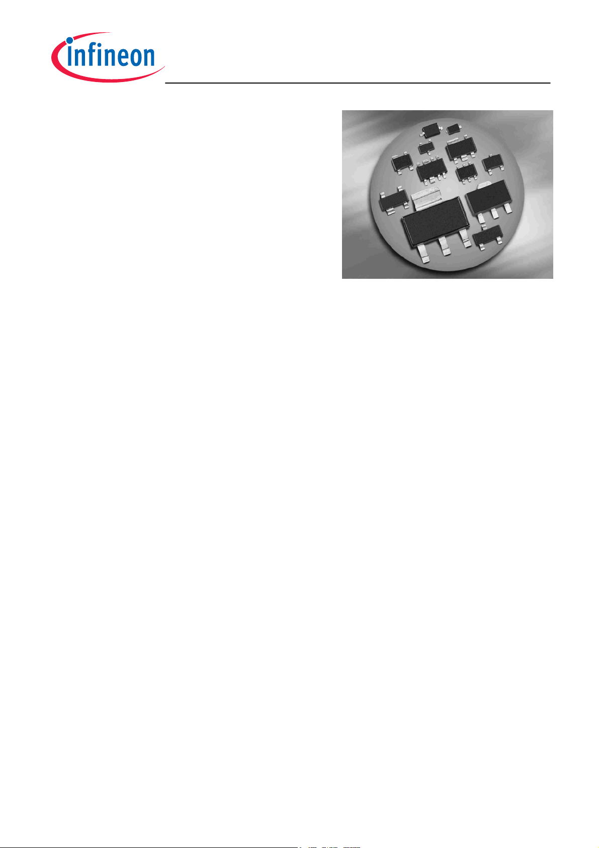
NPN Silicon AF Transistors
• For AF input stages and driver applications
• High current gain
• Low collector-emitter saturation voltage
• Low noise between 30 Hz and 15 kHz
• Complementary types:
BC856...-BC860...(PNP)
BC846...-BC850...
1
2006-09-19
BC846...-BC850...
Type Marking Pin Configuration Package
BC846A
BC846B
BC846BW
BC847A
BC847B
BC847BF
BC847BL3
BC847BT
BC847BW
BC847C
BC847CW
BC848A
BC848AW
BC848B
BC848BF
BC848BL3
1As
1Bs
1Bs
1Es
1Fs
1Fs
1F
1F
1Fs
1Gs
1Gs
1Js
1Js
1Ks
1Ks
1K
1=B
1=B
1=B
1=B
1=B
1=B
1=B
1=B
1=B
1=B
1=B
1=B
1=B
1=B
1=B
1=B
2=E
2=E
2=E
2=E
2=E
2=E
2=E
2=E
2=E
2=E
2=E
2=E
2=E
2=E
2=E
2=E
3=C
3=C
3=C
3=C
3=C
3=C
3=C
3=C
3=C
3=C
3=C
3=C
3=C
3=C
3=C
3=C
-
-
-
-
-
-
-
-
-
-
-
-
-
-
-
-
-
-
-
-
-
-
-
-
-
-
-
-
-
-
-
-
-
-
-
-
-
-
-
-
-
-
-
-
-
-
-
-
SOT23
SOT23
SOT323
SOT23
SOT23
TSFP-3
TSLP-3-1
SC75
SOT323
SOT23
SOT323
SOT23
SOT323
SOT23
TSFP-3
TSLP-3-1
BC848BW
BC848C
BC848CW
BC849B
BC849BF
BC849C
BC849CW
BC850B
BF850BF
BC850BW
BC850C
BC850CW
1Ks
1Ls
1Ls
2Bs
2Bs
2Cs
2Cs
2Fs
2Fs
2Fs
2Gs
2Gs
1=B
1=B
1=B
1=B
1=B
1=B
1=B
1=B
1=B
1=B
1=B
1=B
2=E
2=E
2=E
2=E
2=E
2=E
2=E
2=E
2=E
2=E
2=E
2=E
3=C
3=C
3=C
3=C
3=C
3=C
3=C
3=C
3=C
3=C
3=C
3=C
-
-
-
-
-
-
-
-
-
-
-
-
-
-
-
-
-
-
-
-
-
-
-
-
-
-
-
-
-
-
-
-
-
-
-
-
SOT323
SOT23
SOT323
SOT23
TSFP-3
SOT23
SOT323
SOT23
TSFP-3
SOT323
SOT23
SOT323
2
2006-09-19

Maximum Ratings
BC846...-BC850...
Parameter
Collector-emitter voltage
BC846...
BC847..., BC850...
BC848..., BC849...
Collector-emitter voltage
BC846...
BC847..., BC850...
BC848..., BC849...
Collector-base voltage
BC846...
BC847..., BC850...
BC848..., BC849...
Emitter-base voltage
BC846...
Symbol Value Unit
V
CEO
V
65
45
30
V
CES
80
50
30
V
CBO
80
50
30
V
EBO
6
BC847..., BC850...
BC848..., BC849...
Collector current I
Peak collector current I
Total power dissipation-
T
≤ 71 °C, BC846-BC850
S
T
≤ 128 °C, BC847F-BC850F
S
T
≤ 135 °C, BC847L3-BC848L3
S
T
≤ 109 °C, BC847T
S
T
≤ 124 °C, BC846W-BC850W
S
Junction temperature T
Storage temperature T
C
CM
P
tot
j
stg
6
6
100 mA
200
330
250
250
250
250
150 °C
-65 ... 150
mW
3
2006-09-19

Thermal Resistance
Parameter
BC846...-BC850...
Symbol Value Unit
Junction - soldering point1)
BC846-BC850
BC847F-BC850F
BC847L3-BC848L3
BC847T
BC846W-BC850W
1
For calculation of R
please refer to Application Note Thermal Resistance
thJA
R
thJS
≤ 240
≤ 90
≤ 60
≤ 165
≤ 105
K/W
4
2006-09-19

BC846...-BC850...
Electrical Characteristics at T
= 25°C, unless otherwise specified
Parameter Symbol Values Unit
min. typ. max.
DC Characteristics
Collector-emitter breakdown voltage
I
= 10 mA, IB = 0 , BC846...
C
I
= 10 mA, IB = 0 , BC847..., BC850...
C
I
= 10 mA, IB = 0 , BC848..., BC849...
C
Collector-base breakdown voltage
I
= 10 µA, IE = 0 , BC846...
C
I
= 10 µA, IE = 0 , BC847..., BC850...
C
I
= 10 µA, IE = 0 , BC848..., BC849...
C
Emitter-base breakdown voltage
I
= 0 , IC = 10 µA
E
Collector-base cutoff current
V
= 45 V, IE = 0
CB
V
= 30 V, IE = 0 , TA = 150 °C
CB
V
(BR)CEO
V
(BR)CBO
V
(BR)EBO
I
CBO
65
45
30
80
50
30
-
-
-
-
-
-
- 6 -
-
-
0.015
5
V
-
-
-
-
-
-
µA
-
-
DC current gain1)
I
= 10 µA, VCE = 5 V, hFE-grp.A
C
I
= 10 µA, VCE = 5 V, hFE-grp.B
C
I
= 10 µA, VCE = 5 V, hFE-grp.C
C
I
= 2 mA, VCE = 5 V, hFE-grp.A
C
I
= 2 mA, VCE = 5 V, hFE-grp.B
C
I
= 2 mA, VCE = 5 V, hFE-grp.C
C
Collector-emitter saturation voltage1)
I
= 10 mA, IB = 0.5 mA
C
I
= 100 mA, IB = 5 mA
C
Base emitter saturation voltage1)
I
= 10 mA, IB = 0.5 mA
C
I
= 100 mA, IB = 5 mA
C
Base-emitter voltage1)
I
= 2 mA, VCE = 5 V
C
I
= 10 mA, VCE = 5 V
C
h
FE
V
CEsat
V
BEsat
V
BE(ON)
-
-
-
110
200
420
-
-
-
-
580
-
140
250
480
180
290
520
90
200
700
900
660
-
-
-
-
220
450
800
250
600
-
-
700
770
-
mV
1
Pulse test: t < 300µs; D < 2%
5
2006-09-19

Electrical Characteristics at TA = 25°C, unless otherwise specified
BC846...-BC850...
Parameter
AC Characteristics
Transition frequency
I
= 10 mA, VCE = 5 V, f = 100 MHz
C
Collector-base capacitance
V
= 10 V, f = 1 MHz
CB
Emitter-base capacitance
V
= 0.5 V, f = 1 MHz
EB
Short-circuit input impedance
I
= 2 mA, VCE = 5 V, f = 1 kHz, hFE-grp.A
C
I
= 2 mA, VCE = 5 V, f = 1 kHz, hFE-grp.B
C
I
= 2 mA, VCE = 5 V, f = 1 kHz, hFE-grp.C
C
Open-circuit reverse voltage transf. ratio
I
= 2 mA, VCE = 5 V, f = 1 kHz, hFE-grp.A
C
I
= 2 mA, VCE = 5 V, f = 1 kHz, hFE-grp.B
C
I
= 2 mA, VCE = 5 V, f = 1 kHz, hFE-grp.C
C
Symbol Values Unit
min. typ. max.
f
C
C
h
h
T
cb
eb
11e
12e
- 250 - MHz
- 0.95 - pF
- 9 -
-
-
-
-
-
-
2.7
4.5
8.7
1.5
2
3
kΩ
-
-
-
10
-4
-
-
-
Short-circuit forward current transf. ratio
I
= 2 mA, VCE = 5 V, f = 1 kHz, hFE-grp.A
C
I
= 2 mA, VCE = 5 V, f = 1 kHz, hFE-grp.B
C
I
= 2 mA, VCE = 5 V, f = 1 kHz, hFE-grp.C
C
Open-circuit output admittance
I
= 2 mA, VCE = 5 V, f = 1 kHz, hFE-grp.A
C
I
= 2 mA, VCE = 5 V, f = 1 kHz, hFE-grp.B
C
I
= 2 mA, VCE = 5 V, f = 1 kHz, hFE-grp.C
C
Noise figure
I
= 200 µA, VCE = 5 V, f = 1 kHz,
C
∆ f = 200 Hz, R
= 2 kΩ, BC849..., BC850...
S
Equivalent noise voltage
I
= 200 µA, VCE = 5 V, R
C
= 2 kΩ,
S
f = 10 ... 50 Hz , BC850...
h
h
F
V
21e
22e
n
-
-
-
-
-
-
200
330
600
18
30
60
-
-
-
µS
-
-
-
- 1.2 4 dB
- - 0.135 µV
6
2006-09-19

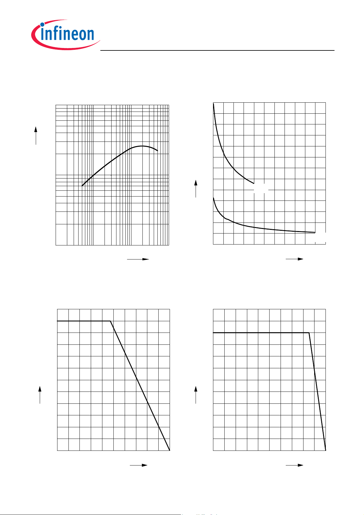
BC846...-BC850...
DC current gain h
V
= 5 V
CE
3
10
5
100
h
FE
2
10
5
1
10
5
0
10
10 10 10 10
C
25
C
-50
C
-2
-1
555
FE
= ƒ(I
0
10
)
C
EHP00365
Collector-emitter saturation voltage
I
= ƒ(V
C
10
2
CEsat
), hFE = 20
EHP00367
mA
Ι
C
100
C
25
C
-50
10
1
C
5
0
10
5
-1
12
mA
Ι
C
10
0
0.1 0.2 0.4
0.3 0.5
V
V
CEsat
Base-emitter saturation voltage
I
= ƒ(V
C
Ι
C
10
10
mA
10
10
2
1
5
0
5
-1
0
), hFE = 20
BEsat
C
100
C
C
25
-50
C
0.2 0.4 0.8
0.6 V 1.2
EHP00364
V
BEsat
Collector cutoff current I
V
= 30 V
CB
4
10
nA
Ι
CB0
3
10
5
2
10
5
1
10
5
0
10
0 50 100 150
CBO
= ƒ(T
max
typ
)
A
EHP00415
˚C
T
A
7
2006-09-19
BC846...-BC850...
Transition frequency f
V
= 5 V
CE
3
10
= ƒ(I
T
MHz
f
T
5
2
10
5
1
10
-1 0 1 2
10 10 10 10
5
5
)
C
EHP00363
mA
Ι
C
Collector-base capacitance C
Emitter-base capacitance C
13
pF
11
10
EB
C
/
9
CB
8
C
7
6
5
4
3
2
1
0
0 4 8 12 16
CEB
eb
= ƒ(V
cb
= ƒ(V
EB
V
VCB/V
CB
)
CCB
)
22
EB
Total power dissipation P
BC846-BC850
360
mW
300
270
240
tot
P
210
180
150
120
90
60
30
0
0 15 30 45 60 75 90 105 120
= ƒ(T
tot
)
S
Total power dissipation P
= ƒ(T
tot
)
S
BC847BF-BC850BF
300
mW
250
225
200
tot
P
175
150
125
100
75
50
25
°C
T
150
S
0
0 15 30 45 60 75 90 105 120
°C
150
T
S
8
2006-09-19

BC846...-BC850...
Total power dissipation P
BC847BL3 / BC848BL3
300
mW
250
225
200
tot
P
175
150
125
100
75
50
25
0
0 15 30 45 60 75 90 105 120
= ƒ(T
tot
)
S
Total power dissipation P
= ƒ(T
tot
)
S
BC847BT
300
mW
250
225
200
tot
P
175
150
125
100
75
50
25
°C
150
T
S
0
0 15 30 45 60 75 90 105 120
°C
150
T
S
Total power dissipation P
BC846W-BC850W
300
mW
250
225
200
tot
P
175
150
125
100
75
50
25
0
0 15 30 45 60 75 90 105 120
= ƒ(T
tot
)
S
Permissible Pulse Load
P
totmax/PtotDC
= ƒ(t
)
p
BC846/W-BC850/W
T
D
0
0.005
0.01
0.02
0.05
0.1
0.2
0.5
-2
EHP00362
=
s
t
p
10
0
3
10
P
totmax
totPDC
10
=
D
2
t
p
t
p
T
5
1
10
5
0
10
°C
150
T
S
-6
10
10-510-410-310
9
2006-09-19

BC846...-BC850...
Permissible Puls Load R
BC847BF-BC850BF
2
10
K/W
1
10
thJS
R
0
10
-1
10
10
-6
10
-5
10
-4
10
thJS
D=0.5
0.2
0.1
0.05
0.02
0.01
0.005
0
-3
= ƒ (t
-2
10
)
p
Permissible Pulse Load
P
totmax/PtotDC
= ƒ(t
)
p
BC847BF-BC850BF
3
10
totDC
/P
2
10
totmax
P
1
10
0
10
s
t
0
10
p
10
-6
10
-5
10
D=0
0.005
0.01
0.02
0.05
0.1
0.2
0.5
-4
10
-3
10
-2
s
t
0
10
p
Permissible Puls Load R
BC847BL3, BC848BL3
2
10
1
10
thJS
R
0
10
-1
10
-7
-6
-5
10
10
10
10
-4
thJS
10
= ƒ (t
0.5
0.2
0.1
0.05
0.02
0.01
0.005
D = 0
-3
10
)
p
Permissible Pulse Load
P
totmax/PtotDC
= ƒ(t
)
p
BC847BL3, BC848BL3
3
10
totDC
/ P
2
10
totmax
P
1
10
0
-2
s
t
0
10
p
10
10
-7
-6
10
-5
10
10
D = 0
0.005
0.01
0.02
0.05
0.1
0.2
0.5
-4
-3
10
10
-2
t
0
s
10
p
10
2006-09-19

BC846...-BC850...
Permissible Puls Load R
BC847BT
3
10
K/W
2
10
thJS
R
1
10
D=0.5
0.2
0.1
0.05
10
0.02
0.01
0.005
0
-4
10
10
10
0
-1
10
-6
10
-5
thJS
-3
= ƒ (t
-2
10
)
p
Permissible Pulse Load
P
totmax/PtotDC
= ƒ(t
)
p
BC847BT
3
10
totDC
/ P
10
D=0
0.005
0.01
0.02
0.05
0.1
0.2
0.5
-4
10
-3
10
-2
s
t
0
10
p
2
10
totmax
P
1
10
0
s
t
0
10
p
10
10
-6
10
-5
Noise figure F = ƒ(V
I
= 0.2mA, R
C
BC 846...850 EHP00370
20
dB
F
15
10
5
0
-1 0 1 2
10 10 10 10
= 2kΩ , f = 1kHz
S
5
CE
)
Noise figure F = ƒ(f)
I
= 0.2 mA, VCE = 5V, R
C
BC 846...850 EHP00371
20
= 2 kΩ
S
dB
F
15
10
5
0
V
V
CE
-2 -1 1 2
10 10 10 10
10
0
kHz
f
11
2006-09-19

BC846...-BC850...
Noise figure F = ƒ(I
V
= 5V, f = 120Hz
CE
BC 846...850 EHP00372
20
dB
F
15
R
= 1 M 100 k 10 k
S
10
5
0
-3 -2 0 1
10 10 10 10
ΩΩΩ
)
C
Ω
500
Ω
1 k
-1
10
mA
Ι
C
Noise figure F = ƒ(I
V
= 5V, f = 1kHz
CE
BC 846...850 EHP00373
20
dB
F
15
R
= 1 M
S
10
Ω
1 k
5
0
-3 -2 0 1
10 10 10 10
)
C
100 k
ΩΩΩ
-1
10
10 k
500
mA
Ι
C
Ω
Noise figure F = ƒ(I
V
= 5V, f = 10kHz
CE
BC 846...850 EHP00374
20
dB
F
15
10
5
0
10 10 10 10
500
Ω
Ω
1 k
-3 -2 0 1
R
)
C
= 1 M
S
10
Ω
-1
100 k
10 k
mA
Ι
C
Ω
Ω
12
2006-09-19

Package Outline
Foot Print
Package SC75
±0.2
1.6
+0.1
0.2
-0.05
A
0.2
0.10
+0.1
-0.05
0.5
M
3
1 2
0.5
0.4
0.1 MAX.
±0.2
1.6
MAX.
10˚
0.2MA
0.7
0.15
±0.1
±0.05
BC846...-BC850...
±0.1
0.8
MAX.
10˚
Marking Layout (Example)
Standard Packing
Reel ø180 mm = 3.000 Pieces/Reel
Reel ø330 mm = 10.000 Pieces/Reel
Pin 1
4
0.65
0.65
0.45
1.15
0.4
0.50.5
2005, December
Date code
BCR108T
Type code
0.2 MAX.
Pin 1
1.75
1.4
13
8
1.8
0.9
2006-09-19

BC846...-BC850...
Date Code marking for discrete packages with
one digit (SCD80, SC79, SC75
Month 2003 2004 2005 2006 2007 2008 2009 2010 2011 2012 2013 2014
01apAPapAPapAP
02bqBQbqBQbqBQ
03crCRcrCRcrCR
04dsDSd sDSd sDS
05et ETet ETe t ET
06fuFUfuFUfuFU
07gvGVgvGVgvGV
08hxHXh xHXhxHX
09jyJYjyJYjyJY
10kzKZk zKZkzKZ
11l2L4l 2L4 l 2L4
12n3N5n3N5n3N5
1)
) CES-Code
1) New Marking Layout for SC75, implemented at October 2005.
.
14
2006-09-19

Package Outline
Foot Print
Package SOT23
±0.1
2.9
12
1)
+0.1
0.4
-0.05
1.9
0.25MBC
1) Lead width can be 0.6 max. in dambar area
B
3
C
0.95
0.8
0.15 MIN.
±0.15
2.4
0.2
±0.1
1
0.1 MAX.
10˚ MAX.
0.08...0.15
0...8˚
M
A
BC846...-BC850...
±0.1
1.3
10˚ MAX.
A
Marking Layout (Example)
Standard Packing
Reel ø180 mm = 3.000 Pieces/Reel
Reel ø330 mm = 10.000 Pieces/Reel
Pin 1
0.8 1.2
EH
4
0.9
s
0.9 0.91.3
Manufacturer
2005, June
Date code (YM)
BCW66
Type code
0.2
Pin 1
3.15
2.13
15
2.65
8
1.15
2006-09-19

Package Outline
Package SOT323
±0.2
2
0.3
+0.1
-0.05
3x
M
0.1
3
0.1 MAX.
0.1
0.9
BC846...-BC850...
±0.1
A
Foot Print
Marking Layout (Example)
12
0.650.65
0.6
0.8
0.65
0.65
1.6
±0.1
2.1
0.1 MIN.
M
0.2 A
0.15
+0.1
-0.05
±0.1
1.25
Standard Packing
Reel ø180 mm = 3.000 Pieces/Reel
Reel ø330 mm = 10.000 Pieces/Reel
Pin 1
Pin 1
4
2.15
Manufacturer
2005, June
Date code (YM)
BCR108W
Type code
0.2
8
2.3
1.1
16
2006-09-19

Package Outline
Foot Print
Package TSFP-3
±0.05
1.2
±0.05
0.2
3
±0.05
±0.05
1.2
12
0.4
0.2
0.4
±0.05
±0.05
±0.05
0.4
0.2
0.55
±0.04
0.15
BC846...-BC850...
±0.05
0.8
10˚ MAX.
±0.05
Marking Layout (Example)
Standard Packing
Reel ø180 mm = 3.000 Pieces/Reel
Reel ø330 mm = 10.000 Pieces/Reel
Pin 1
0.45
1.05
0.4 0.4
Manufacturer
BCR847BF
Type code
Pin 1
4
1.35
0.3
1.2
1.5
17
0.2
8
0.7
2006-09-19

Package TSLP-3-1
Package Outline
Top view Bottom view
+0.1
0.4
0.05 MAX.
1
3
2
Pin 1
marking
1) Dimension applies to plated terminal
0.5
2x0.15
±0.035
0.35
±0.035
±0.05
0.65
±0.05
±0.05
0.6
1)
3
2
1)
Foot Print
For board assembly information please refer to Infineon website "Packages"
1
0.225
0.15
0.6
0.35
0.3
0.35
0.225
0.45
0.945
0.2
0.2
0.17
1)
1
1)
±0.035
0.25
2x
0.275
0.355
R0.1
BC846...-BC850...
±0.035
0.25
±0.05
1
0.315
Marking Layout (Example)
Standard Packing
Reel ø180 mm = 15.000 Pieces/Reel
Stencil aperturesCopper Solder mask
BFR193L3
Type code
Pin 1 marking
Laser marking
4
1.16
8
0.5
Pin 1
marking
0.76
18
2006-09-19

BC846...-BC850...
Edition 2006-02-01
Published by
Infineon Technologies AG
81726 München, Germany
© Infineon Technologies AG 2006.
All Rights Reserved.
Attention please!
The information given in this dokument shall in no event be regarded as a guarantee
of conditions or characteristics (“Beschaffenheitsgarantie”). With respect to any
examples or hints given herein, any typical values stated herein and/or any information
regarding the application of the device, Infineon Technologies hereby disclaims any
and all warranties and liabilities of any kind, including without limitation warranties of
non-infringement of intellectual property rights of any third party.
Information
For further information on technology, delivery terms and conditions and prices
please contact your nearest Infineon Technologies Office ( www.infineon.com).
Warnings
Due to technical requirements components may contain dangerous substances.
For information on the types in question please contact your nearest
Infineon Technologies Office.
Infineon Technologies Components may only be used in life-support devices or
systems with the express written approval of Infineon Technologies, if a failure of
such components can reasonably be expected to cause the failure of that
life-support device or system, or to affect the safety or effectiveness of that
device or system.
Life support devices or systems are intended to be implanted in the human body,
or to support and/or maintain and sustain and/or protect human life. If they fail,
it is reasonable to assume that the health of the user or other persons
may be endangered.
19
2006-09-19
 Loading...