

Page 1
SPXE-9S-R10
9-Slot PICMG 1.3 PCIe Backplane
User Manual Ver. 1.0
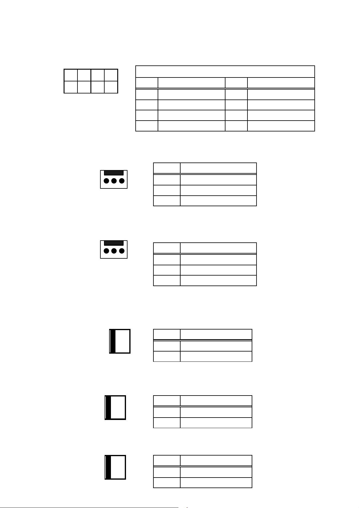
1. J1: PCI-X_A1 Frequency Setting
J2: PCI-X_B1 Frequency Setting
Freq. \ Pin 1 - 2 3 - 4
66MHz Don’t Care Short
100MHz Short Open
133MHz (Default) Open Open
2. J3 & J4: Intel Bridge 41210 SM-BUS Setting
Pin DESCRIPTION
1-2
2-3
Normal Operation
(default)
Test Purposes
Dec. 17, 2007
3. J5: Intel Bridge 41210 Initialization Register Setting
J5 DESCRIPTION
Open (High) Initialization Register
Short (Low)
4. J6: Intel Bridge 41210 Use MCU read/write Pin
Pin DESCRIPTION
1 MCLR
2
3
4
5
Normal response
(default)
+5V
GND
RB7/PGD
RB6/PGC
1
Page 2
5. USB1, USB2: External 4 Port USB Connectors From the Mainboard
7 5 3 1
● ● ● ■
● ● ● ●
USB1、USB2
PIN DESCRIPTION PIN DESCRIPTION
1 USBVCC 2 GND
3 DATA- 4 DATA+
5 DATA+ 6 DATA7 GND 8 USBVCC
6. FAN1, FAN2, FAN3, FAN4: Fan Connector
PIN DESCRIPTION
123
1 GND
2 +12V
3 NC
7. ATXCTL1: Back plane to Mainboard ATX Po wer Co ntrol Connector
123
PIN DESCRIPTION
1 GND
2 PSON#
3 5VSB
8. PWRBTN: External Power On Button
●
■
2
1
PIN DESCRIPTION
1 GND
2 PWRBT#
9. RESET: External Reset Button Connector
●
■
2
1
PIN DESCRIPTION
1 GND
2 SHB_RST#
10. PWRGD: External Power Good Connector
2
●
■
1
PIN DESCRIPTION
1 GND
2 PWRGD
2
Page 3

11. SM-BUS: External System Management BUS Connector
2
1
●
■
PIN DESCRIPTION
1 SMDATA
2 SMBCLK
12.CN2: PCIE X8 SDVO Control Signal Pin
The CN2 indicators are for controlling your PCI E X8 board.
1 2 3
■ ● ●
PIN DESCRIPTION
1 EXP_EN
2 SDVO_CLK
3 SDVO_DAT
13. IOPWR: The I/O Power Connector indicators for controlling your
CPU board.
PIN NO. DESCRIPTION PIN NO. DESCRIPTION
1 GND 2 -12V
3 +12V 4 GND
5 IPMB_DA 6 5VSB
7 GND 8 GND
9 IPMB_CL 10 5VSB
11 +5V 12 PWRGD
13 SMDAT 14 SHB_RST#
15 5VSB 16 GND
17 SMCLK 18 PSON#
19 +3.3V 20 PWRBT#
19 17 15 13 11 9 7 5 3 1
● ● ● ● ● ● ● ● ● ■
● ● ● ● ● ● ● ● ● ●
20 18 16 14 12 10
8642
3
Page 4

14. PCI routing table:
15. Notice:
a. Recommend to use 6mm width spacer to install
b. Torsion must less than 6lb-inch
4
Page 5

16. Dimension:
5
 Loading...