

Page 1
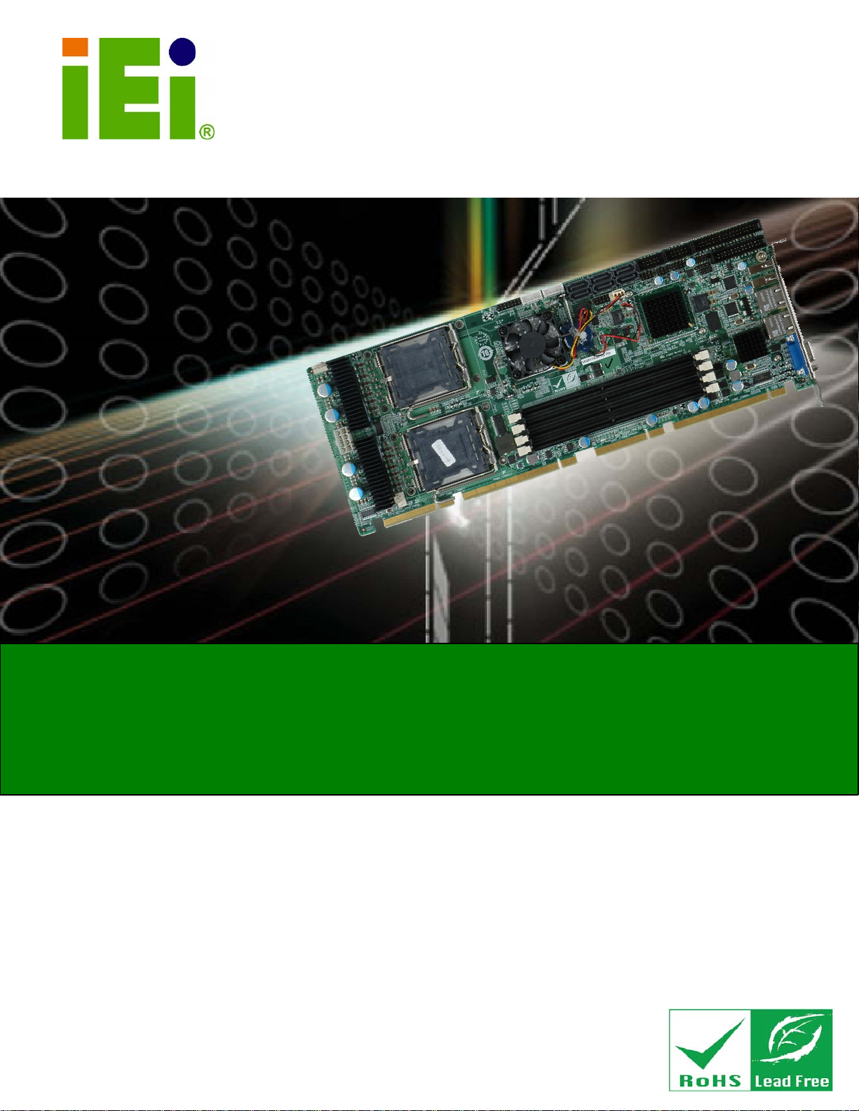
SPCIE-5100DX PICMG 1.3 CPU Card
SPCIE-5100DX PICMG 1.3 CPU Card
IEI Technology Corp.
MODEL:
SPCIE-5100DX
Full-size PICMG 1.3 CPU Card supports Dual LGA771
Intel® Xeon® Processor and comes with VGA, USB,
Dual PCIe GbE, Audio and SATA II with RAID Function
User Manual
Rev. 1.02 – 24 June, 2010
Page i
Page 2

SPCIE-5100DX PICMG 1.3 CPU Card
Revision
Date Version Changes
24 June, 2010 1.02 Added ATX 12 V power cable in the packing list
20 October, 2009 1.01 Added CPU support list (Section 4.4.1) and modified
4.4.3 Cooling Kit Installation
13 July, 2009 1.00 Initial release
Page ii
Page 3
SPCIE-5100DX PICMG 1.3 CPU Card
COPYRIGHT NOTICE
The information in this document is subject to change without prior notice in order to
improve reliability, design and function and does not represent a commitment on the part
of the manufacturer.
In no event will the manufacturer be liable for direct, indirect, special, incidental, or
consequential damages arising out of the use or inability to use the product or
documentation, even if advised of the possibility of such damages.
Copyright
This document contains proprietary information protected by copyright. All rights are
reserved. No part of this manual may be reproduced by any mechanical, electronic, or
other means in any form without prior written permission of the manufacturer.
TRADEMARKS
All registered trademarks and product names mentioned herein are used for identification
purposes only and may be trademarks and/or registered trademarks of their respective
owners.
Page iii
Page 4

SPCIE-5100DX PICMG 1.3 CPU Card
Table of Contents
1 INTRODUCTION..................................................................................................... 1
1.1 OVERVIEW.................................................................................................................. 2
1.1.1 SPCIE-5100DX Expansion Options .................................................................. 2
1.1.1.1 PCI Expansion ............................................................................................ 3
1.1.1.2 USB 2.0 Expansion..................................................................................... 3
1.2 SPCIE-5100DX FEATURES........................................................................................ 3
1.3 SPCIE-5100DX CONNECTOR .................................................................................... 4
1.4 DIMENSIONS............................................................................................................... 5
1.4.1 External Interface Panel Dimensions................................................................ 6
1.5 DATA FLOW................................................................................................................ 7
1.6 TECHNICAL SPECIFICATIONS ...................................................................................... 8
1.7 EXPANSION OPTIONS................................................................................................ 10
1.7.1 Expansion Options Overview........................................................................... 10
1.7.2 IEI Expansion PICMG 1.3 Backplanes ........................................................... 10
1.7.2.1 Limitations.................................................................................................11
1.7.3 IEI Chassis....................................................................................................... 12
2 UNPACKING.......................................................................................................... 13
2.1 ANTI-STATIC PRECAUTIONS...................................................................................... 14
2.2 UNPACKING PRECAUTIONS....................................................................................... 14
2.3 PACKING LIST........................................................................................................... 15
2.3.1 Optional Items.................................................................................................. 16
3 CONNECTOR PINOUTS...................................................................................... 18
3.1 PERIPHERAL INTERFACE CONNECTORS..................................................................... 19
3.1.1 SPCIE-5100DX Layout.................................................................................... 19
3.1.2 Peripheral Interface Connectors ..................................................................... 19
3.1.3 External Interface Panel Connectors............................................................... 20
3.2 INTERNAL PERIPHERAL CONNECTORS ...................................................................... 21
3.2.1 Audio Connector .............................................................................................. 21
3.2.2 Cooling Fan Connectors ( CPU)..................................................................... 22
Page iv
Page 5

SPCIE-5100DX PICMG 1.3 CPU Card
3.2.3 Cooling Fan Connector (Northbridge)............................................................ 23
3.2.4 CPU 12V Power Connector............................................................................. 24
3.2.5 Digital Input/Output (DIO) Connector............................................................ 24
3.2.6 Floppy Disk Connector (34-pin)...................................................................... 25
3.2.7 Front Panel Connector (14-pin)...................................................................... 27
3.2.8 Infrared Interface Connector (5-pin)............................................................... 28
3.2.9 Keyboard Connector........................................................................................ 29
3.2.10 Mouse Connector........................................................................................... 30
3.2.11 Parallel Port Connector................................................................................. 31
3.2.12 SATA Drive Connectors................................................................................. 32
3.2.13 Serial Port Connector (COM1, COM 2)........................................................ 33
3.2.14 SPI Flash Connector...................................................................................... 34
3.2.15 USB Connectors (Internal)............................................................................ 34
3.3 EXTERNAL PERIPHERAL INTERFACE CONNECTOR PANEL ......................................... 35
3.3.1 LAN Connectors............................................................................................... 36
3.3.2 USB Connector ................................................................................................ 37
3.3.3 VGA Connector................................................................................................ 38
4 INSTALLATION .................................................................................................... 39
4.1 ANTI-STATIC PRECAUTIONS...................................................................................... 40
4.2 INSTALLATION CONSIDERATIONS.............................................................................. 41
4.3 INSTALLATION CONSIDERATIONS.............................................................................. 42
4.4 CPU, CPU COOLING KIT AND DIMM INSTALLATION.............................................. 43
4.4.1 CPU Support List............................................................................................. 43
4.4.2 Socket LGA771 CPU Installation.................................................................... 45
4.4.3 Cooling Kit Installation ................................................................................... 48
4.4.4 DIMM Installation........................................................................................... 51
4.5 JUMPER SETTINGS .................................................................................................... 53
4.5.1 Clear CMOS Jumper........................................................................................ 53
4.6 CHASSIS INSTALLATION............................................................................................ 55
4.6.1 Airflow.............................................................................................................. 55
4.6.2 Backplane Installation..................................................................................... 55
4.6.3 CPU Card Installation..................................................................................... 56
4.7 INTERNAL PERIPHERAL DEVICE CONNECTIONS........................................................ 56
4.7.1 Audio Kit Installation (Optional)..................................................................... 56
Page v
Page 6

4.7.2 FDD Cable Connection (Optional) ................................................................. 57
4.7.3 Keyboard and Mouse PS/2 Cable with Bracket (Optional)............................. 58
4.7.4 Dual RS-232 Cable Connection....................................................................... 60
4.7.5 Parallel Port Cable with Slot Bracket (Optional) ........................................... 61
4.7.6 SATA Drive Connection................................................................................... 63
4.7.7 USB Cable (Dual Port).................................................................................... 65
4.8 EXTERNAL PERIPHERAL INTERFACE CONNECTION................................................... 66
4.8.1 LAN Connection (Single Connector)............................................................... 66
4.8.2 USB Device Connection (Single Connector)................................................... 67
4.8.3 VGA Monitor Connection ................................................................................ 68
4.9 CONNECTING THE SPCIE-5100DX TO THE BACKPLANE.......................................... 69
5 BIOS SCREENS...................................................................................................... 71
5.1 INTRODUCTION......................................................................................................... 72
5.1.1 Starting Setup................................................................................................... 72
SPCIE-5100DX PICMG 1.3 CPU Card
5.1.2 Using Setup...................................................................................................... 72
5.1.3 Getting Help..................................................................................................... 73
5.1.4 Unable to Reboot After Configuration Changes.............................................. 73
5.1.5 BIOS Menu Bar................................................................................................ 73
5.2 MAIN........................................................................................................................ 74
5.3 ADVANCED............................................................................................................... 75
5.3.1 CPU Configuration.......................................................................................... 76
5.3.2 IDE Configuration........................................................................................... 77
5.3.2.1 IDE Master, IDE Slave and Serial-ATA Primary/Secondary Channel...... 79
5.3.3 Floppy Configuration....................................................................................... 85
5.3.4 Super IO Configuration ................................................................................... 86
5.3.5 Hardware Health Configuration...................................................................... 89
5.3.6 AHCI Configuration......................................................................................... 93
5.3.6.1 AHCI Port n.............................................................................................. 94
5.3.7 Remote Access Configuration.......................................................................... 96
5.3.8 USB Configuration........................................................................................... 99
5.4 PCI/PNP................................................................................................................. 100
5.5 BOOT...................................................................................................................... 103
5.5.1 Boot Settings Configuration........................................................................... 103
5.5.2 Boot Device Priority...................................................................................... 106
Page vi
Page 7

SPCIE-5100DX PICMG 1.3 CPU Card
5.5.3 Removable Drives.......................................................................................... 106
5.6 SECURITY............................................................................................................... 108
5.7 CHIPSET ................................................................................................................. 109
5.7.1 South Bridge Configuration............................................................................110
5.8 EXIT........................................................................................................................112
6 RAID SETUP .........................................................................................................114
6.1 INTRODUCTION........................................................................................................115
6.1.1 Precautions.....................................................................................................115
6.2 FEA TURES AND BENEFITS........................................................................................116
6.3 ACCESSING THE INTEL
®
MATRIX STORAGE MANAGER............................................116
6.4 INST ALLING THE OPERATING SYSTEM TO THE RAID ARRAY ...................................117
6.5 RAID CONFIGURATION ...........................................................................................118
6.5.1 Creating a RAID Volume.................................................................................118
6.5.2 Deleting a RAID Volume................................................................................ 122
6.5.3 Resetting a Disk to Non-RAID....................................................................... 125
6.5.4 Exiting the Matrix Storage Manager............................................................. 127
7 SOFTWARE DRIVERS....................................................................................... 129
7.1 AVAILABLE SOFTWARE DRIVERS............................................................................ 130
7.2 DRIVER CD AUTO-RUN.......................................................................................... 130
7.3 CHIPSET DRIVER INSTALLATION............................................................................. 132
7.4 XGI VGA DRIVER INSTALLATION.......................................................................... 136
7.5 INTEL® GBE LAN DRIVER.................................................................................... 138
7.6 HD AUDIO KIT DRIVER INSTALLATION.................................................................. 141
7.6.1 BIOS Setup..................................................................................................... 141
7.6.2 Driver Installation ......................................................................................... 141
7.7 INTEL
®
MATRIX STORAGE MANAGER DRIVER INSTALLATION................................ 144
A BIOS OPTIONS.................................................................................................... 149
B TERMINOLOGY................................................................................................. 153
C WATCHDOG TIME R.......................................................................................... 157
D HAZARDOUS MATERIALS DISCLOSURE................................................... 160
D.1 HAZARDOUS MATERIAL DISCLOSURE TABLE FOR IPB PRODUCTS CERTIFIED AS
ROHS COMPLIANT UNDER 2002/95/EC WITHOUT MERCURY ..................................... 161
Page vii
Page 8

E RAID LEVELS...................................................................................................... 164
E.1 INTRODUCTION ...................................................................................................... 165
E.1.1 RAID 0 or Disk Striping................................................................................ 165
E.1.2 RAID 1 or Disk Mirroring............................................................................. 165
E.1.3 RAID 10 or Disk Mirroring and Striping ...................................................... 165
E.1.4 RAID 5........................................................................................................... 166
SPCIE-5100DX PICMG 1.3 CPU Card
Page viii
Page 9
SPCIE-5100DX PICMG 1.3 CPU Card
List of Figures
Figure 1-1: SPCIE-5100DX PICMG 1.3 CPU Card.......................................................................2
Figure 1-2: SPCIE-5100DX Overview [Front View].....................................................................4
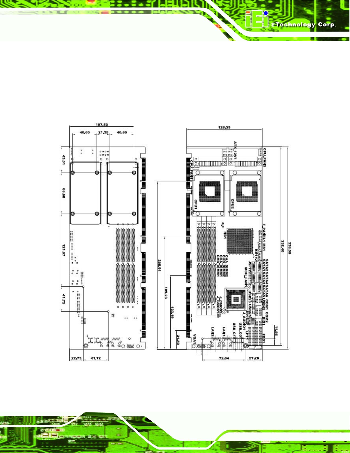
Figure 1-3: SPCIE-5100DX Dimensions (mm).............................................................................5
Figure 1-4: External Interface Panel Dimensions (mm).............................................................6
Figure 1-5: Data Flow Block Diagram..........................................................................................7
Figure 3-1: Connector and Jumper Locations..........................................................................19
Figure 3-2: Audio Connector Location (9-pin)..........................................................................21
Figure 3-3: +12V Fan Connector Location................................................................................22
Figure 3-4: +12V Fan Connector Location................................................................................23
Figure 3-5: CPU 12V Power Connector Location.....................................................................24
Figure 3-6: DIO Connector Location..........................................................................................25
Figure 3-7: 34-pin FDD Connector Location.............................................................................26
Figure 3-8: Front Panel Connector Pinout Locations (14-pin)................................................27
Figure 3-9: Infrared Connector Pinout Locations ....................................................................28
Figure 3-10: Keyboard Connector Location .............................................................................29
Figure 3-11: Mouse Connector Location...................................................................................30
Figure 3-12: Parallel Port Connector Location.........................................................................31
Figure 3-13: SATA Drive Connector Locations........................................................................32
Figure 3-14: Serial Connector Pinout Locations......................................................................33
Figure 3-15: SPI Flash Connector Pinouts................................................................................34
Figure 3-16: USB Connector Pinout Locations........................................................................35
Figure 3-17: SPCIE-5100DX External Peripheral Interface Connector...................................36
Figure 3-18: RJ-45 Ethernet Connector.....................................................................................37
Figure 3-19: VGA Connector ......................................................................................................38
Figure 4-1: Intel LGA771 Socket ................................................................................................45
Figure 4-2: Remove Protective Cover .......................................................................................46
Figure 4-3: CPU Socket Load Plate ...........................................................................................46
Figure 4-4: Insert the Socket LGA771 CPU...............................................................................47
Page ix
Page 10

Figure 4-5: CPU 12V Power Connector .....................................................................................48
Figure 4-6: IEI LGA771 Cooling Kit............................................................................................48
Figure 4-7: CPU Fan Installation – Retention Screws Removal..............................................49
Figure 4-8: CPU Fan Installation – First....................................................................................50
Figure 4-9: CPU Fan Installation – Second...............................................................................50
Figure 4-10: Installing a DIMM....................................................................................................52
Figure 4-11: Clear CMOS Jumper ..............................................................................................54
Figure 4-12: Audio Kit Connection ............................................................................................57
Figure 4-13: FDD Cable Connection..........................................................................................58
Figure 4-14: Keyboard and Mouse PS/2 Cable with Bracket ..................................................59
Figure 4-15: PS/2 Connector ......................................................................................................60
Figure 4-16: Dual RS-232 Cable Installation.............................................................................61
Figure 4-17: LPT Cable Connection...........................................................................................62
SPCIE-5100DX PICMG 1.3 CPU Card
Figure 4-18: Connect the LPT Device........................................................................................63
Figure 4-19: SATA Drive Cable Connection..............................................................................64
Figure 4-20: SATA Power Drive Connection.............................................................................64
Figure 4-21: Dual USB Cable Connection.................................................................................65
Figure 4-22: LAN Connection.....................................................................................................67
Figure 4-23: USB Device Connection........................................................................................68
Figure 4-24: VGA Connector ......................................................................................................69
Figure 4-25: SPCIE-5100DX Installation....................................................................................70
Figure 7-1: Introduction Screen.............................................................................................. 131
Figure 7-2: OS Selection Screen............................................................................................. 131
Figure 7-3: Available Drivers................................................................................................... 132
Figure 7-4: Chipset Driver Welcome Screen.......................................................................... 133
Figure 7-5: Chipset Driver License Agreement..................................................................... 133
Figure 7-6: Chipset Driver Read Me File ................................................................................ 134
Figure 7-7: Chipset Driver Setup Operations ........................................................................ 135
Figure 7-8: Chipset Driver Installation Finish Screen........................................................... 135
Figure 7-9: Preparing VGA Driver Setup................................................................................ 136
Figure 7-10: VGA Driver Welcome Screen............................................................................. 137
Figure 7-11: Windows Logo Testing....................................................................................... 137
Page x
Page 11

SPCIE-5100DX PICMG 1.3 CPU Card
Figure 7-12: VGA Driver Installation Complete Screen........................................................ 138
Figure 7-13: LAN Driver Welcome Screen ............................................................................. 139
Figure 7-14: LAN Driver License Agreement......................................................................... 139
Figure 7-15: LAN Driver Setup Options.................................................................................. 140
Figure 7-16: LAN Driver Installation Ready Window ............................................................ 140
Figure 7-17: LAN Driver Installation Progress....................................................................... 141
Figure 7-18: Preparing Setup Screen..................................................................................... 142
Figure 7-19: InstallShield Wizard Welcome Screen.............................................................. 142
Figure 7-20: Audio Driver Software Configuration................................................................ 143
Figure 7-21: Restart the Computer......................................................................................... 143
Figure 7-22: SATA RAID Driver Installation Program........................................................... 144
Figure 7-23: InstallShield Wizard Setup Screen.................................................................... 145
Figure 7-24: Matrix Storage Manager Setup Screen............................................................. 145
Figure 7-25: Matrix Storage Manager Welcome Screen....................................................... 146
Figure 7-26: Matrix Storage Manager Warning Screen......................................................... 146
Figure 7-27: Matrix Storage Manager License Agreement................................................... 147
Figure 7-28: Matrix Storage Manager Readme File............................................................... 147
Figure 7-29: Matrix Storage Manager Setup Complete......................................................... 148
Page xi
Page 12
SPCIE-5100DX PICMG 1.3 CPU Card
List of Tables
Table 1-1: Technical Specifications...........................................................................................10
Table 1-2: Compatible IEI PICMG 1.3 Backplanes....................................................................11
Table 1-3: Backplane Limitations ..............................................................................................11
Table 1-4: Compatible IEI Chassis.............................................................................................12
Table 2-1: Package List Contents..............................................................................................16
Table 2-2: Package List Contents..............................................................................................16
Table 3-1: Peripheral Interface Connectors..............................................................................20
Table 3-2: Rear Panel Connectors.............................................................................................20
Table 3-3: Audio Connector Pinouts.........................................................................................21
Table 3-4: CPU Fan Connector Pinouts ....................................................................................22
Table 3-5: Northbridge Fan Connector Pinouts .......................................................................23
Table 3-6: CPU 12V Power Connector Pinouts.........................................................................24
Table 3-7: DIO Connector Pinouts.............................................................................................25
Table 3-8: 34-pin FDD Connector Pinouts ................................................................................26
Table 3-9: Front Panel Connector Pinouts (14-pin) .................................................................28
Table 3-10: Infrared Connector Pinouts....................................................................................29
Table 3-11: Keyboard Connector Pinouts.................................................................................29
Table 3-12: Mouse Connector Pinouts......................................................................................30
Table 3-13: Parallel Port Connector Pinouts ............................................................................31
Table 3-14: SATA Drive Connector Pinouts..............................................................................32
Table 3-15: Serial Connector Pinouts........................................................................................33
Table 3-16: SPI Flash Connector ...............................................................................................34
Table 3-17: USB Port Connector Pinouts..................................................................................35
Table 3-18: LAN Pinouts.............................................................................................................36
Table 3-19: RJ-45 Ethernet Connector LEDs............................................................................37
Table 3-20: USB Port Pinouts.....................................................................................................38
Table 3-21: VGA Connector Pinouts..........................................................................................38
Table 4-1: Intel® Xeon® Processor Support List .....................................................................44
Page xii
Page 13

SPCIE-5100DX PICMG 1.3 CPU Card
Table 4-2: Jumpers......................................................................................................................53
Table 4-3: Clear CMOS Jumper Settings...................................................................................54
Table 5-1: BIOS Navigation Keys...............................................................................................73
Page xiii
Page 14

SPCIE-5100DX PICMG 1.3 CPU Card
BIOS Menus
Menu 1: Main................................................................................................................................74
Menu 2: Advanced.......................................................................................................................76
Menu 3: CPU Configuration........................................................................................................76
Menu 4: IDE Configuration..........................................................................................................77
Menu 5: IDE Master and IDE Slave Configuration....................................................................80
Menu 6: Floppy Configuration....................................................................................................85
Menu 7: Super IO Configuration ................................................................................................86
Menu 8: Hardware Health Configuration...................................................................................89
Menu 9: AHCI Configuration.......................................................................................................94
Menu 10: AHCI Port n Configuration Menu...............................................................................95
Menu 11: Remote Access Configuration [Advanced]..............................................................96
Menu 12: USB Configuration......................................................................................................99
Menu 13: PCI/PnP Configuration ............................................................................................ 101
Menu 14: Boot........................................................................................................................... 103
Menu 15: Boot Settings Configuration................................................................................... 104
Menu 16: Boot Device Priority Settings................................................................................. 106
Menu 17: Removable Drives.................................................................................................... 107
Menu 18: Security..................................................................................................................... 108
Menu 19: Chipset...................................................................................................................... 109
Menu 20:SouthBridge Chipset Configuration ....................................................................... 110
Menu 21:Exit.............................................................................................................................. 112
Page xiv
Page 15
SPCIE-5100DX PICMG 1.3 CPU Card
1 Introduction
Chapter
1
Page 1
Page 16
1.1 Overview
Figure 1-1: SPCIE-5100DX PICMG 1.3 CPU Card
SPCIE-5100DX PICMG 1.3 CPU Card
The SPCIE-5100DX PICMG 1.3 form factor CPU card is an Intel® Xeon®
platform with an integrated Intel® 5100 and ICH9R chipset. The SPCIE-5100DX is
coupled with the specially designed backplanes to provide access to up to 20 PCI Express
(PCIe) lanes.
Four 8.0 GB DDR2 SDRAM Registered ECC DIMMs support a maximum of 32.0 GB
DDR2 system memory. Six SATA II drives with 3.0 Gbps data transmission rates provide
flexible storage options. Twelve USB 2.0 interfaces and four PCI expansion lanes
(interfaced to the backplane) provide further expansion options. Dual PCIe gigabit
Ethernet (GbE) controllers facilitate external Internet connectivity. An XGI Volari™ PCI
graphics controller supports analog CRT display output and connectivity to standard CRT
monitors through an external VGA connector.
CPU processor
1.1.1 SPCIE-5100DX Expansion Options
There are 20 PCIe x1 lanes on the SPCIE-5100DX. All of these, 20 PCIe x1 lanes are
Page 2
interfaced to the IEI SPXE backplane through the PICMG 1.3 form factor edge connectors
(one PCIe x16 and one PCIe x4) on the bottom of the CPU card.
Page 17
SPCIE-5100DX PICMG 1.3 CPU Card
1.1.1.1 PCI Expansion
An additional four PCI lanes are interfaced to the backplane through the standard PCI
edge connectors on the bottom of the SPCIE-5100DX CPU card.
1.1.1.2 USB 2.0 Expansion
Twelve USB 2.0 interfaces are also available. Eight of the USB 2.0 interfaces are
implemented directly on the SBC (six internal and two external) and the remaining four
USB 2.0 interfaces are connected to the backplane through the edge connectors.
1.2 SPCIE-5100DX Features
Some of the SPCIE-5100DX features are listed below.
Supports dual LGA771 Intel® Xeon® processors with a 1066 MHz or
1333 MHz FSB
Supports four 240-pin 8.0 GB (max.) 533 MHz or 667 MHz DDR2 ECC
Registered DIMM (system max. 32.0 GB)
Supports up to 1600 x 1200 resolution VGA output
Six SATA II drives with data transfer rates of 3.0 Gbps supported
Twelve USB 2.0 devices supported (eight on-board and four on the
backplane)
Dual PCIe GbE Ethernet connectors
PICMG 1.3 form factor
RoHS compliant
Supports ATX power supplies
Page 3
Page 18
1.3 SPCIE-5100DX Connector
The SPCIE-5100DX has a wide variety of peripheral interface connectors. Figure 1-2 is a
labeled photo of the peripheral interface connectors on the SPCIE-5100DX.
SPCIE-5100DX PICMG 1.3 CPU Card
Page 4
Figure 1-2: SPCIE-5100DX Overview [Front View]
Page 19
SPCIE-5100DX PICMG 1.3 CPU Card
1.4 Dimensions
The dimensions of the board are listed below:
Length: 338.58 mm
Width: 126.39 mm
Figure 1-3: SPCIE-5100DX Dimensions (mm)
Page 5
Page 20
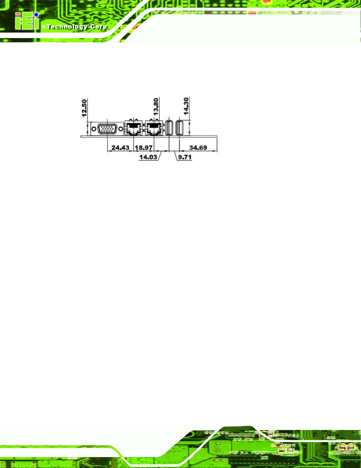
1.4.1 External Interface Panel Dimensions
External peripheral interface connector panel dimensions are shown in Figure 1-4.
Figure 1-4: External Interface Panel Dimensions (mm)
SPCIE-5100DX PICMG 1.3 CPU Card
Page 6
Page 21
SPCIE-5100DX PICMG 1.3 CPU Card
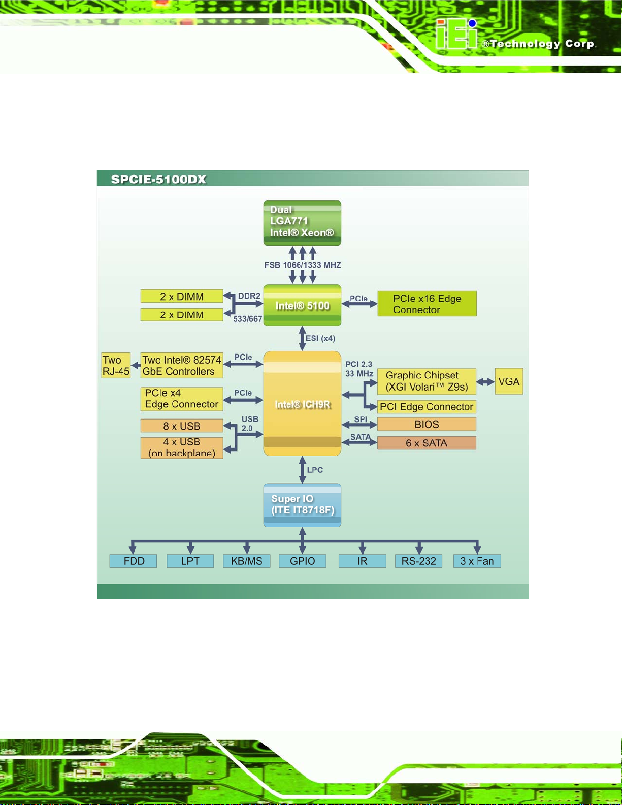
1.5 Data Flow
Figure 1-5 shows the data flow between the two on-board chipsets and other components
installed on the motherboard and described in the following sections of this chapter.
Figure 1-5: Data Flow Block Diagram
Page 7
Page 22
1.6 Technical Specifications
SPCIE-5100DX technical specifications are listed below.
Specification SPCIE-5100DX
SPCIE-5100DX PICMG 1.3 CPU Card
Form Factor
Socket
CPU Supported
Front Side Bus (FSB)
Northbridge Chipset
Southbridge Chipset
Memory
Audio
PICMG 1.3
LGA771 (Socket J)
Intel® dual-core Xeon® 5100 series CPU
Intel® dual-core Xeon® 5200 series CPU
Intel® quad-core Xeon® 5300 series CPU
Intel® quad-core Xeon® 5400 series CPU
1066 MHz or 1333 MHz
Intel® 5100 MCH
Intel® ICH9R
Four 240-pin 8.0 GB (max.) 667 MHz or 533 MHz
dual-channel DDR2 SDRAM ECC Registered DIMM
supported (system max. 32.0 GB)
Optional 7.1 channel HD Audio kit with Realtek ALC883
audio codec
LAN
Super I/O Controller
BIOS
Watchdog Timer
Digital I/O
Expansion
PCI
PCIe
Page 8
Two Intel® 82574L PCIe GbE controllers
ITE IT8718F
AMI SPI BIOS
Software programmable supports 1~2 55 sec. system reset
8-bit digital I/O, 4-bit input and 4-bit output
Four PCI slots
PCIe x16 signal to backplane
PCIe x4 signal to backplane
Page 23
SPCIE-5100DX PICMG 1.3 CPU Card
Specification SPCIE-5100DX
I/O Interface Connectors
Display port
Ethernet
Keyboard/Mouse
LPT
Serial Ports
USB 2.0/1.1 ports
Infrared
Storage
Floppy Disk Drives
One VGA via XGI Volari™ Z9s PCI graphics controller
GPU integrated with 64-bit 64MB GDDR2 memory
Supports resolution up to UXGA(1600x1200) and
CRT hot plug
Two RJ-45 ports
One 5-pin keyboard/mouse pin-header connector
One IEEE 1284 parallel port supporting normal, EPP and
ECP modes
Two RS-232 seri al ports
Twelve USB 2.0 devices supported, eight on-board and
four on the backplane
One infrared connector
One 5.25” 360 KB or 1.2 MB floppy disk drives (FDD) or
3.5” 720 KB, 1.44 MB, 2.88 MB FDD.
Serial ATA
Environmental and Power Specifications
Power Supply
Power Consumption
Operating temperature
Humidity
Six independent serial ATA (SATA) channels with 3.0 Gb/s
data transfer rates support RAID 0, 1, 5 and 10
ATX supported
3.3 V @ 1.07 A
5 V @ 5.55 A
12 V @ 12.3 A
Dual 1.60 GHz 5110 Intel® Xeon® CPUs with 1066 MHz
FSB and four 2.0 GB of 667 MHz DDR2 memory running
with 3D Mark 2001SE
0ºC ~ 60ºC
0% ~ 95% (non-condensing)
Page 9
Page 24
Specification SPCIE-5100DX
Physical Specifications
SPCIE-5100DX PICMG 1.3 CPU Card
Dimensions
Weight GW/NW
338 mm x 126 mm
1200g/950g
Table 1-1: Technical Specifications
1.7 Expansion Options
1.7.1 Expansion Options Overview
A number of compatible IEI Technology Corp. PICMG 1.3 backplanes and chassis can be
used to develop and expanded system. These backplanes and chassi s are listed below.
1.7.2 IEI Expansion PICMG 1.3 Backplanes
The backplanes listed in Table 1-2 are compatible with the SPCIE-5100DX and can be
used to develop highly integrated industrial applications. All of the backplanes listed below
have 24-pin ATX connector and a 4-pin ATX connector. For more information about these
backplanes please consult the IEI catalog or contact your vendor, reseller or the IEI sales
team at
sales@iei.com.tw.
NOTE:
All the PCIe x16 slots in the Table 1-2 only have PCIe x8 signals
transmitted to them and NOT PCIe x16 signals.
Page 10
Page 25
SPCIE-5100DX PICMG 1.3 CPU Card
Expansion Slots
Model Total Slots System
PCIe
System Type
PCI-X PCI
x8 x4 x1
SPE-4S 4 One 2* 1 - - - Single
SPE-6S 6 One - 5* - - - Single
SPE-9S 9 One 2* 3 - - 3 Single
SPXE-9S 9 One 2* 2 - 2 2 Single
SPXE-14S 14 One 1* - 12* - - Single
*There are some limitations for certain expansion slots when the SPCIE-5100DX is
installed on the backplane. Please see the section below (Section
details.
1.7.2.1) for more
Table 1-2: Compatible IEI PICMG 1.3 Backplanes
1.7.2.1 Limitations
The limitations for certain expansions slots on the backplanes when installed with
SPCIE-5100DX are listed below.
Backplanes Slot Label Limitation
SPE-4S
SPE-6S
SPE-9S PCIEX8_1 This PCIe x8 slot is not supported by the SPCIE-5100DX
SPXE-9S PCIEX8_1 This PCIe x8 slot is not supported by the SPCIE-5100DX
SPXE-14S
PCIEX8_1 The length of the expansion card install ed in this
PCIe x8 slot should be less than 21cm.
PCIEX4_1
PCIEX4_2
PCIEX1_A1 This PCIe x1 slot is not supported by the SPCIE-5100DX
PCIEX8_1 The length of the expansion card install ed in this
The length of the expansion card installed in these two
PCIe x4 slots should be less than 21cm.
PCIe x8 slot should be less than 21cm.
Table 1-3: Backplane Limitations
Page 11
Page 26
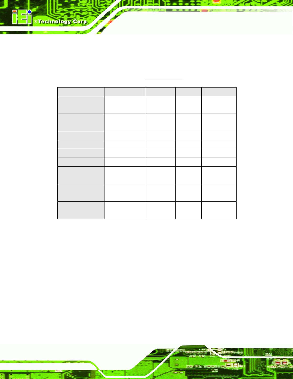
1.7.3 IEI Chassis
IEI chassis available for SPCIE-5100DX system development are listed in Table 1-4. For
more information about these chassis please consult the IEI catalog or contact your
SPCIE-5100DX PICMG 1.3 CPU Card
vendor, reseller or the IEI sales team at
sales@iei.com.tw.
Model Slot SBC Mounting Max Slots Backplanes
PAC-106G-R20 Full-size Wall 6 SPE-4S
SPE-6S
PAC-107G-R20 Full-size Wall 6 SPE-4S
SPE-6S
RACK-305G-R20 Full-size (4U) Rack 14 SPXE-14S
RACK-360G-R20 Full-size (4U) Rack 14 SPXE-14S
RACK-814G-R20 Full-size (4U) Rack 14 SPXE-14S
RACK-3000G-R20 Full-size (4U) Rack 14 SPXE-14S
PAC-125G-R20 Full-size Wall 10 SPE-9S
SPXE-9S
PAC-1000G-R20 Full-size Wall 6 SPE-4S
SPE-6S
PACO-506F Full-size Wall 6 SPE-4S
SPE-6S
Page 12
Table 1-4: Compatible IEI Chassis
Page 27
SPCIE-5100DX PICMG 1.3 CPU Card
Chapter
2
2 Unpacking
Page 13
Page 28
2.1 Anti-static Precautions
WARNING:
Static electricity can destroy certain electronics. Make sure to follow the
ESD precautions to prevent damage to the product, and injury to the
user.
Make sure to adhere to the following guidelines:
Wear an anti-static wristband: - Wearing an anti-static wristband can
prevent electrostatic discharge.
Self-grounding:- Touch a grounded conductor every few minutes to
SPCIE-5100DX PICMG 1.3 CPU Card
discharge any excess static buildup.
Use an anti-static pad: When configuring any circuit board, place it on an
anti-static mat.
Only handle the edges of the PCB:- Don't touch the surface of the
motherboard. Hold the motherboard by the edges when handling.
2.2 Unpacking Precautions
When the SPCIE-5100DX is unpacked, please do the following:
Follow the antistatic guidelines above.
Make sure the packing box is facing upwards whe n opening.
Make sure all the packing list items are present.
Page 14
Page 29
SPCIE-5100DX PICMG 1.3 CPU Card
2.3 Packing List
NOTE:
If any of the components listed in the checklist below are missing, do
not proceed with the installation. Contact the IEI reseller or vendor the
SPCIE-5100DX was purchased from or contact an IEI sales
representative directly by sending an email to
The SPCIE-5100DX is shipped with the following components:
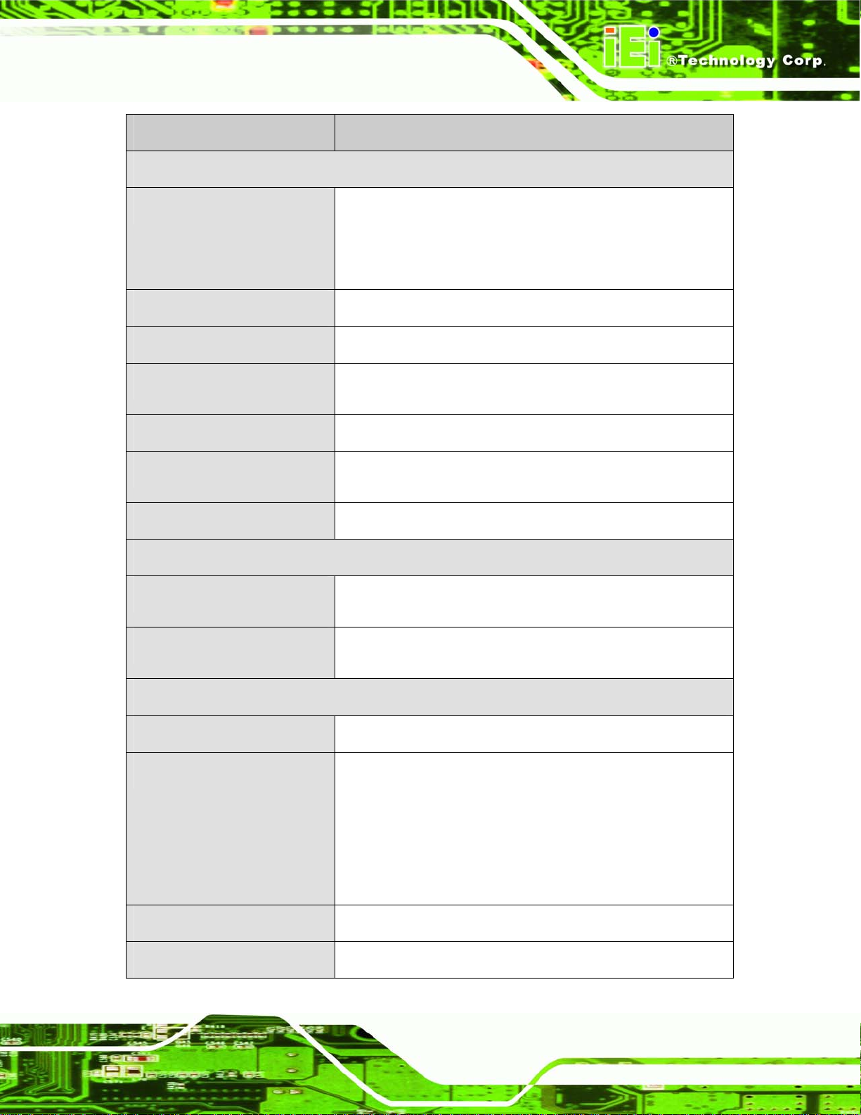
Quantity Item and Part Number Image
1 SPCIE-5100DX
1 Dual RS-232 cable
(P/N: 19800-000051-RS)
6 SATA cables
(P/N: 32000-062800-RS)
32sales@iei.com.tw.
1 Dual USB cable (w bracket)
(P/N: CB-USB02-RS)
1 ATX 12V power cable
(P/N: 32102-008000-100-RS)
Page 15
Page 30
2 LGA771 CPU coolers
(P/N: 19100-000110-RS)
1 Mini jumper Pack
1 Quick Installation Guide
1 Utility CD
SPCIE-5100DX PICMG 1.3 CPU Card
Table 2-1: Package List Contents
2.3.1 Optional Items
Audio kit
(P/N: AC-KIT-833HD-R10)
FDD cable
(P/N: 32200-000017-RS)
Parallel port cable
(P/N:19800-000049-RS)
KB/MS cable
(P/N: 19800-000066-RS)
Page 16
SATA power cables
(P/N: 32100-088600-RS)
Table 2-2: Package List Contents
Page 31

SPCIE-5100DX PICMG 1.3 CPU Card
Page 17
Page 32

SPCIE-5100DX PICMG 1.3 CPU Card
Chapter
3
3 Connector Pinouts
Page 18
Page 33

SPCIE-5100DX PICMG 1.3 CPU Card
3.1 Peripheral Interface Connectors
This chapter details all the jumpers and connectors.
3.1.1 SPCIE-5100DX Layout
The figures below show all the connectors and jumpers.
Figure 3-1: Connector and Jumper Locations
3.1.2 Peripheral Interface Connectors
The table below lists all the connectors on the board.
Connector Type Label
Audio connector 10-pin header J_AUDIO1
Battery connector 2-pin wafer BAT1
Cooling fan connector, CPU 4-pin wafer CPU_FAN1
Cooling fan connector, CPU 4-pin wafer CPU_FAN2
Cooling fan connector, Northbridge 4-pin wafer MCH_FAN1
CPU 12 V power connector 8-pin connector ATX_12V1
Digital input/output connector 10-pin header DIO1
DIMM slot (Registered ECC) 240-pin socket CHA_DIMM1
DIMM slot (Registered ECC) 240-pin socket CHA_DIMM2
DIMM slot (Registered ECC) 240-pin socket CHB_DIMM1
DIMM slot (Registered ECC) 240-pin socket CHB_DIMM2
Page 19
Page 34

Floppy disk connector 34-pin box header FDD1
Front panel connector 14-pin header F_PANEL1
Infrared connector 5-pin header IR1
Keyboard connector 5-pin wafer KB1
Mouse connector 5-pin wafer MS1
Parallel port connector 26-pin box header LPT1
Serial ATA drive connector 7-pin SATA SATA1
Serial ATA drive connector 7-pin SATA SATA2
Serial ATA drive connector 7-pin SATA SATA3
Serial ATA drive connector 7-pin SATA SATA4
Serial ATA drive connector 7-pin SATA SATA5
Serial ATA drive connector 7-pin SATA SATA6
Serial port connector (COM1) 10-pin box header COM1
Serial port connector (COM2) 10-pin box header COM2
SPCIE-5100DX PICMG 1.3 CPU Card
SPI Flash connector 8-pin header JSPI1
USB connector 8-pin header USB23
USB connector 8-pin header USB45
USB connector 8-pin header USB67
Table 3-1: Peripheral Interface Connectors
3.1.3 External Interface Panel Connectors
The table below lists the connectors on the external I/O panel.
Connector Type Label
Ethernet connector RJ-45 LAN1
Ethernet connector RJ-45 LAN2
USB port connector USB port USB_C0
USB port connector USB port USB_C1
VGA connector DB-15 (female) VGA1
Page 20
Table 3-2: Rear Panel Connectors
Page 35

SPCIE-5100DX PICMG 1.3 CPU Card
3.2 Internal Peripheral Connectors
The section describes all of the connectors on the SPCIE-5100DX.
3.2.1 Audio Connector
CN Label:
CN Type:
CN Location:
CN Pinouts:
J_AUDIO1
10-pin header (2x5)
Figure 3-2
See
Table 3-3
See
The 10-pin audio connector is connected to external audio devices including speakers a nd
microphones for the input and output of audio signals to and from the system.
i
Figure 3-2: Audio Connector Location (9-pin)
PIN NO. DESCRIPTION PIN NO. DESCRIPTION
1 ACZ_SYNC 2 ACZ_BITCLK
3 ACZ_SDOUT 4 ACZ_PCBEEP
5 ACZ_SDIN 6 ACZ_RST#
7 ACZ_VCC (+5V) 8 ACZ_GND
9 ACZ_12V 10 ACZ_GND
Table 3-3: Audio Connector Pinouts
Page 21
Page 36

3.2.2 Cooling Fan Connectors ( CPU)
SPCIE-5100DX PICMG 1.3 CPU Card
CN Label:
CN Type:
CN Location:
CN Pinouts:
CPU_FAN1 and CPU_FAN2
4-pin header (1x4)
Figure 3-3
See
Table 3-4
See
The CPU cooling fan connector provides a 12V, 500mA current to a CPU cooling fan. The
connector has a "rotation" pin to get rotation signals from fans and notify the system so the
system BIOS can recognize the fan speed. Please note that only specified fans can issue
the rotation signals.
Page 22
Figure 3-3: +12V Fan Connector Location
PIN NO. DESCRIPTION
1 GND
2 +12V
3 Rotation Signal
4 Control
Table 3-4: CPU Fan Connector Pinouts
Page 37
SPCIE-5100DX PICMG 1.3 CPU Card
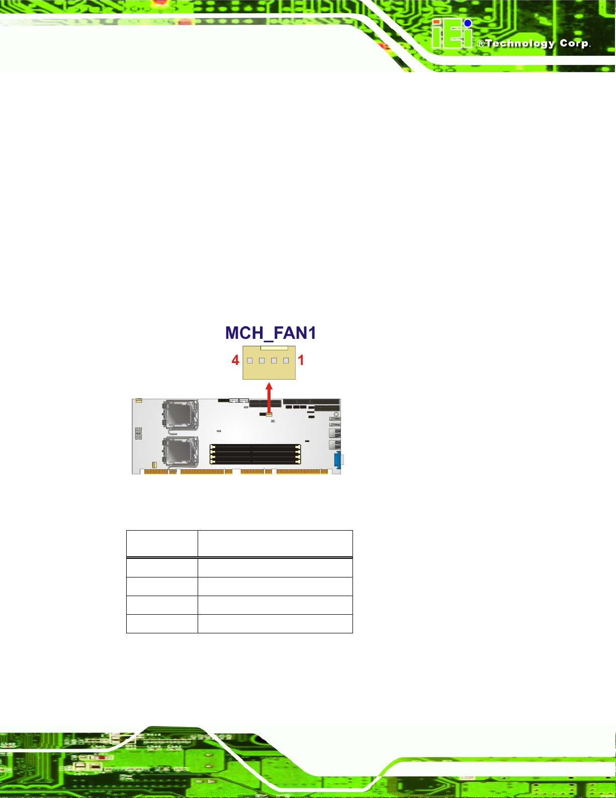
3.2.3 Cooling Fan Connector (Northbridge)
CN Label:
CN Type:
CN Location:
CN Pinouts:
MCH_FAN1
4-pin header (1x4)
Figure 3-4
See
Table 3-5
See
The cooling fan connector provides a 12V, 500mA current to a northbridge cooling fan.
The connector has a "rotation" pin to get rotation signals from fans and notify the system
so the system BIOS can recognize the fan speed. Please note that only specifie d fans can
issue the rotation signals.
Figure 3-4: +12V Fan Connector Location
PIN NO. DESCRIPTION
1 Ground
2 +12V
3 Rotation Signal
4 NC
Table 3-5: Northbridge Fan Connector Pinouts
Page 23
Page 38

3.2.4 CPU 12V Power Connector
CN Label: ATX_12V1
SPCIE-5100DX PICMG 1.3 CPU Card
CN Type:
CN Location:
CN Pinouts:
The connector supports the 12V power supply. To be able to turn on the system, the
ATX_12V1 connector must connect to a power supply.
Figure 3-5: CPU 12V Power Connector Location
8-pin headers (2x4)
See Figure 3-5
See Table 3-6
PIN NO. DESCRIPTION PIN NO. DESCRIPTION
1 GND 5 +12V
2 GND 6 +12V
3 GND 7 +12V
4 GND 8 +12V
Table 3-6: CPU 12V Power Connector Pinouts
3.2.5 Digital Input/Output (DIO) Connector
DIO1
10-pin header (2x5)
See Figure 3-6
Page 24
CN Label:
CN Type:
CN Location:
Page 39

SPCIE-5100DX PICMG 1.3 CPU Card
CN Pinouts:
See Table 3-7
The digital input/output connector is managed through a Super I/O chip. The DIO
connector pins are user programmable.
Figure 3-6: DIO Connector Location
PIN NO. DESCRIPTION PIN NO. DESCRIPTION
1 GND 2 VCC (+5V)
3 Output 3 4 Output 2
5 Output 1 6 Output 0
7 Input 3 8 Input 2
9 Input 1 10 Input 0
Table 3-7: DIO Connector Pinouts
3.2.6 Floppy Disk Connector (34-pin)
CN Label: FDD1
CN Type:
CN Location:
CN Pinouts:
The floppy disk connector is connected to a floppy disk drive.
34-pin header (2x17)
See Figure 3-7
See Table 3-8
Page 25
Page 40

SPCIE-5100DX PICMG 1.3 CPU Card
Figure 3-7: 34-pin FDD Connector Location
PIN NO. DESCRIPTION PIN NO. DESCRIPTION
1 GND 2 REDUCE WRITE
3 GND 4 N/C
5 N/C 6 N/C
7 GND 8 INDEX#
9 GND 10 MOTOR ENABLE A#
11 GND 12 DRIVE SELECT B#
13 GND 14 DRIVE SELECT A#
15 GND 16 MOTOR ENABLE B#
17 GND 18 DIRECTION#
19 GND 20 STEP#
21 GND 22 WRITE DATA#
23 GND 24 WRITE GATE#
25 GND 26 TRACK 0#
27 GND 28 WRITE PROTECT#
29 GND 30 READ DATA#
31 GND 32 SIDE 1 SELECT#
33 GND 34 DISK CHANGE#
Table 3-8: 34-pin FDD Connector Pinouts
Page 26
Page 41

SPCIE-5100DX PICMG 1.3 CPU Card
3.2.7 Front Panel Connector (14-pin)
CN Label:
CN Type:
CN Location:
CN Pinouts:
F_PANEL1
14-pin header (2x7)
Figure 3-8
See
Table 3-9
See
The front panel connector connects to external switches and indicators to monitor and
controls the motherboard. These indicators and switches include:
Power LED
Speaker
Power button
Reset
HDD LED
Figure 3-8: Front Panel Connector Pinout Locations (14-pin)
FUNCTION PIN DESCRIPTION FUNCTION PIN DESCRIPTION
Power LED
1 PWRLED+ 2 SPEAKER+
3 N/C 4 N/C
5 PWRLED-
Speaker
6 N/C
Page 27
Page 42

7 PWRBTN+ 8 SPEAKER- Power
SPCIE-5100DX PICMG 1.3 CPU Card
Button
9 PWRBTN- 10 N/C
11 HDDLED+ 12 RESET+ HDD LED
13 HDDLED-
Reset
14 RESET-
Table 3-9: Front Panel Connector Pinouts (14-pin)
3.2.8 Infrared Interface Connector (5-pin)
CN Label: IR1
CN Type:
CN Location:
CN Pinouts:
The infrared interface connector supports both Serial Infrared (SIR) and Amplitude Shift
Key Infrared (ASKIR) interfaces. To use the infrared port, configure COM2 as SIR or
ASKIR model in BIOS (see Section
5-pin header (1x5)
See Figure 3-9
See Table 3-10
5.3.4). By doing this, the normal RS-232 COM 2 will
be disabled.
Figure 3-9: Infrared Connector Pinout Locations
PIN NO. DESCRIPTION
1 VCC (+5V)
2 N/C
3 IR-RX
Page 28
Page 43

SPCIE-5100DX PICMG 1.3 CPU Card
PIN NO. DESCRIPTION
4 GND
5 IR-TX
Table 3-10: Infrared Connector Pinouts
3.2.9 Keyboard Connector
CN Label:
CN Type:
CN Location:
CN Pinouts:
KB1
5-pin header (1x5)
Figure 3-10
See
Table 3-11
See
The keyboard connector can be connected to a standard PS/2 cable or PS/2 cable to add
keyboard functionality to the system.
Figure 3-10: Keyboard Connector Location
PIN NO. DESCRIPTION
1 KEYBOARD CLOCK
2 KEYBOARD DATA
3 N/C
4 GROUND
5 VCC
Table 3-11: Keyboard Connector Pinouts
Page 29
Page 44

3.2.10 Mouse Connector
SPCIE-5100DX PICMG 1.3 CPU Card
CN Label:
CN Type:
CN Location:
CN Pinouts:
MS1
5-pin header (1x5)
Figure 3-10
See
Table 3-11
See
The mouse connector can be connected to a standard PS/2 cable or PS/2 cable to add
mouse functionality to the system.
Figure 3-11: Mouse Connector Location
PIN NO. DESCRIPTION
1 Mouse CLOCK
2 Mouse DATA
3 N/C
4 GROUND
5 VCC
Table 3-12: Mouse Connector Pinouts
Page 30
Page 45

SPCIE-5100DX PICMG 1.3 CPU Card
3.2.11 Parallel Port Connector
CN Label: LPT1
CN Type:
CN Location:
CN Pinouts:
26-pin box header
See Figure 3-12
See Table 3-13
The 26-pin parallel port connector connects to a parallel port connector interface or some
other parallel port device such as a printer.
Figure 3-12: Parallel Port Connector Location
PIN NO. DESCRIPTION PIN NO. DESCRIPTION
1 STROBE# 14 AUTO FORM FEED #
2 DATA0 15 ERROR#
3 DATA1 16 INITIALIZE#
4 DATA2 17 PRINTER SELECT LN#
5 DATA3 18 GND
6 DATA4 19 GND
7 DATA5 20 GND
8 DATA6 21 GND
9 DATA7 22 GND
10 ACKNOWLEDGE# 23 GND
11 BUSY 24 GND
12 PAPER EMPTY 25 GND
13 PRINTER SELECT
Table 3-13: Parallel Port Connector Pinouts
Page 31
Page 46

3.2.12 SATA Drive Connectors
SPCIE-5100DX PICMG 1.3 CPU Card
CN Label:
CN Type:
CN Location:
CN Pinouts:
SA TA1, SATA2, SATA3, SATA4, SATA5 and SATA6
7-pin SATA drive connectors
Figure 3-13
See
Table 3-14
See
The SATA drive connectors are each connected to a second generation SATA drive.
Second generation SATA drives transfer data at speeds as high as 3.0 Gb/s. The SATA
drives can be configured in a RAID configuration and support RAID 0, 1, 5 and 10.
Page 32
Figure 3-13: SATA Drive Connector Locations
PIN NO. DESCRIPTION
1 GND
2 TX+
3 TX4 GND
5 RX6 RX+
7 GND
Table 3-14: SATA Drive Connector Pinouts
Page 47

SPCIE-5100DX PICMG 1.3 CPU Card
3.2.13 Serial Port Connector (COM1, COM 2)
CN Label:
CN Type:
CN Location:
CN Pinouts:
COM1 and COM2
10-pin box header (2x5)
Figure 3-14
See
Table 3-15
See
The 10-pin serial port connector provides a RS-232 serial communications channel. The
serial port connector can be connected to external RS-232 serial port devices.
Figure 3-14: Serial Connector Pinout Locations
PIN NO. DESCRIPTION PIN NO. DESCRIPTION
1 DCD# 2 DSR#
3 RXD 4 RTS#
5 TXD 6 CTS#
7 DTR# 8 RI#
9 GND 10 NC
Table 3-15: Serial Connector Pinouts
Page 33
Page 48

3.2.14 SPI Flash Connector
CN Label: JSPI1
SPCIE-5100DX PICMG 1.3 CPU Card
CN Type:
CN Location:
CN Pinouts:
The 8-pin SPI Flash connector is used for the BIOS.
Figure 3-15: SPI Flash Connector Pinouts
8-pin header (2x4)
See Figure 3-15
See Table 3-16
PIN DESCRIPTION PIN DESCRIPTION
1 3.3V 2 GND
3 CS0 4 CLOCK
5 SO0 6 SI
7 N/C 8 N/C
Table 3-16: SPI Flash Connector
3.2.15 USB Connectors (Internal)
CN Label:
CN Type:
CN Location:
USB23, USB45 and USB67
8-pin header (2x4)
Figure 3-16
See
Page 34
Page 49

SPCIE-5100DX PICMG 1.3 CPU Card
Table 3-17
CN Pinouts:
See
The 2x4 USB pin connectors each provide connectivity to two USB 1.1 or two USB 2.0
ports. Each USB connector can support two USB devices. Additional external USB ports
are found on the rear panel. The USB ports are used for I/O bus expansion.
Figure 3-16: USB Connector Pinout Locations
PIN NO. DESCRIPTION PIN NO. DESCRIPTION
1 VCC (+5V) 2 GND
3 DATA- 4 DATA+
5 DATA+ 6 DATA7 GND 8 VCC (+5V)
Table 3-17: USB Port Connector Pinouts
3.3 External Peripheral Interface Connector Panel
The figure below shows the external peripheral interface connector (EPIC) panel. The
SPCIE-5100DX EPIC panel consists of the following:
2 x RJ-45 LAN connectors
2 x USB connectors
1 x VGA connector
Page 35
Page 50

Figure 3-17: SPCIE-5100DX External Peripheral Interface Connector
3.3.1 LAN Connectors
SPCIE-5100DX PICMG 1.3 CPU Card
CN Label:
CN Type:
CN Location:
CN Pinouts:
The SPCIE-5100DX is equipped with two built-in RJ-45 Ethernet controllers. The
controllers can connect to the LAN through two RJ-45 LAN connectors. There are two
LEDs on the connector indicating the status of LAN. The pin assignments are listed in the
following table:
PIN DESCRIPTION PIN
1 MDIA3- 5 MDIA1+
2 MDIA3+ 6 MDIA2+-
3. MDIA2- 7 MDIA0-
4. MDIA1- 8 MDIA0+
LAN1 and LAN2
RJ-45
Figure 3-17
See
Table 3-18
See
DESCRIPTION
Table 3-18: LAN Pinouts
Page 36
Page 51

SPCIE-5100DX PICMG 1.3 CPU Card
Figure 3-18: RJ-45 Ethernet Connector
The RJ-45 Ethernet connector has two status LEDs, one green and one yello w. The green
LED indicates activity on the port and the yellow LED indicates the port is linked. See
Table 3-19.
SPEED LED ACT/LINK LED
STATUS
OFF 10 Mbps LAN OFF OFF
Green 100 Mbps LAN YELLOW Linked
ORANGE 1000 Mbps LAN BLINKING Data Activity
DESCRIPTION STATUS
STATUS
Table 3-19: RJ-45 Ethernet Connector LEDs
3.3.2 USB Connector
CN Label:
CN Type:
CN Location:
CN Pinouts:
The SPCIE-5100DX has four external USB 2.0 ports. The ports connect to both USB 2.0
and USB 1.1 devices.
USB_C0 and USB_C1
USB port
Figure 3-17
See
Table 3-20
See
PIN NO. DESCRIPTION
1 VCC
2 DATA3 DATA+
Page 37
Page 52

PIN NO. DESCRIPTION
4 GROUND
Table 3-20: USB Port Pinouts
3.3.3 VGA Connector
SPCIE-5100DX PICMG 1.3 CPU Card
CN Label:
CN Type:
CN Location:
CN Pinouts:
VGA1
15-pin Female
Figure 3-17
See
Figure 3-19 and Table 3-21
See
The SPCIE-5100DX has a single 15-pin female connector for connectivity to standard
display devices.
Figure 3-19: VGA Connector
Page 38
PIN DESCRIPTION PIN DESCRIPTION
1 RED 2 GREEN
3 BLUE 4 NC
5 GND 6 GND
7 GND 8 GND
9 VCC 10 GND
11 NC 12 DDC DAT
13 HSYNC 14 VSYNC
15 DDCCLK
Table 3-21: VGA Connector Pinouts
Page 53
SPCIE-5100DX PICMG 1.3 CPU Card
Chapter
4
4 Installation
Page 39
Page 54

4.1 Anti-static Precautions
WARNING:
Failure to take ESD precautions during the installation of the
SPCIE-5100DX may result in permanent damage to the
SPCIE-5100DX and severe injury to the user.
Electrostatic discharge (ESD) can cause serious damage to electronic co mponents,
including the SPCIE-5100DX. Dry climates are especially susceptible to ESD. It is
therefore critical that whenever the SPCIE-5100DX, or any other electrical component is
handled, the following anti-static precautions are strictly adhered to.
SPCIE-5100DX PICMG 1.3 CPU Card
Wear an anti-static wristband: - Wearing a simple anti-static wristband can
help to prevent ESD from damaging the board.
Self-grounding:- Before handling the board touch any grounded conducting
material. During the time the board is handled, frequently touch any
conducting materials that are connected to the ground.
Use an anti-static pad: When configuring the SPCIE-5100DX, place it on an
antic-static pad. This reduces the possibility of ESD damaging the
SPCIE-5100DX.
Only handle the edges of the PCB:-: When handling the PCB, hold the PCB
by the edges.
Page 40
Page 55

SPCIE-5100DX PICMG 1.3 CPU Card
4.2 Installation Considerations
NOTE:
Failure to take ESD precautions during the installation of the
SPCIE-5100DX may result in permanent damage to the
SPCIE-5100DX and severe injury to the user.
Electrostatic discharge (ESD) can cause serious damage to electronic co mponents,
including the SPCIE-5100DX. Dry climates are especially susceptible to ESD. It is
therefore critical that whenever the SPCIE-5100DX, or any other electrical component is
handled, the following anti-static precautions are strictly adhered to.
Wear an anti-static wristband: - Wearing a simple anti-static wristband can
help to prevent ESD from damaging the board.
Self-grounding:- Before handling the board touch any grounded conducting
material. During the time the board is handled, frequently touch any
conducting materials that are connected to the ground.
Use an anti-static pad: When configuring the SPCIE-5100DX, place it on an
antic-static pad. This reduces the possibility of ESD damaging the
SPCIE-5100DX.
Only handle the edges of the PCB:-: When handling the PCB, hold the PCB
by the edges.
Page 41
Page 56

4.3 Installation Considerations
NOTE:
The following installation notices and installation considerations should
be read and understood before installation. All installation notices must
be strictly adhered to. Failing to adhere to these precautions may lead
to severe damage and injury to the person performing the installation.
WARNING:
The installation instructions described in this manual should be
SPCIE-5100DX PICMG 1.3 CPU Card
carefully followed in order to prevent damage to the components and
injury to the user.
Before and during the installation please DO the following:
Read the user manual:
o The user manual provides a complete description of the SPCIE-5100DX
installation instructions and configuration options.
Wear an electrostatic discharge cuff (ESD):
o Electronic components are easily damaged by ESD. Wearing an ESD cuff
removes ESD from the body and helps prevent ESD damage.
Place the SPCIE-5100DX on an antistatic pad:
o When installing or configuring the motherboard, place it on an antistatic
pad. This helps to prevent potential ESD damage.
Turn all power to the SPCIE-5100DX off:
Page 42
o When working with the SPCIE-5100DX, make sure that it is disconnected
from all power supplies and that no electricity is being fed into the system.
Before and during the installation of the SPCIE-5100DX DO NOT:
Page 57
SPCIE-5100DX PICMG 1.3 CPU Card
Remove any of the stickers on the PCB board. These stickers are required for
warranty validation.
Use the product before verifying all the cables and power connectors are
properly connected.
Allow screws to come in contact with the PCB circuit, connector pins, or its
components.
4.4 CPU, CPU Cooling Kit and DIMM Installation
WARNING:
Do not run the CPU without a heatsink and fan. Without the heatsink
and fan, the high temperatures can destroy the CPU and other
components. CPUs marked as fanless don't need the fan, but still need
adequate ventilation.
The CPU, CPU cooling kit and DIMM are the most critical components of the
SPCIE-5100DX. If one of these components is not installed the SPCIE-5100DX cannot
run.
4.4.1 CPU Support List
The Intel® Xeon® processors listed below are supported by the SPCIE-5100DX.
Processor
Process
Number
L5430 45nm 2.66GHz 1333MHz 12MB 50W 4
L5420 45nm 2.5GHz 1333MHz 12MB 50W 4
L5410 45nm 2.33GHz 1333MHz 12MB 50W 4
L5408 45nm 2.13GHz 1066MHz 12MB 40W 4
L5320 65nm 1.86GHz 1066MHz 8MB 50W 4
Clock Speed
FSB (MHz) L2 Cache TDP Cores
(GHz)
L5318 65nm 1.6GHz 1066MHz 8MB 45W 4
L5310 65nm 1.6GHz 1066MHz 8MB 50W 4
L5248 45nm 3.0GHz 1333MHz 6MB 55W 2
Page 43
Page 58

L5240 45nm 3.0GHz 1333MHz 6MB 40W 2
L5238 45nm 2.66GHz 1333MHz 6MB 35W 2
L5215 45nm 1.86GHz 1066MHz 6MB 20W 2
E5450 45nm 3.0GHz 1333MHz 12MB 80W 4
E5440 45nm 2.83GHz 1333MHz 12MB 80W 4
E5410 45nm 2.33GHz 1333MHz 12MB 80W 4
E5405 45nm 2.0GHz 1333MHz 12MB 80W 4
E5345 65nm 2.33GHz 1333MHz 8MB 80W 4
E5335 65nm 2.0GHz 1333MHz 8MB 80W 4
E5320 65nm 1.86GHz 1066MHz 8MB 80W 4
E5310 65nm 1.6GHz 1066MHz 8MB 80W 4
E5240 45nm 3.0GHz 1333MHz 6MB 40W 2
E5220 45nm 2.33GHz 1333MHz 6MB 65W 2
E5205 65nm 1.86GHz 1066MHz 6MB 65W 2
SPCIE-5100DX PICMG 1.3 CPU Card
E5160 65nm 3.0GHz 1333MHz 4MB 80W 2
E5150 65nm 2.66GHz 1333MHz 4MB 65W 2
5148 65nm 2.33GHz 1333MHz 4MB 40W 2
5140 65nm 2.33GHz 1333MHz 4MB 65W 2
5138 65nm 2.13GHz 1066MHz 4MB 35W 2
5130 65nm 2.0GHz 1333MHz 4MB 65W 2
5128 65nm 1.86GHz 1066MHz 4MB 40W 2
5120 65nm 1.86GHz 1066MHz 4MB 40W 2
5110 65nm 1.8GHz 1066MHz 4MB 65W 2
*The shaded processors are long-term support processors.
Table 4-1: Intel® Xeon® Processor Support List
Page 44
Page 59

SPCIE-5100DX PICMG 1.3 CPU Card
4.4.2 Socket LGA771 CPU Installation
WARNING:
CPUs are expensive and sensitive components. When installing the
CPU please be careful not to damage it in anyway. Make sure the CPU
is installed properly and ensure the correct cooling kit is properly
installed.
The LGA771 socket is shown in Figure 4-1.
Figure 4-1: Intel LGA771 Socket
To install the CPU, follow the steps below.
WARNING:
DO NOT touch the pins at the bottom of the CPU. When handling the
CPU, only hold it on the sides.
Step 1: Remove the protective cover. The black protective cover can be removed by
pulling up on the tab labeled "Remove". See
Figure 4-2.
Page 45
Page 60

Figure 4-2: Remove Protective Cover
Step 2: Open the socket. Disengage the load lever by pressing the lever down and
slightly outward to clear the retention tab. Fully open the lever, then open the
SPCIE-5100DX PICMG 1.3 CPU Card
load plate. See
Figure 4-3: CPU Socket Load Plate
Step 3: Inspect the CPU socket. Make sure there are no bent pins and make sure the
socket contacts are free of foreign material. If any debris is found, remove it with
compressed air.
Figure 4-3.
Page 46
Step 4: Orientate the CPU properly. The contact array should be facing the CPU
socket.
Page 61

SPCIE-5100DX PICMG 1.3 CPU Card
Step 5: Correctly position the CPU. Match the Pin 1 mark with the cut edge on the
CPU socket.
Step 6: Align the CPU pins. Locate pin 1 and the two orient ation notches on the CPU.
Carefully match the two orientation notches on the CPU with the socket
alignment keys.
Step 7: Insert the CPU. Gently insert the CPU into the socket. If the CPU pins are
properly aligned, the CPU should slide into the CPU socket smoothly. See
Figure 4-4.
Figure 4-4: Insert the Socket LGA771 CPU
Step 8: Close the CPU socket. Close the load plate and engage the load lever by
pushing it back to its original position. There will be some resist ance, but will not
require extreme pressure.
Step 9: Connect the 12 V power to the board. Connect the 12 V power from the power
supply to the CPU power connector (
Figure 4-5). Step 0:
Page 47
Page 62

Figure 4-5: CPU 12V Power Connector
4.4.3 Cooling Kit Installation
SPCIE-5100DX PICMG 1.3 CPU Card
Figure 4-6: IEI LGA771 Cooling Kit
Two IEI LGA771 CPU cooling kits (
cooling kit comprises a CPU heat sink and a cooling fan. To install the cooling kit, please
follow the steps below.
Step 1: Remove the four retention screws located near the LGA771 CPU sockets.
Figure 4-6) are shipped with the SPCIE-5100DX. The
NOTE:
The SPCIE-5100DX has a SBC support bracket on the bottom and the
bracket is secured to the board with few retention screws. The SBC support
bracket is to support the CPU cooling fan and the SPCIE-5100DX. To
install the CPU cooling fan, the four retention screws near the CPU sockets
need to be removed.
Page 48
Page 63

SPCIE-5100DX PICMG 1.3 CPU Card
Figure 4-7: CPU Fan Installation – Retention Screws Removal
Step 2: Spread a proper amount of thermal paste onto the bottom of the cooling fan
heat sink. The thermal paste between the CPU and the heat sink is import ant for
optimum heat dissipation.
Step 3: Place the cooling kit onto the CPU and properly align the cooling kit. Make
sure the CPU cooling fan cable can be properly routed when the cooling kit is
installed and its four spring screw fasteners can p a ss through the pre-drilled
holes on the PCB and the SBC support bracket.
Step 4: Secure the cooling kit to the board and the SBC support bracket. Use a
screwdriver to tighten the four screws. Tighten each nut a few turns at a time
and do not over-tighten the screws. (See
Step 5: Connect the fan cable. Connect the cooling kit fan cable to the fan connector
on the motherboard. Carefully route the cable and avoid heat generating chips
and fan blades.
Figure 4-8)
Page 49
Page 64

SPCIE-5100DX PICMG 1.3 CPU Card
Figure 4-8: CPU Fan Installation – First
Step 6: Repeat Step 3 ~ Step 6 to install the other CPU cooling fan. See
Step 0:
Figure 4-9.
Page 50
Figure 4-9: CPU Fan Installation – Second
Page 65
SPCIE-5100DX PICMG 1.3 CPU Card
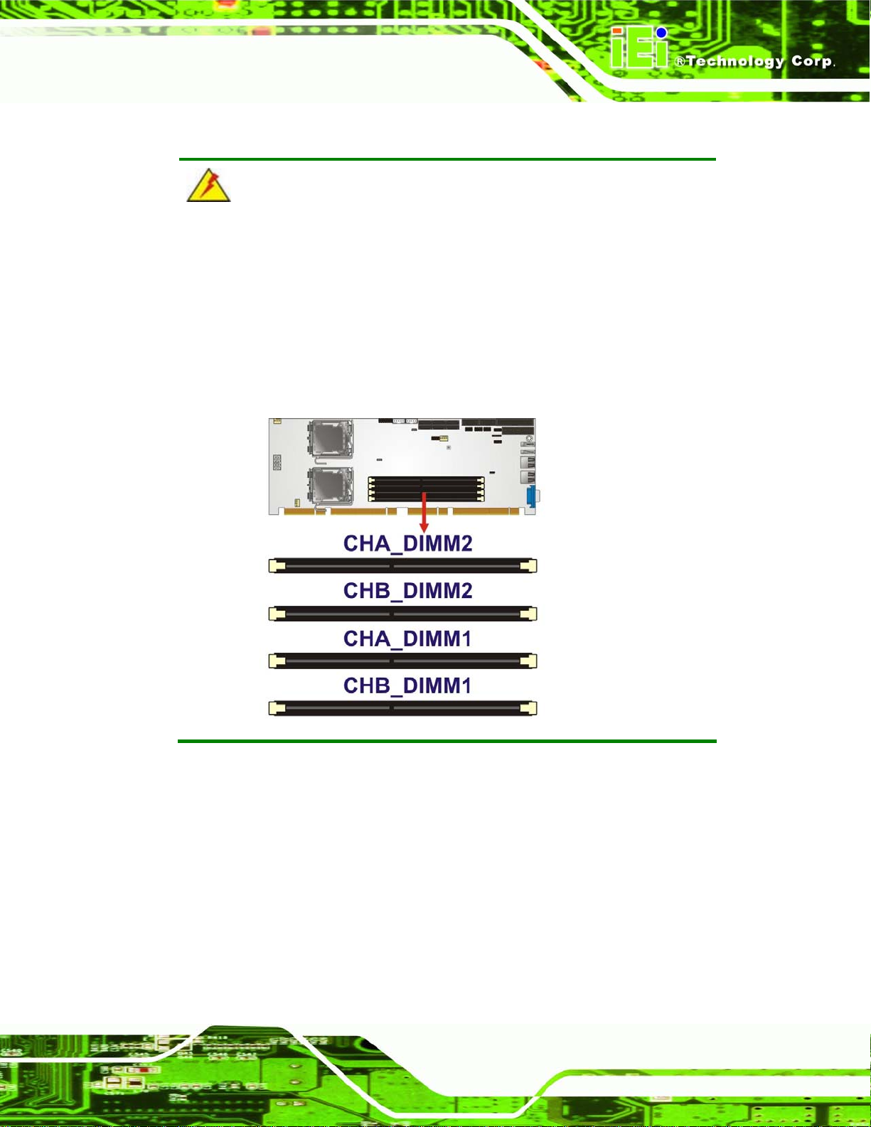
4.4.4 DIMM Installation
WARNING:
To be able to turn on the SPCIE-5100DX, either the CHA_DIMM1 or the
CHB_DIMM1 socket must install with an ECC Registered DDR2 DIMM. To
install a second DIMM, install in the socket that is at the same channel with
the first DIMM. For example, the first DIMM is installed in CHA_DIMM1
then the second DIMM should be installed in the CHA_DIMM2. The DIMM
socket locations are shown below.
To install a DIMM into a DIMM socket, please follow the steps below and refer to
Figure 4-10.
Page 51
Page 66

SPCIE-5100DX PICMG 1.3 CPU Card
Figure 4-10: Installing a DIMM
Step 1: Open the DIMM socket handles. The DIMM socket has two handles that secure
the DIMM into the socket. Before the DIMM can be inserted into the socket, the
handles must be opened. See
Step 2: Align the DIMM with the socket. The DIMM must be oriented in such a way that
the notch in the middle of the DIMM must be aligned with the plasti c bridge in the
socket. See
Step 3: Insert the DIMM. Once properly aligned, the DIMM can be inserted into the
socket. As the DIMM is inserted, the white handles on the side of the socket will
close automatically and secure the DIMM to the socket. See
Step 4: Removing a DIMM. To remove a DIMM, push both handles outward. The
memory module is ejected by a mechanism in the socket.Step 0:
Figure 4-10.
Figure 4-10.
Figure 4-10.
Page 52
Page 67

SPCIE-5100DX PICMG 1.3 CPU Card
4.5 Jumper Settings
NOTE:
A jumper is a metal bridge that is used to
close an electrical circuit. It consists of
two metal pins and a small metal clip
(often protected by a plastic cover) that
slides over the pins to connect them.
To CLOSE/SHORT a jumper means
connecting the pins of the jumper with
the plastic clip and to OPEN a jumper
means removing the plastic clip from a
jumper.
Before the SPCIE-5100DX is installed in the system, the jumpers must be set in
accordance with the desired configuration. The jumpers on the SPCIE-5100DX are listed
in
Table 4-2.
Description Label Type
Clear CMOS J_CMOS1 3-pin header
Table 4-2: Jumpers
Jumper
4.5.1 Clear CMOS Jumper
Jumper Label:
Jumper Type:
Jumper Settings:
Jumper Location:
If the SPCIE-5100DX fails to boot due to improper BIOS settings, the clear CMOS jumper
clears the CMOS data and resets the system BIOS information. To do this, use the jumper
J_CMOS1
3-pin header
Table 4-3
See
Figure 4-11
See
Page 53
Page 68

SPCIE-5100DX PICMG 1.3 CPU Card
cap to close pins 2 and 3 for a few seconds then reinstall the jumper clip back to pins 1
and 2.
If the “CMOS Settings Wrong” message is displayed during the boot up process, the fault
may be corrected by pressing the F1 to enter the CMOS Setup menu. Do one of the
following:
Enter the correct CMOS setting
Load Optimal Defaults
Load Failsafe Defaults.
After having done one of the above, save the changes and exit the CMOS Setup menu.
The clear CMOS jumper settings are shown in
Jumper Select Description
Short 1 - 2 Keep CMOS Setup Default
Short 2 - 3 Clear CMOS Setup
Table 4-3.
Table 4-3: Clear CMOS Jumper Settings
The location of the clear CMOS jumper is shown in Figure 4-11 below.
Page 54
Figure 4-11: Clear CMOS Jumper
Page 69

SPCIE-5100DX PICMG 1.3 CPU Card
4.6 Chassis Installation
4.6.1 Airflow
WARNING:
Airflow is critical to the cooling of the CPU and other on-board
components. The chassis in which the SPCIE-5100DX must have air
vents to allow cool air to move into the system and hot air to move out.
The SPCIE-5100DX must be installed in a chassis with ventilation holes on the sides
allowing airflow to travel through the heat sink surface. In a system with an individual
power supply unit, the cooling fan of a power supply can also help generate airflow
through the board surface.
NOTE:
IEI has a wide range of backplanes available. Please contact your
SPCIE-5100DX vendor, reseller or an IEI sales representative at
sales@iei.com.tw or visit the IEI website (http://www.ieiworld.com.tw)
to find out more about the available chassis.
4.6.2 Backplane Installation
Before the SPCIE-5100DX can be installed into the chassis, a backplane must first be
installed. Please refer to the installation instructions that came with the backplane and the
chassis to see how to install the backplane into the chassis.
Page 55
Page 70

SPCIE-5100DX PICMG 1.3 CPU Card
NOTE:
IEI has a wide range of backplanes available (Refer to Section 1.7.2).
Please contact your SPCIE-5100DX vendor, reseller or an IEI sales
representative at
(
http://www.ieiworld.com.tw) to find out more about the available
chassis.
sales@iei.com.tw or visit the IEI website
4.6.3 CPU Card Installation
To install the SPCIE-5100DX CPU card onto the backplane, carefully align the CPU card
interface connectors with the corresponding socket on the backplane. To do this, please
refer to the reference material that came with the backplane. Next, secure the CPU card to
the chassis. To do this, please refer to the reference material that came with the chassis.
4.7 Internal Peripheral Device Connections
4.7.1 Audio Kit Installation (Optional)
An optional audio kit that is separately ordered connects to the 9-pin audio connector on
the SPCIE-5100DX. The audio kit consists of five audio jacks. One audio jack, Mic In,
Page 56
connects to a microphone. The remaining four audio jacks, Front-In, Front-Out, Rear-Out
and subwoofer connect to four speakers including a subwoofer. To install the audio kit,
please refer to the steps below:
Step 1: Locate the audio connector. The location of the 10-pin audio connector is shown
in Chapter 3.
Step 2: Align pin 1. Align pin 1 on the on-board connector with pin 1 on the audio kit
connector. Pin 1 on the audio kit connector is indicated with a white dot. See
Figure 4-12.
Page 71
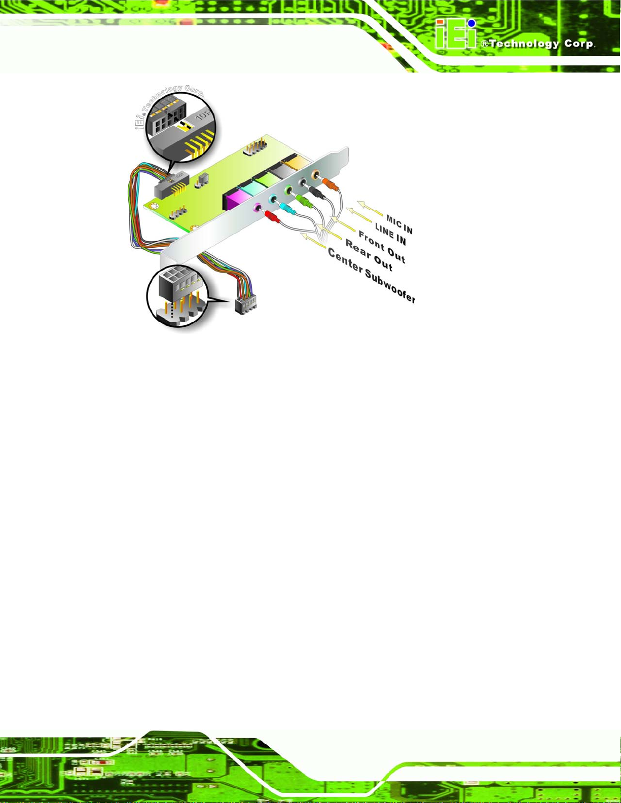
SPCIE-5100DX PICMG 1.3 CPU Card
Figure 4-12: Audio Kit Connection
Step 3: Connect the audio devices. Connect the speakers and the subwoofer to the
appropriate audio jack shown in
Figure 4-12.Step 0:
4.7.2 FDD Cable Connection (Optional)
The FDD flat cable connects to the SPCIE-5100DX to one FDD device. To connect an
FDD to the SPCIE-5100DX please follow the instructions below.
Step 1: Locate the FDD connector. The location of the FDD device connecto r is shown
in Chapter 3.
Step 2: Insert the connector. Connect the FDD cable connector to the on-board
connector. See
can only be inserted in one direction.
Figure 4-13. A key on the front of the cable connector ensures it
Page 57
Page 72

SPCIE-5100DX PICMG 1.3 CPU Card
Figure 4-13: FDD Cable Connection
Step 3: Connect the cable to an FDD devi ce. Connect the co nnector at the other end
of the cable to an FDD device. Make sure that pin 1 on the cable corresponds to
pin 1 on the connector.Step 0:
4.7.3 Keyboard and Mouse PS/2 Cable with Bracket (Optional)
The SPCIE-5100DX can be shipped with an optional keyboard and mouse PS/2 cabl e
with bracket. The keyboard and mouse PS/2 cable with bracket comprise s of two PS/2
connectors installed on a bracket. Each PS/2 connector is connected via a cable to two
separate female 5-pin wafer connectors. The female 5-pin wafer connectors are
connected to the corresponding on-board keyboard and mouse connector. To connect the
optional keyboard and mouse PS/2 cable with bracket please follow the steps below.
Step 1: Locate the connectors. The locations of the keyboard connector and the mouse
Page 58
connector are shown in Chapter 3.
Step 2: Align the connectors. Correctly align pin 1 on the PS/2 keyboard (mouse) cable
connector with pin 1 on the SPCIE keyboard (mouse) connector. See
Figure
Page 73
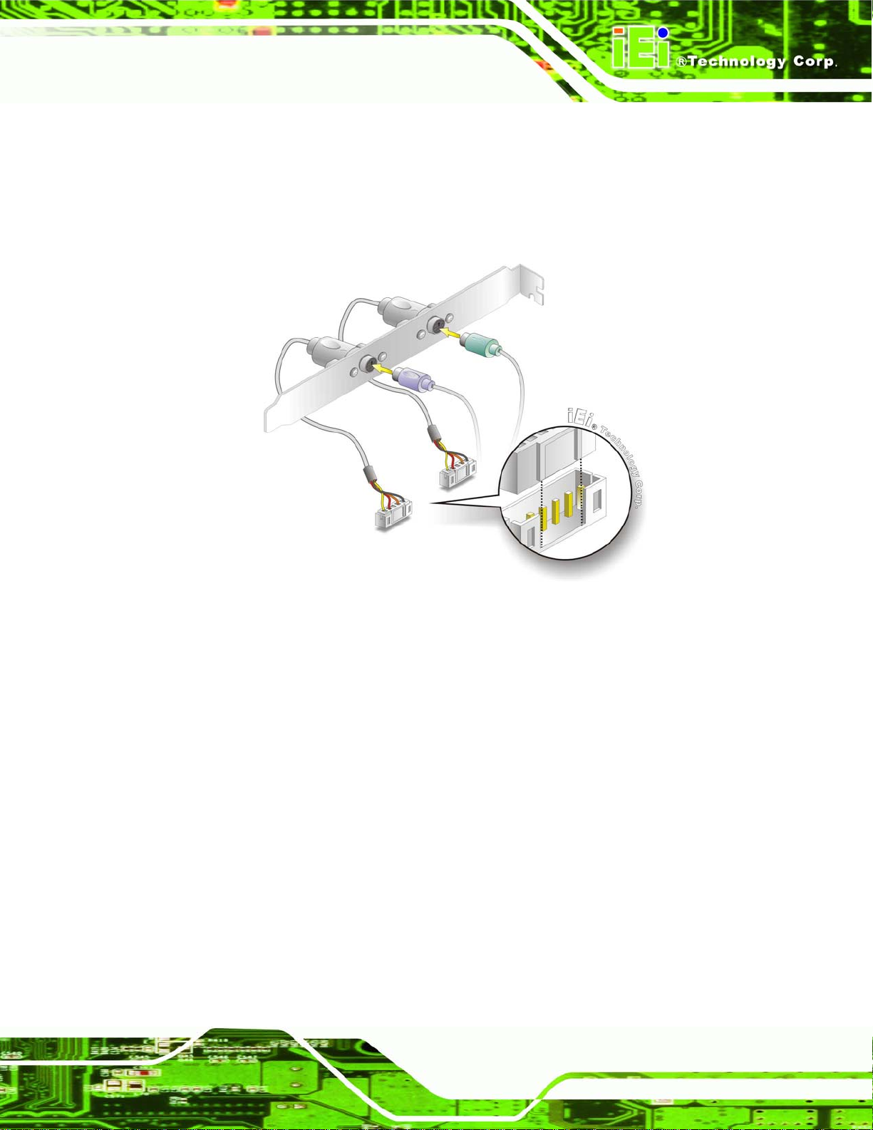
SPCIE-5100DX PICMG 1.3 CPU Card
4-14.
Step 3: Insert the cable connectors. Once the keyboard (mou se) cable connector is
properly aligned with the keyboard (mouse) connector on the SPCIE-5100DX,
connect the cable connector to the on-board connector. See
Figure 4-14: Keyboard and Mouse PS/2 Cable with Bracket
Figure 4-14.
Step 4: Connect the bracket to the chassis. The bracket has a retention screw hole at
the top. Properly insert the bracket into the chassis and secure th e bracket to the
chassis with a retention screw passing through the retention screw hole. Please
see the chassis installation inst ructions for more details.
Step 5: Connect the keyboard and mouse. Once the PS/2 connectors are connected to
the chassis, a keyboard and mouse can each be connected to one of the PS/2
connectors. See
connector are both marked. Please make sure the keyboard and mouse are
connected to the correct PS/2 connector. Step 0:
Figure 4-14.The keyboard PS/2 connector and mouse PS/2
Page 59
Page 74

SPCIE-5100DX PICMG 1.3 CPU Card
Figure 4-15: PS/2 Connector
4.7.4 Dual RS-232 Cable Connection
The dual RS-232 cable consists of two connectors attached to two independent cables.
Each cable is then attached to a D-sub 9 male connector that is mounted onto a bracket.
To install the dual RS-232 cable, please follow the steps below.
Step 1: Locate the connectors. The locations of the RS-232 connectors are shown in
Chapter 3.
Step 2: Insert the cable connectors. Insert one connector into each serial port box
headers. See
the connector can only be installed in one direction.
Figure 4-16. A key on the front of the cable connectors ensures
Page 60
Page 75

SPCIE-5100DX PICMG 1.3 CPU Card
Figure 4-16: Dual RS-232 Cable Installation
Step 3: Secure the bracket. The dual RS-232 connector has two D-sub 9 male
connectors secured on a bracket. To secure the bracket to the chassis please
refer to the reference material that came with the chassis. Step 0:
4.7.5 Parallel Port Cable with Slot Bracket (Optional)
The optional parallel port (LPT) cable respectively connects the on-board LPT 26-pin box
header to an external LPT device (like a printer). The cable comprise s a 26-pin female
header, to be connected to the on-board LPT box-header, on one side and on the other
side a standard external LPT connector. To connect the LPT cable, please follow the
steps below.
Step 1: Locate the connector. The LPT connector location is shown in Chapter 4.
Step 2: Align the connectors. Correctly align pin 1 on the cable connector with pin 1 on
the SPCIE-5100DX LPT box-header connector. See
Figure 4-17.
Page 61
Page 76

Step 3: Insert the cable connectors. Once th e cable conn ector i s pro perly aligne d wit h
the 26-pin box-header connector on the SPCIE-5100DX, connect t he cable
SPCIE-5100DX PICMG 1.3 CPU Card
connector to the on-board connector. See
Figure 4-17: LPT Cable Connection
Step 4: Attach the LPT connector brack et to the chassis. The LPT cabl e connector is
connected to a standard external LPT interface connector. To secure the LPT
Figure 4-17.
interface connector to the chassis please refer to the installation instructions that
came with the chassis.
Step 5: Connect LPT device. Once the LPT interface connector is connected to the
chassis, the LPT device can be connected to the LPT interface connector. See
Figure 4-18 Step 0:\
Page 62
Page 77

SPCIE-5100DX PICMG 1.3 CPU Card
Figure 4-18: Connect the LPT Device
4.7.6 SATA Drive Connection
The SPCIE-5100DX is shipped with two SATA drive cables and one SATA drive power
cable. To connect the SATA drives to the connectors, please follow the steps below.
Step 1: Locate the connectors. The locations of the SATA drive connectors are shown in
Chapter 3.
Step 2: Insert the cable connector. Press the clip on the connector at the end of the
SATA cable and insert the cable connector into the on-board SATA drive
connector. See
Figure 4-19.
Page 63
Page 78

SPCIE-5100DX PICMG 1.3 CPU Card
Figure 4-19: SATA Drive Cable Connection
Step 3: Connect the cable to the SATA disk. Connect the connector on the other end of
the cable to the connector at the back of the SATA drive. See
Step 4: Connect the SATA power cable. Connect the SATA power connector to the back
of the SATA drive. See
Figure 4-20. Step 0:
Figure 4-20.
Page 64
Figure 4-20: SATA Power Drive Connection
Page 79

SPCIE-5100DX PICMG 1.3 CPU Card
4.7.7 USB Cable (Dual Port)
The SPCIE-5100DX is shipped with a dual port USB 2.0 cable. To connect the USB cable
connector, please follow the steps below.
Step 1: Locate the connectors. The locations of the USB connectors are shown in
Chapter 3.
WARNING:
If the USB pins are not properly aligned, the USB device can burn out.
Step 2: Align the connectors. The cable has two connectors. Correctly align pin 1on
each cable connector with pin 1 on the SPCIE-5100DX USB connector.
Step 3: Insert the cable connectors. Once the cable conne ctors are properly aligned
with the USB connectors on the SPCIE-5100DX, connect the cable connectors
to the on-board connectors. See
Figure 4-21.
Figure 4-21: Dual USB Cable Connection
Step 4: Attach the bracket to the chassis. The USB 2.0 conne ctors are attached to a
Page 65
Page 80
bracket. To secure the bracket to the chassis please refer to the inst allation
instructions that came with the chassis.Step 0:
SPCIE-5100DX PICMG 1.3 CPU Card
4.8 External Peripheral Interface Connection
The following external peripheral devices can be connected to the external peripheral
interface connectors.
RJ-45 Ethernet cable connectors
USB devices
VGA connector
To install these devices, connect the corresponding cable connector from the actual
device to the corresponding SPCIE-5100DX external peripheral interface connector
making sure the pins are properly aligned.
4.8.1 LAN Connection (Single Connector)
There are two external RJ-45 LAN connectors. The RJ-45 connectors enable connection
to an external network. To connect a LAN cable with an RJ-45 connector, please follow
the instructions below.
Step 1: Locate the RJ-45 connectors. The locations of the USB connectors are shown in
Chapter 4.
Step 2: Align the connectors. Align the RJ-45 connector on the LAN cable with one of
the RJ-45 connectors on the SPCIE-5100DX. See
Figure 4-22.
Page 66
Page 81

SPCIE-5100DX PICMG 1.3 CPU Card
Figure 4-22: LAN Connection
Step 3: Insert the LAN cable RJ-45 connector. Once aligned, gently insert the LAN cable
RJ-45 connector into the on-board RJ-45 connector. Step 0:
4.8.2 USB Device Connection (Single Connector)
There are two external USB 2.0 connectors. Both connectors are perpendicular to the
SPCIE-5100DX. To connect a USB 2.0 or USB 1.1 device, please follow the instructions
below.
Step 1: Located the USB connectors. The locations of the USB connectors are shown i n
Chapter 4.
Step 2: Align the connectors. Align the USB device connector with one of the connectors
on the SPCIE-5100DX. See
Figure 4-23.
Page 67
Page 82
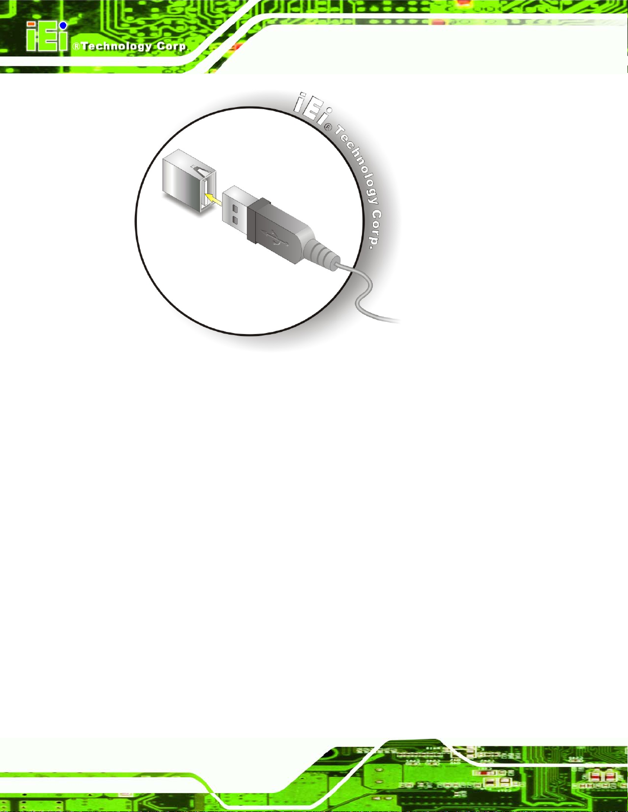
SPCIE-5100DX PICMG 1.3 CPU Card
Figure 4-23: USB Device Connection
Step 3: Insert the device connector. Once aligned, gently insert the USB device
connector into the on-board connector. Step 0:
4.8.3 VGA Monitor Connection
The SPCIE-5100DX has a single female DB-15 connector on the external peripheral
interface panel. The DB-15 connector is connected to a CRT or VGA monitor. To connect
a monitor to the SPCIE-5100DX, please follow the instructions below.
Step 1: Locate the female DB-15 connector. The location of the female DB-15 connector
is shown in Chapter 3.
Step 2: Align the VGA connector. Align the male DB-15 connector on the VGA screen
cable with the female DB-15 connector on the external peripheral interface.
Page 68
Step 3: Insert the VGA connector. Once the connectors are properly aligned with the
insert the male connector from the VGA screen into the female connector on the
SPCIE-5100DX. See
Figure 4-24.
Page 83

SPCIE-5100DX PICMG 1.3 CPU Card
Figure 4-24: VGA Connector
Step 4: Secure the connector. Secure the DB-15 VGA con nector from the VGA monitor
to the external interface by tightening the two retention screws on either side of
the connector. Step 0:
4.9 Connecting the SPCIE-5100DX to the Backplane
The SPCIE-5100DX is a PICMG 1.3 form factor CPU card. To install the SPCIE-5100DX
onto the backplane, please follow the instructions below.
Step 1: Align the edge connectors. Align the four edge connectors (labeled A, B, C and
D in
Figure 4-25) on the SPCIE-5100DX with the corresponding connectors on
the PICMG 1.3 backplane. See
Figure 4-25.
Page 69
Page 84

SPCIE-5100DX PICMG 1.3 CPU Card
Figure 4-25: SPCIE-5100DX Installation
Step 2: Insert the connectors. Gently push the CPU card onto the connectors making
sure the CPU card edge connectors are securely inserted into the
corresponding backplane connectors. Step 0:
Page 70
Page 85

SPCIE-5100DX PICMG 1.3 CPU Card
Chapter
5
5 BIOS Screens
Page 71
Page 86

5.1 Introduction
A licensed copy of AMI BIOS is preprogrammed into the ROM BIOS. The BIOS setup
program allows users to modify the basic system configuration. This chapter describes
how to access the BIOS setup program and the configuration options that may be
changed.
5.1.1 Starting Setup
The AMI BIOS is activated when the computer is turned on. The setup program can be
activated in one of two ways.
SPCIE-5100DX PICMG 1.3 CPU Card
1. Press the D
2. Press the D
message appears on the screen. 0.
If the message disappears before the D
again.
ELETE key as soon as the system is turned on or
ELETE key when the “Press Del to enter SETUP”
ELETE key is pressed, restart the computer and try
5.1.2 Using Setup
Use the arrow keys to highlight items, press ENTER to select, use the PageUp and
PageDown keys to change entries, press F1 for help and press E
keys are shown in.
Key Function
Up arrow Move to previous item
Down arrow Move to next item
Left arrow Move to the item on the left hand side
SC to quit. Navigation
Page 72
Right arrow Move to the item on the right hand side
Esc key Main Menu – Quit and not save changes into CMOS
Status Page Setup Menu and Option Page Setup Menu --
Exit current page and return to Main Menu
Page Up key Increase the numeric value or make changes
Page Dn key Decrease the numeric value or make changes
Page 87

SPCIE-5100DX PICMG 1.3 CPU Card
F1 key General help, only for St atus Page Setup Menu and Option
Page Setup Menu
F2 /F3 key Change color from total 16 colors. F2 to select color
forward.
F10 key Save all the CMOS changes, only for Main Menu
Table 5-1: BIOS Navigation Keys
5.1.3 Getting Help
When F1 is pressed a small help window describing the approp riate keys to use and the
possible selections for the highlighted item appears. To exit the Help Window press E
the F1 key again.
5.1.4 Unable to Reboot After Configuration Changes
If the computer cannot boot after changes to the system configuration is made, CMOS
defaults. Use the jumper described in Chapter 5.
5.1.5 BIOS Menu Bar
The menu bar on top of the BIOS screen has the following main items:
Main Changes the basic system configuration.
Advanced Changes the advanced system settings.
PCIPnP Changes the advanced PCI/PnP Settings
Boot Changes the system boot configuration.
Security Sets User and Supervisor Passwords.
Chipset Changes the chipset settings.
SC or
Power Changes power management settings.
Exit Selects exit options and loads default settings
The following sections completely describe the configuration options found in the menu
items at the top of the BIOS screen and listed above.
Page 73
Page 88
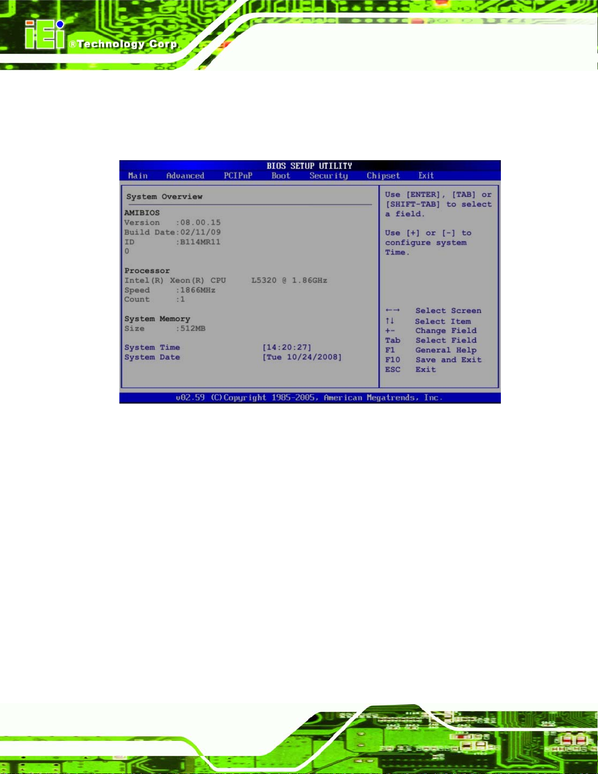
5.2 Main
The Main BIOS menu (BIOS Menu 1) appears when the BIOS Setup program is entered.
The Main menu gives an overview of the basic system information.
SPCIE-5100DX PICMG 1.3 CPU Card
BIOS Menu 1: Main
System Overview
The System Overvie w lists a brief summary of different system components. Th e fields in
System Overview cannot be changed. The items shown in the system overview include:
AMI BIOS: Displays auto-detected BIOS information
o Version: Current BIOS version
o Build Date: Date the current BIOS version was made
o ID: Installed BIOS ID
Processor: Displays auto-detected CPU specifications
o Type: Names the currently installed processor
o Speed: Lists the processor speed
o Count: The number of CPUs on the motherboard
System Memory: Displays the auto-detected system memory.
Page 74
Page 89

SPCIE-5100DX PICMG 1.3 CPU Card
o Size: Lists memory size
The System Overview field also has two user configurable fields:
System Time [xx:xx:xx]
Use the System Time option to set the system time. Manually enter the hours, minutes
and seconds.
System Date [xx/xx/xx]
Use the System Date option to set the system date. Manually enter the day, month and
year.
5.3 Advanced
Use the Advanced menu to configure the CPU and peripheral devices through the
following sub-menus:
WARNING:
Setting the wrong values in the sections below may cause the system
to malfunction. Make sure that the settings made are compatible with
the hardware.
CPU Configuration (see Section 5.3.1)
IDE Configuration (see Section 5.3.2)
Floppy Configuration (see Section 5.3.3)
SuperIO Configuration (see Section 5.3.4)
Hardware Health Configuration (see Section 5.3.5)
AHCI Configuration (see Section 5.3.6)
Remote Access Configuration (see Section 5.3.7)
USB Configuration (see Section 5.3.8)
Page 75
Page 90

SPCIE-5100DX PICMG 1.3 CPU Card
BIOS Menu 2: Advanced
5.3.1 CPU Configuration
Use the CPU Configuration menu (BIOS Menu 3) to view detailed CPU specifications and
configure the CPU.
Page 76
BIOS Menu 3: CPU Configuration
Page 91

SPCIE-5100DX PICMG 1.3 CPU Card
The CPU Configuration menu (BIOS Menu 3) lists the following CPU details:
Manufacturer: Lists the name of the CPU manufacturer
Brand String: Lists the brand name of the CPU being used
Frequency: Lists the CPU processing speed
FSB Speed: Lists the FSB speed
Cache L1: Lists the CPU L1 cache size
Cache L2: Lists the CPU L2 cache size
5.3.2 IDE Configuration
Use the IDE Configuration menu (BIOS Menu 4) to change and/or set the configuration
of the IDE devices installed in the system.
BIOS Menu 4: IDE Configuration
SATA#1 Configurations [Compatible]
Use the SATA Configurations option to configure the SATA controller.
Disabled
Disables the on-board ATA/IDE controller.
Page 77
Page 92

SPCIE-5100DX PICMG 1.3 CPU Card
Compatible
Enhanced D
Configure SATA as [IDE]
Use the Configure SATA as option to configure SATA devices as normal IDE devices.
IDE D
Configures the on-board ATA/IDE controller to be in
compatible mode. In this mode, a SATA channel will
replace one of the IDE channels. This mode supports up
to 4 storage devices.
Configures the on-board ATA/IDE controller to be in
Enhanced mode. In this mode, IDE channels and SATA
channels are separated. This mode supports up to 6
storage devices. Some legacy OS do not support this
mode.
EFAULT
EFAULT
Configures SATA devices as normal IDE device.
RAID
AHCI
SATA#2 Configurations [Enhanced]
Use the SATA Configurations option to configure the SATA controller.
Disabled
Enhanced D
Configures SATA devices as RAID device
Configures SATA devices as AHCI
Disables the on-board ATA/IDE controller.
EFAULT
Configures the on-board ATA/IDE controller to be in
Enhanced mode. In this mode, IDE channels and SATA
channels are separated. This mode supports up to 6
storage devices. Some legacy OS do not support this
mode.
Page 78
Page 93

SPCIE-5100DX PICMG 1.3 CPU Card
IDE Master and IDE Slave
When entering setup, BIOS auto detects the presence of IDE devices. BIOS displays the
status of the auto detected IDE devices. The following IDE devices are detected and are
shown in the IDE Configuration menu:
Primary IDE Master
Primary IDE Slave
Secondary IDE Master
Secondary IDE Slave
Third IDE Master
Fourth IDE Master
The IDE Configuration menu (
BIOS Menu 4) allows changes to the configurations for the
IDE devices installed in the system. If an IDE device is detected, and one of the above
listed four BIOS configuration options are selected, the IDE configuration options shown in
Section
5.3.2.1 appear.
5.3.2.1 IDE Master, IDE Slave and Serial-ATA Primary/Secondary Channel
Use the IDE Master and IDE Slave configuration menu to view both primary and
secondary IDE device details and configure the IDE devices connected to the system.
Page 79
Page 94

SPCIE-5100DX PICMG 1.3 CPU Card
BIOS Menu 5: IDE Master and IDE Slave Configuration
Auto-Detected Drive Parameters
The “grayed-out” items in the left frame are IDE disk drive parameters automatically
detected from the firmware of the selected IDE disk drive. The drive parameters are listed
as follows:
Device: Lists the device type (e.g. hard disk, CD-ROM etc.)
Type: Indicates the type of devices a user can manually select
Vendor: Lists the device manufacturer
Size: List the storage capacity of the device.
LBA Mode: Indicates whether the LBA (Logical Block Addressing) is a
method of addressing data on a disk drive is supported or not.
Block Mode: Block mode boosts IDE drive performance by increa sing the
amount of data transferred. Only 512 bytes of data can be transferred per
Page 80
interrupt if block mode is not used. Block mode allows transfers of up to 64 KB
per interrupt.
PIO Mode: Indicates the PIO mode of the installed device.
Async DMA: Indicates the highest Asynchronous DMA Mode that is
Page 95

SPCIE-5100DX PICMG 1.3 CPU Card
supported.
Ultra DMA: Indicates the highest Synchronous DMA Mode that is supported.
S.M.A.R.T.: Indicates whether or not the Self-Monitoring Analysis and
Reporting Technology protocol is supported.
32Bit Data Transfer: Enables 32-bit data transfer.
Type [Auto]
Use the Type BIOS option select the type of device the AMIBIOS attempts to boot from
after the Power-On Self-Test (POST) is complete.
Not Installed
Auto DEFAULT
CD/DVD
ARMD
BIOS is prevented from searching for an IDE disk
drive on the specified channel.
The BIOS auto detects the IDE disk drive type
attached to the specified channel. This setting should
be used if an IDE hard disk drive is attached to the
specified channel.
The CD/DVD option specifies that an IDE CD-ROM
drive is attached to the specified IDE channel. The
BIOS does not attempt to search for other types of
IDE disk drives on the specified channel.
This option specifies an ATAPI Removable Media
Device. These include, but are not limited to:
LBA/Large Mode [Auto]
Use the LBA/Large Mode option to disable or enable BIOS to auto detects LBA (Logical
Block Addressing). LBA is a method of addressing data on a disk drive. In LBA mode, the
maximum drive capacity is 137 GB.
ZIP
LS-120
Page 81
Page 96

SPCIE-5100DX PICMG 1.3 CPU Card
Disabled
Auto DEFAULT
Block (Multi Sector Transfer) [Auto]
Use the Block (Multi Sector Transfer) to disable or enable BIOS to auto detect if the
device supports multi-sector transfers.
Disabled
Auto DEFAULT
BIOS is prevented from using the LBA mode control on
the specified channel.
BIOS auto detects the LBA mode control on the specified
channel.
BIOS is prevented from using Multi-Sector Transfer on the
specified channel. The data to and from the device occurs
one sector at a time.
BIOS auto detects Multi-Sector Transfer support on the
drive on the specified channel. If supported the data
transfer to and from the device occurs multiple sectors at
a time.
PIO Mode [Auto]
Use the PIO Mode option to select the IDE PIO (Programmable I/O) mode program timing
cycles between the IDE drive and the programmable IDE controller. As the PIO mode
increases, the cycle time decrease s.
Auto DEFAULT
0
1
2
3
PIO mode 0 selected with a maximum transfer rate of 3.3MBps
PIO mode 1 selected with a maximum transfer rate of 5.2MBps
PIO mode 2 selected with a maximum transfer rate of 8.3MBps
PIO mode 3 selected with a maximum transfer rate of 11.1MBps
BIOS auto detects the PIO mode. Use this value if the IDE disk
drive support cannot be determined.
Page 82
Page 97

SPCIE-5100DX PICMG 1.3 CPU Card
4
DMA Mode [Auto]
Use the DMA Mode BIOS selection to adjust the DMA mode options.
Auto DEFAULT
SWDMA0
SWDMA1
PIO mode 4 selected with a maximum transfer rate of 16.6MBps
(This setting generally works with all hard disk drives
manufactured after 1999. For other disk drives, such as IDE
CD-ROM drives, check the specifications of the drive.)
BIOS auto detects the DMA mode. Use this value if the IDE
disk drive support cannot be determined.
Single Word DMA mode 0 selected with a maximum data
transfer rate of 2.1MBps
Single Word DMA mode 1 selected with a maximum data
SWDMA2
MWDMA0
MWDMA1
MWDMA2
UDMA1
UDMA1
transfer rate of 4.2MBps
Single Word DMA mode 2 selected with a maximum data
transfer rate of 8.3MBps
Multi Word DMA mode 0 selected with a maximum data
transfer rate of 4.2MBps
Multi Word DMA mode 1 selected with a maximum data
transfer rate of 13.3MBps
Multi Word DMA mode 2 selected with a maximum data
transfer rate of 16.6MBps
Ultra DMA mode 0 selected with a maximum data transfer
rate of 16.6MBps
Ultra DMA mode 1 selected with a maximum data transfer
rate of 25MBps
Page 83
Page 98

SPCIE-5100DX PICMG 1.3 CPU Card
UDMA2
UDMA3
UDMA4
UDMA5
S.M.A.R.T [Auto]
Ultra DMA mode 2 selected with a maximum data transfer
rate of 33.3MBps
Ultra DMA mode 3 selected with a maximum data transfer
rate of 44MBps (To use this mode, it is required that an
80-conductor ATA cable is used.)
Ultra DMA mode 4 selected with a maximum data transfer
rate of 66.6MBps (To use this mode, it is required that an
80-conductor ATA cable is used.)
Ultra DMA mode 5 selected with a maximum data transfer
rate of 99.9MBps (To use this mode, it is required that an
80-conductor ATA cable is used.)
Use the S.M.A.R.T option to auto-detect, disable or enable Self-Monitoring Analysis and
Reporting Technology (SMART) on the drive on the specified channel. S.M.A.R.T predicts
impending drive failures. The S.M.A.R.T BIOS option enables or disables this function.
Auto DEFAULT
Disabled
Enabled
32Bit Data Transfer [Enabled]
Use the 32Bit Data Transfer BIOS option to enables or disable 32-bit data transfers.
Disabled
Enabled DEFAULT
Prevents BIOS from using the HDD SMART feature.
Allows BIOS to use the HDD SMART feature
Prevents the BIOS from using 32-bit data transfers.
BIOS auto detects HDD SMART support.
Allows BIOS to use 32-bit data transfers on supported
hard disk drives.
Page 84
Page 99

SPCIE-5100DX PICMG 1.3 CPU Card
5.3.3 Floppy Configuration
Use the Floppy Configuration menu to configure the floppy disk drive connected to the
system.
BIOS Menu 6: Floppy Configuration
Floppy A
Use the Floppy A option to configure the floppy disk drive. Options are listed below:
Disabled
1.44 MB 3½"
Page 85
Page 100

5.3.4 Super IO Configuration
Use the Super IO Configuration menu (BIOS Menu 7) to set or change the
configurations for the FDD controllers, parallel ports and serial ports.
SPCIE-5100DX PICMG 1.3 CPU Card
BIOS Menu 7: Super IO Configuration
Serial Port1 Address [3F8/IRQ4]
Use the Serial Port1 Address option to select the Serial Port 1 base address.
Disabled
3F8/IRQ4 DEFAULT
3E8/IRQ4
2E8/IRQ3
No base address is assigned to Serial Port 1
Serial Port 1 I/O port address is 3F8 and the interrupt
address is IRQ4
Serial Port 1 I/O port address is 3E8 and the interrupt
address is IRQ4
Serial Port 1 I/O port address is 2E8 and the interrupt
address is IRQ3
Page 86
 Loading...