

Page 1
PXE-19S-R40
Nov. 20, 2007
19-Slot PICMG 1.3 PCIe to PCI Bridge Backplane
User Manual Ver. 4.0
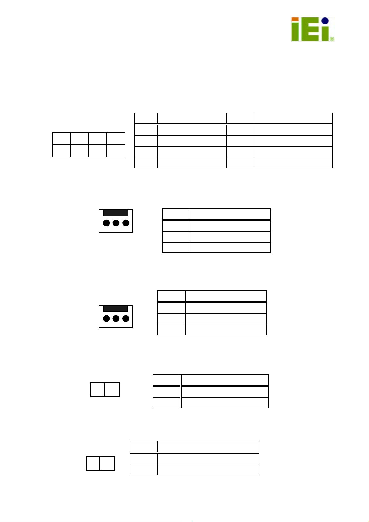
1. USB1, USB2: External 4 Port USB Connectors From the Mainboard
7 5 3 1
● ● ● ■
● ● ● ●
2. FAN1, FAN2, FAN3, FAN4: Fan Connector
3. ATXCTL1: Backplane to Mainboard ATX Power Control
Connector
PIN DESCRIPTION PIN DESCRIPTION
1 USBVCC 2 GND
3 DATA- 4 DATA+
5 DATA+ 6 DATA7 GND 8 USBVCC
PIN DESCRIPTION
1 GND
123
2 +12V
3 NC
PIN DESCRIPTION
1 GND
2 PSON#
4. PWRBTN: External Power On Button
■ ●
1 2
■ ●
1 2
5. RESET: Reset Button Connector
123
PIN DESCRIPTION
1 GND
2 SHB_RST#
3 5VSB
PIN DESCRIPTION
1 PWRBT#
2 GND
1
Page 2
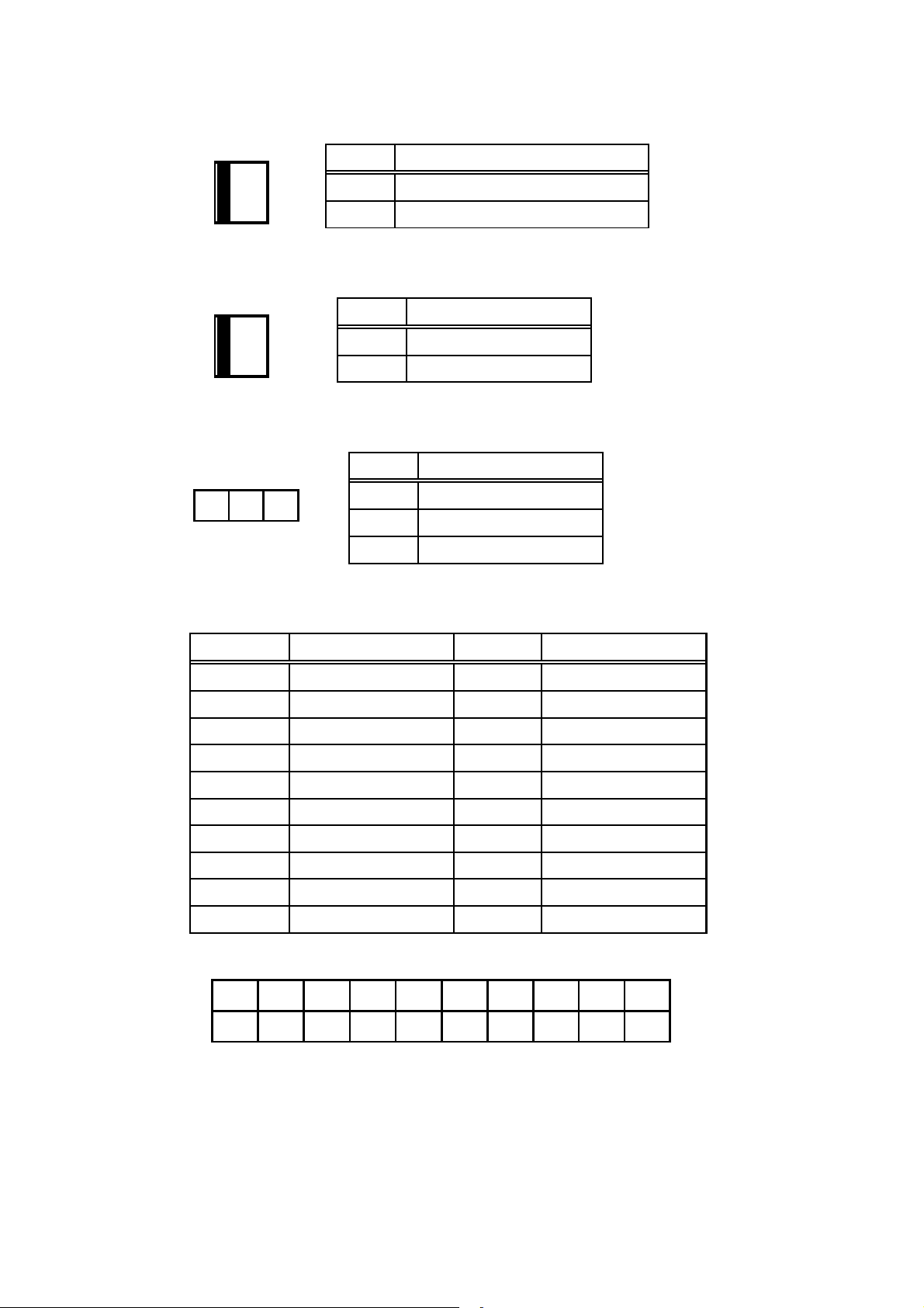
6. PWRGD: External Power Good Connector
2
1
●
■
PIN DESCRIPTION
1 GND
2 PWRGD
7. SM-BUS: External System Management BUS Connector
●
■
2
1
PIN DESCRIPTION
1 SMDATA
2 SMBCLK
8. CN1: PCIE X16 SDVO Control Signal Pin
1 2 3
■ ● ●
PIN DESCRIPTION
1 EXP_EN
2 SDVO_CLK
3 SDVO_DAT
9. IOPWR: The I/O Power Connector indicators for controlling your
CPU board
PIN DESCRIPTION PIN DESCRIPTION
1 GND 2 -12V
3 +12V 4 GND
5 IPMB_DA 6 5VSB
7 GND 8 GND
9 IPMB_CL 10 5VSB
11 +5V 12 PWRGD
13 SMDATA 14 SHB_RST#
15 5VSB 16 GND
17 SMBCLK 18 PSON#
19 +3.3V 20 PWRBT#
19 17 15 13 11 9 7 5 3 1
● ● ● ● ● ● ● ● ● ■
● ● ● ● ● ● ● ● ● ●
20 18 16 14 12 10
8642
2
Page 3

10. PWR2, PWR3: AT +5V Power Connector
1
2
3
■
●
●
PIN DESCRIPTION
1 +5V
2 +5V
3 +5V
●
4
4 GND
●
●
5 GND
6GND
5
6
11. J1, J2, J3: Write Protect Setup
J1、J2 and J3 are the EEPROM write protect pin of the PCI Express to
PCI Bridge will allow EEPROM normal read/write operations when J1、
J2 or J3 held high. When the Jump is brought low and the EEPROM
WPEN bit is “1”, all write operations to the status register are inhibited.
1 2
■ ●
J1、J2、J3
ON (Low) Write Inhibited
OFF (High)
DESCRIPTION
Normal Read/Wr i t e
(default)
12. PCI routing table:
13. Notice:
a. Recommend to use 6mm width spacer to install
b. Torsion must less than 6lb-inch
3
Page 4

14. Dimension:
4
 Loading...