

Page 1
NANO-PV-D4252/N4552/D5252 EPIC SBC
IEI Technology Corp.
MODEL:
NANO-PV-D4252/N4552/D5252
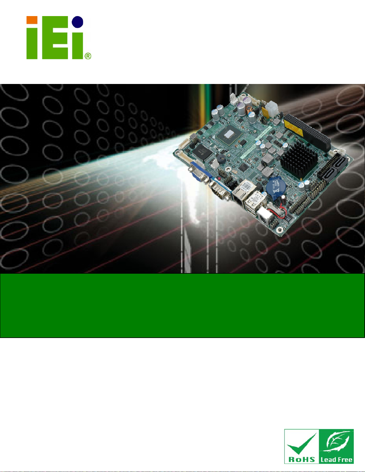
EPIC Motherboard with Intel® Atom™ processor
D425/N455/D525, VGA, Dual LVDS, GbE LAN, Eight USB 2.0,
Two SATA 3Gb/s, Four RS-232, RS-232/422/485, PCIe mini,
PCI-104, RoHS
User Manual
Rev. 1.05 – 31 December, 2011
Page i
Page 2
NANO-PV-D4252/N4552/D5252 EPIC SBC
Revision
Date Version Changes
31 December, 2011 1.05 Added note to Section 3.1.3 and Section 4.8
24 August, 2011 1.04 Minor revision to pin definitions in the following sections:
4.5.9 LVDS1 Screen Resolution Selection
4.5.10 LVDS2 Screen Resolution Selection
17 June, 2011 1.03 Minor revision to pin definitions in section 3.2.16 Power
Connector
18 April, 2011 1.02 Updated Table 4-7, 4-8, and 4-10 jumper settings.
Updated KEY1 connector to LVDS2 Backlight Adjustment.
6 January, 2011 1.01 Revised Pins 11, 12, 23, 24 in Table 3-14 LVDS2
Connector Pinouts
24 November, 2010 1.00 Initial release
Page ii
Page 3

NANO-PV-D4252/N4552/D5252 EPIC SBC
COPYRIGHT NOTICE
The information in this document is subject to change without prior notice in order to
improve reliability, design and function and does not represent a commitment on the part
of the manufacturer.
In no event will the manufacturer be liable for direct, indirect, special, incidental, or
consequential damages arising out of the use or inability to use the product or
documentation, even if advised of the possibility of such damages.
This document contains proprietary information protected by copyright. All rights are
Copyright
reserved. No part of this manual may be reproduced by any mechanical, electronic, or
other means in any form without prior written permission of the manufacturer.
TRADEMARKS
All registered trademarks and product names mentioned herein are used for identification
purposes only and may be trademarks and/or registered trademarks of their respective
owners.
Page iii
Page 4

NANO-PV-D4252/N4552/D5252 EPIC SBC
Table of Contents
1 INTRODUCTION.......................................................................................................... 1
1.1 INTRODUCTION........................................................................................................... 2
1.2 CONNECTORS ............................................................................................................. 3
1.3 DIMENSIONS............................................................................................................... 4
1.4 DATA FLOW................................................................................................................ 5
1.5 TECHNICAL SPECIFICATIONS ...................................................................................... 6
2 UNPACKING................................................................................................................. 8
2.1 ANTI-STATIC PRECAUTIONS........................................................................................ 9
2.2 UNPACKING PRECAUTIONS......................................................................................... 9
2.3 PACKING LIST........................................................................................................... 10
2.3.1 Optional Items...................................................................................................11
3 CONNECTORS ........................................................................................................... 12
3.1 PERIPHERAL INTERFACE CONNECTORS..................................................................... 13
3.1.1 NANO-PV-D4252/N4552/D5252 Layout......................................................... 13
3.1.2 Peripheral Interface Connectors ..................................................................... 14
3.1.3 External Interface Panel Connectors............................................................... 15
3.2 INTERNAL PERIPHERAL CONNECTORS...................................................................... 16
3.2.1 Audio Connector .............................................................................................. 16
3.2.2 Battery Connector............................................................................................ 16
3.2.3 CompactFlash® Slot........................................................................................ 17
3.2.4 Digital I/O Connector...................................................................................... 18
3.2.5 Fan Connector (CPU)...................................................................................... 19
3.2.6 Fan Connector (System) .................................................................................. 20
3.2.7 Front Panel Connector.................................................................................... 20
3.2.8 Keyboard/Mouse Connector............................................................................ 21
3.2.9 Backlight Inverter Connector .......................................................................... 22
3.2.10 LVDS Backlight Adjustment (LVDS2)............................................................ 23
3.2.11 LVDS1 LCD Connector.................................................................................. 23
3.2.12 LVDS2 LCD Connector ................................................................................. 24
Page iv
Page 5

NANO-PV-D4252/N4552/D5252 EPIC SBC
3.2.13 Parallel Port Connector ................................................................................ 25
3.2.14 PCI-104 Connector........................................................................................ 26
3.2.15 PCIe Mini Card Slot ...................................................................................... 28
3.2.16 Power Connector (+12 V, power supply)....................................................... 29
3.2.17 SATA Drive Connectors ................................................................................. 30
3.2.18 SATA Power Connector.................................................................................. 31
3.2.19 Serial Port Connectors (RS-232)................................................................... 31
3.2.20 Serial Port Connector (RS-232/422/485) ...................................................... 33
3.2.21 SMBus Connector .......................................................................................... 33
3.2.22 SPI Flash Connector...................................................................................... 34
3.2.23 USB Connectors............................................................................................. 35
3.3 EXTERNAL PERIPHERAL INTERFACE CONNECTOR PANEL ......................................... 36
3.3.1 Ethernet Connector.......................................................................................... 36
3.3.2 Keyboard/Mouse Connector............................................................................ 37
3.3.3 USB Connectors............................................................................................... 38
3.3.4 VGA Connector................................................................................................ 38
4 INSTALLATION ......................................................................................................... 40
4.1 ANTI-STATIC PRECAUTIONS...................................................................................... 41
4.2 INSTALLATION CONSIDERATIONS.............................................................................. 42
4.2.1 Installation Notices.......................................................................................... 42
4.3 UNPACKING.............................................................................................................. 43
4.4 SO-DIMM INSTALLATION ....................................................................................... 43
4.4.1 SO-DIMM Installation..................................................................................... 44
JUMPER SETTINGS .................................................................................................... 44
4.5
4.5.1 AT Auto Button Power Select Jumper Settings ................................................ 45
4.5.2 AT /ATX Power Select Jumper Settings............................................................ 46
4.5.3 Clear CMOS Jumper........................................................................................ 47
4.5.4 COM 3 Function Select Jumper....................................................................... 48
4.5.5 COM 3 RS-422/485 Function Select Jumper................................................... 49
4.5.6 COM 3 RS-422/485 Termination Select Jumpers ............................................ 50
4.5.7 CompactFlash® Card Setup............................................................................ 51
4.5.8 CompactFlash® Voltage Selection .................................................................. 52
4.5.9 LVDS1 Screen Resolution Selection................................................................. 52
4.5.10 LVDS2 Screen Resolution Selection............................................................... 53
Page v
Page 6

NANO-PV-D4252/N4552/D5252 EPIC SBC
4.5.11 LVDS Voltage Selection.................................................................................. 54
4.5.12 PCI-104 Voltage Setup................................................................................... 55
CHASSIS INSTALLATION............................................................................................ 56
4.6
4.6.1 Airflow.............................................................................................................. 56
4.6.2 Motherboard Installation................................................................................. 56
4.7 INTERNAL PERIPHERAL DEVICE CONNECTIONS........................................................ 56
4.7.1 AT/ATX Power Connection.............................................................................. 56
4.7.2 Audio Kit Installation....................................................................................... 58
4.7.3 Single RS-232 Cable (w/o Bracket) ................................................................. 59
4.8 EXTERNAL PERIPHERAL INTERFACE CONNECTION ................................................... 60
4.8.1 LAN Connection (Single Connector)............................................................... 61
4.8.2 PS/2 Y-Cable Connection................................................................................. 62
4.8.3 Serial Device Connection ................................................................................ 63
4.8.4 USB Connection (Dual Connector)................................................................. 64
4.8.5 VGA Monitor Connection ................................................................................ 65
4.9
SOFTWARE INSTALLATION ........................................................................................ 66
5 BIOS SCREENS........................................................................................................... 69
5.1 INTRODUCTION......................................................................................................... 70
5.1.1 Starting Setup................................................................................................... 70
5.1.2 Using Setup...................................................................................................... 70
5.1.3 Getting Help..................................................................................................... 71
5.1.4 Unable to Reboot After Configuration Changes.............................................. 71
5.1.5 BIOS Menu Bar................................................................................................ 71
MAIN........................................................................................................................ 72
5.2
5.3 ADVANCED............................................................................................................... 73
5.3.1 ACPI Settings................................................................................................... 73
5.3.2 T rusted Computing........................................................................................... 74
5.3.3 CPU Configuration.......................................................................................... 75
5.3.4 SATA Configuration ......................................................................................... 77
5.3.5 USB Configuration........................................................................................... 78
5.3.6 Super IO Configuration ................................................................................... 79
5.3.6.1 Serial Port n Configuration....................................................................... 80
5.3.6.2 IrDA Configuration................................................................................... 83
5.3.6.3 Parallel Port Configuration....................................................................... 84
Page vi
Page 7

NANO-PV-D4252/N4552/D5252 EPIC SBC
5.3.7 H/W Monitor.................................................................................................... 85
5.3.8 Serial Port Console Redirection...................................................................... 87
CHIPSET ................................................................................................................... 88
5.4
5.4.1 Host Bridge Configuration .............................................................................. 89
5.4.1.1 OnChip VGA Configuration..................................................................... 90
5.4.2 South Bridge Configuration............................................................................. 91
5.4.3 Intel IGD SWSCI OpRegion............................................................................. 92
5.5 BOOT........................................................................................................................ 94
5.6 SECURITY................................................................................................................. 95
5.7 EXIT......................................................................................................................... 97
A BIOS MENU OPTIONS............................................................................................. 99
B ONE KEY RECOVERY........................................................................................... 101
B.1
ONE KEY RECOVERY INTRODUCTION.................................................................... 102
B.1.1 System Requirement....................................................................................... 102
B.1.2 Supported Operating System......................................................................... 102
B.2 SETUP PROCEDURE FOR WINDOWS........................................................................ 104
B.2.1 Hardware and BIOS Setup ............................................................................ 105
B.2.2 Create Partitions........................................................................................... 105
B.2.3 Install Operating System, Drivers and Applications..................................... 108
B.2.4 Build-up Recovery Partition.......................................................................... 108
B.2.5 Create Factory Default Image........................................................................110
B.3 SETUP PROCEDURE FOR LINUX...............................................................................115
RECOVERY TOOL FUNCTIONS .................................................................................118
B.4
B.4.1 Factory Restore............................................................................................. 120
B.4.2 Backup System............................................................................................... 121
B.4.3 Restore Your Last Backup.............................................................................. 122
B.4.4 Manual........................................................................................................... 123
C TERMINOLOGY ..................................................................................................... 124
D WATCHDOG TIMER .............................................................................................. 128
E HAZARDOUS MATERIALS DISCLOSURE ....................................................... 131
E.1 HAZARDOUS MATERIAL DISCLOSURE TABLE FOR IPB PRODUCTS CER TIFIED AS
ROHS COMPLIANT UNDER 2002/95/EC WITHOUT MERCURY..................................... 132
Page vii
Page 8

NANO-PV-D4252/N4552/D5252 EPIC SBC
List of Figures
Figure 1-1: NANO-PV-D4252/N4552/D5252 ..................................................................................2
Figure 1-2: Connectors ..................................................................................................................3
Figure 1-3: NANO-PV-D4252/N4552/D5252 Dimensions (mm)...................................................4
Figure 1-4: Data Flow Block Diagram...........................................................................................5
Figure 3-1: Connector and Jumper Locations...........................................................................13
Figure 3-2: Audio Connector Location.......................................................................................16
Figure 3-3: Battery Connector Location.....................................................................................17
Figure 3-4: CompactFlash® Slot Location.................................................................................17
Figure 3-5: Digital I/O Connector Locations ..............................................................................19
Figure 3-6: CPU Fan Connector Location..................................................................................19
Figure 3-7: +12V Fan Connector Locations...............................................................................20
Figure 3-8: Front Panel Connector Location .............................................................................21
Figure 3-9: Keyboard/Mouse Connector Location....................................................................22
Figure 3-10: Backlight Inverter Connector Location.................................................................22
Figure 3-11: LPC Connector Location........................................................................................23
Figure 3-12: LVDS1 Connector Locations .................................................................................24
Figure 3-13: LVDS2 Connector Location ...................................................................................25
Figure 3-14: Parallel Port Connector Location..........................................................................26
Figure 3-15: PCI-104 Connector Location..................................................................................27
Figure 3-16: PCIe Mini Card Slot Location.................................................................................28
Figure 3-17: CPU 12V Power Connector Location....................................................................30
Figure 3-18: SATA Drive Connector Locations.........................................................................30
Figure 3-19: SATA Power Connector Locations .......................................................................31
Figure 3-20: COM Connector Pinout Locations ........................................................................32
Figure 3-21: Serial Port Connector Location.............................................................................33
Figure 3-22: SMBus Connector Locations.................................................................................34
Figure 3-23: SPI Flash Connector...............................................................................................34
Figure 3-24: USB Connector Pinout Locations.........................................................................35
Figure 3-25: NANO-PV-D4252/N4552/D5252 External Peripheral Interface Connector.........36
Figure 3-26: RJ-45 Ethernet Connector......................................................................................37
Page viii
Page 9

NANO-PV-D4252/N4552/D5252 EPIC SBC
Figure 3-27: PS/2 Pinout and Configuration..............................................................................37
Figure 3-28: VGA Connector .......................................................................................................39
Figure 4-1: SO-DIMM Installation................................................................................................44
Figure 4-2: AT Auto Button Select Jumper Settings.................................................................46
Figure 4-3: AT/ATX Power Select Jumper Location..................................................................47
Figure 4-4: Clear CMOS Jumper .................................................................................................48
Figure 4-5: COM 3 Function Select Jumper Location...............................................................49
Figure 4-6: COM 3 RS-422/485 Function Select Jumper Location ..........................................50
Figure 4-7: COM 3 RS-422 and RS-485 Termination Select Jumper Location .......................51
Figure 4-8: CompactFlash® Setup Jumper Location ...............................................................51
Figure 4-9: CompactFlash® Voltage Selection Jumper Location ...........................................52
Figure 4-10: LVDS1 Screen Resolution Jumper Location........................................................53
Figure 4-11: LVDS2 Screen Resolution Jumper Location........................................................54
Figure 4-12: LVDS Voltage Selection Jumper Locations .........................................................55
Figure 4-13: PCI-104 Voltage Jumper Location.........................................................................55
Figure 4-14: Power Cable to Motherboard Connection............................................................57
Figure 4-15: Connect Power Cable to Power Supply................................................................58
Figure 4-16: Audio Kit Cable Connection ..................................................................................59
Figure 4-17: Single RS-232 Cable Installation ...........................................................................60
Figure 4-18: LAN Connection......................................................................................................62
Figure 4-19: PS/2 Keyboard/Mouse Connector.........................................................................63
Figure 4-20: Serial Device Connector.........................................................................................64
Figure 4-21: USB Connector........................................................................................................65
Figure 4-22: VGA Connector .......................................................................................................66
Figure 4-23: Introduction Screen................................................................................................67
Figure 4-24: Available Drivers.....................................................................................................68
Figure B-1: Recovery Tool Setup Menu .................................................................................. 106
Figure B-2: Command Mode..................................................................................................... 106
Figure B-3: Partition Creation Commands.............................................................................. 107
Figure B-4: System Configuration for Windows .................................................................... 109
Figure B-5: Build-up Recovery Partition................................................................................. 109
Figure B-6: Press any key to continue.................................................................................... 110
Figure B-7: Press F3 to Boot into Recovery Mode................................................................. 110
Figure B-8: Recovery Tool Menu ............................................................................................. 111
Figure B-9: About Symantec Ghost Window.......................................................................... 111
Page ix
Page 10

Figure B-10: Symantec Ghost Path ......................................................................................... 112
Figure B-11: Select a Local Source Drive ............................................................................... 112
Figure B-12: Select a Source Partition from Basic Drive ...................................................... 112
Figure B-13: File Name to Copy Image to ............................................................................... 113
Figure B-14: Compress Image.................................................................................................. 114
Figure B-15: Image Creation Confirmation............................................................................. 114
Figure B-16: Image Creation Complete................................................................................... 114
Figure B-17: Image Creation Complete................................................................................... 115
Figure B-18: Press Any Key to Continue................................................................................ 115
Figure B-19: Partitions for Linux.............................................................................................. 116
Figure B-20: System Configuration for Linux......................................................................... 117
Figure B-21: Access menu.lst in Linux (Text Mode).............................................................. 117
Figure B-22: Recovery Tool Menu ........................................................................................... 118
Figure B-23: Recovery Tool Main Menu.................................................................................. 119
NANO-PV-D4252/N4552/D5252 EPIC SBC
Figure B-24: Restore Factory Default...................................................................................... 120
Figure B-25: Recovery Complete Window.............................................................................. 120
Figure B-26: Backup System.................................................................................................... 121
Figure B-27: System Backup Complete Window ................................................................... 121
Figure B-28: Restore Backup................................................................................................... 122
Figure B-29: Restore System Backup Complete Window..................................................... 122
Figure B-30: Symantec Ghost Window ................................................................................... 123
Page x
Page 11

NANO-PV-D4252/N4552/D5252 EPIC SBC
List of Tables
Table 1-1: Technical Specifications..............................................................................................7
Table 3-1: Peripheral Interface Connectors...............................................................................15
Table 3-2: Rear Panel Connectors..............................................................................................15
Table 3-3: Audio Connector Pinouts ..........................................................................................16
Table 3-4: Battery Connector Pinouts........................................................................................17
Table 3-5: CompactFlash® Slot Pinouts....................................................................................18
Table 3-6: Digital I/O Connector Pinouts....................................................................................19
Table 3-7: CPU Fan Connector Pinouts......................................................................................20
Table 3-8: +12V Fan Connector Pinouts.....................................................................................20
Table 3-9: Front Panel Connector Pinouts.................................................................................21
Table 3-10: Keyboard/Mouse Connector Pinouts .....................................................................22
Table 3-11: Backlight Inverter Connector Pinouts....................................................................23
Table 3-12: LPC Connector Pinouts ...........................................................................................23
Table 3-13: LVDS1 Connector Pinouts.......................................................................................24
Table 3-14: LVDS2 Connector Pinouts.......................................................................................25
Table 3-15: Parallel Port Connector Pinouts................................................................26
Table 3-16: PCI-104 Connector Pinouts .....................................................................................28
Table 3-17: PCIe Mini Card Slot Pinouts ....................................................................................29
Table 3-18: CPU 12V Power Connector Pinouts........................................................................30
Table 3-19: SATA Drive Connector Pinouts...............................................................................31
Table 3-20: SATA Power Connector Pinouts.............................................................................31
Table 3-21: COM Connector Pinouts..........................................................................................32
Table 3-22: Serial Port Connector Pinouts ................................................................................33
Table 3-23: SMBus Connector Pinouts ......................................................................................34
Table 3-24: SPI Flash Connector Pinouts ..................................................................................35
Table 3-25: USB Port Connector Pinouts...................................................................................35
Table 3-26: LAN Pinouts ..............................................................................................................37
Table 3-27: RJ-45 Ethernet Connector LEDs.............................................................................37
Table 3-28: Keyboard Connector Pinouts..................................................................................38
Table 3-29: USB Port Connector Pinouts...................................................................................38
Page xi
Page 12

Table 3-30: VGA Connector Pinouts...........................................................................................39
Table 4-1: Jumpers.......................................................................................................................45
Table 4-2: AT Auto Button Power Select Jumper Settings ......................................................46
Table 4-3: AT/ATX Power Select Jumper Settings....................................................................46
Table 4-4: Clear CMOS Jumper Settings....................................................................................48
Table 4-5: COM 3 Function Select Jumper Settings.................................................................48
Table 4-6: COM 3 RS-422/485 Function Select Jumper Settings.............................................49
Table 4-7: COM 3 RS-422 Termination Select Jumper Settings ..............................................50
Table 4-8: COM 3 RS-485 Termination Select Jumper Settings ..............................................50
Table 4-9: CompactFlash® Setup Jumper Settings..................................................................51
Table 4-10: CompactFlash® Voltage Selection Jumper Settings............................................52
Table 4-11: LVDS1 Screen Resolution Jumper Settings..........................................................53
Table 4-12: LVDS2 Screen Resolution Jumper Settings..........................................................54
Table 4-13: LVDS Voltage Selection Jumper Settings..............................................................54
NANO-PV-D4252/N4552/D5252 EPIC SBC
Table 4-14: PCI-104 Voltage Jumper Settings...........................................................................55
Table 5-1: BIOS Navigation Keys................................................................................................71
Page xii
Page 13
NANO-PV-D4252/N4552/D5252 EPIC SBC
BIOS Menus
BIOS Menu 1: Main.......................................................................................................................72
BIOS Menu 2: Advanced..............................................................................................................73
BIOS Menu 3: ACPI Settings .......................................................................................................74
BIOS Menu 4: TPM Configuration...............................................................................................75
BIOS Menu 5: CPU Configuration...............................................................................................76
BIOS Menu 6: IDE Configuration.................................................................................................77
BIOS Menu 7: USB Configuration...............................................................................................78
BIOS Menu 8: Super IO Configuration........................................................................................79
BIOS Menu 9: Serial Port n Configuration Menu.......................................................................80
BIOS Menu 10: IrDA Configuration Menu...................................................................................83
BIOS Menu 11: Parallel Port Configuration Menu.....................................................................84
BIOS Menu 12: Hardware Health Configuration........................................................................86
BIOS Menu 13: Serial Port Console Redirection.......................................................................87
BIOS Menu 14: Chipset................................................................................................................88
BIOS Menu 15: Host Bridge Chipset Configuration..................................................................89
BIOS Menu 16: OnChip VGA Configuration...............................................................................90
BIOS Menu 17:South Bridge Chipset Configuration.................................................................91
BIOS Menu 18:South Bridge Chipset Configuration.................................................................92
BIOS Menu 19: Boot.....................................................................................................................94
BIOS Menu 20: Security...............................................................................................................96
BIOS Menu 21:Exit........................................................................................................................97
Page xiii
Page 14

NANO-PV-D4252/N4552/D5252 EPIC SBC
Page xiv
Page 15
NANO-PV-D4252/N4552/D5252 EPIC SBC
1 Introduction
Chapter
1
Page 1
Page 16
1.1 Introduction
NANO-PV-D4252/N4552/D5252 EPIC SBC
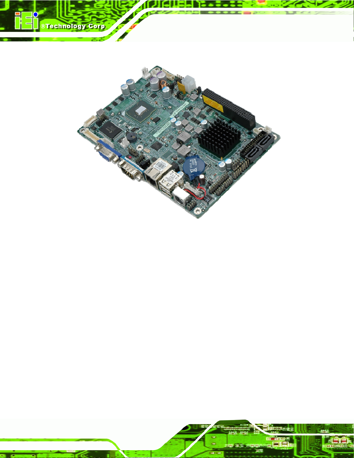
Figure 1-1: NANO-PV-D4252/N4552/D5252
The NANO-PV-D4252/N4552/D5252 EPIC motherboard is a Intel® Atom™ processor
D525, D425 or N455 platform. Up to one 2.0 GB 800 MHz or 667 MHz DDR3 SDRAM
SO-DIMM is supported by the NANO-PV-D4252/N4552/D5252.
The integrated Intel® ICH8M Chipset supports a GbE LAN port through the Realtek
RTL8111E Ethernet controller (with ASF 2.0 support). The
NANO-PV-D4252/N4552/D5252 also supports two SATA 3Gb/s drives and provides 5 V
SATA power.
The NANO-PV-D4252/N4552/D5252 supports dual display via VGA and two internal
LVDS LCD connectors. Eight USB 2.0 channels, one PCIe mini socket, one PCI-104 slot
and internal one parallel port connector provide flexible expansion options. High Definition
Audio (HDA) support ensures HDA devices can be easily implemented on the
NANO-PV-D4252/N4552/D5252. Serial device connectivity is provided by a RS-232 seri al
Page 2
port, three internal RS-232 and one internal RS-232/422/485 connectors.
Page 17
NANO-PV-D4252/N4552/D5252 EPIC SBC
1.2 Connectors
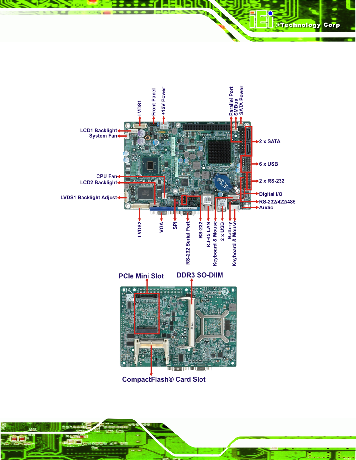
The connectors on the NANO-PV-D4252/N4552/D5252 are sho wn in the figure below.
Figure 1-2: Connectors
Page 3
Page 18
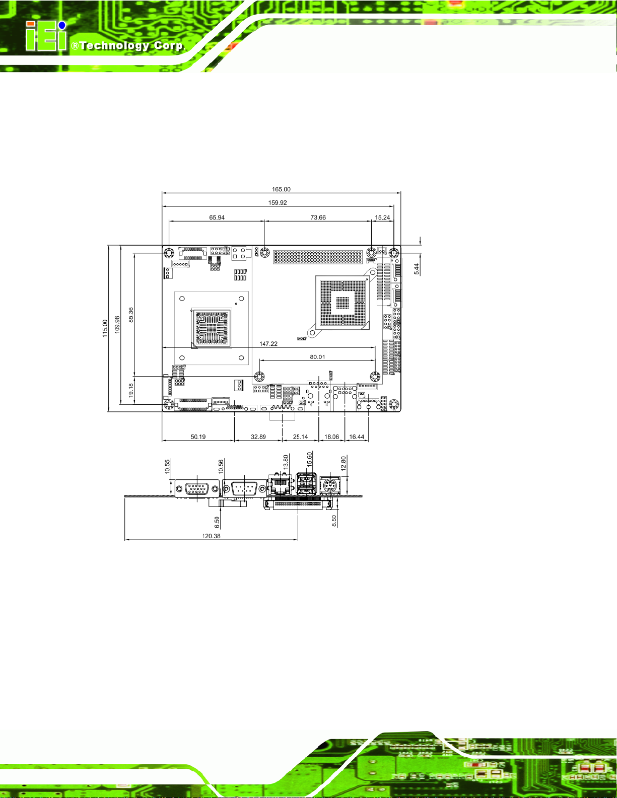
1.3 Dimensions
The dimensions of the board are listed below:
Length: 165 mm
Width: 115 mm
NANO-PV-D4252/N4552/D5252 EPIC SBC
Figure 1-3: NANO-PV-D4252/N4552/D5252 Dimensions (mm)
Page 4
Page 19
NANO-PV-D4252/N4552/D5252 EPIC SBC
1.4 Data Flow
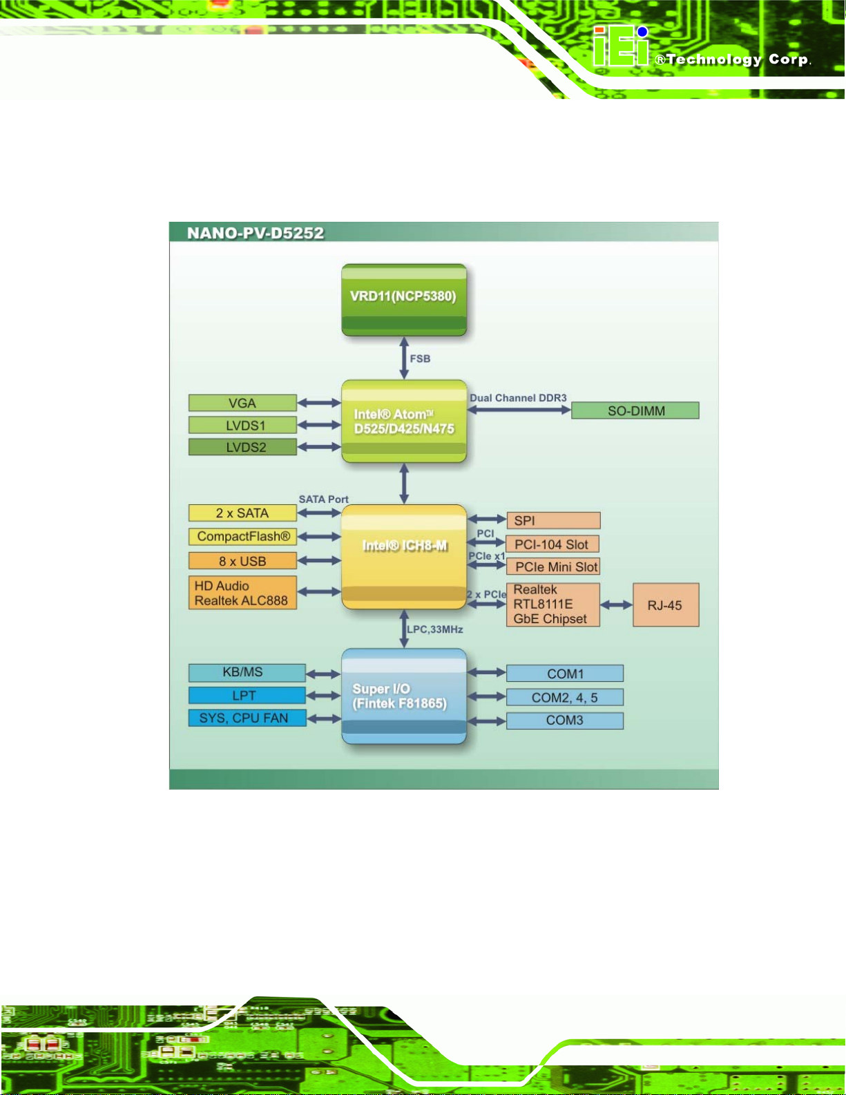
6Figure 1-4 shows the data flow between the two on-board chipsets and other components
installed on the motherboard and described in the following sections of this chapter.
Figure 1-4: Data Flow Block Diagram
Page 5
Page 20
NANO-PV-D4252/N4552/D5252 EPIC SBC
1.5 Technical Specifications
NANO-PV-D4252/N4552/D5252 technical specifications are listed in table belo w.
Specification NANO-PV-D4252/N4552/D5252
Form Factor
CPU options
Express Chipset
Memory
Audio
LAN
Super I/O
Digital I/O
BIOS
Watchdog Timer
EPIC
Intel® Atom™ processor D525, 1.8 GHz/1 MB L2 cache
Intel® Atom™ processor D425, 1.8 GHz/512 KB L2 cache
Intel® Atom™ processor N455, 1.66 GHz/512 KB L2 cache
Intel® ICH8M
One 204-pin SO-DIMM sockets support one 800/6 67 MHz
2.0 GB (max.) DDR3 SDRAM SO-DIMM (system max. 2 GB)
Realtek ALC888 HD 7.1 channel audio codec
One Realtek RTL8111E PCIe GbE controller with ASF 2.0
support
Fintek F81865
8-bit, 4-bit input/4-bit output
AMI BIOS label
Software programmable supports 1~2 55 sec. system reset
Expansion
PCIe
PCI
I/O Interface Connectors
Audio Connector
Display Ports
Ethernet
Page 6
One PCIe Mini slot
One PCI-104 slot
One internal audio connector (10-pin header)
One VGA port (2048x1536)
One internal 18/24bit single/dual-channel LVDS connector (up
to 1920 x 1080)
One internal 18-bit single-channel LVDS connector (up to
1024 x 768 or 1366 x 768)
One RJ-45 GbE ports
Page 21
NANO-PV-D4252/N4552/D5252 EPIC SBC
Specification NANO-PV-D4252/N4552/D5252
Serial Ports
USB 2.0/1.1 Ports
Parallel Ports
Storage
Serial ATA
CompactFlash®
Environmental and Power Specifications
Power Supply
Power Connector
One RS-232 serial port
Three RS-232 via four 10-pin headers
One RS-232/422/485 via 14–pin header
Two external USB ports
Six internal USB ports via three 8-pin headers
One LPT connector via 26-pin header
Two SATA 3.0 Gb/s connectors with RAID 0,1 support
One 5 V SATA power connector
One CompactFlash® Type II socket
12 V only
ATX and AT power supported
One internal 4-pin Molex power connector for power supply
Power Consumption
Operating Temperature
Humidity
Physical Specifications
Dimensions
Weight GW/NW
Table 1-1: Technical Specifications
12V@2.21A( Intel® Atom™ D525 with 1GB 667Mhz DDR3)
-10ºC ~ 60ºC (requires cooler and silicone heat sink paste)
5% ~ 95% (non-condensing)
165 mm x 115 mm
850 g / 350 g
Page 7
Page 22
NANO-PV-D4252/N4552/D5252 EPIC SBC
Chapter
2
2 Unpacking
Page 8
Page 23
NANO-PV-D4252/N4552/D5252 EPIC SBC
2.1 Anti-static Precautions
WARNING!
Static electricity can destroy certain electronics. Make sure to follow the
ESD precautions to prevent damage to the product, and injury to the
user.
Make sure to adhere to the following guidelines:
Wear an anti-static wristband: Wearing an anti-static wristband can prevent
electrostatic discharge.
Self-grounding: Touch a g rounded cond uctor every few minutes to discharge
any excess static buildup.
Use an anti-static pad: When configuring any circuit board, place it on an
anti-static mat.
Only handle the edges of the PCB: Don't touch the surface of the
motherboard. Hold the motherboard by the edges when handling.
2.2 Unpacking Precautions
When the NANO-PV-D4252/N4552/D5252 is unpacked, please do the following:
Follow the antistatic guidelines above.
Make sure the packing box is facing upwards when opening.
Make sure all the packing list items are present.
Page 9
Page 24
2.3 Packing List
NOTE:
If any of the components listed in the checklist below are missing, do
not proceed with the installation. Contact the IEI reseller or vendor the
NANO-PV-D4252/N4552/D5252 was purchased from or contact an IEI
NANO-PV-D4252/N4552/D5252 EPIC SBC
sales representative directly by sending an email to
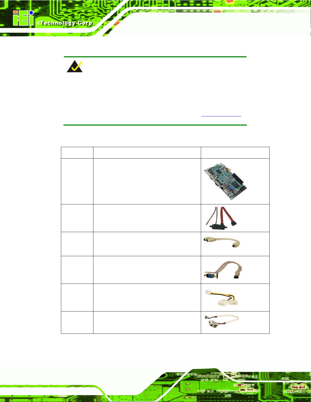
The NANO-PV-D4252/N4552/D5252 is shipped with the following components:
Quantity Item and Part Number Image
1 NANO-PV-D4252/N4552/D5252-R10, or
NANO-PV- D4252-R10, or
NANO-PV- N4552-R10 motherboard
1 SATA and 5 V power cable
(P/N: 32000-114000-RS)
1 KB/MS PS/2 Y-cable
(P/N: 32000-000138-RS)
32sales@iei.com.tw.
Page 10
2 RS-232 serial port cable
(P/N: 32200-000049-RS)
1 AT 12 V Cable
(P/N: 32100-087100-RS)
1 Audio cable
(P/N: 32000-072100-RS)
Page 25
NANO-PV-D4252/N4552/D5252 EPIC SBC
1 Dual USB cable (w bracket)
(P/N:CB-USB02A-RS)
1 Mini jumper pack (2.0mm)
(P/N: 33100-000033-RS)
1 Utility CD
1 Quick Installation Guide
2.3.1 Optional Items
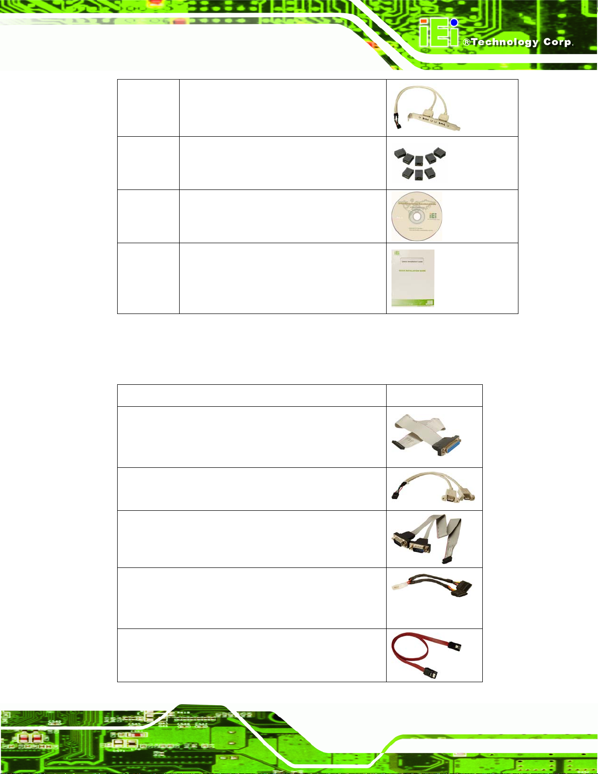
The following are optional components which may be separately purchased:
Item and Part Number Image
LPT cable (wo bracket)
(P/N: 32200-015100-RS)
Dual USB cable (wo bracket)
(P/N: 32000-044300-RS)
RS-232/422/485 cable
(P/N: 32200-026500-RS)
SATA power cable
(P/N: 32100-000100-100-RS)
(P/N: 32100-000100-200-RS)
SATA cable
(P/N: 32000-062800-RS)
Page 11
Page 26

NANO-PV-D4252/N4552/D5252 EPIC SBC
Chapter
3
3 Connectors
Page 12
Page 27
NANO-PV-D4252/N4552/D5252 EPIC SBC
3.1 Peripheral Interface Connectors
This chapter details all the jumpers and connectors.
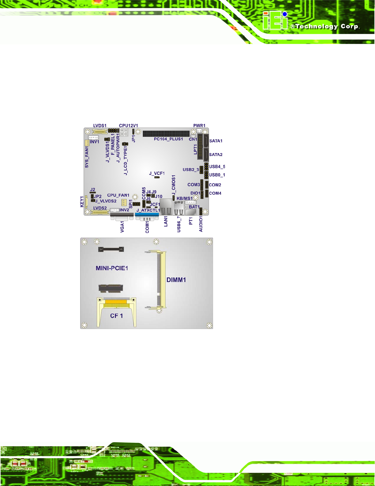
3.1.1 NANO-PV-D4252/N4552/D5252 Layout
The figures below show all the connectors and jumpers.
Figure 3-1: Connector and Jumper Locations
Page 13
Page 28
NANO-PV-D4252/N4552/D5252 EPIC SBC
3.1.2 Peripheral Interface Connectors
The table below lists all the connectors on the board.
Connector Type Label
Audio connector 10-pin header AUDIO1
Battery connector 2-pin wafer BAT1
BIOS update connector 6-pin wafer SPI1
CompactFlash® slot 50-pin header CF1
DDR3 SO-DIMM socket 204-pin socket DIMM1
Digital I/O connector 10-pin header DIO1
Fan connector (CPU) 3-pin wafer CPU_FAN1
Fan connector (system) 3-pin wafer SYS_FAN1
Front panel connector 8-pin header F_PANEL1
Keyboard and mouse connector 6-pin wafer KB/MS1
LVDS1 backlight inverter connector 5-pin wafer INV1
LVDS2 backlight inverter connector 5-pin wafer INV2
LVDS2 backlight adjust connector 9-pin wafer KEY1
LVDS1 LCD connector 30-pin crimp LVDS1
LVDS2 LCD connector 20-pin crimp LVDS2
Parallel port connector 26-pin header LPT1
PCI-104 connector PCI-104 connector PC104_PLUS1
PCIe Mini card slot PCIe Mini card slot MINI_PCIE1
Power connector (+12V, power supply) 4-pin connector CPU12V1
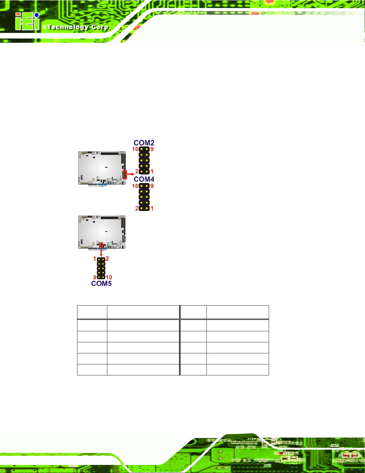
RS-232 serial port connector 10-pin header COM2
Page 14
RS-232 serial port connector 10-pin header COM4
RS-232 serial port connector 10-pin header COM5
RS-232/422/485 serial port connector 14-pin header COM3
Page 29
NANO-PV-D4252/N4552/D5252 EPIC SBC
Serial ATA (SATA) drive connector 7-pin SATA SATA1
Serial ATA (SATA) drive connector 7-pin SATA SATA2
SATA power con nector 2-pin wafe r PWR1
SMBus connector 4-pin wafe r CN1
USB connector 8-pin header USB0_1
USB connector 8-pin header USB2_3
USB connector 8-pin header USB4_5
Table 3-1: Peripheral Interface Connectors
3.1.3 External Interface Panel Connectors
NOTE:
Due to limited space on the mainboard, the VGA and COM port on the
I/O panel cannot be used simultaneously. To utilize both the VGA and
COM port at the same time, please connect the RS-232 COM port
cable to the mainboard pin-header. For convenience, the mainboard
provides support for a maximum of four COM ports plus one VGA port
or five COM ports without VGA setup.
The table below lists the connectors on the external I/O panel.
Connector Type Label
Ethernet connector RJ-45 LAN1
Keyboard/Mouse connector PS/2 PT1
VGA port connector 15-pin Female VGA1
Serial port (RS-232) connector 9-pin male COM1
USB ports (dual) USB port USB6_7
Table 3-2: Rear Panel Connectors
Page 15
Page 30
NANO-PV-D4252/N4552/D5252 EPIC SBC
3.2 Internal Peripheral Connectors
The section describes all of the connectors on the NANO-PV-D4252/N4552/D5252.
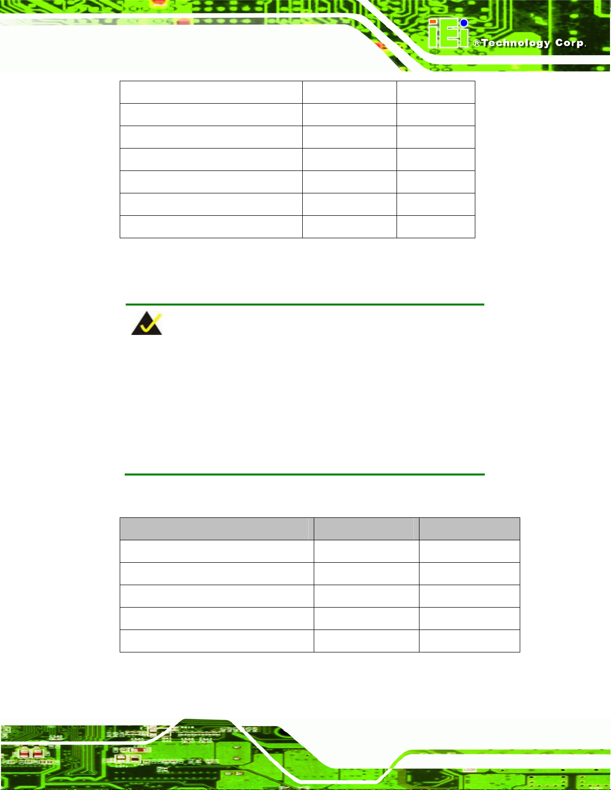
3.2.1 Audio Connector
CN Label: AUDIO1
CN Type:
CN Location:
CN Pinou
The audi
microphones for the input and output of audio signals to and from the system.
ts:
o connector is connected to external audio devices including speakers and
10-pin header (2x5)
See Figure 3-2
See Table 3-3
Figure 3-2: Audio Connector Location
PIN NO. DESCRIPTION PIN NO. DESCRIPTION
1 LFRONT-R 2 LLINE-R
3 GND 4 GND
5 LFRONT-L 6 LLINE-L
7 GND 8 GND
9 LMIC1-CONN-R 10 LMIC1-CONN-L
Table 3-3: Audio Connector Pinouts
3.2.2 Battery Connector
CN Label: BAT1
CN Type:
CN Location:
ts:
Page 16
CN Pinou
2-pin wafer (1x2)
See Figure 3-3
See Table 3-4
Page 31

NANO-PV-D4252/N4552/D5252 EPIC SBC
This is connected to the system battery. The battery provides power to the system clock to
retain the time when power is turned off.
Figure 3-3: Battery Connector Location
Pin Description
1 Battery+
2 Ground
Table 3-4: Battery Connector Pinouts
3.2.3 CompactFlash® Slot
CN Label: CF1
CN Type:
CN Location:
CN Pinou
A Compac
Figure 3-4: CompactFlash® Slot Location
ts:
tFlash® Type I/II card can be used in this slot.
CompactFlash® card slot
See Figure 3-4
See Table 3-5
Pin Description Pin Description
1 GROUND 26 VCC-IN CHECK1
Page 17
Page 32

Pin Description Pin Description
2 DATA 3 27 DATA 11
3 DATA 4 28 DATA 12
4 DATA 5 29 DATA 13
5 DATA 6 30 DATA 14
6 DATA 7 31 DATA 15
7 HDC_CS0# 32 HDC_CS1
8 GROUND 33 N/C
9 GROUND 34 IOR#
10 GROUND 35 IOW#
11 GROUND 36 VCC_CF
12 GROUND 37 IRQ14
13 VCC_CF 38 VCC_CF
14 GROUND 39 CSEL
NANO-PV-D4252/N4552/D5252 EPIC SBC
15 GROUND 40 N/C
16 GROUND 41 HDD_RESET
17 GROUND 42 IORDY
18 SA2 43 SDREQ
19 SA1 44 SDACK#
20 SA0 45 HDD_ACTIVE#
21 DATA 0 46 66DET
22 DATA 1 47 DATA 8
23 DATA 2 48 DATA 9
24 N/C 49 DATA 10
25 VCC-IN CHECK2 50 GROUND
Table 3-5: CompactFlash® Slot Pinouts
3.2.4 Digital I/O Connector
CN Label: DIO1
Page 18
CN Type:
CN Location:
CN Pinou
ts:
10-pin header
See Figure 3-5
See Table 3-6
Page 33

NANO-PV-D4252/N4552/D5252 EPIC SBC
The digital I/O connector provides programmable input and output for external devices.
The digital I/O provides 4-bit output and 4-bit input.
Figure 3-5: Digital I/O Connector Locations
Pin Description Pin Description
1 GND 2 +5V
3 Output 3 4 Output 2
5 Output 1 6 Output 0
7 Input 3 8 Input 2
9 Input 1 10 Input 0
Table 3-6: Digital I/O Connector Pinouts
3.2.5 Fan Connector (CPU)
CN Label: CPU_FAN1
CN Type:
CN Location:
CN Pinou
The fan conn
ts:
3-pin wafer (1x3)
See Figure 3-6
See Table 3-7
ector attaches to a CPU cooling fan.
Figure 3-6: CPU Fan Connector Location
Page 19
Page 34

Pin Description
1 FANIO1
2 POWER
3 GND
Table 3-7: CPU Fan Connector Pinouts
3.2.6 Fan Connector (System)
CN Label: SYS_FAN1
NANO-PV-D4252/N4552/D5252 EPIC SBC
CN Type:
CN Location:
CN Pinouts:
3-pin wafer (1x3)
6Figure 3-7
See
6Table 3-8
See
The cooling fan connector provides a 12V, 500mA current to the cooling fan. The
connector has a "rotation" pin to get rotation signals from fans and notify the system so the
system BIOS can recognize the fan speed. Please note that only specified fans can issue
the rotation signals.
Figure 3-7: +12V Fan Connector Locations
PIN NO. DESCRIPTION
1 FANIO2
2 +12V
3 GND
Table 3-8: +12V Fan Connector Pinouts
3.2.7 Front Panel Connector
CN Label: F_PANEL1
Page 20
Page 35

NANO-PV-D4252/N4552/D5252 EPIC SBC
CN Type:
CN Location:
CN Pinou
ts:
The front pa
8-pin header (2x4)
See Figure 3-8
See Table 3-9
nel connector connects to external switches and indicators to monitor and
controls the motherboard. These indicators and switches include:
Power button
Reset
Power LED
HDD LED
Figure 3-8: Front Panel Connector Location
FUNCTION PIN DESCRIPTION FUNCTION PIN DESCRIPTION
1 PWR_BTN+ 2 PWR LED Power Button
3 GND
5 SATA LED PWT 6 RESET SATA LED
7 SATA_LED#
Table 3-9: Front Panel Connector Pinouts
3.2.8 Keyboard/Mouse Connector
CN Label: KB/MS1
CN Type:
CN Location:
CN Pinou
ts:
6-pin wafer (1x6)
See Figure 3-9
See Table 3-10
Power LED
4 GND
Reset
8 GND
Page 21
Page 36

NANO-PV-D4252/N4552/D5252 EPIC SBC
The keyboard/mouse connector connects to a PS/2 Y-cable that can be connected to a
PS/2 keyboard and mouse.
Figure 3-9: Keyboard/Mouse Connector Location
Pin Description
1 +5 VCC
2 MS DATA
3 MS CLK
4 KB DATA
5 KB CLK
6 GROUND
Table 3-10: Keyboard/Mouse Connector Pinouts
3.2.9 Backlight Inverter Connector
CN Label: INV1, INV2
CN Type:
CN Location:
CN Pinou
The ba
ts:
cklight inverter connector provides power to an LCD panel.
5-pin wafer (1x5)
See Figure 3-10
See Table 3-11
Page 22
Figure 3-10: Backlight Inverter Connector Location
Page 37

NANO-PV-D4252/N4552/D5252 EPIC SBC
Pin Description
1 BL_ADJ
2 GROUND
3 +12 V
4 GROUND
5 BACKLIGHT ENABLE
Table 3-11: Backlight Inverter Connector Pinouts
3.2.10 LVDS Backlight Adjustment (LVDS2)
CN Label: KEY1
CN Type:
CN Location:
CN Pinou
ts:
Interfaces to the LPC interface o
9-pin header
See Figure 3-11
See Table 3-12
n the Southbridge.
Figure 3-11: LPC Connector Location
Pin Description Pin Description
1 LED-BL 2 N/A
3 LED-AM 4 menu/enter
5 DOWN 6 UP
7 auto/exit 8 POWER
9 GND
Table 3-12: LPC Connector Pinouts
3.2.11 LVDS1 LCD Connector
CN Label: LVDS1
Page 23
Page 38

NANO-PV-D4252/N4552/D5252 EPIC SBC
CN Type:
CN Location:
CN Pinou
ts:
The LVDS1
connector is for an LCD panel connected to the board.
20-pin crimp (2x10)
See Figure 3-12
See Table 3-14
Figure 3-12: LVDS1 Connector Locations
Pin Description Pin Description
1 GROUND 2 GROUND
3 LVDSA_DATA0+ 4 LVDSA_DATA05 LVDSA_DATA1+ 6 LVDSA_DATA17 LVDSA_DATA2+ 8 LVDSA_DATA29 LVDSA_CLK+ 10 LVDSA_CLK11 N/C 12 N/C
13 GROUND 14 GROUND
15 LDDC_DATA 16 LDDC_CLK
17 VCC_LCD 18 VCC_LCD
19 VCC_LCD 20 VCC_LCD
Table 3-13: LVDS1 Connector Pinouts
3.2.12 LVDS2 LCD Connector
CN Label: LVDS2
CN Type:
CN Location:
CN Pinou
ts:
30-pin crimp (2x15)
See Figure 3-13
See Table 3-13
Page 24
Page 39

NANO-PV-D4252/N4552/D5252 EPIC SBC
The LVDS2 connector is for an LCD panel connected to the board.
Figure 3-13: LVDS2 Connector Location
Pin Description Pin Description
1 GROUND 2 GROUND
3 LVDSA_Y0+ 4 LVDSA_Y05 LVDSA_Y1+ 6 LVDSA_Y17 LVDSA_Y2+ 8 LVDSA_Y29 LVDSA_CLK+ 10 LVDSA_CLK11 LVDSA_Y3+ 12 LVDSA_Y313 GROUND 14 GROUND
15 LVDSB_Y0+ 16 LVDSB_Y017 LVDSB_Y1+ 18 LVDSB_Y119 LVDSB_Y2+ 20 LVDSB_Y221 LVDSB_CLK+ 22 LVDSB_CLK23 LVDSB_Y3+ 24 LVDSB_Y325 GROUND 26 GROUND
27 VCC_LVDS 28 VCC_LVDS
29 VCC_LVDS 30 VCC_LVDS
Table 3-14: LVDS2 Connector Pinouts
3.2.13 Parallel Port Connector
CN Label: LPT1
CN Type:
CN Location:
CN Pinou
ts:
26-pin box header
See Figure 3-14
See Table 3-15
Page 25
Page 40

NANO-PV-D4252/N4552/D5252 EPIC SBC
The parallel port connector connects to a parallel port connector interface or some other
parallel port device such as a printer.
Figure 3-14: Parallel Port Connector Location
Pin Description Pin Description
1 STROBE# 2 AFD
3 PTD0 4 ERROR#
5 PTD1 6 INITIALIZE
7 PTD 2 8 SLIN
9 PTD3 10 GROUND
11 PTD 4 12 GROUND
13 PTD 5 14 GROUND
15 PTD 6 16 GROUND
17 PTD7 18 GROUND
19 ACK 20 GROUND
21 BUSY 22 GROUND
23 PE 24 GROUND
25 SLCT 26 NC
Table 3-15: Parallel Port Connector Pinouts
3.2.14 PCI-104 Connector
CN Label: PCI-104_PLUS1
PCI-104 connector
See Figure 3-15
See Table 3-16
connector is for installing a PCI-104 expansion card.
Page 26
CN Type:
CN Location:
CN Pinou
ts:
The PCI-104
Page 41

NANO-PV-D4252/N4552/D5252 EPIC SBC
Figure 3-15: PCI-104 Connector Location
Pin Row A Row B Row C Row D
1 GND/5 V TBD1 5 V AD00
2 VI/O1 AD02 AD01 +5 V
3 AD05 GND AD04 AD03
4 C/BE0# AD07 GND AD06
5 GND AD09 AD08 GND
6 AD11 VI/O2 AD10 M66EN
7 AD14 AD13 GND AD12
8 +3.3 V C/BE1# AD15 +3.3 V
9 SERR# GND SB0# PAR
10 GND PERR# +3.3 V SDONE
11 STOP# +3.3 V LOCK# GND
12 +3.3 V TRDY# GND DEVSEL#
13 FRAME# GND IRDY# +3.3 V
14 GND AD16 +3.3 V C/BE2#
15 AD18 +3.3 V AD17 GND
16 AD21 AD20 GND AD19
17 +3.3 V AD23 AD22 +3.3 V
18 IDSEL0 GND IDSEL1 IDSEL2
19 AD24 C/BE3# VI/O1 IDSEL3
20 GND AD26 AD25 GND
21 AD29 +5 V AD28 AD27
22 +5 V AD30 GND AD31
23 REQ0# GND REQ1# VI/O2
24 GND REQ2# +5 V GNT0#
25 GNT1# VI/O3 GNT2# GND
Page 27
Page 42
Pin Row A Row B Row C Row D
26 +5 V CLK0 GND CLK1
27 CLK2 +5 V CLK3 GND
28 GND INTD# +5 V RST#
29 +12 V INTA# INTB# INTC#
30 -12 V TBD2 TBD GND/3.3 V
Table 3-16: PCI-104 Connector Pinouts
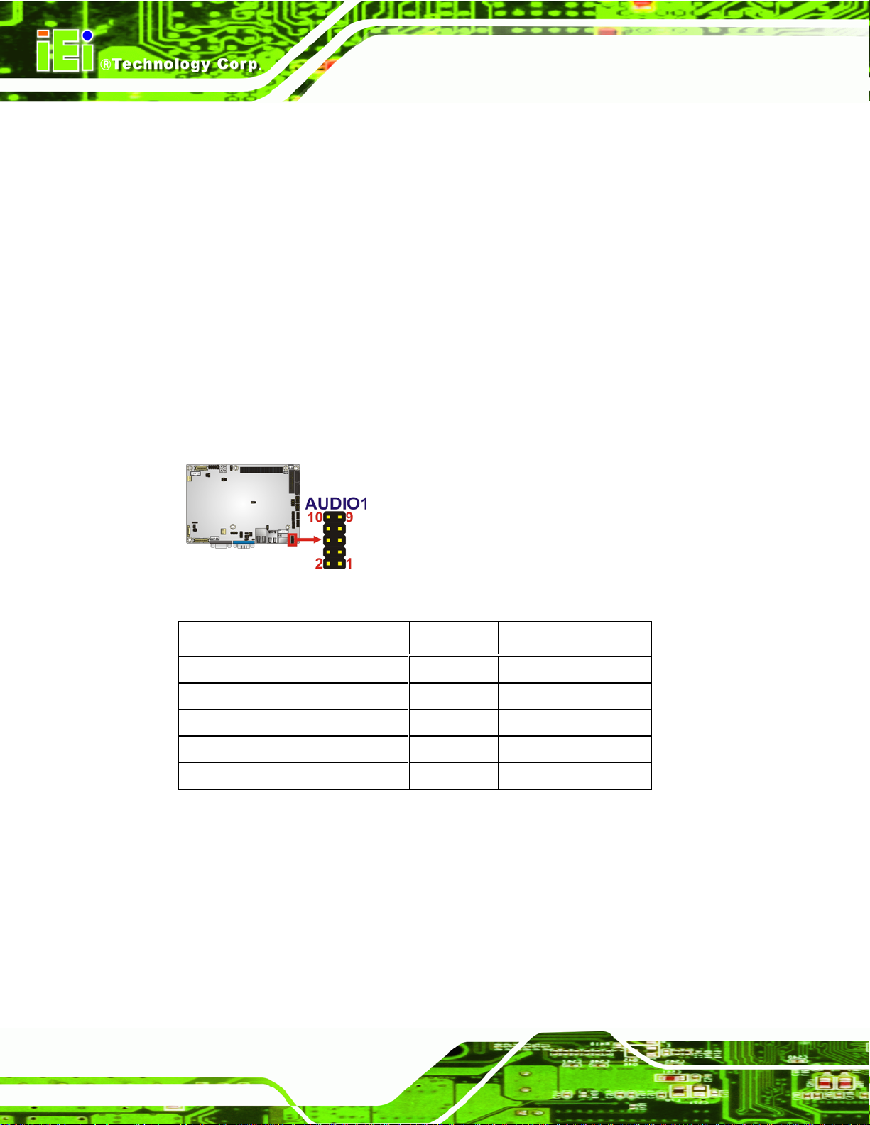
3.2.15 PCIe Mini Card Slot
CN Label: MINI-PCIE1
NANO-PV-D4252/N4552/D5252 EPIC SBC
CN Type:
CN Location:
CN Pinouts:
The PCIe Min
PCIe Mini card slot
6Figure 3-16
See
See Table 3-17
i card slot is for installing PCIe Mini expansion cards.
Figure 3-16: PCIe Mini Card Slot Location
Pin Description Pin Description
1 PCIE_WAKE# 2 VCC3
3 N/C 4 GND
5 N/C 6 1.5 V
Page 28
7 CLKREQ# 8 LFRAME#
9 GND 10 LAD3
11 CLK- 12 LAD2
13 CLK+ 14 LAD1
15 GND 16 LAD0
17 PCIRST# 18 GND
Page 43

NANO-PV-D4252/N4552/D5252 EPIC SBC
Pin Description Pin Description
19 LPC 20 VCC3
21 GND 22 PCIRST#
23 PERN2 24 3VDual
25 PERP2 26 GND
27 GND 28 1.5 V
29 GND 30 SMBCLK
31 PETN2 32 SMBDATA
33 PETP2 34 GND
35 GND 36 USBD37 GND 38 USBD+
39 VCC3 40 GND
41 VCC3 42 N/C
43 GND 44 RF_LINK#
45 SATATXP1 46 BLUELED#
47 SATATXN1 48 1.5 V
49 SATARXN1 50 GND
51 SATARXP1 52 VCC3
Table 3-17: PCIe Mini Card Slot Pinouts
3.2.16 Power Connector (+12 V, power supply)
CN Label: CPU12V1
CN Type:
CN Location:
CN Pinou
The co
ts:
nnector supports the 12 V power supply.
4-pin Molex power connector (1x4)
See Figure 3-17
See Table 3-18
Page 29
Page 44

NANO-PV-D4252/N4552/D5252 EPIC SBC
Figure 3-17: CPU 12V Power Connector Location
PIN NO. DESCRIPTION PIN NO. DESCRIPTION
1 GND 2 GND
3 +12V 4 +12V
Table 3-18: CPU 12V Power Connector Pinouts
3.2.17 SATA Drive Connectors
CN Label: SATA1, SATA2
CN Type:
CN Location:
CN Pinouts:
The two SATA 3Gb/s drive connectors are each connected to a SATA 3Gb/s drive. The
SATA 3Gb/s drives transfer data at speeds as high as 3.0 Gb/s.
7-pin SATA drive connectors
6Figure 3-18
See
6Table 3-19
See
Page 30
Figure 3-18: SATA Drive Connector Locations
PIN NO. DESCRIPTION
1 GND
2 TX+
3 TX-
Page 45
NANO-PV-D4252/N4552/D5252 EPIC SBC
4 GND
5 RX6 RX+
7 GND
Table 3-19: SATA Drive Connector Pinouts
3.2.18 SATA Power Connector
CN Label: PWR1
CN Type:
CN Location:
CN Pinouts:
2-pin wafer (1x2)
See Figure 3-19
See Table 3-20
The SATA Power Connector provides +5V power output to the SATA connectors.
Figure 3-19: SATA Power Connector Locations
PIN NO. DESCRIPTION
1 +5V
2 GND
Table 3-20: SATA Power Connector Pinouts
3.2.19 Serial Port Connectors (RS-232)
CN Label: COM2, COM4, COM5
CN Type:
CN Location:
CN Pinouts:
10-pin header (2x5)
6Figure 3-20
See
6Table 3-21
See
Page 31
Page 46
These connectors provide RS-232 communications.
NANO-PV-D4252/N4552/D5252 EPIC SBC
Figure 3-20: COM Connector Pinout Locations
PIN NO. DESCRIPTION PIN NO. DESCRIPTION
1 Data Carrier Direct (DCD) 2 Data Set Ready (DSR)
3 Receive Data (RXD) 4 Request To Send (RTS)
5 Transmit Data (TXD) 6 Clear To Send (CTS)
7 Data Terminal Ready (DTR) 8 Ring Indicator (RI)
9 Ground (GND) 10 GND
Page 32
Table 3-21: COM Connector Pinouts
Page 47
NANO-PV-D4252/N4552/D5252 EPIC SBC
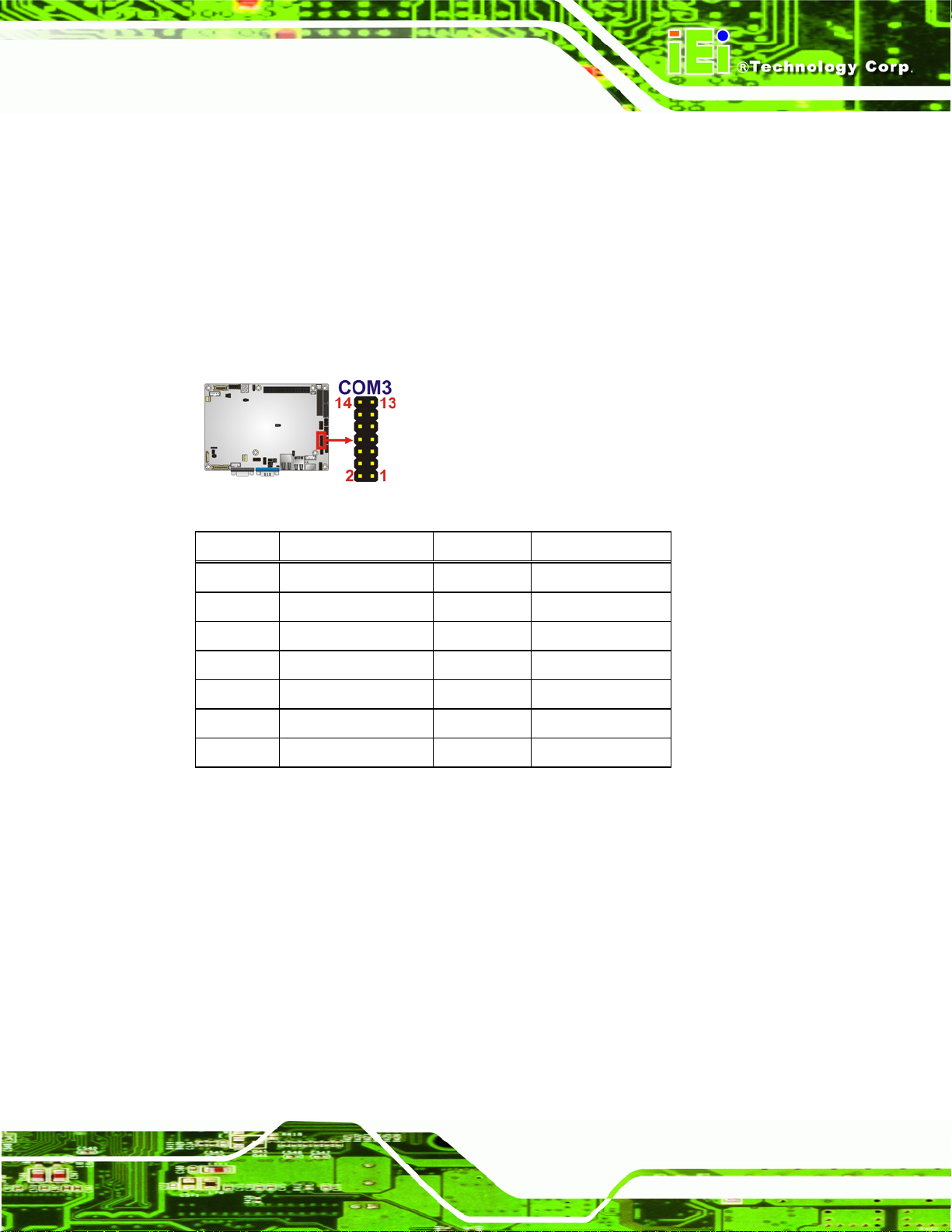
3.2.20 Serial Port Connector (RS-232/422/485)
CN Label: COM3
CN Type:
CN Location:
CN Pinouts:
14-pin header (2x7)
See Figure 3-21
See Table 3-22
Used for RS-232/422/485 communications.
Figure 3-21: Serial Port Connector Location
PIN NO. DESCRIPTION PIN NO. DESCRIPTION
1 DCD 2 DSR2
3 RXD 4 RTS2
5 TXD 6 CTS2
7 DTR 8 RI2
9 GND 10 N/A
11 RS422 TX2/485+ 12 RS422 TX2/48513 RS422 RX2+ 14 RS422 RX2-
Table 3-22: Serial Port Connector Pinouts
3.2.21 SMBus Connector
CN Label: CN1
CN Type:
CN Location:
CN Pinouts:
The SMBus Connector provides a connection to a SMBus (System Management Bus)
device.
4-pin wafer (1x4)
See Figure 3-19
See Table 3-20
Page 33
Page 48
NANO-PV-D4252/N4552/D5252 EPIC SBC
Figure 3-22: SMBus Connector Locations
PIN NO. DESCRIPTION
1 GND
2 SMBDATA
3 SMBCLK
4 VCC5S
Table 3-23: SMBus Connector Pinouts
3.2.22 SPI Flash Connector
CN Label: SPI1
CN Type:
CN Location:
CN Pinou
ts:
The 8-pin SPI Flash
8-pin header (2x4)
See Figure 3-23
See Table 3-24
connector is used to flash the BIOS.
Figure 3-23: SPI Flash Connector
Pin Description Pin Description
Page 34
1 VCC 2 GND
3 CS# 4 CLOCK
Page 49

NANO-PV-D4252/N4552/D5252 EPIC SBC
Pin Description Pin Description
5 SO 6 SI
7 NC 8 NC
Table 3-24: SPI Flash Connector Pinouts
3.2.23 USB Connectors
CN Label: USB0_1, USB2_3, USB4_5
CN Type:
CN Location:
CN Pinouts:
8-pin header (2x4)
See Figure 3-24
See Table 3-25
The USB connectors connect to USB devices. Each pin header provides two USB ports.
Figure 3-24: USB Connector Pinout Locations
PIN NO. DESCRIPTION PIN NO. DESCRIPTION
1 VCC 2 GND
3 DATA- 4 DATA+
5 DATA+ 6 DATA7 GND 8 VCC
Table 3-25: USB Port Connector Pinouts
Page 35
Page 50
NANO-PV-D4252/N4552/D5252 EPIC SBC
3.3 External Peripheral Interface Connector Panel
6Figure 3-25 shows the NANO-PV-D4252/N4552/D5252 external peripheral interface
connector (EPIC) panel. The NANO-PV-D4252/N4552/D5252 EPIC panel consists of the
following:
1 x Ethernet connector
1 x Keyboard/Mouse
1 x Serial port (RS-232)
2 x USB connectors
1 x VGA connector
Figure 3-25: NANO-PV-D4252/N4552/D5252 External Peripheral Interface
Connector
3.3.1 Ethernet Connector
CN Label: LAN1
CN Type:
CN Location:
CN Pinouts:
The NANO-PV-D4252/N4552/D5252 is equipped with one built-in RJ-45 Ethernet
controller. The controller can connect to the LAN through the RJ-45 LAN connector.
PIN DESCRIPTION PIN DESCRIPTION
1 LAN1_MDI0P 2 LAN1_MDI0N
3 LAN1_MDI1P 4 LAN1_MDI1N
RJ-45
6Figure 3-25
See
6Table 3-26
See
Page 36
5 +VCT_LAN1 6 GND
7 LAN1_MDI2P 8 LAN1_MDI2N
9 LAN1_MDI3P 10 LAN1_MDI3N
Page 51

NANO-PV-D4252/N4552/D5252 EPIC SBC
Table 3-26: LAN Pinouts
The RJ-45 Ethernet connector has two status LEDs, one green and one yello w. The green
LED indicates activity on the port and the yellow LED indicates the speed. See
3-27.
Speed LED Activity/Link LED
STATUS
Off 10 Mbps connection Off No link
Green 100 Mbps connection Yellow Linked
Orange Gbps connection Blinking TX/RX activity 1
Table 3-27: RJ-45 Ethernet Connector LEDs
DESCRIPTION STATUS DESCRIPTION
6Table
Figure 3-26: RJ-45 Ethernet Connector
3.3.2 Keyboard/Mouse Connector
CN Label: PT1
CN Type:
CN Location:
CN Pinou
The keyboard and mouse connector is a standard PS/2 connector.
ts:
PS/2
See Figure 3-25
See Figure 3-27 an
d Table 3-28
Figure 3-27: PS/2 Pinout and Configuration
Page 37
Page 52

Pin Description
1 KB DATA
2 MS DATA
3 GND
4 VCC
5 KB CLOCK
6 MS CLOCK
Table 3-28: Keyboard Connector Pinouts
3.3.3 USB Connectors
CN Label: USB6_7
NANO-PV-D4252/N4552/D5252 EPIC SBC
CN Type:
CN Location:
CN Pinouts:
The NANO-PV-D4252/N4552/D5252 has four external USB 2.0 ports. The ports connect
to both USB 2.0 and USB 1.1 devices.
PIN NO. DESCRIPTION PIN NO. DESCRIPTION
1 VCC 5 VCC
2 DATA- 6 DATA3 DATA+ 7 DATA+
4 GROUND 8 GROUND
Table 3-29: USB Port Connector Pinouts
3.3.4 VGA Connector
CN Label: VGA1
USB port
6Figure 3-25
See
6Table 3-29
See
Page 38
CN Type:
CN Location:
CN Pinouts:
15-pin Female
See Figure 3-25
See Figure 3-28 and Table 3-30
Page 53

NANO-PV-D4252/N4552/D5252 EPIC SBC
Connects to a monitor that accepts a standard VGA input.
Figure 3-28: VGA Connector
PIN DESCRIPTION PIN DESCRIPTION
1 RED 2 GREEN
3 BLUE 4 NC
5 GND 6 GND
7 GND 8 GND
9 VCC / NC 10 GND
11 NC 12 DDC DAT
13 HSYNC 14 VSYNC
15 DDCCLK
Table 3-30: VGA Connector Pinouts
Page 39
Page 54

NANO-PV-D4252/N4552/D5252 EPIC SBC
Chapter
4
4 Installation
Page 40
Page 55

NANO-PV-D4252/N4552/D5252 EPIC SBC
4.1 Anti-static Precautions
WARNING:
Failure to take ESD precautions during the installation of the
NANO-PV-D4252/N4552/D5252 may result in permanent damage to
the NANO-PV-D4252/N4552/D5252 and severe injury to the user.
Electrostatic discharge (ESD) can cause serious damage to electronic components,
including the NANO-PV-D4252/N4552/D5252. Dry climates are especially susceptible to
ESD. It is therefore critical that whenever the NANO-PV-D4252/N4552/D5252 or any
other electrical component is handled, the following anti-static precautions are strictly
adhered to.
Wear an anti-static wristband: Wearing a simple ant i-static wristband can
help to prevent ESD from damaging the board.
Self-grounding: Before handling the board, touch any grounded conducting
material. During the time the board is handled, frequently touch any
conducting materials that are connected to the ground.
Use an anti-static pad: When configuring the
NANO-PV-D4252/N4552/D5252, place it on an antic-static pad. This reduces
the possibility of ESD damaging the NANO-PV-D4252/ N4552/D5252.
Only handle the edges of the PCB: When handling the PCB, hold the PCB
by the edges.
Page 41
Page 56

NANO-PV-D4252/N4552/D5252 EPIC SBC
4.2 Installation Considerations
NOTE:
The following installation notices and installation considerations should
be read and understood before the NANO-PV-D4252/N4552/D5252 is
installed. All installation notices pertaining to the installation of the
NANO-PV-D4252/N4552/D5252 should be strictly adhered to. Failing
to adhere to these precautions may lead to severe damage of the
NANO-PV-D4252/N4552/D5252 and injury to the person installing the
motherboard.
4.2.1 Installation Notices
WARNING:
The installation instructions described in this manual should be carefully
followed in order to prevent damage to the
NANO-PV-D4252/N4552/D5252, NANO-PV-D4252/N4552/D5252
components and injury to the user.
Before and during the installation please DO the following:
Read the user manual:
o The user manual provides a complete description of the
NANO-PV-D4252/N4552/D5252 installation instructions and
configuration options.
Wear an electrostatic discharge cuff (ESD):
o Electronic components are easily damaged by ESD. Wearing an ESD cuff
removes ESD from the body and helps prevent ESD damage.
Place the NANO-PV-D4252/N4552/D5252 on an antistatic pad:
Page 42
o When installing or configuring the motherboard, place it on an antistatic
pad. This helps to prevent potential ESD damage.
Page 57

NANO-PV-D4252/N4552/D5252 EPIC SBC
Turn all power to the NANO-PV-D4252/N4552/D5252 off:
o When working with the NANO-PV-D4252/N4552/D5252, make sure that it
is disconnected from all power supplies and that no electri city is being fed
into the system.
Before and during the installation of the NANO-PV-D4252/N4552/D5252 DO NOT:
Remove any of the stickers on the PCB board. These stickers are required for
warranty validation.
Use the product before verifying all the cables and power connectors are
properly connected.
Allow screws to come in contact with the PCB circuit, connector pins, or its
components.
4.3 Unpacking
When the NANO-PV-D4252/N4552/D5252 is unpacked, please check all the unpacking
list items listed in Chapter 3 are indeed present. If any of the unpacking list items are not
available please contact the NANO-PV-D4252/N4552/D5252 vendor reseller/vendor
where the NANO-PV-D4252/N4552/D5252 was purchased or contact an IEI sales
representative.
4.4 SO-DIMM Installation
SO-DIMM is a critical component of the NANO-PV-D4252/N4552/D5252. If it is not
installed the NANO-PV-D4252/N4552/D5252 cannot run.
Page 43
Page 58

4.4.1 SO-DIMM Installation
To install an SO-DIMM, please follow the steps below and refer to Figure 4-1.
Figure 4-1: SO-DIMM Installation
Step 1: Locate the SO-DIMM socket. Place the board on an anti-static mat.
Step 2: Align the SO-DIMM with the socket. Align the notch on the memory with the
NANO-PV-D4252/N4552/D5252 EPIC SBC
notch on the memory socket.
Step 3: Insert the SO-DIMM. Push the memory in at a 20º angle. (See Figure 4-1)
Step 4: Seat th
Figure 4-1) Step 0:
e SO-DIMM. Gently push downwards and the arms clip into place. (See
4.5 Jumper Settings
NOTE:
A jumper is a metal bridge used to close an
electrical circuit. It consists of two or three metal
pins and a small metal clip (often protected by a
plastic cover) that slides over the pins to connect
them. To CLOSE/SHORT a jumper means
connecting the pins of the jumper with the plastic
clip and to OPEN a jumper means removing the
plastic clip from a jumper.
Page 44
Page 59

NANO-PV-D4252/N4552/D5252 EPIC SBC
Before the NANO-PV-D4252/N4552/D5252 is installed in the system, the jumpers must be
set in accordance with the desired configuration. The jumpers on the
NANO-PV-D4252/N4552/D5252 are listed in
6Table 4-1.
Description Type Label
AT Auto Button 2-pin header J_AUTOPWR1
Clear CMOS 3-pin header J_CMOS1
CompactFlash® Master/Slave function setting 2-pin header JCF1
CompactFlash® voltage select 2-pin header J_VCF1
COM3 RS-232/422/485 select 6-pin header J4
COM3 RS-422/485 select 6-pin header J6
COM3 RS-422 Termination select 2-pin header J10
COM3 RS-485 Termination select 2-pin header J9
LVDS1 LCD Voltage select 6-pin header J_VL VDS1
LVDS2 LCD Voltage select 6-pin header J_VL VDS2
LVDS1 LCD panel type 8-pin header J_LCD_TYPE1
LVDS2 LCD panel type 6-pin header JP2
Table 4-1: Jumpers
4.5.1 AT Auto Button Power Select Jumper Settings
Jumper Label: J_AUTOPWR1
Jumper Type:
Jumper Settings:
Jumper Loc
The AT Auto
ation:
Button Power Select jumper specifies the systems auto button power mode
as AT or ATX.
Setting Description
Short Use AT power
2-pin header
See Table 4-2
See Figure 4-2
Page 45
Page 60

Setting Description
Open Use ATX power
NANO-PV-D4252/N4552/D5252 EPIC SBC
Table 4-2: AT Auto Button Power Select Jumper Settings
Figure 4-2: AT Auto Button Select Jumper Settings
4.5.2 AT/ATX Power Select Jumper Settings
Jumper Label: J_ATXCTL1
Jumper Type:
Jumper Settings:
Jumper Loc
ation:
3-pin header (1x3)
See Table 4-3
See Figure 4-3
Page 46
The AT/ATX Power Sele
AT/ATX Power Select jumper settings are shown in Table 4-3.
AT Power Select Description
Short 1 - 2 Use ATX power
Short 2 – 3 Use AT power Default
Table 4-3: AT/ATX Power Select Jumper Settings
The location of the AT/ATX Power Select jumper is shown in Figure 4-3 below.
ct jumper specifies the systems power mode as AT or ATX.
Page 61
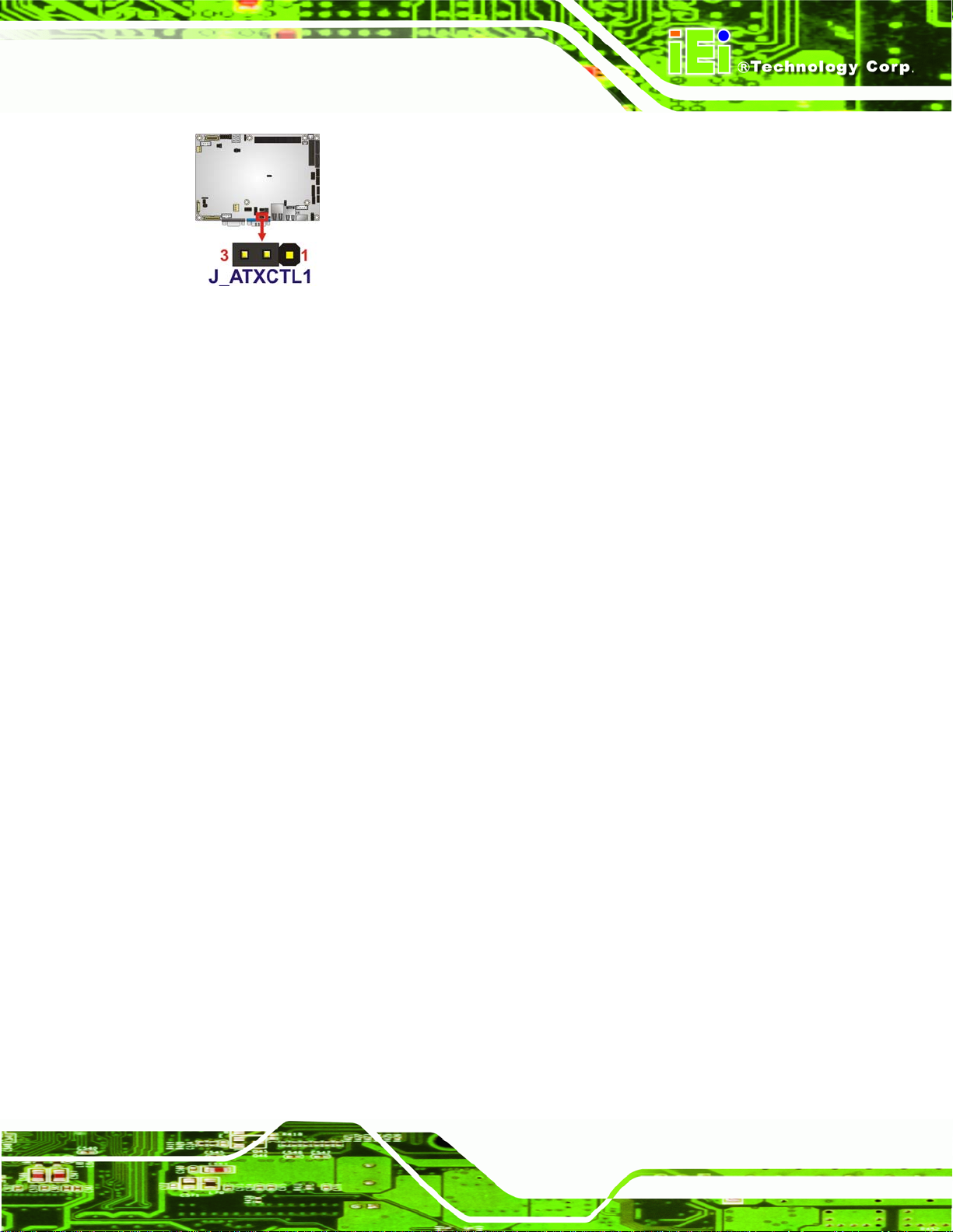
NANO-PV-D4252/N4552/D5252 EPIC SBC
Figure 4-3: AT/ATX Power Select Jumper Location
4.5.3 Clear CMOS Jumper
Jumper Label: J_CMOS1
Jumper Type:
Jumper Settings:
Jumper Location:
3-pin header (1x3)
6Table 4-4
See
6Figure 4-4
See
If the NANO-PV-D4252/N4552/D5252 fails to boot due to improper BIOS settings, the
clear CMOS jumper clears the CMOS data and resets the system BIOS information. To do
this, use the jumper cap to close pins 2 and 3 for a few seconds then reinstall the jumper
clip back to pins 1 and 2.
If the “CMOS Settings Wrong” message is displayed during the boot up process, the fault
may be corrected by pressing the F1 to enter the CMOS Setup menu. Do one of the
following:
Enter the correct CMOS setting
Load Optimal Defaults
Load Failsafe Defaults.
After having done one of the above, save the changes and exit the CMOS Setup menu.
The clear CMOS jumper settings are shown in
6Table 4-4.
Page 47
Page 62

Clear CMOS Description
Short 1 - 2 Keep CMOS Setup Default
Short 2 - 3 Clear CMOS Setup
Table 4-4: Clear CMOS Jumper Settings
The location of the clear CMOS jumper is shown in 6Figure 4-4 below.
Figure 4-4: Clear CMOS Jumper
4.5.4 COM 3 Function Select Jumper
NANO-PV-D4252/N4552/D5252 EPIC SBC
Jumper Label: J4
Jumper Type:
Jumper Settings:
Jumper Loc
The CO
ation:
M 3 Function Select jumper sets the communication protocol used by the second
6-pin header
See Table 4-5
See Figure 4-5
serial communications port (COM 3) as RS-232, RS-422 or RS -485. The COM 3 Function
Select settings are shown below.
Setting Description
1-2 RS-232
3-4 RS-422
5-6 RS-485
Table 4-5: COM 3 Function Select Jumper Settings
Page 48
Page 63

NANO-PV-D4252/N4552/D5252 EPIC SBC
Figure 4-5: COM 3 Function Select Jumper Location
4.5.5 COM 3 RS-422/485 Function Select Jumper
Jumper Label: J6
Jumper Type:
Jumper Settings:
Jumper Loc
The CO
serial communications port (COM 3) as RS-422 or RS-485. The COM 3 Function Select
settings are shown below.
Setting Description
1-3, 2-4 RS-422
3-5, 4-6 RS-485
Table 4-6: COM 3 RS-422/485 Function Select Jumper Settings
ation:
M 3 Function Select jumper sets the communication protocol used by the second
6-pin header
See Table 4-5
See Figure 4-5
Page 49
Page 64
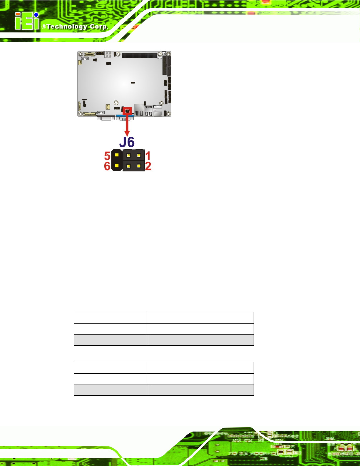
Figure 4-6: COM 3 RS-422/485 Function Select Jumper Location
NANO-PV-D4252/N4552/D5252 EPIC SBC
4.5.6 COM 3 RS-422/485 Termination Select Jumpers
Jumper Label: J9 and J10
Jumper Type:
Jumper Settings:
Jumper Loc
The CO
termination used by the serial COM 3 communications port as 120 ohm. The COM 3
RS-422 and RS-485 Termination Select settings are shown in Table 4-5 and Table 4-7.
ation:
M 3 RS-422 and RS-485 Termination Select jumpers enable or disable the
2-pin header
See Table 4-5 and Table 4-7
See Figure 4-7
RS-422 (J9) Setting Description
Short 120 ohm termination Resistance
Open NC (Default)
Table 4-7: COM 3 RS-422 Termination Select Jumper Settings
RS-485 (J10) Setting Description
Page 50
Short 120 ohm termination Resistance
Open NC (Default)
Table 4-8: COM 3 RS-485 Termination Select Jumper Settings
Page 65

NANO-PV-D4252/N4552/D5252 EPIC SBC
Figure 4-7: COM 3 RS-422 and RS-485 Termination Select Jumper
Location
4.5.7 CompactFlash® Card Setup
Jumper Label: JCF1
Jumper Type:
Jumper Settings:
Jumper Loc
CompactFlash® slot is connected through an IDE connection. This jumper sets the
The
CompactFlash® card as the master or slave IDE device.
Setting Description
Open Slave
Closed Master
Table 4-9: CompactFlash® Setup Jumper Settings
ation:
2-pin header
See Table 4-9
See Figure 4-4
Figure 4-8: CompactFlash® Setup Jumper Location
Page 51
Page 66
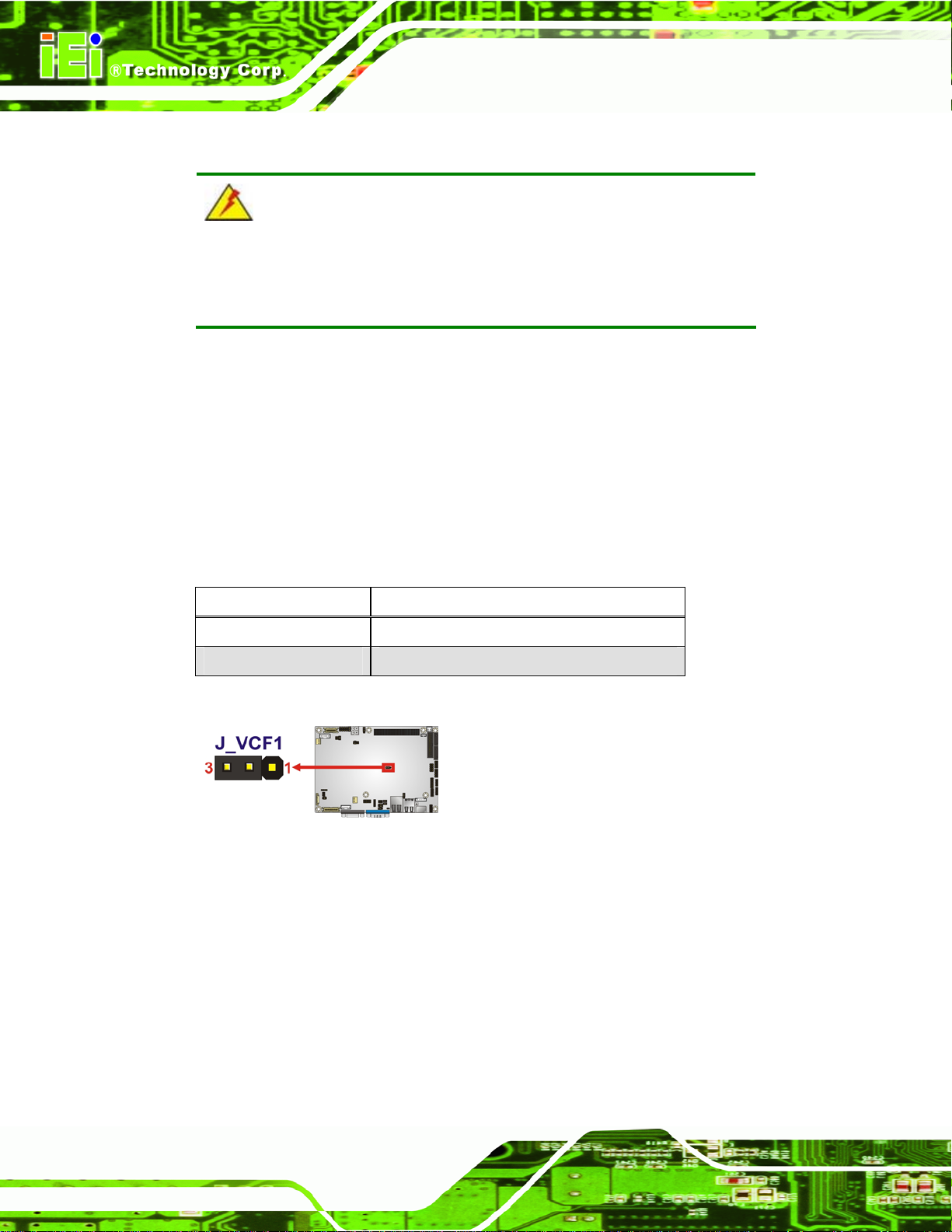
NANO-PV-D4252/N4552/D5252 EPIC SBC
4.5.8 CompactFlash® Voltage Selection
WARNING:
Incorrect voltages can destroy the CF card. Make sure to select a
voltage that matches the voltage required by the CF card.
Jumper Label: J_VCF1
Jumper Type:
Jumper Settings:
Jumper Loc
The Compa
the CF card.
Setting Description
Short 1-2 +5 V
Short 2-3 +3.3 V
Table 4-10: CompactFlash® Voltage Selection Jumper Settings
ation:
ctFlash® voltage selection jumper sets the voltage of the power supplied to
2-pin header
See Table 4-10
See Figure 4-9
Figure 4-9: CompactFlash® Voltage Selection Jumper Location
4.5.9 LVDS1 Screen Resolution Selection
Jumper Label: J_LCD_TYPE
8-pin header
See Table 4-11
See Figure 4-10
Page 52
Jumper Type:
Jumper Settings:
Jumper Loc
ation:
Page 67

NANO-PV-D4252/N4552/D5252 EPIC SBC
The LVDS1 Screen Resolution Selection jumper allows the LVDS screen voltage to be
set. The LVDS1 Screen Resolution Selection jumper settings are shown in Table 4-13.
Pin Description
Open 640 x 480
1-2 800 x 600
3-4 1024 x 768
1-2 and 3-4 1280 x 1024
5-6 1366 x 768
1-2 and 5-6 1920 x 1080
Table 4-11: LVDS1 Screen Resolution Jumper Settings
Figure 4-10: LVDS1 Screen Resolution Jumper Location
4.5.10 LVDS2 Screen Resolution Selection
Jumper Label: JP2
Jumper Type:
Jumper Settings:
Jumper Loc
ation:
6-pin header
See Table 4-13
See Figure 4-12
The LVDS
2 Screen Resolution Selection jumper allows the LVDS2 screen voltage to be
set. The LVDS2 Screen Resolution Selection jumper settings are shown in Table 4-13.
Pin Description
Open 640 x 480
1-2 800 x 600
3-4 1024 x 768
1-2 and 3-4 1280 x 1024
Page 53
Page 68

Pin Description
5-6 1366 x 768
1-2 and 5-6 1920 x 1080
NANO-PV-D4252/N4552/D5252 EPIC SBC
Table 4-12: LVDS2 Screen Resolution Jumper Settings
Figure 4-11: LVDS2 Screen Resolution Jumper Location
4.5.11 LVDS Voltage Selection
WARNING:
Incorrect voltages can destroy the LCD panel. Make sure to select a
voltage that matches the voltage required by the LCD panel.
Jumper Label: J_VLVDS1, J_VLVDS2
Page 54
Jumper Type:
Jumper Settings:
Jumper Loc
The LCD voltage sele
panel.
Setting Description
1-2 +3.3 V (Default)
3-4 +5.0 V
5-6 +12 V
Table 4-13: LVDS Voltage Selection Jumper Settings
ation:
6-pin header
See Table 4-13
See Figure 4-12
ction jumper sets the voltage of the power supplied to the LCD
Page 69

NANO-PV-D4252/N4552/D5252 EPIC SBC
Figure 4-12: LVDS Voltage Selection Jumper Locations
4.5.12 PCI-104 Voltage Setup
Jumper Label: JP1
Jumper Type:
Jumper Settings:
Jumper Loc
This jum
Setting Description
1-2 +5.0 V
2-3 +3.3 V
Table 4-14: PCI-104 Voltage Jumper Settings
ation:
per selects the voltage supplied to the PCI-104 expansion module.
3-pin header
See Table 4-14
See Figure 4-13
Figure 4-13: PCI-104 Voltage Jumper Location
Page 55
Page 70
4.6 Chassis Installation
4.6.1 Airflow
WARNING:
Airflow is critical to the cooling of the CPU and other onboard
components. The chassis in which the NANO-PV-D4252/N4552/ D5252
must have air vents to allow cool air to move into the system and hot air
to move out.
The NANO-PV-D4252/N4552/D5252 must be installed in a chassis with ventilation holes
on the sides allowing airflow to travel through the heat sink surface. In a system with an
individual power supply unit, the cooling fan of a power supply can also help generate
NANO-PV-D4252/N4552/D5252 EPIC SBC
airflow through the board surface.
4.6.2 Motherboard Installation
To install the NANO-PV-D4252/N4552/D5252 motherboard into the chassis please refer
to the reference material that came with the chassis.
4.7 Internal Peripheral Device Connections
This section outlines the installation of peripheral devices to the onboard connectors
4.7.1 AT/ATX Power Connection
Follow the instructions below to connect the NANO-PV-D4252/N4552/D5252 to an AT or
ATX power supply.
WARNING:
Page 56
Disconnect the power supply power cord from its AC power source to
prevent a sudden power surge to the NANO-PV-D4252/N4552/D5252.
Page 71

NANO-PV-D4252/N4552/D5252 EPIC SBC
Step 1: Locate the power cable. The power cable is shown in the packing list in
Chapter 3.
Step 2: Connect the Power Cable to the Motherboard. Connect the 4-pin (2x2) Molex
type power cable connector to the AT/ATX power connector on the motherboard.
See Figure 4-14.
Figure 4-14: Power Cable to Motherboard Connection
Step 3: Connect Power Cable to Power Supply. Connect one of the 4-pin (1x4) Molex
type power cable connectors to an AT/ATX power supply. See Figure 4-15.
Step 0:
Page 57
Page 72

NANO-PV-D4252/N4552/D5252 EPIC SBC
Figure 4-15: Connect Power Cable to Power Supply
4.7.2 Audio Kit Installation
The Audio Kit that came with the NANO-PV-D4252/N4552/D5252 connects to the audio
connector on the NANO-PV-D4252/N4552/D5252. The audio kit consists of three audio
jacks. Mic-in connects to a microphone. Line-in provides a stereo line-level input to
connect to the output of an audio device. Line-out, a stereo line-level output, connects to
two amplified speakers. To install the audio kit, please refer to the steps below:
Step 1: Locate the audio connector. The location of the 10-pin audio connector is
shown in Chapter 3.
Step 2: Align pin 1. Align pin 1 on the on-board connector with pin 1 on the audio kit
connector. Pin 1 on the audio kit connector is indicated with a white dot. See
Figure 4-16.
Page 58
Page 73
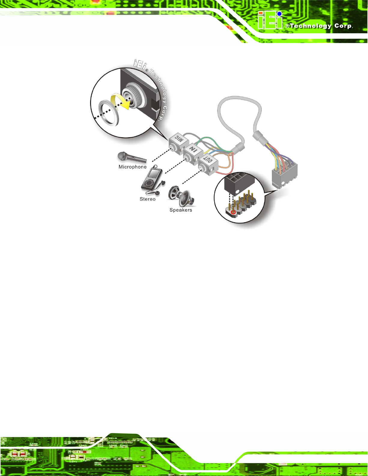
NANO-PV-D4252/N4552/D5252 EPIC SBC
Figure 4-16: Audio Kit Cable Connection
Step 3: Connect the audio devices. Connect speakers to the line-out audio jack.
Connect the output of an audio device to the line-in audio jack. Connect a
microphone to the mic-in audio jack.Step 0:
4.7.3 Single RS-232 Cable (w/o Bracket)
The single RS-232 cable consists of one serial port connector attached to a serial
communications cable that is then attached to a D-sub 9 male connector. To install the
single RS-232 cable, please follow the steps below.
Step 1: Locate the connector. The location of the RS-232 connector is shown in
Chapter 3.
Step 2: Insert the cable connector. Insert the connector into the serial port box header.
See Figure 4-17. A key on the front of the cabl
connector can only be installed in one direction.
e connectors ensures the
Page 59
Page 74

Figure 4-17: Single RS-232 Cable Installation
Step 3: Secure the bracket. The single RS-232 connector has two retention screws
NANO-PV-D4252/N4552/D5252 EPIC SBC
that must be secured to a chassis or bracket.
Step 4: Connect the serial device. Once the single RS-232 connector is connected to
a chassis or bracket, a serial communications device can be connected to the
system. Step 0:
4.8 External Peripheral Interface Connection
NOTE:
Due to limited space on the mainboard, the VGA and COM port on the
I/O panel cannot be used simultaneously. To utilize both the VGA and
COM port at the same time, please connect the RS-232 COM port
cable to the mainboard pin-header. For convenience, the mainboard
provides support for a maximum of four COM ports plus one VGA port
or five COM ports without VGA setup.
Page 60
Page 75

NANO-PV-D4252/N4552/D5252 EPIC SBC
The following external peripheral devices can be connected to the external peripheral
interface connectors.
Keyboard and mouse
RJ-45 Ethernet cable connector
Serial devices
USB devices
VGA monitor
To install these devices, connect the corresponding cable connector from the actual
device to the corresponding NANO-PV-D4252/N4552/D5252 external peripheral interface
connector making sure the pins are properly aligned.
4.8.1 LAN Connection (Single Connector)
There is one external RJ-45 LAN connector. The RJ-45 connector enables connection to
an external network. To connect a LAN cable with an RJ-45 connector, please follow the
instructions below.
Step 1: Locate the RJ-45 connectors. The location of the LAN connector is shown in
Chapter 4.
Step 2: Align the connectors. Align the RJ-45 connector on the LAN cable with one of
the RJ-45 connectors on the NANO-PV-D4252/N4552/D5252. See Figure 4-18.
Page 61
Page 76

Figure 4-18: LAN Connection
NANO-PV-D4252/N4552/D5252 EPIC SBC
Step 3: Insert the LAN cable RJ-45 connector. Once aligned, gently insert the LAN
cable RJ-45 connector into the on-board RJ-45 connector. Step 0:
4.8.2 PS/2 Y -Cable Connection
The NANO-PV-D4252/N4552/D5252 has a PS/2 connector on the external peripheral
interface panel. The dual PS/2 connector is connected to the PS/2 Y-cable that came with
the NANO-PV-D4252/N4552/D5252. One of the PS/2 cables is connected to a keyboard
and the other to a mouse to the system. Follow the steps below to connect a key board and
mouse to the NANO-PV-D4252/N4552/D5252.
Step 1: Locate the dual PS/2 connector. The location of the PS/2 connector is shown
in Chapter 3.
Step 2: Insert the keyboard/mouse connector. Insert the PS/2 connector on the end
of the PS/2 y-cable into the external PS/2 connector. See Figure 4-19.
Page 62
Page 77

NANO-PV-D4252/N4552/D5252 EPIC SBC
Figure 4-19: PS/2 Keyboard/Mouse Connector
Step 3: Connect the keyboard and mouse. Connect the keyboard and mouse to the
appropriate connector. The keyboard and mouse connectors can be
distinguished from each other by looking at the small graphic at the top of the
connector. Step 0:
4.8.3 Serial Device Connection
The NANO-PV-D4252/N4552/D5252 has a single female DB-9 connector on the external
peripheral interface panel for a serial device. Follow the steps below to connect a serial
device to the NANO-PV-D4252/N4552/D5252.
Step 1: Locate the DB-9 connector. The location of the DB-9 connector is shown in
Chapter 3.
Step 2: Insert the serial connector. Insert the DB-9 connector of a serial device into
the DB-9 connector on the external peripheral interface. See Figure 4-20.
Page 63
Page 78

NANO-PV-D4252/N4552/D5252 EPIC SBC
Figure 4-20: Serial Device Connector
Step 3: Secure the connector. Secure the serial device connector to the external
interface by tightening the two retention screws on either side of the connector.
4.8.4 USB Connection (Dual Connector)
The external USB Series "A" receptacle connectors provide easier and quicker access to
external USB devices. Follow the steps below to connect USB devices to the
NANO-PV-D4252/N4552/D5252.
Step 1: Locate the USB Series "A" receptacle connectors. The location of the USB
Series "A" receptacle connectors are shown in Chapter 3.
Step 2: Insert a USB Series "A" plug. Insert the USB Series "A" plug of a device into
the USB Series "A" receptacle on the external peripheral interface. See
Step 0:
Page 64
Figure 4-21. Step 0:
Page 79

NANO-PV-D4252/N4552/D5252 EPIC SBC
Figure 4-21: USB Connector
4.8.5 VGA Monitor Connection
The NANO-PV-D4252/N4552/D5252 has a single female DB-15 connector on the external
peripheral interface panel. The DB-15 connector is connected to a CRT or VGA monitor.
To connect a monitor to the NANO-PV-D4252/N4552/D5252, please follow the
instructions below.
Step 1: Locate the female DB-15 connector. The location of the female DB-15
connector is shown in Chapter 3.
Step 2: Align the VGA connector. Align the male DB-15 connector on the VGA screen
cable with the female DB-15 connector on the external peripheral interface.
Step 3: Insert the VGA connector. Once the connectors are properly aligned with the
insert the male connector from the VGA screen into the female connector on the
NANO-PV-D4252/N4552/D5252. See Figure 4-22.
Page 65
Page 80

Figure 4-22: VGA Connector
NANO-PV-D4252/N4552/D5252 EPIC SBC
Step 4: Secure the connector. Secure the DB-15 VGA connector from the VGA
monitor to the external interface by tightening the two retention screws on either
side of the connector. Step 0:
4.9 Software Installation
All the drivers for the NANO-PV-D4252/N4552/D5252 are on the CD that came with the
system. To install the drivers, please follow the steps below.
Step 1: Insert the CD into a CD drive connected to the system.
NOTE:
If the installation program doesn't start automatically:
Click "Start->My Computer->CD Drive->autorun.exe"
Step 2: The driver main menu appears (Figure 4-23).
Page 66
Page 81
NANO-PV-D4252/N4552/D5252 EPIC SBC
Figure 4-23: Introduction Screen
Step 3: Click NANO-PV-D4252/N4552/D5252.
Step 4: A new screen with a list of available drivers appears (Figure 4-24).
Page 67
Page 82

NANO-PV-D4252/N4552/D5252 EPIC SBC
Figure 4-24: Available Drivers
Step 5: Install all of the necessary drivers in this menu. Step 0:
Page 68
Page 83

NANO-PV-D4252/N4552/D5252 EPIC SBC
Chapter
5
5 BIOS Screens
Page 69
Page 84

5.1 Introduction
The BIOS is programmed onto the BIOS chip. The BIOS setup program allows changes to
certain system settings. This chapter outlines the options that can be changed.
5.1.1 Starting Setup
The AMI BIOS is activated when the computer is turned on. The setup program can be
activated in one of two ways.
NANO-PV-D4252/N4552/D5252 EPIC SBC
1. Press the D
2. Press the D
appears on the screen. 0.
If the message disappears before the D
again.
ELETE key as soon as the system is turned on or
ELETE key when the “Press Del to enter SETUP” message
ELETE key is pressed, restart the computer and try
5.1.2 Using Setup
Use the arrow keys to highlight items, press ENTER to select, use the PageUp and
PageDown keys to change entries, press F1 for help and press E
keys are shown in.
Key Function
Up arrow Move to previous item
Down arrow Move to next item
Left arrow Move to the item on the left hand side
SC to quit. Navigation
Page 70
Right arrow Move to the item on the right hand side
F1 key General help, only for Status Page Setup Menu and Option
Page Setup Menu
F2 key Load previous values.
F3 key Load optimized defaults
Page 85

NANO-PV-D4252/N4552/D5252 EPIC SBC
Key Function
F4 key Save all the CMOS changes
Esc key Main Menu – Quit and not save changes into CMOS
Status Page Setup Menu and Option Page Setup Menu --
Exit current page and return to Main Menu
Table 5-1: BIOS Navigation Keys
5.1.3 Getting Help
When F1 is pressed a small help window describing the appropriate keys to use and the
possible selections for the highlighted item appears. To exit the Help Window press E
the F1 key again.
5.1.4 Unable to Reboot After Configuration Changes
If the computer cannot boot after changes to the system configuration is made, CMOS
defaults. Use the jumper described in Chapter 4.
5.1.5 BIOS Menu Bar
The menu bar on top of the BIOS screen has the following main items:
Main – Changes the basic system configuration.
Advanced – Changes the advanced system settings.
Chipset – Changes the chipset settings.
Boot – Changes the system boot configuration.
Security – Sets User and Supervisor Passwords.
Save & Exit – Selects exit options and loads default settings
SC or
The following sections completely describe the configuration options found in the menu
items at the top of the BIOS screen and listed above.
Page 71
Page 86

S
NANO-PV-D4252/N4552/D5252 EPIC SBC
5.2 Main
The Main BIOS menu (BIOS Menu 1) appears when the BIOS Setup program is entered.
The Main menu gives an overview of the basic system information.
Aptio Setup Utility – Copyright (C) 2010 American Megatrends, Inc.
Main Advanced Chipset Boot Security Save & Exit
BIOS Information
BIOS Vendor American Megatrends
Core Version 4.6.4.0 0.20
Compliency UEFI 2.0
Project Version SA24AR11.ROM
Build Date 09/13/2010 20:29:21
System Date [Tue 09/23/2010]
System Time [14:20:27]
Access Level Administrator
Version 2.02.1205. Copyright (C) 2010 American Megatrends, Inc.
et the Time. Use Tab to
switch between Time
elements.
----------------------
: Select Screen
: Select Item
Enter Select
F1 General Help
F2 Previous Values
F3 Optimized Defaults
F4 Save
ESC Exit
BIOS Menu 1: Main
BIOS Information
The BIOS Information lists a brief summary of the BIOS. The fields in BIOS Information
cannot be changed. The items shown in the system overview include:
BIOS Vendor: Installed BIOS vendor
Core Version: Current BIOS version
Project Version: the board version
Build Date: Date the current BIOS version was made
The System Overview field also has two user configurable fields:
System Date [xx/xx/xx]
Use the System Date option to set the system date. Manually enter the day, month and
year.
Page 72
Page 87

NANO-PV-D4252/N4552/D5252 EPIC SBC
System Time [xx:xx:xx]
Use the System Time option to set the system time. Manually enter the hours, minutes
and seconds.
5.3 Advanced
Use the Advanced menu (BIOS Menu 2) to configure the CPU and peripheral devices
through the following sub-menus:
WARNING!
Setting the wrong values in the sections below may cause the system
to malfunction. Make sure that the settings made are compatible with
the hardware.
Aptio Setup Utility – Copyright (C) 2010 American Megatrends, Inc.
Main Advanced Chipset Boot Security Save & Exit
> ACPI Settings
> Trusted Computing
> CPU Configuration
> IDE Configuration
> USB Configuration
> Super IO Configuration
> H/M Monitor
> Serial Port Console Redirection
Version 2.02.1205. Copyright (C) 2010 American Megatrends, Inc.
BIOS Menu 2: Advanced
System ACPI Parameters
----------------------
: Select Item
Enter Select
F1 General Help
F2 Previous Values
F3 Optimized
Defaults
F4 Save
ESC Exit
5.3.1 ACPI Settings
: Select Screen
The ACPI Settings menu (BIOS Menu 3) configures the Advanced Configuration and
Power Interface (ACPI) options.
Page 73
Page 88

Aptio Setup Utility – Copyright (C) 2010 American Megatrends, Inc.
Advanced
ACPI Sleep State [S3 (Suspend to R…)]
Version 2.01.1204. Copyright (C) 2010 American Megatrends, Inc.
BIOS Menu 3: ACPI Settings
NANO-PV-D4252/N4552/D5252 EPIC SBC
Set the ACPI state used
for System suspend
----------------------
: Select Screen
: Select Item
Enter Select
F1 General Help
F2 Previous Values
F3 Optimized
Defaults
F4 Save
ESC Exit
ACPI Sleep State [S3 (Suspend to RAM)]
Use the ACPI Sleep State option to specify the sleep state the system enters when it is
not being used.
Suspend Disabled
S1 (CPU Stop
Clock)
S3 (Suspend to
RAM)
DEFAULT
The system enters S1(POS) sleep state. The
system appears off. The CPU is stopped; RAM is
refreshed; the system is running in a low power
mode.
The caches are flushed and the CPU is powered
off. Power to the RAM is maintained. The
computer returns slower to a working state, but
more power is saved.
5.3.2 Trusted Computing
Page 74
Use the Trusted Computing menu (BIOS Menu 4) to configure settings related to the
Trusted Computing Group (TCG) Trusted Platform Module (TPM).
Page 89

E
NANO-PV-D4252/N4552/D5252 EPIC SBC
Aptio Setup Utility – Copyright (C) 2010 American Megatrends, Inc.
Advanced
TPM Configuration
TPM SUPPORT [Disable]
Current TPM Status Information
NO TPM Hardware
Version 2.02.1205. Copyright (C) 2010 American Megatrends, Inc.
BIOS Menu 4: TPM Configuration
nables or Disables TPM
support. O.S. will not
show TPM. Reset of
platform is required.
----------------------
: Select Screen
: Select Item
Enter Select
F1 General Help
F2 Previous Values
F3 Optimized
Defaults
F4 Save
ESC Exit
TPM Support [Disable]
Use the TPM Support option to configure support for the TPM.
Disable DEFAULT
Enable
TPM support is disabled.
TPM support is enabled.
5.3.3 CPU Configuration
Use the CPU Configuration menu (BIOS Menu 5) to view detailed CPU specifications
and configure the CPU.
Page 75
Page 90

Aptio Setup Utility – Copyright (C) 2010 American Megatrends, Inc.
Advanced
CPU Configuration
Processor Type Intel(R) Atom(TM) CPU
CPU N475 @ 1.83GHz
EMT64 Supported
Processor Speed 1834 MHz
System Bus Speed 667 MHz
Ratio Status 11
Actual Ratio 11
Processor Stepping 106ca
Microcode Revision 263
L1 Cache RAM 56 k
L2 Cache RAM 512 k
Processor Core Single
Hyper-Threading Supported
Version 2.02.1205. Copyright (C) 2010 American Megatrends, Inc.
BIOS Menu 5: CPU Configuration
NANO-PV-D4252/N4552/D5252 EPIC SBC
----------------------
: Select Screen
: Select Item
Enter Select
F1 General Help
F2 Previous Values
F3 Optimized
Defaults
F4 Save
ESC Exit
The CPU Configuration menu (BIOS Menu 5) li
Processor Type: Lists the brand name of the CPU being u sed
EMT64: Indicates if the EM64T is supported by the CPU.
Processor Speed: Lists the CPU processing speed
System Bus: Lists the system bus
Ratio Status: List the maximum FSB divisor
Actual Ratio: Lists current FSB divisor
Processor Stepping: Lists the CPU processing stepping
Microcode Revision: Lists the microcode revision
L1 Cache RAM: Lists the CPU L1 cache size
L2 Cache RAM: Lists the CPU L2 cache size
Processor Core: Lists the number of the processor core
Hyper-Threading: Indicates if the Intel Hyper-Threading Technology is
supported by the CPU.
sts the following CPU details:
Page 76
Page 91
NANO-PV-D4252/N4552/D5252 EPIC SBC
5.3.4 SATA Configuration
Use the SATA Configuration menu (BIOS Menu 6) to change and/or set the
configuration of the SATA devices installed in the system.
Aptio Setup Utility – Copyright (C) 2010 American Megatrends, Inc.
Advanced
PATA Master Not Present
PATA Slave Not Present
SATA Port0 Not Present
SATA Port1 Not Present
SATA Port2 Not Present
SATA Port3 Not Present
ATA/IDE Configuration [Enhanced]
Configure SATA as [IDE]
Version 2.02.1205. Copyright (C) 2010 American Megatrends, Inc.
Select ATA/IDE
Configuration.
---------------------
: Select Screen
: Select Item
Enter Select
F1 General Help
F2 Previous Values
F3 Optimized
Defaults
F4 Save
ESC Exit
BIOS Menu 6: IDE Configuration
ATA/IDE Configurations [Enhanced]
Use the ATA/IDE Configurations option to configure the ATA/IDE controller.
Disabled
Compatible
Enhanced DEFAULT
Disables the on-board ATA/IDE controller.
Configures the on-board ATA/IDE controller to be in
compatible mode. In this mode, a SATA channel will
replace one of the IDE channels. This mode supports
up to 4 storage devices.
Configures the on-board ATA/IDE controller to be in
Enhanced mode. In this mode, IDE channels and SATA
channels are separated. This mode supports up to 6
storage devices. Some legacy OS do not support this
mode.
Page 77
Page 92

d
Configure SATA as [IDE]
Use the Configure SATA as option to configure SATA devices as normal IDE devices.
NANO-PV-D4252/N4552/D5252 EPIC SBC
IDE DEFAULT
AHCI
Configures SATA devices as normal IDE device.
Configures SATA devices as AHCI device.
5.3.5 USB Configuration
Use the USB Configuration menu (BIOS Menu 7) to read USB configuration information
and configure the USB settings.
Aptio Setup Utility – Copyright (C) 2010 American Megatrends, Inc.
Advanced
USB Configuration
USB Devices:
1 Keyboard
Legacy USB Support [Enabled]
Version 2.02.1205. Copyright (C) 2010 American Megatrends, Inc.
Enables Legacy USB
support. AUTO option
isables legacy support
if no USB devices are
connected. DISABLE
option will keep USB
devices available only
for EFI applications.
---------------------
: Select Screen
: Select Item
Enter Select
F1 General Help
F2 Previous Values
F3 Optimized
Defaults
F4 Save
ESC Exit
BIOS Menu 7: USB Configuration
USB Devices
The USB Devices Enabled field lists the USB devices that are enabled on the system
Page 78
Page 93

S
NANO-PV-D4252/N4552/D5252 EPIC SBC
Legacy USB Support [Enabled]
Use the Legacy USB Support BIOS option to enable USB mouse and USB keyboard
support. Normally if this option is not enabled, any attached USB mouse or USB keyboard
does not become available until a USB compatible operating system is fully booted with all
USB drivers loaded. When this option is enabled, any attached USB mouse or USB
keyboard can control the system even when there is no USB driver loaded onto the
system.
Enabled DEFAULT
Disabled
Auto
Legacy USB support enabled
Legacy USB support disabled
Legacy USB support disabled if no USB devices are
connected
5.3.6 Super IO Configuration
Use the Super IO Configuration menu (BIOS Menu 8) to set or change the
configurations for the FDD controllers, parallel ports and serial ports.
Aptio Setup Utility – Copyright (C) 2010 American Megatrends, Inc.
Advanced
Super IO Configuration
Super IO Chip Finteck F81865
> Serial Port 0 Configuration
> Serial Port 1 Configuration
> Serial Port 2 Configuration
> Serial Port 3 Configuration
> IrDA Configuration
> Parallel Port Configuration
Version 2.02.1205. Copyright (C) 2010 American Megatrends, Inc.
et Parameters of Serial
Port 0 (COMA)
---------------------
: Select Screen
: Select Item
Enter Select
F1 General Help
F2 Previous Values
F3 Optimized
Defaults
F4 Save
ESC Exit
BIOS Menu 8: Super IO Configuration
Page 79
Page 94

E
NANO-PV-D4252/N4552/D5252 EPIC SBC
5.3.6.1 Serial Port n Configuration
Use the Serial Port n Configuration menu (BIOS Menu 9) to configure the serial port n.
Aptio Setup Utility – Copyright (C) 2010 American Megatrends, Inc.
Advanced
Serial Port 0 Configuration
Serial Port [Enabled]
Device Settings IO=3F8h; IRQ=4
Change Settings [Auto]
Version 2.02.1205. Copyright (C) 2010 American Megatrends, Inc.
nable or Disable Serial
Port (COM)
---------------------
: Select Screen
: Select Item
Enter Select
F1 General Help
F2 Previous Values
F3 Optimized
Defaults
F4 Save
ESC Exit
BIOS Menu 9: Serial Port n Configuration Menu
5.3.6.1.1 Serial Port 0 Configuration
Serial Port [Enabled]
Use the Serial Port option to enable or disable the serial port.
Disabled
Enabled DEFAULT
Change Settings [Auto]
Use the Change Settings option to change the serial port IO port address and interrupt
address.
Auto DEFAULT
Disable the serial port
Enable the serial port
The serial port IO port address and interrupt address
are automatically detected.
IO=3F8h;
IRQ=4
Page 80
Serial Port I/O port address is 3F8h and the interrupt
address is IRQ4
Page 95

NANO-PV-D4252/N4552/D5252 EPIC SBC
IO=3F8h;
IRQ=3, 4
IO=2F8h;
IRQ=3, 4
5.3.6.1.2 Serial Port 1 Configuration
Serial Port [Enabled]
Use the Serial Port option to enable or disable the serial port.
Disabled
Enabled DEFAULT
Change Settings [Auto]
Use the Change Settings option to change the serial port IO port address and interrupt
Serial Port I/O port address is 3F8h and the interrupt
address is IRQ3 and IRQ4
Serial Port I/O port address is 2F8h and the interrupt
address is IRQ3 and IRQ4
Disable the serial port
Enable the serial port
address.
Auto DEFAULT
IO=2F8h;
IRQ=3
IO=3F8h;
IRQ=3, 4
IO=2F8h;
IRQ=3, 4
5.3.6.1.3 Serial Port 2 Configuration
Serial Port [Enabled]
Use the Serial Port option to enable or disable the serial port.
The serial port IO port address and interrupt address
are automatically detected.
Serial Port I/O port address is 2F8h and the interrupt
address is IRQ3
Serial Port I/O port address is 3F8h and the interrupt
address is IRQ3 and IRQ4
Serial Port I/O port address is 2F8h and the interrupt
address is IRQ3 and IRQ4
Disabled
Disable the serial port
Page 81
Page 96

NANO-PV-D4252/N4552/D5252 EPIC SBC
Enabled DEFAULT
Change Settings [Auto]
Use the Change Settings option to change the serial port IO port address and interrupt
address.
Auto DEFAULT
IO=3E8h;
IRQ=11
IO=3E8h;
IRQ=10, 11
IO=2E8h;
IRQ=10, 11
Enable the serial port
The serial port IO port address and interrupt address
are automatically detected.
Serial Port I/O port address is 3E8h and the interrupt
address is IRQ11
Serial Port I/O port address is 3E8h and the interrupt
address is IRQ10, 11
Serial Port I/O port address is 2E8h and the interrupt
address is IRQ10, 11
5.3.6.1.4 Serial Port 3 Configuration
Serial Port [Enabled]
Use the Serial Port option to enable or disable the serial port.
Disabled
Enabled DEFAULT
Change Settings [Auto]
Use the Change Settings option to change the serial port IO port address and interrupt
address.
Auto DEFAULT
Disable the serial port
Enable the serial port
The serial port IO port address and interrupt address
are automatically detected.
Page 82
Page 97

NANO-PV-D4252/N4552/D5252 EPIC SBC
IO=2E8h;
IRQ=10
IO=3E8h;
IRQ=10, 11
IO=2E8h;
IRQ=10, 11
Serial Port I/O port address is 2E8h and the interrupt
address is IRQ10
Serial Port I/O port address is 3E8h and the interrupt
address is IRQ10, 11
Serial Port I/O port address is 2E8h and the interrupt
address is IRQ10, 11
5.3.6.2 IrDA Configuration
Use the IrDA Configuration menu (BIOS Menu 9) to configure the serial port n.
Aptio Setup Utility – Copyright (C) 2010 American Megatrends, Inc.
Advanced
IrDA Configuration
IrDA [Enabled]
Device Settings Reset Required
Enable or Disable IrDA
---------------------
: Select Screen
: Select Item
Enter Select
F1 General Help
F2 Previous Values
F3 Optimized
Defaults
F4 Save
ESC Exit
Version 2.02.1205. Copyright (C) 2010 American Megatrends, Inc.
BIOS Menu 10: IrDA Configuration Menu
IrDA [Enabled]
Use the IrDA option to enable or disable the infrared function.
Disabled
Enabled DEFAULT
Disable the infrared function
Enable the infrared function
Page 83
Page 98

C
NANO-PV-D4252/N4552/D5252 EPIC SBC
5.3.6.3 Parallel Port Configuration
Use the Parallel Port Configuration menu (BIOS Menu 9) to configure the serial port n.
Aptio Setup Utility – Copyright (C) 2010 American Megatrends, Inc.
Advanced
Parallel Port Configuration
Parallel Port [Enabled]
Device Settings IO=378h; IRQ=7
Change Settings [Auto]
Device Mode [Printer Mode]
Version 2.02.1205. Copyright (C) 2010 American Megatrends, Inc.
hange the Printer Port
mode
---------------------
: Select Screen
: Select Item
Enter Select
F1 General Help
F2 Previous Values
F3 Optimized
Defaults
F4 Save
ESC Exit
BIOS Menu 11: Parallel Port Configuration Menu
Parallel Port [Enabled]
Use the Parallel Port option to enable or disable the parallel port.
Disabled
Enabled DEFAULT
Change Settings [Auto]
Use the Change Settings option to change the parallel port IO port address and interrupt
address.
Auto DEFAULT
IO=378h;
Disable the parallel port
Enable the parallel port
The parallel port IO port address and interrupt
address are automatically detected.
Parallel Port I/O port address is 378h and the
IRQ=7
IO=278h;
IRQ=7
Page 84
interrupt address is IRQ7
Parallel Port I/O port address is 278h and the
interrupt address is IRQ7
Page 99

NANO-PV-D4252/N4552/D5252 EPIC SBC
IO=3BCh;
IRQ=7
IO=378h
IO=278h
IO=3BCh
Device Mode [Printer Mode]
Use the Device Mode option to select the mode the parallel port operates in.
Configuration options are listed below.
Printer Mode Default
SPP Mode
EPP-1.9 and SPP Mode
EPP-1.7 and SPP Mode
ECP Mode
Parallel Port I/O port address is 3BCh and the
interrupt address is IRQ7
Parallel Port I/O port address is 378h
Parallel Port I/O port address is 278h
Parallel Port I/O port address is 3BCh
ECP and EPP 1.9 Mode
ECP and EPP 1.7 Mode
5.3.7 H/W Monitor
The H/W Monitor menu (BIOS Menu 12) shows the operating temperature, fan speeds
and system voltages.
Page 85
Page 100
Aptio Setup Utility – Copyright (C) 2010 American Megatrends, Inc.
Advanced
PC Health Status
CPU Temperature :+39 C
SYS Temperature :+40 C
CPU FAN Speed :4950 RPM
VCC3V :+3.344 V
V_core :+1.136 V
Vcc :+5.087 V
Vcc12 :+11.352 V
V1_5VDDR :+1.504 V
VSB3V :+3.360 V
VBAT :+3.316 V
CPU Smart Fan control [Auto Mode]
Temperature Bound1 60
Temperature Bound2 50
Temperature Bound3 40
Temperature Bound4 30
Version 2.02.1205. Copyright (C) 2010 American Megatrends, Inc.
NANO-PV-D4252/N4552/D5252 EPIC SBC
---------------------
: Select Screen
: Select Item
Enter Select
F1 General Help
F2 Previous Values
F3 Optimized
Defaults
F4 Save
ESC Exit
BIOS Menu 12: Hardware Health Configuration
PC Health Status
The following system parameters and values are shown. The system parameters that are
monitored are:
System Temperatures:
o CPU Temperature
o System Temperature
Fan Speeds:
o CPU Fan Speed
Voltages:
o V_core
o Vcc
o Vcc12
o V1_5VDDR
Page 86
o VSB3V
o VBAT
 Loading...