

Page 1
PCISA-PV-D4251/N4551/D5251 CPU Card
IEI Technology Corp.
MODEL:
PCISA-PV-D4251/N4551/D5251
Half-Size CPU Card for Intel® Atom CPU,
DDR3, VGA, LAN, SATA 3Gb/s,
USB, HD Audio, RoHS Compliant
User Manual
Rev. 1.04 – 1 July, 2013
Page i
Page 2
PCISA-PV-D4251/N4551/D5251 CPU Card
Revision
Date Version Changes
1 July, 2013 1.04 Modified Table 3-20: COM2 Pinouts
3 December, 2012 1.03 Modified Table 3-18: Parallel Port Connector Pinouts
Modified Section
25 July, 2011 1.02 Modified Table 3-17: LVDS LCD Connector Pinouts
7 December, 2010 1.01 Added model variations
Updated specifications
Added optional CPU fan installation instruction
10 September, 2010 1.00 Initial release
2.4: Optional Items
Page ii
Page 3

PCISA-PV-D4251/N4551/D5251 CPU Card
COPYRIGHT NOTICE
The information in this document is subject to change without prior notice in order to
improve reliability, design and function and does not represent a commitment on the part
of the manufacturer.
In no event will the manufacturer be liable for direct, indirect, special, incidental, or
consequential damages arising out of the use or inability to use the product or
documentation, even if advised of the possibility of such damages.
This document contains proprietary information protected by copyright. All rights are
Copyright
reserved. No part of this manual may be reproduced by any mechanical, electronic, or
other means in any form without prior written permission of the manufacturer.
TRADEMARKS
All registered trademarks and product names mentioned herein are used for identification
purposes only and may be trademarks and/or registered trademarks of their respective
owners.
Page iii
Page 4
PCISA-PV-D4251/N4551/D5251 CPU Card
Table of Contents
1 INTRODUCTION.......................................................................................................... 1
1.1 INTRODUCTION........................................................................................................... 2
1.2 MODEL VARIATIONS ................................................................................................... 2
1.3 BENEFITS ................................................................................................................... 3
1.4 FEATURES ................................................................................................................... 3
1.5 CONNECTORS ............................................................................................................. 4
1.6 DIMENSIONS............................................................................................................... 6
1.7 DATA FLOW................................................................................................................ 7
1.8 TECHNICAL SPECIFICATIONS ...................................................................................... 8
2 PACKING LIST........................................................................................................... 10
2.1 ANTI-STATIC PRECAUTIONS.......................................................................................11
2.2 UNPACKING PRECAUTIONS........................................................................................11
2.3 PACKING LIST ........................................................................................................... 12
2.4 OPTIONAL ITEMS...................................................................................................... 13
3 CONNECTORS ........................................................................................................... 14
3.1 PERIPHERAL INTERFACE CONNECTORS..................................................................... 15
3.1.1 Layout .............................................................................................................. 15
3.1.2 Peripheral Interface Connectors ..................................................................... 15
3.1.3 External Interface Panel Connectors............................................................... 17
3.2 INTERNAL PERIPHERAL CONNECTORS...................................................................... 17
3.2.1 ATX Power Supply Enable Connector............................................................. 17
3.2.2 Audio Connector .............................................................................................. 18
3.2.3 Battery Connector............................................................................................ 19
3.2.4 CompactFlash® Socket.................................................................................... 20
3.2.5 Digital Input/Output Connector....................................................................... 21
3.2.6 Fan Connector................................................................................................. 22
3.2.7 Floppy Disk Connector (34-pin)...................................................................... 23
3.2.8 Flash SPI ROM Connector.............................................................................. 24
3.2.9 Front Panel Connector.................................................................................... 25
Page iv
Page 5

PCISA-PV-D4251/N4551/D5251 CPU Card
3.2.10 IDE Connector............................................................................................... 26
3.2.11 Infrared Interface Connector ......................................................................... 27
3.2.12 Keyboard/Mouse Connector.......................................................................... 28
3.2.13 LCD Backlight Connector.............................................................................. 29
3.2.14 LVDS LCD connector.................................................................................... 30
3.2.15 Parallel Port Connector ................................................................................ 31
3.2.16 RS-232 Serial Port Connectors (COM1, COM3 and COM4 ) ...................... 32
3.2.17 RS-232/422/485 Serial Port Connector (COM2) .......................................... 33
3.2.18 SATA Drive Connectors ................................................................................. 33
3.2.19 SMBus Connector .......................................................................................... 34
3.2.20 USB Connectors (Internal)............................................................................ 35
3.3 EXTERNAL PERIPHERAL INTERFACE CONNECTOR PANEL ......................................... 36
3.3.1 CRT Connector ................................................................................................ 37
3.3.2 Ethernet Connectors ........................................................................................ 37
3.3.3 USB Connector ................................................................................................ 39
4 INSTALLATION .........................................................................................................40
4.1 ANTI-STATIC PRECAUTIONS...................................................................................... 41
4.2 INSTALLATION CONSIDERATIONS.............................................................................. 41
4.3 BASIC INSTALLATION ............................................................................................... 43
4.3.1 SO-DIMM Installation..................................................................................... 43
4.3.2 Airflow.............................................................................................................. 43
4.3.3 Backplane Installation..................................................................................... 44
4.3.4 CPU Card Installation..................................................................................... 44
4.3.5 Optional CPU Fan Installation ....................................................................... 44
4.4 JUMPER SETTINGS .................................................................................................... 45
4.4.1 CF Card Setup ................................................................................................. 46
4.4.2 Clear CMOS Jumper........................................................................................ 47
4.4.3 COM 2 Function Select Jumper....................................................................... 48
4.4.4 LVDS Voltage Selection.................................................................................... 49
4.4.5 LVDS Panel Resolution Selection.................................................................... 50
4.4.6 PCIe Interface Setup........................................................................................ 51
4.5 INTERNAL PERIPHERAL DEVICE CONNECTIONS........................................................ 52
4.5.1 SATA Drive Connection ................................................................................... 52
4.5.2 USB Cable (Dual Port) with Slot Bracket ....................................................... 54
Page v
Page 6

4.6 EXTERNAL PERIPHERAL INTERFACE CONNECTION ................................................... 55
4.6.1 LAN Connection............................................................................................... 55
4.6.2 USB Device Connection................................................................................... 56
4.6.3 VGA Monitor Connection ................................................................................ 57
4.7 SOFTWARE INSTALLATION........................................................................................ 58
5 BIOS.............................................................................................................................. 59
5.1 INTRODUCTION......................................................................................................... 60
5.1.1 Starting Setup................................................................................................... 60
5.1.2 Using Setup...................................................................................................... 60
5.1.3 Getting Help..................................................................................................... 61
5.1.4 Unable to Reboot After Configuration Changes.............................................. 61
5.1.5 BIOS Menu Bar................................................................................................ 61
5.2 MAIN........................................................................................................................ 62
5.3 ADVANCED ............................................................................................................... 63
PCISA-PV-D4251/N4551/D5251 CPU Card
5.3.1 T rusted Computing........................................................................................... 63
5.3.2 CPU Configuration.......................................................................................... 64
5.3.3 SATA Configuration......................................................................................... 66
5.3.4 USB Configuration........................................................................................... 67
5.3.5 Super IO Configuration ................................................................................... 68
5.3.5.1 Floppy Disk Controller Configuration...................................................... 69
5.3.5.2 Serial Port n Configuration....................................................................... 70
5.3.5.3 IrDA Configuration................................................................................... 73
5.3.5.4 Parallel Port Configuration....................................................................... 74
5.3.6 H/W Monitor.................................................................................................... 75
5.3.7 Serial Port Console Redirection...................................................................... 77
5.4 CHIPSET ................................................................................................................... 78
5.4.1 Host Bridge Configuration .............................................................................. 79
5.4.1.1 OnChip VGA Configuration..................................................................... 80
5.4.2 South Bridge Configuration............................................................................. 81
5.4.3 Intel IGD SWSCI OpRegion............................................................................. 82
5.5 BOOT........................................................................................................................ 84
5.6 SECURITY................................................................................................................. 86
5.7 EXIT......................................................................................................................... 87
A BIOS OPTIONS .......................................................................................................... 89
Page vi
Page 7
PCISA-PV-D4251/N4551/D5251 CPU Card
B TERMINOLOGY........................................................................................................ 92
C ONE KEY RECOVERY............................................................................................. 96
C.1 ONE KEY RECOVERY INTRODUCTION ...................................................................... 97
C.1.1 System Requirement ........................................................................................ 98
C.1.2 Supported Operating System........................................................................... 99
C.2 SETUP PROCEDURE FOR WINDOWS........................................................................ 100
C.2.1 Hardware and BIOS Setup ............................................................................ 100
C.2.2 Create Partitions........................................................................................... 101
C.2.3 Install Operating System, Drivers and Applications..................................... 104
C.2.4 Build-up Recovery Partition.......................................................................... 105
C.2.5 Create Factory Default Image ...................................................................... 107
C.3 SETUP PROCEDURE FOR LINUX...............................................................................112
C.4 RECOVERY TOOL FUNCTIONS .................................................................................115
C.4.1 Factory Restore..............................................................................................117
C.4.2 Backup System................................................................................................118
C.4.3 Restore Your Last Backup...............................................................................119
C.4.4 Manual .......................................................................................................... 120
C.5 OTHER INFORMATION ............................................................................................ 121
C.5.1 Using AHCI Mode or ALi M5283 / VIA VT6421A Controller ...................... 121
C.5.2 System Memory Requirement........................................................................ 123
D WA TCHDOG TIMER.............................................................................................. 124
E DIGITAL I/O INTERFACE..................................................................................... 127
E.1 INTRODUCTION ...................................................................................................... 128
E.2 DIO CONNECTOR PINOUTS.................................................................................... 128
E.3 ASSEMBLY LANGUAGE EXAMPLE .......................................................................... 128
F HAZARDOUS MATERIALS DISCLOSURE........................................................ 129
F.1 HAZARDOUS MATERIALS DISCLOSURE TABLE FOR IPB PRODUCTS CER TIFIED AS
ROHS COMPLIANT UNDER 2002/95/EC WITHOUT MERCURY ..................................... 130
Page vii
Page 8

PCISA-PV-D4251/N4551/D5251 CPU Card
List of Figures
Figure 1-1: PCISA-PV-D4251/N4551/D5251..................................................................................2
Figure 1-2: Connectors (Front Side).............................................................................................4
Figure 1-3: Connectors (Solder Side)...........................................................................................5
Figure 1-4: Dimensions (mm)........................................................................................................6
Figure 1-5: Data Flow Diagram......................................................................................................7
Figure 3-1: Connectors and Jumpers.........................................................................................15
Figure 3-2: ATX Power Supply Enable Connector Location....................................................17
Figure 3-3: Audio Connector Location.......................................................................................18
Figure 3-4: Battery Connector Location.....................................................................................19
Figure 3-5: CF Card Socket Location .........................................................................................20
Figure 3-6: DIO Connector Location...........................................................................................21
Figure 3-7: Fan Connector Locations.........................................................................................22
Figure 3-8: 34-pin FDD Connector Location..............................................................................23
Figure 3-9: Flash SPI ROM Connector Locations .....................................................................24
Figure 3-10: Front Panel Connector Location ...........................................................................25
Figure 3-11: IDE Device Connector Location ............................................................................26
Figure 3-12: Infrared Connector Pinout Locations ................................................................... 28
Figure 3-13: Keyboard/Mouse Connector Location..................................................................28
Figure 3-14: LCD Backlight Connector Location ......................................................................29
Figure 3-15: LVDS LCD Connector Location.............................................................................30
Figure 3-16: Parallel Port Connector Location..........................................................................31
Figure 3-17: RS-232 Connector Pinout Locations.....................................................................32
Figure 3-18: COM2 Location........................................................................................................33
Figure 3-19: SATA Drive Connector Locations.........................................................................34
Figure 3-20: SMBus Connector Location...................................................................................35
Figure 3-21: Internal USB Connector Locations ....................................................................... 36
Figure 3-22: External Peripheral Interface Connector..............................................................36
Figure 3-23: VGA Connector .......................................................................................................37
Figure 3-24: RJ-45 Ethernet Connector......................................................................................38
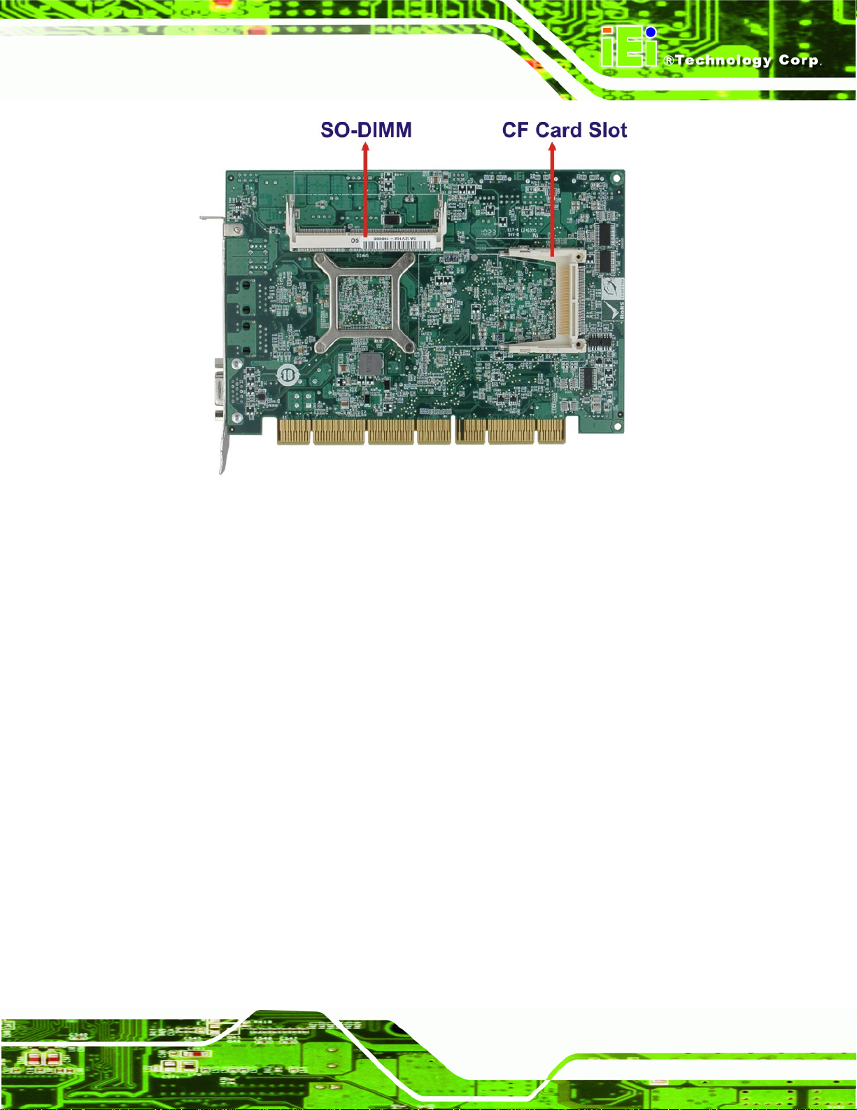
Figure 4-1: SO-DIMM Installation................................................................................................43
Page viii
Page 9

PCISA-PV-D4251/N4551/D5251 CPU Card
Figure 4-2: Connect Fan Cable....................................................................................................45
Figure 4-3: CF Card Setup Jumper Location.............................................................................47
Figure 4-4: Clear CMOS Jumper .................................................................................................48
Figure 4-5: COM 2 Function Select Jumper Location...............................................................49
Figure 4-6: LVDS Voltage Selection Jumper Pinout Locations...............................................50
Figure 4-7: LVDS Resolution Selection Jumper Pinout Locations .........................................51
Figure 4-8: PCIe Slot Jumper Location ......................................................................................52
Figure 4-9: SATA Drive Cable Connection.................................................................................53
Figure 4-10: SATA Power Drive Connection..............................................................................54
Figure 4-11: Dual USB Cable Connection..................................................................................55
Figure 4-12: LAN Connection......................................................................................................56
Figure 4-13: USB Device Connection.........................................................................................57
Figure 4-14: VGA Connector .......................................................................................................58
Figure C-1: IEI One Key Recovery Tool Menu...........................................................................97
Figure C-2: Launching the Recovery Tool.............................................................................. 101
Figure C-3: Recovery Tool Setup Menu .................................................................................. 102
Figure C-4: Command Mode..................................................................................................... 102
Figure C-5: Partition Creation Commands.............................................................................. 103
Figure C-6: Launching the Recovery Tool.............................................................................. 105
Figure C-7: System Configuration for Windows .................................................................... 105
Figure C-8: Build-up Recovery Partition................................................................................. 106
Figure C-9: Press any key to continue.................................................................................... 106
Figure C-10: Press F3 to Boot into Recovery Mode............................................................... 107
Figure C-11: Recovery Tool Menu ........................................................................................... 107
Figure C-12: About Symantec Ghost Window........................................................................ 108
Figure C-13: Symantec Ghost Path ......................................................................................... 108
Figure C-14: Select a Local Source Drive ............................................................................... 109
Figure C-15: Select a Source Partition from Basic Drive ...................................................... 109
Figure C-16: File Name to Copy Image to ............................................................................... 110
Figure C-17: Compress Image.................................................................................................. 110
Figure C-18: Image Creation Confirmation............................................................................. 111
Figure C-19: Image Creation Complete................................................................................... 111
Figure C-20: Image Creation Complete................................................................................... 111
Figure C-21: Press Any Key to Continue................................................................................ 112
Figure C-22: Partitions for Linux.............................................................................................. 113
Page ix
Page 10

Figure C-23: System Configuration for Linux......................................................................... 114
Figure C-24: Access menu.lst in Linux (Text Mode).............................................................. 114
Figure C-25: Recovery Tool Menu ........................................................................................... 115
Figure C-26: Recovery Tool Main Menu.................................................................................. 116
Figure C-27: Restore Factory Default...................................................................................... 117
Figure C-28: Recovery Complete Window.............................................................................. 117
Figure C-29: Backup System.................................................................................................... 118
Figure C-30: System Backup Complete Window ................................................................... 118
Figure C-31: Restore Backup................................................................................................... 119
Figure C-32: Restore System Backup Complete Window..................................................... 119
Figure C-33: Symantec Ghost Window ................................................................................... 120
PCISA-PV-D4251/N4551/D5251 CPU Card
Page x
Page 11
PCISA-PV-D4251/N4551/D5251 CPU Card
List of Tables
Table 1-1: Model Variations...........................................................................................................3
Table 1-2: Technical Specifications..............................................................................................9
Table 2-1: Packing List.................................................................................................................13
Table 2-2: Optional Items.............................................................................................................13
Table 3–1: Internal Peripheral Connectors ................................................................................16
Table 3–2: External Peripheral Connectors...............................................................................17
Table 3-3: ATX Power Supply Enable Connector Pinouts .......................................................18
Table 3-4: AT/ATX Power Mode Setting .....................................................................................18
Table 3-5: Audio Connector Pinouts ..........................................................................................19
Table 3-6: Battery Connector Pinouts........................................................................................19
Table 3-7: CF Card Socket Pinouts.............................................................................................21
Table 3-8: DIO Connector Pinouts..............................................................................................22
Table 3-9: Fan Connector Pinouts..............................................................................................23
Table 3-10: 34-pin FDD Connector Pinouts ...............................................................................24
Table 3-11: Flash SPI ROM Connector Pinouts.........................................................................25
Table 3-12: Front Panel Connector Pinouts...............................................................................26
Table 3-13: IDE Connector Pinouts.............................................................................................27
Table 3-14: Infrared Connector Pinouts.....................................................................................28
Table 3-15: Keyboard/Mouse Connector Pinouts .....................................................................29
Table 3-16: LCD Backlight Connector Pinouts..........................................................................30
Table 3-17: LVDS LCD Connector Pinouts ................................................................................30
Table 3-18: Parallel Port Connector Pinouts .............................................................................31
Table 3-19: RS-232 Connector Pinouts ......................................................................................32
Table 3-20: COM2 Pinouts...........................................................................................................33
Table 3-21: SATA Drive Connector Pinouts...............................................................................34
Table 3-22: SMBus Connector Pinouts ......................................................................................35
Table 3-23: USB3 and USB4 Pinouts..........................................................................................36
Table 3-24: VGA Connector Pinouts...........................................................................................37
Table 3-25: LAN1 and LAN2 Pinouts ..........................................................................................38
Table 3-26: RJ-45 Ethernet Connector LEDs.............................................................................38
Page xi
Page 12

Table 3-27: External USB Connector Pinouts............................................................................39
Table 4-1: Jumpers.......................................................................................................................46
Table 4-2: CF Card Setup Jumper Settings ...............................................................................46
Table 4-3: Clear CMOS Jumper Settings....................................................................................47
Table 4-4: COM 2 Function Select Jumper Settings.................................................................48
Table 4-5: LVDS Voltage Selection Jumper Settings................................................................50
Table 4-6: LVDS Resolution Selection Jumper Settings..........................................................51
Table 4-7: PCIe Slot Jumper Setting...........................................................................................51
Table 5-1: BIOS Navigation Keys................................................................................................61
PCISA-PV-D4251/N4551/D5251 CPU Card
Page xii
Page 13

PCISA-PV-D4251/N4551/D5251 CPU Card
BIOS Menus
BIOS Menu 1: Main.......................................................................................................................62
BIOS Menu 2: Advanced..............................................................................................................63
BIOS Menu 3: TPM Configuration...............................................................................................64
BIOS Menu 4: CPU Configuration...............................................................................................65
BIOS Menu 5: IDE Configuration.................................................................................................66
BIOS Menu 6: USB Configuration...............................................................................................67
BIOS Menu 7: Super IO Configuration........................................................................................68
BIOS Menu 8: Floppy Disk Controller Configuration Menu .....................................................69
BIOS Menu 9: Serial Port n Configuration Menu.......................................................................70
BIOS Menu 10: IrDA Configuration Menu...................................................................................73
BIOS Menu 11: Parallel Port Configuration Menu.....................................................................74
BIOS Menu 12: Hardware Health Configuration........................................................................76
BIOS Menu 13: Serial Port Console Redirection.......................................................................77
BIOS Menu 14: Chipset................................................................................................................78
BIOS Menu 15: Host Bridge Chipset Configuration..................................................................79
BIOS Menu 16: OnChip VGA Configuration...............................................................................80
BIOS Menu 17:South Bridge Chipset Configuration.................................................................81
BIOS Menu 18:South Bridge Chipset Configuration.................................................................82
BIOS Menu 19: Boot.....................................................................................................................84
BIOS Menu 20: Security...............................................................................................................86
BIOS Menu 21:Exit........................................................................................................................87
Page xiii
Page 14
PCISA-PV-D4251/N4551/D5251 CPU Card
1 Introduction
Chapter
1
Page 1
Page 15
1.1 Introduction
PCISA-PV-D4251/N4551/D5251 CPU Card
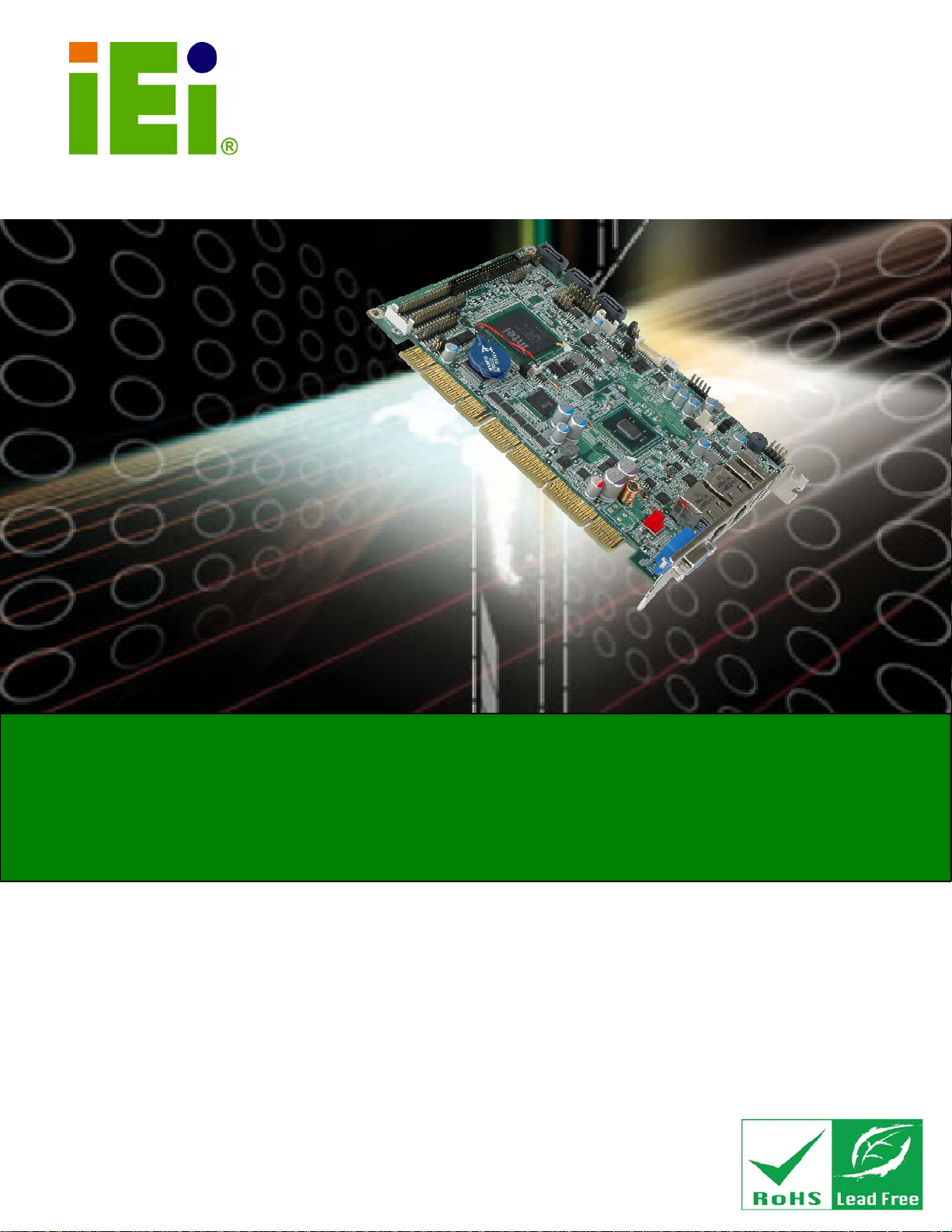
Figure 1-1: PCISA-PV-D4251/N4551/D5251
The PCISA-PV-D4251/N4551/D5251 half-size PCISA CPU card is an Intel® Atom
dual-core CPU platform. The PCISA-PV-D4251/N4551/D5251 comes with a DDR3
SO-DIMM socket, VGA interface and dual PCI Express (PCIe) Gigabit Ethernet (GbE).
The PCISA-PV-D4251/N4551/D5251 supports up to three, second-generation serial ATA
(SATA) hard disk drives (HDD) with maximum transfer rates of 3Gb/s and up to six USB
2.0 devices. The PCISA-PV-D4251/N4551/D5251 also has a Co m pactFlash ® card socket
for additional system storage. Multiple display support adds versatility to the system
enabling system integrators and designers increased flexibility in selecting display panel
options.
1.2 Model Variations
The PCISA-PV series has six models. The model variations are list below.
TM
Page 2
Model Name CPU CPU Core TPM
PCISA-PV-D5251 Intel® Atom D525 Dual core No
PCISA-PV-D5251T Intel® Atom D525 Dual core Yes
Page 16

PCISA-PV-D4251/N4551/D5251 CPU Card
PCISA-PV-D4251 Intel® Atom D425 Single core No
PCISA-PV-D4251T Intel® Atom D425 Single core Yes
PCISA-PV-N4551 Intel® Atom N455 Single core No
PCISA-PV-N4551T Intel® Atom N455 Single core Yes
Table 1-1: Model Variations
1.3 Benefits
Some of the PCISA-PV-D4251/N4551/D5251 motherboard benefits include:
Powerful graphics
Staying connected with both wired LAN connections
Speedy running of multiple programs and applications
1.4 Features
Some of the PCISA-PV-D4251/N4551/D5251 motherboard features are listed below:
RoHS compliant
Supports Intel® Atom™ dual-core/single-core processor
Supports one 204-pin 2 GB (max.) 800 MHz DDR3 SDRAM SO-DIMM
Dual PCIe GbE connectors
Supports three SATA drives with transfer rates up to 3Gb/s
Supports six USB 2.0 devices
Supports four serial ports
Support 18-bit LVDS and VGA for dual display
Page 3
Page 17
1.5 Connectors
The connectors on the PCISA-PV-D4251/N4551/D5251 are shown in the figure belo w.
PCISA-PV-D4251/N4551/D5251 CPU Card
Page 4
Figure 1-2: Connectors (Front Side)
Page 18
PCISA-PV-D4251/N4551/D5251 CPU Card
Figure 1-3: Connectors (Solder Side)
Page 5
Page 19
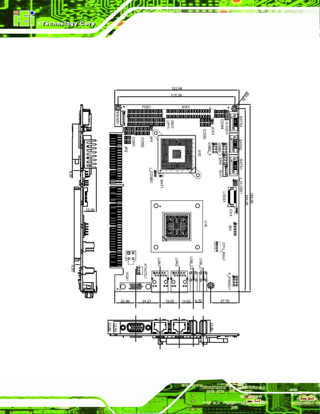
1.6 Dimensions
The main dimensions of the PCISA-PV-D4251/N4551/D5251 are shown in the diagram
below.
PCISA-PV-D4251/N4551/D5251 CPU Card
Page 6
Figure 1-4: Dimensions (mm)
Page 20
PCISA-PV-D4251/N4551/D5251 CPU Card
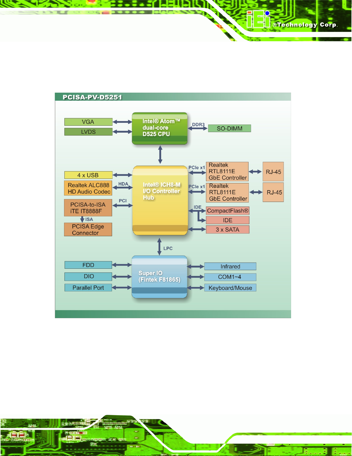
1.7 Data Flow
5Figure 1-5 shows the data flow between the system chipset, the CPU and other
components installed on the motherboard.
Figure 1-5: Data Flow Diagram
Page 7
Page 21
PCISA-PV-D4251/N4551/D5251 CPU Card
1.8 Technical Specifications
PCISA-PV-D4251/N4551/D5251 technical specifications are shown below.
Specifications PCISA-PV-D4251/N4551/D5251
CPU Supported
Chipset
Memory
Graphic Engine
Integrated Graphics
BIOS
Digital I/O
Intel® Atom D525 dual core processor (1.80GHz/1MB L2 cache)
Intel® Atom D425 single core processor (1.80GHz/512KB L2 cache)
Intel® Atom N455 single core processor (1.66GHz/512KB L2 cache)
Intel® ICH8M
One 204-pin 800 MHz DDR3 SDRAM SO-DIMM (system max. 2 GB)
Intel® GMA3150
D525/D425: Gen 3.5 DX9, 400 MHz
N455: Gen 3.5 DX9, 200 MHz
Analog CRT (CRT hot plug supported)
D525/D425: up to 2048 x 1536
N455: up to 1400 x 1050
18-bit single-channel LVDS supports up to WXGA 1366x768 or XGA
1024x768 resolution
UEFI BIOS
8-bit, 4-bit input/4-bit output
Ethernet Controllers
Super I/O Controller
Watchdog Timer
Audio
Expansion
TPM (Optional)
I/O Interface
CompactFlash®
Page 8
Two Realtek RTL8111E PCIe GbE controllers
(LAN1 supports ASF2.0)
Fintek F81865
Software programmable supports 1~2 55 sec. system reset
Realtek ALC888 HD Audio codec
4 x PCI bus
ISA bus supported by ITE IT8888G PCI-to-ISA bridge
On-board Infineon trusted platform module (TPM) SLB9635 TT1.2
One CompactFlahs® Type II slot
Page 22
PCISA-PV-D4251/N4551/D5251 CPU Card
Fan connector
Keyboard/Mouse
Serial Ports
USB 2.0/1.1 ports
Infrared
Parallel Port
Serial ATA
Floppy Disk Drive
IDE
Environmental and Power Specifications
Power Supply
Power Consumption
One 4-pin wafer for CPU fan
One internal 6-pin wafer connector
Three RS-232 COM connectors
One RS-232/422/485 COM connector
Four internal via pin header
Two external USB ports
One infrared connector
One parallel port via 26-pin header
Three independent SATA channels with 3.0 Gb/s data transfer rates
One FDD connector via 34-pin header
One IDE connector via 44-pin box header
AT/ATX supported; 5 V or 12 V by PCISA bus
12 V @ 0.57 A
5 V @ 3.36 A
(1.8 GHz Intel® Atom D525 dual-core CPU with one 1 GB 1066 MHz
DDR3 SO-DIMM)
12 V @ 0.42 A
5 V @ 1.52 A
(1.66GHz Intel Atom™ N455 single-core CPU with one 1 GB
1066 MHz DDR3 running 3Dmark®2001)
Operating temperature
Humidity
Physical Specifications
Dimensions
Weight (Gross/Net)
Table 1-2: Technical Specifications
D525: -20ºC ~ 60ºC with free air; -20ºC ~ 70ºC with force air
D425: -20ºC ~ 65ºC with free air; -20ºC ~ 70ºC with force air
N455: -20ºC ~ 70ºC with free air; -20ºC ~ 75ºC with force air
5% ~ 95% (non-condensing)
185 mm x 127.6 mm
1000 g / 250 g
Page 9
Page 23
PCISA-PV-D4251/N4551/D5251 CPU Card
Chapter
2
2 Packing List
Page 10
Page 24
PCISA-PV-D4251/N4551/D5251 CPU Card
2.1 Anti-static Precautions
WARNING!
Static electricity can destroy certain electronics. Make sure to follow the
ESD precautions to prevent damage to the product, and injury to the
user.
Make sure to adhere to the following guidelines:
Wear an anti-static wristband: Wearing an anti-static wristband can prevent
electrostatic discharge.
Self-grounding: Touch a grounded conductor every few minutes to discharge
any excess static buildup.
Use an anti-static pad: When configuring any circuit board, place it on an
anti-static mat.
Only handle the edges of the PCB: Don't touch the surface of the
motherboard. Hold the motherboard by the edges when handling.
2.2 Unpacking Precautions
When the PCISA-PV-D4251/N4551/D5251 is unpacked, please do the following:
Follow the antistatic guidelines above.
Make sure the packing box is facing upwards whe n opening.
Make sure all the packing list items are present.
Page 11
Page 25
2.3 Packing List
NOTE:
If any of the components listed in the checklist below are missing, do
not proceed with the installation. Contact the IEI reseller or vendor the
PCISA-PV-D4251/N4551/D5251 was purchased from or contact an IEI
PCISA-PV-D4251/N4551/D5251 CPU Card
sales representative directly by sending an email to
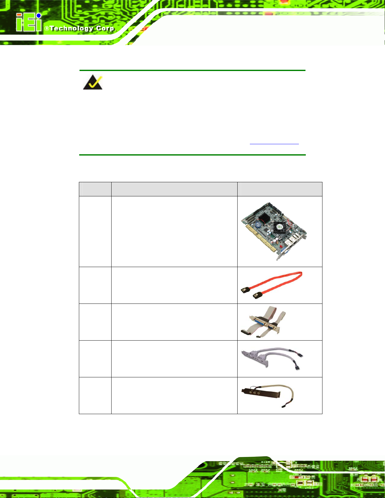
The PCISA-PV-D4251/N4551/D5251 is shipped with the following components:
Quantity Item and Part Number Image
1 PCISA-PV-D4251,
PCISA-PV-N4551,
PCISA-PV-D5251,
PCISA-PV-D4251T,
PCISA-PV-N4551T or
PCISA-PV-D5251T
3 SATA cable
(P/N: 32000-062800-RS)
1 LPT/RS-232 cable
(P/N:19800-000027-RS)
32sales@iei.com.tw.
Page 12
1 USB cable
(P/N: CB-USB02-RS
1 Audio cable
(P/N: 19800-000111-RS)
Page 26
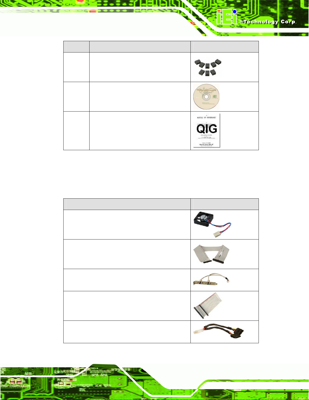
PCISA-PV-D4251/N4551/D5251 CPU Card
Quantity Item and Part Number Image
1 Mini jumper pack (2.0mm)
(P/N:33100-000033-RS)
1 Utility CD
1 Quick Installation Guide
Table 2-1: Packing List
2.4 Optional Items
The following are optional components which may be separately purchased:
Item and Part Number Image
CPU fan
(P/N: 19FTS00032100-000001-RS)
FDD cable
(P/N: 32200-000058-RS)
KB/MS cable
(P/N: 19800-000075-RS)
ATA 66/10 0 flat cable
(P/N: 32200-000037-RS)
SATA power cable
(P/N: 32102-000100-200-RS)
Table 2-2: Optional Items
Page 13
Page 27

PCISA-PV-D4251/N4551/D5251 CPU Card
Chapter
3
3 Connectors
Page 14
Page 28
PCISA-PV-D4251/N4551/D5251 CPU Card
3.1 Peripheral Interface Connectors
This chapter details all the jumpers and connectors.
3.1.1 Layout
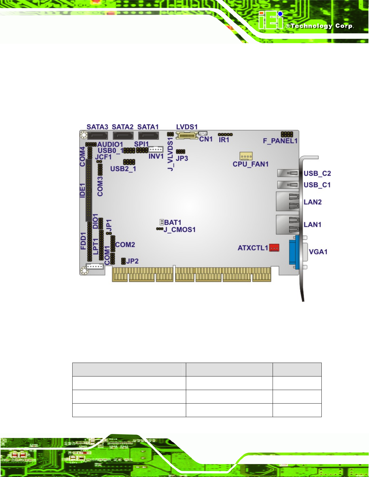
The figure below shows all the connectors and jumpers.
Figure 3-1: Connectors and Jumpers
3.1.2 Peripheral Interface Connectors
The table below lists all the connectors on the board.
Connector Type Label
ATX enable connector 3-pin wafer ATXCTL1
Audio connector 10-pin header AUDIO1
Battery connector 2-pin wafer BAT1
Page 15
Page 29

Connector Type Label
CompactFlash® card slot 50-pin slot (solder side) CF1
DDR3 DIMM socket 204-pin slot (solder side) DIMM1
Digital input/output connector 10-pin header DIO1
Fan connector, CPU 4-pin wafer connector CPU_FAN1
FDD connector 34-pin header FDD1
Flash SPI ROM connector 8-pin header SPI1
Front panel connector 8-pin header F_PANEL1
IDE Interface connector 44-pin box header IDE1
Infrared interface connector 5-pin header IR1
Keyboard/Mouse connector 6-pin wafer KB/MS1
LCD backlight connector 5-pin wafer connector INV1
PCISA-PV-D4251/N4551/D5251 CPU Card
LVDS LCD connector 20-pin crimp connector LVDS1
Parallel port connector 26-pin header LPT1
RS-232 serial port connector 10-pin header COM1
RS-232/422/485 serial port connector 14-pin header COM2
RS-232 serial port connector 10-pin header COM3
RS-232 serial port connector 10-pin header COM4
SATA drive conne ctor (1) 7-pin SATA connector SATA1
SATA drive conne ctor (2) 7-pin SATA connector SATA2
SATA drive conne ctor (3) 7-pin SATA connector SATA3
SMBus connector 4-pin wafer connector CN1
USB connector (1) 8-pin header USB0_1
USB connector (2) 8-pin header USB2_1
Table 3–1: Internal Peripheral Connectors
Page 16
Page 30
PCISA-PV-D4251/N4551/D5251 CPU Card
3.1.3 External Interface Panel Connectors
The table below lists the connectors on the external I/O panel.
Connector Type Label
CRT connector 15-pin female
connector
Ethernet connector (1) RJ-45 connector LAN1
Ethernet connector (2) RJ-45 connector LAN2
USB 2.0 port (1) USB port connector USB_C1
USB 2.0 port (2) USB port connector USB_C2
Table 3–2: External Peripheral Connectors
3.2 Internal Peripheral Connectors
The section describes all of the connectors on the PCISA-PV-D4251/N4551/D52 51.
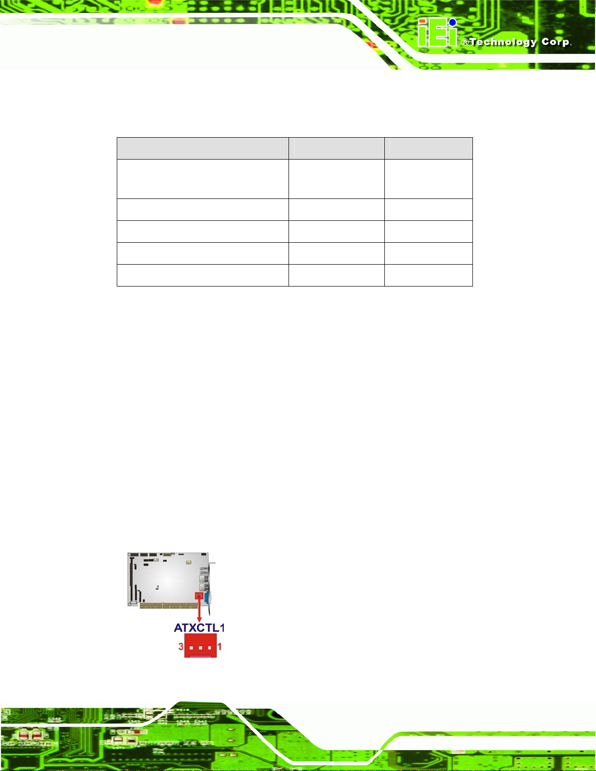
3.2.1 ATX Power Supply Enable Connector
CN Label: ATXCTL1
CN Type:
3-pin wafer (1x3)
VGA1
Figure 3-2
CN Location:
CN Pinouts:
The ATX power supply enable connector enables the PCISA-PV-D4251/N4551/D5251 to
be connected to an ATX power supply.
See
See
Table 3-3
Figure 3-2: ATX Power Supply Enable Connector Location
Page 17
Page 31

PIN NO. DESCRIP TIO N
1 +5V Standby
2 PS-ON
3 GND
Table 3-3: ATX Power Supply Enable Connector Pinouts
The AT/ATX power mode settings are listed below.
PIN NO. DESCRIP TIO N
AT Mode Short 2-3
ATX Mode Use PS_ON# and 5VSB cable
Table 3-4: AT/ATX Power Mode Setting
3.2.2 Audio Connector
PCISA-PV-D4251/N4551/D5251 CPU Card
CN Label: AUDIO1
CN Type:
CN Location:
CN Pinouts:
10-pin header (2x5)
Figure 3-3
See
Table 3-5
See
The audio connector connects to the optional audio cable.
Figure 3-3: Audio Connector Location
Page 18
Page 32

PCISA-PV-D4251/N4551/D5251 CPU Card
PIN NO. DESCRIPTION PIN NO. DESCRIPTION
1 SPK_R 2 LINE1R
3 GND 4 GND
5 SPK_L 6 LINE1L
7 GND 8 GND
9 FMIC1R 10 FMIC1L
Table 3-5: Audio Connector Pinouts
3.2.3 Battery Connector
CN Label: BAT1
CN Type:
CN Location:
CN Pinouts:
2-pin wafer (1x2)
Figure 3-4
See
Table 3-6
See
This is connected to the system battery. The battery provides power to the system clock to
retain the time when power is turned off.
Figure 3-4: Battery Connector Location
Pin Description
1 Battery+ (+3V)
2 Ground
Table 3-6: Battery Connector Pinouts
Page 19
Page 33

3.2.4 CompactFlash® Socket
PCISA-PV-D4251/N4551/D5251 CPU Card
CN Label:
CN Type:
CN Location:
CN Pinouts:
CF1 (solder side)
50-pin slot (2x25)
Figure 3-5
See
Table 3-7
See
A CF Type I or Type II memory card is inserted to the CF socket on the solder side of the
PCISA-PV-D4251/N4551/D5251.
Figure 3-5: CF Card Socket Location
PIN NO. DESCRIPTION PIN NO. DESCRIPTION
1 GROUND 26 VCC-IN CHECK1
2 DATA 3 27 DATA 11
3 DATA 4 28 DATA 12
4 DATA 5 29 DATA 13
5 DATA 6 30 DATA 14
6 DATA 7 31 DATA 15
7 HDC_CS0# 32 HDC_CS1
8 N/C 33 N/C
9 GROUND 34 IOR#
10 N/C 35 IOW#
11 N/C 36 VCC_COM
12 N/C 37 IRQ15
13 VCC_COM 38 VCC_COM
14 N/C 39 CSEL
15 N/C 40 N/C
Page 20
Page 34
PCISA-PV-D4251/N4551/D5251 CPU Card
16 N/C 41 HDD_RESET
17 N/C 42 IORDY
18 SA2 43 SDREQ
19 SA1 44 SDACK#
20 SA0 45 HDD_ACTIVE#
21 DATA 0 46 66DET
22 DATA 1 47 DATA 8
23 DATA 2 48 DATA 9
24 N/C 49 DATA 10
25 VCC-IN CHECK2 50 GROUND
Table 3-7: CF Card Socket Pinouts
3.2.5 Digital Input/Output Connector
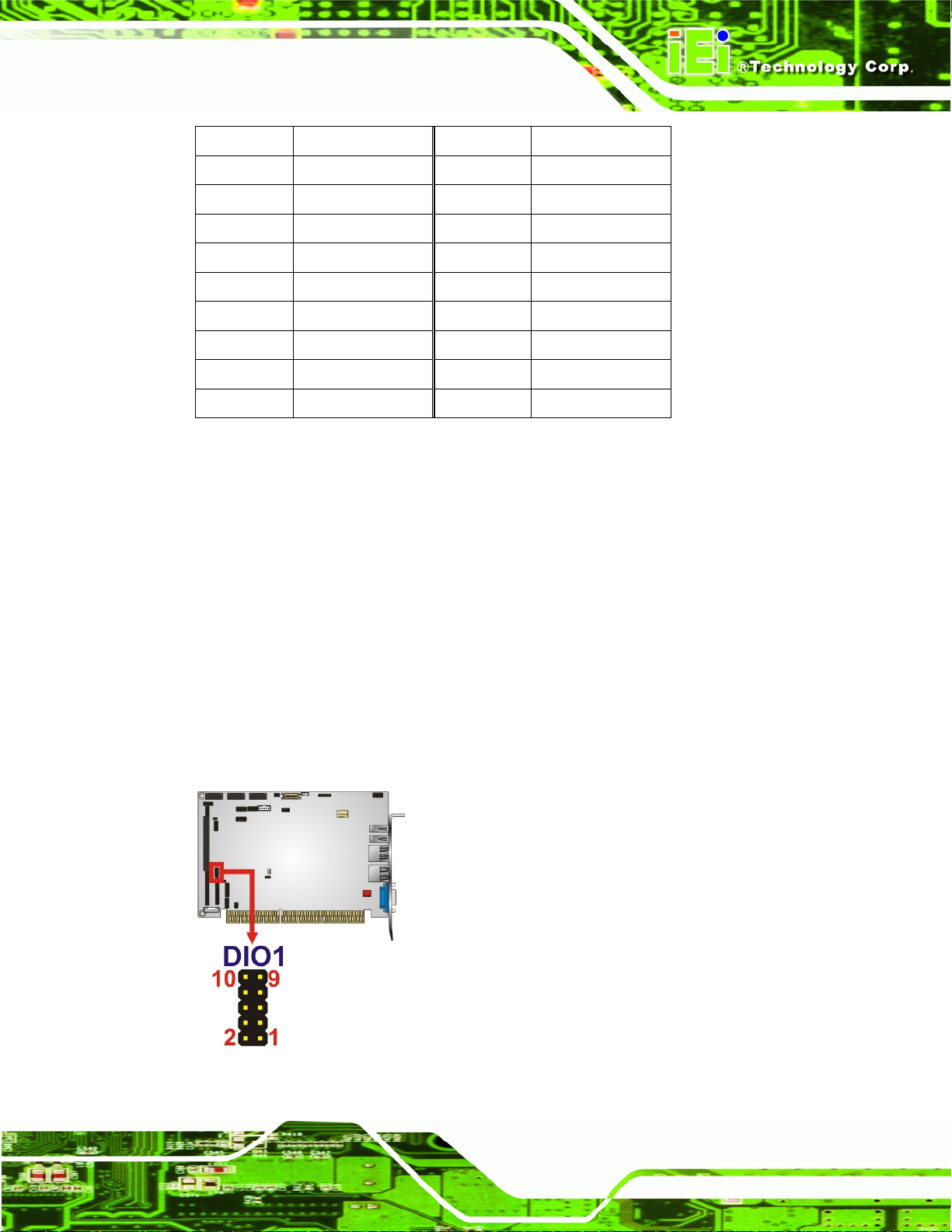
CN Label: DIO1
CN Type:
CN Location:
CN Pinouts:
10-pin header (2x5)
Figure 3-6
See
Table 3-8
See
The DIO connector is managed through a Super I/O chip. The DIO connector pins are
user programmable. The digital IO port of PCISA-PV-D4251/N4551/D5251 is 5V CMOS
level.
Figure 3-6: DIO Connector Location
Page 21
Page 35
PIN NO. DESCRIPTION PIN NO. DESCRIPTION
1 GND 2 +5 V
3 OUTPUT 3 4 OUTPUT 2
5 OUTPUT 1 6 OUTPUT 0
7 INPUT 3 8 INPUT 2
9 INPUT 1 10 INPUT 0
Table 3-8: DIO Connector Pinouts
3.2.6 Fan Connector
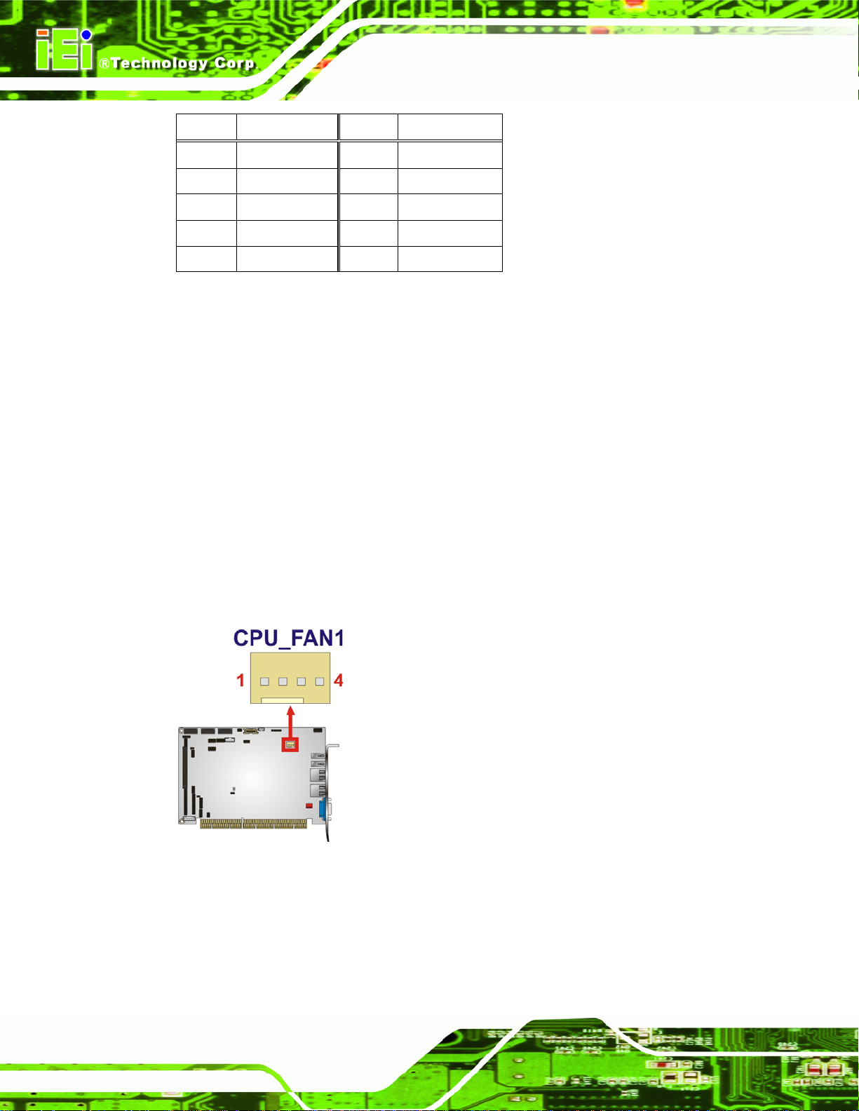
CN Label: CPU_FAN1
PCISA-PV-D4251/N4551/D5251 CPU Card
CN Type:
CN Location:
CN Pinouts:
The cooling fan connector provides a 12V, 500mA current to a CPU cooling fan. The
connector has a "rotation" pin to get rotation signals from fans and notify the system so the
system BIOS can recognize the fan speed. Please note that only specified fans can issue
the rotation signals.
4-pin wafer connector (1x4)
Figure 3-7
See
Table 3-9
See
Page 22
Figure 3-7: Fan Connector Locations
Page 36

PCISA-PV-D4251/N4551/D5251 CPU Card
IN NO.
1 GND
2 +12V
3 Sense
4 Control
ESCRIPTION
Table 3-9: Fan Connector Pinouts
3.2.7 Floppy Disk Connector (34-pin)
CN Label: FDD1
CN Type:
CN Location:
CN Pinouts:
The floppy disk connector is connected to a floppy disk drive.
34-pin header (2x17)
Figure 3-8
See
Table 3-10
See
Figure 3-8: 34-pin FDD Connector Location
PIN NO. DESCRIPTION PIN NO. DESCRIPTION
1 GND 2 REDUCE WRITE
3 GND 4 N/C
5 N/C 6 N/C
7 GND 8 INDEX#
9 GND 10 MOTOR ENABLE A#
11 GND 12 DRIVE SELECT B#
13 GND 14 DRIVE SELECT A#
Page 23
Page 37

15 GND 16 MOTOR ENABLE B#
17 GND 18 DIRECTION#
19 GND 20 STEP#
21 GND 22 WRITE DATA#
23 GND 24 WRITE GATE#
25 GND 26 TRACK 0#
27 GND 28 WRITE PROTECT#
29 GND 30 READ DATA#
31 GND 32 SIDE 1 SELECT#
33 GND 34 DISK CHANGE#
Table 3-10: 34-pin FDD Connector Pinouts
3.2.8 Flash SPI ROM Connector
PCISA-PV-D4251/N4551/D5251 CPU Card
CN Label: SPI1
CN Type:
CN Location:
CN Pinouts:
8-pin header (2x4)
Figure 3-9
See
Table 3-11
See
Use the Flash SPI ROM connector to flash SPI ROM.
Page 24
Figure 3-9: Flash SPI ROM Connector Locations
Page 38

PCISA-PV-D4251/N4551/D5251 CPU Card
PIN NO. DESCRIPTION PIN NO. DESCRIPTION
1 3.3V 2 GND
3 SPI_CS 4 SPI_CLK
5 SPI_SO 6 SPI_SI
7 NC 8 NC
Table 3-11: Flash SPI ROM Connector Pinouts
3.2.9 Front Panel Connector
CN Label: F_PANEL1
CN Type:
CN Location:
CN Pinouts:
The front panel connector connects to several external switches and indicators to monitor
and control the motherboard. These indicators and switches include:
Power LED
Power button
Reset button
HDD LED
8-pin header (2x4)
Figure 3-10
See
Table 3-12
See
Figure 3-10: Front Panel Connector Location
Page 25
Page 39

PCISA-PV-D4251/N4551/D5251 CPU Card
FUNCTION PIN DESCRIPTION FUNCTION PIN DESCRIPTION
1 PWR_BTN+ 2 PWR_LED+ Power
Button
3 PWR_BTN5 HDD_LED+ 6 RESET+ HDD LED
7 HDD_LED-
Table 3-12: Front Panel Connector Pinouts
3.2.10 IDE Connector
CN Label: IDE1
CN Type:
CN Location:
CN Pinouts:
One primary 44-pin IDE device connector on the PCISA-PV-D4251/N4551/D5251
supports connectivity to ATA 100/66/33 IDE devices with data transfer rates up to
100MB/s.
Power LED
Reset
44-pin box header (2x22)
Figure 3-11
See
Table 3-13
See
4 PWR_LED-
8 RESET-
Page 26
Figure 3-11: IDE Device Connector Location
PIN NO. DESCRIPTION PIN NO. DESCRIPTION
1 RESET# 2 GND
3 DATA 7 4 DATA 8
5 DATA 6 6 DATA 9
7 DATA 5 8 DATA 10
9 DATA 4 10 DATA 11
11 DATA 3 12 DATA 12
Page 40

PCISA-PV-D4251/N4551/D5251 CPU Card
PIN NO. DESCRIPTION PIN NO. DESCRIPTION
13 DATA 2 14 DATA 13
15 DATA 1 16 DATA 14
17 DATA 0 18 DATA 15
19 GND 20 N/C
21 IDE DRQ 22 GND
23 IOW# 24 GND
25 IOR# 26 GND
27 IDE IORDY# 28 CSEL
29 IDE DACK 30 GND
31 INT_IRQ14 32 N/C
33 SDA1 34 IDE_PATADET
35 SDA0 36 SDA2
37 IDE CS1# 38 IDE CS3#
39 HDD ACTIVE# 40 GND
41 VCC 42 VCC
43 GND 44 NC
Table 3-13: IDE Connector Pinouts
3.2.11 Infrared Interface Connector
CN Label: IR1
CN Type:
CN Location:
CN Pinouts:
The infrared interface connector supports both Serial Infrared (SIR) and Amplitude Shift
Key Infrared (ASKIR) interfaces.
5-pin header (1x5)
Figure 3-12
See
Table 3-14
See
Page 27
Page 41

PCISA-PV-D4251/N4551/D5251 CPU Card
Figure 3-12: Infrared Connector Pinout Locations
PIN NO. DESCRIPTION
1 VCC
2 NC
3 IR-RX
4 GND
5 IR-TX
Table 3-14: Infrared Connector Pinouts
3.2.12 Keyboard/Mouse Connector
CN Label: KB/MS1
CN Type:
CN Location:
CN Pinouts:
The keyboard/mouse connector can be connected to a standard PS/2 cable or PS/2 Y
cable to add keyboard and mouse functionality to the system.
6-pin wafer (1x6)
Figure 3-13
See
Table 3-15
See
Page 28
Figure 3-13: Keyboard/Mouse Connector Location
Page 42

PCISA-PV-D4251/N4551/D5251 CPU Card
PIN NO. DESCRIPTION
1 +5 V
2 MS DATA
3 MS CLK
4 KB DATA
5 KB CLK
6 GROUND
Table 3-15: Keyboard/Mouse Connector Pinouts
3.2.13 LCD Backlight Connector
CN Label: INV1
CN Type:
CN Location:
CN Pinouts:
5-pin wafer (1x5)
Figure 3-14
See
Table 3-16
See
The LCD backlight connector is for the LCD inverter connection.
Figure 3-14: LCD Backlight Connector Location
PIN NO. DESCRIPTION
1 BRIGHTNESS
2 GND1
3 +12 V
4 GND2
Page 29
Page 43

5 BL_EN
PCISA-PV-D4251/N4551/D5251 CPU Card
Table 3-16: LCD Backlight Connector Pinouts
3.2.14 LVDS LCD connector
CN Label: LVDS1
CN Type:
CN Location:
CN Pinouts:
The connector supports one or one channel 18-bit LVDS panel.
20-pin crimp connector (2x10)
See
See
Figure 3-15
Table 3-17
Figure 3-15: LVDS LCD Connector Location
PIN NO. DESCRIPTION PIN NO. DESCRIPTION
1 GND 2 GND
3 LVDSA_DATA0 4 LVDSA_DATA#0
5 LVDSA_DATA1 6 LVDSA_DATA#1
7 LVDSA_DATA2 8 LVDSA_DATA#2
9 LVDSA_CLK 10 LVDSA_CLK#
11 NC 12 NC
13 GND 14 GND
15 NC 16 NC
17 VCC_LCD 18 VCC_LCD
19 VCC_LCD 20 VCC_LCD
Table 3-17: LVDS LCD Connector Pinouts
Page 30
Page 44

PCISA-PV-D4251/N4551/D5251 CPU Card
3.2.15 Parallel Port Connector
CN Label: LPT1
CN Type:
CN Location:
CN Pinouts:
26-pin header (2x13)
Figure 3-16
See
Table 3-18
See
The 26-pin parallel port connector connects to a parallel port connector interface or some
other parallel port device such as a printer.
Figure 3-16: Parallel Port Connector Location
PIN NO. DESCRIPTION PIN NO. DESCRIPTION
1 -STB 2 -AFD
3 PTD0 4 -ERR
5 PTD1 6 -INIT
7 PTD2 8 -SLIN
9 PTD3 10 GND
11 PTD4 12 GND
13 PTD5 14 GND
15 PTD6 16 GND
17 PTD7 18 GND
19 -ACK 20 GND
21 BUSY 22 GND
23 PE 24 GND
25 SLCT 26 NC
Table 3-18: Parallel Port Connector Pinouts
Page 31
Page 45

PCISA-PV-D4251/N4551/D5251 CPU Card
3.2.16 RS-232 Serial Port Connectors (COM1, COM3 and COM4 )
CN Label:
CN Type:
CN Location:
CN Pinouts:
The 10-pin serial port connector provides a RS-232 serial communications channel. The
COM1, COM3 and COM4 serial port connectors can be connected to external RS-232
serial port devices.
COM1, COM3 and COM4
10-pin header (2x5)
Figure 3-17
See
Table 3-19
See
Page 32
Figure 3-17: RS-232 Connector Pinout Locations
PIN NO. DESCRIPTION PIN NO. DESCRIPTION
1 Data Carrier Direct (DCD) 2 Data Set Ready (DSR)
3 Receive Data (RXD) 4 Request To Send (RTS)
5 Transmit Data (TXD) 6 Clear To Send (CTS)
7 Data Terminal Ready (DTR) 8 Ring Indicator (RI)
9 Ground (GND) 10 Ground (GND)
Table 3-19: RS-232 Connector Pinouts
Page 46

PCISA-PV-D4251/N4551/D5251 CPU Card
3.2.17 RS-232/422/485 Serial Port Connector (COM2)
CN Label: COM2
CN Type:
CN Location:
CN Pinouts:
The serial ports connectors connect to RS-232/422/485 serial port device.
14-pin header (2x7)
Figure 3-18
See
Table 3-20
See
Figure 3-18: COM2 Location
PIN NO. DESCRIPTION PIN NO. DESCRIPTION
1 -NDCDB 2 -NDSRB
3 NSINB 4 -NRTSB
5 NSOUTB 6 -NCTSB
7 -NDTRB 8 -XRI2
9 GND 10 GND
11 TXD422+/TXD485+ 12 TXD422-/TXD48513 RXD422+ 14 RXD422-
Table 3-20: COM2 Pinouts
3.2.18 SATA Drive Connectors
CN Label:
CN Type:
SA TA1, SATA2 and SATA3
7-pin SATA drive connectors (1x7)
Page 33
Page 47

See
CN Location:
CN Pinouts:
Figure 3-19
Table 3-21
See
PCISA-PV-D4251/N4551/D5251 CPU Card
The three SATA drive connectors are connected to three SATA 3Gb/s drives. SATA 3Gb/s
drives transfer data at speeds as high as 3Gb/s.
Figure 3-19: SATA Drive Connector Locations
PIN NO. DESCRIPTION
1 GND
2 TXP
3 TXN
4 GND
5 RXN
6 RXP
7 GND
Table 3-21: SATA Drive Connector Pinouts
3.2.19 SMBus Connector
CN Label: CN1
CN Type:
CN Location:
4-pin wafer (1x4)
See
Figure 3-20
Page 34
Table 3-22
CN Pinouts:
See
The SMBus (System Management Bus) connector provides low-speed system
management communications.
Page 48

PCISA-PV-D4251/N4551/D5251 CPU Card
Figure 3-20: SMBus Connector Location
Pin Description
1 GND
2 SMBDATA
3 SMBCLK
4 +5V
Table 3-22: SMBus Connector Pinouts
3.2.20 USB Connectors (Internal)
CN Label:
CN Type:
CN Location:
CN Pinouts:
One 2x4 pin connector provides connectivity to two USB 2.0 ports. The USB ports are
used for I/O bus expansion.
USB0_1 and USB0_2
8-pin header (2x4)
Figure 3-21
See
Table 3-23
See
Page 35
Page 49

Figure 3-21: Internal USB Connector Locations
PCISA-PV-D4251/N4551/D5251 CPU Card
PIN NO. DESCRIPTION PIN NO. DESCRIPTION
1 VCC (+5V) 2 GND
3 DATA- 4 DATA+
5 DATA+ 6 DATA7 GND 8 VCC (+5V)
Table 3-23: USB3 and USB4 Pinouts
3.3 External Peripheral Interface Connector Panel
The figure below shows the external peripheral interface connector (EPIC) panel. The
EPIC panel consists of the following:
Page 36
Figure 3-22: External Peripheral Interface Connector
Page 50

PCISA-PV-D4251/N4551/D5251 CPU Card
3.3.1 CRT Connector
CN Label: VGA1
CN Type:
CN Location:
CN Pinouts:
15-pin female connector
Figure 3-22
See
Table 3-24 and Figure 3-23
See
The standard 15-pin VGA connector connects to a CRT or LCD display monitor.
Figure 3-23: VGA Connector
PIN NO. DESCRIPTION PIN NO. DESCRIPTION
1 RED 2 GREEN
3 BLUE 4 N/C
5 GND 6 GND
7 GND 8 GND
9 VCC 10 GND
11 N/C 12 DDC DAT
13 HSYNC 14 VSYNC
15 DDC CLK
Table 3-24: VGA Connector Pinouts
3.3.2 Ethernet Connectors
CN Label:
CN Type:
CN Location:
CN Pinouts:
The PCISA-PV-D4251/N4551/D5251 is equipped with two built-in GbE Ethernet
controllers. The controllers can connect to the LAN through two RJ-45 LAN connectors.
LAN1 and LAN2
RJ-45
Figure 3-22
See
Table 3-25
See
Page 37
Page 51

PCISA-PV-D4251/N4551/D5251 CPU Card
There are two LEDs on the connector indicating the status of LAN. The pin assignments
are listed in the following table:
PIN DESCRIPTION PIN DESCRIPTION
1 LAN#_MDI0+ 10 LAN_MDI32 LAN#_MDI0- 11 LAN#_LINK100
3 LAN#_MDI1+ 12 LAN#_LED3/EEDO
4 LAN#_MDI1- 13 LAN#_ACT-1
5 GND 14 VCC
6 GND 15 GND
7 LAN#_MDI2+ 16 GND
8 LAN#_MDI2- 17 NC
9 LAN#_MDI3+ 18 NC
Table 3-25: LAN1 and LAN2 Pinouts
Figure 3-24: RJ-45 Ethernet Connector
The RJ-45 Ethernet connector has two status LEDs, one green and one yello w. The green
LED indicates activity on the port and the yellow LED indicates the port is linked. See
Table 3-26.
SPEED LED ACT/LINK LED
STATUS DESCRIPTION STATUS DESCRIPTION
OFF 10Mbps connection OFF No link
GREEN 100Mbps connection YELLOW Linked
ORANGE 1Gbps connection BLINKING Data Activity
Page 38
Table 3-26: RJ-45 Ethernet Connector LEDs
Page 52

PCISA-PV-D4251/N4551/D5251 CPU Card
3.3.3 USB Connector
CN Label:
CN Type:
CN Location:
CN Pinouts:
USB devices can be connected directly to the USB connectors on the rear panel.
PIN NO. DESCRIPTION
1 VCC
2 DATA3 DATA+
4 GND
Table 3-27: External USB Connector Pinouts
USB_C1 and USB_C2
USB port
Figure 3-22
See
Table 3-27
See
Page 39
Page 53

PCISA-PV-D4251/N4551/D5251 CPU Card
Chapter
4
4 Installation
Page 40
Page 54
PCISA-PV-D4251/N4551/D5251 CPU Card
4.1 Anti-static Precautions
WARNING:
Failure to take ESD precautions during the installation of the
PCISA-PV-D4251/N4551/D5251 may result in permanent damage to
the PCISA-PV-D4251/N4551/D5251 and severe injury to the user.
Electrostatic discharge (ESD) can cause serious damage to electronic components,
including the PCISA-PV-D4251/N4551/D5251. Dry climates are especially susceptible to
ESD. It is therefore critical that whenever the PCISA-PV-D4251/N4551/D5251 or any
other electrical component is handled, the following anti-static precautions are strictly
adhered to.
Wear an anti-static wristband: Wearing a simple an ti-static wristband can
help to prevent ESD from damaging the board.
Self-grounding: Before handling the board, touch any grounded conducting
material. During the time the board is handled, frequently touch any
conducting materials that are connected to the ground.
Use an anti-static pad: When configuring the
PCISA-PV-D4251/N4551/D5251, place it on an antic-static pad. This reduces
the possibility of ESD damaging the PCISA-PV-D4251/N4551/D5251.
Only handle the edges of the PCB: When handling the PCB, hold the PCB
by the edges.
4.2 Installation Considerations
NOTE:
The following installation notices and installation considerations should
be read and understood before installation. All installation notices must
be strictly adhered to. Failing to adhere to these precautions may lead
to severe damage and injury to the person performing the installation.
Page 41
Page 55

PCISA-PV-D4251/N4551/D5251 CPU Card
WARNING:
The installation instructions described in this manual should be
carefully followed in order to prevent damage to the components and
injury to the user.
Before and during the installation please DO the following:
Read the user manual:
o The user manual provides a complete description of the
PCISA-PV-D4251/N4551/D5251 installation instructions and
configuration options.
Wear an electrostatic discharge cuff (ESD):
o Electronic components are easily damaged by ESD. Wearing an ESD cuff
removes ESD from the body and helps prevent ESD damage.
Place the PCISA-PV-D4251/N4551/D5251 on an antistatic pad:
o When installing or configuring the motherboard, place it on an antistatic
pad. This helps to prevent potential ESD damage.
Turn all power to the PCISA-PV-D4251/N4551/D5251 off:
o When working with the PCISA-PV-D4251/N4551/D5251, make sure that
it is disconnected from all power supplies and that no electricity is being
fed into the system.
Before and during the installation of the PCISA-PV-D4251/N4551/D5251 DO NOT:
Remove any of the stickers on the PCB board. These stickers are required for
warranty validation.
Use the product before verifying all the cables and power connectors are
properly connected.
Page 42
Allow screws to come in contact with the PCB circuit, connector pins, or its
components.
Page 56

PCISA-PV-D4251/N4551/D5251 CPU Card
4.3 Basic Installation
This section outlines the parts that must be installed for the system to function correctly.
4.3.1 SO-DIMM Installation
To install an SO-DIMM, please follow the steps below and refer to Figure 4-1.
Figure 4-1: SO-DIMM Installation
Step 1: Locate the SO-DIMM socket. Place the board on an anti-static mat.
Step 2: Align the SO-DIMM with the socket. Al ign the notch on the memory with the
notch on the memory socket.
Step 3: Insert the SO-DIMM. Push the memory in at a 20º angle. (See
Step 4: Seat the SO-DIMM. Gently push downwards and the arms clip into place. (See
Figure 4-1)
Figure 4-1)
4.3.2 Airflow
WARNING:
Airflow is critical for keeping components within recommended
operating termperatures. The chassis should have fans and vents as
necessary to keep things cool.
The PCISA-PV-D4251/N4551/D5251 must be installed in a chassis with ventilation holes
on the sides allowing airflow to travel through the heat sink surface. In a system with an
Page 43
Page 57

individual power supply unit, the cooling fan of a power supply can also help generate
airflow through the board surface.
4.3.3 Backplane Installation
Before the PCISA-PV-D4251/N4551/D5251 can be installed into the chassis, a backplane
must first be installed. Please refer to the installation instructions that came with the
backplane and the chassis to see how to install the backplane into the chassis.
NOTE:
IEI has a wide range of backplanes available. Please contact a vendor,
PCISA-PV-D4251/N4551/D5251 CPU Card
reseller or an IEI sales representative at
IEI website (
available chassis.
http://www.ieiworld.com.tw) to find out more about the
sales@iei.com.tw or visit the
4.3.4 CPU Card Installation
To install the CPU card onto the backplane, carefully align the CPU card edge connector
with the CPU card socket on the backplane. To do this, please refer to the reference
material that came with the backplane. Next, secure the CPU card to the chassis. To do
this, please refer to the reference material that came with the chassis.
4.3.5 Optional CPU Fan Installation
IEI also provides an optional CPU fan which can be easily installed on the preinstalled
CPU heatsink by two push pins. To install the cooling kit, please follow the steps below.
Step 1: Properly align the CPU fan. Line up the two push pins with the holes on the
Page 44
CPU heatsink.
Step 2: Install the CPU fan. Push the two push pins into the holes on the CPU heatsink.
Step 3: Connect the fan cable. Connect the CPU fan cable to the fan connector on the
board. Carefully route the cable away from heat generating chips and fan blades.
Step 0:
Page 58

PCISA-PV-D4251/N4551/D5251 CPU Card
Figure 4-2: Connect Fan Cable
4.4 Jumper Settings
NOTE:
A jumper is a metal bridge used to close
an electrical circuit. It consists of two or
three metal pins and a small metal clip
(often protected by a plastic cover) that
slides over the pins to connect them. To
CLOSE/SHORT a jumper means
connecting the pins of the jumper with
the plastic clip and to OPEN a jumper means removing the plastic clip
from a jumper.
The PCISA-PV-D4251/N4551/D5251 includes one jumper shown in Table 4-1.
Page 45
Page 59

Description Label Type
CF card setup JCF1 2-pin header
Clear CMOS J_CMOS1 3-pin header
COM 2 function selection JP2 6-pn header
LVDS LCD voltage selection J_VLVDS1 6-pin header
LVDS LCD resolution selection JP3 6-pin header
PCIe interface setup JP1 2-pin header
Table 4-1: Jumpers
4.4.1 CF Card Setup
Jumper Label: JCF1
PCISA-PV-D4251/N4551/D5251 CPU Card
Jumper Type:
Jumper Settings:
Jumper Location:
The CF Card Setup jumper sets the CF Type I card or CF Type II cards as either the slave
device or the master device. CF Card Setup jumper settings are shown in
CF Card Setup Description
Open Slave Default
Closed Master
Table 4-2: CF Card Setup Jumper Settings
The CF Card Setup jumper location is shown in Figure 4-3.
2-pin header
Table 4-2
See
Figure 4-3
See
Table 4-2.
Page 46
Page 60

PCISA-PV-D4251/N4551/D5251 CPU Card
Figure 4-3: CF Card Setup Jumper Location
4.4.2 Clear CMOS Jumper
Jumper Label: J_COMS1
Jumper Type:
Jumper Settings:
Jumper Location:
If the PCISA-PV-D4251/N4551/D5251 fails to boot due to improper BIOS settings, the
clear CMOS jumper clears the CMOS data and resets the system BIOS information. To do
this, use the jumper cap to close pins 2 and 3 for a few seconds then reinstall the jumper
clip back to pins 1 and 2.
If the “CMOS Settings Wrong” message is displayed during the boot up process, the fault
may be corrected by pressing the F1 to enter the CMOS Setup menu. Do one of the
following:
Enter the correct CMOS setting
Load Optimal Defaults
Load Failsafe Defaults.
3-pin header
Table 4-3
See
Figure 4-4
See
After having done one of the above, save the changes and exit the CMOS Setup menu.
Clear CMOS Description
Short 1 - 2 Keep CMOS Setup Default
Short 2 - 3 Clear CMOS Setup
Table 4-3: Clear CMOS Jumper Settings
Page 47
Page 61

The location of the clear CMOS jumper is shown in Figure 4-4 below.
Figure 4-4: Clear CMOS Jumper
4.4.3 COM 2 Function Select Jumper
PCISA-PV-D4251/N4551/D5251 CPU Card
Jumper Label: JP2
Jumper Type:
Jumper Settings:
Jumper Location:
The COM 2 Function Select jumper sets the communication protocol used by the second
serial communications port (COM 2) as RS-232, RS-422 or RS -485. The COM 2 Function
Select settings are shown in
COM 2 Function Se lect Description
Short 1-2 RS-232 Default
Short 3-4 RS-422
Short 5-6 RS-485
Table 4-4: COM 2 Function Select Jumper Settings
The COM 2 Function Select jumper location is shown in Figure 4-5.
6-pin header
Table 4-4
See
Figure 4-5
See
Table 4-4.
Page 48
Page 62

PCISA-PV-D4251/N4551/D5251 CPU Card
Figure 4-5: COM 2 Function Select Jumper Location
4.4.4 LVDS Voltage Selection
WARNING:
Permanent damage to the screen and PCISA-PV-D4251/N4551/D5251
may occur if the wrong voltage is selected with this jumper. Please
refer to the user guide that cam with the monitor to select the correct
voltage.
Jumper Label: J_VLVDS1
Jumper Type:
Jumper Settings:
Jumper Location:
6-pin header
Table 4-5
See
Figure 4-6
See
The LVDS Voltage Selection jumper allows the LVDS screen voltage to be set. The
LVDS Voltage Selection jumper settings are shown in
LVDS Voltage Select Description
Short 1-2 +3.3 V Default
Short 2-3 +5 V
Table 4-5.
Page 49
Page 63

Short 5-6 +12 V
PCISA-PV-D4251/N4551/D5251 CPU Card
Table 4-5: LVDS Voltage Selection Jumper Settings
The LVDS Voltage Selection jumper location is shown in Figure 4-6.
Figure 4-6: LVDS Voltage Selection Jumper Pinout Locations
4.4.5 LVDS Panel Resolution Selection
Jumper Label: JP3
Jumper Type:
Jumper Settings:
Jumper Location:
The LVDS Panel Resolution Selection jumper allows the LVDS screen resolution to be
set. The LVDS Panel Resolution Selection jumper settings are shown in
LVDS Resolution Select Description
Open 640 x 480 (18-bit)
Short 1-2 800 x 480 (18-bit)
Short 3-4 800 x 600 (18-bit)
6-pin header
Table 4-6
See
Figure 4-7
See
Table 4-6.
Page 50
Short 5-6 1280 x 1024 (18-bit)
Short 1-2. 3-4 1024 x 768 (18-bit) Default
Short 1-2, 5-6 1366 x 768 (18-bit)
Page 64

PCISA-PV-D4251/N4551/D5251 CPU Card
Short 3-4, 5-6 1280 x 800 (18-bit)
Short 1-2, 3-4, 5-6 1280 x 600 (18-bit)
Table 4-6: LVDS Resolution Selection Jumper Settings
The LVDS Voltage Selection jumper location is shown in Figure 4-7.
Figure 4-7: LVDS Resolution Selection Jumper Pinout Locations
4.4.6 PCIe Interface Setup
Jumper Label: JP1
Jumper Type:
Jumper Settings:
Jumper Location:
This jumper sets the PCIe slot as PCIe x4 or PCIe x1.
Setting Description
Short Four PCIe x1
Close One PCIe x4
Table 4-7: PCIe Slot Jumper Setting
2-pin header
Table 4-7
See
Figure 4-8
See
Page 51
Page 65

Figure 4-8: PCIe Slot Jumper Location
PCISA-PV-D4251/N4551/D5251 CPU Card
4.5 Internal Peripheral Device Connections
This section outlines the installation of peripheral devices to the onboard connectors.
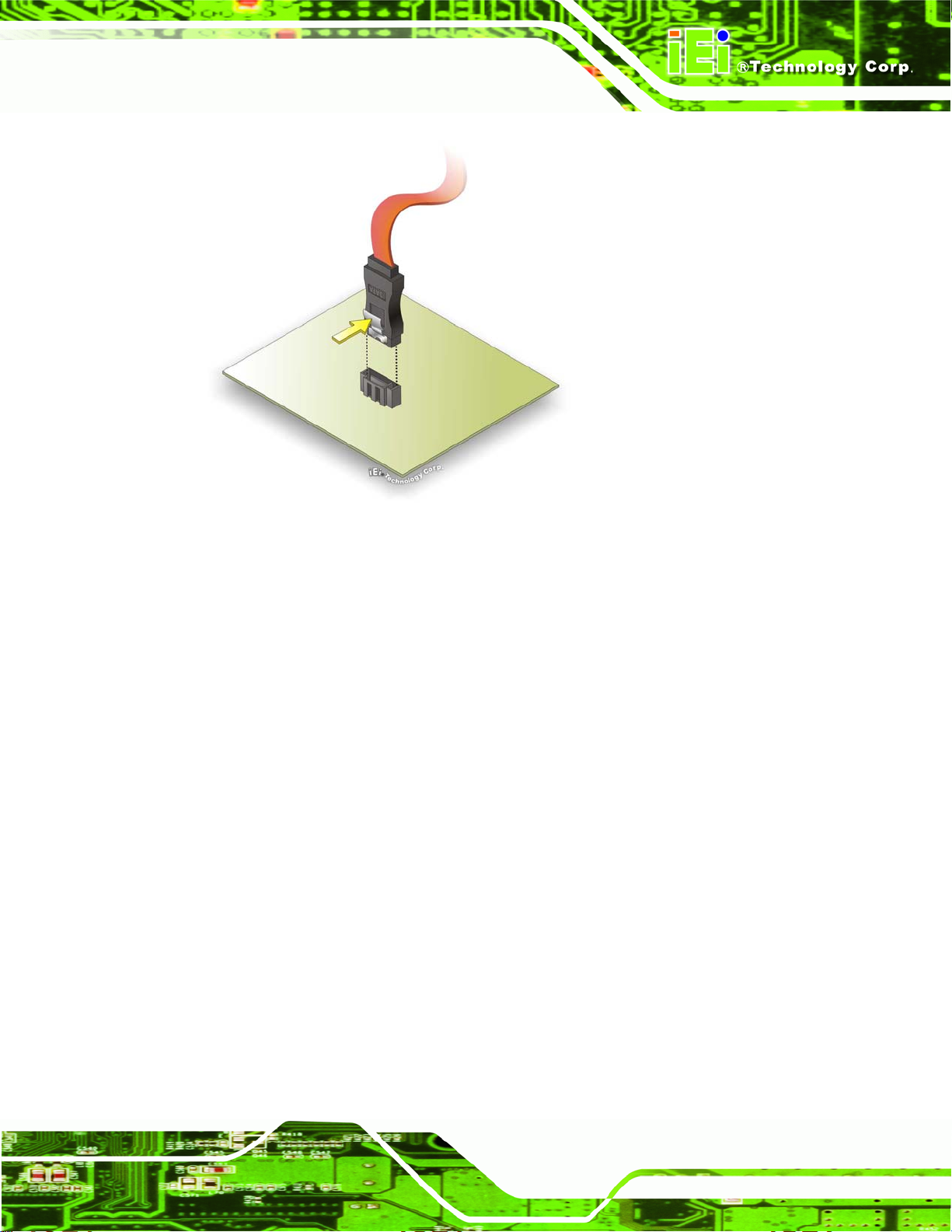
4.5.1 SATA Drive Connection
The PCISA-PV-D4251/N4551/D5251 is shipped with three SATA drive cables. To connect
the SATA drives to the connectors, please follow the steps below.
Step 1: Locate the connectors. The locations of the SATA drive connectors are shown
in Chapter 3.
Step 2: Insert the cable connector. Press the clip on the connector at the end of the
SATA ca ble and insert the cable connector into the on-board SATA drive
connector. See
Figure 4-9.
Page 52
Page 66
PCISA-PV-D4251/N4551/D5251 CPU Card
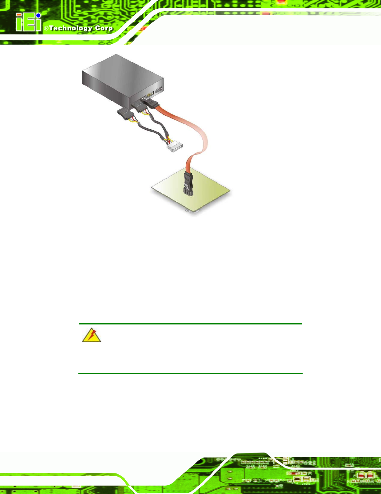
Figure 4-9: SATA Drive Cable Connection
Step 3: Connect the cable to the SATA disk. Connect the connector on the other end
of the cable to the connector at the back of the SATA drive. See
Step 4: Connect the SATA power cable. Connect the SATA power connector to the
back of the SATA drive. See
Figure 4-10.
Figure 4-10.
Page 53
Page 67
PCISA-PV-D4251/N4551/D5251 CPU Card
Figure 4-10: SATA Power Drive Connection
4.5.2 USB Cable (Dual Port) with Slot Bracket
The PCISA-PV-D4251/N4551/D5251 is shipped with a dual port USB 2.0 cable. To
connect the USB cable connector, please follow the steps below.
Step 1: Locate the connectors. The locations of the USB connectors are shown in
Chapter 3.
WARNING:
If the USB pins are not properly aligned, the USB device can burn out.
Step 2: Align the connectors. The cable has two connectors. Correctly align pin 1of
Page 54
the cable connector with pin 1 on the PCISA-PV-D4251/N4551/D5251 USB
connector.
Page 68

PCISA-PV-D4251/N4551/D5251 CPU Card
Step 3: Insert the cable connectors. Once the cable connectors are properly aligned
with the USB connectors on the PCISA-PV-D4251/N4551/D5251, connect the
cable connectors to the on-board connectors. See
Figure 4-11: Dual USB Cable Connection
Figure 4-11.
Step 4: Attach the bracket to the chassis. The USB 2.0 connectors are attached to a
bracket. To secure the bracket to the chassis please refer to the installation
instructions that came with the chassis.Step 0:
4.6 External Peripheral Interface Connection
This section describes connecting devices to the external connectors on the
PCISA-PV-D4251/N4551/D5251.
4.6.1 LAN Connection
There are two external RJ-45 LAN connectors. The RJ-45 connectors enable connection
to an external network. To connect a LAN cable with an RJ-45 connector, please follow
the instructions below.
Page 55
Page 69

Step 1: Locate the RJ-45 connectors. The locations of the RJ45 connecto rs are
shown in Chapter 3.
Step 2: Align the connectors. Align the RJ-45 connector on the LAN cable with one of
PCISA-PV-D4251/N4551/D5251 CPU Card
the RJ-45 connectors on the PCISA-PV-D4251/N4551/D5251. See
Figure 4-12: LAN Connection
Step 3: Insert the LAN cable RJ-45 connector. Once aligned, gently insert the LAN
Figure 4-12.
cable RJ-45 connector into the on-board RJ-45 connector. Step 0:
4.6.2 USB Device Connection
There are two external USB 2.0 connectors. To connect a USB 2.0 or USB 1.1 device,
please follow the instructions below.
Step 1: Located the USB connectors. The locations of the USB connect ors are shown
in Chapter 3.
Step 2: Align the connectors. Align the USB device connector with one of the
connectors on the PCISA-PV-D4251/N4551/D5251. See
Page 56
Figure 4-13.
Page 70

PCISA-PV-D4251/N4551/D5251 CPU Card
Figure 4-13: USB Device Connection
Step 3: Insert the device connector. Once aligned, gently insert the USB device
connector into the on-board connector. Step 0:
4.6.3 VGA Monitor Connection
The PCISA-PV-D4251/N4551/D5251 has a single female DB-15 connector on the
external peripheral interface panel. The DB-15 connector is connected to a CRT or VGA
monitor. To connect a monitor to the PCISA-PV-D4251/N4551/D5251, please follow the
instructions below.
Step 1: Locate the female DB-15 connector. The location of the female DB-15
connector is shown in Chapter 3.
Step 2: Align the VGA connector. Align the male DB-15 connector on the VGA screen
cable with the female DB-15 connector on the external peripheral interface.
Step 3: Insert the VGA connector. Once the conne ctors are prop erly aligned with the
insert the male connector from the VGA screen into the female connector on the
PCISA-PV-D4251/N4551/D5251. See
Figure 4-14.
Page 57
Page 71

Figure 4-14: VGA Connector
Step 4: Secure the connector. Secure the DB-15 VGA connector from the VGA
PCISA-PV-D4251/N4551/D5251 CPU Card
monitor to the external interface by tightening the two retention screws on either
side of the connector. Step 0:
4.7 Software Installation
All the drivers for the PCISA-PV-D4251/N4551/D5251 are on the CD that came with the
system. To install the drivers, please follow the steps below.
Step 1: Insert the CD into a CD drive connected to the system.
NOTE:
If the installation program doesn't start automatically:
Click "Start->My Computer->CD Drive->autorun.exe"
Step 2: The driver main menu appears.
Page 58
Step 3: Click PCISA-PV-D4251/ N4551/D5251.
Step 4: A new screen with a list of available drivers a ppears.
Step 5: Install all of the necessary drivers in this menu. Step 0:
Page 72

PCISA-PV-D4251/N4551/D5251 CPU Card
Chapter
5
5 BIOS
Page 59
Page 73

5.1 Introduction
The BIOS is programmed onto the BIOS chip. The BIOS setup program allows changes to
certain system settings. This chapter outlines the options that can be changed.
5.1.1 Starting Setup
The UEFI BIOS is activated when the computer is turned on. The setup program can be
activated in one of two ways.
PCISA-PV-D4251/N4551/D5251 CPU Card
1. Press the
2. Press the
the screen. 0.
If the message disappears before the F2 key is pressed, restart the computer and try
again.
F2 key as soon as the system is turned on or
F2 key when the “Press F2 to enter SETUP” message appears on
5.1.2 Using Setup
Use the arrow keys to highlight items, press ENTER to select, use the PageUp and
PageDown keys to change entries, press F1 for help and press E
keys are shown in.
Key Function
Up arrow Move to previous item
Down arrow Move to next item
Left arrow Move to the item on the left hand side
SC to quit. Navigation
Page 60
Right arrow Move to the item on the right hand side
F1 key General help, only for Status Page Setup Menu and Option
Page Setup Menu
F2 key Load previous values.
F3 key Load optimized defaults
Page 74

PCISA-PV-D4251/N4551/D5251 CPU Card
Key Function
F4 key Save all the CMOS changes
Esc key Main Menu – Quit and not save changes into CMOS
Status Page Setup Menu and Option Page Setup Menu --
Exit current page and return to Main Menu
Table 5-1: BIOS Navigation Keys
5.1.3 Getting Help
When F1 is pressed a small help window describing the appropriate keys to use and the
possible selections for the highlighted item appears. To exit the Help Window press E
the F1 key again.
5.1.4 Unable to Reboot After Configuration Changes
If the computer cannot boot after changes to the system configuration is made, CMOS
defaults. Use the jumper described in Chapter 4.
5.1.5 BIOS Menu Bar
The menu bar on top of the BIOS screen has the following main items:
Main – Changes the basic system configuration.
Advanced – Changes the advanced system settings.
Chipset – Changes the chipset settings.
Boot – Changes the system boot configuration.
Security – Sets User and Supervisor Passwords.
Save & Exit – Selects exit options and loads default settings
SC or
The following sections completely describe the configuration options found in the menu
items at the top of the BIOS screen and listed above.
Page 61
Page 75

S
PCISA-PV-D4251/N4551/D5251 CPU Card
5.2 Main
The Main BIOS menu (BIOS Menu 1) appears when the BIOS Setup program is entered.
The Main menu gives an overview of the basic system information.
Aptio Setup Utility – Copyright (C) 2010 American Megatrends, Inc.
Main Advanced Chipset Boot Security Save & Exit
BIOS Information
BIOS Vendor American Megatrends
Core Version 4.6.4.0 0.20
Compliency UEFI 2.0
Project Version SA12AR11.ROM
Build Date 08/18/2010 09:00:13
System Date [Tue 05/06/2008]
System Time [14:20:27]
Access Level Administrator
Version 2.01.1204. Copyright (C) 2010 American Megatrends, Inc.
et the Time. Use Tab to
switch between Time
elements.
----------------------
ÅÆ
: Select Screen
↑ ↓: Select Item
Enter Select
F1 General Help
F2 Previous Values
F3 Optimized Defaults
F4 Save
ESC Exit
BIOS Menu 1: Main
Î BIOS Information
The BIOS Information lists a brief summary of the BIOS. The fields in BIOS Information
cannot be changed. The items shown in the system overview include:
BIOS Vendor: Installed BIOS vendor
Core Version: Current BIOS version
Project Version: the bo ard version
Build Date: Date the current BIOS version was made
The System Overview field also has two user configurable fields:
Î System Date [xx/xx/xx]
Use the System Date option to set the system date. Manually enter the day, month and
year.
Page 62
Page 76

PCISA-PV-D4251/N4551/D5251 CPU Card
Î System Time [xx:xx:xx]
Use the System Time option to set the system time. Manually enter the hours, minutes
and seconds.
5.3 Advanced
Use the Advanced menu (BIOS Menu 2) to configure the CPU and peripheral devices
through the following sub-menus:
WARNING!
Setting the wrong values in the sections below may cause the system
to malfunction. Make sure that the settings made are compatible with
the hardware.
Aptio Setup Utility – Copyright (C) 2010 American Megatrends, Inc.
Main Advanced Chipset Boot Security Save & Exit
> Trusted Computing
> CPU Configuration
> SATA Configuration
> USB Configuration
> Super IO Configuration
> H/M Monitor
> Serial Port Console Redirection
Version 2.01.1204. Copyright (C) 2010 American Megatrends, Inc.
BIOS Menu 2: Advanced
System ACPI Parameters
----------------------
ÅÆ
↑ ↓: Select Item
Enter Select
F1 General Help
F2 Previous Values
F3 Optimized
Defaults
F4 Save
ESC Exit
5.3.1 Trusted Computing
: Select Screen
Use the Trusted Computing menu (BIOS Menu 3) to configure settings related to the
Trusted Computing Group (TCG) Trusted Platform Module (TPM).
Page 63
Page 77

E
Aptio Setup Utility – Copyright (C) 2010 American Megatrends, Inc.
Advanced
TPM Configuration
TPM SUPPORT [Disable]
Current TPM Status Information
NO TPM Hardware
Version 2.01.1204. Copyright (C) 2010 American Megatrends, Inc.
BIOS Menu 3: TPM Configuration
PCISA-PV-D4251/N4551/D5251 CPU Card
nables or Disables TPM
support. O.S. will not
show TPM. Reset of
platform is required.
----------------------
ÅÆ
: Select Screen
↑ ↓: Select Item
Enter Select
F1 General Help
F2 Previous Values
F3 Optimized
Defaults
F4 Save
ESC Exit
Î TPM Support [Disable]
Use the TPM Support option to configure support for the TPM.
Î
Disable DEFAULT
Î
Enable
TPM support is disabled.
TPM support is enabled.
5.3.2 CPU Configuration
Use the CPU Configuration menu (BIOS Menu 4) to view detailed CPU specifications
and configure the CPU.
Page 64
Page 78

PCISA-PV-D4251/N4551/D5251 CPU Card
Aptio Setup Utility – Copyright (C) 2010 American Megatrends, Inc.
Advanced
CPU Configuration
Processor Type Intel(R) Atom(TM) CPU
EMT64 Supported
Processor Speed 1834 MHz
System Bus Speed 667 MHz
Ratio Status 11
Actual Ratio 11
Processor Stepping 106ca
Microcode Revision 263
L1 Cache RAM 56 k
L2 Cache RAM 512 k
Processor Core Single
Hyper-Threading Supported
Version 2.01.1204. Copyright (C) 2010 American Megatrends, Inc.
BIOS Menu 4: CPU Configuration
----------------------
ÅÆ
: Select Screen
↑ ↓: Select Item
Enter Select
F1 General Help
F2 Previous Values
F3 Optimized
Defaults
F4 Save
ESC Exit
The CPU Configuration menu (
Processor Type: Lists the brand name of the CPU being used
EMT64: Indicates if the EM64T is supported by the CPU.
Processor Speed: Lists the CPU processing speed
System Bus: Lists the system bus
Ratio Status: List the maximum FSB divisor
Actual Ratio: Lists current FSB divisor
Processor Stepping: Lists the CPU processing stepping
Microcode Revision: Lists the microcode revision
L1 Cache RAM: Lists the CPU L1 cache size
L2 Cache RAM: Lists the CPU L2 cache size
Processor Core: Lists the number of the processor core
Hyper-Threading: Indicates if the Intel Hyper-Threading Technology is
supported by the CPU.
BIOS Menu 4) lists the following CPU details:
Page 65
Page 79

PCISA-PV-D4251/N4551/D5251 CPU Card
5.3.3 SATA Configuration
Use the SATA Configuration menu (BIOS Menu 5) to change and/or set the
configuration of the SATA devices installed in the system.
Aptio Setup Utility – Copyright (C) 2010 American Megatrends, Inc.
Advanced
PATA Master Not Present
PATA Slave Not Present
SATA Port0 Not Present
SATA Port1 Not Present
SATA Port2 Not Present
SATA Port3 Not Present
ATA/IDE Configuration [Enhanced]
Configure SATA as [IDE]
Version 2.01.1204. Copyright (C) 2010 American Megatrends, Inc.
Select ATA/IDE
Configuration.
---------------------
ÅÆ
: Select Screen
↑ ↓: Select Item
Enter Select
F1 General Help
F2 Previous Values
F3 Optimized
Defaults
F4 Save
ESC Exit
BIOS Menu 5: IDE Configuration
Î ATA/IDE Configurations [Enhanced]
Use the ATA/IDE Configurations option to configure the ATA/IDE controller.
Î
Disabled
Î
Compatible
Î
Enhanced DEFAULT
Disables the on-board ATA/IDE controller.
Configures the on-board ATA/IDE controller to be in
compatible mode. In this mode, a SATA channel will
replace one of the IDE channels. This mode supports
up to 4 storage devices.
Configures the on-board ATA/IDE controller to be in
Enhanced mode. In this mode, IDE channels and SATA
channels are separated. This mode supports up to 6
storage devices. Some legacy OS do not support this
mode.
Page 66
Page 80

d
PCISA-PV-D4251/N4551/D5251 CPU Card
Î Configure SATA as [IDE]
Use the Configure SATA as option to configure SATA devices as normal IDE devices.
Î
IDE DEFAULT
Î
AHCI
Configures SATA devices as normal IDE device.
Configures SATA devices as AHCI device.
5.3.4 USB Configuration
Use the USB Configuration menu (BIOS Menu 6) to read USB configuration information
and configure the USB settings.
Aptio Setup Utility – Copyright (C) 2010 American Megatrends, Inc.
Advanced
USB Configuration
USB Devices:
1 Keyboard, 2 Hubs
Legacy USB Support [Enabled]
Version 2.01.1204. Copyright (C) 2010 American Megatrends, Inc.
Enables Legacy USB
support. AUTO option
isables legacy support
if no USB devices are
connected. DISABLE
option will keep USB
devices available only
for EFI applications.
---------------------
ÅÆ
: Select Screen
↑ ↓: Select Item
Enter Select
F1 General Help
F2 Previous Values
F3 Optimized
Defaults
F4 Save
ESC Exit
BIOS Menu 6: USB Configuration
Î USB Devices
The USB Devices Enabled field lists the USB devices that are enabled on the system
Page 67
Page 81

S
Î Legacy USB Support [Enabled]
Use the Legacy USB Support BIOS option to enable USB mouse and USB keyboard
support. Normally if this option is not enabled, any attached USB mouse or USB keyboard
does not become available until a USB compatible operating system is fully booted with all
USB drivers loaded. When this option is enabled, any attached USB mouse or USB
keyboard can control the system even when there is no USB driver loaded onto the
system.
PCISA-PV-D4251/N4551/D5251 CPU Card
Î
Enabled DEFAULT
Î
Disabled
Î
Auto
Legacy USB support enabled
Legacy USB support disabled
Legacy USB support disabled if no USB devices are
connected
5.3.5 Super IO Configuration
Use the Super IO Configuration menu (BIOS Menu 7) to set or change the
configurations for the FDD controllers, parallel ports and serial ports.
Aptio Setup Utility – Copyright (C) 2010 American Megatrends, Inc.
Advanced
Super IO Configuration
Super IO Chip Finteck F81865
> Floppy Disk Controller Configuration
> Serial Port 0 Configuration
> Serial Port 1 Configuration
> Serial Port 2 Configuration
> Serial Port 3 Configuration
> IrDA Configuration
> Parallel Port Configuration
Version 2.01.1204. Copyright (C) 2010 American Megatrends, Inc.
et Parameters of Serial
Port 0 (COMA)
---------------------
ÅÆ
: Select Screen
↑ ↓: Select Item
Enter Select
F1 General Help
F2 Previous Values
F3 Optimized
Defaults
F4 Save
ESC Exit
BIOS Menu 7: Super IO Configuration
Page 68
Page 82

E
PCISA-PV-D4251/N4551/D5251 CPU Card
5.3.5.1 Floppy Disk Controller Configuration
Use the Serial Port n Configuration menu (BIOS Menu 9) to configure the serial port n.
Aptio Setup Utility – Copyright (C) 2010 American Megatrends, Inc.
Advanced
Floppy Disk Controller Configuration
Floppy Disk Controller [Enabled]
Device Settings Reset Required
Version 2.01.1204. Copyright (C) 2010 American Megatrends, Inc.
nable or Disable Floppy
Disk Controller
---------------------
ÅÆ
: Select Screen
↑ ↓: Select Item
Enter Select
F1 General Help
F2 Previous Values
F3 Optimized
Defaults
F4 Save
ESC Exit
BIOS Menu 8: Floppy Disk Controller Configuration Menu
Î Floppy Disk Controller [Enabled]
Use the Floppy Disk Controller option to enable or disable the floppy disk controller.
Î
Disabled
Î
Enabled DEFAULT
Disable the floppy disk controller
Enable the floppy disk controller
Page 69
Page 83

E
PCISA-PV-D4251/N4551/D5251 CPU Card
5.3.5.2 Serial Port n Configuration
Use the Serial Port n Configuration menu (BIOS Menu 9) to configure the serial port n.
Aptio Setup Utility – Copyright (C) 2010 American Megatrends, Inc.
Advanced
Serial Port 0 Configuration
Serial Port [Enabled]
Device Settings IO=3F8h; IRQ=4
Change Settings [Auto]
Version 2.01.1204. Copyright (C) 2010 American Megatrends, Inc.
nable or Disable Serial
Port (COM)
---------------------
ÅÆ
: Select Screen
↑ ↓: Select Item
Enter Select
F1 General Help
F2 Previous Values
F3 Optimized
Defaults
F4 Save
ESC Exit
BIOS Menu 9: Serial Port n Configuration Menu
5.3.5.2.1 Serial Port 0 Configuration
Î Serial Port [Enabled]
Use the Serial Port option to enable or disable the serial port.
Î
Disabled
Î
Enabled DEFAULT
Î Change Settings [Auto]
Use the Change Settings option to change the serial port IO port address and interrupt
address.
Î
Auto DEFAULT
Disable the serial port
Enable the serial port
The serial port IO port address and interrupt address
are automatically detected.
Î
IO=3F8h;
IRQ=4
Page 70
Serial Port I/O port address is 3F8h and the interrupt
address is IRQ4
Page 84

PCISA-PV-D4251/N4551/D5251 CPU Card
Î
IO=3F8h;
IRQ=3, 4
Î
IO=2F8h;
IRQ=3, 4
5.3.5.2.2 Serial Port 1 Configuration
Î Serial Port [Enabled]
Use the Serial Port option to enable or disable the serial port.
Î
Disabled
Î
Enabled DEFAULT
Î Change Settings [Auto]
Use the Change Settings option to change the serial port IO port address and interrupt
Serial Port I/O port address is 3F8h and the interrupt
address is IRQ3 and IRQ4
Serial Port I/O port address is 2F8h and the interrupt
address is IRQ3 and IRQ4
Disable the serial port
Enable the serial port
address.
Î
Auto DEFAULT
Î
IO=2F8h;
IRQ=3
Î
IO=3F8h;
IRQ=3, 4
Î
IO=2F8h;
IRQ=3, 4
5.3.5.2.3 Serial Port 2 Configuration
Î Serial Port [Enabled]
Use the Serial Port option to enable or disable the serial port.
The serial port IO port address and interrupt address
are automatically detected.
Serial Port I/O port address is 2F8h and the interrupt
address is IRQ3
Serial Port I/O port address is 3F8h and the interrupt
address is IRQ3 and IRQ4
Serial Port I/O port address is 2F8h and the interrupt
address is IRQ3 and IRQ4
Î
Disabled
Disable the serial port
Page 71
Page 85

PCISA-PV-D4251/N4551/D5251 CPU Card
Î
Enabled DEFAULT
Î Change Settings [Auto]
Use the Change Settings option to change the serial port IO port address and interrupt
address.
Î
Auto DEFAULT
Î
Î
Î
IO=3E8h;
IRQ=11
IO=3E8h;
IRQ=10, 11
IO=2E8h;
IRQ=10, 11
Enable the serial port
The serial port IO port address and interrupt address
are automatically detected.
Serial Port I/O port address is 3E8h and the interrupt
address is IRQ11
Serial Port I/O port address is 3E8h and the interrupt
address is IRQ10, 11
Serial Port I/O port address is 2E8h and the interrupt
address is IRQ10, 11
5.3.5.2.4 Serial Port 3 Configuration
Î Serial Port [Enabled]
Use the Serial Port option to enable or disable the serial port.
Î
Disabled
Î
Enabled DEFAULT
Î Change Settings [Auto]
Use the Change Settings option to change the serial port IO port address and interrupt
address.
Î
Auto DEFAULT
Disable the serial port
Enable the serial port
The serial port IO port address and interrupt address
are automatically detected.
Page 72
Page 86

PCISA-PV-D4251/N4551/D5251 CPU Card
Î
Î
Î
IO=2E8h;
IRQ=10
IO=3E8h;
IRQ=10, 11
IO=2E8h;
IRQ=10, 11
Serial Port I/O port address is 2E8h and the interrupt
address is IRQ10
Serial Port I/O port address is 3E8h and the interrupt
address is IRQ10, 11
Serial Port I/O port address is 2E8h and the interrupt
address is IRQ10, 11
5.3.5.3 IrDA Configuration
Use the IrDA Configuration menu (BIOS Menu 9) to configure the serial port n.
Aptio Setup Utility – Copyright (C) 2010 American Megatrends, Inc.
Advanced
IrDA Configuration
IrDA [Enabled]
Device Settings Reset Required
Enable or Disable IrDA
---------------------
ÅÆ
: Select Screen
↑ ↓: Select Item
Enter Select
F1 General Help
F2 Previous Values
F3 Optimized
Defaults
F4 Save
ESC Exit
Version 2.01.1204. Copyright (C) 2010 American Megatrends, Inc.
BIOS Menu 10: IrDA Configuration Menu
Î IrDA [Enabled]
Use the IrDA option to enable or disable the infrared function.
Î
Î
Disabled
Enabled DEFAULT
Disable the infrared function
Enable the infrared function
Page 73
Page 87

C
PCISA-PV-D4251/N4551/D5251 CPU Card
5.3.5.4 Parallel Port Configuration
Use the Parallel Port Configuration menu (BIOS Menu 9) to configure the serial port n.
Aptio Setup Utility – Copyright (C) 2010 American Megatrends, Inc.
Advanced
Parallel Port Configuration
Parallel Port [Enabled]
Device Settings IO=378h; IRQ=7
Change Settings [Auto]
Device Mode [Printer Mode]
Version 2.01.1204. Copyright (C) 2010 American Megatrends, Inc.
hange the Printer Port
mode
---------------------
ÅÆ
: Select Screen
↑ ↓: Select Item
Enter Select
F1 General Help
F2 Previous Values
F3 Optimized
Defaults
F4 Save
ESC Exit
BIOS Menu 11: Parallel Port Configuration Menu
Î Parallel Port [Enabled]
Use the Parallel Port option to enable or disable the parallel port.
Î
Disabled
Î
Enabled DEFAULT
Î Change Settings [Auto]
Use the Change Settings option to change the parallel port IO port address and interrupt
address.
Î
Auto DEFAULT
Î
IO=378h;
Disable the parallel port
Enable the parallel port
The parallel port IO port address and interrupt
address are automatically detected.
Parallel Port I/O port address is 378h and the
IRQ=7
Î
IO=278h;
IRQ=7
Page 74
interrupt address is IRQ7
Parallel Port I/O port address is 278h and the
interrupt address is IRQ7
Page 88

PCISA-PV-D4251/N4551/D5251 CPU Card
Î
IO=3BCh;
IRQ=7
Î
IO=378h
Î
IO=278h
Î
IO=3BCh
Î Device Mode [Printer Mode]
Use the Device Mode option to select the mode the parallel port operates in.
Configuration options are listed below.
Printer Mode Default
SPP Mode
EPP-1.9 and SPP Mode
EPP-1.7 and SPP Mode
ECP Mode
Parallel Port I/O port address is 3BCh and the
interrupt address is IRQ7
Parallel Port I/O port address is 378h
Parallel Port I/O port address is 278h
Parallel Port I/O port address is 3BCh
ECP and EPP 1.9 Mode
ECP and EPP 1.7 Mode
5.3.6 H/W Monitor
The H/W Monitor menu (BIOS Menu 12) shows the operating temperature, fan speeds
and system voltages.
Page 75
Page 89

Aptio Setup Utility – Copyright (C) 2010 American Megatrends, Inc.
Advanced
PC Health Status
CPU Temperature :+37 C
SYS Temperature :+36 C
CPU FAN Speed :5976 RPM
VCC3C :+3.312 V
V_core :+1.288 V
Vcc :+5.129 V
Vcc12 :+11.968 V
V1_5VDDR :+1.504 V
VSB3V :+3.424 V
VBAT :+3.328 V
CPU Smart Fan control [Auto Mode]
Temperature Bound1 60
Temperature Bound2 50
Temperature Bound3 40
Temperature Bound4 30
Version 2.01.1204. Copyright (C) 2010 American Megatrends, Inc.
PCISA-PV-D4251/N4551/D5251 CPU Card
---------------------
ÅÆ
: Select Screen
↑ ↓: Select Item
Enter Select
F1 General Help
F2 Previous Values
F3 Optimized
Defaults
F4 Save
ESC Exit
BIOS Menu 12: Hardware Health Configuration
Î PC Health Status
The following system parameters and values are shown. The system parameters that are
monitored are:
System Temperatures:
o CPU Temperature
o System Temperature
Fan Speeds:
o CPU Fan Speed
Voltages:
o V_core
o Vcc
o Vcc12
o V1_5VDDR
Page 76
o VSB3V
o VBAT
Page 90

PCISA-PV-D4251/N4551/D5251 CPU Card
Î CPU Smart Fan control [Auto Mode]
Use the CPU Smart Fan control option to configure the CPU fan.
Î
Auto Mode
Î
Manual Mode
The fan adjusts its speed using these settings:
Temperature Bound 1
Temperature Bound 2
Temperature Bound 3
Temperature Bound 4
The fan spins at the speed set in:
Manual Duty Cycle Setting
5.3.7 Serial Port Console Redirection
The Serial Port Console Redirection menu (BIOS Menu 13) allows the console
redirection options to be configured. Console redirection allows users to maintain a
system remotely by re-directing keyboard input and text output through the serial port.
Aptio Setup Utility – Copyright (C) 2010 American Megatrends, Inc.
Advanced
COM0
Console Redirection [Disabled]
> Console Redirection Settings
COM1
Console Redirection [Disabled]
> Console Redirection Settings
COM2
Console Redirection [Disabled]
> Console Redirection Settings
COM3
Console Redirection [Disabled]
> Console Redirection Settings
Version 2.01.1204. Copyright (C) 2010 American Megatrends, Inc.
Console Redirection
Enable/Disable
---------------------
ÅÆ
: Select Screen
↑ ↓: Select Item
Enter Select
F1 General Help
F2 Previous Values
F3 Optimized
Defaults
F4 Save
ESC Exit
BIOS Menu 13: Serial Port Console Redirection
Î Console Redirection [Disabled]
Use Console Redirection option to enable or disable the console redirection fun ction.
Page 77
Page 91

PCISA-PV-D4251/N4551/D5251 CPU Card
Î
Disabled DEFAULT
Î
Enabled
Disabled the console redirection function
Enabled the console redirection function
5.4 Chipset
Use the Chipset menu (BIOS Menu 14) to access the Northbridge and Southbridge
configuration menus
WARNING!
Setting the wrong values for the Chipset BIOS selections in the Chipset
BIOS menu may cause the system to malfunction.
Aptio Setup Utility – Copyright (C) 2010 American Megatrends, Inc.
Main Advanced Chipset Boot Security Save & Exit
> Host Bridge
> South Bridge
> Intel IGD SWSCI OpRegion
North Bridge Parameters
---------------------
ÅÆ
↑ ↓: Select Item
Enter Select
F1 General Help
F2 Previous Values
F3 Optimized
Defaults
F4 Save
ESC Exit
: Select Screen
Page 78
Version 2.01.1204. Copyright (C) 2010 American Megatrends, Inc.
BIOS Menu 14: Chipset
Page 92

c
PCISA-PV-D4251/N4551/D5251 CPU Card
5.4.1 Host Bridge Configuration
Use the Host Bridge Configuration menu (BIOS Menu 15) to configure the Northbridge
chipset.
Aptio Setup Utility – Copyright (C) 2010 American Megatrends, Inc.
Chipset
> OnChip VGA Configuration
Initate Graphic Adapter [IGD]
******* Memory Information *******
Memory Frequency 667 Mhz
Total Memory 1024 MB
DIMM#0 1024 MB
DIMM#1 Not Present
Version 2.01.1204. Copyright (C) 2010 American Megatrends, Inc.
Select which graphics
ontroller to use as the
primary boot device.
---------------------
ÅÆ
: Select Screen
↑ ↓: Select Item
Enter Select
F1 General Help
F2 Previous Values
F3 Optimized
Defaults
F4 Save
ESC Exit
BIOS Menu 15: Host Bridge Chipset Configuration
Î Initiate Graphics Adapter [IGD]
Use the Initiate Graphics Adapter option to select the graphics controller used as the
primary boot device. Select either an integrated graphics controller (IGD) or a combination
of PCI graphics controller, a PCI express (PEG) controller or an IGD. Configuration
options are listed below:
IGD
PCI/IGD
DEFAULT
Page 79
Page 93

PCISA-PV-D4251/N4551/D5251 CPU Card
5.4.1.1 OnChip VGA Configuration
Use the OnChip VGA Configuration menu (BIOS Menu 15) to configure the OnChip
VGA.
Aptio Setup Utility – Copyright (C) 2010 American Megatrends, Inc.
Chipset
OnChip VGA Configuration
Share Memory Size [8 MB]
Multi-Monitor Support [Enabled]
Version 2.01.1204. Copyright (C) 2010 American Megatrends, Inc.
Select Share Memory
Size.
---------------------
ÅÆ
: Select Screen
↑ ↓: Select Item
Enter Select
F1 General Help
F2 Previous Values
F3 Optimized
Defaults
F4 Save
ESC Exit
BIOS Menu 16: OnChip VGA Configuration
Î Share Memory Size [8 MB]
Use the Share Memory Size option to set the amount of system memory allocated to the
integrated graphics processor when the system boots. The system memory allocated can
then only be used as graphics memory, and is no longer available to applications or the
operating system. Configuration options are listed below:
Disabled
1 MB
8 MB Default
Î Multi-Monitor Support [Enabled]
Use Multi-Monitor Support option to enable or disable the multi-monitor function.
Page 80
Page 94

PCISA-PV-D4251/N4551/D5251 CPU Card
Î
Disabled
Î
Enabled DEFAULT
Disabled the multi-monitor function
Enabled the multi-monitor function
5.4.2 South Bridge Configuration
Use the South Bridge Configuration menu (BIOS Menu 17) to configure the
Southbridge chipset.
Aptio Setup Utility – Copyright (C) 2010 American Megatrends, Inc.
Chipset
Auto Power Button Function [Enabled]
HD Audio Controller [Enabled]
USB Function [Enabled]
USB 2.0(EHCI) Support [Enabled]
Set Spread Spectrum function [Disabled]
HD Audio Controller
---------------------
ÅÆ
: Select Screen
↑ ↓: Select Item
Enter Select
F1 General Help
F2 Previous Values
F3 Optimized
Defaults
F4 Save
ESC Exit
Version 2.01.1204. Copyright (C) 2010 American Megatrends, Inc.
BIOS Menu 17:South Bridge Chipset Configuration
Î HD Audio Controller [Enabled]
Use the HD Audio Controller option to enable or disable the High Definition Audio
controller.
Î
Enabled DEFAULT
Î
Disabled
Î USB Function [Enabled]
Use the USB Function BIOS option to enable or disable USB function support.
Î
Disabled
The onboard High Definition Audio controller
automatically detected and enabled
The onboard High Definition Audio controller is disabled
USB function support disabled
Page 81
Page 95

PCISA-PV-D4251/N4551/D5251 CPU Card
Î
Enabled DEFAULT
Î USB 2.0 (EHCI) Support [Enabled]
Use the USB 2.0 (EHCI) Support BIOS option to enable or disable USB 2.0 support.
Î
Enabled DEFAULT
Î
Disabled
Î Set Spread Spectrum Function [Disabled]
The Set Spread Spectrum Function option can help to improve CPU EMI issues.
Î
Disabled DEFAULT
Î
Enabled
USB function support enabled
USB 2.0 (EHCI) support enabled
USB 2.0 (EHCI) support disabled
The spread spectrum mode is disabled
The spread spectrum mode is enabled
5.4.3 Intel IGD SWSCI OpRegion
Use the Intel IGD SWSCI OpRegion menu to configure the video device connected to the
system.
Aptio Setup Utility – Copyright (C) 2010 American Megatrends, Inc.
Chipset
Intel IGD SWSCI OpRegion Configuration
DVMT Mode Select [DVMT Mode]
DVMT/Fixed Memory [256 MB]
IGD - Boot Type [VBIOS Default]
LCD Panel Type [Select by Panel ID]
Panel ID Resolution 1024x768 18bit
Version 2.01.1204. Copyright (C) 2010 American Megatrends, Inc.
BIOS Menu 18:South Bridge Chipset Configuration
Select DVMT Mode/Fixed
Mode
---------------------
ÅÆ
: Select Screen
↑ ↓: Select Item
Enter Select
F1 General Help
F2 Previous Values
F3 Optimized
Defaults
F4 Save
ESC Exit
Page 82
Page 96

PCISA-PV-D4251/N4551/D5251 CPU Card
Î DVMT Mode Select [DVMT Mode]
Use the DVMT Mode Select option to select the Intel Dynamic Video Memory Technology
(DVMT) operating mode.
Î
Fixed
Mode
Î
DVMT
Mode
Î DVMT/FIXED Memory [256 MB]
Use the DVMT/FIXED Memory option to specify the maximum amount of memory that
can be allocated as graphics memory. Configuration options are listed below.
128 MB
256 MB Default
Maximum
Î IGD - Boot Type [VBIOS Default]
Use the IGD - Boot Type option to select the display device used by the system when it
boots. Configuration options are listed below.
DEFAULT
A fixed portion of graphics memory is reserved as
graphics memory.
Graphics memory is dynamically allocated according
to the system and graphics needs.
VBIOS Default
CRT
LFP
CRT + LFP
Î LCD Panel Type [Select by Panel ID]
Use the LCD Panel Type option to select the type of flat panel connected to the system.
Configuration options are listed below.
Select by Panel ID D
640x480 18bit
800x480 18bit
800x600 18bit
DEFAULT
EFAULT
Page 83
Page 97

1024x768 18bit
1280x1024 18bit
1366x768 18bit
1280x800 18bit
1280x600 18bit
PCISA-PV-D4251/N4551/D5251 CPU Card
5.5 Boot
Use the Boot menu (BIOS Menu 19) to configure system boot options.
Aptio Setup Utility – Copyright (C) 2010 American Megatrends, Inc.
Main Advanced Chipset Boot Security Save & Exit
Boot Configuration
Boot NumLock State [On]
Quiet Boot [Enabled]
Fast Boot [Disabled]
Launch PXE OpROM [Disabled]
Boot Option Priorities
Version 2.01.1204. Copyright (C) 2010 American Megatrends, Inc.
Select the keyboard
NumLock state
---------------------
ÅÆ
↑ ↓: Select Item
Enter Select
F1 General Help
F2 Previous Values
F3 Optimized
Defaults
F4 Save
ESC Exit
: Select Screen
BIOS Menu 19: Boot
Î Bootup NumLock State [On]
Use the Bootup NumLock State BIOS option to specify if the number lock setting must
be modified during boot up.
Î
On DEFAULT
Page 84
Allows the Number Lock on the keyboard to be
enabled automatically when the computer system
boots up. This allows the immediate use of the
10-key numeric keypad located on the right side of
the keyboard. To confirm this, the Number Lock LED
light on the keyboard is lit.
Page 98

PCISA-PV-D4251/N4551/D5251 CPU Card
Î
Off
Î Quiet Boot [Enabled]
Use the Quiet Boot BIOS option to select the screen display when the system boots.
Î
Disabled
Î
Enabled DEFAULT
Î Fast Boot [Disabled]
Use the Fast Boot option to enable or disable boot with initialization of a minimal set of
Does not enable the keyboard Number Lock
automatically. To use the 10-keys on the keyboard,
press the Number Lock key located on the upper
left-hand corner of the 10-key pad. The Number
Lock LED on the keyboard lights up when the
Number Lock is engaged.
Normal POST messages displayed
OEM Logo displayed instead of POST messages
devices required to launch active boot option. It has no effect for BBS boot options.
Î
Disabled DEFAULT
Î
Enabled
Î Launch PXE OpROM [Disabled]
Use the Launch PXE OpROM option to enable or disable boot option for legacy network
devices.
Î
Disabled DEFAULT
Î
Enabled
Disable fast boot.
Enable fast boot
Ignore all PXE Option ROMs
Load PXE Option ROMs.
Page 85
Page 99

S
PCISA-PV-D4251/N4551/D5251 CPU Card
5.6 Security
Use the Security menu (BIOS Menu 20) to set system and user passwords.
Aptio Setup Utility – Copyright (C) 2010 American Megatrends, Inc.
Main Advanced Chipset Boot Security Save & Exit
Password Description
If ONLY the Administrator’s password is set,
then this only limits access to Setup and is
only asked for when entering Setup
If ONLY the User’s password is set, then this
is a power on password and must be entered to
boot or enter Setup. In Setup the User will
have Administrator rights.
Administrator Password
User Password
Version 2.01.1204. Copyright (C) 2010 American Megatrends, Inc.
Password
---------------------
ÅÆ
↑ ↓: Select Item
Enter Select
F1 General Help
F2 Previous Values
F3 Optimized
Defaults
F4 Save
ESC Exit
et Setup Administrator
: Select Screen
BIOS Menu 20: Security
Î Administrator Password
Use the Administrator Password to set or change a administrator password.
Î User Password
Use the User Password to set or change a user password.
Page 86
Page 100

E
PCISA-PV-D4251/N4551/D5251 CPU Card
5.7 Exit
Use the Exit menu (BIOS Menu 21) to load default BIOS values, optimal failsafe values
and to save configuration changes.
Aptio Setup Utility – Copyright (C) 2010 American Megatrends, Inc.
Main Advanced Chipset Boot Security Save & Exit
Save Changes and Reset
Discard Changes and Reset
Restore Defaults
Save as User Defaults
Restore User Defaults
Version 2.01.1204. Copyright (C) 2010 American Megatrends, Inc.
saving the changes.
---------------------
ÅÆ
↑ ↓: Select Item
Enter Select
F1 General Help
F2 Previous Values
F3 Optimized
Defaults
F4 Save
ESC Exit
xit system setup after
: Select Screen
BIOS Menu 21:Exit
Î Save Changes and Reset
Use the Save Changes and Reset option to save the changes made to the BIOS options
and to exit the BIOS configuration setup program.
Î Discard Changes and Reset
Use the Discard Changes and Reset option to exit the system without saving the
changes made to the BIOS configuration setup program.
Î Restore Defaults
Use the Restore Defaults option to load the optimal default values for each of the
parameters on the Setup menus. F3 key can be used for this operation.
Page 87
 Loading...