

Page 1

IQ7 Design Guide
IEI Technology Corp.
IQ7 Design Guide
IQ7 Design Guide for IQ7-US15W and IQ7-DB-MITX
User Manual
Rev. 1.01 – 22 July, 2009
Page i
Page 2

Date Version Changes
22 July, 2009 1.01 Various updates and changes
19 May, 2009 1.00 Initial release
IQ7 Design Guide
Revision
Page ii
Page 3

IQ7 Design Guide
COPYRIGHT NOTICE
The information in this document is subject to change without prior notice in order to
improve reliability, design and function and does not represent a commitment on the part
of the manufacturer.
In no event will the manufacturer be liable for direct, indirect, special, incidental, or
consequential damages arising out of the use or inability to use the product or
documentation, even if advised of the possibility of such damages.
This document contains proprietary information protected by copyright. All rights are
Copyright
reserved. No part of this manual may be reproduced by any mechanical, electronic, or
other means in any form without prior written permission of the manufacturer.
TRADEMARKS
All registered trademarks and product names mentioned herein are used for identification
purposes only and may be trademarks and/or registered trademarks of their respective
owners.
Page iii
Page 4

IQ7 Design Guide
Table of Contents
1 IQ7-US15W INTRODUCTION.................................................................................... 1
1.1 IQ7-US15W .............................................................................................................. 2
1.2 BENEFITS ................................................................................................................... 2
1.3 FEATURES................................................................................................................... 3
1.4 CONNECTORS ............................................................................................................. 3
1.5 DIMENSIONS............................................................................................................... 3
1.6 DATA FLOW................................................................................................................ 5
1.7 TECHNICAL SPECIFICATIONS ...................................................................................... 5
2 IQ7-US15W CONNECTOR PINOUTS....................................................................... 7
2.1 PERIPHERAL INTERFACE CONNECTORS....................................................................... 8
2.2 LAYOUT...................................................................................................................... 8
2.3 CONNECTOR PINOUTS ................................................................................................ 8
2.3.1 QSeven Connector ............................................................................................. 9
2.3.2 IDE Connector................................................................................................. 13
3 IQ7-DB-MITX INTRODUCTION............................................................................. 16
3.1 INTRODUCTION......................................................................................................... 17
3.2 BENEFITS ................................................................................................................. 17
3.3 FEATURES................................................................................................................. 18
3.4 CONNECTORS ........................................................................................................... 19
3.5 DIMENSIONS............................................................................................................. 20
3.6 DATA FLOW.............................................................................................................. 23
3.7 TECHNICAL SPECIFICATIONS .................................................................................... 24
4 IQ7-DB-MITX CONNECTOR PINOUTS................................................................ 26
4.1 PERIPHERAL INTERFACE CONNECTORS..................................................................... 27
4.1.1 Layout .............................................................................................................. 27
4.1.2 Peripheral Interface Connectors ..................................................................... 28
4.1.3 External Interface Panel Connectors............................................................... 29
4.2 INTERNAL PERIPHERAL CONNECTORS ...................................................................... 29
Page iv
Page 5

IQ7 Design Guide
4.2.1 ATX Power Connector ..................................................................................... 29
4.2.2 Backlight Inverter Connector .......................................................................... 30
4.2.3 CompactFlash® Slot........................................................................................ 31
4.2.4 Digital I/O Connector...................................................................................... 32
4.2.5 Fan Connector................................................................................................. 33
4.2.6 Front Panel Connector.................................................................................... 34
4.2.7 IDE Connector................................................................................................. 35
4.2.8 IDE (CPU Module to Baseboard).................................................................... 37
4.2.9 LVDS Connector.............................................................................................. 38
4.2.10 Mini USB Port................................................................................................ 39
4.2.11 PCI Express x1 Slot........................................................................................ 40
4.2.12 PCIe Mini Card Slot ...................................................................................... 41
4.2.13 Power Button ................................................................................................. 43
4.2.14 QSeven Connector ......................................................................................... 43
4.2.15 Reset Button................................................................................................... 48
4.2.16 SATA Drive Connectors................................................................................. 48
4.2.17 SATA Power Connectors................................................................................ 49
4.2.18 SDVO Connector............................................................................................ 50
4.2.19 Serial Port Connectors .................................................................................. 51
4.2.20 TTL Connector............................................................................................... 52
4.2.21 USB Connector .............................................................................................. 53
4.3 EXTERNAL INTERFACE CONNECTORS....................................................................... 55
4.3.1 Audio Connector .............................................................................................. 55
4.3.2 Ethernet Connector.......................................................................................... 56
4.3.3 Keyboard and Mouse Connector..................................................................... 57
4.3.4 Parallel Port Connector .................................................................................. 58
4.3.5 Serial Port Connector...................................................................................... 59
4.3.6 USB Ports......................................................................................................... 60
4.3.7 VGA Connector................................................................................................ 61
4.4 JUMPER SETTINGS .................................................................................................... 62
4.4.1 AT/ATX Mode Selection................................................................................... 63
4.4.2 Clear CMOS Jumper........................................................................................ 64
4.4.3 CompactFlash® Master/Slave Selection......................................................... 65
4.4.4 CompactFlash® Voltage Selection.................................................................. 65
4.4.5 LAN & PCIe Enable/Disable........................................................................... 65
Page v
Page 6

4.4.6 TTL Voltage Selection ...................................................................................... 66
4.4.7 SATA & Graphics Settings............................................................................... 66
4.4.8 TTL Enabled/Disable....................................................................................... 67
5 INSTALLATION ......................................................................................................... 68
5.1 ANTI-STATIC PRECAUTIONS...................................................................................... 69
5.2 INSTALLATION CONSIDERATIONS.............................................................................. 69
5.3 CPU MODULE INSTALLATION .................................................................................. 71
6 BIOS.............................................................................................................................. 73
6.1 INTRODUCTION......................................................................................................... 74
6.1.1 Starting Setup................................................................................................... 74
6.1.2 Using Setup...................................................................................................... 74
6.1.3 Getting Help..................................................................................................... 75
6.1.4 Unable to Reboot After Configuration Changes.............................................. 75
IQ7 Design Guide
6.1.5 BIOS Menu Bar................................................................................................ 75
6.2 MAIN........................................................................................................................ 76
6.3 ADVANCED............................................................................................................... 77
6.3.1 CPU Configuration.......................................................................................... 78
6.3.2 IDE Configuration........................................................................................... 79
6.3.2.1 IDE Master, IDE Slave............................................................................. 80
6.3.3 Super IO Configuration ................................................................................... 84
6.3.4 Hardware Health Configuration...................................................................... 88
6.3.5 AHCI Configuration......................................................................................... 91
6.3.5.1 AHCI Port n.............................................................................................. 92
6.3.6 Intel AMT Configuration.................................................................................. 93
6.3.6.1 ME Subsystem Configuration ................................................................... 94
6.3.7 Remote Access Configuration.......................................................................... 96
6.3.8 USB Configuration........................................................................................... 98
6.3.8.1 USB Mass Storage Device Configuration............................................... 101
6.4 PCI/PNP................................................................................................................. 103
6.5 BOOT...................................................................................................................... 104
6.5.1 Boot Settings Configuration........................................................................... 105
6.5.2 Boot Device Priority...................................................................................... 107
6.5.3 Hard Disk Drives........................................................................................... 108
Page vi
Page 7

IQ7 Design Guide
6.5.4 Removable Drives.......................................................................................... 108
6.5.5 CD/DVD Drives............................................................................................. 109
6.6 SECURITY............................................................................................................... 109
6.7 CHIPSET ..................................................................................................................111
6.7.1 Northbridge Configuration.............................................................................111
6.7.2 Southbridge Configuration .............................................................................113
6.8 EXIT........................................................................................................................114
A BIOS OPTIONS .........................................................................................................116
B TERMINOLOGY...................................................................................................... 120
C HAZARDOUS MATERIALS DISCLOSURE....................................................... 124
C.1 HAZARDOUS MATERIALS DISCLOSURE TABLE FOR IPB PRODUCTS CERTIFIED AS
ROHS COMPLIANT UNDER 2002/95/EC WITHOUT MERCURY ..................................... 125
Page vii
Page 8

IQ7 Design Guide
List of Figures
Figure 1-1: IQ7-US15W IQ7 Design Guide....................................................................................2
Figure 1-2: Connectors ..................................................................................................................3
Figure 1-3: IQ7-US15W Dimensions (mm) ...................................................................................4
Figure 1-4: Data Flow Diagram......................................................................................................5
Figure 2-1: Connector and Jumper Locations.............................................................................8
Figure 2-2: QSeven Connector......................................................................................................9
Figure 2-3: IDE Connector ...........................................................................................................14
Figure 3-1: IQ7-DB-MITX ..............................................................................................................17
Figure 3-2: Top Connectors.........................................................................................................19
Figure 3-3: Rear Panel Connectors.............................................................................................20
Figure 3-4: IQ7-DB-MITX Dimensions (mm)...............................................................................21
Figure 3-5: External Interface Panel Dimensions (mm)............................................................22
Figure 3-6: Data Flow Diagram....................................................................................................23
Figure 4-1: Connector and Jumper Locations...........................................................................27
Figure 4-2: ATX Power Connector Pinout Locations................................................................30
Figure 4-3: Backlight Inverter Connector...................................................................................31
Figure 4-4: CompactFlash® Slot Location.................................................................................32
Figure 4-5: Digital I/O Connector Locations ..............................................................................33
Figure 4-6: Fan Connector Location...........................................................................................34
Figure 4-7: Front Panel Connector Pinout Locations...............................................................35
Figure 4-8: IDE Connector Locations.........................................................................................36
Figure 4-9: CPU Module to Baseboard IDE Connector Location.............................................37
Figure 4-10: LVDS Connector Location......................................................................................38
Figure 4-11: Mini USB Port Location..........................................................................................40
Figure 4-12: PCIe x1 Connector Location..................................................................................41
Figure 4-13: PCIe Mini Card Slot Location.................................................................................42
Figure 4-14: Power Button Location...........................................................................................43
Figure 4-15: QSeven Connector Location..................................................................................44
Figure 4-16: Reset Button Location............................................................................................48
Figure 4-17: SATA Drive Connector Locations.........................................................................49
Page viii
Page 9

IQ7 Design Guide
Figure 4-18: SATA Power Connector Locations .......................................................................49
Figure 4-19: Serial Port Connector Locations...........................................................................51
Figure 4-20: TTL Connector Location.........................................................................................52
Figure 4-21: USB Connector Locations......................................................................................54
Figure 4-22: External Interface Connectors...............................................................................55
Figure 4-23: Audio Connector.....................................................................................................56
Figure 4-24: Ethernet Connector.................................................................................................57
Figure 4-25: PS/2 Connector .......................................................................................................58
Figure 4-26: Parallel Port Connector Location..........................................................................59
Figure 4-27: Serial Port Pinout Locations..................................................................................60
Figure 4-28: VGA Connector .......................................................................................................61
Figure 4–29: Jumpers ..................................................................................................................63
Figure 5-1: Installing the QSeven CPU Module.........................................................................72
Page ix
Page 10

IQ7 Design Guide
List of Tables
Table 1-1: Technical Specifications..............................................................................................6
Table 2-1: Peripheral Interface Connectors.................................................................................8
Table 2-2: QSeven Connector .....................................................................................................13
Table 2-3: IDE Connector.............................................................................................................15
Table 3-1: Technical Specifications............................................................................................25
Table 4-1: Peripheral Interface Connectors...............................................................................28
Table 4-2: Rear Panel Connectors..............................................................................................29
Table 4-3: ATX Power Connector Pinouts .................................................................................30
Table 4-4: Backlight Inverter Connector ....................................................................................31
Table 4-5: Digital I/O Connector Pinouts....................................................................................33
Table 4-6: Fan Connector Pinouts..............................................................................................34
Table 4-7: Front Panel Connector Pinouts.................................................................................35
Table 4-8: IDE Connector Pinouts...............................................................................................37
Table 4-9: CPU Module to Baseboard IDE Pinouts...................................................................38
Table 4-10: LVDS Connector Pinouts.........................................................................................39
Table 4-11: Mini USB Port Pinouts..............................................................................................40
Table 4-12: PCIe x1 Slot Pinouts.................................................................................................41
Table 4-13: PCIe Mini Card Slot Pinouts ....................................................................................43
Table 4-14: QSeven Connector Pinouts.....................................................................................48
Table 4-15: SATA Power Connector Pinouts.............................................................................50
Table 4-16: IDE Connector Pinouts.............................................................................................51
Table 4-17: Serial Port Connector Pinouts ................................................................................52
Table 4-18: TTL Connector Pinouts............................................................................................53
Table 4-19: USB Port Connector Pinouts...................................................................................54
Table 4-20: Audio Connector Pinouts ........................................................................................56
Table 4-21: Ethernet Connector Pinouts....................................................................................56
Table 4-22: Connector LEDs........................................................................................................57
Table 4-23: PS/2 Connectors.......................................................................................................58
Table 4-24: Parallel Port Connector Pinouts .............................................................................59
Table 4-25: Serial Port Pinouts....................................................................................................60
Page x
Page 11

IQ7 Design Guide
Table 4-26: USB Connector Pinouts...........................................................................................61
Table 4-27: VGA Connector Pinouts...........................................................................................61
Table 4-28: Jumpers.....................................................................................................................62
Table 4-29: AT/ATX Mode Selection ...........................................................................................63
Table 4-30: AT/ATX Mode Selection ...........................................................................................64
Table 4-31: Clear CMOS Jumper Settings..................................................................................64
Table 4-32: CompactFlash® Master/Slave Selection................................................................65
Table 4-33: CompactFlash® Voltage Selection.........................................................................65
Table 4-34: LAN & PCIe Enable/Disable.....................................................................................66
Table 4-35: LVDS Voltage Selection...........................................................................................66
Table 4-36: LAN & PCIe Enable/Disable.....................................................................................67
Table 4-37: TTL Enable/Disable...................................................................................................67
Table 6-1: BIOS Navigation Keys................................................................................................75
Page xi
Page 12

IQ7 Design Guide
BIOS Menus
BIOS Menu 1: Main.......................................................................................................................76
BIOS Menu 2: Advanced..............................................................................................................77
BIOS Menu 3: CPU Configuration...............................................................................................78
BIOS Menu 4: IDE Configuration.................................................................................................79
BIOS Menu 5: IDE Master and IDE Slave Configuration...........................................................80
BIOS Menu 6: Super IO Configuration........................................................................................84
BIOS Menu 7: Hardware Health Configuration..........................................................................88
BIOS Menu 8: AHCI Configuration..............................................................................................91
BIOS Menu 9: AHCI Port n Configuration Menu........................................................................92
BIOS Menu 10: Intel AMT Configuration ....................................................................................93
BIOS Menu 11: ME Subsystem Configuration...........................................................................94
BIOS Menu 12: Remote Access Configuration..........................................................................96
BIOS Menu 13: USB Configuration.............................................................................................98
BIOS Menu 14: USB Mass Storage Device Configuration..................................................... 101
BIOS Menu 15: PCI/PnP Configuration.................................................................................... 103
BIOS Menu 16: Boot.................................................................................................................. 104
BIOS Menu 17: Boot Settings Configuration.......................................................................... 105
BIOS Menu 18: Boot Device Priority Settings ........................................................................ 107
BIOS Menu 19: Hard Disk Drives ............................................................................................. 108
BIOS Menu 20: Removable Drives........................................................................................... 108
BIOS Menu 21: CD/DVD Drives ................................................................................................ 109
BIOS Menu 22: Security............................................................................................................ 109
BIOS Menu 23: Chipset............................................................................................................. 111
BIOS Menu 24: Northbridge Chipset Configuration............................................................... 111
BIOS Menu 25: Southbridge Chipset Configuration.............................................................. 113
BIOS Menu 26: Exit.................................................................................................................... 114
Page xii
Page 13

IQ7 Design Guide
Chapter
1
1 IQ7-US15W Introduction
Page 1
Page 14

1.1 IQ7-US15W
Figure 1-1: IQ7-US15W IQ7 Design Guide
IQ7 Design Guide
The IQ7-US15W is a QSeven CPU Module with a 1.1 GHz Intel® Atom™ Z510 or
1.6 GHz Intel® Atom™ Z530 CPU.
The IQ7-US15W is designed for applications that require fanless operation. The low
power CPUs don't require active cooling and stay within specified heat range using the
included cooling solution.
As part of the QSeven standard, an API software interface is defined for the embedded
features such as a watchdog timer, I²C bus, LCD backlight control, BIOS user storage
area and temperature control.
Graphics capabilities include SDVO and 18/24-bit LVDS to the baseboard.
Other interfaces include IDE, USB and HD Audio.
1.2 Benefits
Some of the IQ7-US15W motherboard benefits include,
Page 2
Low power consumption
Wide range of I/O interfaces
Page 15

IQ7 Design Guide
Standard API software interface for embedded features
1.3 Features
Some of the IQ7-US15W motherboard features are listed below:
QSeven form factor
RoHS compliant
PCIe x1 expansion
Includes 1.0 GB DDR2
1.4 Connectors
The connectors on the IQ7-US15W are shown in the figure below.
Figure 1-2: Connectors
1.5 Dimensions
The main dimensions of the IQ7-US15W are shown in the diagram below.
Length: 70 mm
Width: 70 mm
Page 3
Page 16

IQ7 Design Guide
Figure 1-3: IQ7-US15W Dimensions (mm)
Page 4
Page 17

IQ7 Design Guide
1.6 Data Flow
5Figure 1-4 shows the data flow between the system chipset, the CPU and other
components installed on the motherboard.
1.1 GHz Intel® Atom™ Z510
1.6 GHz Intel® Atom™ Z530
FSB
SDVO
18/24-bit LVDS
2 x PCIe x1
High Definition Audio
QSeven Connector
SDIO/MMC
8 x USB
LPC
SMBUS
Smart Fan Control
Intel® US-15W
Winbond
W83L784
DDR2
LPC
IDE
H/W Monitor
1.0 GB DDR2
CPLD
EPM570T100
SPI Flash
FWH Flash
FPC connector
H/W Monitor
Figure 1-4: Data Flow Diagram
1.7 Technical Specifications
IQ7-US15W technical specifications are listed in 5Table 1-1.
Specification IQ7-US15W
Form Factor
QSeven
Page 5
Page 18

Specification IQ7-US15W
IQ7 Design Guide
Socket
CPU Supported
Front Side Bus (FSB)
System Chipset
Memory
Audio
BIOS
Expansion
PCIe
I/O Interface Connectors
Display port
Embedded
1.1 GHz Intel® Atom™ Z510,
1.6 GHz Intel® Atom™ Z530
400 MHz,
533 MHz
Intel® US-15W
1.0 GB DDR2
HD audio connection to baseboard
FWH BIOS
2 x PCIe x1 to baseboard
SDVO to baseboard
24-bit LVDS to baseboard
USB
Storage
Serial ATA
Environmental and Power Specifications
Power Supply
Power Consumption
Operating temperature
Humidity
Physical Specifications
Dimensions
Weight GW/NW
Table 1-1: Technical Specifications
8 x USB to baseboard
2 x SATA to baseboard
5 V AT/ATX supported
1.255 A @ 5 V (1.1 GHz Intel® Atom™ Z510, 1 GB DDR2)
1.34 A @ 5 V (1.6 GHz Intel® Atom™ Z530, 1 GB DDR2)
0ºC ~ 60ºC (requires cooler and silicone heat sink paste)
0% ~ 95% (non-condensing)
70 mm x 70 mm
600 g/100 g
Page 6
Page 19

IQ7 Design Guide
Chapter
2
2 IQ7-US15W
Connector Pinouts
Page 7
Page 20

2.1 Peripheral Interface Connectors
This chapter gives an overview of all the connectors on the IQ7-US15W and their pin
definitions.
2.2 Layout
5Figure 2-1 shows the on-board peripheral connectors, rear panel peripheral connectors
and on-board jumpers.
IQ7 Design Guide
Figure 2-1: Connector and Jumper Locations
2.3 Connector Pinouts
Table 2-1 shows a list of the peripheral interface connectors on the IQ7-US15W. Detailed
descriptions of these connectors can be found below.
Connector Type Label
QSeven Connector QSeven connector J1
IDE Connector Flat cable CN16
Table 2-1: Peripheral Interface Connectors
Page 8
Page 21

IQ7 Design Guide
Internal peripheral connectors are found on the motherboard and are only accessible
when the motherboard is outside of the chassis. T his se ction h as complet e d esc ription s of
all the internal, peripheral connectors on the IQ7-US15W.
2.3.1 QSeven Connector
CN Label: J1
CN Type:
CN Location:
CN Pinouts:
QSeven connector
5Figure 2-2
See
5Table 2-2
See
Provides the interface for all the connectors.
Figure 2-2: QSeven Connector
Pin Description Pin Description
1 GND 2 GND
3 GBE_MDI3- 4 GBE_MDI25 GBE_MDI3+ 6 GBE_MDI2+
7 GBE_LINK100# 8 GBE_LINK1000#
9 GBE_MDI1- 10 GBE_MDI011 GBE_MDI1+ 12 GBE_MDI0+
Page 9
Page 22

Pin Description Pin Description
13 GBE_LINK# 14 GBE_ACT#
15 GBE_CTREF 16 SUS_S5#
17 WAKE# 18 SUS_S3#
19 SUS_STAT# 20 PWRBTN#
21 SLP_BTN# 22 LID_BTN#
23 GND 24 GND
KEY KEY
25 GND 26 PWGIN
27 BATLOW# 28 RSTBTN#
29 SATA0_TX+ 30 SATA1_TX+
31 SATA0_TX- 32 SATA1_TX33 SATA_ACT# 34 GND
35 SATA0_RX+ 36 SATA1_RX+
IQ7 Design Guide
37 SATA0_RX- 38 SATA1_RX39 GND 40 GND
41 BIOS_DISABLE# 42 SDIO_CLK#
43 SDIO_CD# 44 SDIO_LED
45 SDIO_CMD 46 SDIO_WP
47 SDIO_PWR# 48 SDIO_DAT1
49 SDIO_DAT0 50 SDIO_DAT3
51 SDIO_DAT2 52 SDIO_DAT5
53 SDIO_DAT4 54 SDIO_DAT7
55 SDIO_DAT6 56 RSVD
57 GND 58 GND
59 HDA_SYNC 60 SMB_CLK
61 HDA_RST# 62 SMB_DAT
63 HDA_BITCLK 64 SMB_ALERT#
65 HDA_SDI 66 I2C_CLK
67 HDA_SDO 68 I2C_DAT
Page 10
69 THRM# 70 WDTRIG#
71 THRMTRIP# 72 WDOUT
73 GND 74 GND
Page 23

IQ7 Design Guide
Pin Description Pin Description
75 USB_P7- 76 USB_P677 USB_P7+ 78 USB_P6+
79 USB_6_7_OC# 80 USB_4_5_OC#
81 USB_P5- 82 USB_P483 USB_P5+ 84 USB_P4+
85 USB_2_3_OC# 86 USB_0_1_OC#
87 USB_P3- 88 USB_P289 USB_P3+ 90 USB_P2+
91 USB_HOST_PRES# 92 USB_HC_SEL
93 USB_P1- 94 USB_P095 USB_P1+ 96 USB_P0+
97 GND 98 GND
99 LVDS_A0+ 100 LVDS_B0+
101 LVDS_A0- 102 LVDS_B0103 LVDS_A1+ 104 LVDS_B1+
105 LVDS_A1- 106 LVDS_B1107 LVDS_A2+ 108 LVDS_B2+
109 LVDS_A2- 110 LVDS_B2111 LVDS_PPEN 112 LVDS_BLEN
113 LVDS_A3+ 114 LVDS_B3+
115 LVDS_A3- 116 LVDS_B3117 GND 118 GND
119 LVDS_A_CLK+ 120 LVDS_B_CLK+
121 LVDS_A_CLK- 122 LVDS_B_CLK123 LVDS_BLT_CTRL 124 RSVD
125 LVDS_DID_DAT 126 LVDS_BLC_DAT
127 LVDS_DID_CLK 128 LVDS_BLC_CLK
129 RSVD 130 RSVD
131 SDVO_BCLK+ 132 SDVO_INT+
133 SDVO_BCLK- 134 SDVO_INT135 GND 136 GND
137 SDVO_GREEN+ 138 SDVO_FLDSTALL+
Page 11
Page 24

Pin Description Pin Description
139 SDVO_GREEN- 140 SDVO_FLDSTALL141 GND 142 GND
143 SDVO_BLUE+ 144 SDVO_TVCLKIN+
145 SDVO_BLUE- 146 SDVO_TVCLKIN147 GND 148 GND
149 SDVO_RED+ 150 SDVO_CTRL_DAT
151 SDVO_RED- 152 SDVO_CTRL_CLK
153 HDMI_HPD# 154 DP_HPD#
155 PCIE_CLK_REF+ 156 PCIE_WAKE#
157 PCIE_CLK_REF- 158 PCIE_RST#
159 GND 160 GND
161 PCIE3_TX+ 162 PCIE3_RX+
163 PCIE3_TX- 164 PCIE3_RX-
IQ7 Design Guide
165 GND 166 GND
167 PCIE2_TX+ 168 PCIE2_RX+
169 PCIE2_TX- 170 PCIE2_RX171 EXCD0_PERST# 172 EXCD1_PERST#
173 PCIE1_TX+ 174 PCIE1_RX+
175 PCIE1_TX- 176 PCIE1_RX177 EXCD0_CPPE# 178 EXCD1_CPPE#
179 PCIE0_TX+ 180 PCIE0_RX+
181 PCIE0_TX- 182 PCIE0_RX183 GND 184 GND
185 LPC_AD0 186 LPC_AD1
187 LPC_AD2 188 LPC_AD3
189 LPC_CLK 190 LPC_FRAME#
191 SERIRQ 192 LPC_LDRQ#
193 VCC_RTC 194 SPKR
195 FAN_TACHOIN 196 FAN_PWMOUT
Page 12
197 GND 198 GND
199 RSVD 200 RSVD
201 RSVD 202 RSVD
Page 25

IQ7 Design Guide
Pin Description Pin Description
203 RSVD 204 MFG_NC4
205 VCC_5V_SB 206 VCC_5V_SB
207 MFG_NC0 208 MFG_NC2
209 MFG_NC1 210 MFG_NC3
211 VCC 212 VCC
213 VCC 214 VCC
215 VCC 216 VCC
217 VCC 218 VCC
219 VCC 220 VCC
221 VCC 222 VCC
223 VCC 224 VCC
225 VCC 226 VCC
227 VCC 228 VCC
229 VCC 230 VCC
Table 2-2: QSeven Connector
2.3.2 IDE Connector
CN Label: CN16
CN Type:
CN Location:
CN Pinouts:
Connects to the baseboard through a flat panel connector, then to the IDE device through
an IDE connector.
Flat cable connector (FPC40P_0D5M-88511)
5Figure 2-3
See
5Table 2-3
See
Page 13
Page 26

IQ7 Design Guide
Figure 2-3: IDE Connector
Pin Description
1 NC
2 NC
3 IDERST
4 GND
5 D7
6 D8
7 D6
8 D9
9 D5
10 D10
11 D4
12 D11
13 D3
14 D12
15 D2
16 D13
17 D1
18 D14
19 D0
Page 14
20 D15
21 GND
22 DMARQ
Page 27

IQ7 Design Guide
Pin Description
23 GND
24 IOW#
25 IOR#
26 GND
27 IORDY
28 GND
29 DMACK#
30 IRQ
31 ADD1
32 CBLIB#
33 ADD0
34 ADD2
35 CS0
36 CS1
37 DASP
38 3.3V
39 3.3V
40 NC
Table 2-3: IDE Connector
Page 15
Page 28

IQ7 Design Guide
Chapter
3
3 IQ7-DB-MITX
Introduction
Page 16
Page 29

IQ7 Design Guide
3.1 Introduction
Figure 3-1: IQ7-DB-MITX
The IQ7-DB-MITX is a MiniITX baseboard for a QSeven CPU module. The QSeven
standard specifies a TDP less than 12 W, ideal for low power, fanless applications.
The CPU and chipset are both a part of the CPU module, and the baseboard provides all
the connectors.
Three SATA ports, a 44-pin IDE connection and a CompactFlash® card slot provide
storage capabilities.
Graphics capabilities include a VGA port on the rear I/O panel through the SDVO
connection. There is also an 18/24 bit LVDS and, optionally, LVDS to 18/24 bit TTL.
Networking is provided through two Gigabit Ethernet slots connected through PCIe x1
channels.
Expansion capabilities include a parallel port, PS/2 connectors, four serial ports, PCIe x1
expansion card slot and PCIe Mini card slot.
3.2 Benefits
Some of the IQ7-DB-MITX motherboard benefits include,
Page 17
Page 30

Operating reliably in harsh industrial environments up to 70°C
The system is always available and will reboot if the system crashes
Powerful processor options are ideal for computing intensive applications
3.3 Features
Some of the IQ7-DB-MITX motherboard features are listed below:
MiniITX form factor
RoHS compliant
QSeven CPU module connector
Two Gigabit Ethernet controllers
Integrated audio
IQ7 Design Guide
Page 18
Page 31

IQ7 Design Guide
3.4 Connectors
The connectors on the IQ7-DB-MITX are shown in the figure below.
Figure 3-2: Top Connectors
Page 19
Page 32

Figure 3-3: Rear Panel Connectors
3.5 Dimensions
The main dimensions of the IQ7-DB-MITX are shown in the diagram below.
IQ7 Design Guide
Length: 170 mm
Width: 170 mm
Page 20
Page 33

IQ7 Design Guide
Figure 3-4: IQ7-DB-MITX Dimensions (mm)
Page 21
Page 34

The external peripheral interface connectors are shown below.
Figure 3-5: External Interface Panel Dimensions (mm)
IQ7 Design Guide
Page 22
Page 35

IQ7 Design Guide
3.6 Data Flow
5Figure 1-4 shows the data flow between the system chipset, the CPU and other
components installed on the motherboard.
Port 80 (Debug)
Line out
External Mic
2 x SATA
6 x USB
USB Client
Fan
EEPROM
SD Slot
LAN
LVDS
PCIe Mini Card
OR
Realtek
RTL811 1CP
Realtek
ALC888
USB
USB
Smart Fan
I2C
GbE
LVDS
PI2PCIE412-D
HD
Audio
SATA
USB
LPC
PCIe x1
SMSC3114
QSeven Connector
OR
IDE Connector
CompactFlash®
WDT
PS/2
Digital I/O
LPT
COM1
COM2
COM3
COM4
QSeven
Module
IDE
-to-
SATA
LAN
PCIe x1
OR
Realtek
RTL811 1CP
LAN
Figure 3-6: Data Flow Diagram
PI2PCIE412-D
PCIe x1
SDVO
Chrontel
CH7308A/B
CRT
CRT
SATA
PI2PCIE412-D
SDVO
SDVO
(Optional)
Page 23
Page 36

3.7 Technical Specifications
IQ7-DB-MITX technical specifications are listed in 5Table 1-1.
Specification IQ7 Design Guide
IQ7 Design Guide
Form Factor
CPU Module
Front Side Bus (FSB)
Audio
LAN
I/O Controller Chips
Expansion
PCIe
I/O Interface Connectors
Audio Connectors
Display port
MiniITX
QSeven
400 MHz or 533 MHz
Realtek ALC888 High Definition Audio chip
Realtek RTL8111CP PCIe GbE chip
Realtek RTL8111CP PCIe GbE chip
SMSC3114 Super I/O chip
One PCIe x1 slot
One Mini PCIe slot
Two external audio ja cks (microphone in, line out)
One VGA
One dual-channel 18/24 bit LVDS (LVDS to TTL optional)
Keyboard/Mouse
LPT
Serial Ports
USB 2.0/1.1 ports
Storage
Serial ATA
Environmental and Power Specifications
Power Supply
Page 24
One dual PS/2 port
One parallel port
Four serial ports
Four external USB ports
One MiniUSB port
Two SATA connectors directly through Q7 connector
One SATA connector through IDE-to-SATA from CPU
module
ATX supported
Page 37

IQ7 Design Guide
Specification IQ7 Design Guide
Operating temperature
Humidity
Physical Specifications
Dimensions
Weight GW/NW
Table 3-1: Technical Specifications
-20ºC ~ 70ºC (requires cooler and silicone heat sink paste)
0% ~ 95% (non-condensing)
170 mm x 170 mm
700 g x 350 g
Page 25
Page 38

IQ7 Design Guide
Chapter
4
4 IQ7-DB-MITX
Connector Pinouts
Page 26
Page 39

IQ7 Design Guide
4.1 Peripheral Interface Connectors
Section 4.1.2 shows peripheral interface connector locations. Section 4.1.2 lists all the
peripheral interface connectors seen in Section
4.1.2.
4.1.1 Layout
5Figure 2-1 shows the on-board peripheral connectors, rear panel peripheral connectors
and on-board jumpers.
Figure 4-1: Connector and Jumper Locations
Page 27
Page 40

4.1.2 Peripheral Interface Connectors
5Table 2-1 shows a list of the peripheral interface connectors on the IQ7-DB-MITX.
Detailed descriptions of these connectors can be found below.
Connector Type Label
ATX power connector, system 20-pin ATX PWR1
Backlight inverter connector 5-pin box header INVERTER1
CompactFlash® connector CF slot CF1
Digital I/O 10-pin header DIO1
Fan connector 3-pin wafer FAN2
Front panel connector 14-pin header F_PANEL1
IDE connector 44-pin CN30
IQ7 Design Guide
IDE (CPU module to baseboard) Flat cable CN6
LVDS connector 30-pin crimp CN7
LVDS connector 40-pin crimp CN16
Mini USB port Mini-USB USB_CLIENT
PCIe x1 expansion card slot PCIe x1 slot PCIE1
PCIe Mini card slot PCIe Mini CN2
Power button Button SW2
QSeven connector QSeven J1
Reset button Button SW1
SATA connectors SATA S_ATA1, S_ATA2,
S_ATA3
SATA power 4-pin box header CN17, CN21, CN23
Serial ports 10-pi n box header COM1, COM2,
COM3
Page 28
USB connector 8-pin header USB5
Table 4-1: Peripheral Interface Connectors
Page 41

IQ7 Design Guide
4.1.3 External Interface Panel Connectors
5Table 4-2 lists the rear panel connectors on the IQ7-DB-MITX. Detailed descriptions of
these connectors can be found in Section
Connector Type Label
Audio connectors Audio jacks AUDIO1
Keyboard and mouse connectors Dual PS/2 CN9
LAN Connector RJ-45 LAN_USB1
RS-232 serial port connector D-sub 9-pin male COM1
USB 2.0 ports Dual USB ports LAN_USB1
VGA port con nector 15-pin female VGA CON1
Table 4-2: Rear Panel Connectors
4.2 Internal Peripheral Connectors
Internal peripheral connectors are found on the motherboard and are only accessible
2.1.
LAN_USB2
LAN_USB2
when the motherboard is outside of the chassis. T his se ction h as complet e d esc ription s of
all the internal, peripheral connectors on the IQ7-DB-MITX.
4.2.1 ATX Power Connector
CN Label: PWR1
CN Type:
CN Location:
CN Pinouts:
The ATX connector is connected to an external ATX power supply. Power is provided to
the system, from the power supply through this connector.
20-pin A TX (2x10)
5Figure 2-3
See
5Table 2-3
See
Page 29
Page 42

IQ7 Design Guide
Figure 4-2: ATX Power Connector Pinout Locations
Pin Description Pin Description
1 +3.3 V 13 +3.3 V
2 +3.3 V 14 -12 V
3 GND 15 GND
4 +5 V 16 PS-ON
5 GND 17 GND
6 +5 V 18 GND
7 GND 19 GND
8 NC 20 NC
9 +VCC5SB 21 +5 V
10 +12 V 22 +5 V
Table 4-3: ATX Power Connector Pinouts
4.2.2 Backlight Inverter Connector
CN Label: INVERTER1
CN Type:
CN Location:
5-pin box header
Figure 4-3
See
Page 30
Table 4-4
CN Pinouts:
See
Provides power for the LCD backlight.
Page 43

IQ7 Design Guide
Figure 4-3: Backlight Inverter Connector
Pin Description
1 BRIGHTNESS
2 GND
3 12 V
4 GND
5 BL_EN
Table 4-4: Backlight Inverter Connector
4.2.3 CompactFlash® Slot
CN Label: CF1
CN Type:
CN Location:
A CompactFlash® Type I/II card can be used in this slot.
CompactFlash® card slot
Figure 4-4
See
Page 31
Page 44

Figure 4-4: CompactFlash® Slot Location
IQ7 Design Guide
4.2.4 Digital I/O Connector
CN Label: DIO1
CN Type:
CN Location:
CN Pinouts:
The digital I/O connector provides programmable input and output for external devices.
The digital I/O provides 4-bit output and 4-bit input.
10-pin header
Figure 4-5
See
Table 4-5
See
Page 32
Page 45

IQ7 Design Guide
Figure 4-5: Digital I/O Connector Locations
Pin Description Pin Description
1 GND 2 VCC
3 Output 0 4 Output 1
5 Output 2 6 Output 3
7 Input 0 8 Input 1
9 Input 2 10 Input 3
Table 4-5: Digital I/O Connector Pinouts
4.2.5 Fan Connector
CN Label: FAN2
CN Type:
CN Location:
CN Pinouts:
3-pin header
5Figure 4-6
See
5Table 4-6
See
Connects to a system cooling fan.
Page 33
Page 46

IQ7 Design Guide
Figure 4-6: Fan Connector Location
Pin Description
1 Rotation signal
2 +12 V
3 Ground
Table 4-6: Fan Connector Pinouts
4.2.6 Front Panel Connector
CN Label: F_PANEL1
CN Type:
CN Location:
CN Pinouts:
The front panel connector connects to external switches and indicators to monitor and
control the motherboard. These indicators and switches include:
Power button
Reset button
Power LED
HDD LED
Speaker
14-pin header (2x7)
5Figure 4-7
See
5Table 4-7
See
Page 34
Page 47

IQ7 Design Guide
Figure 4-7: Front Panel Connector Pinout Locations
Pin Description Pin Description
1 Power LED+ 2 Speaker+
3 N/C 4 N/C
5 Power LED- 6 N/C
7 Power Button+ 8 Speaker9 Power Button- 10 N/C
11 HDD LED+ 12 Reset+
13 HDD LED- 14 Reset-
Table 4-7: Front Panel Connector Pinouts
4.2.7 IDE Connector
CN Label: CN30
CN Type:
CN Location:
CN Pinouts:
44-pin box header (2x22)
Figure 4-8
See
Table 4-8
See
Page 35
Page 48

IQ7 Design Guide
The IDE connector can connect to an IDE hard drive or optical device.
Figure 4-8: IDE Connector Locations
Pin Description Pin Description
1 RESET# 2 GROUND
3 DATA 7 4 DATA 8
5 DATA 6 6 DATA 9
7 DATA 5 8 DATA 10
9 DATA 4 10 DATA 11
11 DATA 3 12 DATA 12
13 DATA 2 14 DATA 13
15 DATA 1 16 DATA 14
17 DATA 0 18 DATA 15
19 GROUND 20 N/C
21 IDE DRQ 22 GROUND
23 IOW# 24 GROUND
25 IOR# 26 GROUND
27 IDE CHRDY 28 GROUND
29 IDE DACK 30 GROUND–DEFAULT
31 INTERRUPT 32 N/C
Page 36
33 SA1 34 N/C
35 SA0 36 SA2
Page 49

IQ7 Design Guide
Pin Description Pin Description
37 HDC CS0# 38 HDC CS1#
39 HDD ACTIVE# 40 GROUND
41 VCC 42 VCC
43 GROUND 44 N/C
Table 4-8: IDE Connector Pinouts
4.2.8 IDE (CPU Module to Baseboard)
CN Label: CN6
CN Type:
CN Location:
CN Pinouts:
40-pin flat cable
Figure 4-9
See
Table 4-9
See
Connects the IDE channel from the CPU module to the baseboard. IDE is not a supported
I/O interface for the QSeven standard, so the flat cable optionally provides this interface,
which is commonly supported by the Southbridge on the CPU module.
Figure 4-9: CPU Module to Baseboard IDE Connector Location
Pin Description Pin Description
1 Power LED+ 2 Speaker+
Page 37
Page 50

Pin Description Pin Description
3 N/C 4 N/C
5 Power LED- 6 N/C
7 Power Button+ 8 Speaker9 Power Button- 10 N/C
11 HDD LED+ 12 Reset+
13 HDD LED- 14 Reset-
Table 4-9: CPU Module to Baseboard IDE Pinouts
4.2.9 LVDS Connector
CN Label: CN7
IQ7 Design Guide
CN Type:
CN Location:
CN Pinouts:
30-pin crimp (2x15) DF-13, 180°, P=1.25 mm
Figure 4-10
See
Table 4-10
See
The LVDS connector is for an LCD panel connected to the board.
Page 38
Figure 4-10: LVDS Connector Location
Pin Description Pin Description
1 GROUND 2 GROUND
Page 51

IQ7 Design Guide
Pin Description Pin Description
3 A_Y0+ 4 A_Y05 A_Y1+ 6 A_Y17 A_Y2+ 8 A_Y29 A_CLK+ 10 A_CLK11 N/C 12 N/C
13 GROUND 14 GROUND
15 B_Y0+ 16 B_Y017 B_Y1+ 18 B_Y119 B_Y2+ 20 B_Y221 B_CLK+ 22 B_CLK23 N/C 24 N/C
25 GROUND 26 GROUND
27 VCC 28 VCC
29 VCC 30 VCC
Table 4-10: LVDS Connector Pinouts
4.2.10 Mini USB Port
CN Label: USB_CLIENT
CN Type:
CN Location:
CN Pinouts:
Connects to a USB host device.
Mini-USB
Figure 4-11
See
Table 4-11
See
Page 39
Page 52

IQ7 Design Guide
Figure 4-11: Mini USB Port Location
Pin Description
1 +5 V
2 D3 D+
4 NC
5 GND
Table 4-11: Mini USB Port Pinouts
4.2.11 PCI Express x1 Slot
CN Label: PCIE1
CN Type:
CN Location:
PCIe x1 expansion devices can be inserted into the PCIe x1 slots.
PCIe x1 expansion card slot
5Figure 4-12
See
Page 40
Page 53
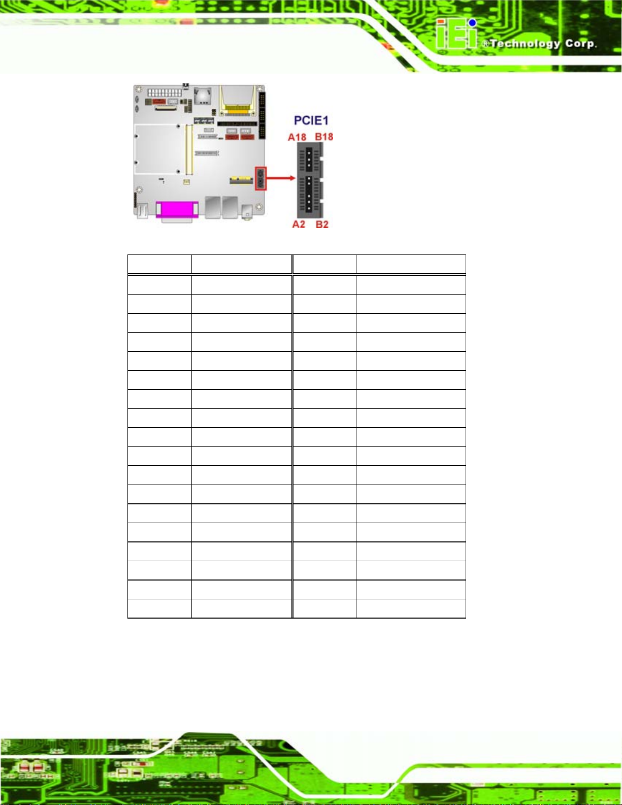
IQ7 Design Guide
Figure 4-12: PCIe x1 Connector Location
Pin Description Pin Description
A1 +12v B1 PRSNT#1
A2 +12v B2 +12v
A3 RSVD B3 +12v
A4 GND B4 GND
A5 SMCLK B5 JTAG2
A6 SMDAT B6 JTAG3
A7 GND B7 JTAG4
A8 +3.3v B8 JTAG5
A9 JTAG1 B9 +3.3v
A10 3.3 Vaux B10 +3.3v
A11 WAKE# B11 PWRGD
A12 RSVD B12 GND
A13 GND B13 REFCLK+
A14 HSOp(0) B14 REFCLKA15 HSOn(0) B15 GND
A16 GND B16 HSIp(0)
A17 PRSNT#2 B17 HSIn(0)
A18 GND B18 GND
Table 4-12: PCIe x1 Slot Pinouts
4.2.12 PCIe Mini Card Slot
CN Label: CN2
Page 41
Page 54

IQ7 Design Guide
CN Type:
CN Location:
CN Pinouts:
PCIe Mini card slot 52-pin, 90°, P=0.8 mm & 180°, 9.0H
5Figure 4-13
See
Table 4-13
See
The PCIe Mini card slot is for installing PCIe Mini expansion cards.
Figure 4-13: PCIe Mini Card Slot Location
Pin Description Pin Description
1 PCIE_WAKE# 2 VCC3
3 N/C 4 GND
5 N/C 6 1.5 V
7 CLKREQ# 8 LFRAME#
9 GND 10 LAD3
11 CLK- 12 LAD2
13 CLK+ 14 LAD1
15 GND 16 LAD0
17 PCIRST# 18 GND
19 LPC 20 VCC3
21 GND 22 PCIRST#
23 PERN2 24 3 VDual
25 PERP2 26 GND
27 GND 28 1.5 V
29 GND 30 SMBCLK
31 PETN2 32 SMBDATA
Page 42
33 PETP2 34 GND
Page 55

IQ7 Design Guide
Pin Description Pin Description
35 GND 36 USBD37 N/C 38 USBD+
39 N/C 40 GND
41 N/C 42 N/C
43 N/C 44 RF_LINK#
45 N/C 46 BLUELED#
47 N/C 48 1.5 V
49 N/C 50 GND
51 N/C 52 VCC3
Table 4-13: PCIe Mini Card Slot Pinouts
4.2.13 Power Button
CN Label: SW2
CN Type:
CN Location:
Button
Figure 4-14
See
The power button turns the power on and off.
Figure 4-14: Power Button Location
4.2.14 QSeven Connector
CN Label: J1
Page 43
Page 56

IQ7 Design Guide
CN Type:
CN Location:
CN Pinouts:
QSeven connector, MXM, 230-pin, 90°, P=0.5 mm
Figure 4-15
See
Table 4-14
See
The QSeven CPU module is installed in this slot.
Figure 4-15: QSeven Connector Location
Pin Description Pin Description
1 GND 2 GND
3 GBE_MDI3- 4 GBE_MDI25 GBE_MDI3+ 6 GBE_MDI2+
7 GBE_LINK100# 8 GBE_LINK1000#
9 GBE_MDI1- 10 GBE_MDI011 GBE_MDI1+ 12 GBE_MDI0+
13 GBE_LINK# 14 GBE_ACT#
15 GBE_CTREF 16 SUS_S5#
17 WAKE# 18 SUS_S3#
19 SUS_STAT# 20 PWRBTN#
21 SLP_BTN# 22 LID_BTN#
23 GND 24 GND
KEY KEY KEY KEY
25 GND 26 PWGIN
Page 44
27 BATLOW# 28 RSTBTN#
Page 57

IQ7 Design Guide
29 SATA0_TX+ 30 SATA1_TX+
31 SATA0_TX- 32 SATA1_TX33 SATA_ACT# 34 GND
35 SATA0_RX+ 36 SATA1_RX+
37 SATA0_RX- 38 SATA1_RX39 GND 40 GND
41 BIOS_DISABLE# 42 SDIO_CLK#
43 SDIO_CD# 44 SDIO_LED
45 SDIO_CMD 46 SDIO_WP
47 SDIO_PWR# 48 SDIO_DAT1
49 SDIO_DAT0 50 SDIO_DAT3
51 SDIO_DAT2 52 SDIO_DAT5
53 SDIO_DAT4 54 SDIO_DAT7
55 SDIO_DAT6 56 RSVD
57 GND 58 GND
59 HDA_SYNC 60 SMB_CLK
61 HDA_RST# 62 SMB_DAT
63 HDA_BITCLK 64 SMB_ALERT#
65 HDA_SDI 66 I2C_CLK
67 HDA_SDO 68 I2C_DAT
69 THRM# 70 WDTRIG#
71 THRMTRIP# 72 WDOUT
73 GND 74 GND
75 USB_P7- 76 USB_P677 USB_P7+ 78 USB_P6+
79 USB_6_7_OC# 80 USB_4_5_OC#
81 USB_P5- 82 USB_P483 USB_P5+ 84 USB_P4+
85 USB_2_3_OC# 86 USB_0_1_OC#
87 USB_P3- 88 USB_P289 USB_P3+ 90 USB_P2+
91 USB_HOST_PRES# 92 USB_HC_SEL
93 USB_P1- 94 USB_P095 USB_P1+ 96 USB_P0+
Page 45
Page 58

97 GND 98 GND
99 LVDS_A0+ 100 LVDS_B0+
101 LVDS_A0- 102 LVDS_B0103 LVDS_A1+ 104 LVDS_B1+
105 LVDS_A1- 106 LVDS_B1107 LVDS_A2+ 108 LVDS_B2+
109 LVDS_A2- 110 LVDS_B2111 LVDS_PPEN 112 LVDS_BLEN
113 LVDS_A3+ 114 LVDS_B3+
115 LVDS_A3- 116 LVDS_B3117 GND 118 GND
119 LVDS_A_CLK+ 120 LVDS_B_CLK+
121 LVDS_A_CLK- 122 LVDS_B_CLK123 LVDS_BLT_CTRL 124 RSVD
IQ7 Design Guide
125 LVDS_DID_DAT 126 LVDS_BLC_DAT
127 LVDS_DID_CLK 128 LVDS_BLC_CLK
129 RSVD 130 RSVD
131 SDVO_BCLK+ 132 SDVO_INT+
133 SDVO_BCLK- 134 SDVO_INT135 GND 136 GND
137 SDVO_GREEN+ 138 SDVO_FLDSTALL+
139 SDVO_GREEN- 140 SDVO_FLDSTALL141 GND 142 GND
143 SDVO_BLUE+ 144 SDVO_TVCLKIN+
145 SDVO_BLUE- 146 SDVO_TVCLKIN147 GND 148 GND
149 SDVO_RED+ 150 SDVO_CTRL_DAT
151 SDVO_RED- 152 SDVO_CTRL_CLK
153 HDMI_HPD# 154 DP_HPD#
155 PCIE_CLK_REF+ 156 PCIE_WAKE#
Page 46
157 PCIE_CLK_REF- 158 PCIE_RST#
159 GND 160 GND
161 PCIE3_TX+ 162 PCIE3_RX+
163 PCIE3_TX- 164 PCIE3_RX-
Page 59

IQ7 Design Guide
165 GND 166 GND
167 PCIE2_TX+ 168 PCIE2_RX+
169 PCIE2_TX- 170 PCIE2_RX171 EXCD0_PERST# 172 EXCD1_PERST#
173 PCIE1_TX+ 174 PCIE1_RX+
175 PCIE1_TX- 176 PCIE1_RX177 EXCD0_CPPE# 178 EXCD1_CPPE#
179 PCIE0_TX+ 180 PCIE0_RX+
181 PCIE0_TX- 182 PCIE0_RX183 GND 184 GND
185 LPC_AD0 186 LPC_AD1
187 LPC_AD2 188 LPC_AD3
189 LPC_CLK 190 LPC_FRAME#
191 SERIRQ 192 LPC_LDRQ#
193 VCC_RTC 194 SPKR
195 FAN_TACHOIN 196 FAN_PWMOUT
197 GND 198 GND
199 RSVD 200 RSVD
201 RSVD 202 RSVD
203 RSVD 204 MFG_NC4
205 VCC_5V_SB 206 VCC_5V_SB
207 MFG_NC0 208 MFG_NC2
209 MFG_NC1 210 MFG_NC3
211 VCC 212 VCC
213 VCC 214 VCC
215 VCC 216 VCC
217 VCC 218 VCC
219 VCC 220 VCC
221 VCC 222 VCC
223 VCC 224 VCC
225 VCC 226 VCC
227 VCC 228 VCC
Page 47
Page 60

229 VCC 230 VCC
Table 4-14: QSeven Connector Pinouts
4.2.15 Reset Button
CN Label: SW1
IQ7 Design Guide
CN Type:
CN Location:
Press the reset button to reset the system.
Figure 4-16: Reset Button Location
Button
Figure 4-16
See
4.2.16 SATA Drive Connectors
Page 48
CN Label: S_ATA1, S_ATA2, S_ATA3
CN Type:
CN Location:
The SATA connectors can be connected to SATA peripheral devices like hard drives and
optical drives.
SATA drive connectors
5Figure 4-17
See
Page 61

IQ7 Design Guide
Figure 4-17: SATA Drive Connector Locations
4.2.17 SATA Power Connectors
CN Label: CN17, CN21, CN23
CN Type:
CN Location:
CN Pinouts:
The SATA power connectors provide power to connected SATA devices like SATA hard
drives or optical drives.
4-pin wafer (1x4), 180°, P=2.5 mm
Figure 4-18
See
Table 4-15
See
Figure 4-18: SATA Power Connector Locations
Page 49
Page 62

Pin Description
1 +5 V
2 GND
3 GND
4 +12 V
Table 4-15: SATA Power Connector Pinouts
4.2.18 SDVO Connector
CN Label: SDVO1
IQ7 Design Guide
CN Type:
CN Pinouts:
Flat cable
Table 4-8
See
The SDVO connector is an optional extra that can attach to an SDVO graphics card.
Pin Description Pin Description
1 RESET# 2 GROUND
3 DATA 7 4 DATA 8
5 DATA 6 6 DATA 9
7 DATA 5 8 DATA 10
9 DATA 4 10 DATA 11
11 DATA 3 12 DATA 12
13 DATA 2 14 DATA 13
15 DATA 1 16 DATA 14
17 DATA 0 18 DATA 15
19 GROUND 20 N/C
Page 50
21 IDE DRQ 22 GROUND
23 IOW# 24 GROUND
25 IOR# 26 GROUND
27 IDE CHRDY 28 GROUND
29 IDE DACK 30 GROUND–DEFAULT
31 INTERRUPT 32 N/C
33 SA1 34 N/C
Page 63

IQ7 Design Guide
Pin Description Pin Description
35 SA0 36 SA2
37 HDC CS0# 38 HDC CS1#
39 HDD ACTIVE# 40 GROUND
41 VCC 42 VCC
43 GROUND 44 N/C
Table 4-16: IDE Connector Pinouts
4.2.19 Serial Port Connectors
CN Label: COM2, COM3, COM4
CN Type:
CN Location:
CN Pinouts:
10-pin box header (2x5), 180°, P=2.5 mm
Figure 4-19
See
Table 4-17
See
The serial ports provide RS-232 transmission capabilities.
Figure 4-19: Serial Port Connector Locations
Pin Description Pin Description
1 DCD1 2 DSR1
3 RXD1 4 RTS1
Page 51
Page 64

Pin Description Pin Description
5 TXD1 6 CTS1
7 DTR1 8 RI1
9 GND1 10 GND1
Table 4-17: Serial Port Connector Pinouts
4.2.20 TTL Connector
CN Label: CN16
IQ7 Design Guide
CN Type:
CN Location:
CN Pinouts:
40-pin crimp (2x20) DF-13, 180°, P=1.25 mm
Figure 4-20
See
Table 4-18
See
The TTL connector is for an LCD panel connected to the board.
Page 52
Figure 4-20: TTL Connector Location
Pin Description Pin Description
1 +3.3V 2 +3.3V
3 GND 4 GND
5 +3.3V 6 +3.3V
7 SMB_DAT 8 GND
9 TFT_B0 10 TFT_B1
Page 65

IQ7 Design Guide
Pin Description Pin Description
11 TFT_B2 12 TFT_B3
13 TFT_B4 14 TFT_B5
15 TFT_B6 16 TFT_B7
17 TFT_G0 18 TFT_G1
19 TFT_G2 20 TFT_G3
21 TFT_G4 22 TFT_G5
23 TFT_G6 24 TFT_G7
25 TFT_R0 26 TFT_R1
27 TFT_R2 28 TFT_R3
29 TFT_R4 30 TFT_R5
31 TFT_R6 32 TFT_R7
33 GND 34 GND
35 VOCLK 36 VSYNC
37 VDEN 38 HSYNC
39 SMB_CLK 40 LVDS_BKLT_EN
Table 4-18: TTL Connector Pinouts
4.2.21 USB Connector
CN Label: USB5
CN Type:
CN Location:
CN Pinouts:
The USB header can connect to two USB devices.
8-pin header (2x4) 180°, P=2.0 mm
5Figure 4-21
See
5Table 4-19
See
Page 53
Page 66

IQ7 Design Guide
Figure 4-21: USB Connector Locations
Pin Description Pin Description
1 VCC 2 GND
3 DATA- 4 DATA+
5 DATA+ 6 DATA7 GND 8 VCC
Table 4-19: USB Port Connector Pinouts
Page 54
Page 67

IQ7 Design Guide
4.3 External Interface Connectors
5Figure 4-22 shows the IQ7-DB-MITX motherboard external interface connectors. The
IQ7-DB-MITX on-board external interface connectors are shown in
Figure 4-22: External Interface Connectors
4.3.1 Audio Connector
Figure 4-22.
CN Label: AUDIO1
CN Type:
CN Location:
CN Pinouts:
The audio jacks connect to external audio devices.
Line Out port (Lime): Connects to a head phone or a speaker.
Microphone (Pink): Connects a microphone.
Audio jacks, 14-pin, 90°, P=2.5 mm
Figure 4-22
See
Table 4-20
See
Page 55
Page 68

IQ7 Design Guide
Figure 4-23: Audio Connector
Pin Description Pin Description
1 Ground 2 LMIC1-L
3 NC 4 NC
5 LMIC1-R 22 LFRONT-L
23 NC 24 NC
25 LFRONT-R
Table 4-20: Audio Connector Pinouts
4.3.2 Ethernet Connector
CN Label: LAN1_USB01, LAN2_USB23
CN Type:
CN Location:
CN Pinouts:
A 10/100/1000 Mb/s connection can be made to a Local Area Network.
Pin Description Pin Description
1 MDIA3- 5 MDIA1+
2 MDIA3+ 6 MDIA2+
3 MDIA2- 7 MDIA04 MDIA1- 8 MDIA0+
RJ-45
5Figure 4-22
See
5Table 4-21
See
Page 56
Table 4-21: Ethernet Connector Pinouts
Page 69

IQ7 Design Guide
Figure 4-24: Ethernet Connector
The RJ-45 Ethernet connector has two status LEDs, one green and one yello w. The green
LED indicates activity on the port and the yellow LED indicates the port is linked.
SPEED LED LINK LED
Status Description Status Description
GREEN ON: 100 MB
OFF: 10 MB
YELLOW ON: Linked
Flashing: Activity
Table 4-22: Connector LEDs
4.3.3 Keyboard and Mouse Connector
CN Label: KB_MS1
CN Type:
CN Location:
CN Pinouts:
The IQ7-DB-MITX has two PS/2 connectors on the mounting bracket for easy connection
to a PS/2 keyboard and PS/2 mouse.
PS/2
5Figure 4-22
See
5Table 4-23 and 5Figure 4-25
See
Page 57
Page 70

IQ7 Design Guide
Figure 4-25: PS/2 Connector
Pin Description Pin Description
1 KEYBOARD DATA 7 MOUSE DATA
2 NC 8 NC
3 GND 9 GND
4 +5 V 10 +5 V
5 KEYBOARD CLOCK 11 MOUSE DATA
6 NC 12 NC
Table 4-23: PS/2 Connectors
4.3.4 Parallel Port Connector
CN Label: LPT1
CN Type:
CN Location:
CN Pinouts:
The parallel port connects to parallel port device, typically a printer.
D-SUB 25-pin 90° H=31.6 mm
Figure 4-22
See
Table 4-24
See
Page 58
Pin Description Pin Description
1 STROBE# 14 AUTO FORM FEED #
2 DATA 0 15 ERROR#
Page 71

IQ7 Design Guide
Pin Description Pin Description
3 DATA 1 16 INITIALIZE
4 DATA 2 17 PRINTER SELECT LN#
5 DATA 3 18 GROUND
6 DATA 4 19 GROUND
7 DATA 5 20 GROUND
8 DATA 6 21 GROUND
9 DATA 7 22 GROUND
10 ACKNOWLEDGE 23 GROUND
11 BUSY 24 GROUND
12 PAPER EMPTY 25 GROUND
13 PRINTER SELECT
Table 4-24: Parallel Port Connector Pinouts
Figure 4-26: Parallel Port Connector Location
4.3.5 Serial Port Connector
CN Label: COM1
CN Type:
CN Location:
CN Pinouts:
The RS-232 serial connector provides serial connection in the RS-232 mode.
DB-9 connector
See
See
Figure 4-22
5Table 4-25 and 5Figure 4-27
Pin Description
1 DCD
2 RXD
3 TXD
Page 59
Page 72

Pin Description
4 DTR
5 GND
6 DSR
7 RTS
8 CTS
9 RI
10 GND
11 GND
IQ7 Design Guide
Table 4-25: Serial Port Pinouts
Figure 4-27: Serial Port Pinout Locations
4.3.6 USB Ports
CN Label: LAN1_USB01, LAN2_USB23, USB4_7
CN Type:
CN Location:
CN Pinouts:
The USB ports attach to standard USB devices.
Pin Description
1 VCC
2 Data3 Data+
USB Combo ports
Figure 4-22
See
5Table 4-26
See
Page 60
Page 73
IQ7 Design Guide
Pin Description
4 Ground
Table 4-26: USB Connector Pinouts
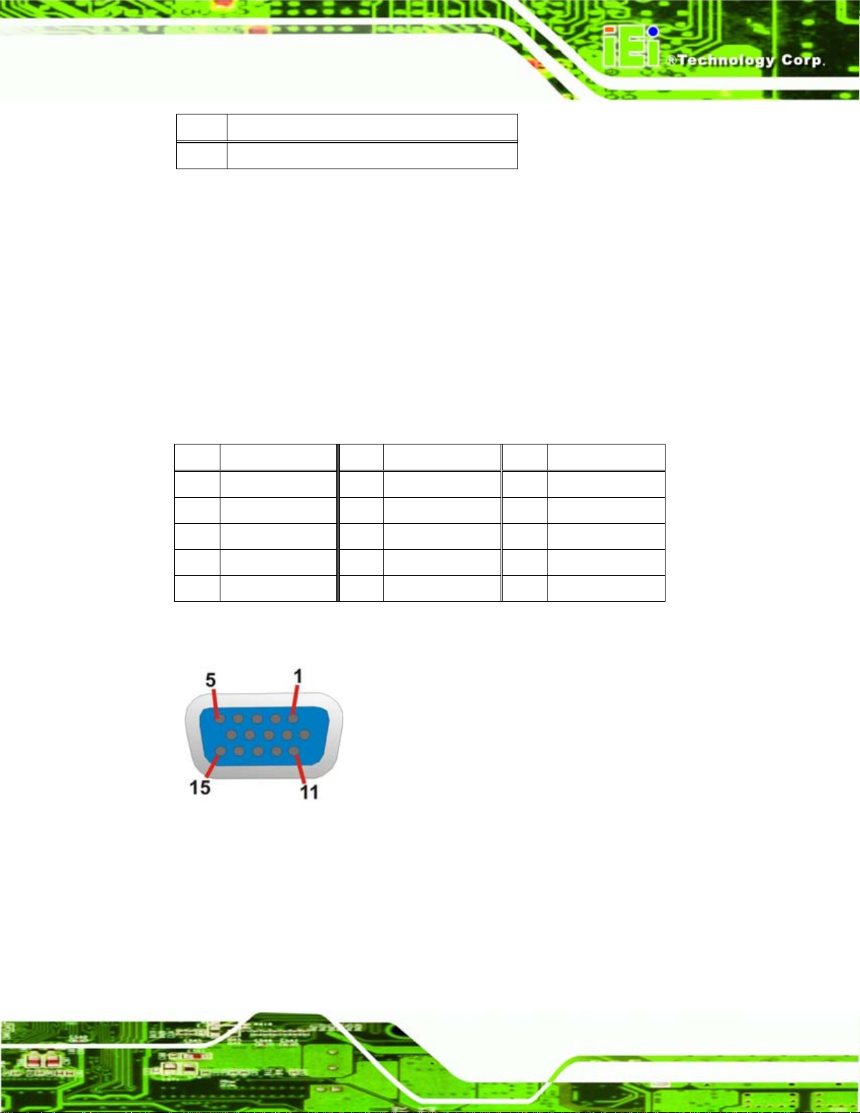
4.3.7 VGA Connector
CN Label: CON1
CN Type:
CN Location:
CN Pinouts:
D-sub 15-pin female connector
5Figure 4-22
See
5Figure 4-28 and 5Table 4-27
See
The standard 15-pin female VGA connector connects to a CRT or LCD monitor.
Pin Description Pin Description Pin Description
1 RED 6 GROUND 11 NC
2 GREEN 7 GROUND 12 SDA
3 BLUE 8 GROUND 13 HSYNC
4 +5V 9 NC 14 VSYNC
5 GROUND 10 GROUND 15 SCL
Table 4-27: VGA Connector Pinouts
Figure 4-28: VGA Connector
Page 61
Page 74

4.4 Jumper Settings
NOTE:
A jumper is a metal bridge that is used
to close an electrical circuit. It consists
of two metal pins and a small metal clip
(often protected by a plastic cover) that
slides over the pins to connect them.
To CLOSE/SHORT a jumper means
connecting the pins of the jumper with
the plastic clip and to OPEN a jumper means removing the plastic clip
from a jumper.
IQ7 Design Guide
Before the IQ7 Design Guide is installed in the system, the jumpers must be set in
accordance with the desired configuration. The jumpers on the IQ7 Design Guide are
listed in
Description Label Type
AT/ATX mode selection JP8 & SW5 6-pin header & switch
Clear CMOS JP6 3-pin header
CompactFlash® Master/Slave JP4 3-pin header
CompactFlash® voltage JP3 3-pin header
LAN & PCIe enable/disable SW3 Switch
TTL voltage selection J_VLVDS1 3-pin header
SATA & graphics settings SW4 Switch
TTL enable/disable SW5 Switch
Table 4-28: Jumpers
5Table 4-28.
Page 62
Page 75

IQ7 Design Guide
Figure 4–29: Jumpers
4.4.1 AT/ATX Mode Selection
Jumper Label: JP8 & SW5
Jumper Type:
Jumper Settings:
Jumper Location:
Set both of the jumpers select AT or ATX power mode for the IQ7 Design Guide. AT
power mode limits the system to on/off. ATX allows the system to use various power
saving states and enter a standby state, so the system can be turned on remotely over a
network. The settings on both jumpers should be the same.
JP8 Description
1-2 ATX mode
3-4 AT mode
5-6 No function
6-pin header & switch
5Table 4-29 & Table 4-30
See
Figure 4–29
See
Table 4-29: AT/ATX Mode Selection
Page 63
Page 76

SW5 Description
1-On AT mode
1-Off ATX mode
Table 4-30: AT/ATX Mode Selection
4.4.2 Clear CMOS Jumper
Jumper Label: JP8
IQ7 Design Guide
Jumper Type:
Jumper Settings:
Jumper Location:
3-pin header
Table 4-31
See
Figure 4–29
See
If the IQ7 Design Guide fails to boot due to improper BIOS settings, the clear CMOS
jumper clears the CMOS data and resets the system BIOS information. To do this, use the
jumper cap to close pins 2 and 3 for a few seconds then reinstall the jumper clip back to
pins 1 and 2.
If the “CMOS Settings Wrong” message is displayed during the boot up process, the fault
may be corrected by pressing the F1 to enter the CMOS Setup menu. Do one of the
following:
Enter the correct CMOS setting
Load Optimal Defaults
Load Failsafe Defaults.
Page 64
After having done one of the above, save the changes and exit the CMOS Setup menu.
The clear CMOS jumper settings are shown in
Pin Description
1-2 Keep CMOS Setup
2-3 Clear CMOS Setup
5Table 4-31.
Table 4-31: Clear CMOS Jumper Settings
Page 77

IQ7 Design Guide
4.4.3 CompactFlash® Master/Slave Selection
Jumper Label: JP4
Jumper Type:
Jumper Settings:
Jumper Location:
Sets the CompactFlash® slot as the IDE primary master or primary slave.
Pin Description
1-2 Slave
2-3 Master
Table 4-32: CompactFlash® Master/Slave Selection
3-pin header
Table 4-32
See
Figure 4–29
See
4.4.4 CompactFlash® Voltage Selection
Jumper Label: JP3
Jumper Type:
Jumper Settings:
3-pin header
Table 4-33
See
Figure 4–29
Jumper Location:
Sets the voltage of the power supplied to the CompactFlash® card.
Pin Description
1-2 5.0 V
2-3 3.3 V
Table 4-33: CompactFlash® Voltage Selection
See
4.4.5 LAN & PCIe Enable/Disable
Jumper Label: SW3
Jumper Type:
Jumper Settings:
Jumper Location:
4 switches
Table 4-34
See
Figure 4–29
See
Page 65
Page 78

These settings enable and disabled these devices on the IQ7 Design Guide.
SW3 Description
1-On & 2-Off PCIe x1 slot enabled & LAN2 disabled
1-Off & 2-On LAN2 enabled & PCIe x1 slot disabled
3-On & 4-Off LAN1 enabled & PCIe Mini card disabled
3-Off & 4-On PCIe Mini enabled & LAN1 disabled
Table 4-34: LAN & PCIe Enable/Disable
4.4.6 TTL Voltage Selection
Jumper Label: J_VLVDS1
IQ7 Design Guide
Jumper Type:
Jumper Settings:
Jumper Location:
3-pin header
Table 4-35
See
Figure 4–29
See
Selects the voltage of the LVDS connector.
Pin Description
1-2 3.3 V
2-3 5.0 V
Table 4-35: LVDS Voltage Selection
4.4.7 SATA & Graphics Settings
Jumper Label: SW4
Jumper Type:
Jumper Settings:
4 switches
Table 4-36
See
Page 66
Figure 4–29
Jumper Location:
See
These settings enable and disabled these devices on the IQ7 Design Guide.
SW4 Description
1–On & 2-Off SDVO enabled & VGA disabled
1-Off & 2-On VGA enabled & SDVO disabled
Page 79

IQ7 Design Guide
SW4 Description
3-On SATA as master
3-Off SATA as slave
4-On SATA disable
4-Off SATA enabled
Table 4-36: LAN & PCIe Enable/Disable
4.4.8 TTL Enabled/Disable
Jumper Label: SW5
Jumper Type:
Jumper Settings:
Jumper Location:
Switch
Table 4-37
See
Figure 4–29
See
Disables/enables the TTL connection.
Pin Description
2-On TTL disable
2-Off TTL enable
Table 4-37: TTL Enable/Disable
Page 67
Page 80
IQ7 Design Guide
Chapter
5
5 Installation
Page 68
Page 81

IQ7 Design Guide
5.1 Anti-static Precautions
WARNING:
Failure to take ESD precautions during installation may result in
permanent damage to the device and severe injury to the user.
Electrostatic discharge (ESD) can cause serious damage to electronic components. Dry
climates are especially susceptible to ESD. It is therefore critical to strictly adhere to the
following anti-static precautions when any electrical component is handled.
Wear an anti-static wristband: - Wearing a simple anti-static wristband can
help to prevent ESD from damaging the board.
Self-grounding:- Before handling the board touch any grounded conducting
material. During the time the board is handled, frequently touch any
conducting materials that are connected to the ground.
Use an anti-static pad: When configuring, place on an antic-static pa d. This
reduces the possibility of ESD damage.
Only handle the edges of the PCB:-: When handling the PCB, hold the PCB
by the edges.
5.2 Installation Considerations
NOTE:
The following installation notices and installation considerations should
be read and understood before installation. All installation notices
should be strictly adhered to. Failing to adhere to these precautions
may lead to severe damage of the product and injury to the person
installing the motherboard.
Page 69
Page 82

IQ7 Design Guide
WARNING:
The installation instructions described in this manual should be
carefully followed in order to prevent damage to the product, its
components and injury to the user.
Before and during the installation please DO the following:
Read the user manual:
o The user manual provides a complete description of the installation
instructions and configuration options.
Wear an electrostatic discharge cuff (ESD):
o Electronic components are easily damaged by ESD. Wearing an ESD cuff
removes ESD from the body and helps prevent ESD damage.
Place the product on an antistatic pad:
o When installing or configuring the motherboard, place it on an antistatic
pad. This helps to prevent potential ESD damage.
Turn all power to the product off:
o When working with the product, make sure that it is disconnected from all
power supplies and that no electricity is being fed into the system.
Before and during installation, DO NOT:
DO NOT remove any of the stickers on the PCB board. These stickers are
required for warranty validation.
DO NOT use the product before verifying all the cables and power connectors
are properly connected.
DO NOT allow screws to come in contact with the PCB circuit, co nnector pins,
or its components.
Page 70
Page 83

IQ7 Design Guide
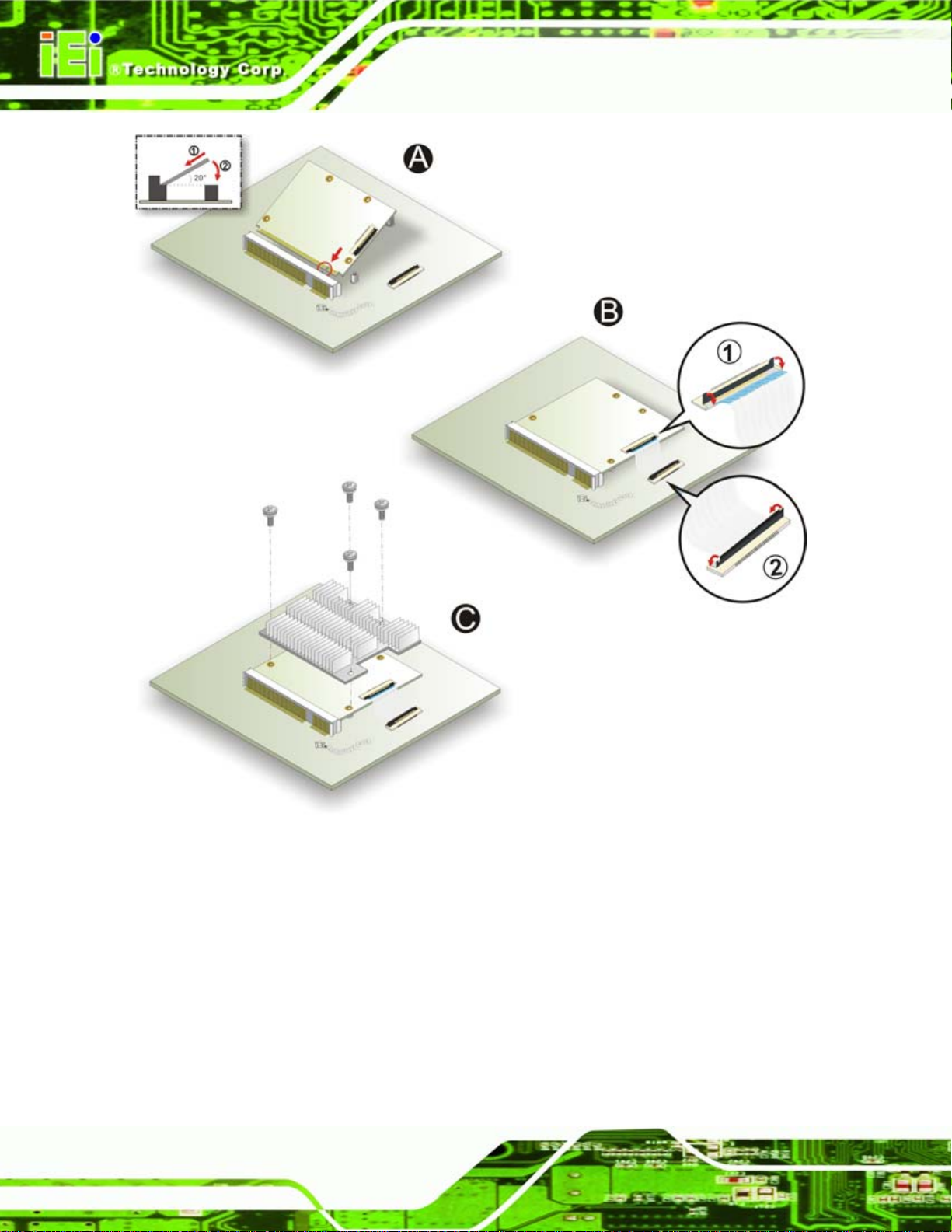
5.3 CPU Module Installation
WARNING:
Only install the QSeven CPU module on a compatible QSeven
baseboard like the IQ7-DB-MITX. Attempting to force another CPU
card to fit can cause permanent damage to the system.
To install the CPU module, refer to 6Figure 5-1.
Page 71
Page 84
IQ7 Design Guide
Page 72
Figure 5-1: Installing the QSeven CPU Module
Step 1: Insert the CPU module into the QSeven slot.
Step 2: Press down with the heatsink on top.
Step 3: Tighten the screws to hold down the CPU card and the heatsink.Step 0:
Page 85

IQ7 Design Guide
Chapter
6
6 BIOS
Page 73
Page 86

6.1 Introduction
The BIOS is programmed onto the BIOS chip. The BIOS setup program allows changes to
certain system settings. This chapter outlines the options that can be changed.
6.1.1 Starting Setup
The AMI BIOS is activated when the computer is turned on. The setup program can be
activated in one of two ways.
IQ7 Design Guide
1. Press the D
2. Press the D
appears on the screen. 0.
If the message disappears before the D
again.
ELETE key as soon as the system is turned on or
ELETE key when the “Press Del to enter SETUP” message
ELETE key is pressed, restart the computer and try
6.1.2 Using Setup
Use the arrow keys to highlight items, press ENTER to select, use the PageUp and
PageDown keys to change entries, press F1 for help and press E
keys are shown in.
Key Function
Up arrow Move to previous item
Down arrow Move to next item
Left arrow Move to the item on the left hand si de
SC to quit. Navigation
Page 74
Right arrow Move to the item on the right hand side
Esc key Main Menu – Quit and not save changes into CMOS
Status Page Setup Menu and Option Page Setup Menu --
Exit current page and return to Main Menu
Page Up key Increase the numeric value or make changes
Page Dn key Decrease the numeric value or make changes
F1 key General help, only for Status Page Setup Menu and Option
Page Setup Menu
Page 87

IQ7 Design Guide
Key Function
F2 /F3 key Change color from total 16 colors. F2 to select color
F10 key Save all the CMOS changes, only for Main Menu
Table 6-1: BIOS Navigation Keys
6.1.3 Getting Help
When F1 is pressed a small help window describing the appropriate keys to use and the
forward.
possible selections for the highlighted item appears. To exit the Help Window press E
the F1 key again.
6.1.4 Unable to Reboot After Configuration Changes
If the computer cannot boot after changes to the system configuration is made, CMOS
defaults. Use the jumper described in Chapter 5.
6.1.5 BIOS Menu Bar
The menu bar on top of the BIOS screen has the following main items:
Main – Changes the basic system configuration.
Advanced – Changes the advanced system settings.
PCIPnP – Changes the advanced PCI/PnP Settings
Boot – Changes the system boot configuration.
Security – Sets User and Supervisor Passwords.
Chipset – Changes the chipset settings.
SC or
Power – Changes power management settings.
Exit – Selects exit options and loads default settings
The following sections completely describe the configuration options found in the menu
items at the top of the BIOS screen and listed above.
Page 75
Page 88

IQ7 Design Guide
6.2 Main
The Main BIOS menu (BIOS Menu 1) appears when the BIOS Setup program is entered.
The Main menu gives an overview of the basic system information.
BIOS SETUP UTILITY
Main Advanced PCIPNP Boot Security Chipset Exit
System Overview
⎯⎯⎯⎯⎯⎯⎯⎯⎯⎯⎯⎯⎯⎯⎯⎯⎯⎯⎯⎯⎯⎯⎯⎯⎯⎯⎯⎯⎯⎯⎯
AMIBIOS
Version :08.00.15
Build Date :12/18/08
ID: :B137MR10
Processor
Intel® Atom CPU Z510 @ 1.10 GHz
Speed :1100MHz
Count :1
System Memory
Size :1019MB
System Time [14:20:27]
System Time [Tue 05/06/2008]
CMC Lo-Module: 0D2.023x, Hi-Module:0D2.016x
v02.61 ©Copyright 1985-2006, American Megatrends, Inc.
Use [ENTER], [TAB] or
[SHIFT-TAB] to select a
field.
Use [+] or [-] to
configure system time.
ÅÆ
Select Screen
↑ ↓ Select Item
Enter Go to SubScreen
F1 General Help
F10 Save and Exit
ESC Exit
BIOS Menu 1: Main
System Overview
The System Overvie w lists a brief summary of different system components. Th e fields in
System Overview cannot be changed. The items shown in the system overview include:
AMI BIOS: Displays auto-detected BIOS information
Processor: Displays auto-detected CPU specifications
System Memory: Displays the auto-detected system memory.
Page 76
o Version: Current BIOS version
o Build Date: Date the current BIOS version was made
o ID: Installed BIOS ID
o Type: Names the currently installed processor
o Speed: Lists the processor speed
o Count: The number of CPUs on the motherboard
Page 89

IQ7 Design Guide
o Size: Lists memory size
The System Overview field also has two user configurable fields:
System Time [xx:xx:xx]
Use the System Time option to set the system time. Manually enter the hours, minutes
and seconds.
System Date [xx/xx/xx]
Use the System Date option to set the system date. Manually enter the day, month and
year.
6.3 Advanced
Use the Advanced menu (BIOS Menu 2) to configure the CPU and peripheral devices
through the following sub-menus:
BIOS SETUP UTILITY
Main Advanced PCIPNP Boot Security Chipset Exit
Advanced Settings
⎯⎯⎯⎯⎯⎯⎯⎯⎯⎯⎯⎯⎯⎯⎯⎯⎯⎯⎯⎯⎯⎯⎯⎯⎯⎯⎯⎯⎯⎯⎯
WARNING: Setting wrong values in below sections may cause
system to malfunction
> CPU Configuration
> IDE Configuration
> SuperIO Configuration
> Hardware Health Configuration
> Remote Access Configuration
> USB Configuration
v02.61 ©Copyright 1985-2006, American Megatrends, Inc.
BIOS Menu 2: Advanced
Configure CPU
ÅÆ
Select Screen
↑ ↓ Select Item
Enter Go to SubScreen
F1 General Help
F10 Save and Exit
ESC Exit
Page 77
Page 90

IQ7 Design Guide
6.3.1 CPU Configuration
Use the CPU Configuration menu (BIOS Menu 3) to view detailed CPU specifications
and configure the CPU.
BIOS SETUP UTILITY
Main Advanced PCIPNP Boot Security Chipset Exit
Configure Advanced CPU Settings
Module Version:3F.14
⎯⎯⎯⎯⎯⎯⎯⎯⎯⎯⎯⎯⎯⎯⎯⎯⎯⎯⎯⎯⎯⎯⎯⎯⎯⎯⎯⎯⎯⎯⎯
Manufacturer :Intel®
Intel® Atom CPU Z510 @ 1.10 GHz
Frequency :1.10GHz
FSB Speed :400Hz
Cache L1 :24 KB
Cache L2 :512 KB
Ratio Actual Value:11
ÅÆ
Select Screen
↑ ↓ Select Item
Enter Go to SubScreen
F1 General Help
F10 Save and Exit
ESC Exit
v02.61 ©Copyright 1985-2006, American Megatrends, Inc.
BIOS Menu 3: CPU Configuration
The CPU Configuration menu (BIOS Menu 3) lists the following CPU details:
Manufacturer: Lists the name of the CPU manufacturer
Brand String: Lists the brand name of the CPU being used
Frequency: Lists the CPU processing speed
FSB Speed: Lists the FSB speed
Cache L1: Lists the CPU L1 cache size
Cache L2: Lists the CPU L2 cache size
Ratio actual value is the ratio of the frequency to the clock speed
Page 78
Page 91

IQ7 Design Guide
6.3.2 IDE Configuration
Use the IDE Configuration menu (BIOS Menu 4) to change and/or set the configuration
of the IDE devices installed in the system.
BIOS SETUP UTILITY
Main Advanced PCIPNP Boot Security Chipset Exit
IDE Configuration
⎯⎯⎯⎯⎯⎯⎯⎯⎯⎯⎯⎯⎯⎯⎯⎯⎯⎯⎯⎯⎯⎯⎯⎯⎯⎯⎯⎯⎯⎯⎯
Onboard PCI IDE Controller [Primary]
> Primary IDE Master : [Not Detected]
> Primary IDE Slave : [Not Detected]
Options
Primary
Disabled
ÅÆ
Select Screen
↑ ↓ Select Item
Enter Go to SubScreen
F1 General Help
F10 Save and Exit
ESC Exit
v02.61 ©Copyright 1985-2006, American Megatrends, Inc.
BIOS Menu 4: IDE Configuration
Onboard PCI IDE Controller [Primary]
Use the Onboard PCI IDE Controller to configure the IDE channel.
Î
Primary DEFAULT
Î
Disabled
IDE Master and IDE Slave
When entering setup, BIOS auto detects the presence of IDE devices. BIOS displays the
status of the auto detected IDE devices. The following IDE devices are detected and are
shown in the IDE Configuration menu:
Primary IDE Master
Primary IDE Slave
IDE drives are enabled
IDE drives disabled
Page 79
Page 92

S
IQ7 Design Guide
6.3.2.1 IDE Master, IDE Slave
Use the IDE Master and IDE Slave configuration menu to view both primary and
secondary IDE device details and configure the IDE devices connected to the system.
BIOS SETUP UTILITY
Main Advanced PCIPNP Boot Security Chipset Exit
Primary IDE Master
⎯⎯⎯⎯⎯⎯⎯⎯⎯⎯⎯⎯⎯⎯⎯⎯⎯⎯⎯⎯⎯⎯⎯⎯⎯⎯⎯⎯⎯⎯⎯
Device :Not Detected
Type [Auto]
LBA/Large Mode [Auto]
Block (Multi-Sector Transfer) [Auto]
PIO Mode [Auto]
DMA Mode [Auto]
S.M.A.R.T. [Auto]
32Bit Data Transfer [Enabled]
elect the type of device
connected to the system
ÅÆ
Select Screen
↑ ↓ Select Item
Enter Go to SubScreen
F1 General Help
F10 Save and Exit
ESC Exit
v02.61 ©Copyright 1985-2006, American Megatrends, Inc.
BIOS Menu 5: IDE Master and IDE Slave Configuration
Auto-Detected Drive Parameters
The “grayed-out” items in the left frame are IDE disk drive parameters automatically
detected from the firmware of the selected IDE disk drive. The drive parameters are listed
as follows:
Device: Lists the device type (e.g. hard disk, CD-ROM etc.)
Type: Indicates the type of devices a user ca n manually select
Vendor: Lists the device manufacturer
Size: List the storage capacity of the device.
LBA Mode: Indicates whether the LBA (Logical Block Addressing) is a method
of addressing data on a disk drive is supported or not.
Block Mode: Block mode boosts IDE drive performance by increasing the
amount of data transferred. Only 512 bytes of data can be transferred per
interrupt if block mode is not used. Block mode allows transfers of up to 64 KB
per interrupt.
PIO Mode: Indicates the PIO mode of the installed device.
Page 80
Page 93

IQ7 Design Guide
Async DMA: Indicates the highest Asynchronous DMA Mode that is
Ultra DMA: Indicates the highest Synchronous DMA Mode that is supported.
S.M.A.R.T.: Indicates whether or not the Self-Monitoring Analysis and
32Bit Data Transfer: Enables 32-bit data transfer.
Type [Auto]
Use the Type BIOS option select the type of device the AMIBIOS attempts to boot from
after the Power-On Self-Test (POST) is complete.
supported.
Reporting Technology protocol is supported.
Î
Not Installed
Î
Auto DEFAULT
Î
CD/DVD
Î
ARMD
BIOS is prevented from searching for an IDE disk
drive on the specified channel.
The BIOS auto detects the IDE disk drive type
attached to the specified channel. This setting should
be used if an IDE hard disk drive is attached to the
specified channel.
The CD/DVD option specifies that an IDE CD-ROM
drive is attached to the specified IDE channel. The
BIOS does not attempt to search for other types of
IDE disk drives on the specified channel.
This option specifies an ATAPI Removable Media
Device. These include, but are not limited to:
ZIP
LS-120
LBA/Large Mode [Auto]
Use the LBA/Large Mode option to disable or enable BIOS to auto detects LBA (Logical
Block Addressing). LBA is a method of addressing data on a disk drive. In LBA mode, the
maximum drive capacity is 137 GB.
Î
Disabled
BIOS is prevented from using the LBA mode control on
the specified channel.
Page 81
Page 94

IQ7 Design Guide
Î
Auto DEFAULT
Block (Multi Sector Transfer) [Auto]
Use the Block (Multi Sector Transfer) to disable or enable BIOS to auto detect if the
device supports multi-sector transfers.
Î
Disabled
Î
Auto DEFAULT
PIO Mode [Auto]
BIOS auto detects the LBA mode control on the specified
channel.
BIOS is prevented from using Multi-Sector T ran sfer on the
specified channel. The data to and from the device occurs
one sector at a time.
BIOS auto detects Multi-Sector Transfer support on the
drive on the specified channel. If supported the data
transfer to and from the device occurs multiple sectors at
a time.
Use the PIO Mode option to select the IDE PIO (Programmable I/O) mode program timing
cycles between the IDE drive and the programmable IDE controller. As the PIO mode
increases, the cycle time decrease s.
Î
Auto DEFAULT
Î
0
Î
1
Î
2
Î
3
Î
4
BIOS auto detects the PIO mode. Use this value if the IDE disk
drive support cannot be determined.
PIO mode 0 selected with a maximum transfer rate of 3.3 MB/s
PIO mode 1 selected with a maximum transfer rate of 5.2 MB/s
PIO mode 2 selected with a maximum transfer rate of 8.3 MB/s
PIO mode 3 selected with a maximum transfer rate of 11.1 MB/s
PIO mode 4 selected with a maximum transfer rate of 16.6 MB/s
(This setting generally works with all hard disk drives
manufactured after 1999. For other disk drives, such as IDE
CD-ROM drives, check the specifications of the drive.)
Page 82
Page 95

IQ7 Design Guide
DMA Mode [Auto]
Use the DMA Mode BIOS selection to adjust the DMA mode options.
Î
Auto DEFAULT
Î
SWDMA0
Î
SWDMA1
Î
SWDMA2
Î
MWDMA0
Î
MWDMA1
Î
MWDMA2
Î
UDMA0
Î
UDMA1
Î
UDMA2
Î
UDMA3
BIOS auto detects the DMA mode. Use this value if the IDE
disk drive support cannot be determined.
Single Word DMA mode 0, max transfer rate: 2.1 MB/s
Single Word DMA mode 1, max transfer rate: 4.2 MB/s
Single Word DMA mode 2, max transfer rate: 8.3 MB/s
Multi Word DMA mode 0, max transfer rate: 4.2 MB/s
Multi Word DMA mode 1, max transfer rate: 13.3 MB/s
Multi Word DMA mode 2, max transfer rate: 16.6 MB/s
Ultra DMA mode 0, max transfe r rate: 16.6 MB/s
Ultra DMA mode 1, max transfe r rate: 25 MB/s
Ultra DMA mode 2, max transfe r rate: 33.3 MB/s
Ultra DMA mode 3, max transfer rate: 44 MB/s (To use this
mode, it is required that an 80-conductor ATA cable is used.)
Î
UDMA4
Î
UDMA5
S.M.A.R.T [Auto]
Use the S.M.A.R.T option to auto-detect, disable or enable Self-Monitoring Analysis and
Reporting Technology (SMART) on the drive on the specified channel. S.M.A.R.T predicts
impending drive failures. The S.M.A.R.T BIOS option enables or disables this function.
Î
Auto DEFAULT
Î
Disabled
Î
Enabled
Ultra DMA mode 4, max transfer rate: 66.6 MB/s (To use this
mode, it is required that an 80-conductor ATA cable is used.)
Ultra DMA mode 5, max transfer rate: 99.9 MB/s (To use this
mode, it is required that an 80-conductor ATA cable is used.)
BIOS auto detects HDD SMART support.
Prevents BIOS from using the HDD SMART feature.
Allows BIOS to use the HDD SMART feature
Page 83
Page 96

32Bit Data Transfer [Enabled]
Use the 32Bit Data Transfer BIOS option to enables or disable 32-bit data transfers.
IQ7 Design Guide
Î
Disabled
Î
Enabled DEFAULT
Prevents the BIOS from using 32-bit data transfers.
Allows BIOS to use 32-bit data transfers on supported
hard disk drives.
6.3.3 Super IO Configuration
Use the Super IO Configuration menu (BIOS Menu 6) to set or change the
configurations for the FDD controllers, parallel ports and serial ports.
BIOS SETUP UTILITY
Main Advanced PCIPNP Boot Security Chipset Exit
Configure Super I/O Chipset
⎯⎯⎯⎯⎯⎯⎯⎯⎯⎯⎯⎯⎯⎯⎯⎯⎯⎯⎯⎯⎯⎯⎯⎯⎯⎯⎯⎯⎯⎯⎯
Serial Port1 Address [3F8]
RS-485 Control for SP1 [Disabled]
Serial Port2 Address [2F8]
RS-485 Control for SP1 [Disabled]
Serial Port3 Address [3E8]
Serial Port4 Address [2E8]
Parallel Port Address [378]
Parallel Port Mode [Normal]
Parallel Port IRQ [IRQ7]
v02.61 ©Copyright 1985-2006, American Megatrends, Inc.
Allows BIOS to select
Serial Port Base
Addresses
ÅÆ
Select Screen
↑ ↓ Select Item
Enter Go to SubScreen
F1 General Help
F10 Save and Exit
ESC Exit
BIOS Menu 6: Super IO Configuration
Serial Port1 Address [3F8]
Use the Serial Port1 Address option to select the Serial Port 1 base address.
Î
Disabled
Î
3F8 DEFAULT
Î
3E8
Î
2E8
Page 84
No base address is assigned to Serial Port 1
I/O port address is 3F8
I/O port address is 3E8
I/O port address is 2E8
Page 97

IQ7 Design Guide
RS-485 Control for SP1 [Disabled]
This feature enables Automatic Send Data Control when using the RS-485
communication protocol. This setting is important for half duplex 2-wire operation and can
lead to data loss if disabled.
Disabled D
Enabled
Serial Port2 Address [2F8]
Use the Serial Port2 Address option to select the Serial Port 2 base address.
Î
Disabled
Î
2F8 DEFAULT
Î
3E8
Î
2E8
RS-485 Control for SP2 [Disabled]
This feature enables Automatic Send Data Control when using the RS-485
communication protocol. This setting is important for half duplex 2-wire operation and can
lead to data loss if disabled.
EFAULT
No base address is assigned to Serial Port 2
I/O port address is 3F8
I/O port address is 3E8
I/O port address is 2E8
Disabled D
Enabled
Serial Port3 Address [3E8]
Use the Serial Port3 Address option to select the base addresses for serial port 3
Î
Disabled
Î
3F8
Î
2F8
Î
3E8 DEFAULT
Î
2E8
EFAULT
No base address is assigned to serial port 3
Serial port 3 I/O port address is 3F8
Serial port 3 I/O port address is 2F8
Serial port 3 I/O port address is 3E8
Serial port 3 I/O port address is 2E8
Page 85
Page 98

Serial Port4 Address [2E8]
Use the Serial Port4 IRQ option to select the interrupt address for serial port 4.
IQ7 Design Guide
Î
Disabled
Î
3F8
Î
2F8
Î
3E8
Î
2E8 DEFAULT
Parallel Port Address [378]
Use the Parallel Port Address option to select the parallel port base address.
Î
Disabled
Î
378 DEFAULT
Î
278
Î
3BC
No base address is assigned to serial port 4
Serial port 4 I/O port address is 3F8
Serial port 4 I/O port address is 2F8
Serial port 4 I/O port address is 3E8
Serial port 4 I/O port address is 2E8
No base address is assigned to the Parallel Port
Parallel Port I/O port address is 378
Parallel Port I/O port address is 278
Parallel Port I/O port address is 3BC
Parallel Port Mode [Normal]
Use the Parallel Port Mode option to select the mode the parallel port operates in.
Î
Normal DEFAULT
Î
Bi-directional
Î
EPP
The normal parallel port mode is the standard mode
for parallel port operation.
Parallel port outputs are 8-bits long. Inputs are
accomplished by reading 4 of the 8 bits on the
status register.
The parallel port operates in the enhanced parallel
port mode (EPP). The EPP mode supports
bi-directional communication between the system
and the parallel port device and the transmission
rates between the two are much faster than the
Normal mode.
Page 86
Page 99

IQ7 Design Guide
Î
ECP+EPP
Parallel Port IRQ [IRQ7]
Use the Parallel Port IRQ selection to set the parallel port interrupt address.
Î
IRQ5
Î
IRQ7 DEFAULT
IRQ5 is assigned as the parallel port interrupt address
IRQ7 is assigned as the parallel port interrupt address
The parallel port operates in the extended
capabilities port (ECP) mode. The ECP mode
supports bi-directional communication between the
system and the parallel port device and the
transmission rates between the two are much faster
than the Normal mode
The parallel port is also be compatible with EPP
devices described above
Page 87
Page 100

IQ7 Design Guide
6.3.4 Hardware Health Configuration
The Hardware Health Configuration menu (BIOS Menu 7) shows the operating
temperature, fan speeds and system voltages.
BIOS SETUP UTILITY
Main Advanced PCIPNP Boot Security Chipset Exit
Hardware Health Event Monitoring
⎯⎯⎯⎯⎯⎯⎯⎯⎯⎯⎯⎯⎯⎯⎯⎯⎯⎯⎯⎯⎯⎯⎯⎯⎯⎯⎯⎯⎯⎯⎯
SYS 1 FAN Mode Setting [Thermal Mode]
TargetTemp Value [030]
Tolerance Value [05]
Startup Value [050]
Stop Value [50]
StopTime Value [001]
SYS 1 FAN PWM Control [255]
CPU Temperature :54ºC/129ºF
SYS 1 Temperature :44ºC/111ºF
SYS 2 Temperature :54ºC/129ºF
SYS 1 FAN Speed :N/A
Vcore :0.976 V
+3.3V :3.376 V
VBAT :2.861 V
VCC :5.130 V
SMSC 3114 HARDWARE MONITOR
+1.5V :1.497 V
+5V :5.048 V
v02.61 ©Copyright 1985-2006, American Megatrends, Inc.
Options
Manual Mode
Thermal Mode
ÅÆ
Select Screen
↑ ↓ Select Item
Enter Go to SubScreen
F1 General Help
F10 Save and Exit
ESC Exit
BIOS Menu 7: Hardware Health Configuration
Mode Setting [Full On Mode]
Use the Mode Setting option to configure the second fan.
Page 88
 Loading...