

Page 1
W
ECW-281B-945GSE Embedded System
ECW-281B/281B2-R20 Embedded System
MODEL:
EC
IEI Intel® Atom Fanless Embedded System
RoHS Compliant, Dual GbE LAN, COM Ports, USB 2.0
-281B/281B2-R20
User Manual
Rev. 2.00 5 November, 2010
Page i
Page 2
Date Version Changes
5 November, 2010 2.00 Updated for R20 version
17 March, 2009 1.01 Changed model name
10 February, 2009 1.00 Initial release
ECW-281B-945GSE Embedded System
Revision
Page ii
Page 3

ECW-281B-945GSE Embedded System
COPYRIGHT NOTICE
The information in this document is subject to change without prior notice in order to
improve reliability, design and function and does not represent a commitment on the part
of the manufacturer.
In no event will the manufacturer be liable for direct, indirect, special, incidental, or
consequential damages arising out of the use or inability to use the product or
documentation, even if advised of the possibility of such damages.
This document contains proprietary information protected by copyright. All rights are
Copyright
reserved. No part of this manual may be reproduced by any mechanical, electronic, or
other means in any form without prior written permission of the manufacturer.
TRADEMARKS
All registered trademarks and product names mentioned herein are used for identification
purposes only and may be trademarks and/or registered trademarks of their respective
owners.
Page iii
Page 4

ECW-281B-945GSE Embedded System
Table of Contents
0H0H0H1 INTRODUCTION.......................................................................................................... 384H384H384H1
1H1H1H1.1 OVERVIEW.................................................................................................................. 385H385H385H2
2H2H2H1.1.1 Benefits............................................................................................................... 386H386H386H2
3H3H3H1.1.2 Features ............................................................................................................. 387H387H387H2
4H4H4H1.2 MODEL VARIATIONS ................................................................................................... 388H388H388H3
5H5H5H1.3 TECHNICAL SPECIFICATIONS ...................................................................................... 389H389H389H4
6H6H6H1.4 POWER MODULE SPECIFICATIONS .............................................................................. 390H390H390H5
7H7H7H1.4.1 Power Module Options...................................................................................... 391H391H391H5
8H8H8H1.4.2 Power Module Specifications ............................................................................ 392H392H392H6
9H9H9H1.5 POWER ADAPTER ....................................................................................................... 393H393H393H7
10H10H10H2 MECHANICAL DESCRIPTION................................................................................. 394H394H394H8
11H11H11H2.1 MECHANICAL OVERVIEW ........................................................................................... 395H395H395H9
12H12H12H2.2 PHYSICAL DIMENSIONS .............................................................................................. 396H396H396H9
13H13H13H2.2.1 System Dimensions............................................................................................. 397H397H397H9
14H14H14H2.2.2 Motherboard Dimensions ................................................................................ 398H398H398H10
15H15H15H2.2.3 Power Module Dimensions...............................................................................399H399H399H11
16H16H16H2.3 EXTERNAL OVERVIEW.............................................................................................. 400H400H400H12
17H17H17H2.3.1 Front Panel...................................................................................................... 401H401H401H12
18H18H18H2.3.2 Rear Panel ....................................................................................................... 402H402H402H12
19H19H19H2.3.2.1 ECW-281B-R20 Rear Panel ..................................................................... 403H403H403H12
20H20H20H2.3.2.2 ECW-281B2-R20 Rear Panel ................................................................... 404H404H404H13
21H21H21H2.3.3 Bottom Surface................................................................................................. 405H405H405H14
22H22H22H2.4 INTERNAL OVERVIEW ............................................................................................... 406H406H406H15
23H23H23H3 SYSTEM COMPONENTS ......................................................................................... 407H407H407H17
24H24H24H3.1 EMBEDDED SYSTEM MOTHERBOARD ....................................................................... 408H408H408H18
25H25H25H3.1.1 WAFER-945GSE Motherboard Overview........................................................ 409H409H409H18
26H26H26H3.1.2 CPU Support.................................................................................................... 410H410H410H19
27H27H27H3.2 PERIPHERAL INTERFACE CONNECTORS..................................................................... 411H411H411H19
28H28H28H3.2.1 Peripheral Interface Connectors ..................................................................... 412H412H412H19
Page iv
Page 5

ECW-281B-945GSE Embedded System
29H29H29H3.3 INTERNAL PERIPHERAL CONNECTORS ...................................................................... 413H413H413H20
30H30H30H3.3.1 ATX Power Connector ..................................................................................... 414H414H414H20
31H31H31H3.3.2 ATX Power Supply Enable Connector............................................................. 415H415H415H21
32H32H32H3.3.3 Audio Connector (10-pin)................................................................................ 416H416H416H22
33H33H33H3.3.4 CompactFlash® Socket.................................................................................... 417H417H417H23
34H34H34H3.3.5 LED Connector................................................................................................ 418H418H418H24
35H35H35H3.3.6 PCIe Mini Card Slot ........................................................................................ 419H419H419H25
36H36H36H3.3.7 Power Button Connector.................................................................................. 420H420H420H27
37H37H37H3.3.8 Reset Button Connector ................................................................................... 421H421H421H28
38H38H38H3.3.9 SATA Drive Connectors ................................................................................... 422H422H422H28
39H39H39H3.3.10 Serial Port Connector (COM3, COM4, COM5 and COM6)......................... 423H423H423H29
40H40H40H3.3.11 Serial Port Connector (COM 2)(RS-232, RS-422 or RS-485)....................... 424H424H424H31
41H41H41H3.3.12 USB Connectors (Internal)............................................................................ 425H425H425H32
42H42H42H3.4 EXTERNAL PERIPHERAL INTERFACE CONNECTOR PANEL ......................................... 426H426H426H33
43H43H43H3.4.1 LAN Connectors............................................................................................... 427H427H427H34
44H44H44H3.4.2 Serial Port Connector (COM1) ....................................................................... 428H428H428H35
45H45H45H3.4.3 USB Connectors............................................................................................... 429H429H429H36
46H46H46H3.4.4 VGA Connector................................................................................................ 430H430H430H36
47H47H47H3.5 WAFER-945GSE MOTHERBOARD ON-BOARD JUMPERS ......................................... 431H431H431H37
48H48H48H3.5.1 CF Card Setup ................................................................................................. 432H432H432H38
49H49H49H3.5.2 Clear CMOS Jumper........................................................................................ 433H433H433H38
50H50H50H3.5.3 COM 2 Function Select Jumper (ECW-281B-R20 Series Only)...................... 434H434H434H40
51H51H51H3.6 CONNECTOR MAPPINGS ........................................................................................... 435H435H435H41
52H52H52H3.6.1 Power Connector............................................................................................. 436H436H436H41
53H53H53H3.6.2 ATX Mode Connector....................................................................................... 437H437H437H41
54H54H54H4 INSTALLATION ......................................................................................................... 438H438H438H42
55H55H55H4.1 ANTI-STATIC PRECAUTIONS ...................................................................................... 439H439H439H43
56H56H56H4.2 INSTALLATION PROCEDURE ...................................................................................... 440H440H440H43
57H57H57H4.2.1 Installation Procedure Overview..................................................................... 441H441H441H43
58H58H58H4.2.2 Unpacking........................................................................................................ 442H442H442H44
59H59H59H4.2.3 Bottom Surface Removal.................................................................................. 443H443H443H45
60H60H60H4.2.4 Configure the Jumper Settings......................................................................... 444H444H444H46
61H61H61H4.2.5 Hard Drive Installation.................................................................................... 445H445H445H46
62H62H62H4.2.6 Mounting the System with Mounting Brackets................................................. 446H446H446H49
Page v
Page 6

63H63H63H4.2.7 Mounting the System with Wall Mount Kit....................................................... 447H447H447H49
64H64H64H4.2.8 DIN Mounting.................................................................................................. 448H448H448H51
65H65H65H4.2.9 Wireless Antenna Installation (Wireless Models Only).................................... 449H449H449H53
66H66H66H4.2.10 Cable Connections......................................................................................... 450H450H450H54
67H67H67H4.3 POWER-ON PROCEDURE........................................................................................... 451H451H451H54
68H68H68H4.3.1 Installation Checklist....................................................................................... 452H452H452H54
69H69H69H4.3.2 Terminal Block Pinouts....................................................................................453H453H453H55
70H70H70H4.3.3 Power-on Procedure ........................................................................................ 454H454H454H55
71H71H71H5 BIOS SCREENS........................................................................................................... 455H455H455H57
72H72H72H5.1 INTRODUCTION......................................................................................................... 456H456H456H58
73H73H73H5.1.1 Starting Setup................................................................................................... 457H457H457H58
74H74H74H5.1.2 Using Setup...................................................................................................... 458H458H458H58
75H75H75H5.1.3 Getting Help..................................................................................................... 459H459H459H59
76H76H76H5.1.4 Unable to Reboot After Configuration Changes.............................................. 460H460H460H59
ECW-281B-945GSE Embedded System
77H77H77H5.1.5 BIOS Menu Bar................................................................................................ 461H461H461H59
78H78H78H5.2 MAIN........................................................................................................................ 462H462H462H60
79H79H79H5.3 ADVANCED ............................................................................................................... 463H463H463H61
80H80H80H5.3.1 CPU Configuration.......................................................................................... 464H464H464H62
81H81H81H5.3.2 IDE Configuration........................................................................................... 465H465H465H63
82H82H82H5.3.2.1 IDE Master, IDE Slave ............................................................................. 466H466H466H65
83H83H83H5.3.3 Super IO Configuration ................................................................................... 467H467H467H70
84H84H84H5.3.4 Hardware Health Configuration...................................................................... 468H468H468H73
85H85H85H5.3.5 Power Configuration........................................................................................ 469H469H469H77
86H86H86H5.3.5.1 ACPI configuration ................................................................................... 470H470H470H77
87H87H87H5.3.5.2 APM Configuration................................................................................... 471H471H471H78
88H88H88H5.3.6 Remote Configuration...................................................................................... 472H472H472H81
89H89H89H5.3.7 USB Configuration........................................................................................... 473H473H473H84
90H90H90H5.4 PCI/PNP................................................................................................................... 474H474H474H86
91H91H91H5.5 BOOT........................................................................................................................ 475H475H475H88
92H92H92H5.5.1 Boot Settings Configuration............................................................................. 476H476H476H89
93H93H93H5.5.2 Boot Device Priority........................................................................................ 477H477H477H91
94H94H94H5.6 SECURITY................................................................................................................. 478H478H478H92
95H95H95H5.7 CHIPSET ................................................................................................................... 479H479H479H94
96H96H96H5.7.1 North Bridge Chipset Configuration ............................................................... 480H480H480H94
Page vi
Page 7

ECW-281B-945GSE Embedded System
97H97H97H5.7.2 SouthBridge Configuration.............................................................................. 481H481H481H98
98H98H98H5.8 EXIT ......................................................................................................................... 482H482H482H99
99H99H99H6 SOFTWARE DRIVERS............................................................................................ 483H483H483H101
100H100H100H6.1 AVAILABLE SOFTWARE DRIVERS ............................................................................ 484H484H484H102
101H101H101H6.2 STARTING THE DRIVER PROGRAM .......................................................................... 485H485H485H102
102H102H102H6.3 CHIPSET DRIVER INSTALLATION ............................................................................. 486H486H486H103
103H103H103H6.4 VGA DRIVER INSTALLATION.................................................................................. 487H487H487H107
104H104H104H6.5 LAN DRIVER INSTALLATION ...................................................................................488H488H488H112
105H105H105H6.6 AUDIO DRIVER INSTALLATION ................................................................................489H489H489H114
106H106H106H7 TROUBLESHOOTING AND MAINTENANCE....................................................490H490H490H118
107H107H107H7.1 ECW-281B/281B2-R20 SYSTEM MAINTENANCE OVERVIEW.................................491H491H491H119
108H108H108H7.2 SYSTEM TROUBLESHOOTING...................................................................................492H492H492H119
109H109H109H7.2.1 The System Doesn’t Turn On...........................................................................493H493H493H119
110H110H110H7.2.2 The System Doesn’t Boot Up.......................................................................... 494H494H494H120
111H111H111H7.2.3 More Troubleshooting.................................................................................... 495H495H495H121
112H112H112H7.3 COMPONENT REPLACEMENT PROCEDURE .............................................................. 496H496H496H121
113H113H113H7.3.1 SO-DIMM Replacement................................................................................. 497H497H497H122
114H114H114HA SAFETY PRECAUTIONS....................................................................................... 498H498H498H124
115H115H115HA.1 SAFETY PRECAUTIONS .......................................................................................... 499H499H499H125
116H116H116HA.1.1 General Safety Precautions........................................................................... 500H500H500H125
117H117H117HA.1.2 Anti-static Precautions.................................................................................. 501H501H501H126
118H118H118HA.2 MAINTENANCE AND CLEANING PRECAUTIONS...................................................... 502H502H502H126
119H119H119HA.2.1 Maintenance and Cleaning............................................................................ 503H503H503H126
120H120H120HA.2.2 Cleaning Tools............................................................................................... 504H504H504H127
121H121H121HB ONE KEY RECOVERY........................................................................................... 505H505H505H128
122H122H122HB.1 ONE KEY RECOVERY INTRODUCTION .................................................................... 506H506H506H130
123H123H123HB.1.1 System Requirement....................................................................................... 507H507H507H131
124H124H124HB.1.2 Supported Operating System......................................................................... 508H508H508H132
125H125H125HB.2 SETUP PROCEDURE FOR WINDOWS........................................................................ 509H509H509H133
126H126H126HB.2.1 Hardware and BIOS Setup ............................................................................ 510H510H510H134
127H127H127HB.2.2 Create Partitions........................................................................................... 511H511H511H134
128H128H128HB.2.3 Install Operating System, Drivers and Applications..................................... 512H512H512H138
Page vii
Page 8

129H129H129HB.2.4 Build-up Recovery Partition.......................................................................... 513H513H513H139
130H130H130HB.2.5 Create Factory Default Image....................................................................... 514H514H514H141
131H131H131HB.3 SETUP PROCEDURE FOR LINUX .............................................................................. 515H515H515H146
132H132H132HB.4 RECOVERY TOOL FUNCTIONS ................................................................................ 516H516H516H149
133H133H133HB.4.1 Factory Restore............................................................................................. 517H517H517H151
134H134H134HB.4.2 Backup System............................................................................................... 518H518H518H152
135H135H135HB.4.3 Restore Your Last Backup.............................................................................. 519H519H519H153
136H136H136HB.4.4 Manual........................................................................................................... 520H520H520H154
137H137H137HB.5 OTHER INFORMATION ............................................................................................ 521H521H521H155
138H138H138HB.5.1 Using AHCI Mode or ALi M5283 / VIA VT6421A Controller....................... 522H522H522H155
139H139H139HB.5.2 System Memory Requirement ........................................................................ 523H523H523H157
140H140H140HC BIOS MENU OPTIONS........................................................................................... 524H524H524H158
141H141H141HC.1 BIOS CONFIGURATION OPTIONS ........................................................................... 525H525H525H159
ECW-281B-945GSE Embedded System
142H142H142HD WATCHDOG TIMER .............................................................................................. 526H526H526H162
Page viii
Page 9

ECW-281B-945GSE Embedded System
List of Figures
143H143H143HFigure 1-1: ECW-281B/281B2-R20 Series Embedded System...................................................527H527H527H2
144H144H144HFigure 1-2: Power Adapter.............................................................................................................528H528H528H7
145H145H145HFigure 2-1: ECW-281B/281B2-R20 Dimensions (mm)...............................................................529H529H529H10
146H146H146HFigure 2-2: WAFER SBC Dimensions (mm)...............................................................................530H530H530H11
147H147H147HFigure 2-3: Power Module Dimensions (mm) ............................................................................531H531H531H11
148H148H148HFigure 2-4: ECW-281B/281B2-R20 Front Panel..........................................................................532H532H532H12
149H149H149HFigure 2-5: ECW-281B/281B2-R20 Rear Panel...........................................................................533H533H533H13
150H150H150HFigure 2-6: ECW-281B/281B2-R20 Rear Panel...........................................................................534H534H534H14
151H151H151HFigure 2-7: Bottom Surface .........................................................................................................535H535H535H15
152H152H152HFigure 2-8: Internal Overview......................................................................................................536H536H536H16
153H153H153HFigure 3-1: WAFER-945GSE Jumper and Connector Locations .............................................537H537H537H18
154H154H154HFigure 3-2: ATX Power Connector Location..............................................................................538H538H538H21
155H155H155HFigure 3-3: ATX Power Supply Enable Connector Location....................................................539H539H539H22
156H156H156HFigure 3-4: Audio Connector Pinouts (10-pin)...........................................................................540H540H540H22
157H157H157HFigure 3-5: CF Card Socket Location .........................................................................................541H541H541H23
158H158H158HFigure 3-6: LED Connector Locations........................................................................................542H542H542H25
159H159H159HFigure 3-7: PCIe Mini Card Slot Location...................................................................................543H543H543H26
160H160H160HFigure 3-8: Power Button Connector Location..........................................................................544H544H544H27
161H161H161HFigure 3-9: Reset Button Connector Locations.........................................................................545H545H545H28
162H162H162HFigure 3-10: SATA Drive Connector Locations.........................................................................546H546H546H29
163H163H163HFigure 3-11: COM3 to COM6 Connector Pinout Locations.......................................................547H547H547H30
164H164H164HFigure 3-12: RS-232/422/485 Serial Port Connector Location..................................................548H548H548H32
165H165H165HFigure 3-13: USB Connector Pinout Locations.........................................................................549H549H549H33
166H166H166HFigure 3-14: ECW-281B/281B2-R20 External Peripheral Interface Connector.......................550H550H550H34
167H167H167HFigure 3-15: RJ-45 Ethernet Connector......................................................................................551H551H551H34
168H168H168HFigure 3-16: COM1 Pinout Locations..........................................................................................552H552H552H35
169H169H169HFigure 3-17: VGA Connector .......................................................................................................553H553H553H36
170H170H170HFigure 3-18: Jumpers ...................................................................................................................554H554H554H37
171H171H171HFigure 3-19: CF Card Setup Jumper Location...........................................................................555H555H555H38
172H172H172HFigure 3-20: Clear CMOS Jumper ...............................................................................................556H556H556H39
173H173H173HFigure 3-21: COM 2 Function Select Jumper Location.............................................................557H557H557H40
Page ix
Page 10

174H174H174HFigure 4-1: Bottom Surface Retention Screws..........................................................................558H558H558H45
175H175H175HFigure 4-2: Hard Drive Bracket....................................................................................................559H559H559H46
176H176H176HFigure 4-3:HDD Bracket Retention Screws................................................................................560H560H560H47
177H177H177HFigure 4-4: HDD Retention Screws............................................................................................. 561H561H561H47
178H178H178HFigure 4-5: HDD Thermal Pad......................................................................................................562H562H562H48
179H179H179HFigure 4-6: Mounting Bracket Retention Screws ......................................................................563H563H563H49
180H180H180HFigure 4-7: Wall-mounting Bracket.............................................................................................564H564H564H50
181H181H181HFigure 4-8: Mount the Embedded System..................................................................................565H565H565H51
182H182H182HFigure 4-9: DIN Rail Mounting Bracket.......................................................................................566H566H566H52
183H183H183HFigure 4-10: Screw Locations......................................................................................................567H567H567H52
184H184H184HFigure 4-11: Mounting the DIN RAIL...........................................................................................568H568H568H53
185H185H185HFigure 4-12: Secure the Assembly to the DIN Rail....................................................................569H569H569H53
186H186H186HFigure 4-13: Wireless Antenna Installation................................................................................570H570H570H54
187H187H187HFigure 4-14: Terminal Block Pinouts..........................................................................................571H571H571H55
ECW-281B-945GSE Embedded System
188H188H188HFigure 4-15: Power Button...........................................................................................................572H572H572H56
189H189H189HFigure 6-1: Drivers..................................................................................................................... 573H573H573H103
190H190H190HFigure 6-2: Chipset Driver Screen............................................................................................ 574H574H574H104
191H191H191HFigure 6-3: Chipset Driver Welcome Screen........................................................................... 575H575H575H104
192H192H192HFigure 6-4: Chipset Driver License Agreement...................................................................... 576H576H576H105
193H193H193HFigure 6-5: Chipset Driver Read Me File ................................................................................. 577H577H577H106
194H194H194HFigure 6-6: Chipset Driver Setup Operations ......................................................................... 578H578H578H106
195H195H195HFigure 6-7: Chipset Driver Installation Finish Screen............................................................ 579H579H579H107
196H196H196HFigure 6-8: VGA Driver Read Me File....................................................................................... 580H580H580H108
197H197H197HFigure 6-9: VGA Driver Setup Files Extracted........................................................................ 581H581H581H108
198H198H198HFigure 6-10: VGA Driver Welcome Screen.............................................................................. 582H582H582H109
199H199H199HFigure 6-11: VGA Driver License Agreement.......................................................................... 583H583H583H110
200H200H200HFigure 6-12: VGA Driver Read Me File..................................................................................... 584H584H584H110
201H201H201HFigure 6-13: VGA Driver Setup Operations............................................................................. 585H585H585H111
202H202H202HFigure 6-14: VGA Driver Installation Finish Screen............................................................... 586H586H586H111
203H203H203HFigure 6-15: LAN Driver Welcome Screen .............................................................................. 587H587H587H112
204H204H204HFigure 6-16: LAN Driver Welcome Screen .............................................................................. 588H588H588H113
205H205H205HFigure 6-17: LAN Driver Installation ........................................................................................ 589H589H589H113
206H206H206HFigure 6-18: LAN Driver Installation Complete....................................................................... 590H590H590H114
207H207H207HFigure 6-19: Audio Driver Options........................................................................................... 591H591H591H115
208H208H208HFigure 6-20: AC’97 Driver Installation File Extraction............................................................ 592H592H592H115
Page x
Page 11

ECW-281B-945GSE Embedded System
209H209H209HFigure 6-21: AC’97 Driver Installation Welcome Screen........................................................ 593H593H593H116
210H210H210HFigure 6-22: AC’97 Driver Installation Verification.............................................................. 594H594H594H116
211H211H211HFigure 6-23: AC’97 Driver Installation...................................................................................... 595H595H595H117
212H212H212HFigure 6-24: AC’97 Driver Installation Complete.................................................................... 596H596H596H117
213H213H213HFigure 7-1: SO-DIMM Cover Plate ............................................................................................ 597H597H597H122
214H214H214HFigure 7-2: SO-DIMM Installation............................................................................................. 598H598H598H123
215H215H215HFigure B-1: IEI One Key Recovery Tool Menu........................................................................ 599H599H599H130
216H216H216HFigure B-2: Launching the Recovery Tool.............................................................................. 600H600H600H135
217H217H217HFigure B-3: Recovery Tool Setup Menu .................................................................................. 601H601H601H135
218H218H218HFigure B-4: Command Mode..................................................................................................... 602H602H602H136
219H219H219HFigure B-5: Partition Creation Commands.............................................................................. 603H603H603H137
220H220H220HFigure B-6: Launching the Recovery Tool.............................................................................. 604H604H604H139
221H221H221HFigure B-7: System Configuration for Windows .................................................................... 605H605H605H139
222H222H222HFigure B-8: Build-up Recovery Partition................................................................................. 606H606H606H140
223H223H223HFigure B-9: Press any key to continue.................................................................................... 607H607H607H140
224H224H224HFigure B-10: Press F3 to Boot into Recovery Mode............................................................... 608H608H608H141
225H225H225HFigure B-11: Recovery Tool Menu ........................................................................................... 609H609H609H141
226H226H226HFigure B-12: About Symantec Ghost Window........................................................................ 610H610H610H142
227H227H227HFigure B-13: Symantec Ghost Path ......................................................................................... 611H611H611H142
228H228H228HFigure B-14: Select a Local Source Drive ............................................................................... 612H612H612H143
229H229H229HFigure B-15: Select a Source Partition from Basic Drive ...................................................... 613H613H613H143
230H230H230HFigure B-16: File Name to Copy Image to ............................................................................... 614H614H614H144
231H231H231HFigure B-17: Compress Image.................................................................................................. 615H615H615H144
232H232H232HFigure B-18: Image Creation Confirmation............................................................................. 616H616H616H145
233H233H233HFigure B-19: Image Creation Process...................................................................................... 617H617H617H145
234H234H234HFigure B-20: Image Creation Complete................................................................................... 618H618H618H145
235H235H235HFigure B-21: Press Any Key to Continue................................................................................ 619H619H619H146
236H236H236HFigure B-22: Partitions for Linux.............................................................................................. 620H620H620H147
237H237H237HFigure B-23: System Configuration for Linux......................................................................... 621H621H621H148
238H238H238HFigure B-24: Access menu.lst in Linux (Text Mode).............................................................. 622H622H622H148
239H239H239HFigure B-25: Recovery Tool Menu ........................................................................................... 623H623H623H149
240H240H240HFigure B-26: Recovery Tool Main Menu.................................................................................. 624H624H624H150
241H241H241HFigure B-27: Restore Factory Default...................................................................................... 625H625H625H151
242H242H242HFigure B-28: Recovery Complete Window.............................................................................. 626H626H626H151
243H243H243HFigure B-29: Backup System.................................................................................................... 627H627H627H152
Page xi
Page 12

244H244H244HFigure B-30: System Backup Complete Window ................................................................... 628H628H628H152
245H245H245HFigure B-31: Restore Backup................................................................................................... 629H629H629H153
246H246H246HFigure B-32: Restore System Backup Complete Window..................................................... 630H630H630H153
247H247H247HFigure B-33: Symantec Ghost Window ................................................................................... 631H631H631H154
ECW-281B-945GSE Embedded System
Page xii
Page 13

ECW-281B-945GSE Embedded System
List of Tables
248H248H248HTable 1-1: Model Variations...........................................................................................................632H632H632H3
249H249H249HTable 1-2: Technical Specifications..............................................................................................633H633H633H5
250H250H250HTable 1-3: ECW-281B/281B2-R20 Power Module Options..........................................................634H634H634H5
251H251H251HTable 1-4: DC-to-DC Power Module Specifications.....................................................................635H635H635H6
252H252H252HTable 1-5: Power Adapter Specifications.....................................................................................636H636H636H7
253H253H253HTable 3-1: Peripheral Interface Connectors...............................................................................637H637H637H20
254H254H254HTable 3-2: ATX Power Connector Pinouts .................................................................................638H638H638H21
255H255H255HTable 3-3: ATX Power Supply Enable Connector Pinouts .......................................................639H639H639H22
256H256H256HTable 3-4: Audio Connector Pinouts (10-pin)............................................................................640H640H640H23
257H257H257HTable 3-5: CF Card Socket Pinouts.............................................................................................641H641H641H24
258H258H258HTable 3-6: LED Connector Pinouts .............................................................................................642H642H642H25
259H259H259HTable 3-7: PCIe Mini Card Slot Pinouts ......................................................................................643H643H643H27
260H260H260HTable 3-8: Power Button Connector Pinouts.............................................................................644H644H644H27
261H261H261HTable 3-9: Reset Button Connector Pinouts..............................................................................645H645H645H28
262H262H262HTable 3-10: SATA Drive Connector Pinouts...............................................................................646H646H646H29
263H263H263HTable 3-11: COM3 to COM6 Connector Pinouts ........................................................................647H647H647H31
264H264H264HTable 3-12: RS-232/RS-485 Serial Port Connector Pinouts......................................................648H648H648H32
265H265H265HTable 3-13: USB Port Connector Pinouts...................................................................................649H649H649H33
266H266H266HTable 3-14: LAN Pinouts ..............................................................................................................650H650H650H34
267H267H267HTable 3-15: RJ-45 Ethernet Connector LEDs.............................................................................651H651H651H35
268H268H268HTable 3-16: RS-232 Serial Port (COM 1) Pinouts .......................................................................652H652H652H35
269H269H269HTable 3-17: USB Port Pinouts......................................................................................................653H653H653H36
270H270H270HTable 3-18: VGA Connector Pinouts...........................................................................................654H654H654H37
271H271H271HTable 3-19: Jumpers.....................................................................................................................655H655H655H38
272H272H272HTable 3-20: CF Card Setup Jumper Settings .............................................................................656H656H656H38
273H273H273HTable 3-21: Clear CMOS Jumper Settings..................................................................................657H657H657H39
274H274H274HTable 3-22: COM 2 Function Select Jumper Settings...............................................................658H658H658H40
275H275H275HTable 3-23: Motherboard Power Connector Mapping...............................................................659H659H659H41
276H276H276HTable 3-24: Motherboard Power Connector Mapping...............................................................660H660H660H41
277H277H277HTable 4-1: Package List Contents...............................................................................................661H661H661H45
278H278H278HTable 5-1: BIOS Navigation Keys................................................................................................662H662H662H59
Page xiii
Page 14

ECW-281B-945GSE Embedded System
Page xiv
Page 15

ECW-281B-945GSE Embedded System
List of BIOS Menus
279H279H279HMenu 1: Main.................................................................................................................................663H663H663H60
280H280H280HMenu 2: Advanced........................................................................................................................664H664H664H62
281H281H281HMenu 3: CPU Configuration.........................................................................................................665H665H665H62
282H282H282HMenu 4: IDE Configuration...........................................................................................................666H666H666H63
283H283H283HMenu 5: IDE Master and IDE Slave Configuration.....................................................................667H667H667H65
284H284H284HMenu 6: Super IO Configuration .................................................................................................668H668H668H70
285H285H285HMenu 7: Hardware Health Configuration....................................................................................669H669H669H74
286H286H286HMenu 8: Power Configuration......................................................................................................670H670H670H77
287H287H287HMenu 9: ACPI Configuration........................................................................................................671H671H671H78
288H288H288HMenu 10:Advanced Power Management Configuration...........................................................672H672H672H79
289H289H289HMenu 11: Remote Access Configuration [Advanced]...............................................................673H673H673H81
290H290H290HMenu 12: USB Configuration.......................................................................................................674H674H674H85
291H291H291HMenu 13: PCI/PnP Configuration ................................................................................................675H675H675H87
292H292H292HMenu 14: Boot...............................................................................................................................676H676H676H89
293H293H293HMenu 15: Boot Settings Configuration.......................................................................................677H677H677H90
294H294H294HMenu 16: Boot Device Priority Settings .....................................................................................678H678H678H92
295H295H295HMenu 17: Security.........................................................................................................................679H679H679H93
296H296H296HMenu 18: Chipset..........................................................................................................................680H680H680H94
297H297H297HMenu 19:North Bridge Chipset Configuration...........................................................................681H681H681H95
298H298H298HMenu 20:SouthBridge Chipset Configuration ...........................................................................682H682H682H98
299H299H299HMenu 21:Exit..................................................................................................................................683H683H683H99
Page xv
Page 16

Page 17
Page 1
Chapter
1
1 Introduction
ECW-281B Embedded System
Page 18
1.1 Overview
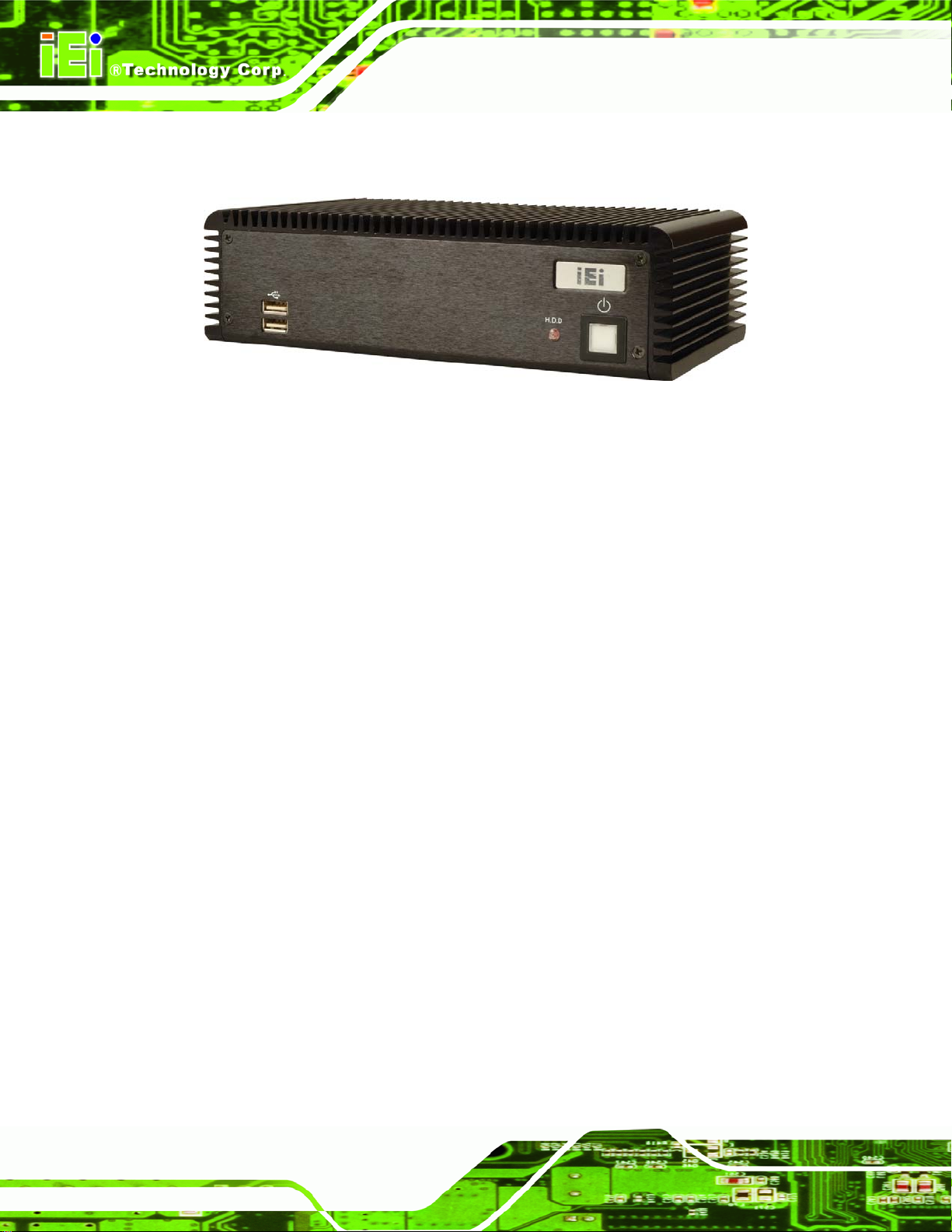
Figure 1-1: ECW-281B/281B2-R20 Series Embedded System
There are four WAFER-945GSE Intel® Atom™ based embedded solutions in the
ECW-281B Embedded System
ECW-281B/281B2-R20 series. All fanless motherboards have been optimized
multimedia applications that require minimum installation space. The WAFERmotherboard supports a full range of functions for an AT/ATX-compatible industrial computer.
ECW-281B/281B2-R20 embedded subsystems are all capable of supporting one 2.5” SATA
hard disk drive. The W models also have a built-in 802.11 b/g wireless module.
1.1.1 Benefits
The ECW-281B/281B2-R20 embedded system has the following benefits:
Easy installation saves installation time
Complete integration saves solution development time and cost
Secure storage with one SATA hard drive supported
Compact size saves space
Powerful preinstalled Intel® Atom™ N270 CPU and motherboard ensures
rigorous processing needs can be met
1.1.2 Features
for
945GSE
Page 2
The ECW-281B/281B2-R20 has the following features
RoHS compliant design
Fanless system
Built-in DC-to-DC power converter
Page 19
Page 3
1.6 GHz Intel® Atom™ N270 CPU supported
Dual GbE LAN for high speed network applications
One SATA hard drive supported
Wall mount and DIN mount supported.
1.2 Model Variations
There are six models in the ECW-281B/281B2-R20 embedded system series. The six
models are all preinstalled with an Intel® Atom™ N270 processor and 1 GB DDR2
memory. The model variations are listed in
684H684H684HTable 1-1 below.
ECW-281B Embedded System
ECW-281B Series Power Wireless VGA RS-232/422/485
ECW-281B-R20/N270/1GB 12V DC input
(60 W adaptor)
ECW-281BW-R20/N270/1GB 12V DC input
(60 W adaptor)
ECW-281BWD-R20/N270/1GB 9V~36V DC input No 1 x VGA 1 x RS-232/422/485
ECW-281BWDW-R20/N270/1GB 9V~36V DC input Yes 1 x VGA 1 x RS-232/422/485
ECW-281B2 Series Power Wireless VGA RS-232/422/485
ECW-281B2-R20/N270/1GB 12V DC input
(60 W adaptor)
ECW-281B2W-R20/N270/1GB 12V DC input
(60 W adaptor)
ECW-281B2WD-R20/N270/1GB 9V~36V DC input No 2 x VGA N/A
ECW-281B2WDW-R20/N270/1GB 9V~36V DC input Yes 2 x VGA N/A
No 1 x VGA 1 x RS-232/422/485
Yes 1 x VGA 1 x RS-232/422/485
No 2 x VGA N/A
Yes 2 x VGA N/A
Table 1-1: Model Variations
Page 20
ECW-281B Embedded System
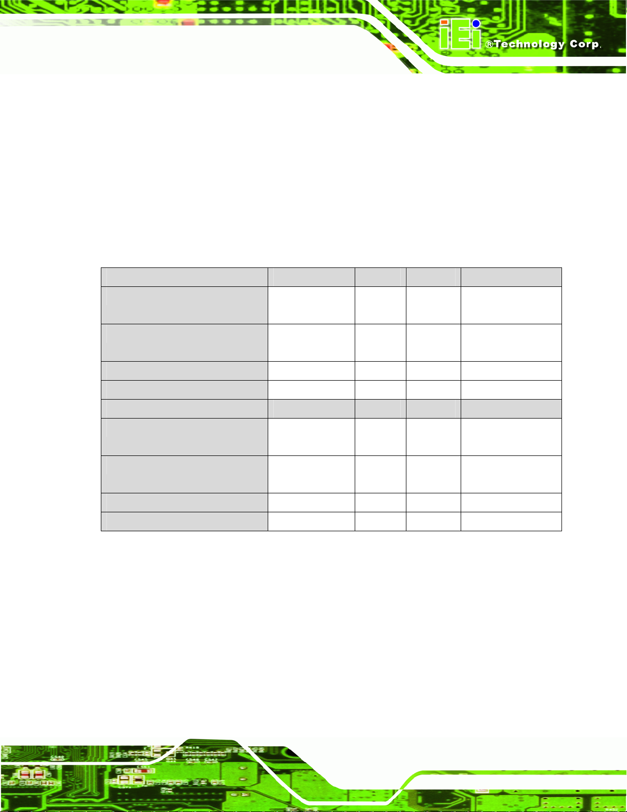
1.3 Technical Specifications
The specifications for the Intel based embedded systems are listed below.
ECW-281B-R20 ECW-281B2-R20
CPU
System Chipset
System Memory
Ethernet
Display
Serial Port
USB
Audio
Storage
Preinstalled 1.6 GHz Intel® Atom™ Processor N270 with a
533 MHz FSB
Intel® 945GSE + ICH7-M
Preinstalled 1.0 GB DDR2 SDRAM SO-DIMM (system max. 2 GB)
Dual Realtek RTL8111CP GbE controllers
Built-in 802.11 b/g wireless module for the wireless models
One VGA port Two VGA port
Five RS-232
One RS-232/422/485 (selectable)
Four USB 2.0 ports
One audio out
One 2.5” SATA hard drive supported
Five RS-232
Chassis Construction
Power Supply
Power Consumption
Operating Shock
Page 4
One internal CF card slot
Aluminum Alloy
Internal DC-to-DC power converter, input voltage:
12V DC or 9V – 36V (WD series models)
External power adapter, input voltage:
90V AC ~ 264V AC @ 47Hz ~ 63Hz, 60 W
19 W
Half-sine wave shock 3G; 11ms; 3 shocks per axis
Page 21
Page 5
ECW-281B Embedded System
Operating Vibration
Operating temperature
Color
Mounting
Weight (Net/Gross)
Dimensions (D x W x H)
EMC
Table 1-2: Technical Specifications
MIL-STD-810F 514.5C-1 (HDD)
MIL-STD-810F 514.5C-2 (CF)
-10ºC ~ 50ºC with HDD
-10ºC ~ 60ºC with CF card
Black
DIN mount
VESA MIS-D 100 wall mount
2.1 kg/3.9 kg
132 mm x 229 mm x 64 mm
FCC Class A, CE
1.4 Power Module Specifications
1.4.1 Power Module Options
The ECW-281B/281B2-R20 embedded system supports either a 12V DC input or a
9V~36V DC input. The input support depends on the power module installed in the system.
The two power modules are listed in
Embedded System Power Module DC Input
ECW-281B-R20 Series
ECW-281B2-R20 Series
ECW-281BWD-R20 Series
ECW-281B2WD-R20 Series
Table 1-3: ECW-281B/281B2-R20 Power Module Options
685H685H685HTable 1-3:
IDD-12250A 12V DC input
IDD-936260A 9V~36V DC input
Page 22
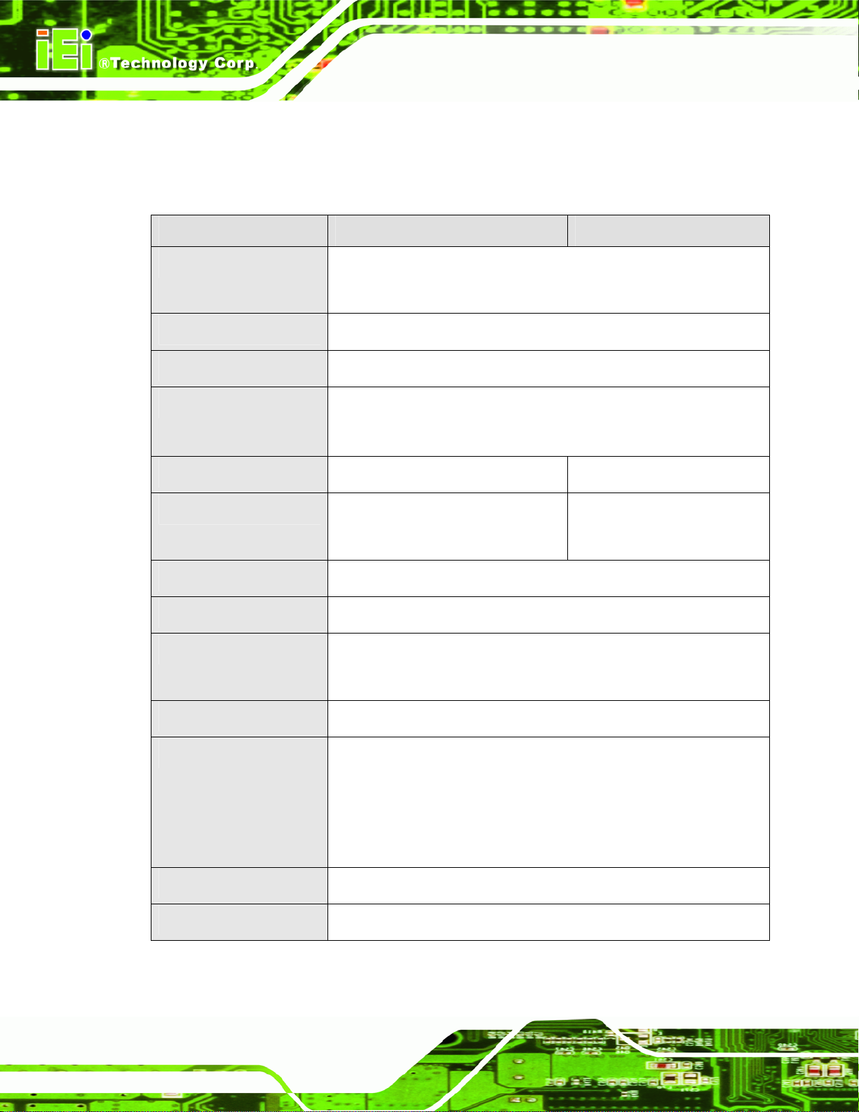
1.4.2 Power Module Specifications
The specifications for the IDD-12250A and IDD-936260A are shown in 686H686H686HTable 1-4.
Model Name: IDD-12250A IDD-936260A
ECW-281B Embedded System
Input
Output:
12V
5V
5VSB
Max. Total Output:
Performance Characteristics:
Noise & Ripple:
Line Regulation:
Load Regulation
Efficiency:
Dimensions:
12VDC 9VDC~36VDC
5A (pass thru.) 3A (Max.)
10A (Max.) 10A (Max.)
0.5A (Max.) 0.5A (Max.)
50W+60W (12V pass thru.) 60W
< 240mV < 240mV
< 20mV < 20mV
<60mV <60mV
Up to 90% Up to 90%
40mm x 100mm 40mm x 100mm
Page 6
Weight:
Operating Temperature:
Table 1-4: DC-to-DC Power Module Specifications
46g 58g
-40°C~85°C -40°C~85°C
Page 23
Page 7
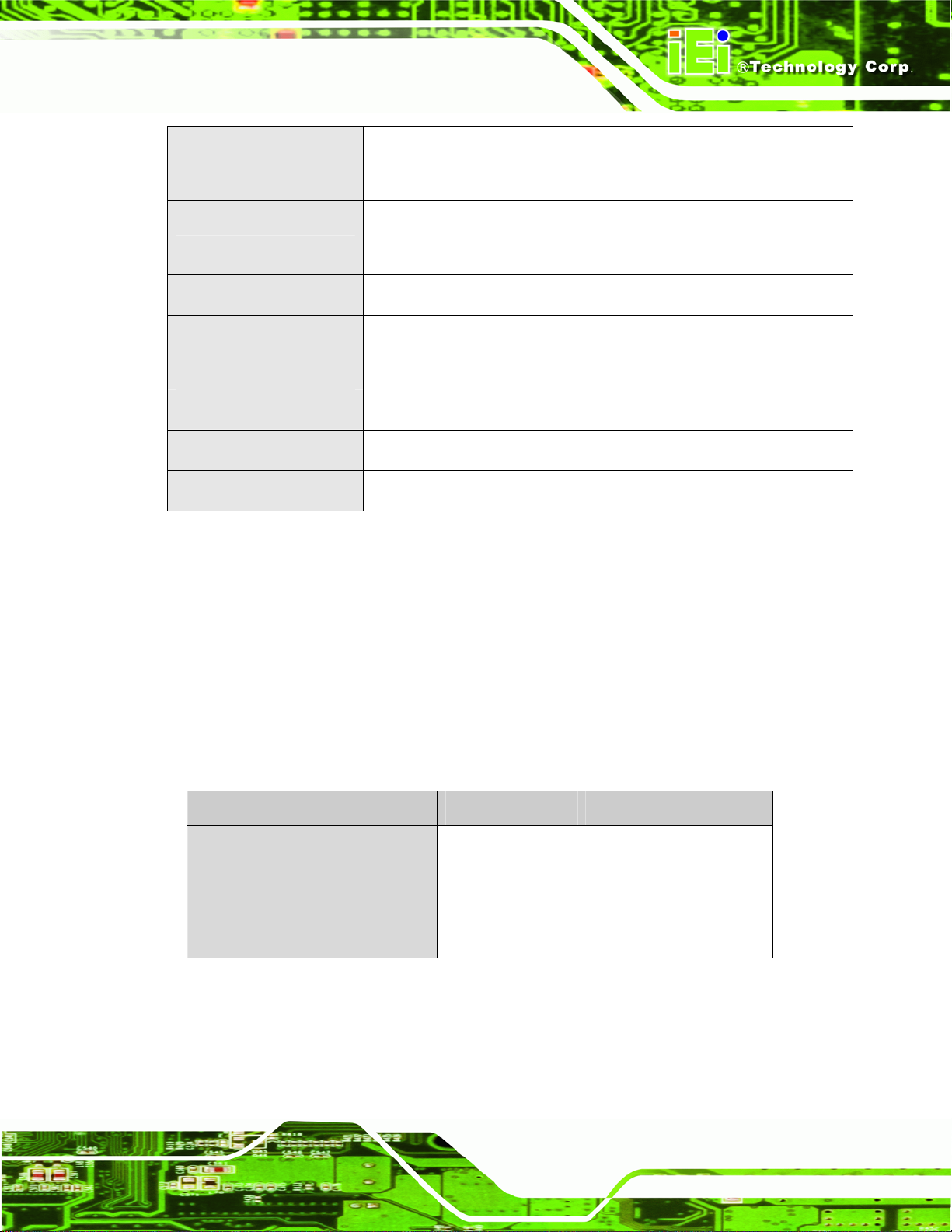
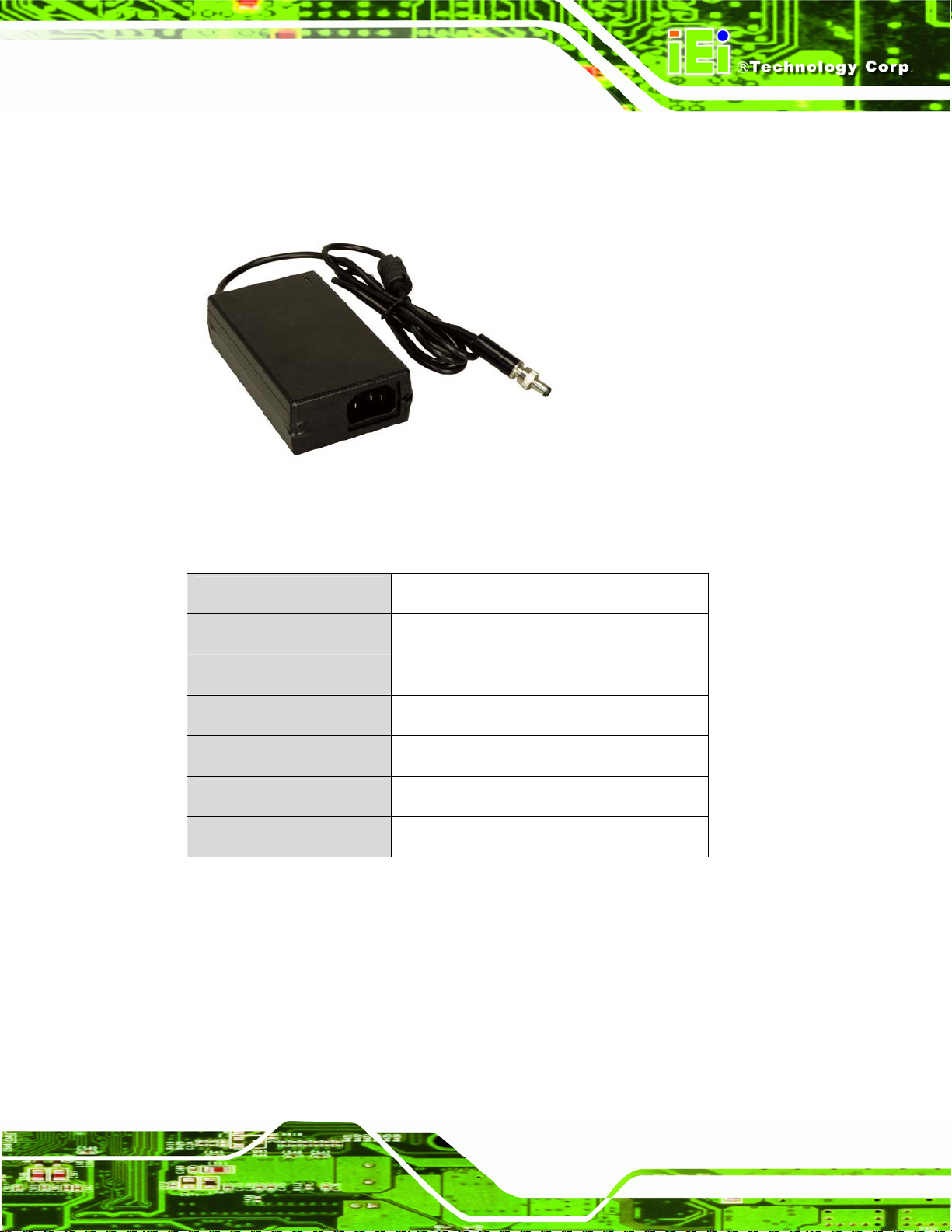
1.5 Power Adapter
The ECW-281B/281B2-R20 series models are shipped with a 60W power adapter.
ECW-281B Embedded System
Figure 1-2: Power Adapter
The specifications for the adapter are listed in
Input Voltage
Input Frequency
Output Voltage
Output Current
Efficiency
Operating Temperature
Storage Temperature
Table 1-5: Power Adapter Specifications
90 V ~ 264 V AC
47 Hz ~ 63 Hz
12 V
5 A
87%
0 ºC ~ 40 ºC
-20 ºC ~ 65 ºC
687H687H687HTable 1-5:
Page 24

ECW-281B Embedded System
Chapter
2
2 Mechanical Description
Page 8
Page 25

Page 9
2.1 Mechanical Overview
The ECW-281B/281B2-R20 RoHS compliant, Intel® Atom™ fanless embedded system
features industrial grade components that offer longer operating life, high shock/vibration
resistance and endurance over a wide temperature range. The ECW-281B/281B2-R20
combines these features in an aluminum enclosure designed for space critical
applications that require low power consumption. Featuring two LAN, four USB, six serial
communication ports, as well as audio, and VGA, the ECW-281B/281B2-R20 offers
system integrators and developers the best selection of robust and high performance
computing system platforms. An internal bracket supports one 2.5” SATA hard drives.
2.2 Physical Dimensions
The physical dimensions of the ECW-281B/281B2-R20 embedded systems are listed
below.
2.2.1 System Dimensions
The dimensions of the ECW-281B/281B2-R20 are listed below and shown in 688H688H688HFigure 2-1.
Height: 64.00 mm
Width: 229.00 mm
Length: 132.00 mm
ECW-281B Embedded System
Page 26
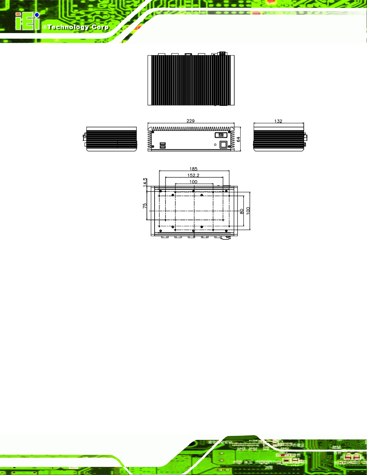
ECW-281B Embedded System
Figure 2-1: ECW-281B/281B2-R20 Dimensions (mm)
2.2.2 Motherboard Dimensions
The WAFER series dimension are listed below and shown in 689H689H689HFigure 2-2.
Length: 145.00 mm
Width: 102.00 mm
Page 10
Page 27
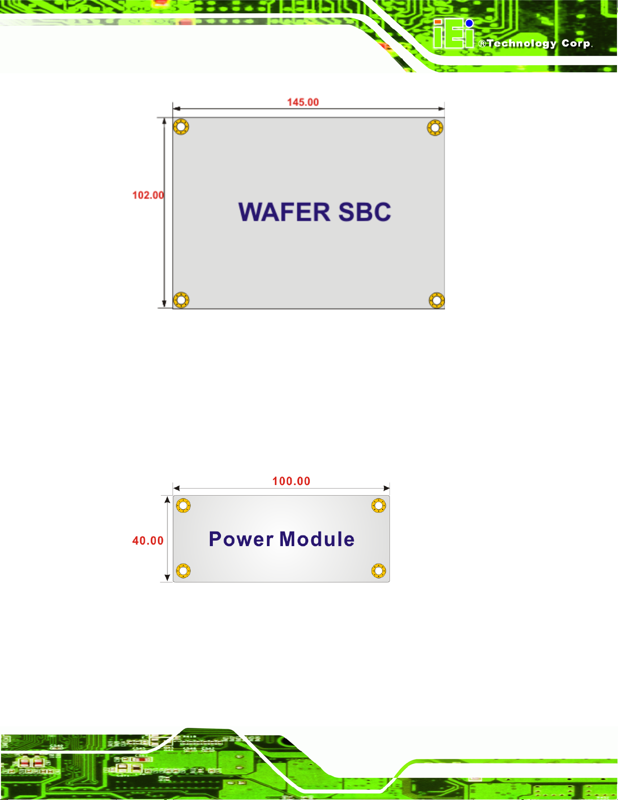
Page 11
Figure 2-2: WAFER SBC Dimensions (mm)
2.2.3 Power Module Dimensions
The power module dimensions are listed below and shown in 690H690H690HFigure 2-3.
Length: 100.00 mm
Width: 40.00 mm
Figure 2-3: Power Module Dimensions (mm)
ECW-281B Embedded System
Page 28
2.3 External Overview
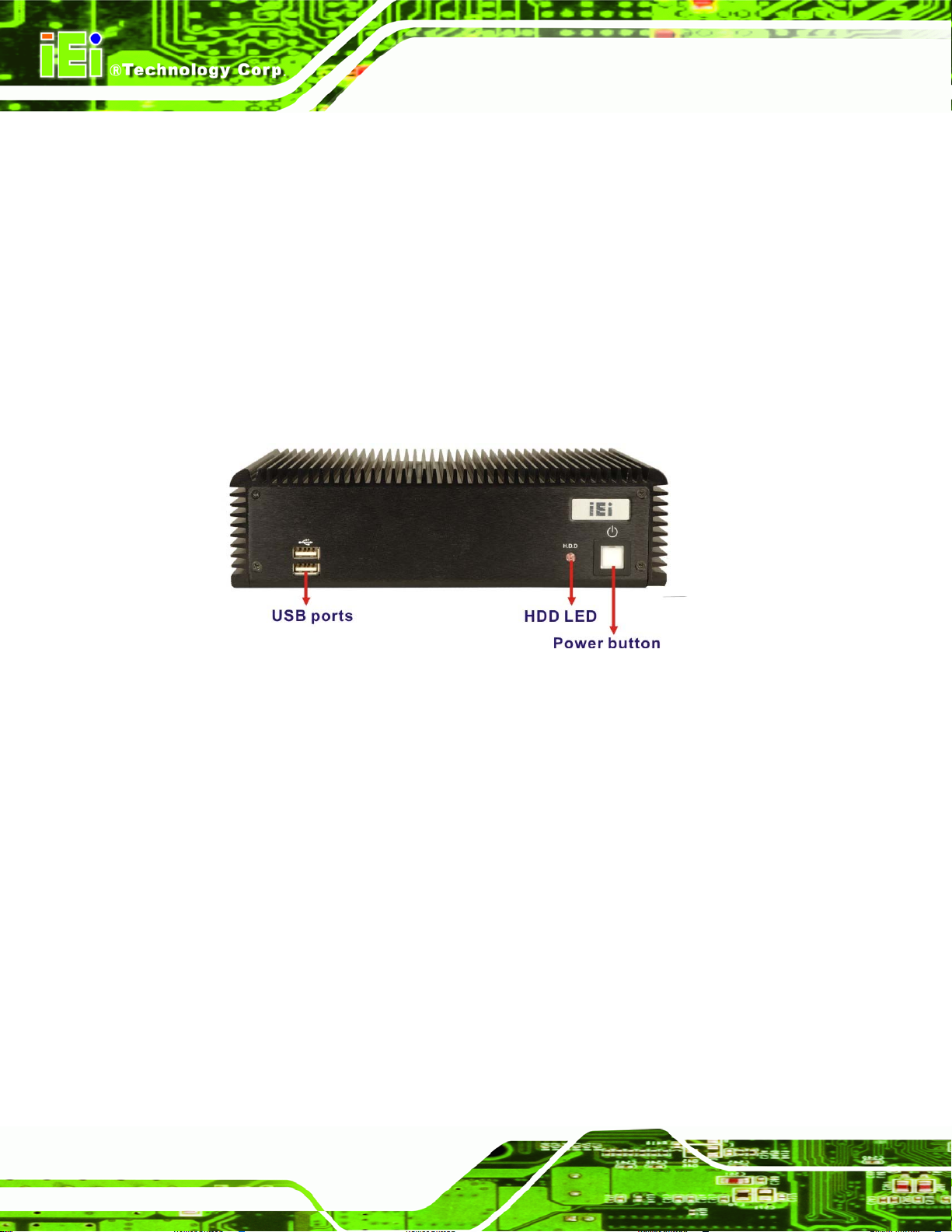
2.3.1 Front Panel
The ECW-281B/281B2-R20 front panel contains:
2 x USB port connectors
1 x HDD LED indicator
1 x Power button
ECW-281B Embedded System
An overview of the front panel is shown in
691H691H691HFigure 2-4 below.
Figure 2-4: ECW-281B/281B2-R20 Front Panel
2.3.2 Rear Panel
2.3.2.1 ECW-281B-R20 Rear Panel
The rear panel of the ECW-281B-R20 provides access to the following external I/O
connectors.
Page 12
2 x USB port connectors
2 x RJ-45 Ethernet connector
1 x VGA connector
1 x RS-232/422/485 serial port
5 x RS-232 serial ports
1 x Speaker out
1 x 3-pin power terminal block
1 x 12V DC power jack
Page 29
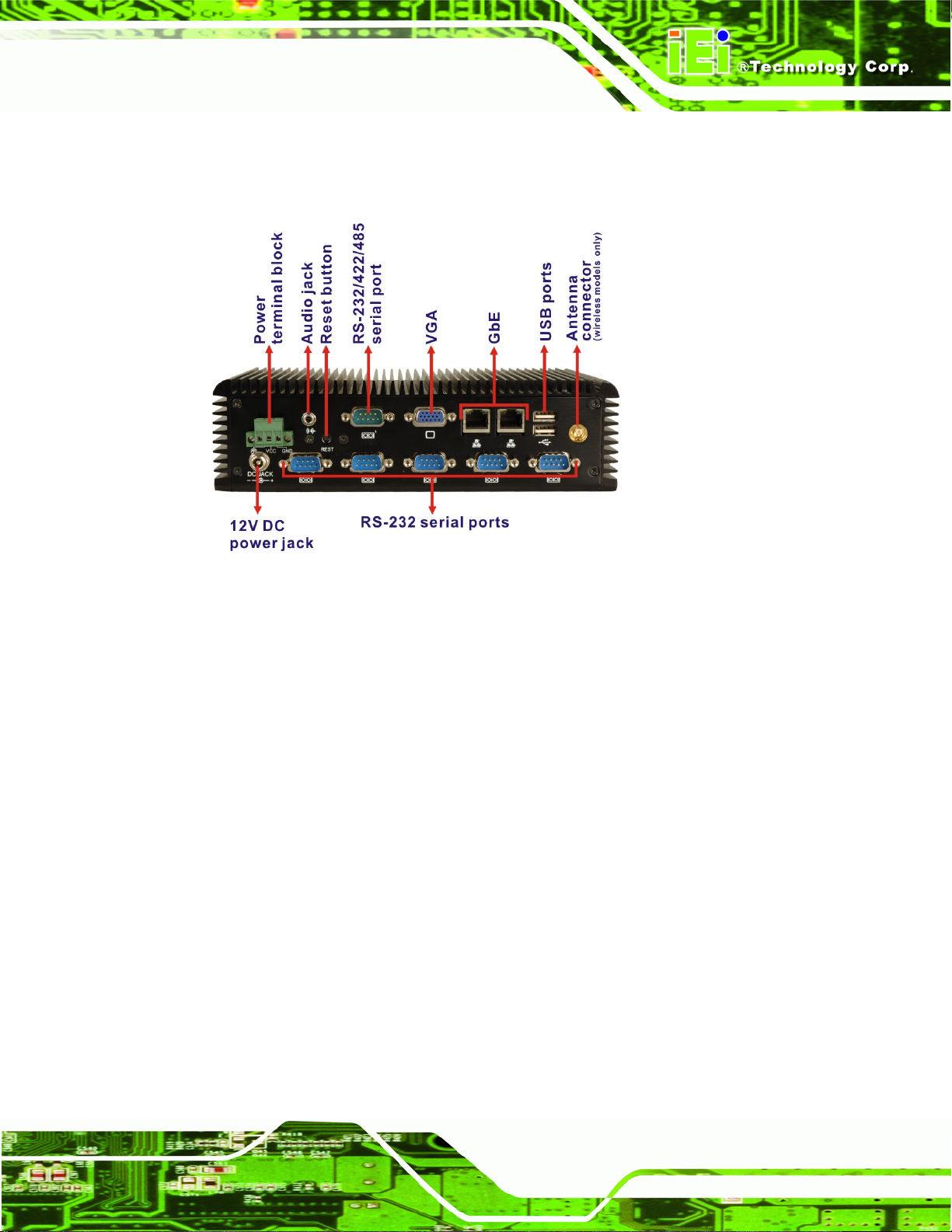
Page 13
1 x Wireless antenna connector (for wireless models only)
An overview of the rear panel is shown in
692H692H692HFigure 2-5.
Figure 2-5: ECW-281B/281B2-R20 Rear Panel
2.3.2.2 ECW-281B2-R20 Rear Panel
The rear panel of the ECW-281B2-R20 provides access to the following external I/O
connectors.
2 x USB port connectors
2 x RJ-45 Ethernet connector
2 x VGA connectors
5 x RS-232 serial ports
1 x Speaker out
1 x 3-pin power terminal block
1 x 12V DC power jack
1 x Wireless antenna connector (for wireless models only)
An overview of the rear panel is shown in
693H693H693HFigure 2-6.
ECW-281B Embedded System
Page 30
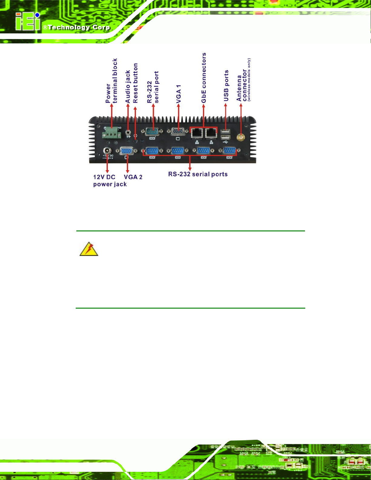
ECW-281B Embedded System
Figure 2-6: ECW-281B/281B2-R20 Rear Panel
2.3.3 Bottom Surface
WARNING:
Never remove the bottom access panel from the chassis while power is still
being fed into the system. Before removing the bottom access panel, make
sure the system has been turned off and all power connectors unplugged.
The bottom surface of the ECW-281B/281B2-R20 contains the retention screw holes for
the VESA MIS-D 100 wall-mount kit, two-side mounting brackets and DIN mount bracket.
Page 14
Page 31

Page 15
Figure 2-7: Bottom Surface
2.4 Internal Overview
The ECW-281B/281B2-R20 internal components are listed below:
1 x IEI WAFER motherboard (preinstalled)
1 x IEI power module (preinstalled)
1 x SO-DIMM module (preinstalled)
1 x Hard drive bracket and SATA cable support one SATA hard disk
All the components are accessed by removing the bottom surface.
ECW-281B Embedded System
Page 32

ECW-281B Embedded System
Figure 2-8: Internal Overview
Page 16
Page 33

Page 17
Chapter
3
3 System Components
ECW-281B Embedded System
Page 34

3.1 Embedded System Motherboard
NOTE:
The jumpers and connectors shown in the section below are those jumpers
and connectors that are relevant to the configuration and installation of the
embedded system. For a complete list of jumpers and connectors on the
WAFER-945GSE motherboard, please refer to the WAFER-945GSE user
manual.
The ECW-281B/281B2-R20 models have a WAFER-945GSE motherboard installed in the
system. The following sections describe the relevant connectors and jumpers on the
motherboard.
ECW-281B Embedded System
3.1.1 WAFER-945GSE Motherboard Overview
The locations of the WAFER-945GSE jumpers and connectors used on the
ECW-281B/281B2-R20 are shown in
694H694H694HFigure 3-1 below.
Page 18
Figure 3-1: WAFER-945GSE Jumper and Connector Locations
Page 35

Page 19
3.1.2 CPU Support
NOTE:
The ECW-281B/281B2-R20 series has a preinst alled Intel® Atom™ 1.6
GHz CPU on-board. If the CPU fails, the motherboard has to be
replaced. Please contact the IEI reseller or vendor you purchased the
ECW-281B/281B2-R20 from or contact an IEI sales representative
directly. To contact an IEI sales representative, please send an email to
300H300H300Hsales@iei.com.tw.
The ECW-281B/281B2-R20 comes with an embedded 45 nm 1.60 GHz Intel® Atom™
processor N270. The processor supports a 533 MHz FSB and has a 1.6 GHz 512 KB L2
cache. The low power processor has a maximum power of 2.5 W.
3.2 Peripheral Interface Connectors
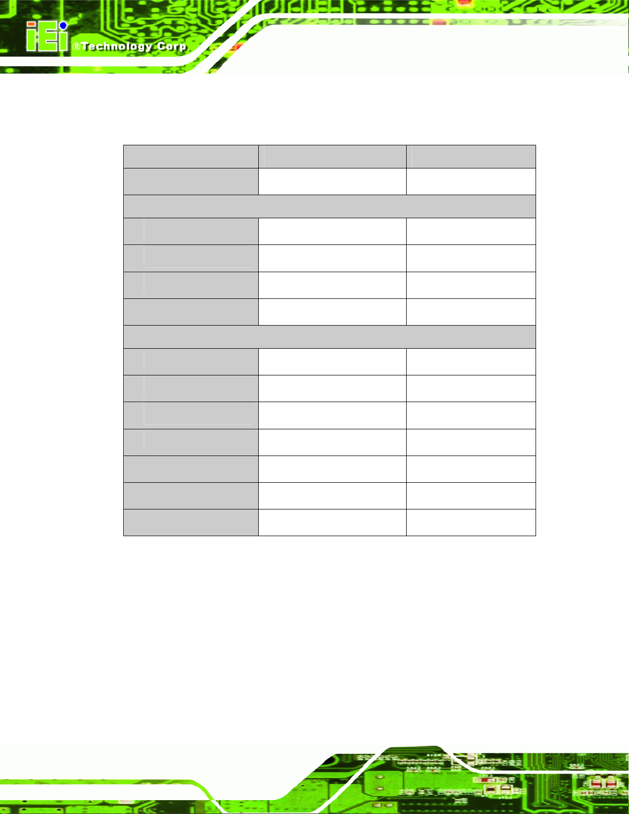
Section 695H695H695H3.2.1 lists all the peripheral interface connectors seen in Section 696H696H696H3.1.1.
3.2.1 Peripheral Interface Connectors
697H697H697HTable 3-1 shows a list of the peripheral interface connectors on the WAFER-945GSE that
are used for the ECW-281B/281B2-R20. Detailed descriptions of these connectors can be
found in Section
698H698H698H3.3.
ECW-281B Embedded System
Connector Type Label
Audio connector 10-pin header AUDIO1
ATX enable connector 3-pin wafer ATXCTL1
ATX power connector 4-pin ATX ATXPWR1
CompactFlash® socket 50-pin CF socket CF1
LED connector 6-pin header LED_C1
Page 36

ECW-281B Embedded System
PCIe Mini Card slot PCIe Mini Slot CN4
Power Button 2-pin wafer PWRBTN1
Reset button connector 2-pin header RESET1
Serial ATA (SATA) drive connectors 7-pin SATA SATA1
RS-232 serial port connector (COM3 – COM6) 40-pi n header COM
RS-232/422/485 serial port connector 14-pin header COM2
USB 2.0 connector 8-pin header USB01
Table 3-1: Peripheral Interface Connectors
3.3 Internal Peripheral Connectors
Internal peripheral connectors are found on the motherboard and are only accessible
when the motherboard is outside of the chassis. T his se ction h as complet e d esc ription s of
the internal, peripheral connectors on the WAFER-945GSE that are used for the
ECW-281B/281B2-R20.
3.3.1 ATX Power Connector
CN Label:
CN Type:
CN Location:
CN Pinouts:
ATXPWR1
4-pin AT power connector (1x4)
699H699H699HFigure 3-2
See
700H700H700HTable 3-2
See
Page 20
The 4-pin ATX power connector is connected to a DC-DC power module.
Page 37

Page 21
ECW-281B Embedded System
Figure 3-2: ATX Power Connector Location
PIN NO. DESCRIP TIO N
1 +12V
2 GND
3 GND
4 +5V
Table 3-2: ATX Power Connector Pinouts
3.3.2 ATX Power Supply Enable Connector
CN Label:
CN Type:
CN Location:
CN Pinouts:
The ATX power supply enable connector is connected to the ATX mode connector on the
power module to enable the ECW-281B/281B2-R20 to be connected to an ATX power
supply.
ATXCTL1
3-pin wafer (1x3)
701H701H701HFigure 3-3
See
702H702H702HTable 3-3
See
Page 38

ECW-281B Embedded System
Figure 3-3: ATX Power Supply Enable Connector Location
PIN NO. DESCRIP TIO N
1 +5V Standby
2 GND
3 PS-ON
Table 3-3: ATX Power Supply Enable Connector Pinouts
3.3.3 Audio Connector (10-pin)
CN Label:
CN Type:
CN Location:
CN Pinouts:
The 10-pin audio connector is interfaced to an audio line-out connector and provides
output of audio signals from the system.
AUDIO1
10-pin header
703H703H703HFigure 3-4
See
704H704H704HTable 3-4
See
Page 22
Figure 3-4: Audio Connector Pinouts (10-pin)
Page 39

Page 23
PIN NO. DESCRIPTION PIN NO. DESCRIPTION
1 Line out R 2 Line in R
3 GND 4 GND
5 Line out L 6 Line in L
7 GND 8 GND
9 MIC in 10 Mic in
Table 3-4: Audio Connector Pinouts (10-pin)
3.3.4 CompactFlash® Socket
CN Label:
CF1
CN Type:
50-pin header (2x25)
CN Location:
See
705H705H705HFigure 3-5
CN Pinouts:
See
706H706H706HTable 3-5
A CF Type I or Type II memory card is inserted to the CF socket on the solder side of the
ECW-281B/281B2-R20.
ECW-281B Embedded System
Figure 3-5: CF Card Socket Location
Page 40

ECW-281B Embedded System
PIN NO. DESCRIPTION PIN NO. DESCRIPTION
1 GROUND 26 VCC-IN CHECK1
2 DATA 3 27 DATA 11
3 DATA 4 28 DATA 12
4 DATA 5 29 DATA 13
5 DATA 6 30 DATA 14
6 DATA 7 31 DATA 15
7 HDC_CS0# 32 HDC_CS1
8 GROUND 33 N/C
9 GROUND 34 IOR#
10 GROUND 35 IOW#
11 GROUND 36 VCC_COM
12 GROUND 37 IRQ14
13 VCC_COM 38 VCC_COM
14 GROUND 39 CSEL
15 GROUND 40 N/C
16 GROUND 41 HDD_RESET
17 GROUND 42 IORDY
18 SA2 43 SDREQ
19 SA1 44 SDACK#
20 SA0 45 HDD_ACTIVE#
21 DATA 0 46 66DET
22 DATA 1 47 DATA 8
23 DATA 2 48 DATA 9
24 N/C 49 DATA 10
25 VCC-IN CHECK2 50 GROUND
Table 3-5: CF Card Socket Pinouts
3.3.5 LED Connector
Page 24
CN Label:
CN Type:
LED_C1
6-pin wafer (1x6)
Page 41

Page 25
CN Location:
See
707H707H707HFigure 3-6
CN Pinouts:
See
708H708H708HTable 3-6
The LED connector connects to an HDD indicator LED and a power LED on the system
chassis to inform the user about HDD activity and the power on/off status of the system.
ECW-281B Embedded System
Figure 3-6: LED Connector Locations
PIN NO. DESCRIPTION
1 +5V
2 GND
3 Power LED+
4 Power LED5 HDD LED+
6 HDD LED-
Table 3-6: LED Connector Pinouts
3.3.6 PCIe Mini Card Slot
CN Label:
CN Type:
CN Location:
CN Pinouts:
The PCIe mini card slot enables a PCIe mini card expansion module to be connected to
CN4
52-pin Mini PCIe Card Slot
791H709H709H709HFigure 3-7
See
710H710H710HTable 3-7
See
the board. Cards supported include among others wireless LAN (WLAN) cards.
Page 42

ECW-281B Embedded System
Figure 3-7: PCIe Mini Card Slot Location
PIN NO. DESCRIPTION PIN NO. DESCRIPTION
1 PCIE_WAKE# 2 VCC3
3 N/C 4 GND
5 N/C 6 1.5V
7 CLKREQ# 8 LFRAME#
9 GND 10 LAD3
11 CLK- 12 LAD2
13 CLK+ 14 LAD1
15 GND 16 LAD0
17 PCIRST# 18 GND
19 LPC 20 VCC3
21 GND 22 PCIRST#
23 PERN2 24 3VDual
25 PERP2 26 GND
27 GND 28 1.5V
Page 26
29 GND 30 SMBCLK
31 PETN2 32 SMBDATA
33 PETP2 34 GND
35 GND 36 USBD37 N/C 38 USBD+
39 N/C 40 GND
Page 43

Page 27
41 N/C 42 N/C
43 N/C 44 RF_LINK#
45 N/C 46 BLUELED#
47 N/C 48 1.5V
49 N/C 50 GND
51 N/C 52 VCC3
Table 3-7: PCIe Mini Card Slot Pinouts
3.3.7 Power Button Connector
CN Label:
PWRBTN1
CN Type:
2-pin wafer (1x2)
CN Location:
See
711H711H711HFigure 3-8
CN Pinouts:
See
712H712H712HTable 3-8
The power button connector is connected to a power switch on the system chassis to
enable users to turn the system on and off.
ECW-281B Embedded System
Figure 3-8: Power Button Connector Location
PIN NO. DESCRIPTION
1 Power Switch
2 GND
Table 3-8: Power Button Connector Pinouts
Page 44

3.3.8 Reset Button Connector
ECW-281B Embedded System
CN Label:
CN Type:
CN Location:
CN Pinouts:
RESET1
2-pin wafer (1x2)
713H713H713HFigure 3-9
See
714H714H714HTable 3-9
See
The reset button connector is connected to a reset switch o n the syst em chassi s to enabl e
users to reboot the system when the system is turned on.
Figure 3-9: Reset Button Connector Locations
PIN NO. DESCRIPTION
1 Reset Switch
2 GND
Table 3-9: Reset Button Connector Pinouts
3.3.9 SATA Drive Connectors
Page 28
CN Label:
CN Type:
CN Location:
CN Pinouts:
SA TA1, SATA2
7-pin SATA drive connectors
See
See
793H715H715H715HFigure 3-10
794H716H716H716HTable 3-10
Page 45

Page 29
The SATA drive connectors are each connected to a first generation SATA drive. First
generation SATA drives transfer data at speeds as high as 150Mb/s. The SATA drives can
be configured in a RAID configuration.
Figure 3-10: SATA Drive Connector Locations
PIN NO.
ECW-281B Embedded System
DESCRIPTION
1 GND
2 TX+
3 TX4 GND
5 RX6 RX+
7 GND
Table 3-10: SATA Drive Connector Pinouts
3.3.10 Serial Port Connector (COM3, COM4, COM5 and COM6)
CN Label:
CN Type:
CN Location:
CN Pinouts:
COM
40-pin header (2x20)
717H717H717HFigure 3-11
See
718H718H718HTable 3-11
See
Page 46

ECW-281B Embedded System
The 40-pin serial port connector contains the following four serial ports: COM3, COM4,
COM5 and COM6. All these serial ports are RS-232 serial communications channels. The
serial port locations are specified below.
COM3 is located on pin 1 to pin 10
COM4 is located on pin 11 to pin 20
COM5 is located on pin 21 to pin 30
COM6 is located on pin 31 to pin 40
Figure 3-11: COM3 to COM6 Connector Pinout Locations
PIN NO. DESCRIPTION PIN NO. DESCRIPTION
Page 30
1 DATA CARRIER DETECT (DCD3) 2 DATA SET READY (DSR3)
3 RECEIVE DATA (RXD3) 4 REQUEST TO SEND (RTS3)
5 TRANSMIT DATA (TXD3) 6 CLEAR TO SEND (CTS3)
7 DATA TERMINAL READY (DTR3) 8 RING INDICATOR (RI3)
9 GND 10 GND
11 DATA CARRIER DETECT (DCD4) 12 DATA SET READY (DSR4)
13 RECEIVE DATA (RXD4) 14 REQUEST TO SEND (RTS4)
15 TRANSMIT DATA (TXD4) 16 CLEAR TO SEND (CTS4)
17 DATA TERMINAL READY (DTR4) 18 RING INDICATOR (RI4)
19 GND 20 GND
Page 47

Page 31
PIN NO. DESCRIPTION PIN NO. DESCRIPTION
21 DATA CARRIER DETECT (DCD5) 22 DATA SET READY (DSR5)
23 RECEIVE DATA (RXD5) 24 REQUEST TO SEND (RTS5)
25 TRANSMIT DATA (TXD5) 26 CLEAR TO SEND (CTS5)
27 DATA TERMINAL READY (DTR5) 28 RING INDICATOR (RI5)
29 GND 30 GND
31 DATA CARRIER DETECT (DCD6 32 DATA SET READY (DSR6)
33 RECEIVE DATA (RXD6) 34 REQUEST TO SEND (RTS6)
35 TRANSMIT DATA (TXD6 36 CLEAR TO SEND (CTS6)
37 DATA TERMINAL READY (DTR6 38 RING INDICATOR (RI6)
39 GND 40 GND
Table 3-11: COM3 to COM6 Connector Pinouts
3.3.11 Serial Port Connector (COM 2)(RS-232, RS-422 or RS-485)
CN Label:
COM2
CN Type:
14-pin header (2x7)
CN Location:
See
719H719H719HFigure 3-12
CN Pinouts:
See
720H720H720HTable 3-12
The 14-pin serial port connector connects to the COM2 serial communications channels.
COM2 is a multi function channel. In default mode COM2 is an RS-232 serial
communication channel but, with the COM2 function select jumper, can be configured as
either an RS-422 or RS-485 serial communications channel.
ECW-281B Embedded System
Page 48

ECW-281B Embedded System
Figure 3-12: RS-232/422/485 Serial Port Connector Location
PIN NO. DESCRIPTION PIN NO. DESCRIPTION
1 NDCD 2 NDSR2
3 NRX 4 NRTS2
5 NTX 6 NCTS2
7 NDTR 8 NRI2
9 GND 10 GND
11 TXD485+ 12 TXD48513 RXD485+ 14 RXD485-
Table 3-12: RS-232/RS-485 Serial Port Connector Pinouts
3.3.12 USB Connectors (Internal)
CN Label:
CN Type:
CN Location:
CN Pinouts:
The 2x4 USB pin connectors each provide connectivity to two USB 1.1 or two USB 2.0
USB01 and USB23
8-pin header (2x4)
801H721H721H721HFigure 3-13
See
802H722H722H722HTable 3-13
See
Page 32
ports. Each USB connector can support two USB devices. Additional external USB ports
are found on the rear panel. The USB ports are used for I/O bus expansion.
Page 49

Page 33
ECW-281B Embedded System
Figure 3-13: USB Connector Pinout Locations
PIN NO. DESCRIPTION PIN NO. DESCRIPTION
1 VCC 2 GND
3 DATA- 4 DATA+
5 DATA+ 6 DATA7 GND 8 VCC
Table 3-13: USB Port Connector Pinouts
3.4 External Peripheral Interface Connector Panel
803H723H723H723HFigure 3-14 shows the ECW-281B/281B2-R20 external peripheral interface connector
(EPIC) panel. The ECW-281B/281B2-R20 EPIC panel consists of the following:
2 x RJ-45 LAN connectors
1 x Serial port connectors
2 x USB connectors
1 x VGA connector
Page 50

Figure 3-14: ECW-281B/281B2-R20 External Peripheral Interface Connector
3.4.1 LAN Connectors
ECW-281B Embedded System
CN Label:
CN Type:
CN Location:
CN Pinouts:
LAN1 and LAN2
RJ-45
808H724H724H724HFigure 3-14
See
809H725H725H725HTable 3-14
See
The ECW-281B/281B2-R20 is equipped with two built-in RJ-45 Ethernet controllers. The
controllers can connect to the LAN through two RJ-45 LAN connectors. There are two
LEDs on the connector indicating the status of LAN. The pin assignments are listed in the
following table:
PIN DESCRIPTION PIN
1 MDIA3- 5 MDIA1+
2 MDIA3+ 6 MDIA2+
3 MDIA2- 7 MDIA04 MDIA1- 8 MDIA0+
DESCRIPTION
Table 3-14: LAN Pinouts
Figure 3-15: RJ-45 Ethernet Connector
Page 34
Page 51

Page 35
The RJ-45 Ethernet connector has two status LEDs, one green and one yello w. The green
LED indicates activity on the port and the yellow LED indicates the port is linked. See
810H726H726H726HTable 3-15.
ECW-281B Embedded System
STATUS
GREEN Activity YELLOW Linked
DESCRIPTION STATUS DESCRIPTION
Table 3-15: RJ-45 Ethernet Connector LEDs
3.4.2 Serial Port Connector (COM1)
CN Label:
CN Type:
CN Location:
CN Pinouts:
The 9-pin DB-9 serial port connectors are connected to RS-232 serial communications
devices.
PIN NO. DESCRIPTION PIN NO. DESCRIPTION
1 DCD 6 DSR
COM1
DB-9 connectors
811H727H727H727HFigure 3-14
See
812H728H728H728HTable 3-16 and 813H729H729H729HFigure 3-16
See
2 RX 7 RTS
3 TX 8 CTS
4 DTR 9 RI
5 GND
Table 3-16: RS-232 Serial Port (COM 1) Pinouts
Figure 3-16: COM1 Pinout Locations
Page 52

3.4.3 USB Connectors
CN Label: USB
ECW-281B Embedded System
CN T ype:
CN Location: See
CN Pinouts: See
Dual USB port
814H730H730H730HFigure 3-14
815H731H731H731HTable 3-17
The ECW-281B/281B2-R20 has two external USB 2.0 ports. The ports connect to both
USB 2.0 and USB 1.1 devices.
PIN NO. DESCRIPTION PIN NO. DESCRIPTION
1 VCC 5 VCC
2 DATA- 6 DATA3 DATA+ 7 DATA+
4 GND 8 GND
Table 3-17: USB Port Pinouts
3.4.4 VGA Connector
CN Label:
CN Type:
CN Location:
CN Pinouts:
VGA1
15-pin Female
816H732H732H732HFigure 3-14
See
817H733H733H733HFigure 3-17 and 818H734H734H734HTable 3-18
See
The single 15-pin female connector for connectivity to standard display devices.
Figure 3-17: VGA Connector
Page 36
Page 53

Page 37
PIN DESCRIPTION PIN DESCRIPTION
1 RED 2 GREEN
3 BLUE 4 NC
5 GND 6 CRT_PLUG7 GND 8 GND
9 VCC 10 GND
11 NC 12 DDC DAT
13 HSYNC 14 VSYNC
15 DDCCLK
Table 3-18: VGA Connector Pinouts
3.5 WAFER-945GSE Motherboard On-board Jumpers
NOTE:
A
ECW-281B Embedded System
jumper is a metal bridge used to close
an electrical circuit. It consists of two or
three metal pins and a small metal clip
(often protected by a plastic cover) that
slides over the pins to connect them. To
CLOSE/SHORT a jumper means
connecting the pins of the jumper with
the plastic clip and to OPEN a jumper
means removing the plastic clip from a
jumper.
The WAFER-945GSE motherboard has several onboard jumpers (735H735H735HTable 3-19).
Description Label Type
CF Card Setting JCF1 2-pin header
Figure 3-18: Jumpers
Clear CMOS J_CMOS1 3-pin header
Page 54

COM2 Mode Setting JP1 6-pin header
Table 3-19: Jumpers
3.5.1 CF Card Setup
ECW-281B Embedded System
Jumper Label:
Jumper Type:
Jumper Settings:
Jumper Location:
JCF1
2-pin header
736H736H736HTable 3-20
See
737H737H737HFigure 3-19
See
The CF Card Setup jumper sets the CF Type I card or CF Type II cards as either the slave
device or the master device. CF Card Setup jumper settings are shown in
CF Card Setup Description
OFF Slave Default
Short 1-2 Master
738H738H738HTable 3-20.
Table 3-20: CF Card Setup Jumper Settings
The CF Card Setup jumper location is shown in 739H739H739HFigure 3-19.
Figure 3-19: CF Card Setup Jumper Location
3.5.2 Clear CMOS Jumper
Jumper Label:
Jumper Type:
Page 38
J_CMOS1
3-pin header
Page 55

Page 39
Jumper Settings:
See
830H740H740H740HTable 3-21
Jumper Location:
See
831H741H741H741HFigure 3-20
If the ECW-281B/281B2-R20 fails to boot due to improper BIOS settings, the clear CMOS
jumper clears the CMOS data and resets the system BIOS information. To do this, use the
jumper cap to close pins 2 and 3 for a few seconds then reinstall the jumper clip back to
pins 1 and 2.
If the “CMOS Settings Wrong” message is displayed during the boot up process, the fault
may be corrected by pressing the F1 to enter the CMOS Setup menu. Do one of the
following:
Enter the correct CMOS setting
Load Optimal Defaults
Load Failsafe Defaults.
After having done one of the above, save the changes and exit the CMOS Setup menu.
The clear CMOS jumper settings are shown in
832H742H742H742HTable 3-21.
ECW-281B Embedded System
AT Power Select Description
Short 1 - 2 Keep CMOS Setup Default
Short 2 - 3 Clear CMOS Setup
Table 3-21: Clear CMOS Jumper Settings
The location of the clear CMOS jumper is shown in 833H743H743H743HFigure 3-20 below.
Figure 3-20: Clear CMOS Jumper
Page 56

ECW-281B Embedded System
3.5.3 COM 2 Function Select Jumper (ECW-281B-R20 Series Only)
Jumper Label:
Jumper Type:
Jumper Settings:
Jumper Location:
JP1
8-pin header
744H744H744HTable 3-22
See
745H745H745HFigure 3-21
See
The COM 2 Function Select jumper sets the communication protocol used by the second
serial communications port (COM 2) as RS-232, RS-422 or RS -485. The COM 2 Function
Select settings are shown in
COM 2 Function Select Description
Short 1-2 RS-232 Default
Short 3-4 RS-422
Short 5-6 RS-485
Short 5-6
Short 7-8
746H746H746HTable 3-22.
RS-485 with RTS control
Table 3-22: COM 2 Function Select Jumper Settings
The COM 2 Function Select jumper location is shown in 747H747H747HFigure 3-21.
Figure 3-21: COM 2 Function Select Jumper Location
Page 40
Page 57

Page 41
3.6 Connector Mappings
This section describes how the connectors on the motherboard and power module are
connected to different components within the system. When performing maintenance
operations on the system it is imperative that the correct connections are made.
3.6.1 Power Connector
The connector mapping for the power module output power connector and the
motherboard input power connector are shown in
748H748H748HTable 3-23.
ECW-281B Embedded System
WAFER-945GSE Power Module
ATXPWR1: Power CN4: Output Power
Pin 1 Pin 4
Pin 2 Pin 3
Pin 3 Pin 2
Pin 4 Pin 1
Table 3-23: Motherboard Power Connector Mapping
3.6.2 ATX Mode Connector
The connector mapping for the ATX mode connector on the motherboard and power
module are shown in
WAFER-945GSE Power Module
ATXCTL1: PS-ON CN7: ATX Mode
749H749H749HTable 3-24.
Pin 1 Pin 1
Pin 2 Pin 2
Pin 3 Pin 3
Table 3-24: Motherboard Power Connector Mapping
Page 58

ECW-281B Embedded System
Chapter
4
4 Installation
Page 42
Page 59

Page 43
4.1 Anti-static Precautions
WARNING:
If the following anti-static precautions are not followed, a user may be
injured and the system irreparably damaged.
Electrostatic discharge (ESD) can cause serious damage to electronic components,
including the WAFER series motherboard and the power module. (Dry climates are
especially susceptible to ESD.) It is therefore critical that whenever the
ECW-281B/281B2-R20 is opened and any electrical component handled, the following
anti-static precautions are strictly adhered to.
Wear an anti-static wristband: - Wearing a simple anti-static wristband can
help to prevent ESD from damaging the board.
Self-grounding:- Before handling the board, touch any grounded conducting
material. During the time the board is handled, frequently touch any
conducting materials that are connected to the ground.
4.2 Installation Procedure
4.2.1 Installation Procedure Overview
To properly install the ECW-281B/281B2-R20, the following steps must be followed.
Detailed descriptions of these instructions are listed in the sections that follow.
Step 1: Unpacking
Step 2: Configure the jumper settings
Step 3: Install the SA TA hard disk drive (HDD)
Step 4: Mount the ECW-281B/281B2-R20
Step 5: Connect the front panel peripheral connectors
ECW-281B Embedded System
Page 60

Step 6: Power the system upStep 0:
4.2.2 Unpacking
After the ECW-281B/281B2-R20 is received make sure the following components are
included in the package. If any of these components are missing, please contact the
ECW-281B/281B2-R20 reseller or vendor where it was purchased or contact an IEI sales
representative immediately.
Quantity Item Image
1 ECW-281B/281B2-R20 embedded
1 Power cord
ECW-281B Embedded System
system
(optional for WD models)
1 Power adapter with ERP and PSE
certificates
(P/N: 63000-FSP025DGAA1702-RS)
2 Mounting brackets
1 Screw set
1 Thermal pad for HDD
1 Quick installation guide
Page 44
Page 61

Page 45
1 Driver and manual CD
1
Wireless antenna (wireless model only)
ECW-281B Embedded System
1 VESA MIS-D 100 wall mount kit
1 DIN mount kit (optional)
Table 4-1: Package List Contents
(optional)
4.2.3 Bottom Surface Removal
Before the jumper settings can be configured and the hard disk drive can be installed, the
bottom surface must be removed. To remove the bottom surface, please follow the steps
below:
Step 1: Remove the bottom surface retention screws. The bottom surface is secured to
the chassis with six retention screws (
removed.
750H750H750HFigure 4-1). All six screws must be
Figure 4-1: Bottom Surface Retention Screws
Page 62

Step 2: Gently remove the bottom surface from the ECW-281B/281B2-R20. Step 0:
4.2.4 Configure the Jumper Settings
To configure the jumper settings, please follow the steps below.
ECW-281B Embedded System
Step 1: Remove the bottom surface. See Section
Step 2: Locate the jumper settings on the embedded motherboard. See Chapter
Step 3: Make the jumper settings in accordance with the settings described and defined
in Chapter
753H753H753H3.
4.2.5 Hard Drive Installation
One 2.5” SATA hard drive supported. The SATA drive is installed into a hard drive bracket
attached on the inside of the bottom panel (
751H751H751H4.2.3.
752H752H752H3.
754H754H754HFigure 4-2).
Page 46
Figure 4-2: Hard Drive Bracket
To install the hard drive into the system, please follow the steps below.
Step 1: Remove the bottom surface See Section
Step 2: Remove the hard drive bracket from the bottom surface by removing the four
retention screws that secure the bracket to the bottom surface. (
755H755H755H4.2.3.
756H756H756HFigure 4-3)
Page 63

Page 47
Figure 4-3:HDD Bracket Retention Screws
Step 3: Place the HDD into the bracket.
Step 4: Align the retention screw holes in the HDD with those in the bottom of the
bracket.
Step 5: Secure the HDD with the bracket by inserting four retention screws into the
bottom of the bracket (
757H757H757HFigure 4-4).
Figure 4-4: HDD Retention Screws
Step 6: Locate the breather hole of the HDD. Cut off the corresponding area of the
breather hole from the thermal pad.
ECW-281B Embedded System
Page 64

Step 7: Adhere the thermal pad to the HDD. Make sure there is no obstacle covering the
ECW-281B Embedded System
breather hole (
CAUTION:
Make sure the breather hole of the HDD is not covered. Covering the breather
hole may cause damage to the HDD.
758H758H758HFigure 4-5).
Page 48
Figure 4-5: HDD Thermal Pad
Step 8: Replace the HDD bracket onto the bottom surface by aligning the four retention
screw holes in the HDD bracket with those in the back of the bottom surface.
Step 9: Reinsert the four previously removed retention screws.
Step 10: Connect the SATA cable connector in the ECW-281B/281B2-R20 to the HDD.
Step 11: Replace the bottom surface to the bottom panel by reinserting the six previously
removed retention screws. Step 0:
Page 65

Page 49
4.2.6 Mounting the System with Mounting Brackets
To mount the embedded system onto a wall or some other surface using the two mounting
brackets, please follow the steps below.
Step 1: Turn the embedded system over.
Step 2: Align the two retention screw holes in each bracket with the corresponding
retention screw holes on the sides of the bottom surface.
Step 3: Secure the brackets to the system by inserting two retention screws into each
bracket.
Figure 4-6: Mounting Bracket Retention Screws
Step 4: Drill holes in the intended installation surface.
Step 5: Align the mounting holes in the sides of the mounting brackets with the predrilled
holes in the mounting surface.
Step 6: Insert four retention screws, two in each bracket, to secure the system to the
wall. Step 0:
4.2.7 Mounting the System with Wall Mount Kit
To mount the embedded system onto a wall using the VESA MIS-D 100 wall mount kit,
please follow the steps below.
ECW-281B Embedded System
Page 66

ECW-281B Embedded System
Step 1: Select the location on the wall for the wall-mounting bracket.
Step 2: Carefully mark the locations of the four bracket screw holes on the wall.
Step 3: Drill four pilot holes at the marked locations on the wall for the bracket retention
screws.
Step 4: Align the wall-mounting bracket screw holes with the pilot holes.
Step 5: Secure the mounting-bracket to the wall by inserting the retention screws into
the four pilot holes and tightening them (
Figure 4-7: Wall-mounting Bracket
759H759HFigure 4-7).
Page 50
Step 6: Insert the four monitor mounting screws provided in the wall mounting kit into the
four screw holes on the bottom panel of the system and tighten until the screw
shank is secured against the bottom panel (760H760H
760HFigure 4-8).
Step 7: Align the mounting screws on the ECW-281B/281B2-R20 bottom panel with the
mounting holes on the bracket.
Step 8: Carefully insert the screws through the holes and gently pull the monitor
downwards until the ECW-281B/281B2-R20 rests securely in the slotted holes
Page 67

Page 51
(761H761H761HFigure 4-8). Ensure that all four of the mounting screws fit snuggly into their
respective slotted holes.
NOTE:
In the diagram below the bracket is already installed on the wall.
ECW-281B Embedded System
Figure 4-8: Mount the Embedded System
4.2.8 DIN Mounting
To mount the ECW-281B/281B2-R20 embedded system onto a DIN rail, please follow the
steps below.
Page 68

ECW-281B Embedded System
Step 1: Attach the DIN rail mounting bracket to the bottom panel of the embedded
system. Secure the bracket to the embedded system with the supplied retention
screws (
762H762H762HFigure 4-9).
Figure 4-9: DIN Rail Mounting Bracket
Step 2: Make sure the inserted screw in the center of the bracket is at the lowest
position of the elongated hole (
763H763H763HFigure 4-10).
Figure 4-10: Screw Locations
Step 3: Place the DIN rail flush against the back of the mounting bracket making sure
the edges of the rail are between the upper and lower clamp s (
764H764H764HFigure 4-11).
Page 52
Page 69

Page 53
Figure 4-11: Mounting the DIN RAIL
Step 4: Secure the DIN rail to the mounting bracket by turning the top screw clockwise.
This draws the lower clamp up and secures the embedded system to the DIN
rail (
765H765H765HFigure 4-12).
Figure 4-12: Secure the Assembly to the DIN Rail
4.2.9 Wireless Antenna Installation (Wireless Models Only)
To install an antenna to the wireless ECW-281B/281B2-R20 series for efficient wireless
network transmission, follow the steps below.
Step 1: Locate the antenna connector on the rear panel of the embedded system (refer
to
766H766H766HFigure 2-5).
Step 2: Install the antenna to the antenna connector (
767H767H767HFigure 4-13).
ECW-281B Embedded System
Page 70

Figure 4-13: Wireless Antenna Installation
4.2.10 Cable Connections
Once the system has been mounted on the wall, the following connectors can be
connected to the system.
ECW-281B Embedded System
VGA cable connector
Serial port connectors
RJ-45 connectors
USB devices can be connected to the system.
The cable connection locations are shown in
4.3 Power-On Procedure
4.3.1 Installation Checklist
WARNING:
Make sure a power supply with the correct input voltage is being fed into
the system. Incorrect voltages applied to the system may cause damage to
the internal electronic components and may also cause injury to the user.
768H768H768HFigure 2-5.
Page 54
To power on the embedded system please make sure of the following:
The bottom surface panel is installed
Page 71

Page 55
All peripheral devices (VGA monitor, serial communications devices etc.) are
connected
The power cables are plugged in
The system is securely mounted
4.3.2 Terminal Block Pinouts
The terminal block pinouts are shown in 769H769H769HFigure 4-14.
Figure 4-14: Terminal Block Pinouts
The chassis ground is connected to the ECW chassis internally. The cable ground is
connected to the ground pin on the input power connector of the power module.
4.3.3 Power-on Procedure
To power-on the ECW-281B/281B2-R20 please follow the steps below:
Step 1: Push the power button.
Step 2: Once turned on, the power button should turns to blue. See
770H770H770HFigure 4-15.
Step 0:
ECW-281B Embedded System
Page 72

ECW-281B Embedded System
Figure 4-15: Power Button
Page 56
Page 73

Page 57
5 BIOS Screens
Chapter
6
ECW-281B Embedded System
Page 74

5.1 Introduction
A licensed copy of AMI BIOS is preprogrammed into the ROM BIOS. The BIOS setup
program allows users to modify the basic system configuration. This chapter describes
how to access the BIOS setup program and the configuration options that may be
changed.
5.1.1 Starting Setup
The AMI BIOS is activated when the computer is turned on. The setup program can be
activated in one of two ways.
ECW-281B Embedded System
1. Press the D
2. Press the D
message appears on the screen. 0.
If the message disappears before the D
again.
ELETE key as soon as the system is turned on or
ELETE key when the “Press Del to enter SETUP”
ELETE key is pressed, restart the computer and try
5.1.2 Using Setup
Use the arrow keys to highlight items, press ENTER to select, use the PageUp and
PageDown keys to change entries, press F1 for help and press E
keys are shown in.
Function
Up arrow Move to previous item
Down arrow Move to next item
Left arrow Move to the item on the left hand side
SC to quit. Navigation
Page 58
Right arrow Move to the item on the right hand side
Esc key Main Menu – Quit and not save changes into CMOS
Status Page Setup Menu and Option Page Setup Menu --
Exit current page and return to Main Menu
Page Up key Increase the numeric value or make changes
Page Dn key Decrease the numeric value or make changes
Page 75

Page 59
F1 key General help, only for St atus Page Setup Menu and Option
Page Setup Menu
F2 /F3 key Change color from total 16 colors. F2 to select color
forward.
F10 key Save all the CMOS changes, only for Main Menu
Table 5-1: BIOS Navigation Keys
5.1.3 Getting Help
When F1 is pressed a small help window describing the appropriate keys to use and the
possible selections for the highlighted item appears. To exit the Help Window press E
SC or
the F1 key again.
5.1.4 Unable to Reboot After Configuration Changes
If the computer cannot boot after changes to the system configuration is made, CMOS
defaults. Use the jumper described in Chapter 5.
5.1.5 BIOS Menu Bar
The menu bar on top of the BIOS screen has the following main items:
Main Changes the basic system configuration.
Advanced Changes the advanced system settings.
PCIPnP Changes the advanced PCI/PnP Settings
Boot Changes the system boot configuration.
Security Sets User and Supervisor Passwords.
Chipset Changes the chipset settings.
Power Changes power management settings.
Exit Selects exit options and loads default settings
The following sections completely describe the configuration options found in the menu
items at the top of the BIOS screen and listed above.
ECW-281B Embedded System
Page 76

5.2 Main
The Main BIOS menu (864H771H771H771HBIOS Menu 1) appears when the BIOS Setup program is entered.
The Main menu gives an overview of the basic system information.
ECW-281B Embedded System
BIOS Menu 1: Main
System Overview
The System Overvie w lists a brief summary of different system components. Th e fields in
System Overview cannot be changed. The items shown in the system overview include:
AMI BIOS: Displays auto-detected BIOS information
Processor: Displays auto-detected CPU specifications
Page 60
o Version: Current BIOS version
o Build Date: Date the current BIOS version was made
o ID: Installed BIOS ID
o Type: Names the currently installed processor
o Speed: Lists the processor speed
o Count: The number of CPUs on the motherboard
Page 77

Page 61
System Memory: Displays the auto-detected system memory.
o Size: Lists memory size
The System Overview field also has two user configurable fields:
System Time [xx:xx:xx]
Use the System Time option to set the system time. Manually enter the hours, minutes
and seconds.
System Date [xx/xx/xx]
Use the System Date option to set the system date. Manually enter the day, month and
year.
5.3 Advanced
Use the Advanced menu (865H772H772H772HBIOS Menu 2) to configure the CPU and peripheral devices
through the following sub-menus:
WARNING:
Setting the wrong values in the sections below may cause the system
to malfunction. Make sure that the settings made are compatible with
the hardware.
CPU Configuration (see Section 866H773H773H773H5.3.1)
IDE Configuration (see Section
867H774H774H774H5.3.2)
SuperIO Configuration (see Section
868H775H775H775H5.3.3)
Hardware Health Configuration (see Section
776H776H776H5.3.4)
Power Configuration (see Section
870H777H777H777H5.3.5)
Remote Access Configuration (see Section
778H778H778H5.3.6)
USB Configuration (see Section
872H779H779H779H5.3.7)
ECW-281B Embedded System
Page 78

BIOS Menu 2: Advanced
ECW-281B Embedded System
5.3.1 CPU Configuration
Use the CPU Configuration menu (873H780H780H780HBIOS Menu 3) to view detailed CPU specifications
and configure the CPU.
Page 62
BIOS Menu 3: CPU Configuration
Page 79

Page 63
The CPU Configuration menu (874H781H781H781HBIOS Menu 3) lists the following CPU details:
Manufacturer: Lists the name of the CPU manufacturer
Brand String: Lists the brand name of the CPU being used
Frequency: Lists the CPU processing speed
FSB Speed: Lists the FSB speed
Cache L1: Lists the CPU L1 cache size
Cache L2: Lists the CPU L2 cache size
5.3.2 IDE Configuration
Use the IDE Configuration menu (875H782H782H782HBIOS Menu 4) to change and/or set the configuration
of the IDE devices installed in the system.
ECW-281B Embedded System
BIOS Menu 4: IDE Configuration
ATA/IDE Configurations [Compatible]
Use the ATA/IDE Configurations option to configure the ATA/IDE controller.
Page 80

ECW-281B Embedded System
Disabled
Compatible
Disables the on-board ATA/IDE controller.
Configures the on-board ATA/IDE controller to be in
compatible mode. In this mode, a SATA channel will
replace one of the IDE channels. This mode supports up
to 4 storage devices.
Enhanced D
EFAULT
Configures the on-board ATA/IDE controller to be in
Enhanced mode. In this mode, IDE channels and SATA
channels are separated. This mode supports up to 6
storage devices. Some legacy OS do not support this
mode.
Legacy IDE Channels [PATA Pri, SATA Sec]
SA TA Only
SA TA Pri, PATA Sec D
Only the SATA drives are enabled.
EFAULT
The IDE drives are enabled on the Primary
IDE channel. The SA TA drives are enabled on
the Secondary IDE channel.
PATA Only
The IDE drives are enabled on the primary
and secondary IDE channels. SATA drives
are disabled.
IDE Master and IDE Slave
When entering setup, BIOS auto detects the presence of IDE devices. BIOS displays the
status of the auto detected IDE devices. The following IDE devices are detected and are
shown in the IDE Configuration menu:
Primary IDE Master
Primary IDE Slave
Secondary IDE Master
Secondary IDE Slave
The IDE Configuration menu (
876H783H783H783HBIOS Menu 4) allows changes to the configurations for the
Page 64
IDE devices installed in the system. If an IDE device is detected, and one of the above
Page 81

Page 65
listed four BIOS configuration options are selected, the IDE configuration options shown in
Section
877H784H784H784H5.3.2.1 appear.
5.3.2.1 IDE Master, IDE Slave
Use the IDE Master and IDE Slave configuration menu to view both primary and
secondary IDE device details and configure the IDE devices connected to the system.
ECW-281B Embedded System
BIOS Menu 5: IDE Master and IDE Slave Configuration
Auto-Detected Drive Parameters
The “grayed-out” items in the left frame are IDE disk drive parameters automatically
detected from the firmware of the selected IDE disk drive. The drive parameters are listed
as follows:
Device: Lists the device type (e.g. hard disk, CD-ROM etc.)
Page 82

Type: Indicates the type of devices a user can manually select
Vendor: Lists the device manufacturer
Size: List the storage capacity of the device.
LBA Mode: Indicates whether the LBA (Logical Block Addressing) is a
method of addressing data on a disk drive is supported or not.
Block Mode: Block mode boosts IDE drive performance by increasing the
amount of data transferred. Only 512 bytes of data can be transferred per
interrupt if block mode is not used. Block mode allows transfers of up to 64 KB
per interrupt.
PIO Mode: Indicates the PIO mode of the installed device.
Async DMA: Indicates the highest Asynchronous DMA Mode that is
supported.
Ultra DMA: Indicates the highest Synchronous DMA Mode that is supported.
S.M.A.R.T.: Indicates whether or not the Self-Monitoring Analysis and
ECW-281B Embedded System
Reporting Technology protocol is supported.
32Bit Data Transfer: Enables 32-bit data transfe r.
Type [Auto]
Use the Type BIOS option select the type of device the AMIBIOS attempts to boot from
after the Power-On Self-Test (POST) is complete.
Not Installed
Auto DEFAULT
CD/DVD
BIOS is prevented from searching for an IDE disk
drive on the specified channel.
The BIOS auto detects the IDE disk drive type
attached to the specified channel. This setting should
be used if an IDE hard disk drive is attached to the
specified channel.
The CD/DVD option specifies that an IDE CD-ROM
drive is attached to the specified IDE channel. The
BIOS does not attempt to search for other types of
Page 66
ARMD
IDE disk drives on the specified channel.
This option specifies an ATAPI Removable Media
Device. These include, but are not limited to:
Page 83

Page 67
ZIP
LS-120
LBA/Large Mode [Auto]
Use the LBA/Large Mode option to disable or enable BIOS to auto detects LBA (Logical
Block Addressing). LBA is a method of addressing data on a disk drive. In LBA mode, the
maximum drive capacity is 137 GB.
ECW-281B Embedded System
Disabled
Auto DEFAULT
Block (Multi Sector Transfer) [Auto]
Use the Block (Multi Sector Transfer) to disable or enable BIOS to auto detect if the
device supports multi-sector transfers.
Disabled
Auto DEFAULT
BIOS is prevented from using the LBA mode control on
the specified channel.
BIOS auto detects the LBA mode control on the specified
channel.
BIOS is prevented from using Multi-Sector Transfer on the
specified channel. The data to and from the device occurs
one sector at a time.
BIOS auto detects Multi-Sector Transfer support on the
drive on the specified channel. If supported the data
transfer to and from the device occurs multiple sectors at
a time.
PIO Mode [Auto]
Use the PIO Mode option to select the IDE PIO (Programmable I/O) mode program timing
cycles between the IDE drive and the programmable IDE controller. As the PIO mode
increases, the cycle time decrease s.
Auto DEFAULT
BIOS auto detects the PIO mode. Use this value if the IDE disk
Page 84

drive support cannot be determined.
ECW-281B Embedded System
0
1
2
3
4
DMA Mode [Auto]
Use the DMA Mode BIOS selection to adjust the DMA mode options.
Auto DEFAULT
PIO mode 0 selected with a maximum transfer rate of 3.3MBps
PIO mode 1 selected with a maximum transfer rate of 5.2MBps
PIO mode 2 selected with a maximum transfer rate of 8.3MBps
PIO mode 3 selected with a maximum transfer rate of 11.1MBps
PIO mode 4 selected with a maximum transfer rate of 16.6MBps
(This setting generally works with all hard disk drives
manufactured after 1999. For other disk drives, such as IDE
CD-ROM drives, check the specifications of the drive.)
BIOS auto detects the DMA mode. Use this value if the IDE
disk drive support cannot be determined.
SWDMA0
SWDMA1
SWDMA2
MWDMA0
MWDMA1
MWDMA2
UDMA1
Single Word DMA mode 0 selected with a maximum data
transfer rate of 2.1MBps
Single Word DMA mode 1 selected with a maximum data
transfer rate of 4.2MBps
Single Word DMA mode 2 selected with a maximum data
transfer rate of 8.3MBps
Multi Word DMA mode 0 selected with a maximum data
transfer rate of 4.2MBps
Multi Word DMA mode 1 selected with a maximum data
transfer rate of 13.3MBps
Multi Word DMA mode 2 selected with a maximum data
transfer rate of 16.6MBps
Ultra DMA mode 0 selected with a maximum data transfer
rate of 16.6MBps
Page 68
UDMA1
Ultra DMA mode 1 selected with a maximum data transfer
Page 85

Page 69
rate of 25MBps
ECW-281B Embedded System
UDMA2
Ultra DMA mode 2 selected with a maximum data transfer
rate of 33.3MBps
UDMA3
UDMA4
UDMA5
S.M.A.R.T [Auto]
Use the S.M.A.R.T option to auto-detect, disable or enable Self-Monitoring Analysis and
Reporting Technology (SMART) on the drive on the specified channel. S.M.A.R.T predicts
impending drive failures. The S.M.A.R.T BIOS option enables or disables this function.
Auto DEFAULT
Ultra DMA mode 3 selected with a maximum data transfer
rate of 44MBps (To use this mode, it is required that an
80-conductor A TA cable is used.)
Ultra DMA mode 4 selected with a maximum data transfer
rate of 66.6MBps (To use this mode, it is required that an
80-conductor A TA cable is used.)
Ultra DMA mode 5 selected with a maximum data transfer
rate of 99.9MBps (To use this mode, it is required that an
80-conductor A TA cable is used.)
BIOS auto detects HDD SMART support.
Disabled
Enabled
32Bit Data Transfer [Enabled]
Use the 32Bit Data Transfer BIOS option to enables or disable 32-bit data transfers.
Disabled
Enabled DEFAULT
Prevents BIOS from using the HDD SMART feature.
Allows BIOS to use the HDD SMART fea t ure
Prevents the BIOS from using 32-bit data transfers.
Allows BIOS to use 32-bit data transfers on supported
hard disk drives.
Page 86

5.3.3 Super IO Configuration
Use the Super IO Configuration menu (878H785H785H785HBIOS Menu 6) to set or change the
configurations for the FDD controllers, parallel ports and serial ports.
ECW-281B Embedded System
BIOS Menu 6: Super IO Configuration
Serial Port1 Address [3F8/IRQ4 ]
Use the Serial Port1 Address option to select the Serial Port 1 base address.
Page 70
Disabled
3F8/IRQ4 DEFAULT
3E8/IRQ4
2E8/IRQ3
No base address is assigned to Serial Port 1
Serial Port 1 I/O port address is 3E8 and the interrupt
Serial Port 1 I/O port address is 2E8 and the interrupt
Serial Port 1 I/O port address is 3F8 and the interrupt
address is IRQ4
address is IRQ4
address is IRQ3
Page 87

Page 71
Serial Port2 Address [2F8/IRQ3 ]
Use the Serial Port2 Address option to select the Serial Port 2 base address.
ECW-281B Embedded System
Disabled
2F8/IRQ3 DEFAULT
3E8/IRQ4
2E8/IRQ3
Serial Port3 Address [3E8]
Use the Serial Port3 Address option to select the base addresses for serial port 3
Disabled
3E8 DEFAULT
2E8
No base address is assigned to Serial Port 2
Serial Port 2 I/O port address is 3F8 and the interrupt
address is IRQ3
Serial Port 2 I/O port address is 3E8 and the interrupt
address is IRQ4
Serial Port 2 I/O port address is 2E8 and the interrupt
address is IRQ3
No base address is assigned to serial port 3
Serial port 3 I/O port address is 3E8
Serial port 3 I/O port address is 2E8
2F0
2E0
Serial Port3 IRQ [11]
Use the Serial Port3 IRQ option to select the interrupt address for serial port 3.
10
11 DEFAULT
Serial Port4 Address [2E8]
Use the Serial Port4 IRQ option to select the interrupt address for serial port 4.
Disabled
Serial port 3 I/O port address is 2F0
Serial port 3 I/O port address is 2E0
Serial port 3 IRQ address is 10
Serial port 3 IRQ address is 11
No base address is assigned to serial port 3
Page 88

ECW-281B Embedded System
3E8
2E8 DEFAULT
2F0
2E0
Serial Port4 IRQ [10]
Use the Serial Port4 IRQ option to select the interrupt address for serial port 4.
10 DEFAULT
11
Serial Port5 Address [2F0]
Use the Serial Port5 Address option to select the base addresses for serial port 5
Serial port 4 I/O port address is 3E8
Serial port 4 I/O port address is 2E8
Serial port 4 I/O port address is 2F0
Serial port 4 I/O port address is 2E0
Serial port 4 IRQ address is 10
Serial port 4 IRQ address is 11
Disabled
3E8
2E8
2F0 DEFAULT
2E0
Serial Port5 IRQ [11]
Use the Serial Port3 IRQ option to select the interrupt address for serial port 5.
10
11 DEFAULT
Serial Port6 Address [2E0]
Use the Serial Port4 IRQ option to select the interrupt address for serial port 6.
No base address is assigned to serial port 5
Serial port 5 I/O port address is 2F0
Serial port 5 I/O port address is 2E8
Serial port 5 I/O port address is 2F0
Serial port 5 I/O port address is 2E0
Serial port 5 IRQ address is 10
Serial port 5 IRQ address is 11
Page 72
Page 89

Page 73
ECW-281B Embedded System
Disabled
3E8
2E8
2F0
2E0 DEFAULT
Serial Port6 IRQ [10]
Use the Serial Port6 IRQ option to select the interrupt address for serial port 6.
10
11 DEFAULT
No base address is assigned to serial port 6
Serial port 6 I/O port address is 3E8
Serial port 6 I/O port address is 2E8
Serial port 6 I/O port address is 2F0
Serial port 6 I/O port address is 2E0
Serial port 6 IRQ address is 10
Serial port 6 IRQ address is 11
5.3.4 Hardware Health Configuration
The Hardware Health Configuration menu (879H786H786H786HBIOS Menu 7) shows the operating
temperature, fan speeds and system voltages.
Page 90

BIOS Menu 7: Hardware Health Configuration
CPU FAN Mode Setting [Full On Mode]
Use the CPU FAN Mode Setting option to configure the second fan.
ECW-281B Embedded System
Full On Mode D
Automatic mode
PWM Manual mode
When the CPU FAN Mode Setting option is in the Automatic Mode, the following
parameters can be set.
CPU Temp. Limit of OFF
CPU Temp. Limit of Start
CPU Fan Start PWM
Slope PWM 1
When the CPU FAN Mode Setting option is in the PWM Manual Mode, the following
parameters can be set.
EFAULT
Fan is off when the temperature is low
Pulse width modulation set manually
Fan is on all the time
enough. Parameters must be set by the
user.
CPU Fan PWM control
CPU Temp. Limit of OFF [000]
WARNING:
Setting this value too high may cause the fan to stop when the CPU is
at a high temperature and therefore cause the system to be damaged.
The CPU Temp. Limit of OFF option can only be set if the CPU FAN Mode Setting
option is set to Automatic Mode. Use the CPU Temp. Limit of OFF option to select the
CPU temperature at which the cooling fan should automatically turn off. To select a value,
Page 74
Page 91

Page 75
select the CPU Temp. Limit of OFF option and enter a decimal number betwe e n 000 and
127. The temperature range is specified below.
Minimum Value: 0°C
Maximum Value: 127°C
CPU Temp. Limit of Start [020]
WARNING:
Setting this value too high may cause the fan to start only when the
CPU is at a high temperature and therefore cause the system to be
damaged.
The CPU Temp. Limit of Start option can only be set if the CPU FAN Mode Setting
option is set to Automatic Mode. Use the CPU Temp. Limit of Start option to select the
CPU temperature at which the cooling fan should automatically turn on. When the fan
starts, it rotates using the starting pulse width modulation (PWM) specified in the Fan 3
Start PWM option below. To select a value, select the CPU Temp. Limit of Start option
and enter a decimal number between 000 and 127. The temperature range is specified
below.
Minimum Value: 0°C
Maximum Value: 127°C
CPU Fan Start PWM [070 ]
The Fan 3 Start PWM option can only be set if the CPU FAN Mode Setting option is set
to Automatic Mode. Use the Fan 3 Start PWM option to select the PWM mode the fan
starts to rotate with after the temperature specified in the Temperature 3 Limit of Start is
exceeded. The Super I/O chipset supports 128 PWM modes. To select a value, select the
Fan 3 Start PWM option and enter a decimal number between 000 and 127. The
temperature range is specified below.
PWM Minimum Mode: 0
ECW-281B Embedded System
Page 92

PWM Maximum Mode: 127
Slope PWM [0.5 PWM]
The Slope PWM 1 option can only be set if the CPU FAN Mode Setting option is set to
Automatic Mode. Use the Slope PWM 1 option to select the linear rate at which the PWM
mode increases with respect to an increase in temperature. A list of available options is
shown below:
0 PWM
1 PWM
2 PWM
4 PWM
8 PWM
16 PWM
ECW-281B Embedded System
32 PWM
64 PWM
The following system parameters and values are shown. The system parameters that are
monitored are:
System Temperatures: The following system tempe r atures are monitored
o CPU Temperature
o System Temperature
Fan Speeds: The CPU cooling fan speed is monitored.
o CPU Fan Speed
Voltages: The following system voltages are monitored
o CPU Core
o +1.05V
o +3.30V
o +12.0 V
o +1.5V
Page 76
o +1.8V
o 5VSB
o VBAT
Page 93

Page 77
5.3.5 Power Configuration
The Power Configuration menu (880H787H787H787HBIOS Menu 8) configures the Advanced Configuration
and Power Interface (ACPI) and Power Management (APM) options.
ECW-281B Embedded System
BIOS Menu 8: Power Configuration
5.3.5.1 ACPI configuration
The ACPI Configuration menu (880H788H788H788HBIOS Menu 9) configures the Advanced Configuration
and Power Interface (ACPI).
Page 94

ECW-281B Embedded System
BIOS Menu 9: ACPI Configuration
Suspend Mode [S1(POS)]
Use the Suspend Mode BIOS option to specify the sleep state the system enters when it
is not being used.
S1 (POS) DEFAULT
S3 (STR)
5.3.5.2 APM Configuration
The APM Configuration menu (789H789H789HBIOS Menu 10) allows the advanced power
management options to be configured.
System appears off. The CPU is stopped; RAM is
refreshed; the system is running in a low power mode.
System appears off. The CPU has no power; RAM is in
slow refresh; the power supply is in a reduced power
mode.
Page 78
Page 95

Page 79
BIOS Menu 10:Advanced Power Management Configuration
Restore on AC Power Loss [Last State]
Use the Restore on AC Power Loss BIOS option to specify what state the system
returns to if there is a sudden loss of power to the system.
Power Off
The system remains turned of f
Power On
The system turns on
Last State D
EFAULT
The system returns to its previous state. If it was on, it
turns itself on. If it was off, it remains off.
Power Button Mode [On/Off]
Use the Power Button Mode BIOS to specify how the power button functions.
On/Off D
EFAULT
When the power button is pressed the system is either
turned on or off
Suspend
ECW-281B Embedded System
When the power button is pressed the system goes into
suspend mode
Page 96

Resume on Keyboard/Mouse [Disabled]
Use the Resume on Keyboard/Mouse BIOS option to enable activity on either the
keyboard or mouse to rouse the system from a suspend or standby state. That is, the
system is roused when the mouse is moved or a button on the keyboard is pressed.
ECW-281B Embedded System
Disabled
Enabled
Resume on Ring [Disabled]
Use the Resume on Ring BIOS option to enable activity on the RI (ring in) modem line to
rouse the system from a suspend or standby state. That is, the system will be roused by
an incoming call on a modem.
Disabled D
Enabled
Resume on PCI-Express WAKE# [Enabled]
Use the Resume PCI-Express WAKE# BIOS option to enable activity on the
(Default) Wake event not generated by activity on the
keyboard or mouse
Wake event generated by activity on the keyboard or
mouse
EFAULT
Wake event generated by an incoming call
Wake event not generated by an incoming call
PCI-Express WAKE# signal to rouse the system from a suspend or standby state.
Disabled
Enabled D
Resume On RTC Alarm [Disabled]
Use the Resume On RTC Alarm option to specify the time the system should be roused
from a suspended state.
Disabled D
Page 80
Wake event not generated by PCI-Express WAKE#
EFAULT
EFAULT
signal activity
Wake event generated by PCI-Express WAKE# signal
activity
The real time clock (RTC) cannot generate a wake
Page 97

Page 81
event
Enabled
If selected, the following appears with values that
can be selected:
RTC Alarm Date (Days)
System Time
After setting the alarm, the computer turns itself on
from a suspend state when the alarm goes off.
5.3.6 Remote Configuration
Use the Remote Access Configuration menu (790H790H790HBIOS Menu 11) to configure remote
access parameters. The Remote Access Configuration is an AMIBIOS feature and
allows a remote host running a terminal program to display and configure the BIOS
settings.
ECW-281B Embedded System
BIOS Menu 11: Remote Access Configuration [Advanced]
Remote Access [Disabled]
Page 98

Use the Remote Access option to enable or disable access to the remote functionalities
of the system.
ECW-281B Embedded System
Disabled D
Enabled
Serial Port Number [COM1]
EFAULT
Remote acce ss configuration options shown below
Remote access is disabled.
appear:
Serial Port Number
Serial Port Mode
Flow Control
Redirection after BIOS POST
Terminal Type
VT-UTF8 Co mbo Key Support
These configuration options are discussed below.
Use the Serial Port Number option allows to select the serial port used for remote
access.
COM1 D
COM2
NOTE: Make sure the selected COM port is enabled through the Super I/O configuration
menu.
Base Address, IRQ [2F8h,3]
The Base Address, IRQ option cannot be configured and only shows the interrupt
address of the serial port listed above.
Serial Port Mode [1 15200 8,n,1]
Page 82
EFAULT
System is remotely accessed through COM2
System is remotely accessed through COM1
Page 99

Page 83
Use the Serial Port Mode option to select baud rate through which the console redirection
is made. The following configuration options are available
115200 8,n,1 D
EFAULT
57600 8,n,1
38400 8,n,1
19200 8,n,1
09600 8,n,1
NOTE:
Identical baud rate setting musts be set on the host (a management
computer running a terminal software) and the slave
Flow Control [None]
Use the Flow Control option to report the flow control method for the console redirection
application.
None D
EFAULT
No control flow,
Hardware
Hardware is set as the console redirection
Software
Software is set as the console redirection
Redirection After BIOS POST [Always]
Use the Redirection After BIOS POST option to specify when console redirection should
occur.
Disabled
The console is not redirected after POST
Boot Loader
ECW-281B Embedded System
Always D
Terminal Type [ANSI]
Use the Terminal Type BIOS option to specify the remote terminal type.
Redirection is active during POST and during Boot
Loader
EFAULT
Redirection is always active (Some OSes may not
work if set to Always)
Page 100

ECW-281B Embedded System
ANSI D
VT100
VT-UTF8
VT-UTF8 Combo Key Support [Disabled]
Use the VT-UFT8 Combo Key Support option to enable additional keys that are not
provided by VT100 for the PC 101 keyboard.
The VT100 Terminal Definition is the standard convention used to configure and conduct
emergency management tasks with UNIX-based servers. VT100 does not support all keys
on the standard PC 101-key layout, however. The VT-UTF8 convention makes available
additional keys that are not provided by VT100 for the PC 101 keyboard.
Disabled D
Enabled
EFAULT
The target terminal type is VT100
The target terminal type is VT-UTF8
EFAULT
Enables the VT-UTF8 combination key. Support for
The target terminal type is ANSI
Disables the VT-UTF8 terminal keys
ANSI/VT100 terminals
Sredir Memory Display Delay [Disabled]
Use the Sredir Memory Display Delay option to select the delay before memory
information is displayed. Configuration options are listed below
No Delay D
Delay 1 sec
Delay 2 sec
Delay 4 sec
EFAULT
5.3.7 USB Configuration
Use the USB Configuration menu (883H791H791H791HBIOS Menu 12) to read USB configuration
information and configure the USB settings.
Page 84
 Loading...