

Page 1

Type 6 Carrier Board Design Guide
’s Carrier Board Design Guide
COM Express Type 6 Module
Carrier Board Design Guide
User Manual
Rev. 1.01 – 1 August, 2013
Page I
Page 2

Type 6 Carrier Board Design Guide
Revision
Date Version Changes
1 August, 2013 1.01 Modified Section 4.5: AT Power Deli very Gui deline
15 March, 2013 1.00 Initial release
Page II
Page 3

Type 6 Carrier Board Design Guide
COPYRIGHT NOTICE
The information in this document is subject to change without prior notice in order to
improve reliability, design and function and does not represent a commitment on the part
of the manufacturer.
In no event will the manufacturer be liable for direct, indirect, special, incidental, or
consequential damages arising out of the use or inability to use the product or
documentation, even if advised of the possibility of such damages.
This document contains proprietary information protected by copyright. All rights are
Copyright
reserved. No part of this manual may be reproduced by any mechanical, electronic, or
other means in any form without prior written permission of the manufacturer.
TRADEMARKS
All registered trademarks and product names mentioned herein are used for identification
purposes only and may be trademarks and/or registered trademarks of their respective
owners.
Page III
Page 4

Type 6 Carrier Board Design Guide
Table of Contents
1 INTRODUCTION.......................................................................................................... 1
1.1 INTRODUCTION........................................................................................................... 2
1.2 ICE-QM770 COM EXPRESS MODULE....................................................................... 2
1.2.1 ICE-QM770 Specifications................................................................................ 3
1.3 ICE-CV-D25501/N26001 COM EXPRESS MODULE.................................................. 4
1.3.1 ICE-CV-D25501/N26001 Specifications ........................................................... 5
1.4 ICE-DB-T6 REFERENCE CARRIER BOARD................................................................. 7
1.4.1 ICE-DB-T6 Specifications ................................................................................. 7
2 PIN ASSIGNMENTS................................................................................................... 10
2.1 CHAPTER OVERVIEW.................................................................................................11
2.2 COM EXPRESS CONNECTOR TYPE........................................................................... 12
2.3 SIGNAL TABLE TERMINOLOGY................................................................................. 13
2.4 CONNECTOR PINOUT ROW A AND ROW B................................................................. 14
2.5 CONNECTOR PINOUT ROWS C AND D....................................................................... 16
3 SIGNAL DESCRIPTION AND ROUTING GUIDELINE ...................................... 19
3.1 PEG (PCI EXPRESS GRAPHIC) ................................................................................. 20
3.1.1 Signal Description ........................................................................................... 20
3.1.2 PEG Connector................................................................................................ 22
3.1.3 PEG_ENABLE#............................................................................................... 23
3.1.4 PCI Express Test Points and Probing ............................................................. 23
3.1.5 PCI Express Routing Guideline....................................................................... 24
3.1.5.1 Impedance Consideration.......................................................................... 24
3.1.5.2 AC Coupling Capacitors...........................................................................25
3.1.5.3 Routing Notices ........................................................................................ 26
3.2 PCI EXPRESS............................................................................................................ 27
3.2.1 Signal Description ........................................................................................... 28
3.2.2 PCI Express x1 Slot ......................................................................................... 29
3.2.3 PCIe Mini Card................................................................................................ 29
3.2.4 PCI Express Clock Buffer................................................................................ 32
Page IV
Page 5

Type 6 Carrier Board Design Guide
3.3 SATA (SERIAL ATA INTERFACE)............................................................................ 33
3.3.1 Signal Description ........................................................................................... 33
3.3.2 SATA Connector............................................................................................... 34
3.3.3 SATA LED#...................................................................................................... 34
3.3.4 SATA Routing Guideline..................................................................................35
3.4 UNIVERSAL SERIAL BUS (USB)............................................................................... 36
3.4.1 Signal Description ........................................................................................... 36
3.4.2 USB Keyed Connector Protocol ...................................................................... 37
3.4.3 ESD/EMI.......................................................................................................... 39
3.4.4 Over Current Protection.................................................................................. 40
3.4.5 Reference Schematics....................................................................................... 40
3.4.6 USB Routing Guideline.................................................................................... 42
3.4.6.1 Impedance................................................................................................. 42
3.4.6.2 General Routing and Placement................................................................ 42
3.5 DDI.......................................................................................................................... 43
3.5.1 Signal Description ........................................................................................... 43
3.5.2 DDI Pins and Video Interfaces ........................................................................ 45
3.5.2.1 DDI Signal Description: SDVO................................................................ 46
3.5.2.2 DDI Signal Description: DisplayPort ....................................................... 46
3.5.2.3 DDI Signal Description: HDMI/DVI........................................................ 47
3.6 LVDS....................................................................................................................... 47
3.6.1 Signal Description ........................................................................................... 47
3.6.2 LVDS Cable Consideration.............................................................................. 48
3.6.3 Backlight and LCD Power Timing Control...................................................... 48
3.6.4 LVDS Routing Guideline.................................................................................. 50
3.6.4.1 Impedance................................................................................................. 50
3.6.4.2 Implement................................................................................................. 51
3.7 AUDIO CODEC INTERFACE (AC’97/HDA)................................................................ 51
3.7.1 Signal Description........................................................................................... 51
3.8 REFERENCE CIRCUIT................................................................................................ 52
3.8.1 Audio Routing Guideline.................................................................................. 52
3.8.1.1 Analog Power Delivery............................................................................. 52
3.8.1.2 Digital and Analog Signals Isolation........................................................ 53
3.8.1.3 EMI Consideration.................................................................................... 53
3.9 LAN (LOCAL AREA NETWORK)............................................................................... 53
Page V
Page 6

3.9.1 Signal Description ........................................................................................... 53
3.9.2 Giga LAN Connector ....................................................................................... 54
3.9.3 LAN Link Activity and Speed LED................................................................... 55
3.9.4 LAN Routing Guideline.................................................................................... 55
3.9.4.1 Impedance................................................................................................. 55
3.9.4.2 LAN Ground Plane Separation................................................................. 56
3.10 LPC (LOW PIN COUNT INTERFACE)....................................................................... 56
3.10.1 Signal Description ......................................................................................... 56
3.10.2 LPC Super IO for Legacy IO Support............................................................ 57
3.10.2.1 Keyboard/Mouse..................................................................................... 58
3.10.2.2 RS-232 .................................................................................................... 59
3.11 VGA...................................................................................................................... 59
3.11.1 Signal Description.......................................................................................... 60
3.11.2 VGA Connector.............................................................................................. 60
Type 6 Carrier Board Design Guide
3.11.3 VGA DAC Filter............................................................................................. 60
3.11.4 Routing Guide Line........................................................................................ 61
3.11.4.1 HSYNC and VSYNC Signals................................................................. 61
3.11.4.2 ESD......................................................................................................... 61
3.11.4.3 DDC Interface......................................................................................... 61
3.11.5 VGA Reference Design .................................................................................. 61
3.12 MISCELLANEOUS.................................................................................................... 62
3.12.1 Signal Description ......................................................................................... 62
3.12.2 Speaker/FAN Control/RTC Reference............................................................ 64
3.12.2.1 Speaker Out............................................................................................. 64
3.12.2.2 RTC......................................................................................................... 64
3.12.2.3 Fan Control ............................................................................................. 65
4 PCB STACK AND POWER DELIVER DESIGN................................................. 66
4.1 CHAPTER OVERVIEW................................................................................................ 67
4.2 MICROSTRIP OR STRIPLINE....................................................................................... 67
4.3 PCB STACKUP EXAMPLE ......................................................................................... 67
4.3.1 Four-Layer Stack-up........................................................................................ 68
4.3.2 Six-Layer Stack-up........................................................................................... 68
4.4 ATX POWER DELIVERY GUIDELINES........................................................................ 70
4.4.1 ATX Power States (S0, S3, S4, S5, G3)............................................................ 71
Page VI
Page 7

Type 6 Carrier Board Design Guide
4.4.2 ATX Power Diagram........................................................................................ 72
4.5 AT POWER DELIVERY GUIDELINE ........................................................................... 72
5 MECHANICAL DESIGN GUIDELINES................................................................. 73
5.1 CHAPTER OVERVIEW................................................................................................ 74
5.2 COM MODULE AND CARRIER BOARD CONNECTOR................................................. 74
5.2.1 Module Connector ........................................................................................... 74
5.2.2 Carrier Board Connector ................................................................................ 75
5.3 CONNECTOR FOOTPRINT .......................................................................................... 76
5.4 COM EXPRESS FORM FACTORS ............................................................................... 77
5.5 HEAT SPREAD........................................................................................................... 78
5.6 DESIGN NOTES......................................................................................................... 81
5.6.1 Component Height — Module Back and Carrier Board Top........................... 81
5.6.2 Air Follow Issue............................................................................................... 82
5.6.3 Grounding Issue............................................................................................... 82
5.7 OTHERS KITS SPECIFICATION ................................................................................... 83
5.7.1 Cooling Kit....................................................................................................... 83
A TERMINOLOGY........................................................................................................ 84
B APPLICA TION NOTES............................................................................................. 87
B.1 TERMINOLOGY ........................................................................................................ 88
B.2 UPDATING BIOS VERSION....................................................................................... 88
B.2.1 Using AFUWIN................................................................................................ 89
B.2.2 Using DOS Command ..................................................................................... 92
B.3 RTC OVERVIEW....................................................................................................... 94
B.3.1 How to Calculate the Battery Life................................................................... 94
C REFERENCE DOCUMENTS...................................................................................95
D REFERENCE CARRIER BOARD SCHEMATIC.................................................. 97
Page VII
Page 8

Type 6 Carrier Board Design Guide
List of Figures
Figure 1-1: ICE-QM770 ...................................................................................................................2
Figure 1-2: ICE-CV-D25501/N26001...............................................................................................4
Figure 1-3: ICE-DB-T6 ....................................................................................................................7
Figure 2-1: COM Express Type 6 Module Diagram...................................................................11
Figure 3-1: PCI Express x16 Slot Example ................................................................................22
Figure 3-2: Intel Recommend Test Structure for PCI Express Data Eye Measurement........24
Figure 3-3: PEG Lane Connection Topology Example.............................................................26
Figure 3-4: PEG Layout Trace Example .....................................................................................27
Figure 3-5: PCI Express x1 Slot Example ..................................................................................29
Figure 3-6: Express Card Slot Example .....................................................................................30
Figure 3-7: Mini Card Bottom Side Dimensions (Refer to www.pcisig.com)..........................31
Figure 3-8: Mini Card Top Side Dimensions (Refer to www.pcisig.com)................................32
Figure 3-9: Mini Card Connector (Refer to www.pcisig.com) ..................................................32
Figure 3-10: PCI Express Clock Buffer Example.......................................................................33
Figure 3-11: SATA 7-pin Connector Example............................................................................34
Figure 3-12: SATA LED Connection Example ...........................................................................35
Figure 3-13: Keyed Connector Protocol (Refer to USB2.0 Spec.)...........................................38
Figure 3-14: USB Connector........................................................................................................38
Figure 3-15: RailClamp SRV05-4 Low Capacitance TVS Diode Array for ESD ......................39
Figure 3-16: 90 ohm Common Mode Choke at 100MHz for EMI ..............................................39
Figure 3-17: MIC2026 Block Diagram (Please refer the datasheet from MICREL )................40
Figure 3-18: USB Reference Design...........................................................................................41
Figure 3-19: LVDS Power Control...............................................................................................49
Figure 3-20: Backlight Control Circuit........................................................................................49
Figure 3-21: LCD Power Sequence Example (Refer to AUO G150XG01)................................50
Figure 3-22: Audio Analog Power Example...............................................................................52
Figure 3-23: GbE LAN Connection Example (including Transformer)....................................54
Figure 3-24: Windbond W83627DHG Reference Design...........................................................58
Figure 3-25: Keyboard/Mouse Reference Schematic................................................................59
Figure 3-26: RS-232 Reference Schematic ................................................................................59
Page VIII
Page 9

Type 6 Carrier Board Design Guide
Figure 3-27: VGA Connector D-SUB15.......................................................................................60
Figure 3-28: VGA Reference Design...........................................................................................62
Figure 3-29: Speaker Out Reference Schematic .......................................................................64
Figure 3-30: RTC Reference Schematic .....................................................................................64
Figure 3-31: Fan Reference Schematic ......................................................................................65
Figure 4-1: Four-Layer Stack.......................................................................................................68
Figure 4-2: Six-Layer Stack .........................................................................................................69
Figure 4-3: ATX Power Delivery Block Diagram........................................................................72
Figure 4-5: AT Power Delivery Block Diagram..........................................................................72
Figure 5-1: Module Connector Picture .......................................................................................75
Figure 5-2: Carrier Board Connector..........................................................................................75
Figure 5-3: Single Connector Physical Dimensions.................................................................76
Figure 5-4: Dual Connector Footprint and Alignment ..............................................................76
Figure 5-5: Compact, Basic and Extended Form Factor ..........................................................78
Figure 5-6: Overall Height for Heatspreader in Basic and Extended Modules ......................79
Figure 5-7: Basic Module Heatspreader.....................................................................................79
Figure 5-8: Basic Module Heatspreader Footprint....................................................................80
Figure 5-9: IEI Heat Spread Module............................................................................................81
Figure 5-10: Component Clearances Underneath Module.......................................................82
Figure 5-11: IEI Heat Sink Module Dimensions.........................................................................83
Figure 5-12: IEI Heat Sink Module Picture .................................................................................83
Figure B-1: BIOS Main Menu (BIOS Version: MR10).................................................................89
Figure B-2: AFUWIN – Open BIOS File.......................................................................................89
Figure B-3: Locate BIOS File.......................................................................................................90
Figure B-4: Check Program All Block.........................................................................................90
Figure B-5: AFUWIN – Flash........................................................................................................91
Figure B-6: BIOS Main Menu – Updated BIOS Version (MR11) ...............................................91
Figure B-7: USB Flash Drive and BIOS Updating Files ............................................................92
Figure B-8: BIOS Updating File Directory..................................................................................92
Figure B-9: GO Command ...........................................................................................................93
Figure B-10: BIOS Update Complete (DOS)...............................................................................93
Figure B-11: BIOS Main Menu – Updated BIOS Version (MR11) .............................................94
Page IX
Page 10

Type 6 Carrier Board Design Guide
List of Tables
Table 1-1: ICE-QM770 Specifications ...........................................................................................4
Table 1-2: ICE-CV-D25501/N26001 Specifications.......................................................................6
Table 1-3: ICE-DB-T6 Specifications.............................................................................................9
Table 2-1: COM Express Connector Type Variations ...............................................................12
Table 2-2: Conventions and Terminology..................................................................................13
Table 3-1: PCI Express Signal Descriptions..............................................................................21
Table 3-2: PCI Express Impedance Consideration....................................................................24
Table 3-3: PCI Express Signal Descriptions..............................................................................28
Table 3-4: Mini Card Pin-out........................................................................................................31
Table 3-5: Serial ATA Signal Descriptions.................................................................................34
Table 3-6: SATA Impedance Consideration...............................................................................35
Table 3-7: USB Signal Description..............................................................................................37
Table 3-8: USB Connector Signal Description ..........................................................................39
Table 3-9: DDI Signal Descriptions.............................................................................................44
Table 3-10: DDI Pins and Video Interfaces Mapping.................................................................46
Table 3-11: DDI Signal Descriptions - SDVO .............................................................................46
Table 3-12: DDI Signal Descriptions - DisplayPort....................................................................46
Table 3-13: DDI Signal Descriptions – HDMI/DVI.......................................................................47
Table 3-14: LVDS Signals Description........................................................................................48
Table 3-15: LVDS Impedance Consideration.............................................................................51
Table 3-16: Audio Signals Description.......................................................................................52
Table 3-17: Ethernet Signals Description ..................................................................................54
Table 3-18: LAN Impedance Consideration ...............................................................................55
Table 3-19: LPC Interface Signal Descriptions..........................................................................57
Table 3-20: VGA Signals Description .........................................................................................60
Table 3-21: Miscellaneous Pin Assignment...............................................................................63
Table 4-1: Signal Tables Terminology Descriptions.................................................................71
Table 4-2: Power State Behavior.................................................................................................71
Page X
Page 11
Type 6 Carrier Board Design Guide
Chapter
1
1 Introduction
Page 1
Page 12

Type 6 Carrier Board Design Guide
1.1 Introduction
This design guide describes the design concept of the COM Express Type 6 module and
teaches customers how to develop their own COM Express carrier board. The IEI COM
Express Type 6 module is compatible with all baseboards compliant with COM Express
specification.
1.2 ICE-QM770 COM Express Module
Figure 1-1: ICE-QM770
The ICE-QM770 COM Express module provides the main processing chips and is
connected to a compatible COM Express baseboard. The ICE-QM770 is equipped with
the Intel® QM77 Express Chipset and Socket G2 that supports 2nd and 3rd generation
Intel® Core™ i7/i5/i3, Pentium® and Celeron® processors. The COM Express standard
allows the COM Express baseboard to be designed, while leaving the choice of processor
till the later stages of design. The ICE-QM770 provides a low power option with the full
range of modern I/O options. The ICE-QM770 embedded module is designed for flexible
integration by system developers into customized platform devices.
Page 2
Page 13
Type 6 Carrier Board Design Guide
1.2.1 ICE-QM770 Specifications
The ICE-QM770 technical specifications are listed below.
Specifications/Model ICE-QM770
PICMG COM Express R2.0 Type 6 for basic size
Form Factor
(95 mm x 125 mm)
CPU Socket
CPU Supported
Express Chipset
Memory
Graphics Engine
Ethernet
BIOS
Embedded Controller
Socket G2
2nd and 3rd generation Intel® Core™ i7/i5/i3, Pentium® and
Celeron® processors
Intel® QM77
Two 204-pin 1600/1333/1066 MHz dual-channel
DDR3/DDR3L (1.35V) SO-DIMMs supported
(system max. 16 GB)
Intel® HD Graphics 2000/3000
Supports DirectX 11 OCL 1.1 and OpenGL 3.0
Full MPEG2, VC-1 and AVC decoding
Intel® 82579LM
Supports Intel® AMT 8.0
UEFI BIOS
iWDD
Watchdog Timer
Display
(Signal to Baseboard)
Expansions
(Signal to Baseboard)
Software programmable supports 1~255 sec. system reset
One VGA (up to 2048 x 1536 @ 75Hz) is integrated in the
Intel® QM77
One 18-/24-bit dual-channel LVDS (up to 1920 x 1200 @
60Hz)
Three DDI (up to 2560 x 1600 @ 60Hz)
One PCIe x16
Seven PCIe x1
Page 3
Page 14
Specifications/Model ICE-QM770
Type 6 Carrier Board Design Guide
I/O Interfaces
(Signal to Baseboard)
Power Consumption
Operating
Temperature
Storage Temperature
Humidity (Operating)
Dimensions
Weight (GW/NW)
Four USB 3.0
Eight USB 2.0
Two SATA 6Gb/s
Two SATA 3Gb/s
Two RS-232
HD Audio
+12V @ 1.75 A , Vcore_12V @ 3.33A (2.30 GHz Intel®
Core™ i7-3610QE CPU with two 8 GB 1600 MHz DDR3
SO-DIMMs)
-10ºC ~ 60ºC
-20ºC ~ 70ºC
5% ~ 95% (non-condensing)
125 mm x 95 mm
700 g/250 g
8-bit GPIO
SMBus
I2C
LPC
TPM
SPI
Table 1-1: ICE-QM770 Specifications
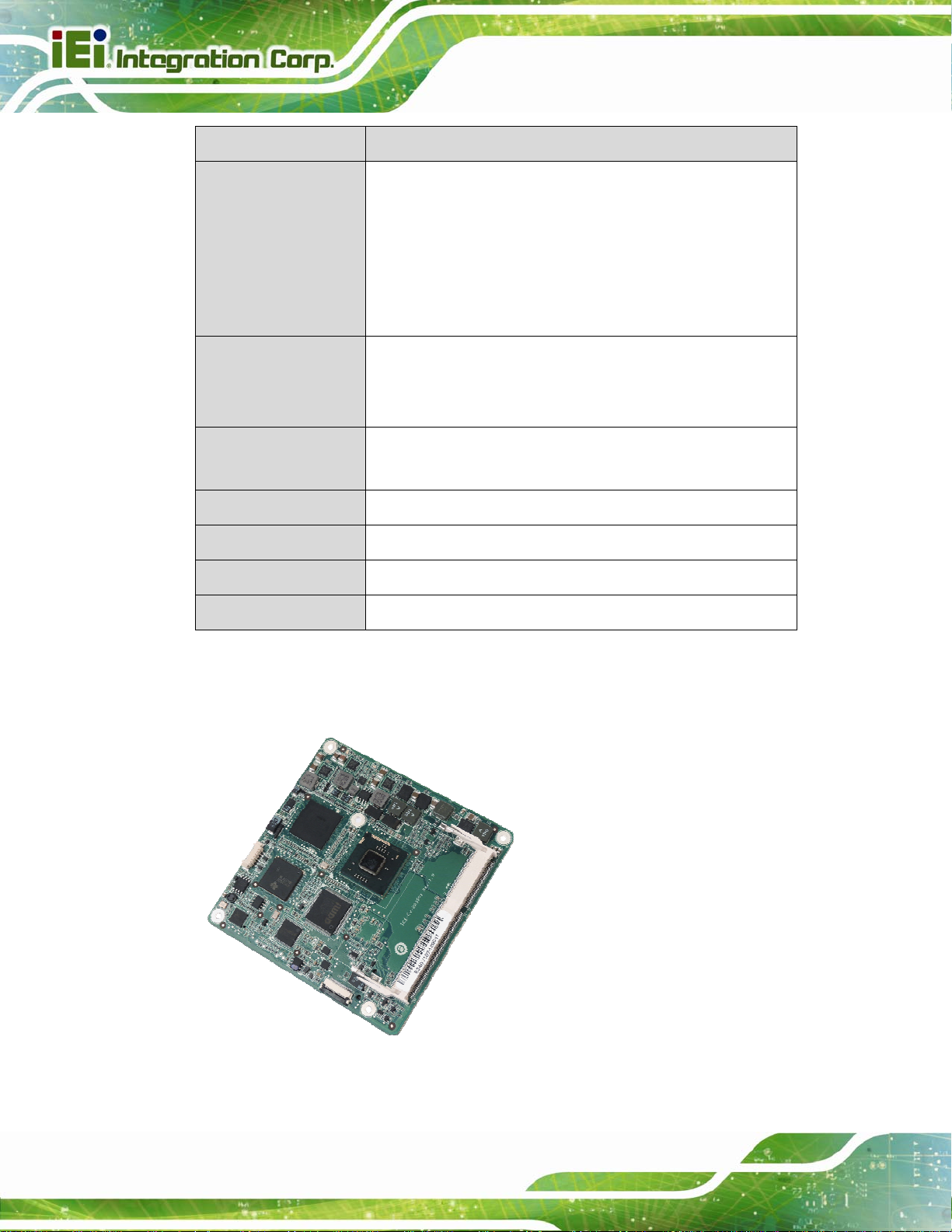
1.3 ICE-CV-D25501/N26001 COM Express Module
Figure 1-2: ICE-CV-D25501/N26001
Page 4
Page 15
Type 6 Carrier Board Design Guide
The ICE-CV-D25501/N26001 COM Express module provides the main processing chips
and is connected to a compatible COM Express baseboard. The ICE-CV-D25501/N26001
is equipped with an Intel® Atom™ D2550/N2600 CPU and Intel® NM10 PCH. The COM
Express standard allows the COM Express baseboard to be designed, while leaving the
choice of processor till the later stages of design. The ICE-CV-D25501/N26001 provides a
low power option with the full range of modern I/O options. The ICE-CV-D25501/N26001
embedded module is designed for flexible integration by system developers into
customized platform devices.
1.3.1 ICE-CV -D25501/N26001 Specifications
The ICE-CV-D25501/N26001 technical specifications are listed below.
Specifications/Model ICE-CV-D25501/N26001
Form Factor
CPU
Chipset
Memory
Graphics Engine
Display
(Signal to Baseboard)
PICMG COM Express R2.0 Type 6 for compact size (95 mm x 95 mm)
10 layers
1.86 GHz Intel® Atom™ D2550 dual-core CPU (2 x 512KB L2 cache)
1.6 GHz Intel® Atom™ N2600 dual-core CPU (2 x 512KB L2 cache)
Intel® NM10
D2550: One 1066 MHz DDR3/DDR3L (1.35V) SO-DIMM support (up to
4 GB)
N2600: One 800 MHz DDR3/DDR3L (1.35V) SO-DIMM support (up to
2 GB)
D2550: Intel® GMA 3650 with 640 MHz graphics core speed
N2600: Intel® GMA 3600 with 400 MHz graphics core speed
Supports DirectX 9 and Blu-ray 2.0
MPEG2, H.264, VC-1 and 1080p decoding
One VGA (up to 2048 x 1536 @ 75Hz) is integrated in the CPU
One LVDS is integrated in the CPU:
D2550: 24-bit single-channel LVDS (up to 1440 x 900 @ 60Hz)
N2600: 18-bit single-channel LVDS (up to 1366 x 768 @ 60Hz)
Ethernet
Two DDI (up to 2560 x 1600 @ 60Hz)
Realtek RTL8111E PCIe GbE controller
Page 5
Page 16
Specifications/Model ICE-CV-D25501/N26001
Type 6 Carrier Board Design Guide
BIOS
USB 3.0
Embedded Controller
Watchdog Timer
Expansion
I/O Interfaces
(Signal to Baseboard)
UEFI BIOS
ASMedia ASM1042
iWDD
Software programmable supports 1~255 sec. system reset
Four PCIe x1 (signal to baseboard)
Two USB 3.0
Eight USB 2.0
Two SATA 3Gb/s
Two UART (by EC)
HD Audio
GPIO
SMBus
I2C
LPC
SPI
Power Consumption
Operating
Temperature
Storage Temperature
Humidity (Operating)
Dimensions
Weight (GW/NW)
Table 1-2: ICE-CV-D25501/N26001 Specifications
+12V @ 0.45 A , Vcore_12V @ 1.0A (1.86 GHz Intel® Atom™ D2550
CPU with 2 GB 1066 MHz DDR3 SO-DIMM)
-10ºC ~ 60ºC
-20ºC ~ 70ºC
5% ~ 95% (non-condensing)
95 mm x 95 mm
600 g/200 g
Page 6
Page 17
Type 6 Carrier Board Design Guide
1.4 ICE-DB-T6 Reference Carrier Board
The ICE-DB-T6 is a full function carrier board for customers to apply or test the COM
Express Type 6 module. The carrier board can be used for any combination, including
software and hardware. Using the carrier board to develop and test the Type 6 module
also can achieve a quicker time to market. The ICE-DB-T6 is shown in
specifications are listed in
Table 1-3.
Figure 1-3 and the
Figure 1-3: ICE-DB-T6
1.4.1 ICE-DB-T6 Specifications
The ICE-DB-T6 technical specifications are listed below.
Specifications/Model ICE-DB-T6 Reference Carrier Board
Form Factor
CPU
Super I/O
ATX form factor baseboard
Support COM Express compact/basic module using Type 6
connector
Winbond W83627DHG
Page 7
Page 18
Specifications/Model ICE-DB-T6 Reference Carrier Board
Type 6 Carrier Board Design Guide
Audio
GPIO
Watchdog Timer
Display
Expansions
(Signal to Baseboard)
SMBus
I2C
Front Panel
Realtek ALC892 HD Audio codec
8-bit GPIO (GPIO from iWDD co-lay SDIO)
Software programmable supports1~255 sec. system reset
1 x 18/24-bit single/dual-channel LVDS
1 x VGA
3 x DisplayPort (two by external connector, one by pin header)
One PCIe x16
Five PCIe x1
Two PCIe Mini (with USB)
One LPC
One 4-pin wafer
One 4-pin wafer
One connector supports power LED, HDD LED, power button,
reset button, speaker/buzzer
TPM
Fan Connector
SD
Other Internal I/O
One 20-pin header
One 4-pin and one 3-pin CPU module fan connectors
One 3-pin system fan connector by SIO
One SD slot
4 x SATA 3Gb/s port
2 x RS-232 from COM Express (only TX, RX and GND)
2 x RS-232 from SIO
2 x USB 2.0
1 x Audio connector
Page 8
Page 19
Type 6 Carrier Board Design Guide
Specifications/Model ICE-DB-T6 Reference Carrier Board
1 x VGA
4 x USB 3.0
1 x RJ-45 GbE
External I/O
Power Supply
Operating
Temperature
Storage Temperature
Humidity (Operating)
Dimensions
Table 1-3: ICE-DB-T6 Specifications
2 x DisplayPort
3 x Audio jacks (Line-in, Line-out, Mic)
1 x PS/2 keyboard
1 x PS/2 mouse
ATX/AT p o w e r s upply
-10ºC ~ 60ºC
-20ºC ~ 70ºC
5% ~ 95% (non-condensing)
304.8 mm x 243.8 mm (12” x 9.6”)
Page 9
Page 20

Type 6 Carrier Board Design Guide
Chapter
2
2 Pin Assignments
Page 10
Page 21
Type 6 Carrier Board Design Guide
2.1 Chapter Overview
This chapter describes pin assignments and I/O characteristics for COM Express modules.
The carrier board uses two 220-pin 0.5 mm fine pitch board-to-board connectors. There
are seven different pin-out types currently defined by the COM Express Specification. The
preferred choice of the embedded computer industry is the Type 2 pin-out and the latest
pin-outs added in COM Express specification are Type 6 and Type 10. This design guide
focuses on the latest Type 6 pin-out which provides the latest technologies including PCI
Express, Serial ATA and DDI graphics.
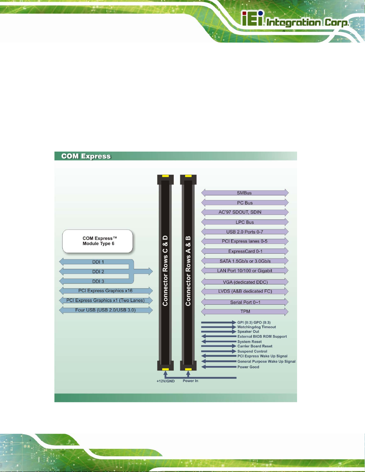
Figure 2-1: COM Express Type 6 Module Diagram
Page 11
Page 22
Type 6 Carrier Board Design Guide
2.2 COM Express Connector Type
The differences among the Module Types are summarized in Table 2-1.
Module Type 1 and 10 supports a single connector with two rows of pins
(220 pins total).
Module Types 2-6 support two connectors with four rows of pins
(440 pins total).
Type Rows PCIe
Lanes
1 AB Up to 6 - - - 4 1 8 / 0 VGA, LVDS
2 AB, CD Up to 22 1/2 32-bit 1 4 1 8 / 0 VGA, LVDS,
3 AB, CD Up to 22 1/2 32-bit - 4 3 8 / 0 VGA, LVDS,
4 AB, CD Up to 32 1/2 - 1 4 1 8 / 0 VGA, LVDS,
5 AB, CD Up to 32 1/2 - - 4 3 8 / 0 VGA, LVDS,
6 AB, CD Up to 24 1/NA - - 4 1 8 / 4 VGA, LVDS,
10 AB Up to 4 -/1 - - 2 1 8 / 0 1 x DDI
PEG/
SDVO
PCI IDE SATA LAN USB
2.0/3.0
Table 2-1: COM Express Connector Type Variations
Display
PEG/SDVO
PEG/SDVO
PEG/SDVO
PEG/SDVO
PEG, 3 x DDI
Page 12
Page 23
Type 6 Carrier Board Design Guide
2.3 Signal Table Terminology
The following section describes the signals found on the Type 6 connectors. Table 2-2
below describes the terminology used in this section for the Signal Description tables. The
“#” symbol at the end of the signal name indicates that the active or asserted state occurs
when the signal is at a low voltage level. When “#” is not present, the signal is asserted
when at a high voltage level.
Term Description
I/O Bi-directional signal
I Input signal
O Output signal
I/F Interface
GND Ground
PWR Power
OD Open drain output
PD Pull down
PU Pull up
+V12 +12V ±5% Volts Normal Power
+V5SB +5V ±5% Standby Power
+3.3VSB +3.3V ±5% Standby Power
+V3.3 +3.3V ±5% Volts Normal Power
+V5 +5V ±5% Volts Normal Power
# Active-Low Signals
‘+’ and ‘-‘ Differential Pairs
PM Power Management
GBE Gigabit Ethernet
Table 2-2: Conventions and Terminology
Page 13
Page 24
Type 6 Carrier Board Design Guide
2.4 Connector Pinout Row A and Row B
Pin Signal I/F I/O Pin Signal I/F I/O
A1 GND0 GND - B1 GND15 GND -
A2 GBE0_MDI3- GBE I/O B2 GBE0_ACT# GBE O 3.3V
A3 GBE0_MDI3+ GBE I/O B3 LPC_FRAME# LPC O 3.3V
A4 GBE0_LINK100# GBE O 3.3V B4 LPC_AD0 LPC I/O 3.3V
A5 GBE0_LINK1000# GBE O 3.3V B5 LPC_AD1 LPC I/O 3.3V
A6 GBE0_MDI2- GBE I/O B6 LPC_AD2 LPC I/O 3.3V
A7 GBE0_MDI2+ GBE I/O B7 LPC_AD3 LPC I/O 3.3V
A8 GBE0_LINK# GBE O 3.3V B8 LPC_DRQ0# LPC I 3.3V
A9 GBE0_MDI1- GBE I/O B9 LPC_DRQ1# LPC I 3.3V
A10 GBE0_MDI1+ GBE I/O B10 LPC_CLK LPC O 3.3V
A11 GND1 GND - B11 GND16 GND -
A12 GBE0_MDI0- GBE I/O B12 PWRBTN# PM I
A13 GBE0_MDI0+ GBE I/O B13 SMB_CK SMB -
A14 GBE0_CTREF GBE B14 SMB_DAT SMB -
A15 SUS_S3# PM O B15 SMB_ALERT# SMB I
A16 SATA0_TX+ SATA O B16 SATA1_TX+ SATA O
A17 SATA0_TX- SATA O B17 SATA1_TX- SATA O
A18 SUS_S4# PM O B18 SUS_STAT# PM O
A19 SATA0_RX+ SATA I B19 SATA1_RX+ SATA I
A20 SATA0_RX- SATA I B20 SATA1_RX- SATA I
A21 GND2 GND - B21 GND17 GND -
A22 SATA2_TX+ SATA O B22 SATA3_TX+ SATA O
A23 SATA2_TX- SATA O B23 SATA3_TX- SATA O
A24 SUS_S5# PM O B24 PWR_OK PM I
A25 SATA2_RX+ SATA I B25 SATA3_RX+ SATA I
A26 SATA2_RX- SATA I B26 SATA3_RX- SATA I
A27 BATLOW# PM I B27 WDT - -
A28 ATA_ACT# SATA O 3.3V B28 AC/HD_SDIN2 HDA I 3.3V
A29 AC/HD _SYNC HDA O 3.3V B29 AC/HD_SDIN1 HDA I 3.3V
A30 AC/HD _RST# HDA O 3.3V B30 AC/HD_SDIN0 HDA I 3.3V
A31 GND3 GND - B31 GND18 GND -
A32 AC/HD_BITCLK HDA O 3.3V B32 SPKR - -
A33 AC/HD_SDOUT HDA O 3.3V B33 I2C_CK I2C -
A34 BIOS_DISABLE# - - B34 I2C_DAT I2C -
A35 THRMTRIP# PM O B35 THRM# PM I
A36 USB6- USB I/O B36 USB7- USB I/O
A37 USB6+ USB I/O B37 USB7+ USB I/O
A38 USB_6_7_OC# USB I 3.3V B38 USB_4_5_OC# USB I 3.3V
A39 USB4- USB I/O B39 USB5- USB I/O
A40 USB4+ USB I/O B40 USB5+ USB I/O
A41 GND4 GND - B41 GND19 GND -
A42 USB2- USB I/O B42 USB3- USB I/O
A43 USB2+ USB I/O B43 USB3+ USB I/O
A44 USB_2_3_OC# USB I 3.3V B44 USB_0_1_OC# USB I 3.3V
A45 USB0- USB I/O B45 USB1- USB I/O
Page 14
Page 25
Type 6 Carrier Board Design Guide
Pin Signal I/F I/O Pin Signal I/F I/O
A46 USB0+ USB I/O B46 USB1+ USB I/O
A47 VCC_RTC PWR -- B47 EXCD1_PERST# PCIE -
A48 EXCD0_PERST# PCIE - B48 EXCD1_CPPE# PCIE -
A49 EXCD0_CPPE# PCIE - B49 SYS_RESET# PM I
A50 LPC_SERIRQ LPC I/O
3.3V
A51 GND5 GND - B51 GND20 GND -
A52 PCIE_TX5+ PCIE O B52 PCIE_RX5+ PCIE I
A53 PCIE_TX5- PCIE O B53 PCIE_RX5- PCIE I
A54 GPI0 GPIO I B54 GPO1 GPIO O
A55 PCIE_TX4+ PCIE O B55 PCIE_RX4+ PCIE I
A56 PCIE_TX4- PCIE O B56 PCIE_RX4- PCIE I
A57 GND6 GND - B57 GPO2 GPIO O
A58 PCIE_TX3+ PCIE O B58 PCIE_RX3+ PCIE I
A59 PCIE_TX3- PCIE O B59 PCIE_RX3- PCIE I
A60 GND7 GND - B60 GND21 GND -
A61 PCIE_TX2+ PCIE O B61 PCIE_RX2+ PCIE I
A62 PCIE_TX2- PCIE O B62 PCIE_RX2- PCIE I
A63 GPI1 GPIO I B63 GPO3 GPIO O
A64 PCIE_TX1+ PCIE O B64 PCIE_RX1+ PCIE I
A65 PCIE_TX1- PCIE O B65 PCIE_RX1- PCIE I
A66 GND8 GND - B66 WAKE0# PCIE I
A67 GPI2 GPIO I B67 WAKE1# PM I
A68 PCIE_TX0+ PCIE O B68 PCIE_RX0+ PCIE I
A69 PCIE_TX0- PCIE O B69 PCIE_RX0- PCIE I
A70 GND9 GND - B70 GND22 GND -
A71 LVD S_A0+ LVD S O B71 LVDS_B0+ LVDS O
A72 LVD S_A0- LVDS O B72 LVDS_B0 - LV D S O
A73 LVD S_A1+ LVD S O B73 LVDS_B1+ LVDS O
A74 LVD S_A1- LVDS O B74 LVDS_B1 - LV D S O
A75 LVD S_A2+ LVD S O B75 LVDS_B2+ LVDS O
A76 LVD S_A2- LVDS O B76 LVDS_B2 - LV D S O
A77 LVDS_VDD_EN LVDS O 3.3V B77 LVDS_B3+ LVDS O
A78 LVD S_A3+ LVD S O B78 LVDS_B3- LVDS O
A79 LVD S_A3- LVDS O B79 LVDS_BKLT_EN LVDS O 3.3V
A80 GND GND - B80 GND GND -
A81 LVD S_A_CK+ LVDS O B81 LV D S _ B _ C K+ LVDS O
A82 LVD S_A_CK- LVDS O B82 LVDS_B_ C K - LV D S O
A83 LVDS_I2C_CK LVDS O 3.3V B83 LVDS_BKLT_CTRL LVDS O 3.3V
A84 LVDS_I2C_DAT LVDS IO 3.3V B84 VCC5SBY1 PWR -
A85 GPI3 GPIO I B85 VCC5SBY2 PWR -
A86 RSVD - - B86 VCC5SBY3 PWR -
A87 RSVD - - B87 VCC5SBY4 PWR -
A88 PCIE0_CK_REF+ PCIE O B88 BIOS_DIS1# - I 3.3V
A89 PCIE0_CK_REF- PCIE O B89 VGA_RED VGA O
A90 GND11 GND - B90 GND 24 GND -
A91 SPI_VCC SPI O 3.3V B91 VGA_GRN VGA O
A92 SPI_MISO SPI IO 3.3V B92 VGA_BLU VGA O
B50 CB_RESET# PM O
Page 15
Page 26
Pin Signal I/F I/O Pin Signal I/F I/O
A93 GPO0 GPIO O B93 VGA_HSYNC VGA O
A94 SPI_CLK SPI O B94 VGA_VSYNC VGA O
A95 SPI_MOSI SPI IO B95 VGA_I2C_CK VGA I/O
A96 PP_TPM TPM I B96 VGA_I2C_DAT VGA I/O
A97 RSVD - - B97 SPI_CS# SPI O
A98 RS1_TX UART O B98 RSVD - -
A99 RS1_RX UART I B99 RSVD - -
A100 GND13 GND - B100 GND25 GND -
A101 RS2_TX UART O B101 FAN_PWMOUT FAN O
A102 RS2_RX UART I B102 FAN_TACHIN FAN I
A103 LID# - I B103 SLEEP# - I
A104 VCC_12V7 PWR - B104 VCC_12V16 PWR -
A105 VCC_12V8 PWR - B105 VCC_12V17 PWR -
A106 VCC_12V9 PWR - B106 VCC_12V18 PWR -
A107 VCC_12V10 PWR - B107 VCC_12V19 PWR -
A108 VCC_12V11 PWR - B108 VCC_12V20 PWR -
A109 VCC_12V12 PWR - B109 VCC_12V21 PWR -
A110 GND14 GND - B110 GND26 GND -
Type 6 Carrier Board Design Guide
2.5 Connector Pinout Rows C and D
Pin Signal I/F I/O Pin Signal I/F I/O
C1 GND0 GND - D1 GND15 GND -
C2 GND GND - D2 GND GND -
C3 USB_SSRX0- USB 3.0 I D3 USB_SSTX0- USB 3.0 O
C4 USB_SSRX0+ USB 3.0 I D4 USB_SSTX0+ USB 3.0 O
C5 GND GND - D5 GND GND -
C6 USB_SSRX1- USB 3.0 I D6 USB_SSTX1- USB 3.0 O
C7 USB_SSRX1+ USB 3.0 I D7 USB_SSTX1+ USB 3.0 O
C8 GND GND - D8 GND GND -
C9 USB_SSRX2- USB 3.0 I D9 USB_SSTX2- USB 3.0 O
C10 USB_SSRX2+ USB 3.0 I D10 USB_SSTX2+ USB 3.0 O
C11 GND1 GND - D11 GND16 GND -
C12 USB_SSRX3- USB 3.0 I D12 USB_SSTX3- USB 3.0 O
C13 USB_SSRX3+ USB 3.0 I D13 USB_SSTX3+ USB 3.0 O
C14 GND GND - D14 GND GND -
C15 DDI1_PAIR6+ DDI O D15 DDI1_AUX+ DDI O
C16 DDI1_PAIR6- DDI O D16 DDI1_AUX- DDI O
C17 RSVD - - D17 RSVD - -
C18 RSVD - - D18 RSVD - -
C19 PCIE_RX6+ PCIE I D19 PCIE_TX6+ PCIE O
C20 PCIE_RX6- PCIE I D20 PCIE_TX6- PCIE O
C21 GND2 GND - D21 GND17 GND -
C22 RSVD - - D22 RSVD - -
C23 RSVD - - D23 RSVD - -
C24 DDI1_HPD DDI I D24 RSVD - -
C25 DDI1_PAIR4+ DDI O D25 RSVD - -
Page 16
Page 27
Type 6 Carrier Board Design Guide
Pin Signal I/F I/O Pin Signal I/F I/O
C26 DDI1_PAIR4- DDI O D26 DDI1_PAIR0+ DDI O
C27 RSVD - - D27 DDI1_PAIR0- DDI O
C28 RSVD - - D28 RSVD - -
C29 DDI1_PAIR5+ DDI O D29 DDI1_PAIR1+ DDI O
C30 DDI1_PAIR5- DDI O D30 DDI1_PAIR1- DDI O
C31 GND3 GND - D31 GND18 GND -
C32 DDI2_AUX+ DDI O D32 DDI1_PAIR2+ DDI O
C33 DDI2_AUX- DDI O D33 DDI1_PAIR2- DDI O
C34 DDI2_CTRLCLK DDI O D34 DDI2_CTRLDATA DDI O
C35 RSVD - - D35 RSVD - -
C36 DDI3_AUX+ DDI O D36 DDI1_PAIR3+ DDI O
C37 DDI3_AUX- DDI O D37 DDI1_PAIR3- DDI O
C38 DDI3_CTRLCLK DDI O D38 DDI3_CTRLDATA DDI O
C39 DDI3_PAIR0+ DDI O D39 DDI2_PAIR0+ DDI O
C40 DDI3_PAIR0- DDI O D40 DDI2_PAIR0- DDI O
C41 GND4 GND - D41 GND19 GND -
C42 DDI3_PAIR1+ DDI O D42 DDI2_PAIR1+ DDI O
C43 DDI3_PAIR1- DDI O D43 DDI2_PAIR1- DDI O
C44 DDI3_HPD DDI I D44 DDI2_HPD DDI I
C45 RSVD - - D45 RSVD - -
C46 DDI3_PAIR2+ DDI O D46 DDI2_PAIR2+ DDI O
C47 DDI3_PAIR2- DDI O D47 DDI2_PAIR2- DDI O
C48 RSVD - - D48 RSVD - -
C49 DDI3_PAIR3+ DDI O D49 DDI2_PAIR3+ DDI O
C50 DDI3_PAIR3- DDI O D50 DDI2_PAIR3- DDI O
C51 GND5 GND - D51 GND20 GND -
C52 PEG_RX0+ PEG I D52 PEG_TX0+ PEG O
C53 PEG_RX0- PEG I D53 PEG_TX0- PEG O
C54 RSVD - - D54 PEG_LANE_RV#
C55 PEG_RX1+ PEG I D55 PEG_TX1+ PEG O
C56 PEG_RX1- PEG I D56 PEG_TX1- PEG O
C57 RSVD - - D57 TYPE2#
C58 PEG_RX2+ PEG I D58 PEG_TX2+ PEG O
C59 PEG_RX2- PEG I D59 PEG_TX2- PEG O
C60 GND7 GND - D60 GND21 GND -
C61 PEG_RX3+ PEG I D61 PEG_TX3+ PEG O
C62 PEG_RX3- PEG I D62 PEG_TX3- PEG O
C63 RSVD1 - - D63 RSVD9 - -
C64 RSVD2 - - D64 RSVD10 - -
C65 PEG_RX4+ PEG I D65 PEG_TX4+ PEG O
C66 PEG_RX4- PEG I D66 PEG_TX4- PEG O
C67 RSVD3 - O D67 GND28 GND -
C68 PEG_RX5+ PEG I D68 PEG_TX5+ PEG O
C69 PEG_RX5- PEG I D69 PEG_TX5- PEG O
C70 GND9 GND - D70 GND22 GND -
C71 PEG_RX6+ PEG I D71 PEG_TX6+ PEG O
C72 PEG_RX6- PEG I D72 PEG_TX6- PEG O
C73 DDI1_CTRLDATA DDI O D73 DDI1_CTRLCLK DDI O
Page 17
Page 28
Pin Signal I/F I/O Pin Signal I/F I/O
C74 PEG_RX7+ PEG I D74 PEG_TX7+ PEG O
C75 PEG_RX7- PEG I D75 PEG_TX7- PEG O
C76 GND8 GND - D76 GND29 GND -
C77 RSVD4 - - D77 RSVD - -
C78 PEG_RX8+ PEG I D78 PEG_TX8+ PEG O
C79 PEG_RX8- PEG I D79 PEG_TX8- PEG O
C80 GND10 GND - D80 GND23 GND -
C81 PEG_RX9+ PEG I D81 PEG_TX9+ PEG O
C82 PEG_RX9- PEG I D82 PEG_TX9- PEG O
C83 RSVD5 - - D83 RSVD8 - -
C84 GND6 GND - D84 GND30 GND -
C85 PEG_RX10+ PEG I D85 PEG_TX10+ PEG O
C86 PEG_RX10- PEG I D86 PEG_TX10- PEG O
C87 GND35 GND - D87 GND31 GND -
C88 PEG_RX11+ PEG I D88 PEG_TX11+ PEG O
C89 PEG_RX11- PEG I D89 PEG_TX11- PEG O
C90 GND27 GND - D90 GND24 GND -
C91 PEG_RX12+ PEG I D91 PEG_TX12+ PEG O
C92 PEG_RX12- PEG I D92 PEG_TX12- PEG O
C93 GND11 GND - D93 GND32 GND -
C94 PEG_RX13+ PEG I D94 PEG_TX13+ PEG O
C95 PEG_RX13- PEG I D95 PEG_TX13- PEG O
C96 GND12 GND - D96 GND33 GND -
C97 RSVD6 - - D97 PEG_ENABLE# PEG I
C98 PEG_RX14+ PEG I D98 PEG_TX14+ PEG O
C99 PEG_RX14- PEG I D99 PEG_TX14- PEG O
C100 GND13 GND - D100 GND25 GND -
C101 PEG_RX15+ PEG I D101 PEG_TX15+ PEG O
C102 PEG_RX15- PEG I D102 PEG_TX15- PEG O
C103 GND GND - D103 GND34 GND -
C104 VCC_12V1 PWR - D104 VCC_12V7 PWR -
C105 VCC_12V2 PWR - D105 VCC_12V8 PWR -
C106 VCC_12V3 PWR - D106 VCC_12V9 PWR -
C107 VCC_12V4 PWR - D107 VCC_12V10 PWR -
C108 VCC_12V5 PWR - D108 VCC_12V11 PWR -
C109 VCC_12V6 PWR - D109 VCC_12V12 PWR -
C110 GND14 GND - D110 GND26 GND -
Type 6 Carrier Board Design Guide
Page 18
Page 29
Type 6 Carrier Board Design Guide
Chapter
3
3 Signal Description and
Routing Guideline
Page 19
Page 30
Type 6 Carrier Board Design Guide
3.1 PEG (PCI Express Graphic)
The PEG Port can utilize COM Express PCIe lanes 16 through 32 to drive a PCIe x16 link
for a PCI Express Graphics card. It supports a theoretical bandwidth of up to 4 GB/s. Each
lane of the PEG Port consists of a receiver and transmit differential signal pair. The
corresponding signals can be found on the Module connector rows C and D.
3.1.1 Signal Description
Pin Signal I/O Description
C52
C53
D52
D53
C55
C56
D55
D56
C58
C59
D58
D59
C61
C62
D61
D62
C65
C66
D65
D66
C68
C69
D68
D69
C71
C72
D71
D72
C74
C75
D74
D75
C78
C79
D78
D79
C81
C82
PEG_RX0+
PEG_RX0PEG_TX0+
PEG_TX0PEG_RX1+
PEG_RX1PEG_TX1+
PEG_TX1PEG_RX2+
PEG_RX2PEG_TX2+
PEG_TX2PEG_RX3+
PEG_RX3PEG_TX3+
PEG_TX3PEG_RX4+
PEG_RX4PEG_TX4+
PEG_TX4PEG_RX5+
PEG_RX5PEG_TX5+
PEG_TX5PEG_RX6+
PEG_RX6PEG_TX6+
PEG_TX6PEG_RX7+
PEG_RX7PEG_TX7+
PEG_TX7PEG_RX8+
PEG_RX8PEG_TX8+
PEG_TX8PEG_RX9+
PEG_RX9-
I PEG Port 0. Receive Input differential pair.
O PEG Port 0. Transmit Output differential pair.
I PEG Port 1. Receive Input differential pair.
O PEG Port 1. Transmit Output differential pair.
I PEG Port 2. Receive Input differential pair.
O PEG Port 2. Transmit Output differential pair.
I PEG Port 3. Receive Input differential pair.
O PEG Port 3. Transmit Output differential pair.
I PEG Port 4. Receive Input differential pair.
O PEG Port 4. Transmit Output differential pair.
I PEG Port 5. Receive Input differential pair.
O PEG Port 5. Transmit Output differential pair.
I PEG Port 6. Receive Input differential pair.
O PEG Port 6. Transmit Output differential pair.
I PEG Port 7. Receive Input differential pair.
O PEG Port 7. Transmit Output differential pair.
I PEG Port 8,. Receive Input differential pair.
O PEG Port 8. Transmit Output differential pair.
I PEG Port 9,. Receive Input differential pair.
Page 20
Page 31

Type 6 Carrier Board Design Guide
D81
D82
C85
C86
D85
D86
C88
C89
D88
D89
C91
C92
D91
D92
C94
C95
D94
D95
C98
C99
D98
D99
C101
C102
D101
D102
A88
A89
D54 PEG_LANE_RV# I 3.3V
D97 PEG_ENABLE# I 3.3V
PEG_TX9+
PEG_TX9PEG_RX10+
PEG_RX10PEG_TX10+
PEG_TX10PEG_RX11+
PEG_RX11PEG_TX11+
PEG_TX11PEG_RX12+
PEG_RX12PEG_TX12+
PEG_TX12PEG_RX13+
PEG_RX13PEG_TX13+
PEG_TX13PEG_RX14+
PEG_RX14PEG_TX14+
PEG_TX14PEG_RX15+
PEG_RX15PEG_TX15+
PEG_TX15PCIE_CLK_REF
+
PCIE_CLK_REF-
O PEG Port 9. Transmit Output differential pair.
I PEG Port 10.. Receive Input differential pair.
O PEG Port 10.Transmit Output differential pair.
I PEG Port 11. Receive Input differential pair.
O PEG Port 11. Transmit Output differential pair.
I PEG Port 12. Receive Input differential pair.
O PEG Port 12. Transmit Output differential pair.
I PEG Port 13,. Receive Input differential pair.
O PEG Port 13. Transmit Output differential pair.
I PEG Port 14.. Receive Input differential pair.
O PEG Port 14. Transmit Output differential pair.
I PEG Port 15. Receive Input differential pair.
O PEG Port 15. Transmit Output differential pair.
O PCIe Reference Clock for all COM Express
CMOS
CMOS
PCIe lanes, and for PEG lanes
PCI Express Graphics lane reversal input strap.
Pull low on the carrier board to reverse lane
order.
PEG enable function. Strap to enable PCI
Express x16 external graphics interface. Pull low
to disable internal graphics and enable the x16
interface.
PS: IEI BIOS auto detects the SDVO or
PCIe x16, please reserve for future use
Table 3-1: PCI Express Signal Descriptions
Page 21
Page 32

3.1.2 PEG Connector
Figure 3-1 illustrates the pinout definition for the standard PCI Express x16 connectors.
Type 6 Carrier Board Design Guide
+V3.3_DUAL
SMB_CK3,4, 5,10,11,1 7,20
SMB_DAT3,4,5, 10,11,17, 20
PCIE_WAKE_U P#3,5, 10,16
PEG_TX0+3
PEG_TX0-3
SDVO_I2C_CK3
PEG_TX1+3
PEG_TX1-3
PEG_TX2+3
PEG_TX2-3
PEG_TX3+3
PEG_TX3-3
SDVO_I2C_D AT3
PEG_TX4+3
PEG_TX4-3
PEG_TX5+3
PEG_TX5-3
PEG_TX6+3
PEG_TX6-3
PEG_TX7+3
PEG_TX7-3
PEG_TX8+3
PEG_TX8-3
PEG_TX9+3
PEG_TX9-3
PEG_TX10+3
PEG_TX10-3
PEG_TX11+3
PEG_TX11-3
PEG_TX12+3
PEG_TX12-3
PEG_TX13+3
PEG_TX13-3
PEG_TX14+3
PEG_TX14-3
PEG_TX15+3
PEG_TX15-3
+V12 +V3.3
PCIEX16_1
TP43
B10
B11
B12
B13
B14
B15
B16
B17
B18
B19
B20
B21
B22
B23
B24
B25
B26
B27
B28
B29
B30
B31
B32
B33
B34
B35
B36
B37
B38
B39
B40
B41
B42
B43
B44
B45
B46
B47
B48
B49
B50
B51
B52
B53
B54
B55
B56
B57
B58
B59
B60
B61
B62
B63
B64
B65
B66
B67
B68
B69
B70
B71
B72
B73
B74
B75
B76
B77
B78
B79
B80
B81
B82
B1
B2
B3
B4
B5
B6
B7
B8
B9
+12V03
+12V04
RSVD05
GND35
SMBCLK
SMBDATA
GND36
3_3V03
JTAG1
3_3VAUX
WAKE#
RSVD06
GND37
HSOP0
HSON0
GND38
PRSNT2#01
GND39
HSOP1
HSON1
GND40
GND41
HSOP2
HSON2
GND42
GND43
HSOP3
HSON3
GND44
RSVD07
PRSNT2#02
GND45
HSOP4
HSON4
GND46
GND47
HSOP5
HSON5
GND48
GND49
HSOP6
HSON6
GND50
GND51
HSOP7
HSON7
GND52
PRSNT2#03
GND53
HSOP8
HSON8
GND54
GND55
HSOP9
HSON9
GND56
GND57
HSOP10
HSON10
GND58
GND59
HSOP11
HSON11
GND60
GND61
HSOP12
HSON12
GND62
GND63
HSOP13
HSON13
GND64
GND65
HSOP14
HSON14
GND66
GND67
HSOP15
HSON15
GND68
PRSNT2#04
RSVD08
NC1
PCIE_X16
NC2
NC1
NC2
PRSNT1#
+12V01
+12V02
GND01
JTAG2
JTAG3
JTAG4
JTAG5
3_3V01
3_3V02
PWRGD
GND02
REFCLK+
REFCLK-
GND03
HSIP0
HSIN0
GND04
RSVD01
GND05
HSIP1
HSIN1
GND06
GND07
HSIP2
HSIN2
GND08
GND09
HSIP3
HSIN3
GND10
RSVD02
RSVD03
GND11
HSIP4
HSIN4
GND12
GND13
HSIP5
HSIN5
GND14
GND15
HSIP6
HSIN6
GND16
GND17
HSIP7
HSIN7
GND18
RSVD04
GND19
HSIP8
HSIN8
GND20
GND21
HSIP9
HSIN9
GND22
GND23
HSIP10
HSIN10
GND24
GND25
HSIP11
HSIN11
GND26
GND27
HSIP12
HSIN12
GND28
GND29
HSIP13
HSIN13
GND30
GND31
HSIP14
HSIN14
GND32
GND33
HSIP15
HSIN15
GND34
A1
A2
A3
A4
A5
A6
A7
A8
A9
A10
A11
A12
A13
A14
A15
A16
A17
A18
A19
A20
A21
A22
A23
A24
A25
A26
A27
A28
A29
A30
A31
A32
A33
A34
A35
A36
A37
A38
A39
A40
A41
A42
A43
A44
A45
A46
A47
A48
A49
A50
A51
A52
A53
A54
A55
A56
A57
A58
A59
A60
A61
A62
A63
A64
A65
A66
A67
A68
A69
A70
A71
A72
A73
A74
A75
A76
A77
A78
A79
A80
A81
A82
+V12+V3.3
CB_RESET# 3,5, 10,11,14,20
CLK100M_PCIEx16_SLOT+ 4
R1710_4 12
R2230_4 12
R2240_4 12
R2250_4 12
R2260_4 12
R2270_4 12
R2280_4 12
R3760_4 12
R3780_4 12
R3790_4 12
R3800_4 12
R3810_4 12
R3820_4 12
R3830_4 12
R3840_4 12
R3850_4 12
R3860_4 12
R3870_4 12
R3880_4 12
R3890_4 12
R3900_4 12
R3910_4 12
R3920_4 12
R3930_4 12
R3940_4 12
R3950_4 12
R3960_4 12
R3970_4 12
R3990_4 12
R4000_4 12
R4010_4 12
CLK100M_PCIEx16_SLOT- 4
PEG_RX0+ 3
PEG_RX0- 3
PEG_RX1+ 3
PEG_RX1- 3
PEG_RX2+ 3
PEG_RX2- 3
PEG_RX3+ 3
PEG_RX3- 3
PEG_RX4+ 3
PEG_RX4- 3
PEG_RX5+ 3
PEG_RX5- 3
PEG_RX6+ 3
PEG_RX6- 3
PEG_RX7+ 3
PEG_RX7- 3
PEG_RX8+ 3
PEG_RX8- 3
PEG_RX9+ 3
PEG_RX9- 3
PEG_RX10+ 3
PEG_RX10- 3
PEG_RX11+ 3
PEG_RX11- 3
PEG_RX12+ 3
PEG_RX12- 3
PEG_RX13+ 3
PEG_RX13- 3
PEG_RX14+ 3
PEG_RX14- 3
PEG_RX15+ 3
PEG_RX15- 3
1
TP61
1
TP62
1
TP63
1
TP68
1
TP71
1R3770_4 12
TP72
1
TP73
1
TP74
1
TP75
1
TP76
1
TP77
1
TP78
1
TP79
1
TP81
1
TP82
1
TP83
1
TP84
1
TP85
1
TP86
1
TP87
Figure 3-1: PCI Express x16 Slot Example
Page 22
Page 33

Type 6 Carrier Board Design Guide
3.1.3 PEG_ENABLE#
PEG_ENABLE# is defined on the COM Express connector as a method to configure the
COM Express PCIe lanes 16 through 32 on the C-D connector as a PCI Express Graphics
port for an external graphics device. The usual effect of pulling PEG_ENABLE# low is to
disable the on-Module graphics engine. For some modules, it is possible to configure the
module such that the internal graphics engine remains active, even when the external
PEG interface is being used for a Carrier Board graphics device. This is Module
dependent. ICE Modules implement the auto-detect function. So, please reserve this pin
for future use.
3.1.4 PCI Express Test Points and Probing
IEI follows the suggestion provided by Intel® to preserve 0-Ω on the carrier board. The
inclusion of test points and probing structures has the ability to impact the loss and jitter
budgets of a PCI Express interconnect. This is not to say that they cannot be tolerated. In
general, test points and probe structures should not introduce stubs on the differential
pairs or cause significant deviation from the recommendations given throughout this
chapter. Existing vias, pads or pins should be used wherever possible to accommodate
such structures. Careful consideration must be taken whenever additional probing
structures are used.
The PCI Express based specification requires the data eyes to be measured into a 50-Ω
resistor terminated to ground. To facilitate the measurement, an additional test structure
may be required on a test board. This test structure should not be included in a production
board because it will affect the overall signal quality and resulting margins. The three-pad
test structure consists of the footprints of two resistors, perpendicular to each other
forming a “L” shape. The resistor package/footprint should be as small as possible,
preferably 0402. To enable the test mode, a 50 Ω ±1% resistor stuffing option is needed to
break the path. This will force the transmitter port to enter the compliance mode and begin
transmitting the compliance packet. Otherwise, use a 0-Ω resistor to continue the trace
route to the Rx port. This will allow normal operation of the device.
Page 23
Page 34

Type 6 Carrier Board Design Guide
Figure 3-2: Intel Recommend Test Structure for PCI Express Data Eye Measurement
3.1.5 PCI Express Routing Guideline
3.1.5.1 Impedance Consideration
The PCI Express impedance considerations are listed in Table 3-2.
Table 3-2: PCI Express Impedance Consideration
Parameters Routing
Transfer Rate / PCIe Lane 2.5 Gbits/sec
Maximum signal line length (coupled traces) TX and RX path: 21.0 inches
Maximum signal length allowance on the
COM Express module "
Signal length allowance on the COM
Express carrier board "
Differential Impedance 100 Ohms +/-20%
Single-ended Impedance 55 Ohms +/-15%
Trace width (W) 5 mils (microstrip routing) (*)
Spacing between differential pairs (intra-pair)
(S)
Spacing between RX and TX pairs
(inter-pair) (s)
Spacing between differential pairs and
high-speed periodic signals
Spacing between differential pairs and
low-speed non periodic signals
Length matching between differential pairs
(intra-pair)
TX and RX path: 5.15 inches
TX and RX path: 15.85 inches @
0.28dB/GHz/inch to PCIe device 9.00 inches
@ 0.28dB/GHz/inch to PCIe slot
4 mils (microstrip routing) (*)
Min. 20mils
Min. 50mils
Min. 20mils
Max. 5mils
Page 24
Page 35

Type 6 Carrier Board Design Guide
Length matching between RX and TX pairs
(inter-pair)
Length matching between reference clock
differential pairs REFCLK+ and REFCLK(intra-pair)
Length matching between reference clock
pairs (inter-pair)
Reference plain GND referenced preferred
Spacing from edge of plane Min. 40mils
Via Usage
AC coupling capacitors
No strict electrical requirements. Keep
difference within a 3.0 inch delta to minimize
latency.
Max. 5mils
No electrical requirements.
Max. 2 vias per TX trace Max. 4 vias per RX
trace
The AC coupling capacitors for the TX lines
are incorporated on the COM Express
module. The AC coupling capacitors for RX
signal lines have to be implemented on the
customer COM Express" carrier board.
Capacitor type: X7R
3.1.5.2 AC Coupling Capacitors
TX AC coupling capacitor is already embedded in the ICE modules. Users only need to
add the RX AC coupling capacitor on the carrier board. The PCI Express specification
requires that each lane of a PCI Express link be AC coupled between the driver and
receiver. The specification allows for the AC coupling capacitors to be located either on or
off the die. However, the AC coupling will be separated from the die and in the form of
discrete capacitors on the motherboard itself in most cases. The 0603 size capacitors are
acceptable, but the smaller size 0402 capacitors are strongly encouraged for reducing the
overall board area needed to place the capacitors.
Page 25
Page 36

Type 6 Carrier Board Design Guide
ICE Module
AC Coupling Cap
Figure 3-3: PEG Lane Connection Topology Example
3.1.5.3 Routing Notices
Each signal and its complement in a differential pair should be length
PEG SLOT or SDVO Device
TX+
TX-
RX+
RX-
matched whenever possible on a segment-by-segment basis at the point of
discontinuity. Examples of segments might include breakout areas, routes to
connect vias, routes to connect an AC coupling capacitor, routes to connect a
connector, and so forth.
When trace length matching occurs, it should be made as close as possible to
the point where the length variation occurs, as shown in
example, length matching in a chipset breakout area or connector pin field
should occur within the first 125 mils (3.175 mm) of the structure that causes
the length mismatch.
When serpentining is needed to match lengths, the trace spacing should not
become greater than two times the original spacing. The length of the
increased spacing should not be greater than three times the trace width. See
Figure 3-4. In determining the overall length of a given signal in a differential
pair, use pad or pin edge-to-edge distances rather than the total etch present,
unless the amount of trace routing inside each pad is identical. The amount of
etch within a given pad is electrically part of the pad itself. In other words, only
the etch outside of the pad edge is relevant to the overall length of a
Figure 3-4. For
Page 26
differential pair.
Page 37

Type 6 Carrier Board Design Guide
Preferred Routing
Bad Routing
Alternative Routing
Preferred Routing
Figure 3-4: PEG Layout Trace Example
3.2 PCI Express
PCI Express provides a scalable, high-speed, serial I/O point-to-point bus connection. A
PCI Express lane consists of dual simplex channels, each implemented as a low-voltage
differentially driven transmit pair and receive pair. They are used for simultaneous
Preferred Routing
transmission in each direction. The bandwidth of a PCI Express link can be scaled by
adding signal pairs to form multiple lanes between two devices. The PCI Express
specification defines x1, x4, x8, x16, and x32 link widths. Each single lane has a raw data
transfer rate of 2.5Gbps @ 1.25GHz.
Page 27
Page 38
The PCI Express interface of the COM Express module consists of up to six lanes, each
with a receive and transmit differential signal pair. According to the PCI Express
specification, these six lanes can be configured as several PCI Express x1 links or to a
combined x4 link plus two x1 links. These configuration possibilities are based on the
COM Express module's chipset capabilities.
3.2.1 Signal Description
Pin Signal I/O Description
Type 6 Carrier Board Design Guide
B68
B69
A68
A69
B64
B65
A64
A65
B61
B62
A61
A62
B58
B59
A58
A59
B55
B56
A55
A56
B52
B53
A52
A53
A88
A89
B66 WAKE0# I PCIE PCIe Wake Event: Sideband wake-up signal.
A49 EXCD0_CPPE# I 3.3V
B48 EXCD1_CPPE# I 3.3V
A48 EXCD0_PERST# O 3.3V
B47 EXCD1_PERST# O 3.3V
PCIE_RX0+
PCIE_RX0PCIE_TX0+
PCIE_TX0PCIE_RX1+
PCIE_RX1PCIE_TX1+
PCIE_TX1PCIE_RX2+
PCIE_RX2PCIE_TX2+
PCIE_TX2PCIE_RX3+
PCIE_RX3PCIE_TX3+
PCIE_TX3PCIE_RX4+
PCIE_RX4PCIE_TX4+
PCIE_TX4PCIE_RX5+
PCIE_RX5PCIE_TX5+
PCIE_TX5PCIE_CLK_REF+
PCIE_CLK_REF-
I PCIe Port 0. Receive Input differential pair.
O PCIe Port 0. Transmit Output differential pair.
I PCIe Port 1. Receive Input differential pair.
O PCIe Port 1. Transmit Output differential pair.
I PCIe Port 2. Receive Input differential pair.
O PCIe Port 2. Transmit Output differential pair.
I PCIe Port 3. Receive Input differential pair.
O PCIe Port 3. Transmit Output differential pair.
I PCIe Port 4. Receive Input differential pair.
O PCIe Port 4. Transmit Output differential pair.
I PCIe Port 5. Receive Input differential pair.
O PCIe Port 5. Transmit Output differential pair.
O PCIe Reference Clock for all COM Express
PCIe lanes, and for PEG lanes
ExpressCard capable card request, slot 1.
CMOS
ExpressCard capable card request, slot 2.
CMOS
ExpressCard reset, slot 1.
CMOS
ExpressCard reset, slot 2.
CMOS
Page 28
Table 3-3: PCI Express Signal Descriptions
Page 39

Type 6 Carrier Board Design Guide
3.2.2 PCI Express x1 Slot
Table 3-3 illustrates the pinout definition for the standard PCI Express x1 connector. The
dashed lines in the diagram depict where each different connector type ends.
+V12+V3. 3
+V3.3_DUA L
PCIE1
B1
+12V03
B2
+12V04
B3
RSVD01
B4
GND05
B10
B11
B12
B13
B14
B15
B16
B17
B18
B5
B6
B7
B8
B9
SMBCLK
SMBDATA
GND06
3_3V03
JTAG1
3_3VAUX
WAKE#
RSVD02
GND07
HSOP0
HSON0
GND08
PRSNT2#
GND09
PCIE_X1
SMB_CK3,4, 6,10,11,17,20
SMB_DAT3,4,6, 10,11,17,20
PCIE_W AKE_UP#
PCIE_ TX1+3
PCIE_ TX1-3
Figure 3-5: PCI Express x1 Slot Example
3.2.3 PCIe Mini Card
The PCI Express Mini Card add-in card is a small size form factor optimized for mobile
computing platforms equipped with communication applications such as Wireless LAN. A
NC1
NC2
NC1
NC2
PRSN T1#
+12V01
+12V02
GND01
JTAG2
JTAG3
JTAG4
JTAG5
3_3V01
3_3V02
PWRGD
GND02
REFCLK+
REFCLK-
GND03
HSIP0
HSIN0
GND04
A1
A2
A3
A4
A5
A6
A7
A8
A9
A10
A11
A12
A13
A14
A15
A16
A17
A18
+V3. 3+V12
CB_RESET# 3, 6,10,11,14,20
CLK100M_PCIEx 1_SLOT2+ 4
CLK100M_PCIEx 1_SLOT2- 4
R1240_4 12
PCIE_R X1+ 3
R1250_4 12
1
TP90
1
TP91
PCIE_R X1- 3
small footprint connector can be implemented on the carrier board providing the ability to
install different PCI Express Mini cards. In addition to a PCI Express x1 link and a USB 2.0
link, the PCI Express Mini card interface utilizes the following control and reset signals,
which are provided by the COM Express module connector rows A and B.
Page 29
Page 40

Type 6 Carrier Board Design Guide
51
49
47
45
43
41
39
37
35
33
31
29
27
25
23
21
19
17
15
13
11
1
1
TP96
1
TP97
PCIE_R X3+3
PCIE_R X3-3
CLK33M_MINICAR D4
CB_RESET#3,6,10,11,14,20
CLK100M_PCIEx1_SLOT4+4
CLK100M_PCIEx1_SLOT4-4
PCIE_W AKE_UP#3,6,10,16
CN1(LATCH)1
MINI PCIE LATCH_DIP
PCIE_TX3+3
PCIE_TX3-3
R1220_4 12
R1230_4 12
R700_4 12
R720_4 12
TP40
PCIE_W AKE_UP#
Figure 3-6: Express Card Slot Example
The following sections illustrate signal pin-outs for the system connector. Table 3-4 lists
CN1
RESERVED _10
RESERVED _9
RESERVED _8
RESERVED _7
RESERVED _6
RESERVED _5
RESERVED _4
RESERVED _3
GND9
PETp0
PETn0
GND7
GND6
PERp0
PERn0
GND4
UIM_C4
UIM_C8
GND2
REFCLK+
REFCLK-
9
GND1
7
CLKREQ#
5
RESERVED _2
3
RESERVED _1
1
WAKE#
54
G2
3.3V_2
GND11
1.5V_3
LED_WPAN #
LED_WLAN #
LED_WWAN#
GND10
USB_D+
USB_D-
GND8
SMB_DATA
SMB_CLK
1.5V_2
GND5
3.3VAUX1
PERST#
W_DI SABLE#
GND3
UIM_VPP
UIM_RESET
UIM_CLK
UIM_DATA
UIM_PWR
1.5V_1
GND0
3.3V_1
G1
MINI PC IE CON_9MM_0.8
53
+V3. 3
52
50
48
46
1
TP38
1
44
42
40
38
36
34
32
30
28
26
24
22
20
18
16
14
12
10
8
6
4
2
TP39
SMB_DAT
SMB_CK
CB_RESET#
+V1.5
L1 COMCHOKE_8_USB
4
1
+V1.5
+V3.3_ DUAL
R71 8.2K_4
+V1.5
+V3. 3
3
USB7+ 3
2
USB7- 3
+V3.3
MINIC ARD_DISABLE# 13
LPC_AD0 3,11,13,14, 20
LPC_AD1 3,11,13,14, 20
LPC_AD2 3,11,13,14, 20
LPC_AD3 3,11,13,14, 20
LPC_FR AME# 3,11,13, 14,20
the pin-out for the system connector.
Pin # Signal Pin # Signal
51 Reserved* 52 +3.3V
49 Reserved* 50 GND
47 Reserved* 48 +1.5V
45 Reserved* 46 LED_WPAN#
43 Reserved* 44 LED_WLAN#
41 Reserved* 42 LED_WWAN#
39 Reserved* 40 GND
37 Reserved* 38 USB_D+
35 GND 36 USB_D33 PETp0 34 GND
31 PETn0 32 SMB_DATA
29 GND 30 SMB_CLK
27 GND 28 +1.5V
25 PERp0 26 GND
23 PERn0 24 +3.3Vaux
21 GND 22 PERST#
19 Reserved 20 Reserved***
17 Reserved 18 GND
Mechanical Key
15 GND 16 Reserved**
13 REFCLK+ 14 Reserved**
11 REFCLK- 12 Reserved**
Page 30
Page 41

Type 6 Carrier Board Design Guide
9 GND 10 Reserved**
7 CLKREQ# 8 Reserved**
5 Reserved**** 6 1.5V
3 Reserved**** 4 GND
1 WAKE# 2 3.3V
* Reserved for future second PCI Express Lane (if needed)
** Reserved for future Subscriber Identity Module (SIM) interface (if needed)
*** Reserved for future wireless disable signal (if needed)
**** Reserved for future wireless coexistence control interface (if needed)
Table 3-4: Mini Card Pin-out
Figure 3-7: Mini Card Bottom Side Dimensions (Refer to www.pcisig.com)
Page 31
Page 42

Type 6 Carrier Board Design Guide
Figure 3-8: Mini Card Top Side Dimensions (Refer to www.pcisig.com)
Figure 3-9: Mini Card Connector (Refer to www.pcisig.com)
3.2.4 PCI Express Clock Buffer
Page 32
COM Express only provides a set of 100 MHz clock for PCI Express device. When there
are more than one PCI Express modules used on the carrier board, the clock buffer must
be used. Please refer to the schematic diagram (
Figure 3-10) suggested by IEI.
Page 43

Type 6 Carrier Board Design Guide
+V3.3_CLK +V3.3_CLK
CLK_DIV#
CLK100M_PCI E_REF+3
CLK100M_PCI E_REF-3
CLK100M_PCI Ex1_SLOT1+5
CLK100M_PCI Ex1_SLOT1-5
CLK100M_PCI Ex1_SLOT2+5
CLK100M_PCI Ex1_SLOT2-5
CLK100M_PCI Ex1_SLOT3+5
CLK100M_PCI Ex1_SLOT3-5
CLK100M_PCI Ex1_SLOT4+5
CLK100M_PCI Ex1_SLOT4-5
SMB_CK3,5, 6,10,11,17, 20
SMB_DAT3,5,6, 10,11,17,20
R16 33_412
R18 33_412
R20 33_412
R21 33_412
R22 33_412
R23 33_412
R25 33_412
R27 33_412
CLK_OE_0
CLK_OE_3
CLK_OE_1
CLK_OE_2
CLK_PLL
1
2
3
4
5
6
7
8
9
10
11
12
13
14
15
16
17
18
19
20
21
22
23
24
U1
SRC_DIV#
VDD01
GND01
SRC_IN
SRC_IN#
OE_0
OE_3
DIF_0
DIF_0#
GND02
VDD02
DIF_1
DIF_1#
OE_1
OE_2
DIF_2
DIF_2#
GND03
VDD03
DIF_3
DIF_3#
BYPASS#/PLL
SCLK
SDATA
ICS9DB801
Figure 3-10: PCI Express Clock Buffer Example
3.3 SATA (Serial ATA Interface)
Serial ATA is a serial interface for connecting storage devices (mainly hard disks). SATA
uses a point-to-point serial connection between the system and the storage device. The
VDDA
GNDA
IREF
LOCK
OE_7
OE_4
DIF_7
DIF_7#
OE_INV
VDD04
DIF_6
DIF_6#
OE_6
OE_5
DIF_5
DIF_5#
GND04
VDD05
DIF_4
DIF_4#
HIGH_BW#
SRC_SOP#
GND05
+V3.3 _CLK_A
48
47
46
45
44
43
1
42
TP32
1
41
TP33
40
39
38
37
36
35
34
33
32
31
30
29
28
27
26
PD#
25
CLK_IREF
CLK_LOCK
CLK_OE_7
CLK_OE_4
R114 33_412
R115 33_412
CLK_OE_6
CLK_OE_5
R112 33_412
R113 33_412
CLK_HBW#
CLK_SRC_SOP#
CLK_PD#
R10 475
CLK100M_PCIEx1_SLOT6+ 10
CLK100M_PCI Ex1_SLOT6- 10
CLK100M_PCIEx1_SLOT5+ 10
CLK100M_PCI Ex1_SLOT5- 10
R2433_4 1 2
R2633_4 1 2
CLK100M_PCIEx16_SLOT+ 6
CLK100M_PCIEx16_SLOT- 6
first-generation SATA provides a maximum data transfer rate of 1.5Gb/s per port. The
second generation SATA 3Gb/s provides transfer rate of up to 3Gb/s per port while the
third generation SATA 6Gb/s provides transfer rate of up to 6Gb/s. Serial ATA is
completely software transparent to the IDE interface while providing a lower pin count and
higher performance.
3.3.1 Signal Description
All COM Express modules provide up to four Serial ATA channels, each with a receive
and transmit differential signal pair. The appropriate signals can be found on the COM
Express module connector row A and row B.
Pin Signal I/O Description
A19
A20
A16
A17
B19
B20
B16
B17
A25 SATA2_RX+ I SATA Serial ATA channel 2 Receive input differential pair.
SATA0_RX+
SATA0_RXSATA0_TX+
SATA0_TXSATA1_RX+
SATA1_RXSATA1_TX+
SATA1_TX-
I SATA Serial ATA channel 0 Receive input differential pair.
O SATA Serial ATA channel 0 Transmit output differential pair.
I SATA Serial ATA channel 1 Receive input differential pair.
O SATA Serial ATA channel 1 Transmit output differential pair.
Page 33
Page 44

A26 SATA2_RXA22
A23
B25
B26
B22
B23
SATA2_TX+
SATA2_TXSATA3_RX+
SATA3_RXSATA3_TX+
SATA3_TX-
O SATA Serial ATA channel 2 Transmit output differential pair.
I SATA Serial ATA channel 3 Receive input differential pair.
O SATA Serial ATA channel 3 Transmit output differential pair.
A28 SATA_ACT# O 3.3V
CMOS OC
Table 3-5: Serial ATA Signal Descriptions
3.3.2 SATA Connector
Each ICE module provides four SATA port at maximum. Users can use these SATA ports
Type 6 Carrier Board Design Guide
Serial ATA activity LED. Open collector output pin driven
during SATA command activity.
for their applications.
S_ATA1
SATA_1X7_1
8
9
S_ATA3
SATA_1X7_1
8
9
GND 1
8
GND 2
9
GND 3
GND 1
8
GND 2
9
GND 3
A+
B+
A+
B+
1
2
3
A-
4
5
B-
6
7
1
2
3
A-
4
5
B-
6
7
SATA0_TX+
SATA0_TX-
SATA0_RXSATA0_RX+
SATA1_TX+
SATA1_TX-
SATA1_RXSATA1_RX+
Figure 3-11 shows the standard SATA port connection.
SATA0_TX+ 3
SATA0_TX- 3
SATA0_RX- 3
SATA0_RX+ 3
SATA1_TX+ 3
SATA1_TX- 3
SATA1_RX- 3
SATA1_RX+ 3
Figure 3-11: SATA 7-pin Connector Example
3.3.3 SATA LED#
S_ATA2
SATA_1X7_1
GND1
8
A+
8
A-
9
GND2
9
B-
B+
GND3
S_ATA4
SATA_1X7_1
GND1
8
A+
8
A-
9
GND2
9
B-
B+
GND3
1
2
3
4
5
6
7
1
2
3
4
5
6
7
SATA2_TX+
SATA2_TX-
SATA2_RXSATA2_RX+
SATA3_TX+
SATA3_TX-
SATA3_RXSATA3_RX+
SATA2_TX+ 3
SATA2_TX- 3
SATA2_RX- 3
SATA2_RX+ 3
SATA3_TX+ 3
SATA3_TX- 3
SATA3_RX- 3
SATA3_RX+ 3
Page 34
The SATA LED can be used with the HDD LED. Please refer to the following schematic
diagram.
Page 45

Type 6 Carrier Board Design Guide
+V3. 3
R322
R323
4.7K
4.7K
HDD_LED#11, 21
ATA_ACT#3,21
HDD_LED#
D17
K1
1
3
K2
2
BAW56LT1_SOT23
C
LED1
LEDRED _8_2
R324 470_6_5%
AC
Figure 3-12: SATA LED Connection Example
3.3.4 SATA Routing Guideline
Parameters Routing
Transfer Rate 3.0 Gbits/sec
7.0 inches on PCB (COM Express module
Maximum signal line length (coupled traces)
Signal length used on COM Express module
(including the COM Express" carrier board
connector) "
Signal length available for the COM Express
carrier board "
Differential Impedance 100 Ohms +/-20%
Single-ended Impedance 55 Ohms +/-15%
Trace width (W) 5mils (microstrip routing) (*)
Spacing between differential pairs (intra-pair)
(S)
Spacing between RX and TX pairs
(inter-pair) (s)
Spacing between differential pairs and
high-speed periodic signals
Spacing between differential pairs and
low-speed non periodic signals
Length matching between differential pairs
(intra-pair)
Length matching between RX and TX pairs
(inter-pair)
Spacing from edge of plane Min. 40mils
Via Usage Try to minimize number of vias
AC Coupling capacitors
and carrier board. The length of the SATA
cable is specified between 0 and 40 inches) "
2.5 inches
4.5 inches
7mils (microstrip routing) (*)
Min. 20mils
Min. 50mils
Min. 20mils
Max. 5mils
No strict electrical requirements. Keep
difference within a 3.0 inch delta to minimize
latency. Do not serpentine to meet trace
length guidelines for the RX and TX path.
The AC coupling capacitors for the TX and
RX lines are incorporated on the COM
Express module. "
+V5
Table 3-6: SATA Impedance Consideration
Page 35
Page 46

Type 6 Carrier Board Design Guide
3.4 Universal Serial Bus (USB)
The Universal Serial Bus (USB) provides a bi-directional, isochronous, hot-attachable
Plug and Play serial interface for external peripheral devices. A COM Express Module
provides a minimum of four USB ports and can support up to eight USB 2.0 ports and four
USB 3.0 ports.
The USB physical topology consists of connecting the downstream hub port to the
upstream port of another hub or to a device. The USB can operate at three speeds.
High-speed (480 Mb/s) and full-speed (12 Mb/s) require the use of a shielded cable with
two power conductors and twisted pair signal conductors. Low-speed (1.5 Mb/s) does not
require the use of a cable with twisted pair signal conductors, but it is recommended to do
so.
3.4.1 Signal Description
Table 3-7 shows COM Express USB signals, including pin number, signals, I/O, power
plane, terminal resistors, damping resistors and descriptions.
Pin Signal I/O Description
A46
A45
B46
B45
A43
A42
B43
B42
A40
A39
B40
B39
A37
A36
B37
B36
B44 USB_0_1_OC# I 3.3V CMOS USB over-current sense, USB ports 0 and 1. A pull-up for this
A44 USB_2_3_OC# I 3.3V CMOS USB over-current sense, USB ports 2 and3. A pull-up for this
USB0+
USB0-
USB1+
USB1-
USB2+
USB2-
USB3+
USB3-
USB4+
USB4-
USB5+
USB5-
USB6+
USB6-
USB7+
USB7-
I/O USB Differential Data Port 0.
I/O USB Differential Data Port 1.
I/O USB Differential Data Port 2.
I/O USB Differential Data Port 3.
I/O USB Differential Data Port 4.
I/O USB Differential Data Port 5.
I/O USB Differential Data Port 6.
I/O USB Differential Data Port 7.
line shall be present on the module. An open drain driver from
a USB current monitor on the Carrier Board may drive this
line low. Do not pull this line high on the Carrier Board.
line shall be present on the module. An open drain driver from
Page 36
Page 47

Type 6 Carrier Board Design Guide
a USB current monitor on the Carrier Board may drive this
line low. Do not pull this line high on the Carrier Board.
B38 USB_4_5_OC# I 3.3V CMOS USB over-current sense, USB ports 4 and 5. A pull-up for this
line shall be present on the module. An open drain driver from
a USB current monitor on the Carrier Board may drive this
line low. Do not pull this line high on the Carrier Board.
A38 USB_6_7_OC# I 3.3V CMOS USB over-current sense, USB ports 6 and 7. A pull-up for this
line shall be present on the module. An open drain driver from
a USB current monitor on the Carrier Board may drive this
line low. Do not pull this line high on the Carrier Board.
C4
C3
D4
D3
C7
C6
D7
D6
C10
C9
D10
D9
C13
C12
D13
D12
USB_SSRX0+
USB_SSRX0USB_SSTX0+
USB_SSTX0USB_SSRX1+
USB_SSRX1USB_SSTX1+
USB_SSTX1USB_SSRX2+
USB_SSRX2USB_SSTX2+
USB_SSTX2USB_SSRX3+
USB_SSRX3USB_SSTX3+
USB_SSTX3-
I PCIe Additional receive signal differential pairs for the USB 3.0
data path (port 0).
O PCIe Additional transmit signal differential pairs for the USB 3.0
data path (port 0).
I PCIe Additional receive signal differential pairs for the USB 3.0
data path (port 1).
O PCIe Additional transmit signal differential pairs for the USB 3.0
data path (port 1).
I PCIe Additional receive signal differential pairs for the USB 3.0
data path (port 2).
O PCIe Additional transmit signal differential pairs for the USB 3.0
data path (port 2).
I PCIe Additional receive signal differential pairs for the USB 3.0
data path (port 3).
O PCIe Additional transmit signal differential pairs for the USB 3.0
data path (port 3).
Table 3-7: USB Signal Description
3.4.2 USB Keyed Connector Protocol
To minimize end user termination problems, USB uses a “keyed connector” protocol. The
physical difference in the Series “A” and “B” connectors insures proper end user
connectivity. The “A” connector is the principle means of connecting USB devices directly
to a host or to the downstream port of a hub. All USB devices must have the standard
Series “A” connector specified in this chapter. The “B” connector allows device vendors to
provide a standard detachable cable. This facilitates end user cable replacement.
Page 37
Page 48

Type 6 Carrier Board Design Guide
Figure 3-13: Keyed Connector Protocol (Refer to USB2.0 Spec.)
The following list explains how the plugs and receptacles can be mated:
Series “A” receptacle mates with a Series “A” plug. Electrically, Series “A”
receptacles function as outputs from host systems and/or hubs.
Series “A” plug mates with a Series “A” receptacle. The Series “A” plug
always is oriented towards the host system.
Series “B” receptacle mates with a Series “B” plug (male). Electrically, Series
“B” receptacles function as inputs to hubs or devices.
Series “B” plug mates with a Series “B” receptacle. The Series “B” plug is
always oriented towards the USB hub or device.
USB connector usually used connector of Type A.
Page 38
Figure 3-14: USB Connector
Page 49

Type 6 Carrier Board Design Guide
Pin Signal I/O Description
1 VCC P +5V Power supply
2 DATA- I/O USB Data, negative differential signal.
3 DATA+ I/O USB Data, positive differential signal.
4 GND P Ground
Table 3-8: USB Connector Signal Description
3.4.3 ESD/EMI
To improve the EMI behavior of the USB interface, common mode choke should be
included in a design. Common mode chokes have to be placed as close as possible to the
USB connector signal pins to provide required noise attenuation, but they also distort the
signal quality of full-speed and high-speed signaling. Therefore, common mode chokes
should be chosen carefully to meet the requirements of the EMI noise filtering while
retaining the integrity of the USB signals on the carrier board design.
Low capacitance steering diodes and transient voltage suppression diodes have to be
implemented on the carrier board design to protect the USB host interface of the module
from over-voltage caused by electrostatic discharge (ESD) and electrical fast transients
(EFT).
USB0-_R USB1-_R
IO_GND
D10
1
2
3 4
PACD N006
6
+V5_USB01
5
USB1+_RUSB0+_R
Figure 3-15: RailClamp SRV05-4 Low Capacitance TVS Diode Array for ESD
USB1-_R
USB1+_R
COMCHOKE_8_USB
1
4
L17
2
3
USB1- 3
USB1+ 3
Figure 3-16: 90 ohm Common Mode Choke at 100MHz for EMI
Page 39
Page 50

3.4.4 Over Current Protection
Over-current protection for USB ports can be implemented by using power distribution
switches on the carrier board that monitor the USB port power lines. Power distribution
switches usually have a soft-start circuitry that minimizes inrush current in applications
where highly capacitive loads are employed. Transient faults are internally filtered.
Additionally, they offer a fault status output that is asserted during over-current and
thermal shutdown conditions. These outputs should be connected to the corresponding
COM Express modules USB over-current sense signals. IEI uses MIC2026 for carrier
board.
Type 6 Carrier Board Design Guide
Figure 3-17: MIC2026 Block Diagram (Please refer the datasheet from MICREL )
3.4.5 Reference Schematics
The following notes apply to Figure 3-18 below.
LAN_USB and CN26 incorporate two USB Type A receptacles, LAN_USB in addition
includes an RJ-45 (LANKom LJ -G40BU1-10-F).
The reference design uses an over-current detection and protection device. The Micrel
MIC2026 is dual channel power distribution switch. Power to the USB Port is filtered using
a ferrite (30 Ω @100MHz, 600mA) to minimize emissions. The ferrite should be placed
Page 40
Page 51

Type 6 Carrier Board Design Guide
adjacent to the USB Port connector pins. The OC# signal is asserted until the over-current
or over-temperature condition is resolved.
USB0+/- through USB4+/- from the COM Express Module are routed through a common
mode choke to reduce radiated cable emissions. The part shown is a AXIS POWER
BCCUB-T4P-2012-900T; this device has a common mode impedance of approximately 90
Ω at 100MHz. The common-mode choke should be placed close to the USB connector.
ESD protection diodes D10、D11 and D12 provide over-voltage protection caused by
ESD and electrical fast transients. Low capacitance diodes and transient voltage
suppression diodes should be placed near the USB connector. The example design uses
a RailClamp SRV05-4 low capacitance TVS Diode Array
(
http://www.semtech.com).
+V5_DUAL
R249
@0_4
ENB4OUTB
USB_0_1_OC#3
USB_2_3_OC#3
USB_4_5_OC#3
3
FLGB
2
FLGA
1
ENA
ENB4OUTB
3
FLGB
2
FLGA
1
ENA
ENB4OUTB
3
FLGB
2
FLGA
1
ENA
R375
0_4
MIC2 026
MIC2 026
MIC2 026
U31
5
6
GND
7
IN
8
OUTA
5
6
GND
7
IN
8
OUTA
U33
5
6
GND
7
IN
8
OUTA
USB Power control
12
C286
+
150U_TNC_SMD_6V3
12
C287
+
150U_TNC_SMD_6V3
12
C288
+
150U_TNC_SMD_6V3
12
C289
+
150U_TNC_SMD_6V3
12
C290
+
150U_TNC_SMD_6V3
12
C291
+
150U_TNC_SMD_6V3
FB6
GCB1608K-300
FB7
GCB1608K-300
FB8
GCB1608K-300
FB33
GCB1608K-300
FB36
GCB1608K-300
FB37
GCB1608K-300
+V5_USB0
+V5_USB1
+V5_USB2
+V5_USB3
+V5_USB4
+V5_USB5
USB Port0~6
USB0-3
USB0+3
USB2-3
USB2+3
USB4-3
USB4+3
COMCHOKE_8_USB
3
L16
COMCHOKE_8_USB
3
L18
COMCHOKE_8_USB
3
L19
+V5_USB01
+V5_USB01
+V5_USB23
+V5_USB23
+V5_USB45
+V5_USB45
+V5_USB0
USB0-_R
142
USB0+_R
+V5_USB 2
142
142
C181 0.1U _4_Y_16V
C182 0.1U _4_Y_16V
C183 0.1U _4_Y_16V
C184 0.1U _4_Y_16V
C185 0.1U _4_Y_16V
C186 0.1U _4_Y_16V
IO_GND
IO_GND
USB2-_R
USB2+_R
+V5_USB 4
USB4-_R
USB4+_R
LAN_USB1B
1
VCC1
2
D1-
3
D1+
4
GND1
LJ-G40BU1-10
CN26
H3
U1
U2
U3
U4
H4 H6
IO_GND
1
3 4
5 6
HEADER_2X4_2.54
VCC2
D2+
GND2
USB1
D2-
H5
U5
U6
U7
U8
V1.01 Modify
2
87
+V5_USB1
5
USB1-_R
6
USB1+_R
7
8
IO_GND
IO_GND
+V5_USB 3
USB3-_R
USB3+_R
IO_GND
USB5+_R
USB5-_R
142
+V5_USB 5
COMCHOKE_8_USB
from Semtech
COMCHOKE_8_USB
142
USB1- 3
3
USB1+ 3
L17
COMCHOKE_8_USB
142
USB3- 3U32
3
USB3+ 3
L20
L21
3
USB5+ 3
USB5- 3
USB for ESD Protect
D10
USB0-_R USB1-_R
1
6
+V5_USB 01
2
IO_GND
IO_GND
IO_GND
5
3 4
PACDN006
D11
USB2-_R USB3-_R
1
6
+V5_USB 23
2
5
USB2+_R
3 4
PACDN006
D12
USB4-_R USB5-_R
1
6
+V5_USB 45
2
5
USB4+_R
3 4
PACDN006
USB1+_RUSB0+_R
USB3+_R
USB5+_R
Figure 3-18: USB Reference Design
Page 41
Page 52

Type 6 Carrier Board Design Guide
3.4.6 USB Routing Guideline
3.4.6.1 Impedance
Parameters Routing
Transfer rate / Port 480 Mbit/s
Maximum signal line length (coupled traces) Max. 17.0 inches
Signal length used on COM Express module (including the COM
Express" connector) "
Signal length allowance for the COM Express carrier board " 14.0 inches
Differential Impedance 90 Ohms +/-15%
Single-ended Impedance 45 Ohms +/-10%
Spacing between pairs-to-pairs (inter-pair) (s) Min. 20mils
3.0 inches
Spacing between differential pairs and high-speed periodic
signals
Spacing between differential pairs and low-speed non periodic
signals
Reference plain GND referenced preferred
Spacing from edge of plane Min. 40mils
Via Usage Try to minimize number of
Min. 50mils
Min. 20mils
vias
3.4.6.2 General Routing and Placement
USB 2.0 signals should be ground referenced.
Route USB 2.0 signals using a minimum of vias and corners. This reduces
reflections and impedance changes.
When it becomes necessary to turn 90°, use two 45° turns or an arc instead of
making a single 90° turn. This reduces reflections on the signal by minimizing
impedance discontinuities.
Do not route USB 2.0 traces under crystals, oscillators, clock synthesizers,
magnetic devices or ICs that use and/or duplicate clocks.
Page 42
Avoid stubs on high-speed USB signals, as stubs will cause signal reflections and
affect signal quality. If a stub is unavoidable in the design, the total of all the stubs
on a particular line should not be greater than 200 mils.
Route all traces over continuous planes, with no interruptions. Avoid crossing over
anti-etch if possible. Crossing over anti-etch (plane splits) increases inductance
and radiation levels by forcing a greater loop area. Likewise, avoid changing
Page 53
Type 6 Carrier Board Design Guide
layers with USB 2.0 traces as much as practical. It is preferable to change layers
to avoid crossing a plane split. USB 2.0 traces as much as practical. It is
preferable to change layers to avoid crossing a plane split.
Separate signal traces into similar categories, and route similar signal traces
together (such as routing differential pairs together).
Keep USB 2.0 signals clear of the core logic set. High current transients are
produced during internal state transitions and can be very difficult to filter out.
3.5 DDI
The COM Express Types 6 Module uses Digital Display Interfaces (DDI) to provide
DisplayPort, HDMI/DVI, and SDVO interfaces. Type 6 Modules can contain up to 3 DDIs
of which DDI 1~3 can support DisplayPort, HDMI/DVI and DDI 1 can support DisplayPort,
HDMI/DVI, and SDVO. Please note that the SDVO is only supported on DDI 1 for Type 6
Modules.
3.5.1 Signal Description
Pin Signal I/O Description
D26
D27
D29
D30
D32
D33
D36
D37
C25
C26
C29
C30
C15
C16
D39
D40
D42
D43
D46
D47
D49
D50
C39
C40
C42 DDI3_PAIR1+ O PCIe DDI 3. Transmit Output differential pair 1.
DDI1_PAIR0+
DDI1_PAIR0DDI1_PAIR1+
DDI1_PAIR1DDI1_PAIR2+
DDI1_PAIR2DDI1_PAIR3+
DDI1_PAIR3DDI1_PAIR4+
DDI1_PAIR4DDI1_PAIR5+
DDI1_PAIR5DDI1_PAIR6+
DDI1_PAIR6DDI2_PAIR0+
DDI2_PAIR0DDI2_PAIR1+
DDI2_PAIR1DDI2_PAIR2+
DDI2_PAIR2DDI2_PAIR3+
DDI2_PAIR3DDI3_PAIR0+
DDI3_PAIR0-
O PCIe DDI 1. Transmit Output differential pair 0.
O PCIe DDI 1. Transmit Output differential pair 1.
O PCIe DDI 1. Transmit Output differential pair 2.
O PCIe DDI 1. Transmit Output differential pair 3.
O PCIe DDI 1. Transmit Output differential pair 4.
O PCIe DDI 1. Transmit Output differential pair 5.
O PCIe DDI 1. Transmit Output differential pair 6.
O PCIe DDI 2. Transmit Output differential pair 0.
O PCIe DDI 2. Transmit Output differential pair 1.
O PCIe DDI 2. Transmit Output differential pair 2.
O PCIe DDI 2. Transmit Output differential pair 3.
O PCIe DDI 3. Transmit Output differential pair 0.
Page 43
Page 54

C43 DDI3_PAIR1C46
C47
C49
C50
D15
D16
C32
C33
C36
C37
C73 DDI1_CTRLDATA I/O DP AUX- function if DDI1_AUX is no connect.
D34 DDI2_CTRLDATA I/O DP AUX- function if DDI2_AUX is no connect.
D38 DDI3_CTRLDATA I/O DP AUX- function if DDI3_AUX is no connect.
D73 DDI1_CTRLCLK I/O DP AUX+ function if DDI1_AUX is no connect.
C34 DDI2_CTRLCLK I/O DP AUX+ function if DDI2_AUX is no connect.
C38 DDI3_CTRLCLK I/O DP AUX+ function if DDI3_AUX is no connect.
C24 DDI1_HPD I 3.3V
D44 DDI2_HPD I 3.3V
C44 DDI3_HPD I 3.3V
DDI3_PAIR2+
DDI3_PAIR2DDI3_PAIR3+
DDI3_PAIR3DDI1_AUX+
DDI1_AUX-
DDI2_AUX+
DDI2_AUX-
DDI3_AUX+
DDI3_AUX-
Type 6 Carrier Board Design Guide
O PCIe DDI 3. Transmit Output differential pair 2.
O PCIe DDI 3. Transmit Output differential pair 3.
I 3.3V
CMOS
I 3.3V
CMOS
I 3.3V
CMOS
CMOS
CMOS
CMOS
Selects the function of DDI1_ AUX+ and
DDI1AUX-. This pin shall have a 1M pull-down
to logic ground on the Module. If this input is
floating, the AUX pair is used for the DP AUX+/signals. If pulled-high, the AUX pair contains the
CRTLCLK and CTRLDATA signals.
Selects the function of DDI2_ AUX+ and
DDI2AUX-. This pin shall have a 1M pull-down
to logic ground on the Module. If this input is
floating, the AUX pair is used for the DP AUX+/signals. If pulled-high, the AUX pair contains the
CRTLCLK and CTRLDATA signals.
Selects the function of DDI2_ AUX+ and
DDI2AUX-. This pin shall have a 1M pull-down
to logic ground on the Module. If this input is
floating, the AUX pair is used for the DP AUX+/signals. If pulled-high, the AUX pair contains the
CRTLCLK and CTRLDATA signals.
HDMI/DVI I2C CTRLDATA if DDI1_AUX is pulled
high.
HDMI/DVI I2C CTRLDATA if DDI1_AUX is pulled
high.
HDMI/DVI I2C CTRLDATA if DDI1_AUX is pulled
high.
HDMI/DVI I2C CTRLDATA if DDI1_AUX is pulled
high.
HDMI/DVI I2C CTRLDATA if DDI1_AUX is pulled
high.
HDMI/DVI I2C CTRLDATA if DDI1_AUX is pulled
high.
DDI 1 hot-plug detect
DDI 2 hot-plug detect
DDI 3 hot-plug detect
Page 44
Table 3-9: DDI Signal Descriptions
Page 55

Type 6 Carrier Board Design Guide
3.5.2 DDI Pins and Video Interfaces
The table below provides the mapping between the DDI pins and the different types of
video interfaces supported by COM Express Type 6 modules.
Pin No. Pin Name SDVO DisplayPort HDMI/DVI
DDI1
DDI2
DDI3
D26 DDI1_PAIR0+ SDVO1_RED+ DP1_LANE0+ TMDS1_DATA2+
D27 DDI1_PAIR0- SDVO1_RED- DP1_LANE0- TMDS1_DATA2D29 DDI1_PAIR1+ SDVO1_GRN+ DP1_LANE1+ TMDS1_DATA1+
D30 DDI1_PAIR1- SDVO1_GRN- DP1_LANE1- TMDS1_DATA1D32 DDI1_PAIR2+ SDVO1_BLU+ DP1_LANE2+ TMDS1_DATA0+
D33 DDI1_PAIR2- SDVO1_BLU- DP1_LANE2- TMDS1_DATA0D36 DDI1_PAIR3+ SDVO1_CK+ DP1_LANE3+ TMDS1_CLK+
D37 DDI1_PAIR3- SDVO1_CK- DP1_LANE3- TMDS1_CLKC25 DDI1_PAIR4+ SDVO1_INT+
C26 DDI1_PAIR4- SDVO1_INT-
C29 DDI1_PAIR5+ SDVO1_TVCLKIN+
C30 DDI1_PAIR5- SDVO1_TVCLKIN-
C15 DDI1_PAIR6+ SDVO1_FLDSTALL+
C16 DDI1_PAIR6- SDVO1_FLDSTALL-
C24 DDI1_HPD DP1_HPD HDMI1_HPD
D73 DDI1_CTRLCLK SDVO1_CTRLCLK DP1_AUX+ HDMI1_CTRLCLK
C73 DDI1_CTRLDATA SDVO1_CTRLDATA DP1_AUX- HDMI1_CTRLDATA
D15 DDI1_AUX+
D16 DDI1_AUX-
D39 DDI2_PAIR0+ DP2_LANE0+ TMDS2_DATA2+
D40 DDI2_PAIR0- DP2_LANE0- TMDS2_DATA2D42 DDI2_PAIR1+ DP2_LANE1+ TMDS2_DATA1+
D43 DDI2_PAIR1- DP2_LANE1- TMDS2_DATA1D46 DDI2_PAIR2+ DP2_LANE2+ TMDS2_DATA0+
D47 DDI2_PAIR2- DP2_LANE2- TMDS2_DATA0D49 DDI2_PAIR3+ DP2_LANE3+ TMDS2_CLK+
D50 DDI2_PAIR3- DP2_LANE3- TMDS2_CLKD44 DDI2_HPD DP2_HPD HDMI2_HPD
C34 DDI2_CTRLCLK DP2_AUX+ HDMI2_CTRLCLK
D34 DDI2_CTRLDATA DP2_AUX- HDMI2_CTRLDATA
C32 DDI2_AUX+
C33 DDI2_AUX-
C39 DDI3_PAIR0+ DP3_LANE0+ TMDS3_DATA2+
C40 DDI3_PAIR0- DP3_LANE0- TMDS3_DATA2C42 DDI3_PAIR1+ DP3_LANE1+ TMDS3_DATA1+
C43 DDI3_PAIR1- DP3_LANE1- TMDS3_DATA1C46 DDI3_PAIR2+ DP3_LANE2+ TMDS3_DATA0+
C47 DDI3_PAIR2- DP3_LANE2- TMDS3_DATA0C49 DDI3_PAIR3+ DP3_LANE3+ TMDS3_CLK+
C50 DDI3_PAIR3- DP3_LANE3- TMDS3_CLKC44 DDI3_HPD DP3_HPD HDMI3_HPD
Page 45
Page 56

C38 DDI3_CTRLCLK DP3_AUX+ HDMI3_CTRLCLK
D38 DDI3_CTRLDATA DP3_AUX- HDMI3_CTRLDATA
C36 DDI3_AUX+
C37 DDI3_AUX-
Table 3-10: DDI Pins and Video Interfaces Mapping
Type 6 Carrier Board Design Guide
3.5.2.1 DDI Signal Description: SDVO
Signal I/O Description
SDVO1_RED+
SDVO1_REDSDVO1_GRN+
SDVO1_GRNSDVO1_BLU+
SDVO1_BLUSDVO1_CK+
SDVO1_CKSDVO1_INT+
SDVO1_INTSDVO1_TVCLKIN+
SDVO1_TVCLKINSDVO1_FLDSTALL+
SDVO1_FLDSTALLSDVO1_CTRLCLK I/O 3.3V
SDVO1_CTRLDATA I/O 3.3V
Table 3-11: DDI Signal Descriptions - SDVO
O PCIe Serial Digital Video red output differential pair.
O PCIe Serial Digital Video green output differential pair.
O PCIe Serial Digital Video blue output differential pair.
O PCIe Serial Digital Video clock output differential pair.
I PCIe Serial Digital Video interrupt input differential
I PCIe Serial Digital Video TVOUT synchronization
I PCIe Serial Digital Video Field Stall input differential
CMOS
CMOS
3.5.2.2 DDI Signal Description: DisplayPort
pair.
clock input.
pair.
SDVO I2C clock line – set up SDVO peripherals
SDVO I2C clock line – set up SDVO peripherals
Page 46
Signal I/O Description
DP[1:3]_LANE[0:3]+
DP[1:3]_LANE0[0:3]-
DP[1:3]_HPD I 3.3V
DP[1:3]_AUX+
DP[1:3]_AUX-
Table 3-12: DDI Signal Descriptions - DisplayPort
O PCIe Uni-directional main link for the transport of
isochronous streams and secondary-data
packets.
Detection of Hot Plug / Unplug and notification of
CMOS
I/O 3.3V
CMOS
the link layer.
Half-duplex bi-directional AUX channel for
services such as link configuration or
maintenance and EDID access.
Page 57
Type 6 Carrier Board Design Guide
3.5.2.3 DDI Signal Description: HDMI/DVI
Signal I/O Description
TMDS[1:3]_DATA[0:2]+
TMDS[1:3]_DATA[0:2]TMDS[1:3]_CLK+
TMDS[1:3]_CLKHDMI[1:3]_HPD I HDMI/DVI hot-plug detect
HDMI[1:3]_CTRLCLK I/O 3.3V
HDMI[1:3]_CTRLDATA I/O 3.3V
Table 3-13: DDI Signal Descriptions – HDMI/DVI
3.6 LVDS
3.6.1 Signal Description
Table 3-14 shows COM Express LVDS and LCD signals, including pin number, signals,
I/O and descriptions.
Pin Signal I/O Description
A71
A72
A73
A74
A75
A76
A78
A79
A81
A82
B71
B72
B73
B74
B75
B76
B77
B78
B81
B82
A77 LVDS_VDD_EN O 3.3V
B79 LVDS_BKLT_EN O 3.3V
B83 LVDS_BKLT_CTRL O 3.3V LVDS flat panel backlight brightness control
LVDS_A0 +
LVDS_A0 -
LVDS_A1 +
LVDS_A1 -
LVDS_A2 +
LVDS_A2 -
LVDS_A3 +
LVDS_A3 -
LVDS_A_ C K +
LVDS_A_ C K -
LVDS_B0 +
LVDS_B0 -
LVDS_B1 +
LVDS_B1 -
LVDS_B2 +
LVDS_B2 -
LVDS_B3 +
LVDS_B3 -
LVDS_B_ C K +
LVDS_B_ C K -
O PCIe HDMI/DVI TMDS lanes 0, 1 and 2 differential
pairs.
O PCIe HDMI/DVI TMDS Clock differential pair.
HDMI/DVI I2C control clock
CMOS
HDMI/DVI I2C control data
CMOS
O LVDS channel A differential signal pair 0
O LVDS channel A differential signal pair 1
O LVDS channel A differential signal pair 2
O LVDS channel A differential signal pair 3
O LVDS channel A differential clock pair
O LVDS channel B differential signal pair 0
O LVDS channel B differential signal pair 1
O LVDS channel B differential signal pair 2
O LVDS channel B differential signal pair 3
O LVDS channel B differential clock pair
LVDS flat panel power enable.
CMOS
LVDS flat panel backlight enable high active signal
CMOS
Page 47
Page 58

A83 LVDS_I2C_CK O 3.3V
A84 LVDS_I2C_DAT I/O 3.3V
Table 3-14: LVDS Signals Description
3.6.2 LVDS Cable Consideration
Balanced cables (twisted pair) are usually better than unbalanced cables (ribbon cable)
for noise reduction and signal quality. Balanced cables provide a low-cost solution with
good balance and flexibility. They tend to generate less EMI due to field canceling effects
and also tend to pick up electromagnetic radiation as common-mode noise, which is
rejected by the receiver. They are capable of medium to long runs.
Type 6 Carrier Board Design Guide
CMOS
DDC I2C clock signal used for flat panel detection
CMOS
OD CMOS
and control.
DDC I2C data signal used for flat panel detection
and control.
Unbalanced cables are a cost effective and easy solution. They work fine for very short
runs even though they are not well suited for high-speed differential signaling. Most cables
will work effectively for cable distances of <0.5m.
3.6.3 Backlight and LCD Power Timing Control
Figure 3-19 and Figure 3-20 show the reference design of backlight and LCD power timing
control.
power sequence. VIN represents LCD power and lamp represents LCD backlight power.
Figure 3-21 shows the LCD power sequence, and design must conform to its
Page 48
Page 59

Type 6 Carrier Board Design Guide
LVDS
J_VLVD S1(1-2)
MINI JU MPER_1X2_2
J_VLVDS1
3.3V(Default)
1-2
5V
2-3
LVDS_VDD_EN3
10U_8_X_6V3
12
C109
G
R151
100K_4
R145
1M_4
+V3. 3
+V12
12
1 2
D
S
Figure 3-19: LVDS Power Control
C110
10U_8_X_6V3
C269
1000P_4_X_50V
R417 100K_4
Q3
2N7002_SOT23
+V5
2
1
FDS6975_SOP8
C273
2.2U _6_Y _10V
0.1U _4_Y _16V
Q2A
17
2
G
S
D
C270
J_VLVDS1
2
8
1
+V3. 3
3
+V5
HEADER_1X3_2
C271
0.1U _4_Y _16V
+V3.3_LCD _PANEL
C272
10U_1210_Y _25V
2 1
+V12_LCD_BKL
FB11_12_600MA
LVDS_BKLT_EN
12
FB4
C114
10UF_1210_16V
+V12_LCD_BKL
12
FDS6975_SOP8
R150 1K_4
R152
100K_4
6
35
Q2B
C115
0.1U_4_Y _16V
12
4
B
E C
R148
47K_4
R149
1K_4
Q5
2N3904_SOT23
B
Figure 3-20: Backlight Control Circuit
R146
1K_4
+V5+V12
LVDS_BKLT_CRTL
Q4
2N3904_SOT23
E C
R147
39_4_1%
LVDS_BR IGHTNESS
+V12_LCD_BKL
LVDS_BR IGHTNESS
LVDS_ENABKL
C116
10U_1210_Y _25V
R153 @4.7K_4
R154 @4.7K_4
+V5
2 1
INVER TER1
1
LCD _Adj
2
GND 1
3
12V
4
GND 2
5
BL_EN
WAFER _1X5_2
Page 49
Page 60

Type 6 Carrier Board Design Guide
Figure 3-21: LCD Power Sequence Example (Refer to AUO G150XG01)
3.6.4 LVDS Routing Guideline
3.6.4.1 Impedance
Parameters Routing
Transfer Rate 5.38 Gbits/sec
Maximum signal line length to the LVDS connector (coupled
traces)
Signal length used on COM Express module (including the
COM Express" carrier board connector) "
Signal length to the LVDS connector available for the COM
Express carrier board "
Differential Impedance 100 Ohms +/-20%
Page 50
8.75 inches
2.0 inches
6.75 inches
Page 61

Type 6 Carrier Board Design Guide
Single-ended Impedance 55 Ohms +/-15%
Spacing between pair to pairs (inter-pair) (s) Min. 20mils
Spacing between differential pairs and high-speed periodic
signals
Spacing between differential pairs and low-speed non
periodic signals
Length matching between differential pairs (intra-pair) +/- 20mils
Length matching between clock and data pairs (inter-pair) +/- 20mils
Length matching between data pairs (inter-pair) +/- 40mils
Spacing from edge of plane +/- 40mils
Table 3-15: LVDS Impedance Consideration
Min. 20mils
Min. 20mils
3.6.4.2 Implement
Many carrier board designs do not need the full range of LVDS performance offered by
COM Express modules. It depends on the flat panel configuration of the COM Express
module, as well as the carrier board design, as to how many LVDS signal pairs are
supported. While the dual channel 24-bit LVDS configuration needs all ten LVDS signal
pairs, a single channel 18-bit LVDS configuration only requires four LVDS signal pairs. In
this case, all unused LVDS signal pairs should be left open on the carrier board. If the
LVDS display interface of the COM Express module is not implemented, all signals
associated with this interface should be left open.
3.7 Audio Codec Interface (AC’97/HDA)
All COM Express module types support Audio Codec '97 (AC'97) and/or High Definition
Audio (HDA) Digital Interface (AC-link) specifically designed for implementing audio and
modem I/O functionality. The corresponding signals can be found on the COM Express
module connector rows A and B.
3.7.1 Signal Description
Table 3-16 shows COM Express audio bus signal, including pin number, signals, I/O,
power plane, terminal resistors, damping resistors and descriptions.
Page 51
Page 62

Type 6 Carrier Board Design Guide
Pin Signal I/O Description
A30 AC_RST# O 3.3VSB CMOS CODEC Reset.
A29 AC_SYNC O 3.3V CMOS 48kHz fixed-rate, sample-synchronization signal to
the CODEC(s).
A32 AC_BITCLK O 3.3V CMOS 12.228 MHz Serial Bit Clock for CODEC.
A33 AC_SDOUT O 3.3V CMOS Serial TDM data output to the CODEC.
B30
B29
B28
AC_SDIN0
AC_SDIN1
AC_SDIN2
I 3.3VSB CMOS Serial TDM data inputs from up to 3 CODECs
Table 3-16: Audio Signals Description
3.8 Reference Circuit
Please refer to the schematic diagram of the baseboard. IEI ICE-DB-T6 reference carrier
board is embedded with the Realtek ALC892 audio controller. For the detailed
specifications of the Realtek ALC892, please go to
http://www.realtek.com/ .
3.8.1 Audio Routing Guideline
3.8.1.1 Analog Power Delivery
Clean analog power delivery to the audio codec and other audio components utilizing the
5-V analog supply is critical. Excessive system noise on this supply will degrade the entire
audio sub-system. Except the GND signal, users can use independent LDO to generate
clean audio analog power.
Q9
+V5_A UDI O
1
VIN
VOUT
GND
GS78L05N_TO92_3
TO92_123
Figure 3-22: Audio Analog Power Example
3
2
C188
0.1U _4_Y_ 16V
FB9 FB_80 _6_600MA
EC12
100U_SMD6_3_EC _25V
12
+V12
Page 52
Page 63

Type 6 Carrier Board Design Guide
3.8.1.2 Digital and Analog Signals Isolation
Analog audio signals and other digital signals should be routed as far as possible from
each other. All audio circuits require careful PCB layout and grounding to avoid picking up
digital noise on audio-signal lines.
3.8.1.3 EMI Consideration
No signal should cross the split/gap between the ground planes, which would cause a
ground loop, thereby greatly increasing EMI emissions and degrading the analog and
digital signal quality. That is, any signals entering or leaving the analog area must cross
the ground split in the area where the analog ground is attached to the main motherboard
ground.
3.9 LAN (Local Area Network)
All COM Express modules provide at least one Gigabit Ethernet port compliant to the
IEEE 802.3ab specification.
The LAN interface of the COM Express module consists of four pairs of low voltage
differential pair signals designated from 'GBE0_MDI0' (+ and -) to 'GBE0_MDI3' (+ and -)
plus additional control signals for link activity indicators. These signals can be used to
connect a 10/100/1000BaseT RJ-45 connector with integrated or external isolation
magnetics to the carrier board. The corresponding LAN differential pair and control signals
can be found on the modules connector rows A and B.
3.9.1 Signal Description
Table 3-17 shows COM Express Ethernet signals, including pin number, signals, I/O,
power plane, terminal resistors, damping resistors and descriptions.
Pin Signal I/O Description
A13
A12
A10
A9
A7
A6
GBE0_MDI0+
GBE0_MDI0-
GBE0_MDI1+
GBE0_MDI1-
GBE0_MDI2+
GBE0_MDI2-
I/O
I/O
I/O
Media Dependent Interface (MDI) differential pair
0. The MDI can operate in 1000, 100, and
10Mbit/sec modes.
Media Dependent Interface (MDI) differential pair
1. The MDI can operate in 1000, 100, and
10Mbit/sec modes.
Media Dependent Interface (MDI) differential pair
2. The MDI can operate in 1000, 100, and
Page 53
Page 64

A3
A2
A14 GBE0_CTREF REF
A8 GBE0_LINK#
A4 GBE0_LINK100#
A5
B2 GBE0_ACT#
Table 3-17: Ethernet Signals Description
GBE0_MDI3+
GBE0_MDI3-
GBE0_LINK1000
#
I/O
O 3.3V OD
CMOS
O 3.3V OD
CMOS
O 3.3V OD
CMOS
O 3.3V OD
CMOS
3.9.2 Giga LAN Connector
Type 6 Carrier Board Design Guide
10Mbit/sec modes.
Media Dependent Interface (MDI) differential pair
3. The MDI can operate in 1000, 100, and
10Mbit/sec modes.
Reference voltage for carrier board Ethernet
channel 0 magnetics center tap. The reference
voltage is determined by the requirements of the
module's PHY and may be as low as 0V and as
high as 3.3V.
Ethernet controller 0 link indicator, active low.
Ethernet controller 0 100Mbit/sec link indicator,
active low.
Ethernet controller 0 1000Mbit/sec link indicator,
active low.
Ethernet controller 0 activity indicator, active low.
IEI uses the RJ-45 connector including the transformer.
Figure 3-23: GbE LAN Connection Example (including Transformer)
Page 54
Page 65
Type 6 Carrier Board Design Guide
3.9.3 LAN Link Activity and Speed LED
The COM Express module has four 3.3V open drain outputs to directly drive activity,
speed indication and link status LEDs. The 3.3V standby voltage should be used as LED
supply voltage so that the link activity can be viewed during system standby state. Since
LEDs are likely to be integrated into a RJ-45 connector with integrated magnetics module,
the LED traces need to be routed away from potential sources of EMI noise.
3.9.4 LAN Routing Guideline
3.9.4.1 Impedance
Parameters Routing
Transfer Rate 1.0 Gbits/sec
Maximum signal line length (coupled traces) 8.0 inches specified by COM Express "
Signal length used on COM Express module
(including the carrier board connector) "
Signal length allowance for the COM Express
carrier board "
Maximum signal length between isolation
magnetics module and RJ-45 connector on the
carrier board
Differential Impedance 95 Ohms +/-20%
Single-ended Impedance 55 Ohms +/-15%
Spacing between RX and TX pairs (inter-pair) (s) Min. 50mils
Spacing between differential pairs and high-speed
periodic signals
Spacing between differential pairs and low-speed
non periodic signals
Length matching between differential pairs
(intra-pair)
Length matching between RX and TX pairs
(inter-pair)
Spacing between digital ground and analog ground
plane (between the magnetics module and RJ-45
connector)
Spacing from edge of plane Min. 40mils
Via Usage
3.0 inches specified by COM Express "
5.0 inches to the magnetics module
1.0 inch
Min. 300mils
Min. 100mils
Max. 5mils
Max. 30mils
Min. 60mils
Max. of 2 vias on TX path Max. of 2 vias on
RX path
Table 3-18: LAN Impedance Consideration
Page 55
Page 66

Type 6 Carrier Board Design Guide
3.9.4.2 LAN Ground Plane Separation
Isolated separation between the analog ground plane and digital ground plane is
recommended. If they are not implemented properly then bad ground plane partitioning
could cause serious EMI emissions and degrade analog performance due to bouncing
noise. The plane area underneath the magnetic module should be left void. The void area
is to keep transformer induced noise away from the power and system ground planes. For
ESD protection, a 3kV high voltage capability capacitor is recommended to connect to this
chassis ground for ESD protection. The isolated ground (chassis ground) directly
connects to the fully shielded RJ-45 connector. For better isolation, it is important to
maintain a gap between chassis ground and system ground that is wider than 60mils.
Additionally, a ferrite bead can be placed parallel to the capacitor.
3.10 LPC (Low Pin Count Interface)
The Low Pin Count Interface was defined by the Intel® Corporation to facilitate the
industries transition to legacy free systems. It allows the integration of low-bandwidth
legacy I/O components in the system, which are provided by a Super I/O controller.
Furthermore, LPC can be used to interface Firmware Hubs, Trusted Platform Module
(TPM) devices and Embedded Controller solutions. Data transfer on the LPC bus is
implemented over a 4-bit serialized data interface, which uses a 33MHz LPC bus clock.
For more information about LPC bus refer to the 'Intel Low Pin Count Interface
Specification Revision 1.1'.
3.10.1 Signal Description
Since COM Express is designed to be a legacy free standard for embedded modules, it
does not support legacy functionality such as PS/2 keyboard/mouse, parallel and serial
ports. Instead, COM Express provides an LPC interface that can be used to add
peripheral devices to the carrier board design. The reduced pin count of the LPC interface
makes it easy to implement such devices. All corresponding signals can be found on the
modules connector rows A and B.
Page 56
Page 67

Type 6 Carrier Board Design Guide
Pin Signal I/O Description
A50 LPC_SERIRQ I/O 3.3V
CMOS
B3 LPC_FRAME# O 3.3V
CMOS
B4
B5
B6
B7
B8
B9
B10 LPC_CLK O 3.3V
Table 3-19: LPC Interface Signal Descriptions
LPC_AD0
LPC_AD1
LPC_AD2
LPC_AD3
LPC_DRQ0#
LPC_DRQ1#
I/O 3.3V
CMOS
I 3.3V
CMOS
CMOS
LPC serialized IRQ.
LPC frame indicates start of a new cycle or termination
of a broken cycle.
LPC multiplexed command, address and data.
LPC encoded DMA/Bus master request.
LPC clock output 33MHz.
3.10.2 LPC Super IO for Legacy IO Support
Some of the IEI COM Express modules utilize BIOS that contains built-in support for an
external Winbond W83627DHG LPC Super I/O controller (
The base address for this Super I/O should be 0x2E to be sure that the legacy devices can
be initialized by the BIOS. The implementation of the COM Express module on the carrier
http://www.winbond-usa.com).
board will provide legacy interfaces such as PS/2 keyboard/mouse and two serial ports
(COM1 and COM2). The other functions of this Super I/O controller are not supported.
Page 57
Page 68

Type 6 Carrier Board Design Guide
Figure 3-24: Windbond W83627DHG Reference Design
3.10.2.1 Keyboard/Mouse
The following figures display reference circuitries for the legacy I/O interfaces connected
to the Winbond W83627HG Super I/O controller, including PS/2 keyboard/mouse and
RS-232 serial ports. The PS/2 connector has to be powered up by the +5V standby
voltage to support keyboard and mouse wake up functionality from low power system
states (S1 and S3).
Page 58
Page 69

Type 6 Carrier Board Design Guide
F1
+V5_DUAL
U15
KB_DAT#13
KB_CLK#13
MS_D AT#13
MS_C LK#13
1
2
KBMF01SC6
U16
1
2
KBMF01SC6
DI
GND
VCC
CLKI3CLKO
DI
GND
VCC
CLKI3CLKO
6
DO
5
4
6
DO
5
4
12
FUSE_12_1.1A_6V
+V5_DUAL
+V5_DUAL
+V5_KB_ R +V5 _KB_RR
KBDAT
KBCLK
MSD AT
L12 19
1 2
L13 19
1 2
L14 19
1 2
L15 19
1 2
Figure 3-25: Keyboard/Mouse Reference Schematic
3.10.2.2 RS-232
The Winbond W83627provides some other legacy I/O. Please refer to the schematic
diagrams suggested by Winbond.
U17
0.1U_4_Y_16V
C147
8
ROUT1
5
ROUT2
26
ROUT3
22
ROUT4
ROUT519RIN5
7
TIN1
6
TIN2
20
TIN3
TIN421TOUT4
24
EN
25
SHDN#
12
C1+
14
C1-
13
V+
ADM213LEEA_SSOP28
UART_DCD#113
UART_DSR#113
UART_RX113
UART_CTS#113
UART_RI#113
UART_TX113
UART_RTS#113
UART_DTR#113
+V5
C146
0.1U_4_Y_1 6V
TOUT1
TOUT2
TOUT3
232_DCD#1
9
RIN1
232_DSR#1
4
RIN2
232_RX1
27
RIN3
232_CTS#1
23
RIN4
232_RI1
18
2
3
1
28
11
VCC
10
GND
0.1U_4_Y_16V
15
C2+
16
C2-
17
V-
0.1U_4_Y_16V
232_TX1
232_RTS#1
232_DTR#1
VCC5
C148
C149
232_RI1 16
COM1
232_DCD#1
232_DSR#1
232_RX1
232_RTS#1
232_TX1
232_CTS#1
232_DTR#1
232_RI1
FB5
FB19_6_500MA
R204 0_6
R205 0_6
R206 0_6
R207 0_6
R208 0_6
R209 0_6
R210 0_6
R211 0_6
KB/MS
L_KDAT
L_KCLK
L_MDAT
L_MCLKMSC LK
214365
87
IO_GND IO_GND
CN7
180P_8P4C_N_50V
214365
IO_GND
87
CN8
180P_8P4C_N_50V
CN6A
Dual Mini Din
1
A1
2
A2
3
A3
4
A4
A7
5
A5
A8
6
A6
A9
7
B1
8
B2
9
B3
10
B4
11
B5
B7
12
B6
B8
CN6B Dual Mini Din
11
1
6
2
7
3
8
4
9
5
10
DB9
IO_GND
13
14
15
16
17
COM1
Figure 3-26: RS-232 Reference Schematic
3.11 VGA
COM Express provides analog display signals that send color information to a VGA
monitor. There are three signals: red, green, and blue. Analog levels between 0
(completely dark) and 0.7 V (maximum brightness) on these control lines tell the monitor
what intensities of these three primary colors to combine to make the color of a dot (or
pixel) on the monitor’s screen.
Page 59
Page 70

Type 6 Carrier Board Design Guide
3.11.1 Signal Description
Table 3-20 shows COM Express VGA signals, including pin number, signals, I/O, power
plane, terminal resistors, damping resistors and descriptions.
Pin D-SUB15 Signal I/O Description
B89 1 VGA_RED O Analog Red component of analog DAC monitor
output, designed to drive a 37.5Ω equivalent
load.
B91 2 VGA_GRN O Analog Green component of analog DAC monitor
output, designed to drive a 37.5Ω equivalent
load.
B92 3 VGA_BLU O Analog Blue component of analog DAC monitor
output, designed to drive a 37.5Ω equivalent
load.
B93 13 VGA_HSYNC O 3.3V
CMOS
B94 14 VGA_VSYNC O 3.3V
CMOS
B95 15 VGA_I2C_CK I/O 3.3V
CMOS
B96 VGA_I2C_DAT I/O 3.3V
CMOS
5-8,10 GND Analog and Digital GND
9
4,11 NC Not Connected
DDC_POWER
5V DDC supply voltage for monitor
Horizontal sync output to VGA monitor.
Vertical sync output to VGA monitor.
DDC clock line (I2C port dedicated to
identify VGA monitor capabilities). DDC data
line.
DDC clock line (I2C port dedicated to
identify VGA monitor capabilities). DDC data
line.
EEPROM
Table 3-20: VGA Signals Description
3.11.2 VGA Connector
Figure 3-27: VGA Connector D-SUB15
3.11.3 VGA DAC Filter
A video filter is required for each CRT DAC output. This video filter is to be placed in close
proximity to the VGA connector. The separation between each of the three video filters for
the RGB channels should be maximized if possible to minimize crosstalk.
Page 60
Page 71

Type 6 Carrier Board Design Guide
3.11.4 Routing Guide Line
3.11.4.1 HSYNC and VSYNC Signals
The horizontal and vertical sync signals 'VGA_HSYNC' and 'VGA_VSYNC' provided by
the COM Express module are 3.3V tolerant outputs. It is necessary to implement high
impedance unidirectional buffers since VGA monitors may drive the monitor sync signals
with 5V tolerance. These buffers avoid that VGA monitors may attempt to drive the
monitor sync signals back to the module and prevent potential electrical over-stress of the
module.
3.11.4.2 ESD
For optimal ESD protection, additional low capacitance clamp diodes should be
implemented on the monitor sync signal and DAC. Please see the reference schematic.
3.11.4.3 DDC Interface
COM Express provides a dedicated I2C bus for the VGA interface. It corresponds to the
DDC interface that is defined by VESA and is used to read out the CRT monitor specific
Extended Display Identification Data (EDID). The appropriate signals 'VGA_I2C_DAT' and
'VGA_I2C_CK' of the COM Express module are supposed to be 3.3V tolerant.
The ICE Module implements the LVDS EDID ROM on board. If customer wants to fix
the resolution or EDID information, please contact IEI for ODM Service.
3.11.5 VGA Reference Design
This reference design shows a circuitry implementing a VGA port.
Page 61
Page 72

+V3.3
ACK
D1
C119
10P_4_N_50V
C122
10P_4_N_50V
C125
10P_4_N_50V
+V3.3
+V3.3
BAV99LT1G_SOT23
ACK
D2
BAV99LT1G_SOT23
ACK
D3
BAV99LT1G_SOT23
VGA_RED
VGA_GRN
VGA_BLU
R155
150_4_1%
R163
150_4_1%
R167
150_4_1%
L3
FB47_6_300MA
C117
10P_4_N_50V
L5
FB47_6_300MA
C120
10P_4_N_50V
L8
FB47_6_300MA
C123
10P_4_N_50V
CRT_R_Y
CRT_R_Y
C118
22P_4_N_50V
CRT_G_Y
C121
22P_4_N_50V
CRT_B_Y
C124
22P_4_N_50V
L4
FB47_6_300MA
L6
FB47_6_300MA
L7
FB47_6_300MA
IO_GND
IO_GND
IO_GND
Figure 3-28: VGA Reference Design
3.12 Miscellaneous
IO_GND
IO_GND
IO_GND
Type 6 Carrier Board Design Guide
CRT_R
CRT_G
CRT_B
VGA_I2C_CK_Z
10
IO_GND
VGA
6
1
7
2
8
3
9
4
5
+V3.3
+V5 +V3.3
R156 @2.2K_4
Q6
1 2
DGS
@2N7002_SOT23
CON7
16
17
VGA SOCKET
<1ST PART FIELD>
11
12
13
14
15
CRT_DDCDATA
CRT_HSYNC
CRT_VSYNC
CRT_DDCCLK
@22P_4_N_50V
IO_GND
IO_GND
C127
R158
@2.7K_4
R162 33_41 2
R164 33_41 2
R165 33_41 2
+V3.3
ACK
D4
BAV99LT1G_SOT23
1 2
VGA_I2C_CK
CRT_HSYNC
VGA_I2C_D AT_Z
VGA_I2C_D AT_Z
VGA_I2C_C K_Z
@22P_4_N_50V
C126
R159
@2.2K_4
+V3.3
+V5
Q7
1 2
DGS
@2N7002_SOT23
R161 0_41 2R160 33_41 2
R166 0_41 2
ACK
D5
BAV99LT1G_SOT23
+V3.3
VGA_HSYNC
VGA_VSYN C
CRT_VSYNC
@2.7K_4
+V3.3
R157
1 2
VGA_I2C_DAT
VGA_I2C_DAT
VGA_I2C_CK
This section describes some signals which are not described above, including PI[3:0],
GPO[3:0], Watch Dog Timer, Speaker Out, System Reset, Carrier Board Reset, Suspend
Control, Power Good, Smart Fan Control, I2C Data, Alert#.
3.12.1 Signal Description
Pin Signal I/O Description
B12 PWRBTN# I CMOS Power button to bring system out of S5 (soft off), active on
rising edge.
B49 SYS_RESET# I CMOS Reset button input. Active low input. System is held in
hardware reset while this input is low, and comes out of
reset upon release.
B50 CB_RESET# O CMOS Reset output from module to Carrier Board. Active low.
Issued by module chipset and may result from a low
SYS_RESET# input, a low PWR_OK input, a VCC_12V
power input that falls below the minimum specification, a
watchdog timeout, or may be initiated by the module
software.
B24 PWR_OK I CMOS Power OK from main power supply. A high value indicates
that the power
B18 SUS_STAT# O CMOS Indicates imminent suspend operation; used to notify LPC
devices.
A15 SUS_S3# O CMOS Indicates system is in Suspend to RAM state. Active low
output.
A18 SUS_S4# O CMOS Indicates system is in Suspend to Disk state. Active low
output.
A24 SUS_S5# O CMOS Indicates system is in Soft Off state. Also known as
Page 62
Page 73
Type 6 Carrier Board Design Guide
"PS_ON" and can be used to control an ATX power supply.
B66 WAKE0# I CMOS PCI Express wake up signal.
B67 WAKE1# I CMOS General purpose wake up signal. May be used to
implement wake-up on PS2 keyboard or mouse activity.
A27 BATLOW# I CMOS Indicates that external battery is low.
B35 THRM# I CMOS Input from off-module temp sensor indicating an over-temp
situation.
A35 THERMTRIP# O CMOS Active low output indicating that the CPU has entered
thermal shutdown.
B102 FAN_TACHOIN I CMOS 0V~5V Fan Tachometer Input
B101 FAN_PWMOUT O CMOS Fan Speed Control PWM Control
B13
B14
B15 SMB_ALERT# I 3.3V
B33
B34
B32 SPKR O CMOS Output for audio enunciator - the "speaker" in PC-AT
A34 BIOS_DISABLE# I CMOS Module BIOS disable input. Pull low to disable module
B88 BIOS_DIS1# I CMOS Selection straps to determine the BIOS boot device. The
B27 WDT O CMOS Output indicating that a watchdog time-out event has
A54
A63
A67
A85
A93
B54
B57
B63
A91 SPI_VCC O 3.3V BIOS flash interface
A92 SPI_MISO O CMOS Data in to Module from Carrier SPI
A94 SPI_CLK O CMOS Clock from Module to Carrier SPI
A95 SPI_MOSI O CMOS Data out from Module to Carrier SPI
B97 SPI_CS# O CMOS Chip select for carrier board SPI
A96 PP_TPM I CMOS Trusted Platform Module (TPM). Active high. TPM chip has
A98 RS1_TX O UART
A99 RS1_RX I UART
A101 RS2_TX O UART
A102 RS2_RX I UART
SMB_C
SMB_DAT
I2C_CK
I2C_DAT
GPI0
GPI1
GPI2
GPI3
GPO0
GPO1
GPO2
GPO3
I/O 3.3V
OD
CMOS
CMOS
I/O 3.3V
CMOS
I CMOS General purpose input pins.
O CMOS General purpose output pins.
System Management Bus (SMBus) is used by the COM
Express module for memory configuration and clock
synthesizer configuration. It is also used by the external
PCI Express slots and ExpressCard slots.
The SMBus alert signal used by the SMBus slave to inform
the SMBus master " Optional signal used by the SMBus
slave. that a slave transaction is pending.
General purpose I2C bus for common usage on the carrier
board.
systems
BIOS. Used to allow off-module BIOS implementations.
Carrier should only float these or pull them low.
occurred.
an internal pull down. This signal is used to indicate
Physical Presence to the TPM.
Table 3-21: Miscellaneous Pin Assignment
Page 63
Page 74

Type 6 Carrier Board Design Guide
3.12.2 Speaker/FAN Control/RTC Reference
3.12.2.1 Speaker Out
Buzzer
SPKR3,18,21
+V5
1 2
R325 2.7K_4
R321
33_4
C246
0.1U_4_Y _16V
+V5S_B UZZ ER
ECB
1
2
SP1
SATG1205NP45_DIP12X10_6.5
Q14
2N3904_SOT23
Figure 3-29: Speaker Out Reference Schematic
3.12.2.2 RTC
Q10,C234 and R304 are for the no battery solution. Using super CAP to instead of
Battery.
+V3.3_DUAL
Q10
A1
A2
BAT54C
SOT23_AAC
BAT1
CR2032-H OLDER
C
2 1
C235
0.22F Super Cap
R305 1K_4
BT2
R3041K_4
Q11
A1
C
A2
BAT54C
SOT23_AAC
R307
1K_4
CLEAR CMOS/Super CAP
JP9(1-2)
JUMP_1X2_2.54mm
JP9
1
2
3
CON3_HDR
C237
10U_8_X_6V3
0.1U_4_Y _16V
+VBAT
C239
Page 64
DCBAT_3V
Figure 3-30: RTC Reference Schematic
Page 75

Type 6 Carrier Board Design Guide
3.12.2.3 Fan Control
Figure 3-31: Fan Reference Schematic
Page 65
Page 76

Type 6 Carrier Board Design Guide
Chapter
4
4 PCB Stack and
Power Deliver Design
Page 66
Page 77

Type 6 Carrier Board Design Guide
4.1 Chapter Overview
A brief description of the Printed Circuit Board (PCB) for COM Express based board is
provided in this section. From a cost- effectiveness point of view, a four-layer board is the
target platform for the motherboard design. For better quality, a six-layer or 8-layer board
is preferred. This chapter also provides the ATX/AT power supply design recommendation
for customer’s reference. IEI ICE module carrier board use 4-layer PCB stack.
4.2 Microstrip or Stripline
Either edge-coupled microstrip, edge-coupled stripline, or broad-side striplines are
recommended for designs with differential signals. Microstrip lines have the advantage
that a lower number of layers can be used. With microstrip lines, it may be possible to
route from a connector pad to the device pad without any via. This provides better signal
quality on the signal path that connects devices. Microstrip lines can only be routed on the
two outside layers of the PCB, thus routing channel density is limited.
Stripline may be either edge-coupled or broad-side coupled lines. Stripline designs
provide additional shielding since they are embedded in the board stack and are typically
in between ground and power planes. This reduces radiation and coupling of noise onto
the lines. Striplines offer the disadvantage that they require the use of vias to connect to
them.
4.3 PCB Stackup Example
It is recommended to use PCB's with at least a 4-layer stackup where the impedance
controlled top layer (layer 1) is used for differential signals and bottom layer (layer 4) for
other periodic signals (CMOS/TTL). The dedicated power planes (layer 2 – GND and layer
3 – VCC) are required for high-speed designs. It is necessary for the solid ground plane to
establish a controlled impedance for the transmission line interconnects. A narrow spacing
between ground and power planes will create an excellent high frequency bypass
capacitance additionally. The following example shows a four layer PCB stackup using
microstrip trace routing. A good rule to follow for microstrip designs is to keep S < W and S
< H (“H” = space between differential signal layers and the reference plane). The best
practice is to use the closest spacing, “S,” allowed by the PCB vendor and then adjust
trace widths, “W,” to control differential impedance.
Page 67
Page 78

4.3.1 Four-Layer Stack-up
Figure 4-1 below is an example of a four layer stack-up. Layers L1 and L4 are used for
signal routing. Layers L2 and L3 are used for solid ground and power planes respectively.
Microstrips on Layers 1 and 4 reference ground and power planes on Layers 2 and 3
respectively. It may be advantageous to swap the GND and PWR planes in some cases.
This allows Layer 4 to be GND referenced. Layer 4 is clear of parts and may be the
preferred primary routing layer.
Type 6 Carrier Board Design Guide
Figure 4-1: Four-Layer Stack
4.3.2 Six-Layer Stack-up
Figure 4-2 below is an example of a six layer stack-up. Layer L1, L3, L4 and L6 are used
for signal-routing. Layer L2 and Layer L5 are power and ground planes respectively.
Microstrips on Layer 1 and Layer 6 reference solid ground and power planes on Layers 2
Page 68
Page 79

Type 6 Carrier Board Design Guide
and 5 respectively. Inner Layer 3 and Layer 4 are asymmetric striplines that are
referenced to planes on Layers 2 and Layer 5.
Figure 4-2: Six-Layer Stack
NOTE:
All high-speed signals should reference solid ground planes through
the length of their routing and should not cross plane splits. To
guarantee this, both planes surrounding strip-lines should be GND.
IEI recommends that high-speed signal routing be done on internal,
Page 69
Page 80

strip-line layers.
For high-speed signals transitioning between layers next to the
component, the signal pins should be accounted for by the GND
stitching vias that would stitch all the GND plane layers in that area of
the board.
High-speed routing on external layers should be minimized in order to
avoid EMI. Routing on external layers also introduces different delays
compared to internal layers. This makes it extremely difficult to do
length matching if routing is done on both internal and external layers.
Type 6 Carrier Board Design Guide
4.4 ATX Power Delivery Guidelines
The COM Express module uses a single main power rail with a nominal value of +12V.
Two additional rails are specified: a +5V standby power rail and a +3V battery input to
power the module Real-time Clock (RTC) circuit in the absence of other power sources. If
the standby functions are not required by the application, the +5V standby rail may be left
unconnected on the carrier board. Likewise, if the application does not require the RTC to
keep time in the absence of the main and standby sources, the +3V battery input may be
left open. There may be module-specific concerns regarding storage of system setup
parameters which may be affected by the absence of the +5V standby and/or the +3V
battery.
The rationale for this power-delivery scheme is:
Contemporary chipsets have no power requirements for +5V other than to
provide a reference voltage for +5V tolerant inputs. No COM Express
pins are allocated to accept +5V except for the +5V standby pins. In the case
of an ATX supply, the switched (non standby) +5V line would not be used for
the COM Express
board.
Module pins are scarce. It is more pin-efficient to bring power in on a higher
voltage rail.
module, but it might be used elsewhere on the carrier
module
Page 70
Lithium ion battery packs for mobile systems are most prevalent with a
+14.4V output. This is well suited for the +12V main power rail.
Page 81

Type 6 Carrier Board Design Guide
4.4.1 ATX Power States (S0, S3, S4, S5, G3)
The ATX power source will provide 12V, -12V, 5V, -5V, 3.3V and 5VSB power, if other
voltage (3.3VSB, LAN1.8V…. ) is required on the carried board. The additional switching
regulator or LDO will be necessary. Power states are described below:
State Description Comment
AC power to system is removed, by a mechanical switch. System
G3 Mechanical Off
S5 Soft Off
power consumption is near zero – the only power consumption is
that of the RTC circuits powered by a backup battery.
System is off except for a small subset that is powered by the 5V
suspend rail. There is no system context preserved.
VCC_5V_SBY current consumption is system dependent, and it
may be from tens of milliamps up to several hundred milliamps.
System is off except for a small subset that is powered by the 5V
suspend rail. System context is preserved on a non-volatile disk
S4 Suspend to Disk
S3 Suspend to RAM
S0 On System is on.
Table 4-1: Signal Tables Terminology Descriptions
media (that is powered off). VCC_5V_SBY current consumption
is system dependent, and it may be from tens of milliamps up to
several hundred milliamps.
System is off except for system subset that includes the RAM.
Suspend power is provided by the 5V suspend rail. System
context is preserved in the RAM. VCC_5V_SBY current
consumption is system dependent, and it may be from several
hundred milliamps up to a maximum of 2A.
State SUS_S5# SUS_S4# SUS_S3#
G3
S5
S4
N/A N/A N/A
Low Low Low
High Low Low
S3
S0
Table 4-2: Power State Behavior
High High Low
High High High
Page 71
Page 82

4.4.2 ATX Power Diagram
ATX Power
Source
Type 6 Carrier Board Design Guide
Battery(3.3V)
+12V
COM-Express
Module
+5VSB
+5V
+3.3V
-12V
-5V
Figure 4-3: ATX Power Delivery Block Diagram
4.5 AT Power Delivery Guideline
The AT power source will provide 12V and 5V power. The additional switching regulator or
LDO will be required to simulate the ATX power (3.3V…). The AT power deliver diagram is
shown below.
LD
O
+3.3VSB
Page 72
Figure 4-4: AT Power Delivery Block Diagram
Page 83

Type 6 Carrier Board Design Guide
5 Mechanical Design
Chapter
5
Guidelines
Page 73
Page 84

Type 6 Carrier Board Design Guide
5.1 Chapter Overview
The interconnection between COM Express modules and the carrier board uses two
220-pin 0.5mm fine pitch board-to-board connectors. Each 220-pin connector is split into
two connector rows and results in a total of 440 pins and four connector rows. These
connectors should be capable of driving up to 6.25GHz Low Voltage Differential Signals to
meet the requirements for PCI Express signaling.
5.2 COM Module and Carrier Board Connector
5.2.1 Module Connector
The pair of 220-pin 0.5mm fine pitch board-to-board connectors may be held together by a
plastic carrier during assembly to allow handling by automated assembly equipment. The
connectors shall be qualified for LVDS operation up to 6.25GHz, to support PCI Express
Generation 2 signaling speeds.
AMP / Tyco 3-1318490-6 0.5 mm pitch Free Height 220 pin 4H Receptacle, or
equivalent
AMP / Tyco 8-1318490-6 0.5 mm pitch Free Height 220 pin 4H Receptacle, or
equivalent
Sources for the individual 220-pin receptacle are same as previous part, but with
anti-wicking solution applied. A source for the combined 440-pin receptacle (composed of
two pieces of the 220-pin receptacle held by a carrier) is: AMP / Tyco 3-1827231-6 0.5mm
pitch Free Height 440-pin 4H Receptacle or equivalent. Note: the part number above
shown with a leading ‘8’ has an anti-wicking solution applied that may help in processing
with an aggressive flux. The other versions of the parts may also be made available with
this solution by the vendor. The module connector is a receptacle by virtue of the vendor’s
technical definition of a receptacle, and to some users it looks like a plug.
Page 74
Page 85

Type 6 Carrier Board Design Guide
Figure 5-1: Module Connector Picture
5.2.2 Carrier Board Connector
The single 220-pin 0.5mm pitch carrier board connectors are 5H/8H plug in connectors
with a board-to-board stack height of 5.0mm/8.0mm. A potential source for this plug-in
board-to-board connector is:
3-1827253-6 AMP/Tyco HARD TRAY ASSY FH 0.5 BTB CONNECTOR 220POS PLUG
5H WITH GROUND PLATE (5.0mm stack height)
8-1318491-6 AMP/Tyco HARD TRAY ASSY FH 0.5 BTB CONNECTOR 220POS PLUG
8H WITH GROUND PLATE (8.0mm stack height)
Figure 5-2: Carrier Board Connector
Page 75
Page 86

5.3 Connector Footprint
It is essential that the distance and the alignment of the dual connector shape on the PCB
comply to the dimensions defined by the COM Express Specification. The alignment
between the two single connectors is guaranteed by the connectors peg holes shown in
following drawings. It is very important that the PCB drill tolerances of these peg holes are
within the recommended ranges mentioned below. Otherwise, the interconnection
between carrier board and module may cause functional problems for the system. A dual
connector model with a reinforcing bar spacer can be used to ensure the alignment
between the two connectors during assembly instead of two single connectors. All
dimensions of the following drawings are shown in millimeters or Hirose FX8-100S
connector detail spec, please reference the Hirose website.
Type 6 Carrier Board Design Guide
Figure 5-3: Single Connector Physical Dimensions
Figure 5-4: Dual Connector Footprint and Alignment
Page 76
Page 87

Type 6 Carrier Board Design Guide
The COM Express PnP Initiative strongly recommends to use the following
location peg hole tolerances instead of those indicated in the footprint drawings
from the COM Express Specification as shown above:
• 0.8mm +0.075/-0.025mm
• 1.5mm +0.075/-0.025mm
5.4 COM Express Form Factors
COM Express specifies four form factors, as well as seven different types of connector
pinouts. The four form factors are referred to as Mini, Compact, Basic and Extended. The
Mini and Compact modules are targeted in mobile system and applications. The Mini
module footprint is 84mm x 55mm while the Compact module footprint is 95mm x 95mm.
The Basic module footprint is 125mm x 95mm and focuses on space-constrained, low
power systems which typically do not contain more than one horizontal mounted
SO-DIMM. The Extended footprint is slightly larger at 155mm x 110mm and supports up to
two full size, vertically mounted DIMM modules to accommodate larger memory
configurations for high-performance CPUs, chipsets and multiprocessor systems. The
placement of the shielded 220-pin connectors and the mounting holes are identical
between these two footprints.
Page 77
Page 88

Type 6 Carrier Board Design Guide
Figure 5-5: Compact, Basic and Extended Form Factor
5.5 Heat Spread
One of the important factors for the system integration is the thermal design. The
heatspreader, usually a 3mm thick aluminum plate, acts as a thermal coupling device to
the Module. The heatspreader is thermally coupled to the CPU via a thermal gap filler and
on some Modules it may also be thermally coupled to other heat generating components
with the use of additional thermal gap fillers. Although the heatspreader is the thermal
interface where most of the heat generated by the Module is dissipated, it is not to be
considered as a heat sink. It has been designed to be used as a thermal interface
between the Module and the application specific thermal solution.
Modules should be equipped with a heatspreader. The overall module height from the
bottom surface of the module board to the heatspreader top surface shall be 13 mm for
both the Basic and Extended Modules. A 2-mm PCB with a 3-mm heatspreader may be
used which allows use of readily available standoffs.
Page 78
Page 89

Type 6 Carrier Board Design Guide
Figure 5-6: Overall Height for Heatspreader in Basic and Extended Modules
All dimensions in mm. Tolerances (unless otherwise specified): Z (height) dimensions
should be ± 0.8mm [±0.031”] from top of carrier board to top of heatspreader.
Heatspreader surface should be flat within 0.2mm [.008"] after assembly. Interface surface
finish should have a maximum roughness average (Ra) of 1.6μm [63μin]. The critical
dimension in Figure 6-8 is the module PCB bottom side to heatspreader top side. This
dimension shall be 13.00mm ± 0.65mm [±0.026”]. Figure 6-8 shows a cross section of a
module and heatspreader assembled to a Carrier Board using the 5mm stack height
option. If 8mm Carrier Board connectors are used, the overall assembly height increases
from 18.00mm to 21.00mm.
Figure 5-7: Basic Module Heatspreader
Page 79
Page 90

Type 6 Carrier Board Design Guide
Figure 5-8: Basic Module Heatspreader Footprint
All dimensions are in mm. X-Y tolerances shall be ± 0.3mm [±0.012"].
The interior holes at coordinates (40, 40) and (80, 40) are tapped through holes with a
M2.5 thread. The interior holes do not receive standoffs. These holes may be sealed on
the module side by an adhesive backed foil, or they may be blind tapped holes with a
minimum thread depth of 2.5 mm. They are intended to allow additional attachment points
to the heatspreader from outside the module.
Page 80
Page 91

Type 6 Carrier Board Design Guide
Figure 5-9: IEI Heat Spread Module
5.6 Design Notes
5.6.1 Component Height — Module Back and Carrier Board Top
Parts mounted on the backside of the module (in the space between the bottom surface of
the module PCB and the carrier board) shall have a maximum height of 3.8 mm
(dimension ‘B’ in Figure 5-10). With the 5 mm stack option, the clearance between the
carrier board and the bottom surface of the module’s PCB is 5 mm (dimension ‘A’ in Figure
5-10). Using the 5 mm stack option, components placed on the carrier board topside
under the module envelope shall be limited to a maximum height of 1 mm (dimension ‘C’
in Figure 5-10), with the exception of the mating connectors. Using carrier board topside
components up to 1mm allows a gap of 0.2 mm between carrier board module bottom side
components. This may not be sufficient in some situations. In carrier board applications in
which vibration or board flex is a concern, then the carrier board component height should
be restricted to a value less than 1mm that yields a clearance that is sufficient for the
application. If the carrier board uses the 8 mm stack option (dimension ‘A’ in Figure 5-10),
then the carrier board topside components within the module envelope shall be limited to
a height of 4 mm (dimension ‘C’ in Figure 5-10), with the exception of the mating
connectors. Using carrier board topside components up to 4mm allows a gap of 0.2 mm
between carrier board topside components and module bottom side components. This
may not be sufficient in some situations. In carrier board applications in which vibration or
board flex is a concern, then the carrier board component height should be restricted to a
value less than 4 mm that yields a clearance that is sufficient for the application.
Page 81
Page 92

Type 6 Carrier Board Design Guide
Figure 5-10: Component Clearances Underneath Module
5.6.2 Air Follow Issue
The air flow of the IEI COM Express fan module must be considered when installing a
COM Express system. Please refer to Figure 5-10 for air flow consideration.
5.6.3 Grounding Issue
The mounting holes on all ICE COM modules are connected to digital circuit ground (GND)
for improved EMC performance. Using conductive screws and distance keepers will also
connect the heatspreader and attached heat sink to GND. In some applications, the heat
sink or heatspreader will be directly screwed with the inner surface of the chassis. In some
cases, it may not be desirable to have a direct connection of circuit ground (GND) and
Page 82
Page 93

Type 6 Carrier Board Design Guide
chassis ground through the heat sink andor heatspreader. System designers should take
this into account when defining system grounding.
5.7 Others Kits Specification
5.7.1 Cooling Kit
IEI provides a standard cooling kit specially designed for the COM Express Type 6
modules. The cooling kit includes a heatspreader plate and a heat sink. The cooling kit
dimensions and photos are shown below.
Figure 5-11: IEI Heat Sink Module Dimensions
Heatsink Heatspreader Plate
Figure 5-12: IEI Heat Sink Module Picture
Page 83
Page 94

Type 6 Carrier Board Design Guide
Appendix
A
A Terminology
Page 84
Page 95

Type 6 Carrier Board Design Guide
Terminology Description
AC97
HDA
SATA
EMI
ESD
PCIe x1, x2, x4, x16
PCI Express (PCIe)
ExpressCard
GbE
Audio Codec 97 (AC’97) refers to a codec standard developed by Intel®
in 1997.
High Definition Audio
Serial ATA (SATA) is a serial communications bus designed for data
transfers between storage devices and the computer chipsets.
Electromagnetic Interference
Electrostatic Discharge
x1 refers to one PCI Express Lane of basic bandwidth; x2 to two PCI
Express Lanes; etc.. Also referred to as x1, x2, x4, x16 link.
Peripheral Component Interface Express – next-generation high speed
Serialized I/O bus
A PCMCIA standard built on the latest USB 2.0 and PCI Express buses
Gigabit Ethernet (GbE) is an Ethernet version that transfers data at 1.0
Gbps and complies with the
IEEE 802.3-2005 standard.
CRT
DDR
DVI
DDC
I2C
LCD
LFP
LVDS
NTSC
Cathode Ray Tube
Double Data Rate refers to a data bus transferring data on both the
rising and falling edges of the clock signal.
Digital Visual Interface is the interface specified by the DDWG (Digital
Display working Group) DVI Spec. Rev. 1.0
Display Data Channel is an I
graphics adapter.
Inter-IC (a two wire serial bus created by Philips)
Liquid Crystal Display
Local Flat Panel
Low Voltage Differential Signaling: A high speed, low power data
transmission standard used for display connections to LCD panels.
National Television Standards Committee
2
C bus interface between a display and a
Page 85
Page 96
Type 6 Carrier Board Design Guide
PAL
PCI
RTC
SMBus
COM
STD
STR
ULV
USB
N.C.
N.A.
T.B.D.
Phase Alternate Line
Peripheral Component Interface
Real Time Clock
System Management Bus.
Computer On Module
Suspend To Disk
Suspend To RAM
Ultra-Low Voltage
Universal Serial Bus
Not connected
Not available
To be determined
Page 86
Page 97

Type 6 Carrier Board Design Guide
B Application Notes
Appendix
B
Page 87
Page 98

NOTE:
IEI is able to provide customers with the ICE module design guide and
information as well as many other application notes. IEI will keep the ICE
module information most updated. Please contact IEI for the latest design
guide and related information.
B.1 Terminology
Some of the following terms may be used throughout this section.
Type 6 Carrier Board Design Guide
Term Description
BIOS Basic Input Output System. BI OS is actually firmware, the software that is
programmed into a ROM (Read-Only Memory) chip built onto the motherboard of
a computer
AFUWIN AMI BIOS Update Tool
RTC Real-Time Clock
B.2 Updating BIOS Version
There are two ways to update the BIOS version.
In the OS environment, use AFUWIN application to update BIOS.
In the DOS environment, use “GO” command to update BIOS.
The following sections describe how to use these two methods to update BIOS version.
Before updating BIOS, please check the BIOS version in the BIOS menu. To get the BIOS
menu, press the Delete key when the system is booting up.
Page 88
Page 99

Type 6 Carrier Board Design Guide
Figure B-1: BIOS Main Menu (BIOS Version: MR10)
B.2.1 Using AFUWIN
To use AFUWIN application to update the BIOS version, follow the steps below.
Step 1: Install and launch AFUWIN.
Step 2: Click Open button to open the BIOS file.
Figure B-2: AFUWIN – Open BIOS File
Page 89
Page 100

Step 3: Locate the BIOS file that needs to be updated.
Figure B-3: Locate BIOS File
Type 6 Carrier Board Design Guide
Step 4: Check ”Program All Block” option.
Figure B-4: Check Program All Block
Page 90
Step 5: Click Flash button to start updating BIOS.
 Loading...