

Page 1

ICE Module
ICE Module Carrier Board Design Guide
Page i
Page 2

Date Version Changes
2008-09 1.00 Initial release
ICE Module
Revision
Page ii
Page 3

ICE Module
COPYRIGHT NOTICE
The information in this document is subject to change without prior notice in order to
improve reliability, design and function and does not represent a commitment on the
part of the manufacturer.
In no event will the manufacturer be liable for direct, indirect, special, incidental, or
consequential damages arising out of the use or inability to use the product or
documentation, even if advised of the possibility of such damages.
This document contains proprietary information protected by copyright. All rights are
Copyright
reserved. No part of this manual may be reproduced by any mechanical, electronic, or
other means in any form without prior written permission of the manufacturer.
TRADEMARKS
All registered trademarks and product names mentioned herein are used for
identification purposes only and may be trademarks and/or registered trademarks of
their respective owners.
Page iii
Page 4

ICE Module
Table of Contents
1 INTRODUCTION.....................................................................................................1
1.1 INTRODUCTION .....................................................................................................2
1.2 ACRONYMS AND ABBREVIATIONS DEFINITION .....................................................2
1.3 REFERENCE DOCUMENTS......................................................................................4
2 ICE MODULE OVERVIEW...................................................................................5
2.1 CHAPTER OVERVIEW.............................................................................................6
2.2 ICE SPECIFICATIONS.............................................................................................7
2.2.1 ICE-9152-R10...............................................................................................8
2.2.2 ICE-9102-1GZ-R10.....................................................................................10
2.2.3 ICE-9102-1G512-R10.................................................................................12
2.2.4 ICE-ATOM-R10..........................................................................................14
2.2.5 ICE-GM45A-R10 ........................................................................................16
2.2.6 ICE-DB-9S-R10 ..........................................................................................17
2.3 PERFORMANCE....................................................................................................19
3 PIN ASSIGNMENTS..............................................................................................20
3.1 CHAPTER OVERVIEW...........................................................................................21
3.2 TYPE 1, TYPE 2, TYPE 3, TYPE 4 AND TYPE 5 .....................................................22
3.3 SIGNAL TABLE TERMINOLOGY ...........................................................................23
3.4 CONNECTOR PINOUT ROW A AND ROW B...........................................................24
3.5 CONNECTOR PINOUT ROWS C AND D..................................................................26
4 SIGNAL DESCRIPTION AND ROUTING GUIDELINE.................................29
4.1 PEG (PCI EXPRESS GRAPHIC)............................................................................30
4.1.1 Signal Description ......................................................................................30
4.1.2 PEG Connector...........................................................................................32
4.1.3 SDVO ..........................................................................................................33
4.1.4 PEG_ENABLE#..........................................................................................34
4.1.5 PCI Express Test Points and Probing ........................................................34
4.1.6 PCI Express Routing Guideline..................................................................35
4.1.6.1 Impedance Consideration.....................................................................35
4.1.6.2 AC Coupling Capacitors......................................................................36
4.1.6.3 Routing Notices ...................................................................................37
Page iv
Page 5

ICE Module
4.2 PCI EXPRESS ......................................................................................................38
4.2.1 Signal Description ......................................................................................39
4.2.2 PCI Express Slot X1....................................................................................40
4.2.3 Express Card Connector.............................................................................40
4.2.4 PCIe Mini Card...........................................................................................43
4.2.5 PCI Express Clock Buffer...........................................................................46
4.2.5.1 PCI Express Routing Guideline...........................................................46
4.3 PCI .....................................................................................................................47
4.3.1 Signal Description ......................................................................................47
4.3.2 PCI Connector............................................................................................48
4.3.3 PCI IRQ Assignment...................................................................................48
4.3.4 PCI Clock Buffer.........................................................................................50
4.3.5 PCI Routing Guideline................................................................................50
4.4 SATA (SERIAL ATA INTERFACE) ......................................................................51
4.4.1 Signal Description ......................................................................................51
4.4.2 SATA Connector..........................................................................................52
4.4.3 SATA LED#.................................................................................................53
4.4.4 SATA Routing Guideline.............................................................................53
4.5 UNIVERSAL SERIAL BUS (USB)..........................................................................54
4.5.1 Signal Description ......................................................................................54
4.5.2 USB Keyed Connector Protocol .................................................................55
4.5.3 ESD/EMI.....................................................................................................57
4.5.4 Over Current Protection.............................................................................58
4.5.5 Reference Schematics..................................................................................58
4.5.6 USB Routing Guideline...............................................................................60
4.5.6.1 Impedance............................................................................................60
4.5.6.2 General Routing and Placement...........................................................60
4.6 LVDS .................................................................................................................61
4.6.1 Signal Description ......................................................................................61
4.6.2 LVDS Cable Consideration.........................................................................62
4.6.3 Backlight and LCD Power Timing Control.................................................62
4.6.4 LVDS Routing Guideline.............................................................................64
4.6.4.1 Impedance............................................................................................64
4.6.4.2 Implement............................................................................................64
4.7 AUDIO CODEC INTERFACE(AC’97/HDA) ...........................................................65
4.7.1 Signal Description ......................................................................................65
4.8 REFERENCE CIRCUIT...........................................................................................65
Page v
Page 6

4.8.1 Audio Routing Guideline.............................................................................65
4.8.1.1 Analog Power Delivery........................................................................65
4.8.1.2 Digital and Analog Signals Isolation...................................................66
4.8.1.3 EMI Consideration...............................................................................66
4.9 IDE.....................................................................................................................66
4.9.1 Signal Description ......................................................................................66
4.9.2 IDE Connector............................................................................................67
4.9.3 CF Connector..............................................................................................68
4.10 TV-OUT............................................................................................................69
4.10.1 Signal Description ....................................................................................69
4.10.2 TV -Out Routing Guideline ........................................................................69
4.10.2.1 Signal Termination.............................................................................69
4.10.2.2 Video Filter........................................................................................69
4.10.2.3 ESD Protection...................................................................................70
ICE Module
4.10.2.4 Reference Schematic..........................................................................70
4.11 LAN (LOCAL AREA NETWORK)........................................................................71
4.11.1 Signal Description.....................................................................................71
4.11.2 Giga LAN Connector.................................................................................72
4.11.3 LAN Link Activity and Speed LED............................................................72
4.11.4 LAN Routing Guideline.............................................................................73
4.11.4.1 Impedance..........................................................................................73
4.11.4.2 LAN Ground Plane Separation..........................................................74
4.12 LPC (LOW PIN COUNT INTERFACE)..................................................................74
4.12.1 Signal Description ....................................................................................74
4.12.2 Clock and Reset Buffer..............................................................................75
4.12.3 LPC SuperIO for Legacy IO Support........................................................76
4.12.3.1 Keyboard/Mouse................................................................................76
4.12.3.2 RS-232/Floppy/LPT/IR......................................................................77
4.13 VGA.................................................................................................................79
4.13.1 Signal Description ....................................................................................79
4.13.2 VGA Connector.........................................................................................80
4.13.3 VGA DAC Filter........................................................................................80
4.13.4 Routing Guide Line...................................................................................80
4.13.4.1 HSYNC and VSYNC Signals............................................................80
4.13.4.2 ESD....................................................................................................80
4.13.4.3 DDC Interface....................................................................................80
4.13.5 VGA Reference Design .............................................................................81
Page vi
Page 7

ICE Module
4.14 MISCELLANEOUS ..............................................................................................82
4.14.1 Signal Description ....................................................................................82
4.14.2 Speaker/FAN Control/RTC Reference.......................................................84
4.14.2.1 Speaker Out........................................................................................84
4.14.2.2 FAN Control.......................................................................................84
4.14.2.3 RTC....................................................................................................85
5 PCB STACK AND POWER DELIVER DESIGN............................................86
5.1 CHAPTER OVERVIEW...........................................................................................87
5.2 MICROSTRIP OR STRIPLINE..................................................................................87
5.3 PCB STACKUP EXAMPLE....................................................................................87
5.3.1 Four-Layer Stack-up...................................................................................88
5.3.2 Six-Layer Stack-up......................................................................................88
5.4 ATX POWER DELIVERY GUIDELINES ..................................................................90
5.4.1 ATX Power Status (S0,S3,S4,S5,G3)...........................................................91
5.4.2 ATX Power Diagram...................................................................................92
6.3.3 ATX Power On Timing................................................................................92
5.5 AT POWER DELIVERY GUIDELINE......................................................................93
5.5.1 AT Power Diagram.....................................................................................93
5.5.2 AT Power On Timing..................................................................................94
6 MECHANICAL DESIGN GUIDELINES............................................................95
6.1 CHAPTER OVERVIEW...........................................................................................96
6.2 COM MODULE AND CARRIER BOARD CONNECTOR............................................96
6.2.1 Module Connector ......................................................................................96
6.2.2 Carrier Board Connector ...........................................................................97
6.3 CONNECTOR FOOTPRINT.....................................................................................98
6.4 COM EXPRESS FORM FACTORS..........................................................................99
6.5 HEAT SPREAD....................................................................................................100
6.6 DESIGN NOTES..................................................................................................103
6.6.1 Component Height — Module Back and Carrier Board Top....................103
6.6.2 Air Follow Issue........................................................................................105
6.6.3 Grounding Issue........................................................................................105
6.7 OTHERS KITS SPECIFICATION............................................................................105
6.7.1 Heat Sink...................................................................................................105
A ICE MODULE DESIGN SCHEMATIC CHECK LIST ..................................107
B APPLICA TION NOTES......................................................................................116
Page vii
Page 8

B.1 TERMINOLOGY .................................................................................................117
B.2 UPDATING BIOS VERSION ...............................................................................117
B.2.1 Using AFUWIN.........................................................................................118
6.7.2 Using DOS Command...............................................................................121
A.1 RTC OVERVIEW...............................................................................................123
A.1.1 How to Calculate the Battery Life............................................................123
B REFERENCE CARRIER BOARD SCHEMATIC...........................................124
ICE Module
Page viii
Page 9

ICE Module
List of Figures
Figure 2-1: ICE Module Application..............................................................................................6
Figure 2-2: ICE-9152-R10...............................................................................................................8
Figure 2-3: ICE-9102-1GZ-R10.....................................................................................................10
Figure 2-4: ICE-9102-1G512-R10.................................................................................................12
Figure 2-5: ICE-ATOM-R10...........................................................................................................14
Figure 2-6: ICE-DB-9S-R10 ..........................................................................................................17
Figure 3-1: COM Express Type 2 Module Diagram...................................................................21
Figure 4-1: PCI Express x16 Slot Example ................................................................................32
Figure 4-2: Intel Recommend Test Structure for PCI Express Data Eye Measurement........35
Figure 4-3: PEG Lane Connection Topology Example.............................................................37
Figure 4-4: PEG Layout Trace Example .....................................................................................38
Figure 4-5: PCI Express x1 Slot Example ..................................................................................40
Figure 4-6: Express Card Slot Example...................................................................................41
Figure 4-7: Express Card 54&34 Type (Refer to www.expresscard.org)..............................42
Figure 4-8: Express Card 54 & 34 Plug Way (Refer to www.expresscard.org)....................43
Figure 4-9: Express Card Slot Example .....................................................................................44
Figure 4-10: Mini Card Bottom Side Dimensions (Refer to www.pcisig.com)........................45
Figure 4-11: Mini Card Top Side Dimensions (Refer to www.pcisig.com)..............................45
Figure 4-12: Mini Card Connector (Refer to www.pcisig.com) ................................................46
Figure 4-13: PCI Express Clock Buffer Example.......................................................................46
Figure 4-14: PCI Slot Connection Example................................................................................48
Figure 4-15: PCI Slot Routing Example...................................................................................49
Figure 4-16: PCI Clock Buffer Example......................................................................................50
Figure 4-17: SATA 7-pin Connector Example.........................................................................52
Figure 4-18: SATA LED Connection Example.........................................................................53
Figure 4-19: Keyed Connector Protocol (Refer to USB2.0 Spec.)...........................................55
Figure 4-20: USB Connector........................................................................................................56
Figure 4-21: RailClamp SRV05-4 Low Capacitance TVS Diode Array for ESD ......................57
Figure 4-22: 90 ohm Common Mode Choke at 100MHz for EMI ..............................................57
Figure 4-23: MIC2026 Block Diagram(Please refer the datasheet from MICREL ).................58
Figure 4-24: USB Reference Design...........................................................................................59
Figure 4-25: LVDS Power Control...............................................................................................62
Figure 4-26: Backlight Control Circuit........................................................................................63
Page ix
Page 10

Figure 4-27: LCD Power Sequence Example(Refer to AUO G150XG01).................................63
Figure 4-28: Audio Analog Power Example...............................................................................66
Figure 4-29: IDE Reference Design.............................................................................................67
Figure 4-30: CF Connector ..........................................................................................................68
Figure 4-31: CompactFlash® Reference Design.......................................................................68
Figure 4-32: TV Out Schematic Reference.................................................................................70
Figure 4-33: Giga Lan Connection Exampel (including Transformer)....................................72
Figure 4-34: Clock Buffer.............................................................................................................75
Figure 4-35: Windbond W83627EHG Reference Design...........................................................76
Figure 4-36: Keyboard/Mouse Reference Schematic................................................................77
Figure 4-37: RS-232 Reference Schematic ................................................................................77
Figure 4-38: LPT Reference Schematic......................................................................................78
Figure 4-39: Floppy Reference Schematic.................................................................................78
Figure 4-40: IR Reference Schematic.........................................................................................79
ICE Module
Figure 4-41: VGA Connector D-SUB15.......................................................................................80
Figure 4-42: VGA Reference Design...........................................................................................81
Figure 4-43: Speaker Out Reference Schematic .......................................................................84
Figure 4-44: FAN Reference Schematic .....................................................................................84
Figure 4-45: RTC Reference Schematic .....................................................................................85
Figure 5-1: Four Layers Stack.....................................................................................................88
Figure 5-2: Six Layers Stack........................................................................................................89
Figure 5-3: ATX Power Delivery Block Diagram........................................................................92
Figure 5-4: ATX Power On Sequence.........................................................................................92
Figure 5-5: AT Power Delivery Block Diagram..........................................................................93
Figure 5-6: AT Power On Sequence............................................................................................94
Figure 6-1: Module Connector Picture .......................................................................................97
Figure 6-2: Carrier Board Connector..........................................................................................97
Figure 6-3: Single Connector Physical Dimensions.................................................................98
Figure 6-4: Dual Connector Footprint and Alignment ..............................................................98
Figure 6-5: Compact, Basic and Extended Form Factor ....................................................... 100
Figure 6-6: Overall Height for Heat-Spreader in Basic and Extended Modules.................. 101
Figure 6-7: Basic Module Heat-Spreader ................................................................................ 102
Figure 6-8: Basic Module Heat-Spreader Footprint ............................................................... 102
Figure 6-9: IEI Heat Spread Module......................................................................................... 103
Figure 6-10: Component Clearances Underneath Module.................................................... 104
Figure 6-11: IEI Heat Sink Module Dimensions...................................................................... 105
Figure 6-12: IEI Heat Sink Module Picture .............................................................................. 106
Page x
Page 11

ICE Module
Figure 6-13: BIOS Main Menu (BIOS Version: MR10) ............................................................ 118
Figure 6-14: AFUWIN – Open BIOS File................................................................................... 118
Figure 6-15: Locate BIOS File................................................................................................... 119
Figure 6-16: Check Program All Block.................................................................................... 119
Figure 6-17: AFUWIN – Flash ................................................................................................... 120
Figure 6-18: BIOS Main Menu – Updated BIOS Version (MR11)........................................... 120
Figure 6-19: USB Flash Drive and BIOS Updating Files........................................................ 121
Figure 6-20: BIOS Updating File Directory.............................................................................. 121
Figure 6-21: GO Command....................................................................................................... 122
Figure 6-22: BIOS Updating Complete (DOS)......................................................................... 122
Figure 6-23: BIOS Main Menu – Updated BIOS Version (MR11)........................................... 123
Page xi
Page 12

ICE Module
List of Tables
Table 1-1: Conventions and Terminology....................................................................................2
Table 1-2: Reference Documents..................................................................................................4
Table 2-1: IEI ICE Modules.............................................................................................................7
Table 2-2: ICE-9152-R10 Specification .........................................................................................8
Table 2-3: ICE-9102-1GZ-R10 Specification...............................................................................10
Table 2-4: ICE-9102-1G512-R10 Specification...........................................................................12
Table 2-5: ICE-ATOM-R10 Specification.....................................................................................14
Table 2-6: ICE-GM45A-R10 Specification...................................................................................16
Table 2-7: ICE-DB-9S-R10 Specification ....................................................................................17
Table 3-1 ........................................................................................................................................22
Table 3-2: Conventions and Terminology..................................................................................23
Table 3-3: Module Type 2 Connector Pinout Rows (A and B)..................................................24
Table 3-4: Module Type 2 Connector Pinout Rows (C and D)..................................................26
Table 4-1: PCI Express Signal Descriptions..............................................................................30
Table 4-2: PEG & S DVO Pin Assignment..................................................................................33
Table 4-3: Intel® SDVO Support Device List..............................................................................33
Table 4-4: PCI Express Impedance Consideration....................................................................35
Table 4-5: PCI Express Signal Descriptions..............................................................................39
Table 4-6: Express Card Pin Definition ......................................................................................41
Table 4-7: Mini Card Pin-out .....................................................................................................44
Table 4-8: PCI Signal Description...............................................................................................47
Table 4-9: PCI Slot Routing Table...............................................................................................49
Table 4-10: PCI Impedance Consideration.................................................................................51
Table 4-11: Serial ATA Signal Descriptions...............................................................................52
Table 4-12: SATA Impedance Consideration.............................................................................53
Table 4-13: USB Signal Description............................................................................................54
Table 4-14: USB Connector Signal Description ........................................................................56
Table 4-15: LVDS Signals Description........................................................................................61
Table 4-16: LVDS Impedance Consideration.............................................................................64
Table 4-17: Audio Signals Description.......................................................................................65
Table 4-18: IDE signals description............................................................................................66
Table 4-19: TV-Out Signal Descriptions.....................................................................................69
Table 4-20: Ethernet signals description...................................................................................71
Page xii
Page 13

ICE Module
Table 4-21: LAN Impedance Consideration ...............................................................................73
Table 4-22: LPC Interface Signal Descriptions..........................................................................75
Table 4-23: VGA signals description..........................................................................................79
Table 4-24: Miscellaneous pin assignment................................................................................82
Table 5-1: Signal Tables Terminology Descriptions.................................................................91
Table 5-2: Power State Behavior.................................................................................................91
Table 5-3: ATX Power On Sequence Timing..............................................................................93
Table 5-4: AT Power On Sequence Timing ................................................................................94
Page xiii
Page 14

ICE Module
Chapter
1
1 Introduction
Page 1
Page 15

1.1 Introduction
This design guide describes the design concept of the IEI COM Express module and
how to teach customers to develop their own COM Express baseboard. IEI COM
Express module is compatible with all baseboards compliant with COM Express
specification.
1.2 Acronyms and Abbreviations Definition
Table 1-1 defines the acronyms, conventions, and terminology that are used
throughout the design guide.
Table 1-1: Conventions and Terminology
Terminology Description
AC97 Audio Codec 97’
ICE Module
HDA High Definition Audio
SATA Serial AT Attachment: serial-interface standard for hard disks
IDE (ATA) Integrated Drive Electronics (Advanced Technology Attachment)
SDVO Serial Digital Video Out is a proprietary technology introduced by Intel®
to add additional video signaling interfaces to a system
EMI Electromagnetic Interference
ESD Electrostatic Discharge
PCIe x1, x2, x4, x16 x1 refers to one PCI Express Lane of basic bandwidth; x2 to two PCI
Express Lanes; etc.. Also referred to as x1, x2, x4, x16 link.
PCI Express (PCIe) Peripheral Component Interface Express – next-generation high speed
Serialized I/O bus
ExpressCard A PCMCIA standard built on the latest USB 2.0 and PCI Express buses
GBE Gigabit Ethernet
CRT Cathode Ray Tube
DDR Double Data Rate SDRAM memory technology
DVI Digital Visual Interface is the interface specified by the DDWG (Digital
Display working Group) DVI Spec. Rev. 1.0
DDC Display Data Channel is an I2C bus interface between a display and a
graphics adapter.
Page 2
Page 16
ICE Module
I2C Inter-IC (a two wire serial bus created by Philips)
LCD Liquid Crystal Display
LFP Local Flat Panel
LVDS Low Voltage Differential Signaling: A high speed, low power data
transmission standard used for display connections to LCD panels.
NTSC National Television Standards Committee
PAL Phase Alternate Line
PCI Peripheral Component Interface
RTC Real Time Clock
SMBus System Management Bus.
COM Computer On Module
STD Suspend To Disk
STR Suspend To RAM
ULV Ultra-Low Voltage
USB Universal Serial Bus
PCI
N.C. Not connected
N.A. Not available
T.B.D. To be determined
Page 3
Page 17
ICE Module
1.3 Reference Documents
Table 1-2 lists all the reference documents of this design guide.
Table 1-2: Reference Documents
Document Location
PICMGR COM Express Module™ Base Specification
I2C Bus Interface
PCI Local Bus Specification, Revision 2.3
Serial ATA Specification, Revision 1.0a
PC104
SMBus
Universal Serial Bus (USB) Specification, Revision 2.0
IrDA
Ethernet(IEEE 802.3)
RS-232
Advanced Configuration and Power Management (ACPI)
Specification 1.0b & 2.0
Advanced Power Management (APM) Specification 1.2
PCI Express Base Specification, Revision 2.0
ExpressCard Standard Release 1.0
http://www.picmg.org/
http://www.semiconductors.philips.com/
http://www.pcisig.com/
http://www.serialata.org/
http://www.pc104.org/technology/pc104_tech.html
http://www.smbus.org/specs/
http://www.usb.org/home
http://www.irda.org/
http://www.ieee.org/portal/site
http://www.eia.org/
http://www.teleport.com/~acpi/
http://www.microsoft.com/hwdev/busbios/amp_12.
htm
http://www.pcisig.com/specifications
http://www.expresscard.org/
High Definition Audio Specification, Rev. 1.0
Extended Display Identification Data Standard Version 1.3
(EDID™)
Enhanced Display Data Channel Specifi cation Version 1.1
(DDC)
Audio Codec ‘97 Component Specification, Version 2.3
http://www.intel.com/standards/hdaudio/
http://www.vesa.org/
http://www.vesa.org/
http://www.intel.com/design/chipsets/audio/
Page 4
Page 18
ICE Module
Chapter
2
2 ICE Module Overview
Page 5
Page 19

2.1 Chapter Overview
ICE modules have various options for users to choose. IEI provides high-end,
mid-range and low-end CPU modules. Using the ICE module can overcome the
problems that may be caused by designing a compatible and stable module. IEI also
provides the service of deigning COM Express baseboard.
ICE Module
Figure 2-1: ICE Module Application
Page 6
Page 20
ICE Module
2.2 ICE Specifications
IEI provides many kinds of ICE modules for customers, including BGA type and socket
type.
Table 2-1 lists the IEI ICE modules and the specifications.
Table 2-1: IEI ICE Modules
ICE 910/915 Series Description
ICE-9152-R10
ICE-9102-1GZ-R10
ICE-9102-1G512-R10
ICE Atom Series Description
ICE-ATOM-R10
ICE GM45 Series Description
ICE-GM45A-R10
COM Express Basic Type 2 Module, Socket 479
Intel® Pentium M CPU, VGA/LVDS, LAN, CF, SATA,
USB 2.0 and Audio
COM Express Basic Type 2 Module with Intel®
Celeron® M 1G zero cache CPU, VGA/LVDS, LAN,
CF, SATA, USB 2.0 and Audio
COM Express Basic Type 2 Module with Intel®
Celeron® M 1G 512KB cache CPU, VGA/LVDS,
LAN, CF, SATA, USB 2.0 and Audio
COM Express Basic Type 2 Module with Intel®
Diamondville-SC Processor at FSB 533MHz, Intel®
945GSE/ICH7M Basic Mobile Platform supports
COM Express Module with Intel® GM45/Penryn
processor DDR2, GbE, LVDS/CRT/HDTV-out,
SATAII, USB2.0
Carrier Board Description
ICE-DB-9S-R10 Base Board for COM Express Type 2 modules
Others Description
Page 7
Page 21
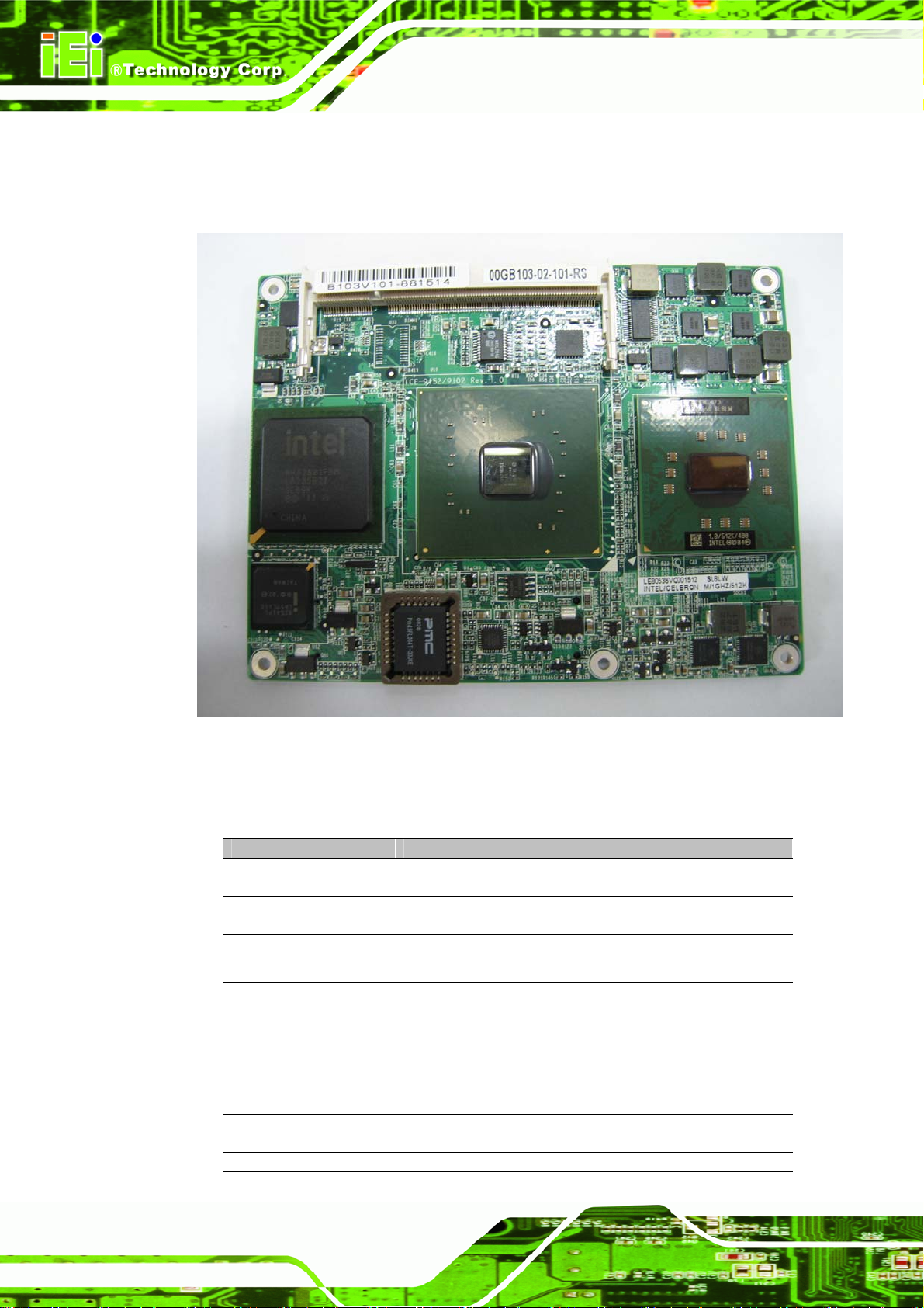
2.2.1 ICE-9152-R10
The ICE-9152 is shown in Figure 2-2 and the specifications are list in Table 2-2.
ICE Module
Figure 2-2: ICE-9152-R10
Table 2-2: ICE-9152-R10 Specification
Item Description
CPU Socket 479 Intel® Pentium® M, Celeron® M processor
with a 533/400MHz FSB
System Memory One 200-pin 533/400MHz DDR2 SDRAM SO-DIMM
supported (system max. 2GB)
System Chipset
BIOS AMI Flash BIOS
WatchDog Timer
Expansion Interface
MIO
USB 8 x USB 2.0 (Signal to Base Board)
Intel® 915GME + ICH6M
255 levels timer interval, from 1 to 255 sec or min
setup by software, jumperless selection, generates
system reset
1 x PCIe x16 signal to Base Board
4 x PCIe x1 signal to Base Board
4 x PCI , 32 bit / 33 MHz PCI bus Singal to Base Base
Board
2 x SATA (Signal to Base Board)
1 x IDE channel (Signal to Base Board)
Page 8
Page 22
ICE Module
Audio
Ethernet
CRT Display mode
LCD Display mode
Dimensions (L x W) 125 mm x 95 mm
Power Supply Voltage ATX / AT supported
Operating
Temperature
Operating Humidity 0% ~ 90% relative humidity, non-condensing
AC’97 Audio Signal to Base Board (Audio Codec on
Base Board)
One Intel® 82541PI GbE Chipset (co-layout Intel®
82551ER 10/100Mbps Ethernet chipset)
Signal to Base Board
VGA Integrated in Intel 915GME Signal (Signal to Base
Board)
18/24-bit Dual channel LVDS Signal (to Base Board)
0 ~ 60˚ C (32 ~ 140˚ F)
Page 9
Page 23
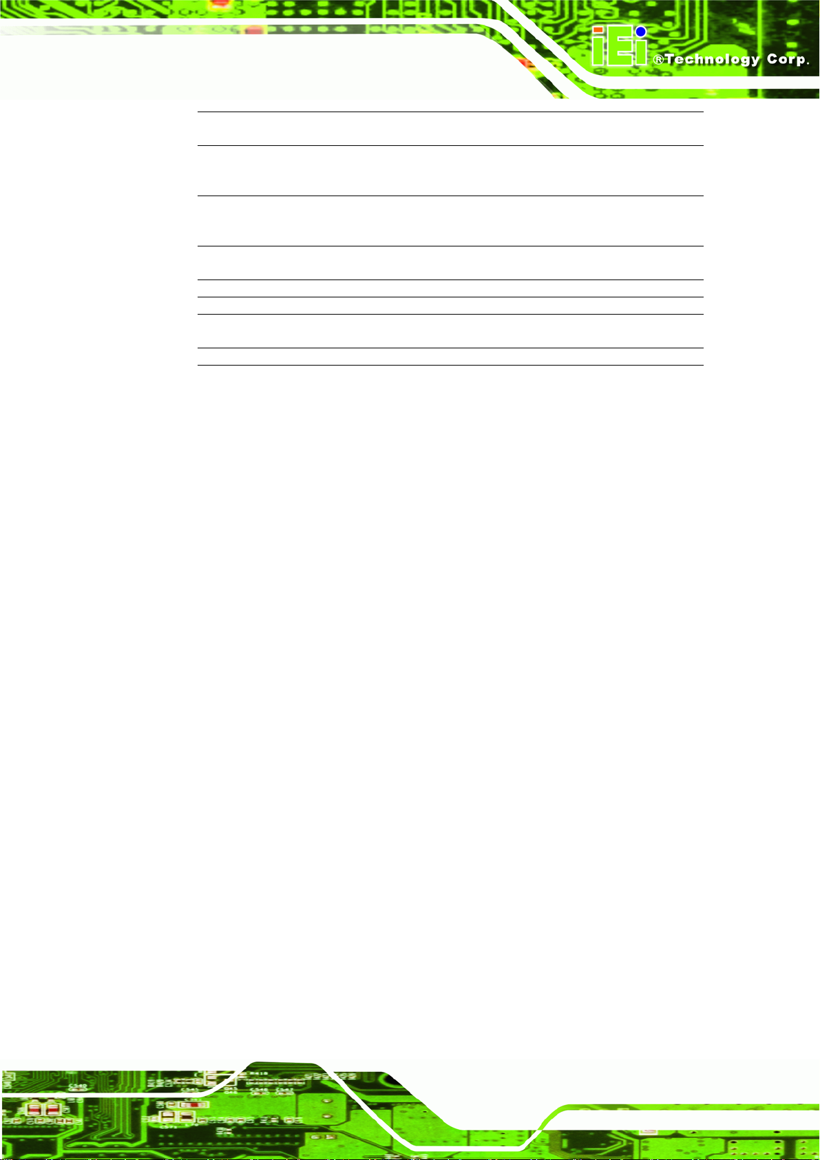
2.2.2 ICE-9102-1GZ-R10
The ICE-9102-1GZ is shown in Figure 2-3 and the specifications are listed in Table
2-3.
ICE Module
Figure 2-3: ICE-9102-1GZ-R10
Table 2-3: ICE-9102-1GZ-R10 Specification
Item Description
CPU On board Intel® Celeron® M 1GHz zero cache
processor
System Memory One 200-pin 400MHz DDR2 SDRAM SO-DIMM
supported (system max. 2GB)
System Chipset
BIOS AMI Flash BIOS
WatchDog Timer
Expansion Interface
MIO
USB 8 x USB 2.0 (Signal to Base Board)
Audio
Ethernet
Intel® 910GMLE + ICH6-M
Software programmable supports 1 ~255 sec. System
reset
2 x SATA (Signal to Base Board)
1 x IDE channel (Signal to Base Board)
4 x PCIe x1 Signal to Base Board
4 x PCI , 32 bit / 33 MHz PCI bus Signal to Base Board
AC’97 Audio Signal to Base Board (Audio Codec on
Base Board)
One Intel® 82541PI GbE Chipset (co-layout Intel®
82551ER 10/100Mbps Ethernet chipset)
Page 10
Page 24

ICE Module
Singal to Base Board
CRT Display mode
LCD Display mode
Dimensions (L x W) 125 mm x 95 mm
Power Supply Voltage ATX / AT supported
Operating
Temperature
Operating Humidity 0% ~ 90% relative humidity, non-condensing
VGA Integrated in Intel 910GMLE Signal (Signal to
Base Board)
18/24-bit Dual channel LVDS Signal (Signal to Base
Board)
0 ~ 60˚ C (32 ~ 140˚ F)
Page 11
Page 25

A
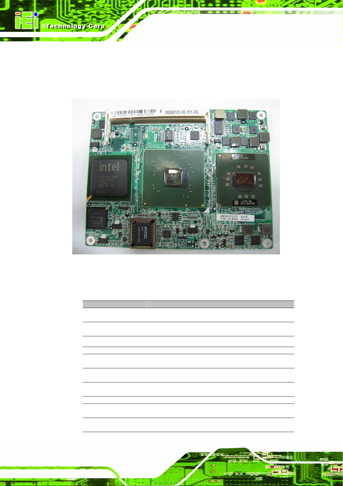
2.2.3 ICE-9102-1G512-R10
The ICE-9152-1G512 is shown in Figure 2-4 and the specifications are listed in Table
2-4.
ICE Module
Figure 2-4: ICE-9102-1G512-R10
Table 2-4: ICE-9102-1G512-R10 Specification
Item Description
CPU On board Intel® Celeron® M 1GHz 512KB cache
processor
System Memory One 200-pin 400MHz DDR2 SDRAM SO-DIMM
supported (system max. 2GB)
Intel® 910GMLE + ICH6-M
Software programmable supports 1 ~255 sec. System
reset
2 x SATA (Signal to Base Board)
1 x IDE channel (Signal to Base Board)
4 x PCIe x1 Signal to Base Board
4 x PCI , 32 bit / 33 MHz PCI bus Signal to Base Board
C’97 Audio Signal to Base Board (Audio Codec on
Page 12
System Chipset
BIOS AMI Flash BIOS
WatchDog Timer
Expansion Interface
MIO
USB 8 x USB 2.0 (Signal to Base Board)
Audio
Page 26

ICE Module
Base Board)
One Intel® 82541PI GbE Chipset (co-layout Intel®
Ethernet
CRT Display mode
LCD Display mode
Dimensions (L x W) 125 mm x 95 mm
Power Supply Voltage ATX / AT supported
Operating
Temperature
Operating Humidity 0% ~ 90% relative humidity, non-condensing
82551ER 10/100Mbps Ethernet chipset)
Signal to Base Board
VGA Integrated in Intel 910GMLE Signal (Signal to
Base Board)
18/24-bit Dual channel LVDS Signal (Signal to Base
Board)
0 ~ 60˚ C (32 ~ 140˚ F)
Page 13
Page 27
A
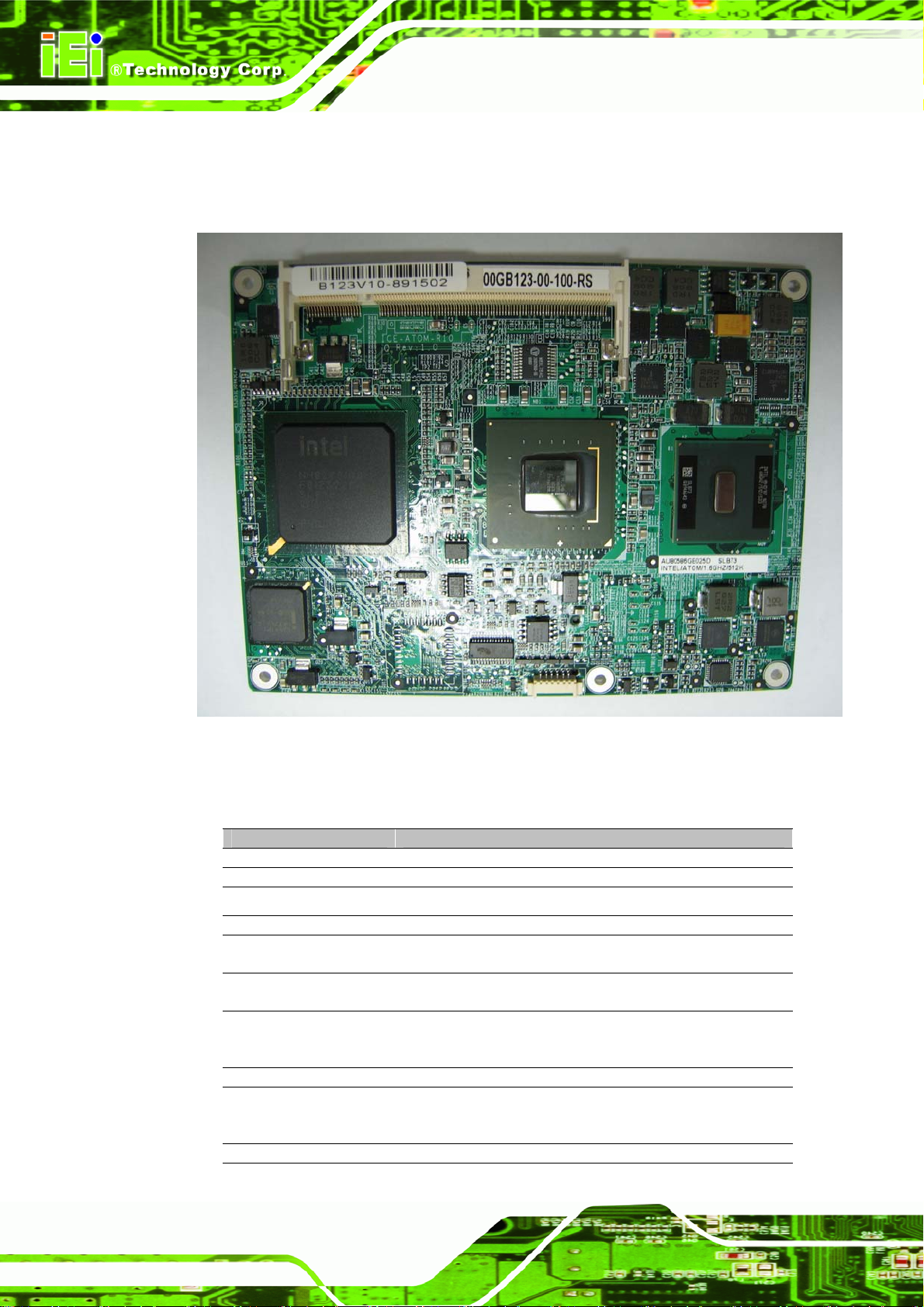
2.2.4 ICE-ATOM-R10
The ICE-ATOM is shown in Figure 2-5 and the specifications are listed in Table 2-5.
ICE Module
Figure 2-5: ICE-ATOM-R10
Table 2-5: ICE-ATOM-R10 Specification
Item Description
CPU Intel Diamondville-SC support at FSB 533Mhz
System Memory 1x DDR2 SO-DIMM 400/533MHz support up to 2GB
System Chipset
BIOS AMI BIOS
WatchDog Timer
Audio
MIO
USB 8 USB ports, USB 2.0 (Signal to Base Board)
Ethernet
Display
Intel 945GSE + ICH7M
Sofware Programmable support 1~255 sec. System
reset
HD Audio Signal to Base Board (Audio Codec on Base
Board)
2 x SATA II (Signal to Base Board)
1 x IDE channel (Signal to Base Board)
1 x Intel® 82541PI GbE Chipset (co-layout Intel®
82551ER 10/100Mbps Ethernet chipset) (Signal to
Base Board)
nalog CRT(VGA) Integrated in Intel® 945GSE (Signal
Page 14
Page 28

ICE Module
to Base Board)
18-bits Dual Channel LVDS Signal (Signal to Base
Board)
HDTV-out (Signal to Base Board)
1 x SDVO Interface (Only SDVO Port_B)
Dimensions (L x W) 125 mm x 95 mm
Power Supply Voltage AT/ATX support
Operating
Temperature
Operating Humidity 0% ~ 90% relative humidity, non-condensing system
0 ~ 60° C (32 ~ 140° F)
Page 15
Page 29

2.2.5 ICE-GM45A-R10
The ICE-GM45A is shown in Error! Reference source not found. and the specifications
ICE Module
are listed in
Table 2-6: ICE-GM45A-R10 Specification
Item Description
CPU Socket P Intel® mobile Core™ 2 Duo(Penryn), Intel®
System Memory 2 x 200-pins 1066/800MHz DDR2 SDRAM SO-DIMM
System Chipset
BIOS AMI BIOS
WatchDog Timer
Audio
MIO
Expansion
USB 8 x USB 2.0 (Signal to Base Board)
Ethernet 1 x Intel 82574L GbE chipset (Signal to Base Board)
Display
Dimensions (L x W) 125 mm x 95 mm
Power Supply Voltage ATX/AT supported
Operating
Temperature
Operating Humidity 0% ~ 90% relative humidity, non-condensing system
Table 2-6.
Celeron® M
Supported
Intel® GM45 + Intel® ICH9M
Software programmable supports 1 ~255 sec. System
reset
HD Audio Signal to Base Board (Audio Codec on Base
Board)
4 x SATA II (Signal to Base Board)
1 x IDE channel (Signal to Base Board)
1 x PCIe x16 signal to Base Board
4 x PCIe x1 signal to Base Board
4 x PCI, 32 bit / 33 MHz PCI bus to Base Board
Analog CRT(VGA) Integrated in Intel® GM45 (Signal to
Base Board)
18/24-bits Dual-Channel LVDS (Signal to Base Board)
HDTV-out (Signal to Base Board)
0 ~ 60° C (32 ~ 140° F)
Page 16
Page 30
ICE Module
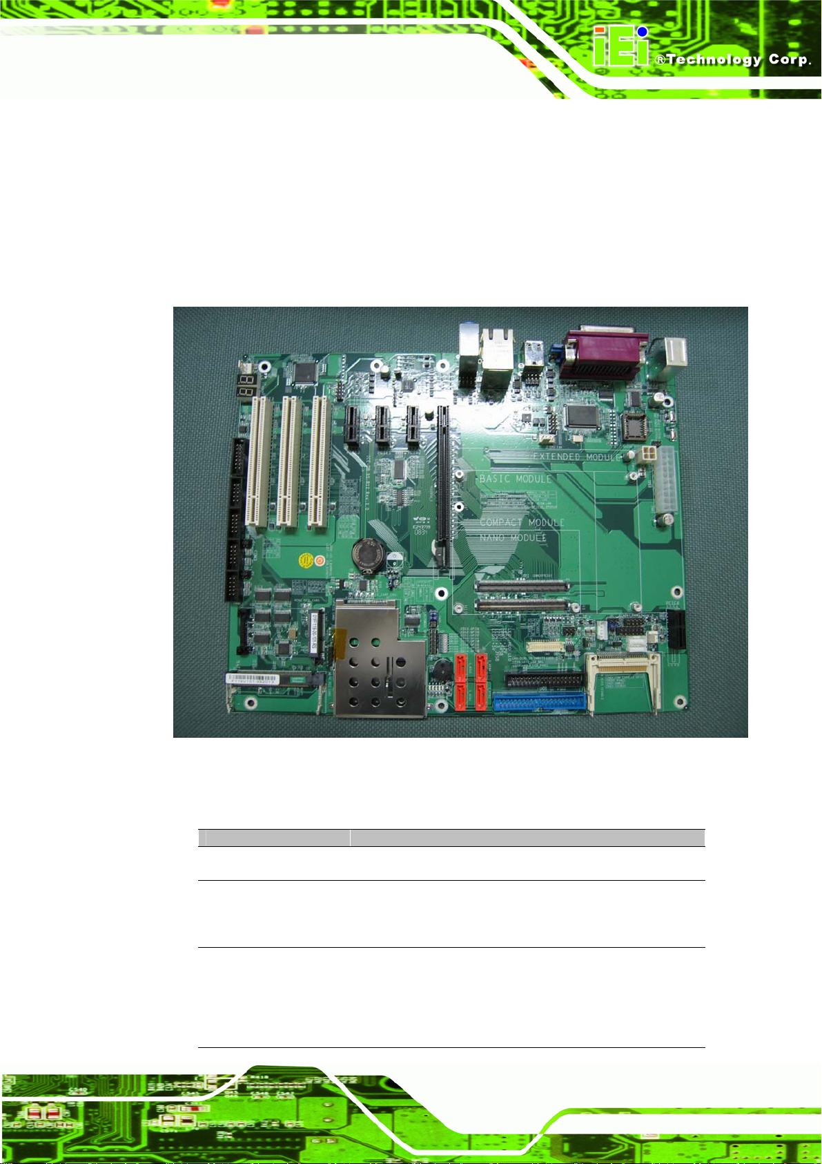
2.2.6 ICE-DB-9S-R10
The ICE-DB-9S is a full function carrier board for customers to apply or test the COM
Express module. The carrier board can be used for any combination, including
software and hardware. Using the carrier board to develop and test the ICE module
also can achieve a quicker time to market. The ICE-DB-9S is shown in
the specifications are listed in
Table 2-7.
Figure 2-6 and
Figure 2-6: ICE-DB-9S-R10
Table 2-7: ICE-DB-9S-R10 Specification
Item Description
CPU module interface Supports COM Express Compact/Basic/Extended
modules using connector pin out Type 2
Realtek ALC888 7.1 channels HD audio codec
Audio
MIO
Front Audio by pin-header(Line in, Line out, Mic in)
SPDIF by pin-header
CD-IN by pin-header
1 x PCIe by 16 Slot
4 x PCIe by 1 Slot
3 x PCI Slot
1 x PCIe Mini card Slot
1 x Express Card Slot
1 x Mini PCI Card Slot
Page 17
Page 31

1 x ISA
1 x IDE
2/4 x SATA/SATA II
1 x CF type II Slot
6 x USB 2.0
1 x LPT
1 x FDD
5 x RS-232
1 x RS-232/422/485
2 x USB 2.0 to PCIe Mini card Slot & Express Card Slot
Ethernet 1 x RJ-45 GbE connector
VGA DB15 connector
Display
Dimensions (L x W) 304.8 mm x 190.5 mm ( 12" x 7.5" )
Power Supply Voltage ATX / AT support
Operating
Temperature
Operating Humidity 0% ~ 90% relative humidity, non-condensing system
1 x 18/24 bit dual channel LVDS Connector
1 x Inverter connector
1 x TV-out interface
0 ~ 60° C (32 ~ 140° F)
ICE Module
Page 18
Page 32

ICE Module
2.3 Performance
Page 19
Page 33

ICE Module
Chapter
3
3 Pin Assignments
Page 20
Page 34

ICE Module
3.1 Chapter Overview
This chapter describes pin assignments and I/O characteristics for COM Express
modules. The carrier board uses two 220-pin 0.5 mm fine pitch board-to-board
connectors. There are five different pin-out types currently defined by the COM
Express Specification. The preferred choice of the embedded computer industry is the
Type 2 pin-out and therefore the leading manufacturers have chosen to produce COM
Express Type 2 modules. This pin-out offers the best balance between older
technology such as PCI and Parallel ATA while providing the latest technologies
including PCI Express, Serial ATA and PCI Express graphics.
Figure 3-1: COM Express Type 2 Module Diagram
Page 21
Page 35

3.2 Type 1, Type 2, Type 3, Type 4 and Type 5
The differences among the Module Types are summarized in Table 3-1.
Module Type 1 supports a single connector with two rows of pins
(220 pins total).
Module Types 2-5 support two connectors with four rows of pins
(440 pins total).
Connector placement and most mounting holes have transparency between Form
Factors.
Table 3-1
Module Type Rows PCIe Lanes (max) PCI IDE LAN (Max)
ICE Module
1
2 (Default)
3
4
5
AB 6 X X 1
AB, CD 22 V V 1
AB, CD 22 X V 3
AB, CD 32 V X 1
AB, CD 32 X X 3
Page 22
Page 36

ICE Module
3.3 Signal Table Terminology
The following section describes the signals found on COM Express Type 2 connectors.
Most of the signals listed in the following sections also apply to other COM Express
module types. The pinout for connector rows A and B remains the same regardless of
the module type but the pinout for connector rows D and C are dependent on the
module type. Refer to the COM Express specification for information about the
different pin-outs of the module types other than Type 2.
Table 3-2 below describes the terminology used in this section for the Signal
Description tables. The “#” symbol at the end of the signal name indicates that the
active or asserted state occurs when the signal is at a low voltage level. When “#” is
not present, the signal is asserted when at a high voltage level.
Table 3-2: Conventions and Terminology
Term Description
I/O Bi-directional signal
I Input signal
O Output signal
I/F Interface
GND Ground
PWR Power
OD Open drain output
PD Pull down
PU Pull up
+V12 +12V ±5% Volts Normal Power
+V5SB +5V ±5% Standby Power
+3.3VSB +3.3V ±5% Standby Power
+V3.3 +3.3V ±5% Volts Normal Power
+V5 +5V ±5% Volts Normal Power
# Active-Low Signals
‘+’ and ‘-‘ Differential Pairs
PM Power Management
GBE Giga Bits Ethernet
Page 23
Page 37

ICE Module
3.4 Connector Pinout Row A and Row B
Table 3-3: Module Type 2 Connector Pinout Rows (A and B)
Pin Signal I/F I/O Pin Signal I/F I/O
A1 GND GND - B1 GND GND -
A2 GBE0_MDI3- GBE I/O B2 GBE0_ACT# GBE O 3.3V
A3 GBE0_MDI3+ GBE I/O B3 LPC_FRAME# LPC O 3.3V
A4 GBE0_LINK100# GBE O 3.3V B4 LPC_AD0 LPC I/O 3.3V
A5 GBE0_LINK1000# GBE O 3.3V B5 LPC_AD1 LPC I/O 3.3V
A6 GBE0_MDI2- GBE I/O B6 LPC_AD2 LPC I/O 3.3V
A7 GBE0_MDI2+ GBE I/O B7 LPC_AD3 LPC I/O 3.3V
A8 GBE0_LINK# GBE O 3.3V B8 LPC_DRQ0# LPC I 3.3V
A9 GBE0_MDI1- GBE I/O B9 LPC_DRQ1# LPC I 3.3V
A10 GBE0_MDI1+ GBE I/O B10 LPC_CLK LPC O 3.3V
A11 GND GND - B11 GND GND -
A12 GBE0_MDI0- GBE I/O B12 PWRBTN# PM I
A13 GBE0_MDI0+ GBE I/O B13 SMB_CK SMB -
A14 GBE0_CTREF GBE B14 SMB_DAT SMB -
A15 SUS_S3# PM O B15 SMB_ALERT# SMB I
A16 SATA0_TX+ SATA O B16 SATA1_TX+ SATA O
A17 SATA0_TX- SATA O B17 SATA1_TX- SATA O
A18 SUS_S4# PM O B18 SUS_STAT# PM O
A19 SATA0_RX+ SATA I B19 SATA1_RX+ SATA I
A20 SATA0_RX- SATA I B20 SATA1_RX- SATA I
A21 GND GND - B21 GND GND -
A22 SATA2_TX+ SATA O B22 SATA3_TX+ SATA O
A23 SATA2_TX- SATA O B23 SATA3_TX- SATA O
A24 SUS_S5# PM O B24 PWR_OK PM I
A25 SATA2_RX+ SATA I B25 SATA3_RX+ SATA I
A26 SATA2_RX- SATA I B26 SATA3_RX- SATA I
A27 BATLOW# PM I B27 WDT - -
A28 ATA_ACT# SATA O 3.3V B28 AC_SDIN2 HDA I 3.3V
A29 AC_SYNC HDA O 3.3V B29 AC_SDIN1 HDA I 3.3V
A30 AC_RST# HDA O 3.3V B30 AC_SDIN0 HDA I 3.3V
A31 GND GND - B31 GND GND -
A32 AC_BITCLK HDA O 3.3V B32 SPKR - -
A33 AC_SDOUT HAD O 3.3V B33 I2C_CK I2C -
A34 BIOS_DISABLE# - - B34 I2C_DAT I2C -
A35 THRMTRIP# PM O B35 THRM# PM I
A36 USB6- USB I/O B36 USB7- USB I/O
A37 USB6+ USB I/O B37 USB7+ USB I/O
A38 USB_6_7_OC# USB I 3.3V B38 USB_4_5_OC# USB I 3.3V
A39 USB4- USB I/O B39 USB5- USB I/O
A40 USB4+ USB I/O B40 USB5+ USB I/O
A41 GND GND - B41 GND GND -
A42 USB2- USB I/O B42 USB3- USB I/O
A43 USB2+ USB I/O B43 USB3+ USB I/O
A44 USB_2_3_OC# USB I 3.3V B44 USB_0_1_OC# USB I 3.3V
A45 USB0- USB I/O B45 USB1- USB I/O
A46 USB0+ USB I/O B46 USB1+ USB I/O
A47 VCC_RTC PWR -- B47 EXCD1_PERST# PCIE -
A48 EXCD0_PERST# PCIE - B48 EXCD1_CPPE# PCIE -
A49 EXCD0_CPPE# PCIE - B49 SYS_RESET# PM I
A50 LPC_SERIRQ LPC I/O
3.3V
B50 CB_RESET# PM O
Page 24
Page 38

ICE Module
A51 GND GND - B51 GND GND -
A52 PCIE_TX5+ PCIE O B52 PCIE_RX5+ PCIE I
A53 PCIE_TX5- PCIE O B53 PCIE_RX5- PCIE I
A54 GPI0 - - B54 GPO1 - -
A55 PCIE_TX4+ PCIE O B55 PCIE_RX4+ PCIE I
A56 PCIE_TX4- PCIE O B56 PCIE_RX4- PCIE I
A57 GND GND - B57 GPO2 --
A58 PCIE_TX3+ PCIE O B58 PCIE_RX3+ PCIE I
A59 PCIE_TX3- PCIE O B59 PCIE_RX3- PCIE I
A60 GND GND - B60 GND GND -
A61 PCIE_TX2+ PCIE O B61 PCIE_RX2+ PCIE I
A62 PCIE_TX2- PCIE O B62 PCIE_RX2- PCIE I
A63 GPI1 - - B63 GPO3 - -
A64 PCIE_TX1+ PCIE O B64 PCIE_RX1+ PCIE I
A65 PCIE_TX1- PCIE O B65 PCIE_RX1- PCIE I
A66 GND GND - B66 WAKE0# PCIE I
A67 GPI2 - - B67 WAKE1# PM I
A68 PCIE_TX0+ PCIE O B68 PCIE_RX0+ PCIE I
A69 PCIE_TX0- PCIE O B69 PCIE_RX0- PCIE I
A70 GND GND - B70 GND GND -
A71 LVDS_A 0+ LV DS O B71 LVDS _B0+ LV DS O
A72 LVDS_A 0- LVDS O B72 LVDS_B 0- LVDS O
A73 LVDS_A 1+ LV DS O B73 LVDS _B1+ LV DS O
A74 LVDS_A 1- LVDS O B74 LVDS_B 1- LVDS O
A75 LVDS_A 2+ LV DS O B75 LVDS _B2+ LV DS O
A76 LVDS_A 2- LVDS O B76 LVDS_B 2- LVDS O
A77 LVDS_VDD_EN LVDS O 3.3V B77 LVDS_B 3+ LVDS O
A78 LVDS_A 3+ LV DS O B78 LVDS _B3- LV DS O
A79 LVDS_A 3- LVDS O B79 LVDS_BKLT_EN LVDS O 3.3V
A80 GND GND - B80 GND GND -
A81 LVDS_A _CK+ LVDS O B81 LV DS_ B_CK+ LVDS O
A82 LVDS_A _CK- LV DS O B82 LVDS_B_ CK- LVD S O
A83 LVDS_I2C_CK LVDS O 3.3V B83 LVDS_BKLT_CTRL LVDS O 3.3V
A84 LVDS_I2C_DAT LVDS IO 3.3V B84 5VSB PWR -
A85 GPI3 - - B85 5VSB PWR -
A86 KBD_RST# KB/MS B86 5VSB PWR -
A87 KBD_A20GATE B87 5VSB PWR -
A88 PCIE0_CK_REF+ B88 RSVD - -
A89 PCIE0_CK_REF- B89 VGA_RED VGA
A90 GND B90 GND GND -
A91 RSVD - - B91 VGA_GRN VGA
A92 RSVD - - B92 VGA_BLU VGA
A93 GPO0 B93 VGA_HSYNC VGA
A94 RSVD - - B94 VGA_VSYNC VGA
A95 RSVD - - B95 VGA_I2C_CK VGA
A96 GND GND B96 VGA_I2C_DAT VGA
A97 +V12 PWR - B97 TV_DAC_A TV
A98 +V12 PWR - B98 TV_DAC_B TV
A99 +V12 PWR - B99 TV_DAC_C TV
A100 GND GND B100 GND GND -
A101 +V12 PWR - B101 +V12 PWR -
A102 +V12 PWR - B102 +V12 PWR -
A103 +V12 PWR - B103 +V12 PWR -
A104 +V12 PWR - B104 +V12 PWR -
A105 +V12 PWR - B105 +V12 PWR -
A106 +V12 PWR - B106 +V12 PWR -
Page 25
Page 39

A107 +V12 PWR - B107 +V12 PWR -
A108 +V12 PWR - B108 +V12 PWR -
A109 +V12 PWR - B109 +V12 PWR -
A110 GND GND - B110 GND GND -
ICE Module
3.5 Connector Pinout Rows C and D
Table 3-4: Module Type 2 Connector Pinout Rows (C and D)
Pin Signal I/F I/O Pin Signal I/F I/O
C1 GND GND - D1 GND GND -
C2 IDE_D7 IDE IO 3.3V D2 IDE_D5 IDE IO 3.3V
C3 IDE_D6 IDE IO 3.3V D3 IDE_D10 IDE IO 3.3V
C4 IDE_D3 IDE IO 3.3V D4 IDE_D11 IDE IO 3.3V
C5 IDE_D15 IDE IO 3.3V D5 IDE_D12 IDE IO 3.3V
C6 IDE_D8 IDE IO 3.3V D6 IDE_D4 IDE IO 3.3V
C7 IDE_D9 IDE IO 3.3V D7 IDE_D0 IDE IO 3.3V
C8 IDE_D2 IDE IO 3.3V D8 IDE_REQ IDE I 3.3V
C9 IDE_D13 IDE IO 3.3V D9 IDE_IOW# IDE O 3.3V
C10 IDE_D1 IDE IO 3.3V D10 IDE_ACK# IDE O 3.3V
C11 GND GND - D11 GND GND -
C12 IDE_D14 IDE IO 3.3V D12 IDE_IRQ IDE I 3.3V
C13 IDE_IORDY IDE I 3.3V D13 IDE_A0 IDE O 3.3V
C14 IDE_IOR# IDE O 3.3V D14 IDE_A1 IDE O 3.3V
C15 PCI_PME# PCI IO 3.3V D15 IDE_A2 IDE O 3.3V
C16 PCI_GNT2# PCI O 3.3V D16 IDE_CS1# IDE O 3.3V
C17 PCI_REQ2# PCI I 3.3V D17 IDE_CS3# IDE O 3.3V
C18 PCI_GNT1# PCI O 3.3V D18 IDE_RESET# IDE IO 3.3V
C19 PCI_REQ1# PCI I 3.3V D19 PCI_GNT3# PCI O 3.3V
C20 PCI_GNT0# PCI O 3.3V D20 PCI_REQ3# PCI I 3.3V
C21 GND GND - D21 GND GND -
C22 PCI_REQ0# PCI I 3.3V D22 PCI_AD1 PCI IO 3.3V
C23 PCI_RESET# PCI O 3.3V D23 PCI_AD3 PCI IO 3.3V
C24 PCI_AD0 PCI IO 3.3V D24 PCI_AD5 PCI IO 3.3V
C25 PCI_AD2 PCI IO 3.3V D25 PCI_AD7 PCI IO 3.3V
C26 PCI_AD4 PCI IO 3.3V D26 PCI_C/BE0# PCI IO 3.3V
C27 PCI_AD6 PCI IO 3.3V D27 PCI_AD9 PCI IO 3.3V
C28 PCI_AD8 PCI IO 3.3V D28 PCI_AD11 PCI IO 3.3V
C29 PCI_AD10 PCI IO 3.3V D29 PCI_AD13 PCI IO 3.3V
C30 PCI_AD12 PCI IO 3.3V D30 PCI_AD15 PCI IO 3.3V
C31 GND GND - D31 GND GND -
C32 PCI_AD14 PCI IO 3.3V D32 PCI_PAR PCI IO 3.3V
C33 PCI_C/BE1# PCI IO 3.3V D33 PCI_SERR# PCI IO 3.3V
C34 PCI_PERR# PCI IO 3.3V D34 PCI_STOP# PCI IO 3.3V
C35 PCI_LOCK# PCI IO 3.3V D35 PCI_TRDY# PCI IO 3.3V
C36 PCI_DEVSEL# PCI IO 3.3V D36 PCI_FRAME# PCI IO 3.3V
C37 PCI_IRDY# PCI IO 3.3V D37 PCI_AD16 PCI IO 3.3V
C38 PCI_C/BE2# PCI IO 3.3V D38 PCI_AD18 PCI IO 3.3V
C39 PCI_AD17 PCI IO 3.3V D39 PCI_AD20 PCI IO 3.3V
C40 PCI_AD19 PCI IO 3.3V D40 PCI_AD22 PCI IO 3.3V
C41 GND GND - D41 GND GND -
C42 PCI_AD21 PCI IO 3.3V D42 PCI_AD24 PCI IO 3.3V
C43 PCI_AD23 PCI IO 3.3V D43 PCI_AD26 PCI IO 3.3V
C44 PCI_C/BE3# PCI IO 3.3V D44 PCI_AD28 PCI IO 3.3V
C45 PCI_AD25 PCI IO 3.3V D45 PCI_AD30 PCI IO 3.3V
Page 26
Page 40

ICE Module
C46 PCI_AD27 PCI IO 3.3V D46 PCI_IRQC# PCI I 3.3V
C47 PCI_AD29 PCI IO 3.3V D47 PCI_IRQD# PCI I 3.3V
C48 PCI_AD31 PCI IO 3.3V D48 PCI_CLKRUN# PCI I/O 3.3V
C49 PCI_IRQA# PCI I 3.3V D49 PCI_M66EN PCI I 3.3V
C50 PCI_IRQB# PCI I 3.3V D50 PCI_CLK PCI OI 3.3V
C51 GND GND - D51 GND GND -
C52 PEG_RX0+ PEG I D52 PEG_TX0+ PEG O
C53 PEG_RX0- PEG I D53 PEG_TX0- PEG O
C54 TYPE0# D54 PEG_LANE_RV#
C55 PEG_RX1+ PEG I D55 PEG_TX1+ PEG O
C56 PEG_RX1- PEG I D56 PEG_TX1- PEG O
C57 TYPE1# D57 TYPE2#
C58 PEG_RX2+ PEG I D58 PEG_TX2+ PEG O
C59 PEG_RX2- PEG I D59 PEG_TX2- PEG O
C60 GND GND - D60 GND GND -
C61 PEG_RX3+ PEG I D61 PEG_TX3+ PEG O
C62 PEG_RX3- PEG I D62 PEG_TX3- PEG O
C63 RSVD - - D63 RSVD - -
C64 RSVD - - D64 RSVD - -
C65 PEG_RX4+ PEG I D65 PEG_TX4+ PEG O
C66 PEG_RX4- PEG I D66 PEG_TX4- PEG O
C67 FAN_PWMOUT - O D67 GND GND -
C68 PEG_RX5+ PEG I D68 PEG_TX5+ PEG O
C69 PEG_RX5- PEG I D69 PEG_TX5- PEG O
C70 GND GND - D70 GND GND -
C71 PEG_RX6+ PEG I D71 PEG_TX6+ PEG O
C72 PEG_RX6- PEG I D72 PEG_TX6- PEG O
C73 SDVO_DATA D73 SVDO_CLK
C74 PEG_RX7+ PEG I D74 PEG_TX7+ PEG O
C75 PEG_RX7- PEG I D75 PEG_TX7- PEG O
C76 GND GND - D76 GND GND -
C77 FAN_TACHOIN - I D77 IDE_CBLID# IDE I 3.3V
C78 PEG_RX8+ PEG I D78 PEG_TX8+ PEG O
C79 PEG_RX8- PEG I D79 PEG_TX8- PEG O
C80 GND GND - D80 GND GND -
C81 PEG_RX9+ PEG I D81 PEG_TX9+ PEG O
C82 PEG_RX9- PEG I D82 PEG_TX9- PEG O
C83 RSVD D83 RSVD
C84 GND GND - D84 GND GND -
C85 PEG_RX10+ PEG I D85 PEG_TX10+ PEG O
C86 PEG_RX10- PEG I D86 PEG_TX10- PEG O
C87 GND GND - D87 GND GND -
C88 PEG_RX11+ PEG I D88 PEG_TX11+ PEG O
C89 PEG_RX11- PEG I D89 PEG_TX11- PEG O
C90 GND GND - D90 GND GND -
C91 PEG_RX12+ PEG I D91 PEG_TX12+ PEG O
C92 PEG_RX12- PEG I D92 PEG_TX12- PEG O
C93 GND GND - D93 GND GND -
C94 PEG_RX13+ PEG I D94 PEG_TX13+ PEG O
C95 PEG_RX13- PEG I D95 PEG_TX13- PEG O
C96 GND GND - D96 GND GND -
C97 RSVD - - D97 PEG_ENABLE#
C98 PEG_RX14+ PEG I D98 PEG_TX14+ PEG O
C99 PEG_RX14- PEG I D99 PEG_TX14- PEG O
C100 GND GND - D100 GND GND -
C101 PEG_RX15+ PEG I D101 PEG_TX15+ PEG O
Page 27
Page 41

C102 PEG_RX15- PEG I D102 PEG_TX15- PEG O
C103 GND GND - D103 GND GND -
C104 +V12 PWR - D104 +V12 PWR -
C105 +V12 PWR - D105 +V12 PWR -
C106 +V12 PWR - D106 +V12 PWR -
C107 +V12 PWR - D107 +V12 PWR -
C108 +V12 PWR - D108 +V12 PWR -
C109 +V12 PWR - D109 +V12 PWR -
C110 GND GND - D110 GND GND -
ICE Module
Page 28
Page 42

ICE Module
Chapter
4
4 Signal Description and
Routing Guideline
Page 29
Page 43

4.1 PEG (PCI Express Graphic)
The PEG Port can utilize COM Express PCIe lanes 16-32 and is suitable to drive a x16
link for an external high-performance PCI Express Graphics card, if implemented on
the COM Express module. It supports a theoretical bandwidth of up to 4 GB/s – twice
the peak bandwidth achievable with AGP 8x. Each lane of the PEG Port consists of a
receiver and transmit differential signal pair designated 'PEG_RX0' (+ and -) to
'PEG_RX15' (+ and -) and correspondingly from 'PEG_TX0' (+ and -) to 'PEG_TX15'
(+ and -). The corresponding signals can be found on the Module connector rows C
and D. The pins of the PEG Port are shared with other functionality like SDVO or DVO
depends of the used chipset. SDVO and PEG are defined on COM Express
specification as “may be used”. Please be sure, your functionality will be supported by
your module vendor.
4.1.1 Signal Description
ICE Module
Table 4-1: PCI Express Signal Descriptions
Pin Signal I/O Description
C52
C53
D52
D53
C55
C56
D55
D56
C58
C59
D58
D59
C61
C62
D61
D62
C65
C66
D65
D66
C68
C69
D68
D69
C71
C72
D71
D72
C74
C75
D74 PEG_TX7+ O PEG Port 7. Transmit Output differential pair.
PEG_RX0+
PEG_RX0PEG_TX0+
PEG_TX0PEG_RX1+
PEG_RX1PEG_TX1+
PEG_TX1PEG_RX2+
PEG_RX2PEG_TX2+
PEG_TX2PEG_RX3+
PEG_RX3PEG_TX3+
PEG_TX3PEG_RX4+
PEG_RX4PEG_TX4+
PEG_TX4PEG_RX5+
PEG_RX5PEG_TX5+
PEG_TX5PEG_RX6+
PEG_RX6PEG_TX6+
PEG_TX6PEG_RX7+
PEG_RX7-
I PEG Port 0. Receive Input differential pair.
O PEG Port 0. Transmit Output differential pair.
I PEG Port 1. Receive Input differential pair.
O PEG Port 1. Transmit Output differential pair.
I PEG Port 2. Receive Input differential pair.
O PEG Port 2. Transmit Output differential pair.
I PEG Port 3. Receive Input differential pair.
O PEG Port 3. Transmit Output differential pair.
I PEG Port 4. Receive Input differential pair.
O PEG Port 4. Transmit Output differential pair.
I PEG Port 5. Receive Input differential pair.
O PEG Port 5. Transmit Output differential pair.
I PEG Port 6. Receive Input differential pair.
O PEG Port 6. Transmit Output differential pair.
I PEG Port 7. Receive Input differential pair.
Page 30
Page 44

ICE Module
D75 PEG_TX7C78
C79
D78
D79
C81
C82
D81
D82
C85
C86
D85
D86
C88
C89
D88
D89
C91
C92
D91
D92
C94
C95
D94
D95
C98
C99
D98
D99
C101
C102
D101
D102
A88
A98
D73 SDVO_I2C_CLK O 2.5V
C73 SDVO_I2C_DAT
D54 PEG_LANE_RV# I 3.3V
D97 PEG_ENABLE# I 3.3V
PEG_RX8+
PEG_RX8PEG_TX8+
PEG_TX8PEG_RX9+
PEG_RX9PEG_TX9+
PEG_TX9PEG_RX10+
PEG_RX10PEG_TX10+
PEG_TX10PEG_RX11+
PEG_RX11PEG_TX11+
PEG_TX11PEG_RX12+
PEG_RX12PEG_TX12+
PEG_TX12PEG_RX13+
PEG_RX13PEG_TX13+
PEG_TX13PEG_RX14+
PEG_RX14PEG_TX14+
PEG_TX14PEG_RX15+
PEG_RX15PEG_TX15+
PEG_TX15PCIE_CLK_REF
+
PCIE_CLK_REF-
A
I PEG Port 8,. Receive Input differential pair.
O PEG Port 8. Transmit Output differential pair.
I PEG Port 9,. Receive Input differential pair.
O PEG Port 9. Transmit Output differential pair.
I PEG Port 10.. Receive Input differential pair.
O PEG Port 10.Transmit Output differential pair.
I PEG Port 11. Receive Input differential pair.
O PEG Port 11. Transmit Output differential pair.
I PEG Port 12. Receive Input differential pair.
O PEG Port 12. Transmit Output differential pair.
I PEG Port 13,. Receive Input differential pair.
O PEG Port 13. Transmit Output differential pair.
I PEG Port 14.. Receive Input differential pair.
O PEG Port 14. Transmit Output differential pair.
I PEG Port 15. Receive Input differential pair.
O PEG Port 15. Transmit Output differential pair.
O PCIe Reference Clock for all COM Express
CMOS
I/O 2.5V
OD CMOS
CMOS
CMOS
PCIe lanes, and for PEG lanes
I2C based control signal (clock) for SDVO
device.
I2C based control signal (data) for SDVO device
PCI Express Graphics lane reversal input strap.
Pull low on the carrier board to reverse lane
order.
PEG enable function. Strap to enable PCI
Express x16 external graphics interface. Pull low
to disable internal graphics and enable the x16
interface.
PS: IEI Bios auto detect the SDVO or
PCIEX16, please reserve for future use
Page 31
Page 45

4.1.2 PEG Connector
Figure 4-1 illustrates the pinout definition for the standard PCI Express x16
connectors.
ICE Module
+V3.3_DU AL
SMB_CK3,4,5, 10,11,17, 20
SMB_DAT3,4,5, 10,11,17, 20
PCIE_WAKE_U P#3,5,10,16
PEG_TX0+3
PEG_TX0-3
SDVO_I2C_CK3
PEG_TX1+3
PEG_TX1-3
PEG_TX2+3
PEG_TX2-3
PEG_TX3+3
PEG_TX3-3
SDVO_I2C_D AT3
PEG_TX4+3
PEG_TX4-3
PEG_TX5+3
PEG_TX5-3
PEG_TX6+3
PEG_TX6-3
PEG_TX7+3
PEG_TX7-3
PEG_TX8+3
PEG_TX8-3
PEG_TX9+3
PEG_TX9-3
PEG_TX10+3
PEG_TX10-3
PEG_TX11+3
PEG_TX11-3
PEG_TX12+3
PEG_TX12-3
PEG_TX13+3
PEG_TX13-3
PEG_TX14+3
PEG_TX14-3
PEG_TX15+3
PEG_TX15-3
+V12 +V3.3
PCIEX16_1
TP43
B10
B11
B12
B13
B14
B15
B16
B17
B18
B19
B20
B21
B22
B23
B24
B25
B26
B27
B28
B29
B30
B31
B32
B33
B34
B35
B36
B37
B38
B39
B40
B41
B42
B43
B44
B45
B46
B47
B48
B49
B50
B51
B52
B53
B54
B55
B56
B57
B58
B59
B60
B61
B62
B63
B64
B65
B66
B67
B68
B69
B70
B71
B72
B73
B74
B75
B76
B77
B78
B79
B80
B81
B82
B1
B2
B3
B4
B5
B6
B7
B8
B9
+12V03
+12V04
RSVD05
GND35
SMBCLK
SMBDATA
GND36
3_3V03
JTAG1
3_3VAUX
WAKE#
RSVD06
GND37
HSOP0
HSON0
GND38
PRSNT2#01
GND39
HSOP1
HSON1
GND40
GND41
HSOP2
HSON2
GND42
GND43
HSOP3
HSON3
GND44
RSVD07
PRSNT2#02
GND45
HSOP4
HSON4
GND46
GND47
HSOP5
HSON5
GND48
GND49
HSOP6
HSON6
GND50
GND51
HSOP7
HSON7
GND52
PRSNT2#03
GND53
HSOP8
HSON8
GND54
GND55
HSOP9
HSON9
GND56
GND57
HSOP10
HSON10
GND58
GND59
HSOP11
HSON11
GND60
GND61
HSOP12
HSON12
GND62
GND63
HSOP13
HSON13
GND64
GND65
HSOP14
HSON14
GND66
GND67
HSOP15
HSON15
GND68
PRSNT2#04
RSVD08
NC1
PCIE_X16
NC2
NC1
NC2
PRSNT1#
+12V01
+12V02
GND01
JTAG2
JTAG3
JTAG4
JTAG5
3_3V01
3_3V02
PWRGD
GND02
REFCLK+
REFCLK-
GND03
HSIP0
HSIN0
GND04
RSVD01
GND05
HSIP1
HSIN1
GND06
GND07
HSIP2
HSIN2
GND08
GND09
HSIP3
HSIN3
GND10
RSVD02
RSVD03
GND11
HSIP4
HSIN4
GND12
GND13
HSIP5
HSIN5
GND14
GND15
HSIP6
HSIN6
GND16
GND17
HSIP7
HSIN7
GND18
RSVD04
GND19
HSIP8
HSIN8
GND20
GND21
HSIP9
HSIN9
GND22
GND23
HSIP10
HSIN10
GND24
GND25
HSIP11
HSIN11
GND26
GND27
HSIP12
HSIN12
GND28
GND29
HSIP13
HSIN13
GND30
GND31
HSIP14
HSIN14
GND32
GND33
HSIP15
HSIN15
GND34
A1
A2
A3
A4
A5
A6
A7
A8
A9
A10
A11
A12
A13
A14
A15
A16
A17
A18
A19
A20
A21
A22
A23
A24
A25
A26
A27
A28
A29
A30
A31
A32
A33
A34
A35
A36
A37
A38
A39
A40
A41
A42
A43
A44
A45
A46
A47
A48
A49
A50
A51
A52
A53
A54
A55
A56
A57
A58
A59
A60
A61
A62
A63
A64
A65
A66
A67
A68
A69
A70
A71
A72
A73
A74
A75
A76
A77
A78
A79
A80
A81
A82
+V12+V3.3
CB_RESET# 3,5, 10,11,14, 20
CLK100M_PCIEx16_SLOT+ 4
R1710_4 12
R2230_4 12
R2240_4 12
R2250_4 12
R2260_4 12
R2270_4 12
R2280_4 12
R3760_4 12
R3780_4 12
R3790_4 12
R3800_4 12
R3810_4 12
R3820_4 12
R3830_4 12
R3840_4 12
R3850_4 12
R3860_4 12
R3870_4 12
R3880_4 12
R3890_4 12
R3900_4 12
R3910_4 12
R3920_4 12
R3930_4 12
R3940_4 12
R3950_4 12
R3960_4 12
R3970_4 12
R3990_4 12
R4000_4 12
R4010_4 12
CLK100M_PCIEx16_SLOT- 4
PEG_RX0+ 3
PEG_RX0- 3
PEG_RX1+ 3
PEG_RX1- 3
PEG_RX2+ 3
PEG_RX2- 3
PEG_RX3+ 3
PEG_RX3- 3
PEG_RX4+ 3
PEG_RX4- 3
PEG_RX5+ 3
PEG_RX5- 3
PEG_RX6+ 3
PEG_RX6- 3
PEG_RX7+ 3
PEG_RX7- 3
PEG_RX8+ 3
PEG_RX8- 3
PEG_RX9+ 3
PEG_RX9- 3
PEG_RX10+ 3
PEG_RX10- 3
PEG_RX11+ 3
PEG_RX11- 3
PEG_RX12+ 3
PEG_RX12- 3
PEG_RX13+ 3
PEG_RX13- 3
PEG_RX14+ 3
PEG_RX14- 3
PEG_RX15+ 3
PEG_RX15- 3
1
TP61
1
TP62
1
TP63
1
TP68
1
TP71
1R3770_4 12
TP72
1
TP73
1
TP74
1
TP75
1
TP76
1
TP77
1
TP78
1
TP79
1
TP81
1
TP82
1
TP83
1
TP84
1
TP85
1
TP86
1
TP87
Figure 4-1: PCI Express x16 Slot Example
Page 32
Page 46

ICE Module
4.1.3 SDVO
The Serial Digital Video Out (SDVO) display ports are multiplexed over a subset of the
External Graphics Interface using PCI Express. Users can choose a manufacturer
approved by Intel® to convert the SDVO port to TV, LVDS, DVI or CRT connection. IEI
also provides cables and SDVO card for customer to use. Due to the fact that SDVO is
an Intel® defined interface, the number of supported SDVO devices is limited to
devices that are supported by the Intel® Graphics Video BIOS and Graphics Driver
software.
The COM Express Module graphics controller configures the PEG lines for SDVO
operation if it detects that COM Express signals SDVO_I2C_CLK and
SDVO_I2C_DATA are pulled high to 2.5V, and if the PEG_ENABLE# line is left
floating. IEI BIOS auto detects the SDVO or PCIEX16, please reserve for future use.
Table 4-2: PEG & S DVO Pin Assignment
Pin Signal SDVO Description
C52
C53
C55
C56
C58
C59
C68
C69
D52
D53
D55
D56
D58
D59
D61
D62
D65
D66
D68
D69
D71
D72
D74
D75
PEG_RX0+
PEG_RX0PEG_RX1+
PEG_RX1PEG_RX2+
PEG_RX2PEG_RX5+
PEG_RX5PEG_TX0+
PEG_TX0PEG_TX1+
PEG_TX1PEG_TX2+
PEG_TX2PEG_TX3+
PEG_TX3PEG_TX4+
PEG_TX4PEG_TX5+
PEG_TX5PEG_TX6+
PEG_TX6PEG_TX7+
PEG_TX7-
SDVO_TVCLKIN+
SDVO_TVCLKINSDVOB_INT+
SDVOB_INT-
SDVO_FLDSTALL+
SDVO_FLDSTALL-
SDVOB_INT+
SDVOB_INT-
SDVOB_RED+
SDVOB_REDSDVOB_GREEN+
SDVOB_GREENSDVOB_BLUE+
SDVOB_BLUESDVOB_CLK+
SDVOB_CLKSDVOC_RED+
SDVOC_REDSDVOC_GREEN+
SDVOC_GREENSDVOC_BLUE+
SDVOC_BLUESDVOC_CLK+
SDVOC_CLK-
SDVO TVOUT Synchronization Clock
differential pair.
SDVOB Input Interrupt differential pair.
SDVO Field Stall differential pair.
SDVOC Input Interrupt differential pair.
SDVO Channel B Red differential pair.
SDVO Channel B Green differential pair.
SDVO Channel B Blue differential pair.
SDVO Channel B Clock differential pair.
SDVO Channel C Red differential pair.
SDVO Channel C Green differential pair.
SDVO Channel C Blue differential pair.
SDVO Channel C Clock differential pair.
Table 4-3: Intel® SDVO Support Device List
Device Vander Application Link
Page 33
Page 47

CH7021A Chrontel SDTV / HDTV Transmitter http://www.chrontel.com
CH7308A Chrontel LVDS Transmitter http://www.chrontel.com
CH7307C Chrontel DVI Transmitter http://www.chrontel.com
CH7312 Chrontel DVI Transmitter http://www.chrontel.com
CX25905 Conexant DVI-D / TV / CRT Transmitter http://www.conexant.com
SiL1362/1364 Silicon Image DVI Transmitter http://www.siliconimage.com
SiL 1390 Silicon Image HDMI Transmitter http://www.siliconimage.com
ICE Module
4.1.4 PEG_ENABLE#
PEG_ENABLE# is defined on the COM Express connector as a method to configure
the COM Express PCIe lanes 16 through 32 on the C-D connector as a PCI Express
Graphics port, for use with an external graphics device. The usual effect of pulling
PEG_ENABLE# low is to disable the on-Module graphics engine. For some Modules,
it is possible to configure the Module such that the internal graphics engine remains
active, even when the external PEG interface is being used for a Carrier Board
graphics device. This is Module dependent. Check with your vendor. ICE Modules
implement the auto-detect function. So, please reserve this pin for future use.
4.1.5 PCI Express Test Points and Probing
IEI follows the suggestion provided by Intel® to preserve 0-Ω on the baseboard.
Additional test structures were not included in the simulation sweeps that this
guideline is based on. The inclusion of test points and probing structures has the
ability to impact the loss and jitter budgets of a PCI Express interconnect. This is not to
say that they cannot be tolerated. In general, test points and probe structures should
not introduce stubs on the differential pairs or cause significant deviation from the
recommendations given throughout this chapter. Existing vias, pads or pins should be
used wherever possible to accommodate such structures. Careful consideration must
be taken whenever additional probing structures are used.
Page 34
The PCI Express based specification requires the data eyes to be measured into a
50-Ω resistor terminated to ground. To facilitate the measurement, an additional test
structure may be required on a test board. This test structure should not be included in
a production board because it will affect the overall signal quality and resulting
margins. The three-pad test structure consists of the footprints of two resistors,
perpendicular to each other forming a “L” shape. The resistor package/footprint should
Page 48

ICE Module
be as small as possible, preferably 0402. To enable the test mode, a 50 Ω ±1%
resistor stuffing option is needed to break the path. This will force the transmitter port
to enter the compliance mode and begin transmitting the compliance packet.
Otherwise, use a 0-Ω resistor to continue the trace route to the Rx port. This will allow
normal operation of the device.
Figure 4-2: Intel Recommend Test Structure for PCI Express Data Eye Measurement
4.1.6 PCI Express Routing Guideline
4.1.6.1 Impedance Consideration
The PCI Express impedance considerations are listed in Table 4-4.
Table 4-4: PCI Express Impedance Consideration
Parameters Routing
Transfer Rate / PCIe Lane 2.5 Gbits/sec
Maximum signal line length (coupled traces) TX and RX path: 21.0 inches
Maximum signal length allowance on the
COM Express module "
Signal length allowance on the COM
Express carrier board "
Differential Impedance 100 Ohms +/-20%
Single-ended Impedance 55 Ohms +/-15%
Trace width (W) 5 mils (microstrip routing) (*)
Spacing between differential pairs (intra-pair)
(S)
Spacing between RX and TX pairs
(inter-pair) (s)
Spacing between differential pairs and Min. 50mils
TX and RX path: 5.15 inches
TX and RX path: 15.85 inches @
0.28dB/GHz/inch to PCIe device 9.00 inches
@ 0.28dB/GHz/inch to PCIe slot
4 mils (microstrip routing) (*)
Min. 20mils
Page 35
Page 49

high-speed periodic signals
Spacing between differential pairs and
low-speed non periodic signals
Length matching between differential pairs
(intra-pair)
Length matching between RX and TX pairs
(inter-pair)
Length matching between reference clock
differential pairs REFCLK+ and REFCLK(intra-pair)
Length matching between reference clock
pairs (inter-pair)
Reference plain GND referenced preferred
Spacing from edge of plane Min. 40mils
Via Usage
AC coupling capacitors
Min. 20mils
Max. 5mils
No strict electrical requirements. Keep
difference within a 3.0 inch delta to minimize
latency.
Max. 5mils
No electrical requirements.
Max. 2 vias per TX trace Max. 4 vias per RX
trace
The AC coupling capacitors for the TX lines
are incorporated on the COM Express
module. The AC coupling capacitors for RX
signal lines have to be implemented on the
customer COM Express" carrier board.
Capacitor type: X7R
ICE Module
4.1.6.2 AC Coupling Capacitors
TX AC coupling capacitor is already embedded in the ICE modules. Users only need
to add the RX AC coupling capacitor on the baseboard. The PCI Express specification
requires that each lane of a PCI Express link be AC coupled between the driver and
receiver. The specification allows for the AC coupling capacitors to be located either
on or off the die. However, it is anticipated that in most cases the AC coupling will be
separated from the die and in the form of discrete capacitors on the motherboard itself.
While the 0603 size capacitors are acceptable, size 0402 capacitors are strongly
encouraged. — The smaller package size reduces the series inductance. — The
smaller package size reduces the overall board area needed to place the capacitors.
Page 36
Page 50

ICE Module
ICE Module
AC Coupling Cap
Figure 4-3: PEG Lane Connection Topology Example
4.1.6.3 Routing Notices
PEG SLOT or SDVO Device
TX+
TX-
RX+
RX-
Each signal and its complement in a differential pair should be length
matched whenever possible on a segment-by-segment basis at the point
of discontinuity. Examples of segments might include breakout areas,
routes to connect vias, routes to connect an AC coupling capacitor, routes
to connect a connector, and so forth.
When trace length matching occurs, it should be made as close as
possible to the point where the length variation occurs, as shown in
4-4. For example, length matching in a chipset breakout area or connector
pin field should occur within the first 125 mils (3.175 mm) of the structure
that causes the length mismatch.
When serpentining is needed to match lengths, the trace spacing should
not become greater than two times the original spacing. The length of the
increased spacing should not be greater than three times the trace width.
See
Figure 4-4. In determining the overall length of a given signal in a
differential pair, use pad or pin edge-to-edge distances rather than the
total etch present, unless the amount of trace routing inside each pad is
identical. The amount of etch within a given pad is electrically part of the
Figure
pad itself. In other words, only the etch outside of the pad edge is relevant
to the overall length of a differential pair.
Page 37
Page 51

Preferred Routing
Alternative Routing
Bad Routing
ICE Module
Preferred Routing
Figure 4-4: PEG Layout Trace Example
4.2 PCI Express
Preferred Routing
Page 38
PCI Express provides a scalable, high-speed, serial I/O point-to-point bus connection.
A PCI Express lane consists of dual simplex channels, each implemented as a
low-voltage differentially driven transmit pair and receive pair. They are used for
simultaneous transmission in each direction. The bandwidth of a PCI Express link can
be scaled by adding signal pairs to form multiple lanes between two devices. The PCI
Express specification defines x1, x4, x8, x16, and x32 link widths. Each single lane
has a raw data transfer rate of 2.5Gbps @ 1.25GHz.
Page 52

ICE Module
The PCI Express interface of the COM Express Type 2 module consists of up to 6
lanes, each with a receive and transmit differential signal pair designated from
PCIE_RX0 (+ and -) to PCIE_RX5 (+ and -) and correspondingly from PCIE_TX0 (+
and -) to PCIE_TX5 (+ and -). According to the PCI Express specification, these six
lanes can be configured as several PCI Express x1 links or to a combined x4 link plus
two x1 links. These configuration possibilities are based on the COM Express
module's chipset capabilities.
4.2.1 Signal Description
Table 4-5: PCI Express Signal Descriptions
Pin Signal I/O Description
B68
B69
A68
A69
B64
B65
A64
A65
B61
B62
A61
A62
B58
B59
A58
A59
B55
B56
A55
A56
B52
B53
A52
A53
A88
A98
B66 WAKE0# I PCIE PCIe Wake Event: Sideband wake-up signal.
A49 EXCD0_CPPE# I 3.3V
B48 EXCD1_CPPE# I 3.3V
A48 EXCD0_PERST# O 3.3V
B47 EXCD1_PERST# O 3.3V
PCIE_RX0+
PCIE_RX0PCIE_TX0+
PCIE_TX0PCIE_RX1+
PCIE_RX1PCIE_TX1+
PCIE_TX1PCIE_RX2+
PCIE_RX2PCIE_TX2+
PCIE_TX2PCIE_RX3+
PCIE_RX3PCIE_TX3+
PCIE_TX3PCIE_RX4+
PCIE_RX4PCIE_TX4+
PCIE_TX4PCIE_RX5+
PCIE_RX5PCIE_TX5+
PCIE_TX5PCIE_CLK_REF+
PCIE_CLK_REF-
I PCIe Port 0. Receive Input differential pair.
O PCIe Port 0. Transmit Output differential pair.
I PCIe Port 1. Receive Input differential pair.
O PCIe Port 1. Transmit Output differential pair.
I PCIe Port 2,. Receive Input differential pair.
O PCIe Port 2. Transmit Output differential pair.
I PCIe Port 3.. Receive Input differential pair.
O PCIe Port 3. Transmit Output differential pair.
I PCIe Port 4. Receive Input differential pair.
O PCIe Port 4. Transmit Output differential pair.
I PCIe Port 5. Receive Input differential pair.
O PCIe Port 5. Transmit Output differential pair.
O PCIe Reference Clock for all COM Express
PCIe lanes, and for PEG lanes
ExpressCard capable card request, slot 1.
CMOS
ExpressCard capable card request, slot 2.
CMOS
ExpressCard reset, slot 1.
CMOS
ExpressCard reset, slot 2.
CMOS
Page 39
Page 53

4.2.2 PCI Express Slot X1
Table 4-5 illustrates the pinout definition for the standard x1, x4, x8 and x16 PCI
Express connectors. The dashed lines in the diagram depict where each different
ICE Module
connector type ends. An example of an x1 PCIe slot is shown in
+V12+V3.3
+V3.3_DU AL
PCIE1
B1
+12V03
B2
+12V04
B3
RSVD01
B4
GND05
B10
B11
B12
B13
B14
B15
B16
B17
B18
B5
B6
B7
B8
B9
SMBCLK
SMBDATA
GND06
3_3V03
JTAG1
3_3VAUX
WAKE#
RSVD02
GND07
HSOP0
HSON0
GND08
PRSNT2#
GND09
PCIE_X1
SMB_CK3,4,6, 10,11,17,20
SMB_DAT3,4,6, 10,11,17,20
PCIE_W AKE_UP#
PCIE_TX1+3
PCIE_TX1-3
Figure 4-5: PCI Express x1 Slot Example
4.2.3 Express Card Connector
Hot-swappable Express Cards come in a small form factor and are designed primarily
NC1
NC2
NC1
NC2
PRSNT1#
+12V01
+12V02
GND01
JTAG2
JTAG3
JTAG4
JTAG5
3_3V01
3_3V02
PWRGD
GND02
REFCLK+
REFCLK-
GND03
HSIP0
HSIN0
GND04
A1
A2
A3
A4
A5
A6
A7
A8
A9
A10
A11
A12
A13
A14
A15
A16
A17
A18
Figure 4-5 below.
+V3.3+V1 2
CB_RESET# 3, 6,10,11,14,20
CLK100M_PCIEx 1_SLOT2+ 4
CLK100M_PCIEx 1_SLOT2- 4
R1240_4 12
PCIE_R X1+ 3
R1250_4 12
1
TP90
1
TP91
PCIE_R X1- 3
for mobile computing. The card’s electrical interface is thru USB 2.0 or a single x1
PCIe link. Express Cards are the successor to Card Bus Cards (which are PCI-based).
Card Bus cards, in turn, are the successors to PCMCIA cards. All three formats are
defined by the PCMCIA Consortium.
ExpressCard is a small, modular add-in card designed to replace common PCMCIA
and PC Cards. It takes advantage of the scalable, high-bandwidth serial PCI Express
and USB 2.0 interfaces to provide much higher data rates. COM Express modules
offer support for up to two ExpressCard slots. More information about the
ExpressCard Standard can be found at
http://www.expresscard.org.
In addition to the signals of a PCI Express x1 link and a USB 2.0 link, the ExpressCard
interface requires the following control signals provided by the COM Express module.
The corresponding signals can be found on the module connector rows A and B.
Page 40
Page 54

ICE Module
CB_RESET#3, 6,10,11,14,20
+V3.3
+V3.3
+V3.3_Expres sCard
+V3.3_Expres sCard
+V3. 3
C29
C28
0.1UF
10U_8_X_6V3
+V1.5_ExpressCard
EC9
@150U_TNC_SMD_6.3V
+V3.3_Expres sCard
EC10
@150U_TNC_SMD_6.3V
C35
0.1U_4_Y _16V
C26 10U_ 8_X_6V3
Q1
GS1117-SOT223
<Output Curre nt Capability >
I
V_IN
V_OUT
V_OUT1
D
N
G
G
C37
0.1U_4_Y _16V
C36
10U_8_X_6V3
+V3.3
R7310K_4 1 2
R7410K_4 1 2
PERST#
VCC1.5/1A
O
4
R75
124 1%-RS
R76
24.9 1%-RS
+V3.3SB_Expres sCard
C38
0.1U_4_Y _16V
1
2
3
4
5
6
7
8
9
10
+V1.5
TPS2231
SYSR ST#
SHDN#
STBY#
3.3VIN 1
3.3VIN 2
3.3VOUT1
3.3VOUT2
PERST#
NC
GND
TPS2231
C30
10U_8_X_6V3
LED6
R350
+V3.3_Expres sCard
+V3.3_DUAL
+V1.5
+V3.3SB_Expres sCard
U3
20
1
OC#
RCLKEN
AUXIN
AUXOUT
1.5VIN 2
1.5VIN 1
1.5VOUT2
1.5VOUT1
CPPE#
CPUSB#
CLK100M_PCIEx 1_SLOT3+4
CLK100M_PCIEx 1_SLOT3-4
+V3.3_Express Card
+V3.3_Express Card
+V3.3SB_Express Card
+V1.5_Express Card
USB6+3
USB6-3
COMCHOKE_8_U SB
TP41
19
1
TP42
18
17
16
15
14
13
CPPE#
12
CPUSB#
11
PCIE_TX2+3
PCIE_TX2-3
PCIE_R X2+3
PCIE_R X2-3
SMB_DAT3,4,6, 10,11,17,20
SMB_CK3,4,6, 10,11,17,20
L2
4
3
1
2
C27
0.1U_4_Y _16V
CPPE#
PERST#
PCIE_WAKE_UP#
CPUSB#
+V3.3SB_Express Card
+V1.5_Express Card
+V1.5_Express Card
E_Card_CON1
P26
GND4
P25
PETp0
P24
PETn0
P23
GND3
P22
PERp0
P21
PERn0
P20
GND2
P19
REFCLK+
P18
REFCLK-
P17
CPPE#
P16
CLKREQ#
P15
+3.3V 2
P14
+3.3V 1
P13
PERST#
P12
+3.3V AUX
P11
WAKE#
P10
+1.5V
P9
SMB_DATA
P8
SMB_CLK
P7
RESERVED3
P6
RESERVED2
P5
RESERVED1
P4
CPUSB#
P3
USB_D+
P2
USB_D-
P1
GND1
Express Card connector
470_6
R360
470_6
A C
LEDRED _8_2
LED7
A C
LEDRED _8_2
1
H
1
2
H
H
2
H
Figure 4-6: Express Card Slot Example
Table 4-6: Express Card Pin Definition
Pin Signal I/O Description
1 GND P Ground
2 USB_D- I/O USB USB Serial Data Interface differential pair, negative signal
3 USB_D+ I/O USB USB Serial Data Interface differential pair, positive signal
4 CPUSB# I 3.3V USB Interface presence detected
5 RSVD Reserved
6 RSVD Reserved
7 SMBCLK I/O 3.3V System Management Bus Clock
8 SMBDATA I/O 3.3V System Management Bus Data
9 +1.5V P 1.5V Secondary voltage source, 1.5V
10 +1.5V P 1.5V Secondary voltage source, 1.5V
11 WAKE# I 3.3V
12 +3.3VAUX P 3.3V Auxiliary voltage source, 3.3V
13 PERST# I 3.3V PCI Express Reset
14 +3.3V P 3.3V Primary voltage source, 3.3V
15 +3.3V P 3.3V Primary voltage source, 3.3V
16 CLKREQ# I 3.3V Request that REFCLK be enabled
17 CPPE# I 3.3V PCI Express interface presence detect
18 REFCLK- I PCIe
19 REFCLK+ I PCIe PCI Express reference clock differential pair, positive signal
20 GND P Ground
21 PERn0 I/O PCIe PCI Express Receiver differential pair negative signal
22 PERp0 I/O PCIe PCI Express Receiver differential pair positive signal
Request that the host interface return to full operation and
respond to PCIe
PCI Express reference clock differential pair, negative
signal
Page 41
Page 55

23 GND P Ground
24 PETn0 I/O PCIe PCI Express Transmitter differential pair negative signal
25 PETp0 I/O PCIe PCI Express Transmitter differential pair positive signal
26 GND P Ground
The PCMCIA Consortium defines two form factors for Express Cards:
Express Card/34 and Express Card/54 use a socket-style interconnect.
There are two mechanical Form Factors with Express Card/34, which
are useable in either socket. Each has the same electrical interface.
Interface support for a PCIe x1 lane and USB 2.0 on the socket is
required.
Socket interface requirements for Carrier Boards include:
PCIe x1 Lane and USB 2.0
WAKE# and the SM Bus are optional at the socket and COM Express
Module level.
ICE Module
Figure 4-7: Express Card 54&34 Type (Refer to www.expresscard.org)
Page 42
Page 56

ICE Module
Figure 4-8: Express Card 54 & 34 Plug Way (Refer to www.expresscard.org)
4.2.4 PCIe Mini Card
The PCI Express Mini Card add-in card is a small size unique form factor optimized for
mobile computing platforms equipped with communication applications such as
Wireless LAN. A small footprint connector can be implemented on the carrier board
providing the ability to insert different removable PCI Express Mini Cards. Using this
approach gives the flexibility to mount an upgradeable, standardized PCI Express Mini
Card device to the carrier board without additional expenditure of a redesign. In
addition to a PCI Express x1 link and a USB 2.0 link, the PCI Express Mini Card
interface utilizes the following control and reset signals, which are provided by the
COM Express module connector rows A and B.
Page 43
Page 57

ICE Module
51
49
47
45
43
41
39
37
35
33
31
29
27
25
23
21
19
17
15
13
11
9
1
7
5
3
1
1
TP96
1
TP97
PCIE_R X3+3
PCIE_R X3-3
CLK33M_MINICAR D4
CB_RESET#3,6,10,11, 14,20
CLK100M_PCIEx1_SLOT4+4
CLK100M_PCIEx1_SLOT4-4
PCIE_W AKE_UP#3,6,10,16
CN1(LATCH)1
MINI PCIE LATCH_DIP
PCIE_TX3+3
PCIE_TX3-3
R1220_4 12
R1230_4 12
R700_4 12
R720_4 12
TP40
PCIE_W AKE_UP#
Figure 4-9: Express Card Slot Example
CN1
RESERVED _10
RESERVED _9
RESERVED _8
RESERVED _7
RESERVED _6
RESERVED _5
RESERVED _4
RESERVED _3
GND9
PETp0
PETn0
GND7
GND6
PERp0
PERn0
GND4
UIM_C4
UIM_C8
GND2
REFCLK+
REFCLKGND1
CLKREQ#
RESERVED _2
RESERVED _1
WAKE#
4
5
2
3.3V_2
G
GND11
1.5V_3
LED_WPAN #
LED_WLAN #
LED_W WAN#
GND10
USB_D+
USB_D-
GND8
SMB_DATA
SMB_CLK
1.5V_2
GND5
3.3VAUX1
PERST#
W_DI SABLE#
GND3
UIM_VPP
UIM_RESET
UIM_CLK
UIM_DATA
UIM_PWR
1.5V_1
GND0
3.3V_1
1
G
MINI PCIE CON_9MM_0.8
3
5
+V3.3
52
50
48
1
46
44
42
40
38
36
34
32
30
28
26
24
22
20
18
16
14
12
10
8
6
4
2
TP38
1
TP39
SMB_DAT
SMB_CK
CB_RESET#
+V1.5
L1 COMCHOKE_8_U SB
4
1
+V1.5
+V3.3_DUAL
R71 8.2K_4
+V1.5
+V3.3
3
USB7+ 3
2
USB7- 3
+V3.3
MINIC ARD_DISABLE# 13
LPC_AD0 3,11, 13,14,20
LPC_AD1 3,11, 13,14,20
LPC_AD2 3,11, 13,14,20
LPC_AD3 3,11, 13,14,20
LPC_FR AME# 3,11,13, 14,20
The following sections illustrate signal pin-outs for the system connector. Table 4-7
lists the pin-out for the system connector.
Table 4-7: Mini Card Pin-out
Pin # Signal Pin # Signal
51 Reserved* 52 +3.3V
49 Reserved* 50 GND
47 Reserved* 48 +1.5V
45 Reserved* 46 LED_WPAN#
43 Reserved* 44 LED_WLAN#
41 Reserved* 42 LED_WWAN#
39 Reserved* 40 GND
37 Reserved* 38 USB_D+
35 GND 36 USB_D33 PETp0 34 GND
31 PETn0 32 SMB_DATA
29 GND 30 SMB_CLK
27 GND 28 +1.5V
25 PERp0 26 GND
23 PERn0 24 +3.3Vaux
21 GND 22 PERST#
19 Reserved 20 Reserved***
17 Reserved 18 GND
15 GND 16 Reserved**
13 REFCLK+ 14 Reserved**
11 REFCLK- 12 Reserved**
9 GND 10 Reserved**
7 CLKREQ# 8 Reserved**
Mechanical Key
Page 44
Page 58

ICE Module
* Reserved for future second PCI Express Lane (if needed)
** Reserved for future Subscriber Identity Module (SIM) interface (if needed)
*** Reserved for future wireless disable signal (if needed)
**** Reserved for future wireless coexistence control interface (if needed)
5 Reserved**** 6 1.5V
3 Reserved**** 4 GND
1 WAKE# 2 3.3V
Figure 4-10: Mini Card Bottom Side Dimensions (Refer to www.pcisig.com)
Figure 4-11: Mini Card Top Side Dimensions (Refer to www.pcisig.com)
Page 45
Page 59

ICE Module
Figure 4-12: Mini Card Connector (Refer to www.pcisig.com)
4.2.5 PCI Express Clock Buffer
COM Express only provides a set of 100 MHz Clock for PCI Express Device. When
there are more than one PCI Express modules used on the baseboard, the Clock
Buffer must be used. Please refer to the schematic diagram (
by IEI.
+V3.3_C LK +V3. 3_CLK
CLK_DIV#
CLK100M_PCIE_R EF+3
CLK100M_PCIE_R EF-3
CLK100M_PCIE x1_SLOT1+5
CLK100M_PCIE x1_SLOT1-5
CLK100M_PCIE x1_SLOT2+5
CLK100M_PCIE x1_SLOT2-5
CLK100M_PCIE x1_SLOT3+5
CLK100M_PCIE x1_SLOT3-5
CLK100M_PCIE x1_SLOT4+5
CLK100M_PCIE x1_SLOT4-5
SMB_CK3,5,6,10,11, 17,20
SMB_DAT3,5,6,10, 11,17,20
R16 33_412
R18 33_412
R20 33_412
R21 33_412
R22 33_412
R23 33_412
R25 33_412
R27 33_412
CLK_OE_0
CLK_OE_3
CLK_OE_1
CLK_OE_2
CLK_PLL
1
2
3
4
5
6
7
8
9
10
11
12
13
14
15
16
17
18
19
20
21
22
23
24
U1
SRC_DIV#
VDD01
GND01
SRC_IN
SRC_IN#
OE_0
OE_3
DIF_0
DIF_0#
GND02
VDD02
DIF_1
DIF_1#
OE_1
OE_2
DIF_2
DIF_2#
GND03
VDD03
DIF_3
DIF_3#
BYPASS#/ PLL
SCLK
SDATA
ICS9DB801
VDDA
GNDA
IREF
LOCK
OE_7
OE_4
DIF_7
DIF_7#
OE_INV
VDD04
DIF_6
DIF_6#
OE_6
OE_5
DIF_5
DIF_5#
GND04
VDD05
DIF_4
DIF_4#
HIGH_BW#
SRC_SOP#
GND05
Figure 4-13) suggested
+V3.3 _CLK_ A
48
47
46
45
44
43
42
1
TP32
41
1
TP33
40
39
38
37
36
35
34
33
32
31
30
29
28
27
26
PD#
25
CLK_IR EF
CLK_LOCK
CLK_OE_7
CLK_OE_4
R114 33_412
R115 33_412
CLK_OE_6
CLK_OE_5
R112 33_412
R113 33_412
CLK_HBW#
CLK_SRC _SOP#
CLK_PD#
R10 475
CLK100M_PCIEx 1_SLOT6+ 10
CLK100M_PCIEx 1_SLOT6- 10
CLK100M_PCIEx 1_SLOT5+ 10
CLK100M_PCIEx 1_SLOT5- 10
R2433_4 1 2
R2633_4 1 2
CLK100M_PCIEx 16_SLOT+ 6
CLK100M_PCIEx 16_SLOT- 6
Figure 4-13: PCI Express Clock Buffer Example
4.2.5.1 PCI Express Routing Guideline
Please refer to Section 4.1.6
Page 46
Page 60

ICE Module
4.3 PCI
The COM Express provides a PCI Bus interface that is compliant with the PCI Local
Bus Specification, Revision 2.2. The implementation is optimized for high-performance
data streaming when the COM Express is acting as either the target or the initiator on
the PCI bus. For more information on the PCI Bus interface, refer to the PCI Local Bus
Specification, Revision 2.2.
4.3.1 Signal Description
Table 4-8 shows COM Express PCI bus signal, including pin number, signals, I/0,
power plane, terminal resistors, damping resistors and descriptions.
Table 4-8: PCI Signal Description
Pin Signal I/O Description
Note1 PCI_AD[0..31] I/O 3.3V PCI bus multiplexed address and data lines
Note1 PCI_C/BE[0..3]# I/O 3.3V PCI bus byte enable lines , active low
C36 PCI_DEVSEL# I/O 3.3V PCI bus Device Select, active low.
D36 PCI_FRAME# I/O 3.3V PCI bus Frame control line, active low.
C37 PCI_IRDY# I/O 3.3V PCI bus Initiator Ready control line, active low.
D35 PCI_TRDY# I/O 3.3V PCI bus Target Ready control line, active low.
D34 PCI_STOP# I/O 3.3V PCI bus STOP control line, active low.
D32 PCI_PAR I/O 3.3V PCI bus parity
C34 PCI_PERR# I/O 3.3V Parity Error: An external PCI device drives PERR# to
low, when it receives data that has a parity error.
Note1 PCI_REQ[0..3]# I 3.3V PCI bus master request input line, active low.
Note1 PCI_GNT[0..3]# O 3.3V PCI bus master grant output lines, active low.
C23 PCI_RESET# O 3.3V PCI Reset output, active low.
C35 PCI_LOCK# I/O 3.3V PCI Lock control line, active low.
D33 PCI_SERR# I/O 3.3V System Error: SERR# may be pulsed active by any
PCI device that detects a system error condition.
C15 PCI_PME# I 3.3VSB PCI Power Management Event: PCI peripherals drive
PME# to low to wake up the system from low-power
states S1–S5.
D48 PCI_CLKRUN# I/O 3.3V Bidirectional pin used to support PCI clock run
protocol for mobile systems.
Note1 PCI_IRQ[A..D]# I 3.3V PCI interrupt request lines.
D50 PCI_CLK O 3.3V PCI 33MHz clock output.
D49 PCI_M66EN I 3.3V Module input signal that indicates whether an carrier
board PCI device is capable of 66MHz operation. It is
pulled to ground by carrier board device or by slot
card, if one of the devices are NOT capable of
66MHz operation.
Please refer to Table 3-3: Module Type 2 Connector Pinout Rows (A and B) or
Table 3-4: Module Type 2 Connector Pinout Rows (C and D).
Page 47
Page 61

4.3.2 PCI Connector
The PCI slot connection is shown in Figure 4-14.
PCI_AD[0..31]3,8,9
R77 5.6K_4
PCI_INT#B3, 8
PCI_IN T#D3
CLK33M_SLOT14
PCI_R EQ#13
PCI_C /BE#33,8, 9
PCI_C /BE#23,8, 9
PCI_IRDY#3, 8,9
PCI_D EVSEL#3,8
PCI_LOC K#3
PCI_PERR#3,8
PCI_SER R#3,8
PCI_C /BE#13,8, 9
+V5
R85 8.2K_4
12
C51 0.1U_4_Y _16V
C50 0.1U_4_Y _16V
PCI_AD31
PCI_AD29
PCI_AD27
PCI_AD25
PCI_AD23
PCI_AD21
PCI_AD19
PCI_AD17
PCI_AD14
PCI_AD12
PCI_AD10
PCI_AD8
PCI_AD7
PCI_AD5
PCI_AD3
PCI_AD1
+V3. 3
+V5
-V12
B10
B11
B12
B13
B14
B15
B16
B17
B18
B19
B20
B21
B22
B23
B24
B25
B26
B27
B28
B29
B30
B31
B32
B33
B34
B35
B36
B37
B38
B39
B40
B41
B42
B43
B44
B45
B46
B47
B48
B49
B52
B53
B54
B55
B56
B57
B58
B59
B60
B61
B62
B1
B2
B3
B4
B5
B6
B7
B8
B9
PCI1
-12V
TCK
GND11
TDO
+5V07
+5V08
INTB#
INTD#
PRSNT1#01
RSVD03
PRSNT1#02
GND12
GND13
RSVD04
GND14
CLK
GND15
REQ#
+5V09
AD31
AD29
GND16
AD27
AD25
+3.3V0 7
C/BE3#
AD23
GND17
AD21
AD19
+3.3V0 8
AD17
C/BE2#
GND18
IRDY#
+3.3V0 9
DEVSEL#
GND19
LOCK#
PERR#
+3.3V1 0
SERR#
+3.3V1 1
C/BE1#
AD14
GND20
AD12
AD10
GND21
AD8
AD7
+3.3V1 2
AD5
AD3
GND22
AD1
+5V10
ACK64#
+5V11
+5V12
X1
TRS T#
+5V01
INTA#
INTC#
+5V02
RSVD
+5V03
RSVD02
GND01
GND02
3.3VAUX
RST#
+5V04
GNT#
GND03
PME#
AD30
+3.3V0 1
AD28
AD26
GND04
AD24
IDSEL
+3.3V0 2
AD22
AD20
GND05
AD18
AD16
+3.3V0 3
FRAME#
GND06
TRDY#
GND07
STOP#
+3.3V0 4
SMBCLK
SMDATA
GND08
AD15
+3.3V0 5
AD13
AD11
GND09
C/BE0#
+3.3V0 6
GND10
+5V05
REQ64#
+5V06
2
X
X1
PCISLOT120_2.54
2
X
+12V
TMS
PAR
AD9
AD6
AD4
AD2
AD0
TDI
+5V
A1
A2
A3
A4
A5
A6
A7
A8
A9
A10
A11
A12
A13
A14
A15
A16
A17
A18
A19
A20
A21
A22
A23
A24
A25
A26
A27
A28
A29
A30
A31
A32
A33
A34
A35
A36
A37
A38
A39
A40
A41
A42
A43
A44
A45
A46
A47
A48
A49
A52
A53
A54
A55
A56
A57
A58
A59
A60
A61
A62
+V12
+V5
+V3. 3
+V3.3_DU AL
PCI_PME#
PCI_AD 30
PCI_AD 28
PCI_AD 26
PCI_AD 24
1 2
R79 100_4_1%
PCI_AD 22
PCI_AD 20
PCI_AD 18
PCI_AD 16
PCI_AD 15
PCI_AD 13
PCI_AD 11
PCI_AD 9
PCI_AD 6
PCI_AD 4
PCI_AD 2
PCI_AD 0
R86 8.2K_4
ICE Module
PCI_INT#A 3,8
PCI_I NT#C 3
PCI_R ST# 3, 8,9,13
PCI_GN T#1 3
PCI_PME# 3,8
PCI_AD 20
PCI_F RAME# 3, 8,9
PCI_TRDY # 3,8
PCI_STOP# 3,8
R8110K_4
R8310K_4
PCI_PAR 3, 8
PCI_C/ BE#0 3,8,9
+V3. 3
+V5
Figure 4-14: PCI Slot Connection Example
4.3.3 PCI IRQ Assignment
Most of this PCI devices only utilize the interrupt signal 'INTA#'. To distribute the
interrupt source of the devices over the interrupt signals 'INTB#', 'INTC#' and 'INTD#',
an interrupt cross routing has to be implemented on the COM Express carrier board
design. Figure 5-14 and Table 5-16 illustrate the PCI bus interrupt routing for the PCI
bus slots 1-4. The PCI REQ and GNT lines with the same index must be considered
Page 48
Page 62

ICE Module
as a pair. It is not permitted to combine REQ and GNT lines with a different index. A
PCI REQ/GNT pair can only be used once for a single PCI bus-master device.
Table 4-9: PCI Slot Routing Table
Slot1 Slot2 Slot3 Slot4
IDSEL PCI_AD[20] PCI_AD[21] PCI_AD[22] PCI_AD[23]
INTA# PCI_IRQ[A]# PCI_IRQ[B]# PCI_IRQ[C]# PCI_IRQ[D]#
INTB# PCI_IRQ[B]# PCI_IRQ[C]# PCI_IRQ[D]# PCI_IRQ[A]#
INTC# PCI_IRQ[C]# PCI_IRQ[D]# PCI_IRQ[A]# PCI_IRQ[B]#
INTD# PCI_IRQ[D]# PCI_IRQ[A]# PCI_IRQ[B]# PCI_IRQ[C]#
Figure 4-15: PCI Slot Routing Example
Page 49
Page 63

4.3.4 PCI Clock Buffer
The COM Express Specification only supports a single PCI clock signal called
'PCI_CLK' to be used on the carrier board. If there are multiple devices or slots
implemented on the carrier board, a zero delay clock buffer is required to expand the
number of PCI clocks so that each device or each bus slot will be provided with a
separate clock signal.
PCI Clock Buffer
V 1.01 Modify
CLK33M_PCI3
CLK33M_MINIPCI8
CLK33M_SLOT37
CLK33M_80PORT9
CLK33M_BIOS220
CLK33M_TPM11
R37 33_412
R40 33_412
+V3.3_CLKBUF FER
R44 33_412
R47 33_412
CLKBUFFER_S2 CLKBUFFER _S1
R51 33_412
U2
1
REF
2
CLKA1
3
CLKA2
4
VDD
5
GND
6
CLKB1
7
CLKB2
S28S1
CY2309N ZSXC-1H
CLKOUT
CLKA4
CLKA3
VDD
GND
CLKB4
CLKB3
ICE Module
R34@33_41 2
16
15
14
13
12
11
10
9
R3833_4 1 2
R4133_4 1 2
+V3.3_CLKBUF FER
R4533_4 1 2
R4833_4 1 2
CLK33M_SLOT1 7
CLK33M_SLOT2 7
CLK33M_SIO2 14
CLK33M_MINICAR D 5
CLK33M_SLOT1
CLK33M_SLOT2
CLK33M_SLOT3
CLK33M_SIO2
CLK33M_BIOS2
CLK33M_TPM
CLK33M_MINICAR D
CLK33M_80PORT
CLK33M_MINIPCI
C10 10P_4_N _50V1 2
C11 10P_4_N _50V1 2
C13 10P_4_N _50V1 2
C241 10P_4_N_50V1 2
C265 10P_4_N_50V1 2
C266 10P_4_N_50V1 2
C267 10P_4_N_50V1 2
C14 10P_4_N _50V1 2
C12 10P_4_N _50V1 2
C15
10U_8_X_6V3
+V3.3
FB3
FB30_8_3A
10U_8_X_6V3
C16
C17
0.1U_4_Y _16V
C18
0.1U_4_Y _16V
+V3.3_CLKBUF FER
+V3.3_CLK
+V3.3_CLK
Figure 4-16: PCI Clock Buffer Example
4.3.5 PCI Routing Guideline
Particular attention must be paid to the PCI clock routing. The PCI Local Bus
specification requires a maximum propagation delay for the clock signals of 10ns
within a propagation skew of 2ns @ 33MHz between the several clock signals. The
COM Express Specification allows 1.6ns ± 0.1ns @ 33MHz propagation delay for the
PCI clock signal beginning from the module pin to the destination pin of the PCI device.
The propagation delay is dependent on the trace geometries, PCB stack-up and the
PCB dielectric constant. Calculating using a typical propagation delay value of
180ps/inch for an internal layer clock trace of the carrier board, a maximum trace
CLKBUFFER_S1
R6210K_4 1 2
R63@10K_4 1 2
CLKBUFFER_S2
R6510K_4 1 2
R67@10K_4 1 2
Page 50
length of 8.88 inches is allowed.
The clock trace from the COM Express module to a PCI bus slot should be 2.5 inches
shorter because PCI cards are specified to have 2.5 inches of clock trace length on
the card itself. PCI clock signals should be routed as a single ended trace with a trace
impedance of 55Ω. To reduce EMI, a single ground referenced internal layer is
recommended. The clock traces should be separated as far as possible from other
Page 64

ICE Module
signal traces. Refer to section 8.1 'PCI Trace Routing Guidelines' and the 'PCI Local
Bus Specification Revision 2.3' to get more information about this subject.
Table 4-10: PCI Impedance Consideration
Parameters Routing
Transfer Rate @ 33MHz 132 MB/sec
Signal length used on COM Express module
(including the COM Express" carrier board
connector) "
Maximum data and control signal length
allowance for the COM Express carrier board. "
Maximum clock signal length allowance for the
COM Express carrier board. "
Single-ended Impedance 55 Ohms +/-15%
Trace width (W) 5mils (microstrip routing) (*)
Spacing between signals (inter-signal) (S) 7mils (microstrip routing) (*)
Length matching between single ended signals Max. 200mils
Length matching between clock signals Max. 200mils
Spacing from edge of plane Min. 40mils
Reference plain GND referenced preferred
Via Usage Try to minimize number of vias
Decoupling capacitors for each PCI slot.
3.0 inches
10 inches
8.88 inches
Min. 1x22μF, 2x 100nF @ VCC 5V Min.
2x22μF, 4x 100nF @ VCC 3.3V Min.
1x22μF, 2x 100nF @ +12V (if used) Min.
1x22μF, 2x 100nF @ -12V (if used)
4.4 SATA (Serial ATA Interface)
Serial ATA is a serial interface for connecting storage devices (mainly hard disks) and
was defined to replace the old parallel ATA interface. SATA uses a point-to-point serial
connection between the system and the storage device. The first generation of
standard SATA provides a maximum effective data transfer rate of 150 MB/s per port.
With the second generation SATA II, an effective transfer rate of up to 300 MB/s per
port is possible. Serial ATA is completely software transparent to the IDE interface
while providing a lower pin count and higher performance.
4.4.1 Signal Description
All COM Express modules provide up to 4 Serial ATA channels, each with a receive
and transmit differential signal pair designated from 'SATA0_RX' (+ and -) to
'SATA3_RX' (+ and -) and correspondingly from 'SATA0_TX' (+ and -) to 'SATA3_TX'
(+ and -). The appropriate signals can be found on the COM Express module
connector row A and row B.
Page 51
Page 65

Table 4-11: Serial ATA Signal Descriptions
Pin Signal I/O Description
ICE Module
A19
A20
A16
A17
B19
B20
B16
B17
A25
A26
A22
A23
B25
B26
B22
B23
SATA0_RX+
SATA0_RXSATA0_TX+
SATA0_TXSATA1_RX+
SATA1_RXSATA1_TX+
SATA1_TXSATA2_RX+
SATA2_RXSATA2_TX+
SATA2_TXSATA3_RX+
SATA3_RXSATA3_TX+
SATA3_TX-
I SATA Serial ATA channel 0 Receive input differential pair.
O SATA Serial ATA channel 0 Transmit output differential pair.
I SATA Serial ATA channel 1 Receive input differential pair.
O SATA Serial ATA channel 1 Transmit output differential pair.
I SATA Serial ATA channel 2 Receive input differential pair.
O SATA Serial ATA channel 2 Transmit output differential pair.
I SATA Serial ATA channel 3 Receive input differential pair.
O SATA Serial ATA channel 3 Transmit output differential pair.
A28 SATA_ACT# O 3.3V
CMOS OC
4.4.2 SATA Connector
Serial ATA activity LED. Open collector output pin driven
during SATA command activity.
Each ICE module provides four SATA port at maximum. Users can use these SATA
ports for their applications.
Figure 4-17 shows the standard SATA port connection.
S_ATA1
SATA_1X7_1
8
9
S_ATA3
SATA_1X7_1
8
9
GND1
A+
8
GND2
9
B+
GND3
GND1
A+
8
GND2
9
B+
GND3
1
2
3
A-
4
5
B-
6
7
1
2
3
A-
4
5
B-
6
7
SATA0_TX+
SATA0_TX-
SATA0_RXSATA0_RX+
SATA1_TX+
SATA1_TX-
SATA1_RXSATA1_RX+
SATA0_TX+ 3
SATA0_TX- 3
SATA0_RX- 3
SATA0_RX+ 3
SATA1_TX+ 3
SATA1_TX- 3
SATA1_RX- 3
SATA1_RX+ 3
Figure 4-17: SATA 7-pin Connector Example
SATA_1X7_1
SATA_1X7_1
S_ATA2
GND1
8
9
GND2
GND3
S_ATA4
GND1
8
9
GND2
GND3
1
2
A+
8
3
A-
4
9
5
B-
6
B+
7
1
2
A+
8
3
A-
4
9
5
B-
6
B+
7
SATA2_TX+
SATA2_TX-
SATA2_RXSATA2_RX+
SATA3_TX+
SATA3_TX-
SATA3_RXSATA3_RX+
SATA2_TX+ 3
SATA2_TX- 3
SATA2_RX- 3
SATA2_RX+ 3
SATA3_TX+ 3
SATA3_TX- 3
SATA3_RX- 3
SATA3_RX+ 3
Page 52
Page 66

ICE Module
4.4.3 SATA LED#
The SATA LED can be used with the HDD LED. Please refer to the following
schematic diagram.
+V3. 3
R322
R323
4.7K
4.7K
HDD _LED#11,21
ATA_ACT#3, 21
HDD_LED#
D17
K1
1
K2
2
BAW56LT1_SOT23
Figure 4-18: SATA LED Connection Example
4.4.4 SATA Routing Guideline
C
3
LED1
LEDR ED_8_2
R324 470_6_5%
AC
+V5
Table 4-12: SATA Impedance Consideration
Parameters Routing
Transfer Rate 3.0 Gbits/sec
7.0 inches on PCB (COM Express module
Maximum signal line length (coupled traces)
and carrier board. The length of the SATA
cable is specified between 0 and 40 inches) "
Signal length used on COM Express module
(including the COM Express" carrier board
2.5 inches
connector) "
Signal length available for the COM Express
carrier board "
4.5 inches
Differential Impedance 100 Ohms +/-20%
Single-ended Impedance 55 Ohms +/-15%
Trace width (W) 5mils (microstrip routing) (*)
Spacing between differential pairs (intra-pair)
(S)
Spacing between RX and TX pairs
(inter-pair) (s)
Spacing between differential pairs and
high-speed periodic signals
Spacing between differential pairs and
low-speed non periodic signals
Length matching between differential pairs
(intra-pair)
7mils (microstrip routing) (*)
Min. 20mils
Min. 50mils
Min. 20mils
Max. 5mils
No strict electrical requirements. Keep
Length matching between RX and TX pairs
(inter-pair)
difference within a 3.0 inch delta to minimize
latency. Do not serpentine to meet trace
length guidelines for the RX and TX path.
Spacing from edge of plane Min. 40mils
Via Usage Try to minimize number of vias
The AC coupling capacitors for the TX and
AC Coupling capacitors
RX lines are incorporated on the COM
Express module. "
Page 53
Page 67

4.5 Universal Serial Bus (USB)
The Universal Serial Bus (USB) provides a bi-directional, isochronous, hot-attachable
Plug and Play serial interface for adding external peripheral devices such as game
controllers, communication devices and input devices on a single bus. A COM
Express Module must provide a minimum of four USB ports and can support up to
eight USB ports.
USB stands for Universal Serial Bus, an industry-standard specification for attaching
peripherals to a computer. It delivers high performance, the ability to plug in and
unplug devices while the computer is running, great expandability, and a wide variety
of solutions.
The USB physical topology consists of connecting the downstream hub port to the
upstream port of another hub or to a device. The USB can operate at three speeds.
ICE Module
High-speed (480 Mb/s) and full-speed (12 Mb/s) require the use of a shielded cable
with two power conductors and twisted pair signal conductors. Low-speed (1.5 Mb/s)
recommends, but does not require the use of a cable with twisted pair signal
conductors. The connectors are designed to be hot plugged. The USB Icon on the
plugs provides tactile feedback making it easy to obtain proper orientation.
4.5.1 Signal Description
Table 4-13 shows COM Express USB signals, including pin number, signals, I/0,
power plane, terminal resistors, damping resistors and descriptions.
Table 4-13: USB Signal Description
Pin Signal I/O Description
A46
A45
B46
B45
A43
A42
B43
B42
A40
A39
B40
B39
A37
A36
USB0+
USB0-
USB1+
USB1-
USB2+
USB2-
USB3+
USB3-
USB4+
USB4-
USB5+
USB5-
USB6+
USB6-
I/O USB Differential Data Port 0.
I/O USB Differential Data Port 1.
I/O USB Differential Data Port 2.
I/O USB Differential Data Port 3.
I/O USB Differential Data Port 4.
I/O USB Differential Data Port 5.
I/O USB Differential Data Port 6.
Page 54
Page 68

ICE Module
B37
B36
B44 USB_0_1_OC# I 3.3V CMOS USB over-current sense, USB ports 0 and 1. A pull-up for this
A44 USB_2_3_OC# I 3.3V CMOS USB over-current sense, USB ports 2 and3. A pull-up for this
B38 USB_4_5_OC# I 3.3V CMOS USB over-current sense, USB ports 4 and 5. A pull-up for this
USB7+
USB7-
I/O USB Differential Data Port 7.
line shall be present on the module. An open drain driver from
a USB current monitor on the Carrier Board may drive this
line low. Do not pull this line high on the Carrier Board.
line shall be present on the module. An open drain driver from
a USB current monitor on the Carrier Board may drive this
line low. Do not pull this line high on the Carrier Board.
line shall be present on the module. An open drain driver from
a USB current monitor on the Carrier Board may drive this
line low. Do not pull this line high on the Carrier Board.
4.5.2 USB Keyed Connector Protocol
To minimize end user termination problems, USB uses a “keyed connector” protocol.
The physical difference in the Series “A” and “B” connectors insures proper end user
connectivity. The “A” connector is the principle means of connecting USB devices
directly to a host or to the downstream port of a hub. All USB devices must have the
standard Series “A” connector specified in this chapter. The “B” connector allows
device vendors to provide a standard detachable cable. This facilitates end user cable
replacement.
Figure 4-19: Keyed Connector Protocol (Refer to USB2.0 Spec.)
Page 55
Page 69

ICE Module
The following list explains how the plugs and receptacles can be mated:
Series “A” receptacle mates with a Series “A” plug. Electrically, Series “A”
receptacles function as outputs from host systems and/or hubs.
Series “A” plug mates with a Series “A” receptacle. The Series “A” plug
always is oriented towards the host system.
Series “B” receptacle mates with a Series “B” plug (male). Electrically,
Series “B” receptacles function as inputs to hubs or devices.
Series “B” plug mates with a Series “B” receptacle. The Series “B” plug is
always oriented towards the USB hub or device.
USB connector usually used connector of Type A.
Figure 4-20: USB Connector
Table 4-14: USB Connector Signal Description
Pin Signal I/O Description
1 VCC P +5V Power supply
2 DATA- I/O USB Data, negative differential signal.
3 DATA+ I/O USB Data, positive differential signal.
4 GND P Ground
Page 56
Page 70

ICE Module
4.5.3 ESD/EMI
To improve the EMI behavior of the USB interface, a design should include common
mode chokes, which have to be placed as close as possible to the USB connector
signal pins. Common mode chokes can provide required noise attenuation but they
also distort the signal quality of full-speed and high-speed signaling. Therefore,
common mode chokes should be chosen carefully to meet the requirements of the
EMI noise filtering while retaining the integrity of the USB signals on the carrier board
design.
To protect the USB host interface of the module from over-voltage caused by
electrostatic discharge (ESD) and electrical fast transients (EFT), low capacitance
steering diodes and transient voltage suppression diodes have to be implemented on
the carrier board design.
USB0-_R USB1-_R
IO_GND
D10
1
2
3 4
PACDN006
6
+V5_USB01
5
USB1+_RUSB0+_R
Figure 4-21: RailClamp SRV05-4 Low Capacitance TVS Diode Array for ESD
USB1-_R
USB1+_R
COMCHOKE_8_USB
1
4
L17
2
3
USB1- 3
USB1+ 3
Figure 4-22: 90 ohm Common Mode Choke at 100MHz for EMI
Page 57
Page 71

4.5.4 Over Current Protection
Over-current protection for USB ports can be implemented by using power distribution
switches on the carrier board that monitor the USB port power lines. Power distribution
switches usually have a soft-start circuitry that minimizes inrush current in applications
where highly capacitive loads are employed. Transient faults are internally filtered.
Additionally, they offer a fault status output that is asserted during over-current and
thermal shutdown conditions. These outputs should be connected to the
corresponding COM Express modules USB over-current sense signals. IEI uses
MIC2026 for carrier board.
ICE Module
Figure 4-23: MIC2026 Block Diagram(Please refer the datasheet from MICREL )
4.5.5 Reference Schematics
The following notes apply to Figure 4-24 below.
LAN_USB and CN26 incorporate two USB Type A receptacles, LAN_USB in addition
includes an RJ-45 (LANKom LJ -G40BU1-10-F).
The reference design uses an over-current detection and protection device. The Micrel
MIC2026 is dual channel power distribution switch. Power to the USB Port is filtered
using a ferrite (30 Ω @100MHz, 600mA) to minimize emissions. The ferrite should be
placed adjacent to the USB Port connector pins. The OC# signal is asserted until the
over-current or over-temperature condition is resolved.
Page 58
Page 72

ICE Module
USB0+/- through USB4+/- from the COM Express Module are routed through a
common mode choke to reduce radiated cable emissions. The part shown is a AXIS
POWER BCCUB-T4P-2012-900T; this device has a common mode impedance of
approximately 90 Ω at 100MHz. The common-mode choke should be placed close to
the USB connector.
ESD protection diodes D10、D11 and D12 provide over-voltage protection caused by
ESD and electrical fast transients. Low capacitance diodes and transient voltage
suppression diodes should be placed near the USB connector. The example design
uses a RailClamp SRV05-4 low capacitance TVS Diode Array
(
http://www.semtech.com).
+V5_DUAL
R249
@0_4
ENB4OUTB
USB_0_1_OC#3
USB_2_3_OC#3
USB_4_5_OC#3
3
FLGB
2
FLGA
1
ENA
ENB4OUTB
3
FLGB
2
FLGA
1
ENA
ENB4OUTB
3
FLGB
2
FLGA
1
ENA
R375
0_4
MIC20 26
MIC20 26
MIC20 26
U31
5
6
GND
7
IN
8
OUTA
5
6
GND
7
IN
8
OUTA
U33
5
6
GND
7
IN
8
OUTA
USB Power control
1
C286
+
150U_TNC_SMD_6V3
2
1
C287
+
150U_TNC_SMD_6V3
2
C288
1
+
150U_TNC_SMD_6V3
2
C289
1
+
150U_TNC_SMD_6V3
2
C290
1
+
150U_TNC_SMD_6V3
2
C291
1
+
150U_TNC_SMD_6V3
2
FB6
GCB1608K-300
FB7
GCB1608K-300
FB8
GCB1608K-300
FB33
GCB1608K-300
FB36
GCB1608K-300
FB37
GCB1608K-300
+V5_USB 0
+V5_USB 1
+V5_USB 2
+V5_USB 3
+V5_USB 4
+V5_USB 5
USB Port0~6
USB0-3
USB0+3
USB2-3
USB2+3
USB4-3
USB4+3
COMCHOKE_8_USB
3
L16
COMCHOKE_8_USB
3
L18
COMCHOKE_8_USB
3
L19
+V5_USB01
+V5_USB01
+V5_USB23
+V5_USB23
+V5_USB45
+V5_USB45
+V5_USB0
USB0-_R
142
USB0+_R
+V5_USB2
142
142
C181 0.1U_4 _Y_16V
C182 0.1U_4 _Y_16V
C183 0.1U_4 _Y_16V
C184 0.1U_4 _Y_16V
C185 0.1U_4 _Y_16V
C186 0.1U_4 _Y_16V
IO_GND
IO_GND
USB2-_R
USB2+_R
+V5_USB4
USB4-_R
USB4+_R
LAN_USB1B
1
VCC1
2
D1-
3
D1+
4
GND1
LJ-G40BU1- 10
CN26
H3
U1
U2
U3
U4
H4 H6
IO_GND
1
3 4
5 6
HEADER_2X4_2.54
VCC2
D2D2+
GND2
5
H
USB1
5
U
U6
U7
U8
V1.01 Modif y
2
87
+V5_USB1
5
USB1-_R
6
USB1+_R
7
8
IO_GND
IO_GND
+V5_USB3
USB3-_R
USB3+_R
IO_GND
USB5+_R
USB5-_R
+V5_USB5
from Semtech
COMCHOKE_8_USB
142
USB1- 3
3
USB1+ 3
L17
COMCHOKE_8_USB
142
USB3- 3U32
3
USB3+ 3
L20
L21
3
USB5+ 3
142
USB5- 3
COMCHOKE_8_USB
USB for ESD Protect
D10
USB0-_R USB1-_R
1
6
+V5_USB 01
2
IO_GND
IO_GND
IO_GND
5
3 4
PACDN006
D11
USB2-_R USB3-_R
1
6
+V5_USB 23
2
5
USB2+_R
3 4
PACDN006
D12
USB4-_R USB5-_R
1
6
+V5_USB 45
2
5
USB4+_R
3 4
PACDN006
USB1+_RUSB0+_R
USB3+_R
USB5+_R
Figure 4-24: USB Reference Design
Page 59
Page 73

ICE Module
4.5.6 USB Routing Guideline
4.5.6.1 Impedance
Parameters Routing
Transfer rate / Port 480 Mbit/s
Maximum signal line length (coupled traces) Max. 17.0 inches
Signal length used on COM Express module (including the COM
Express" connector) "
Signal length allowance for the COM Express carrier board " 14.0 inches
Differential Impedance 90 Ohms +/-15%
Single-ended Impedance 45 Ohms +/-10%
Spacing between pairs-to-pairs (inter-pair) (s) Min. 20mils
Spacing between differential pairs and high-speed periodic
signals
Spacing between differential pairs and low-speed non periodic
signals
Reference plain GND referenced preferred
Spacing from edge of plane Min. 40mils
Via Usage Try to minimize number of
3.0 inches
Min. 50mils
Min. 20mils
vias
4.5.6.2 General Routing and Placement
USB 2.0 signals should be ground referenced.
Route USB 2.0 signals using a minimum of vias and corners. This reduces
reflections and impedance changes.
When it becomes necessary to turn 90°, use two 45° turns or an arc instead of
making a single 90° turn. This reduces reflections on the signal by minimizing
impedance discontinuities.
Do not route USB 2.0 traces under crystals, oscillators, clock synthesizers,
magnetic devices or ICs that use and/or duplicate clocks.
Avoid stubs on high-speed USB signals, as stubs will cause signal reflections
and affect signal quality. If a stub is unavoidable in the design, the total of all
the stubs on a particular line should not be greater than 200 mils.
Route all traces over continuous planes, with no interruptions. Avoid crossing
over anti-etch if possible. Crossing over anti-etch (plane splits) increases
inductance and radiation levels by forcing a greater loop area. Likewise, avoid
changing layers with USB 2.0 traces as much as practical. It is preferable to
Page 60
change layers to avoid crossing a plane split. USB 2.0 traces as much as
practical. It is preferable to change layers to avoid crossing a plane split.
Page 74

ICE Module
Separate signal traces into similar categories, and route similar signal traces
together (such as routing differential pairs together).
Keep USB 2.0 signals clear of the core logic set. High current transients are
produced during internal state transitions and can be very difficult to filter out.
4.6 LVDS
4.6.1 Signal Description
Table 4-15 shows COM Express LVDS and LCD signals, including pin number,
signals, I/O and descriptions.
Table 4-15: LVDS Signals Description
Pin Signal I/O Description
A71
A72
A73
A74
A75
A76
A78
A79
A81
A82
B71
B72
B73
B74
B75
B76
B77
B78
B81
B82
A77 LVDS_VDD_EN O 3.3V
B79 LVDS_BKLT_EN O 3.3V
B83 LVDS_BKLT_CTRL O 3.3V
A83 LVDS_I2C_CK O 3.3V
A84 LVDS_I2C_DAT I/O 3.3V
LVDS_A 0+
LVDS_A 0LVDS_A 1+
LVDS_A 1LVDS_A 2+
LVDS_A 2LVDS_A 3+
LVDS_A 3LVDS_A _CK+
LVDS_A _CKLVDS_B 0+
LVDS_B 0LVDS_B 1+
LVDS_B 1LVDS_B 2+
LVDS_B 2LVDS_B 3+
LVDS_B 3LVDS_B _CK+
LVDS_B _CK-
O LVDS channel A differential signal pair 0
O LVDS channel A differential signal pair 1
O LVDS channel A differential signal pair 2
O LVDS channel A differential signal pair 3
O LVDS channel A differential clock pair
O LVDS channel B differential signal pair 0
O LVDS channel B differential signal pair 1
O LVDS channel B differential signal pair 2
O LVDS channel B differential signal pair 3
O LVDS channel B differential clock pair
CMOS
CMOS
CMOS
CMOS
OD CMOS
LVDS flat panel power enable.
LVDS flat panel backlight enable high active signal
LVDS flat panel backlight brightness control
DDC I2C clock signal used for flat panel detection
and control.
DDC I2C data signal used for flat panel detection
and control.
Page 61
Page 75

4.6.2 LVDS Cable Consideration
Balanced cables (twisted pair) are usually better than unbalanced cables (ribbon cable)
for noise reduction and signal quality. Balanced cables tend to generate less EMI due
to field canceling effects and also tend to pick up electromagnetic radiation as
common-mode noise, which is rejected by the receiver. Twisted pair cables provide a
low-cost solution with good balance and flexibility. They are capable of medium to long
runs depending upon the application skew budget. A variety of shielding options are
available.
Ribbon cables are a cost effective and easy solution. Even though they are not well
suited for high-speed differential signaling they do work fine for very short runs. Most
cables will work effectively for cable distances of <0.5m.
ICE Module
4.6.3 Backlight and LCD Power Timing Control
Figure 4-25 is a reference design of backlight and LCD power timing control. In Figure
4-26, VIN is LCD power and lamp is LCD backlight power.
power sequence, and design must conform to it’s power sequence.
LVDS
J_VLVD S1(1-2)
MINI JU MPER _1X2_2
J_VLVDS1
3.3V(Default)
1-2
5V
2-3
LVDS_VDD_EN3
10U_8_X_6V3
1
2
C109
G
R151
100K_4
R145
1M_4
+V3. 3
+V12
1
2
D
S
C110
10U_8_X_6V3
C269
1000P_4_X_50V
1 2
R417 100K_4
Q3
2N7002_SOT23
+V5
2
1
FDS6975_SOP8
Figure 4-27 shows the LCD
J_VLVD S1
1
2
3
C273
2.2U _6_Y_10V
2
1
G
S
Q2A
D
8
7
C270
0.1U _4_Y_16V
HEAD ER_1X3_2
C271
0.1U _4_Y_16V
+V3. 3
+V5
+V3.3_LCD_PANEL
1
C272
10U_1210_Y _25V
2
Page 62
Figure 4-25: LVDS Power Control
Page 76

ICE Module
+V12_LCD_BKL
3
56
Q2B
B
C115
0.1U_4_Y _16V
1
R148
4
47K_4
R149
2
1K_4
C
Q5
2N3904_SOT23
E
B
FB11_12_600MA
LVDS_BKLT_EN
1
10UF_1210_16V
2
FB4
R150 1K_4
C114
+V12_LCD_BKL
1
2
FDS6975_SOP8
R152
100K_4
Figure 4-26: Backlight Control Circuit
R146
1K_4
+V5+V12
C
E
LVDS_BKLT_CRTL
Q4
2N3904_SOT23
LVDS_BRI GHTNESS
R147
39_4_1%
R153 @4.7K_4
R154 @4.7K_4
+V12_LCD_BKL
LVDS_BRI GHTNESS
LVDS_ENABKL
C116
10U_1210_Y _25V
INVER TER 1
1
LCD_Adj
2
GND1
3
12V
4
GND2
5
BL_EN
1
2
WAFER _1X5_2
+V5
Figure 4-27: LCD Power Sequence Example(Refer to AUO G150XG01)
Page 63
Page 77

4.6.4 LVDS Routing Guideline
4.6.4.1 Impedance
Table 4-16: LVDS Impedance Consideration
Parameters Routing
Transfer Rate 5.38 Gbits/sec
ICE Module
Maximum signal line length to the LVDS connector (coupled
traces)
Signal length used on COM Express module (including the
COM Express" carrier board connector) "
Signal length to the LVDS connector available for the COM
Express carrier board "
Differential Impedance 100 Ohms +/-20%
Single-ended Impedance 55 Ohms +/-15%
Spacing between pair to pairs (inter-pair) (s) Min. 20mils
Spacing between differential pairs and high-speed periodic
signals
Spacing between differential pairs and low-speed non
periodic signals
Length matching between differential pairs (intra-pair) +/- 20mils
Length matching between clock and data pairs (inter-pair) +/- 20mils
Length matching between data pairs (inter-pair) +/- 40mils
Spacing from edge of plane +/- 40mils
8.75 inches
2.0 inches
6.75 inches
Min. 20mils
Min. 20mils
4.6.4.2 Implement
Many carrier board designs do not need the full range of LVDS performance offered
by COM Express modules. It depends on the flat panel configuration of the COM
Express module, as well as the carrier board design, as to how many LVDS signal
pairs are supported. While the dual channel 24-bit LVDS configuration needs all 10
LVDS signal pairs, a single channel 18-bit LVDS configuration only requires 4 LVDS
signal pairs. In this case all unused LVDS signal pairs should be left open on the
carrier board. If the LVDS display interface of the COM Express module is not
implemented, all signals associated with this interface should be left open.
Page 64
Page 78

ICE Module
4.7 Audio Codec Interface(AC’97/HDA)
All COM Express module types support Audio Codec '97 (AC'97) and/or High
Definition Audio (HDA) Digital Interface (AC-link) specifically designed for
implementing audio and modem I/O functionality. The corresponding signals can be
found on the COM Express module connector rows A and B.
4.7.1 Signal Description
Table 4-17 shows COM Express audio bus signal, including pin number, signals, I/0,
power plane, terminal resistors, damping resistors and descriptions.
Table 4-17: Audio Signals Description
Pin Signal I/O Description
A30 AC_RST# O 3.3VSB CMOS CODEC Reset.
A29 AC_SYNC O 3.3V CMOS 48kHz fixed-rate, sample-synchronization signal to
the CODEC(s).
A32 AC_BITCLK O 3.3V CMOS 12.228 MHz Serial Bit Clock for CODEC.
A33 AC_SDOUT O 3.3V CMOS Serial TDM data output to the CODEC.
B30
B29
B28
AC_SDIN0
AC_SDIN1
AC_SDIN2
I 3.3VSB CMOS Serial TDM data inputs from up to 3 CODECs
4.8 Reference Circuit
Please refer to the schematic diagram of the baseboard. IEI baseboard is embedded
with the Realtek ALC888 audio controller. For the detailed specifications of the
Realtek ALC888, please go to
4.8.1 Audio Routing Guideline
4.8.1.1 Analog Power Delivery
Clean analog power delivery to the audio codec and other audio components utilizing
the 5-V analog supply is critical. Excessive system noise on this supply will degrade
the entire audio sub-system. Except the GND signal, users can use independent LDO
to generate clean audio analog power.
http://www.realtek.com/ .
Page 65
Page 79

ICE Module
FB9 FB_80_6_600MA
EC12
100U_SMD6_3_EC _25V
+V5_A UDI O
Q9
1
VIN
VOUT
GND
GS78L05N_TO92_3
TO92_123
3
2
C188
0.1U _4_Y_16V
Figure 4-28: Audio Analog Power Example
4.8.1.2 Digital and Analog Signals Isolation
Analog audio signals and other digital signals should be routed as far as possible from
each other. All audio circuits require careful PCB layout and grounding to avoid picking
up digital noise on audio-signal lines.
4.8.1.3 EMI Consideration
Any signals entering or leaving the analog area must cross the ground split in the area
where the analog ground is attached to the main motherboard ground. That is, no
signal should cross the split/gap between the ground planes, which would cause a
12
+V12
ground loop, thereby greatly increasing EMI emissions and degrading the analog and
digital signal quality.
4.9 IDE
Type 2 and 4 COM Express modules provide a single channel IDE interface
supporting two standard IDE hard drives or ATAPI devices with a maximum transfer
rate of ATA100 (Ultra-DMA-100 with 100MB/s transfer rate). The corresponding
signals can be found on the module connector rows C and D.
4.9.1 Signal Description
Table 4-18 shows COM Express PCI IDE signals, including pin number, signals, I/0,
power plane, terminal resistors, damping resistors and descriptions.
Table 4-18: IDE signals description
Pin Signal I/O Description
IDE_D[0..15] I/O 3.3V Bidirectional data to / from IDE device.
D13
D14
D15
D9 IDE_IOW# O 3.3V I/O write line to IDE device.
C14 IDE_IOR# O 3.3V I/O read line to IDE device.
D8 IDE_REQ I 3.3V IDE device DMA request. It is asserted by the IDE device
IDE_A[0:2] O 3.3V Address lines to IDE device.
to request a data transfer.
Page 66
Page 80

ICE Module
D10 IDE_ACK# O 3.3V IDE device DMA acknowledge.
D16 IDE_CS1# O 3.3V IDE device chip select for 1F0h to 1FFh range.
D17 IDE_CS3# O 3.3V IDE device chip select for 3F0h to 3FFh range.
C13 IDE_IORDY I 3.3V IDE device I/O ready input. Pulled low by the IDE device to
extend the cycle.
D18 IDE_RESET# O 3.3V Reset output to IDE device, active low.
D12 IDE_IRQ I 3.3V Interrupt request from IDE device.
D77 IDE_CBLID# I 3.3V Input from off-module hardware indicating the type of IDE
cable being used. High indicates a 40-pin cable used for
legacy IDE modes. Low indicates that an 80-pin cable with
interleaved grounds is used. Such a cable is required for
Ultra-DMA 66, 100 modes.
4.9.2 IDE Connector
To interface standard 3.5-inch parallel ATA drives, a standard 2.54mm, two row,
40-pin connector in combination with a ribbon conductor cable is used. For slower
drive speeds up to ATA33, a normal 40-pin, 1.0mm-pitch conductor cable is sufficient.
Higher transfer rates like ATA66 and ATA100 require 80-pin conductor cables, where
the extra 40 conductors are tied to ground to isolate the adjacent signals for better
signal integrity. The signal 'IDE_CBLID#' of the COM Express carrier board indicates
which conductor cable is used. It ties to ground if a 80-pin conductor cable is
connected. This allows the module's BIOS to determine the maximum transfer rate
that can be driven and set up the proper drive parameters for the IDE controller.
IDE Connector
R128 33_4
IDE_R ESET#3
+V3. 3
R129
8.2K_4
IDE_REQ3
IDE_IOW#3
IDE_IOR#3
IDE_IORDY3
IDE_AC K#3
IDE_IRQ3
IDE_A13
IDE_A03
IDE_CS#13 IDE_CS#3 3
HDD_LED#20,21
1 2
2
R130
4.7K_4
1
R137 33_41 2
IDE_D7
IDE_D6
IDE_D5
IDE_D4
IDE_D3
IDE_D2
IDE_D1
IDE_D0
IDE_SD A1
IDE_SD A0
PIDE1
1 2
3 4
5 6
7 8
9 10
11 12
13 14
15 16
17 18
19
20
21 22
23 24
25 26
27 28
29 30
31 32
33 34
35 36
37 38
39 40
BOXHEADER_2X20_2.54
IDE_D8
IDE_D9
IDE_D10
IDE_D11
IDE_D12
IDE_D13
IDE_D14
IDE_D15
R132 470_4
IDE_SD A2
2
R140
10K_4
1
IDE_D[15..0] 3
R135 0_41 2R134 33_41 2
R138 33_41 2
IDE_CBLID# 3
IDE_A2 3
Figure 4-29: IDE Reference Design
Page 67
Page 81

ICE Module
Notes: When using a 44- pin IDE connector, pins 41 and 42 must be connected to VCC
and pins 43 and 44 must be connected to ground. All other pins are equivalent to a
40-pin IDE connector. Additionally, decoupling capacitors should be connected to the
VCC pins.
4.9.3 CF Connector
CompactFlash (CF) cards with DMA capability require that the two signals 'IDE_REQ'
and 'IDE_ACK#' are routed to the CF card socket on the COM Express carrier board.
If this is not done then some DMA capable CF cards may not work because they are
not designed for non DMA mode. For more information about this subject refer to the
datasheet of the CF card or contact your CF card manufacturer. If two CF cards are
used in master/slave mode on the same IDE channel, the signal 'CSEL#' of the CF
card socket that drives the slave CF card must be tied to ground. In master mode the
'CSEL#' signal must be left open.
Figure 4-31 shows a circuitry implementing a CF
card socket that is DMA capable.
Figure 4-30: CF Connector
CF Connector
53
CF1
IDE_D3
IDE_D4
IDE_D5
IDE_D6
IDE_D7
IDE_CS#1
+V5
IDE_SDA2
IDE_SDA1
IDE_SDA0
IDE_D0
IDE_D1
IDE_D2
R142 100_4_1%
1
2
3
4
5
6
7
8
9
10
11
12
13
14
15
16
17
18
19
20
21
22
23
24
25
GND1
D3
D4
D5
D6
D7
CE
A10
OE
A9
A8
A7
VCC1
A6
A5
A4
A3
A2
A1
A0
D0
D1
D2
IOCS16
CD2
5151525253
56
5454555556
CD1
D11
D12
D13
D14
D15
CE2
VS1
IOR
IOW
WE
IRQ
VCC2
CSEL
VS2
RESET
WAIT
INPACK
REG
BVD2
BVD1
D8
D9
D10
GND2
CFI IB-SMD
26
27
28
29
30
31
32
33
34
35
36
37
38
39
40
41
42
43
44
45
46
47
48
49
50
R131 100_4_1%
IDE_D11
IDE_D12
IDE_D13
IDE_D14
IDE_D15
R133 10K_4
R136 10K_4
R139 33_41 2
IDE_CBLID#
IDE_D8
IDE_D9
IDE_D10
IDE_CS#3 3
IDE_IOR# 3
IDE_IOW# 3
IDE_IRQ 3
IDE_IORDY 3
IDE_REQ 3
ID E_ACK# 3
IDE_R ESET#
HDD _LED# 20, 21
+V5
+V5
+V5
JCF1
SHORT : MASTER
OPEN : SLAVE
JCF1
1
1
2
2
HEAD ER 2
R141
1K_4
Page 68
Figure 4-31: CompactFlash® Reference Design
Page 82

ICE Module
4.10 TV-Out
The TV-Out display interface of the COM Express Module consists of three individual
digital-to-analog converter (DAC) channels, which can be used in different
combinations to support S-Video (Y/C), Composite Video or Component Video
(YPbPr). The corresponding signals can be found on the COM Express module
connector row B.
4.10.1 Signal Description
Table 4-19: TV-Out Signal Descriptions
Pin Signal I/O Description
B97 TV_DAC_A O Analog TVDAC Channel A Output supports the following:
Composite video: CVBS
Component video: Chrominance (Pb) analog signal
S-Video: not used
B98 TV_DAC_B O Analog TVDAC Channel B Output supports the following:
Composite video: not used
Component video: Luminance (Y) analog signal.
S-Video: Luminance analog signal.
B99 TV_DAC_C O Analog TVDAC Channel C Output supports the following:
Composite video: not used
Component: Chrominance (Pr) analog signal.
S-Video: Chrominance analog signal.
4.10.2 TV-Out Routing Guideline
4.10.2.1 Signal Termination
Each of the TV-DAC channels should have a 150 Ω ±1% pull-down termination
resistor connected from the TV-DAC output of the COM Express module to the carrier
board ground. This termination resistor should be placed as close as possible to the
TV-Out connector on the carrier board. A second 150 Ω ±1% termination resistor
exists on the COM Express module itself.
4.10.2.2 Video Filter
There should be a PI-filter placed on each TV-DAC channel output to reduce
high-frequency noise and EMI. The PI-filter consists of two 10pF capacitors with a
120Ω @ 30Mhz ferrite bead between them. It is recommended to place the PI-filters
and the termination resistors as close as possible to the TV-Out connector on the
carrier board. The PI-filters should be separated from each other by at least 50mils or
more in order to minimize crosstalk between the TV-DAC channels.
Page 69
Page 83

4.10.2.3 ESD Protection
ESD clamp diodes are required for each TV-DAC channel. These low capacitance
clamp diodes should be placed as near as possible to the TV-Out connector on the
COM Express carrier board between +5V supply voltage and ground.
4.10.2.4 Reference Schematic
At least 30 mils of spacing should be used for the routing between each TV-DAC
channel to prevent crosstalk between the TV-DAC signals. The maximum trace length
distance of the TV-DAC signals between the COM Express connector and the 150Ω
±1% termination resistor should be within 12 inches. This distance should be routed
with a 50 Ω trace impedance.
ICE Module
+V3. 3
ACK
D6
BAV99LT1G_SOT23
TV_DAC_A3
+V3. 3
ACK
D7
BAV99LT1G_SOT23
TV_DAC_B3
+V3. 3
ACK
D8
BAV99LT1G_SOT23
TV_D AC_ C3
R168
150_4_1%
R169
150_4_1%
R170
150_4_1%
C128
3.3P_4_N_50V
C130
3.3P_4_N_50V
C132
3.3P_4_N_50V
L9 FB150_6_200MA
1
2
L10 FB150_6_200MA
1
2
L11 FB150_6_200MA
1
2
Figure 4-32: TV Out Schematic Reference
C129
3.3P_4_N_50V
C131
3.3P_4_N_50V
C133
3.3P_4_N_50V
1
2
1
2
1
2
TV_ABLUE_CVBS
TV_AGREEN_Y
TV_AR ED _C
TV_A GR EEN _Y
TV_A RE D_C
TV_ABLUE_CVBS
TV1
1
GND
2
Y
3
GND
4
C
5
GND
6
CVBS
HEADER_2X3_2.54
Page 70
Page 84

ICE Module
4.11 LAN (Local Area Network)
All COM Express modules provide at least one LAN port with the minimum capability
of 10/100BaseTx Ethernet and optional 10/100/1000BaseT Gigabit Ethernet compliant
to the IEEE 802.3ab specification.
The LAN interface of the COM Express module consists of 4 pairs of low voltage
differential pair signals designated from 'GBE0_MDI0' (+ and -) to 'GBE0_MDI3' (+ and
-) plus additional control signals for link activity indicators. These signals can be used
to connect a 10/100/1000BaseT RJ-45 connector with integrated or external isolation
magnetics to the carrier board. The corresponding LAN differential pair and control
signals can be found on the modules connector rows A and B.
4.11.1 Signal Description
Table 4-20 shows COM Express Ethernet signals, including pin number, signals, I/O,
power plane, terminal resistors, damping resistors and descriptions.
Table 4-20: Ethernet signals description
Pin Signal I/O Description
A13
A12
A10
A9
A7
A6
A3
A2
A14 GBE0_CTREF REF
A8 GBE0_LINK#
A4 GBE0_LINK100#
A5
B2 GBE0_ACT#
GBE0_MDI0+
GBE0_MDI0GBE0_MDI1+
GBE0_MDI1GBE0_MDI2+
GBE0_MDI2GBE0_MDI3+
GBE0_MDI3-
GBE0_LINK1000
#
I/O
I/O
I/O
I/O
O 3.3V OD
CMOS
O 3.3V OD
CMOS
O 3.3V OD
CMOS
O 3.3V OD
CMOS
Media Dependent Interface (MDI) differential pair 0. The
MDI can operate in 1000, 100, and 10Mbit/sec modes.
Media Dependent Interface (MDI) differential pair 1. The
MDI can operate in 1000, 100, and 10Mbit/sec modes.
Media Dependent Interface (MDI) differential pair 2. The
MDI can operate in 1000, 100, and 10Mbit/sec modes.
Media Dependent Interface (MDI) differential pair 3. The
MDI can operate in 1000, 100, and 10Mbit/sec modes.
Reference voltage for carrier board Ethernet channel 0
magnetics center tap. The reference voltage is
determined by the requirements of the module's PHY
and may be as low as 0V and as high as 3.3V.
Ethernet controller 0 link indicator, active low.
Ethernet controller 0 100Mbit/sec link indicator, active
low.
Ethernet controller 0 1000Mbit/sec link indicator, active
low.
Ethernet controller 0 activity indicator, active low.
Page 71
Page 85

4.11.2 Giga LAN Connector
IEI uses the RJ-45 connector including the transformer.
LAN_USB1A LJ-G40BU1-10
P10
P2
P3
P4
P5
P6
P7
P8
P9
P1
GBE0_MDI0+3
GBE0_MDI0-3
GBE0_MDI1+3
GBE0_MDI1-3
GBE0_MDI2+3
GBE0_MDI2-3
GBE0_MDI3+3
GBE0_MDI3-3
+V1.8_LAN
R233 0_4
MD 0+
MD 0-
MD 1+
MD 1-
MD 2+
MD 2-
MD 3+
MD 3-
CT1
GND
YELLOW
LEFT-P
LEFT-N
RIGHT-P
RIGHT-N
GREEN
FG1
FG2
PG3
FG4
FG5
FG6
FG7
FG8
P14
P13
P12
P11
15
16
9
10
11
12
13
14
+V3.3_DUAL
R229 220_4
R230 0_4
R231 220_4
R232 0_4
ICE Module
68
24
RN28
330_8P4R04
35
1
7
GBE0_ACT# 3
GBE0_LIN K# 3
GBE0_LIN K1000# 3
GBE0_LINK100# 3
C187
0.1U_4_Y _16V
IO_GN D
Figure 4-33: Giga Lan Connection Exampel (including Transformer)
4.11.3 LAN Link Activity and Speed LED
The COM Express module has four 3.3V open drain outputs to directly drive activity,
speed indication and link status LEDs. The 3.3V standby voltage should be used as
LED supply voltage so that the link activity can be viewed during system standby state.
Since LEDs are likely to be integrated into a RJ-45 connector with integrated
magnetics module, the LED traces need to be routed away from potential sources of
EMI noise.
Page 72
Page 86

ICE Module
4.11.4 LAN Routing Guideline
4.11.4.1 Impedance
Table 4-21: LAN Impedance Consideration
Parameters Routing
Transfer Rate 1.0 Gbits/sec
Maximum signal line length (coupled traces) 8.0 inches specified by COM Express "
Signal length used on COM Express module
(including the carrier board connector) "
Signal length allowance for the COM Express
carrier board "
Maximum signal length between isolation
magnetics module and RJ-45 connector on the
carrier board
Differential Impedance 95 Ohms +/-20%
Single-ended Impedance 55 Ohms +/-15%
Spacing between RX and TX pairs (inter-pair) (s) Min. 50mils
Spacing between differential pairs and high-speed
periodic signals
Spacing between differential pairs and low-speed
non periodic signals
Length matching between differential pairs
(intra-pair)
Length matching between RX and TX pairs
(inter-pair)
Spacing between digital ground and analog ground
plane (between the magnetics module and RJ-45
connector)
Spacing from edge of plane Min. 40mils
Via Usage
3.0 inches specified by COM Express "
5.0 inches to the magnetics module
1.0 inch
Min. 300mils
Min. 100mils
Max. 5mils
Max. 30mils
Min. 60mils
Max. of 2 vias on TX path Max. of 2
vias on RX path
Page 73
Page 87

4.11.4.2 LAN Ground Plane Separation
Isolated separation between the analog ground plane and digital ground plane is
recommended. If this is not implemented properly then bad ground plane partitioning
could cause serious EMI emissions and degrade analog performance due to bouncing
noise. The plane area underneath the magnetic module should be left void. The void
area is to keep transformer induced noise away from the power and system ground
planes. The isolated ground, also called chassis ground, connects directly to the fully
shielded RJ-45 connector. For better isolation it is also important to maintain a gap
between chassis ground and system ground that is wider than 60mils. For ESD
protection a 3kV high voltage capability capacitor is recommended to connect to this
chassis ground for ESD protection. Additionally, a ferrite bead can be placed parallel
to the capacitor.
ICE Module
4.12 LPC (Low Pin Count Interface)
The Low Pin Count Interface was defined by the Intel Corporation to facilitate the
industries transition toward legacy free systems. It allows the integration of
low-bandwidth legacy I/O components within the system, which are typically provided
by a Super I/O controller. Furthermore, it can be used to interface Firmware Hubs,
Trusted Platform Module (TPM) devices and Embedded Controller solutions. Data
transfer on the LPC bus is implemented over a 4 bit serialized data interface, which
uses a 33MHz LPC bus clock. For more information about LPC bus refer to the 'Intel
Low Pin Count Interface Specification Revision 1.1'.
4.12.1 Signal Description
Since COM Express is designed to be a legacy free standard for embedded modules,
it does not support legacy functionality such as PS/2 keyboard/mouse, serial and
parallel ports. Instead it provides an LPC interface that can be used to add peripheral
devices to the carrier board design. The reduced pin count of the LPC interface makes
it easy to implement such devices. All corresponding signals can be found on the
Page 74
modules connector rows A and B.
Page 88

ICE Module
Table 4-22: LPC Interface Signal Descriptions
Pin Signal I/O Description
A50 LPC_SERIRQ I/O 3.3V
CMOS
B3 LPC_FRAME# O 3.3V
CMOS
B4
B5
B6
B7
B8
B9
LPC_AD0
LPC_AD1
LPC_AD2
LPC_AD3
LPC_DRQ0#
LPC_DRQ1#
I/O 3.3V
CMOS
I 3.3V
CMOS
B10 LPC_CLK O 3.3V
CMOS
4.12.2 Clock and Reset Buffer
The ICE module already integrates reset buffer, therefore, the baseboard does not
need reset buffer. For clock buffer, please refer to or integrate with the PCI clock
buffer.
C15
10U_8_X_6V3
CLK33M_PCI
CLK33M_MINI PCI
CLK33M_SLOT3
CLK33M_80PORT
CLK33M_BIOS2
CLK33M_TPM
+V3. 3
FB30_8_3A
FB3
10U_8_X_6V3
R37 33_412
R40 33_412
+V3.3_CLKBUFF ER
R44 33_412
R47 33_412
C16
CLKBUF FER_S2 CLKBUFFER_S1
R51 33_412
C17
0.1U_4_ Y_16V
0.1U_4_ Y_16V
LPC serialized IRQ.
LPC frame indicates start of a new cycle or termination
of a broken cycle.
LPC multiplexed command, address and data.
LPC encoded DMA/Bus master request.
LPC clock output 33MHz.
R34@33_41 2
U2
1
REF
2
CLKA1
3
CLKA2
4
VDD
5
GND
6
CLKB1
7
CLKB2
8
S2
CY 2309NZSXC-1H
+V3.3_CLKBU FFER
C18
CLKOUT
CLKA4
CLKA3
VDD
GND
CLKB4
CLKB3
S1
+V3.3_CLK
+V3.3_CLK
CLK33M_SLOT1
CLK33M_SLOT2
CLK33M_SLOT3
CLK33M_SIO2
CLK33M_BIOS2
CLK33M_TPM
CLK33M_MINI CARD
CLK33M_80PORT
CLK33M_MINIPCI
16
15
14
13
12
11
10
9
C10 10P_4_ N_50V1 2
C11 10P_4_ N_50V1 2
C13 10P_4_ N_50V1 2
C241 10P_4_N_50V1 2
C265 10P_4_N_50V1 2
C266 10P_4_N_50V1 2
C267 10P_4_N_50V1 2
C14 10P_4_ N_50V1 2
C12 10P_4_ N_50V1 2
R3833_4 1 2
R4133_4 1 2
+V3.3_CLKBU FFER
R4533_4 1 2
R4833_4 1 2
R6210K_4 1 2
R63@10K_4 1 2
R6510K_4 1 2
R67@10K_4 1 2
CLK33M_SLOT1
CLK33M_SLOT2
CLK33M_SIO2
CLK33M_MINI CARD
CLKBUFFER_S1
CLKBUFFER_S2
Figure 4-34: Clock Buffer
Page 75
Page 89

4.12.3 LPC SuperIO for Legacy IO Support
Some COM Express modules utilize BIOS that contains built-in support for an external
Winbond W83627HG LPC Super I/O controller that can be implemented on the carrier
ICE Module
board (
http://www.winbond-usa.com). The base address for this Super I/O should be
0x2E to be sure that the legacy devices can be initialized by the BIOS. The
implementation of this device on the COM Express carrier board will provide legacy
interfaces such as PS/2 keyboard/mouse, floppy port, two serial ports (COM1 and
COM2) and one parallel port (LPT1). The other functions of this Super I/O controller
are not supported.
UART_CTS#216
UART_DSR#216
UART_RTS#216
UART_DTR#216
UART_RX216
FDD_RWC#15
FDD_INDEX#15
FDD_STEP#15
FDD_HEAD #15
+5VIN
+3.3VIN
VIN2
VIN1
+12VIN
HM_VREF
VTIN3
FDD_MOA#15
FDD_DSA#15
FDD_DIR#15
FDD_WD#15
FDD_WE#15
FDD_WP#15
103
104
105
106
107
108
109
110
111
112
113
114
115
116
117
118
119
120
121
122
123
124
125
126
127
128
UART_TX216
UART_DCD#216
UART_RI#216
WAKE_UP#3
2
1
0
0
0
0
U13
1
1
1
F
N
I
E
R
T
R
O
X
V
C
U
A
U
CPUTIN
C
SYSTIN
VID5
VID4
VID3
VID2
VID1
VID0
AUXFANIN0
CPUFANIN0
SYSFANI N
AVCC3
CPUFANOUT0
SYSFANO UT
AGND
BEEP/SI
GP21/CPUF ANIN1/ MSI
GP20/CPUFAN OUT1/MSO
GP17/GPSA2
GP16/GPSB2
GP15/GPY1
GP14/GPY2
GP13/GPX2
GP12/GPX1
GP11/GPSB1
GP10/GPSA1
0
K
N
C
E
S
/
D
3
V
2
D
R
P
N
G
D
1
2
3
+V3.3
CLK48M_SIO1
CLK33M_LPC3
LPC_DRQ#03,11
SERIRQ3,11,14
LPC_FRAME#3,5,11,14, 20
PCI_RST#3,5,6,7,8, 10,14
CASEOPEN#
0
6
7
1
2
3
4
5
6
7
8
9
9
9
9
9
9
9
9
9
1
0
4
3
2
1
0
E
T
T
N
N
N
N
N
I
I
I
I
I
U
U
V
V
V
V
V
O
O
T
T
V
S
S
R
R
P
3
8
9
0
1
4
5
6
8
9
0
2
8
9
8
7
7
8
8
8
8
8
8
8
9
8
6
4
1
5
1
0
0
2
3
3
3
T
T
P
P
U
U
G
G
O
O
T
T
S
S
R
R
/
2
3
3
3
P
P
G
G
/
L
A
C
D
S
S
5
4
X
E
X
4
4
4
3
4
4
T
T
R
M
P
P
P
P
P
P
U
R
P
R
I
G
G
G
G
G
G
I
O
/
/
/
/
/
/
/
B
T
S
R
/
4
3
P
G
/
B
B
B
B
B
B
I
T
S
R
R
D
N
R
I
U
T
S
T
C
/
S
O
R
D
D
D
S
W83627EHG
WDTO : 6F02
DIO in : 6F08
DIO out : 6F09
T
0
V
T
O
U
/
O
I
N
M
A
X
S
F
P
E
_
A
A
X
E
R
D
O
S
M
I
U
T
S
I
M
H
D
A
D
W
7
0
4
5
6
8
9
1
LPC_AD33, 5,11,14,20
LPC_AD23, 5,11,14,20
LPC_AD13, 5,11,14,20
LPC_AD03, 5,11,14,20
+V3.3
E
G
C
1
_
0
3
K
C
A
E
P
C
R
W
V
T
W
1
3
4
2
1
1
1
1
Q
K
S
A
H
/
1
L
K
R
T
_
Q
C
D
I
2
3
L
C
A
A
2
K
I
S
R
R
D
C
S
D
E
P
S
C
E
D
A
O
G
S
R
H
D
I
V
P
L
L
8
3
5
6
7
9
2
0
4
5
1
1
2
1
1
1
1
2
2
2
2
2
9
4
7
2
3
5
6
7
1
8
5
7
6
6
7
6
7
7
7
7
7
7
6
6
2
3
4
6
G
R
M
R
C
C
8
2
1
5
P
/
T
S
S
2
_
3
V
9
2
T
5
A
P
B
G
V
/
B
S
U
S
E
T
M
E
S
A
E
R
F
R
L
L
0
1
3
3
4
D
5
3
5
E
P
P
P
L
G
G
G
S
/
/
U
K
N
S
O
O
/
5
S
R
5
P
W
P
P
G
SOUTA/GP62/PENKBC
Y
T
S
K
C
U
C
E
L
S
P
B
A
5
4
2
3
3
3
3
3
7
6
K
2
5
5
L
P
P
P
C
G
G
G
/
M
/
/
T
T
N
I
A
U
S
D
O
P
S
M
P
KDAT/GP26
KCLK/GP27
KBRST
GA20M
SO/AUXFANIN1
RIA/GP60
DCDA/GP61
VSS_2
SINA/GP63
DTRA/GP64/PENROM
RTSA/GP65/HEFR AS
DSRA/GP66
CTSA/GP67
VCC3_3
7
6
5
4
D
D
D
D
P
P
P
P
W83627EHG_PQF P128
6
7
8
3
3
3
+V3.3
C135
1
0.1U_4_X_10V
2
64
GP37
63
62
61
3VSB
60
59
58
57
56
55
54
53
52
51
50
49
48
47
STB
46
AFD
45
ERR
44
INIT
43
SLIN
42
PD0
41
PD1
40
PD2
39
PD3
7
0
N
4
1
E
P
M
P
G
R
O
/
V
E
B
_
S
S
N
A
T
E
C
C
/
O
T
D
W
/
0
5
P
G
2
1
0
D
D
D
A
A
A
L
L
L
6
7
2
2
IR CONNECTOR
+V5
IR1
IR_5X1_2.54
1
+V3.3_ DUAL
Y1
VDD4OUT
EN1GND
OSC48MHZ_SMD
2
3
4
5
FAN_IO120
FAN_IO220
IOAVCC
FAN_PWM120
FAN_PWM220
R176 4.7 K_4
R177 1K_4_1%
R178
10K_4
3
2
R179 33_412
SIO_SMI-
D+
VTIN1
D-
SIO_DOUT3
SIO_DOUT2
SIO_DOUT1
SIO_DOUT0
SIO_DIN3
SIO_DIN2
SIO_DIN1
SIO_DIN0
FDD_DSKCHG#15
FDD_TRACK0#15
FDD_RDATA#15
UART_RX2
UART_TX2
C260
0.1U_4_Y _16V
+V5 +V3.3
+V3.3
R180 4.7 K
C134
1
0.1U_4_Y _16V
2
1
2
C136
0.1U_4_X_10V
R173 10M_4
R175 @0_41 2
+V3.3_DUAL
UART_RI#1 15
UART_DCD #1 15
UART_TX1 15
UART_RX1 15
UART_DTR#1 15
UART_RTS#1 15
UART_DSR#1 15
UART_CTS#1 15
C137
1
0.1U_4_X_10V
2
R174 10K_4
LPT_PD[7..0]
C138
1
0.1U_4_X_10V
2
SUS_LED
LPT_PD0
LPT_PD1
LPT_PD2
LPT_PD3
LPT_PD4
LPT_PD5
LPT_PD6
LPT_PD7
1
2
SIO_WDT# 21
+VBAT
+V3.3_ DUAL
+VBAT
PM_SLP_S3# 3
PS_ON# 21,23
PWROK_SIO 3
PANSWIN 21
PM_PWRBTN# 3
MS_D AT# 1 5
MS_CLK# 15
MINICARD _DISABLE# 5
KB_DAT# 1 5
KB_CLK# 15
KB_RST# 3
KB_A20GATE 3
LPT_STB# 15
LPT_AFD# 15
LPT_ERR# 15
LPT_INIT# 15
LPT_SLIN# 15
LPT_PD[7..0] 15
LPT_ACK# 15
LPT_BUSY 15
LPT_PE 15
LPT_SLCT 15
C139
0.1U_4_X_10V
Figure 4-35: Windbond W83627EHG Reference Design
4.12.3.1 Keyboard/Mouse
The following figures display reference circuitries for the legacy I/O interfaces such as
PS/2 keyboard/mouse, RS-232 serial port, parallel port and floppy port connected to
the Winbond W83627HG Super I/O controller. The PS/2 connector has to be powered
Page 76
Page 90

ICE Module
up by the +5V standby voltage to support keyboard and mouse wake up functionality
from low power system states (S1 and S3).
+V5_DUAL
F1
12
+V5_ KB_R +V 5_KB_RR
FUSE_12_1.1A_6V
U15
KB_DAT#13
KB_CLK#13
MS_D AT#13
MS_CLK#13
1
2
KBMF01SC6
U16
1
2
KBMF01SC6
DI
GND
VCC
CLKI3CLKO
DI
GND
VCC
CLKI3CLKO
6
DO
5
+V5_DUAL
4
6
DO
5
+V5_DUAL
4
KBDAT
KBCLK
MSD AT
L12 19
1 2
L13 19
1 2
L14 19
1 2
L15 19
1 2
Figure 4-36: Keyboard/Mouse Reference Schematic
4.12.3.2 RS-232/Floppy/LPT/IR
The Winbond W83627provides some other legacy I/O. Please refer to the schematic
diagrams suggested by Winbond.
U17
0.1U_4_Y_16V
C147
8
ROUT1
5
ROUT2
26
ROUT3
22
ROUT4
ROUT519RIN5
7
TIN1
6
TIN2
20
TIN3
TIN421TOUT4
24
EN
25
SHDN#
12
C1+
14
C1-
13
V+
ADM213LEEA_SSOP28
UART_DCD#113
UART_DSR#113
UART_RX113
UART_CTS#113
UART_RI#113
UART_TX113
UART_RTS#113
UART_DTR#113
+V5
C146
0.1U_4_Y _16V
TOUT1
TOUT2
TOUT3
232_DCD#1
9
RIN1
232_DSR#1
4
RIN2
232_RX1
27
RIN3
232_CTS#1
23
RIN4
232_RI1
18
2
3
1
28
11
VCC
10
GND
0.1U_4_Y_ 16V
15
C2+
16
C2-
17
V-
0.1U_4_Y_ 16V
232_TX1
232_RTS#1
232_DTR#1
VCC5
C148
C149
232_RI1 16
COM1
232_DCD#1
232_DSR#1
232_RX1
232_RTS#1
232_TX1
232_CTS#1
232_DTR#1
232_RI1
FB5
FB19_6_500MA
R204 0_6
R205 0_6
R206 0_6
R207 0_6
R208 0_6
R209 0_6
R210 0_6
R211 0_6
KB/MS
2143658
CN7
180P_8P4C_N_50V
7
IO_GND IO_GND
L_KDAT
L_KCLK
L_MDAT
L_MCLKMSC LK
2143658
7
IO_GND
CN8
180P_8P4C_N_50V
CN6A
Dual Mini Din
1
A1
2
A2
3
A3
4
A4
A7
5
A5
A8
6
A6
A9
7
B1
8
B2
9
B3
10
B4
11
B5
B7
12
B6
B8
CN6B Dual Mini Din
11
1
6
2
7
3
8
4
9
5
10
DB9
IO_GND
13
14
15
16
17
COM1
Figure 4-37: RS-232 Reference Schematic
Page 77
Page 91

U18
LPT_SLCT13
LPT_PE13
LPT_BUSY13
LPT_ACK#13
LPT_STB#13
LPT_SLIN#13
LPT_INIT#13
LPT_AFD#13
LPT_ERR#13
LPT_PD7
LPT_PD6
LPT_PD5
LPT_PD4
LPT_PD3
LPT_PD2
LPT_PD1
LPT_PD0
8
Select
10
PError
12
BUSY
15
ACK
14
PD7
13
PD6
11
PD5
9
PD4
7
PD3
6
PD2
5
PD1
4
PD0
3
PSTROBE
2
SelectIn
1
INIT
28
AUTOFD
27
FAULT
PACSZ128 402_QSOP28
Figure 4-38: LPT Reference Schematic
VCC
PD_7
PD_6
PD_5
PD_4
PD_3
PD_2
PD_1
PD_0
STROBE
GND
20
16
17
18
19
21
23
24
25
26
22
LPT_PD[7..0]
LPT_PDD7
LPT_PDD6
LPT_PDD5
LPT_PDD4
LPT_PDD3
LPT_PDD2
LPT_PDD1
LPT_PDD0
LPT_STB#_R
+V5
A
1
2
C
C
1
C150
0.1U_4_Y _16V
2
LPT_PD[7. .0] 13
Q8
BAT54A_SOT23_3
IO_GND
LPT_STB#_R
LPT_AFD#
LPT_PDD0
LPT_ERR#
LPT_PDD1
LPT_INIT#
LPT_PDD2
LPT_SLIN#
LPT_PDD3
LPT_PDD4
LPT_PDD5
LPT_PDD6
LPT_PDD7
LPT_ACK#
LPT_BUSY
LPT_PE
LPT_SLCT
ICE Module
LPT
LPT1
1
14
2
15
3
16
4
17
5
18
6
19
7
8
20
2
7
8
2
6
21
2
9
22
10
23
11
24
12
25
13
IO_GND
DB25
FLOPPY(only Device A)
R199
1K_4
FDD1
1
1
3
3
5
5
7
7
9910
111112
131314
151516
171718
191920
212122
232324
252526
272728
292930
313132
333334
BOXHEADER_2X17_2.54_BLACK
Figure 4-39: Floppy Reference Schematic
2
2
4
4
6
6
8
8
10
12
14
16
18
20
22
24
26
28
30
32
34
R200
1K_4
+V5
R201
1K_4
R202
1K_4
R203
1K_4
FDD_RWC# 13
FDD_INDEX# 13
FDD_MOA# 13
FDD_DSA# 13
FDD_DIR# 13
FDD_STEP# 13
FDD_WD# 13
FDD_WE# 13
FDD_TRACK0# 13
FDD_WP# 13
FDD_RDATA# 13
FDD_HEAD# 13
FDD_DSKCHG# 13
Page 78
Page 92

ICE Module
IR CONNECTOR
UART_RX2
UART_TX2
0.1U _4_Y_16V
C260
+V5
IR1
IR _5X1_2.54
1
2
3
4
5
Figure 4-40: IR Reference Schematic
4.13 VGA
COM Express provides analog display signals. There are three signals -- red, green,
and blue -- that send color information to a VGA monitor. These three signals each
drive an electron gun that emits electrons which paint one primary color at a point on
the monitor screen. Analog levels between 0 (completely dark) and 0.7 V (maximum
brightness) on these control lines tell the monitor what intensities of these three
primary colors to combine to make the color of a dot (or pixel) on the monitor’s screen.
4.13.1 Signal Description
Table 4-23 shows COM Express VGA signals, including pin number, signals, I/0,
power plane, terminal resistors, damping resistors and descriptions.
Table 4-23: VGA signals description
Pin D-SUB15 Signal I/O Description
B89 1 VGA_RED O Analog Red component of analog DAC monitor
output, designed to drive a 37.5Ω equivalent
load.
B91 2 VGA_GRN O Analog Green component of analog DAC monitor
output, designed to drive a 37.5Ω equivalent
load.
B92 3 VGA_BLU O Analog Blue component of analog DAC monitor
output, designed to drive a 37.5Ω equivalent
load.
B93 13 VGA_HSYNC O 3.3V
CMOS
B94 14 VGA_VSYNC O 3.3V
CMOS
B95 15 VGA_I2C_CK I/O 3.3V
CMOS
B96 VGA_I2C_DAT I/O 3.3V
CMOS
Horizontal sync output to VGA monitor.
Vertical sync output to VGA monitor.
DDC clock line (I2C port dedicated to
identify VGA monitor capabilities). DDC data
line.
DDC clock line (I2C port dedicated to
identify VGA monitor capabilities). DDC data
Page 79
Page 93

line.
5-8,10 GND Analog and Digital GND
9
4,11 NC Not Connected
DDC_POWER
5V DDC supply voltage for monitor
EEPROM
4.13.2 VGA Connector
Figure 4-41: VGA Connector D-SUB15
4.13.3 VGA DAC Filter
A video filter is required for each CRT DAC output. This video filter is to be placed in
close proximity to the VGA connector. The separation between each of the three video
ICE Module
filters for the RGB channels should be maximized if possible to minimize crosstalk.
4.13.4 Routing Guide Line
4.13.4.1 HSYNC and VSYNC Signals
The horizontal and vertical sync signals 'VGA_HSYNC' and 'VGA_VSYNC' provided
by the COM Express module are 3.3V tolerant outputs. Since VGA monitors may drive
the monitor sync signals with 5V tolerance, it is necessary to implement high
impedance unidirectional buffers. These buffers prevent potential electrical over-stress
of the module and avoid that VGA monitors may attempt to drive the monitor sync
signals back to the module
4.13.4.2 ESD
For optimal ESD protection, additional low capacitance clamp diodes should be
implemented on the monitor sync signal and DAC. Please see the reference
schematic.
4.13.4.3 DDC Interface
COM Express provides a dedicated I2C bus for the VGA interface. It corresponds to
the VESA defined DDC interface that is used to read out the CRT monitor specific
Extended Display Identification Data (EDID). The appropriate signals 'VGA_I2C_DAT'
and 'VGA_I2C_CK' of the COM Express module are supposed to be 3.3V tolerant..
Page 80
Page 94

ICE Module
ICE Module implement the LVDS EDID ROM on board. If Customer want to fix
the resolution or EDID information, please contact IEI for ODM Service.
4.13.5 VGA Reference Design
This reference design shows a circuitry implementing a VGA port.
+V3.3
IO_GND
IO_GND
IO_GND
C119
10P_4_N_50V
C122
10P_4_N_50V
C125
10P_4_N_50V
ACK
+V3.3
ACK
+V3.3
VGA_RED
VGA_GRN
VGA_BLU
R155
150_4_1%
R163
150_4_1%
R167
150_4_1%
L3
FB47_6_300MA
C117
10P_4_N_50V
L5
FB47_6_300MA
C120
10P_4_N_50V
L8
FB47_6_300MA
C123
10P_4_N_50V
CRT_R_Y
CRT_R_Y
C118
22P_4_N_50V
CRT_G_Y
C121
22P_4_N_50V
CRT_B_Y
C124
22P_4_N_50V
L4
FB47_6_300MA
L6
FB47_6_300MA
L7
FB47_6_300MA
IO_GND
D1
BAV99LT1G_SOT23
IO_GND
D2
BAV99LT1G_SOT23
IO_GND
ACK
D3
BAV99LT1G_SOT23
CRT_R
CRT_G
CRT_B
VGA_I2C_C K_Z
10
IO_GND
VGA
6
1
7
2
8
3
9
4
5
+V3.3
+V5 +V3. 3
2
R156 @2.2K_4
Q6
DGS
1
@2N7002_SOT23
CON7
16
11
CRT_DDCDATA
12
CRT_HSYNC
13
CRT_VSYNC
14
CRT_DDCCLK
15
17
VGA SOCKET
<1ST PART FIELD>
C127
@22P_4_N_50V
R158
@2.7K_4
IO_GND
R162 33_41 2
R164 33_41 2
R165 33_41 2
IO_GND
+V3.3
ACK
2
VGA_I2C_C K
1
D4
BAV99LT1G_SOT23
CRT_HSYNC
VGA_I2C_DAT_Z
VGA_I2C_DAT_Z
VGA_I2C_CK_Z
@22P_4_N_50V
@2.2K_4
C126
R159
+V3.3
+V5
2
Q7
DGS
1
@2N7002_SOT23
R161 0_41 2R160 33_41 2
R166 0_41 2
ACK
D5
BAV99LT1G_SOT23
+V3.3
VGA_HSYNC
VGA_VSYN C
CRT_VSYNC
R157
@2.7K_4
+V3.3
2
1
VGA_I2C_DAT
VGA_I2C_DAT
VGA_I2C_CK
Figure 4-42: VGA Reference Design
Page 81
Page 95

ICE Module
4.14 Miscellaneous
This section describes some signals which are not described above, including PI[3:0],
GPO[3:0], Watch Dog Timer, Speaker Out, System Reset, Carrier Board Reset,
Suspend Control, Power Good, Smart Fan Control,I2C Data, Alert#.
4.14.1 Signal Description
Table 4-24: Miscellaneous pin assignment
Pin Signal I/O Description
B12 PWRBTN# I CMOS Power button to bring system out of S5 (soft off), active on
rising edge.
B49 SYS_RESET# I CMOS Reset button input. Active low input. System is held in
hardware reset while this input is low, and comes out of
reset upon release.
B50 CB_RESET# O CMOS Reset output from module to Carrier Board. Active low.
Issued by module chipset and may result from a low
SYS_RESET# input, a low PWR_OK input, a VCC_12V
power input that falls below the minimum specification, a
watchdog timeout, or may be initiated by the module
software.
PWR_OK I CMOS Power OK from main power supply. A high value indicates
that the power
B18 SUS_STAT# O CMOS Indicates imminent suspend operation; used to notify LPC
devices.
A15 PM_SLP_S3# O CMOS Indicates system is in Suspend to RAM state. Active low
output.
A18 PM_SLP_S4# O CMOS Indicates system is in Suspend to Disk state. Active low
output.
A24 PM_SLP_S5# O CMOS Indicates system is in Soft Off state. Also known as
"PS_ON" and can be used to control an ATX power supply.
B66 WAKE0# I CMOS PCI Express wake up signal.
B67 WAKE1# I CMOS General purpose wake up signal. May be used to
implement wake-up on PS2 keyboard or mouse activity.
A27 BATLOW# I CMOS Indicates that external battery is low.
B35 THRM# I CMOS Input from off-module temp sensor indicating an over-temp
situation.
A35 THERMTRIP# O CMOS Active low output indicating that the CPU has entered
thermal shutdown.
C77 FAN_TACHOIN I CMOS 0V~5V Fan Tachometer Input
C67 FAN_PWMOUT O CMOS Fan Speed Control PWM Control
B13
B14
B33
B34
B15 SMB_ALERT# I 3.3V
B32 SPKR O CMOS Output for audio enunciator - the "speaker" in PC-AT
SMB_C
SMB_DAT
I2C_CK
I2C_DAT
I/O 3.3V
OD
CMOS
I/O 3.3V
CMOS
CMOS
System Management Bus (SMBus) is used by the COM
Express module for memory configuration and clock
synthesizer configuration. It is also used by the external
PCI Express slots and ExpressCard slots.
General purpose I2C bus for common usage on the carrier
board.
The SMBus alert signal used by the SMBus slave to inform
the SMBus master " Optional signal used by the SMBus
slave. that a slave transaction is pending.
Page 82
Page 96

ICE Module
systems
A34 BIOS_DISABLE# I CMOS Module BIOS disable input. Pull low to disable module
BIOS. Used to allow off-module BIOS implementations.
B27 WDT O CMOS Output indicating that a watchdog time-out event has
occurred.
A86 KBD_RST# I CMOS Input to module from (optional) external keyboard
controller that can force a reset. Pulled high on the module.
This is a legacy artifact of the PC-AT.
A87 KBD_A20GATE I CMOS Input to module from (optional) external keyboard
controller that can be used to control the CPU A20 gate
line. The A20GATE restricts the memory access to the
bottom megabyte and is a legacy artifact of the PC-AT.
Pulled low on the module.
GPO[0:3] OI CMOS General purpose output pins. Upon a hardware reset,
these outputs should be low.
GPI[0:3] I CMOS General purpose input pins. Pulled high internally on the
module.
TYPE[0:2]# TBD The TYPE pins indicate to the Carrier Board the Pin-out
Type that is implemented on the module. The pins are tied
on the module to either ground (GND) or are no-connects
(NC). For Pin-out Type 1, these pins are don’t care (X).
TYPE2# TYPE1# TYPE0#
X X X Pin-out Type 1
NC NC NC Pin-out Type 2
NC NC GND Pin-out Type 3 (no IDE)
NC GND NC Pin-out Type 4 (no PCI)
NC GND GND Pin-out Type 5 (no IDE, no
PCI)
The Carrier Board should implement combinatorial logic
that monitors the module TYPE pins and keeps power off
(e.g deactivates the ATX_ON signal for an ATX power
supply) if an incompatible module pin-out type is detected.
The Carrier Board logic may also implement a fault
indicator such as an LED.
PS: In IEI carrier board, these pins are for future use.
Page 83
Page 97

4.14.2 Speaker/FAN Control/RTC Reference
4.14.2.1 Speaker Out
ICE Module
+V5
Buzzer
SPKR3,18,21
1 2
R325 2. 7K_4
R321
33_4
C246
0.1U_4_Y _16V
+V5S_BUZZ ER
ECB
Figure 4-43: Speaker Out Reference Schematic
4.14.2.2 FAN Control
CPU FAN W/FAN Control
1
2
FAN1
GND
+12V
SENSE
CONTROL
CPUFAN _4_2.54
FAN_PWM113
FAN_PWM1
R3161K_4
SYSTEM FAN W/FAN Control
R374 4.7K
R402 1K_4
Q13
D
G
FAN_PWM213
R3201K_4
S
FAN2
FDN335N
SYSTEM FAN2 W/FAN Control from COM module
R411 4.7K
R412 1K_4
Q18
D
G
FAN_PWMOUT3
R4101K_4
S
FAN3
FDN335N
C268
10UF_1210_16V
1
2
3
4
+V12
ECB
3
2
GND
1
VCC
DET
C245
1
10UF_1210_16V
2
+V12
ECB
3
2
GND
1
VCC
DET
C262
1
10UF_1210_16V
2
+V12
R313
4.7K
Q22
2N3906_SOT23_3
R317
4.7K
Q23
2N3906_SOT23_3
R407
4.7K
1
2
SP1
SATG1205NP45_DIP12X10_6.5
Q14
2N3904_SOT23
+V12
C240
0.1U_4_Y _16V
+V5
1N4148
D33
FAN_IO1
R3141K_4
R315
10K_4
+V5
1N4148
D34
FAN_IO2
R3181K_4
R319
10K_4
R4091K_4
R408
10K_4
+V5
C263
0.1U_4_Y _16V
1N4148
D35
C264
0.1U_4_Y _16V
FAN_IO1 13
+V12
C244
0.1U_4_Y _16V
FAN_IO2 13
+V12
C261
0.1U_4_Y _16V
FAN_TACHOIN 3
Figure 4-44: FAN Reference Schematic
Page 84
Page 98

ICE Module
4.14.2.3 RTC
Q10,C234 and R304 are for the no battery solution. Using super CAP to instead of
Battery.
Q10
A1
+V3.3_D UAL
A2
BAT54C
SOT23_AAC
BAT1
CR2032-H OLDER
C
1
2
C235
0.22F Super Cap
R305 1K_4
R3041K_4
BT2
DCBAT_3V
Figure 4-45: RTC Reference Schematic
Q11
A1
A2
BAT54C
SOT23_AAC
CLEAR CMOS/Super CAP
JP9(1-2)
JUMP_1X2_2.54m m
JP9
R307
1K_4
1
3
CON3_HDR
2
10U_8_X_6V3
C237
C239
0.1U_4_Y _16V
+VBAT
C
Page 85
Page 99

ICE Module
Chapter
5
5 PCB Stack and
Power Deliver Design
Page 86
Page 100

ICE Module
5.1 Chapter Overview
A brief description of the Printed Circuit Board (PCB) for COM Express based board is
provided in this section. From a cost- effectiveness point of view, a four-layer board is
the target platform for the motherboard design. For better quality, a six-layer or
8-layer board is preferred. This chapter also provides the ATX/AT power supply design
recommendation for customer’s reference. IEI ICE module carrier board use 4-layer
PCB stack.
5.2 Microstrip or Stripline
Either edge-coupled microstrip, edge-coupled stripline, or broad-side striplines are
recommended for designs with differential signals. Designs with microstrip lines offer
the advantage that a lower number of layers can be used. Also, with microstrip lines it
may be possible to route from a connector pad to the device pad without any via. This
provides better signal quality on the signal path that connects devices. A limitation of
microstrip lines is that they can only be routed on the two outside layers of the PCB,
thus routing channel density is limited.
Stripline may be either edge-coupled or broad-side coupled lines. Stripline designs
provide additional shielding since they are embedded in the board stack and are
typically sandwiched between ground and power planes. This reduces radiation and
coupling of noise onto the lines. Striplines have the disadvantage that they require the
use of vias to connect to them.
5.3 PCB Stackup Example
It is recommended to use PCB's with at least a 4-layer stackup where the impedance
controlled layer 1 (top layer) is used for differential signals and layer 4 (bottom layer)
for other periodic signals (CMOS/TTL). The dedicated power planes (layer 2 – GND
and layer 3 – VCC) are typically required for high-speed designs. The solid ground
plane is necessary to establish a controlled (known) impedance for the transmission
line interconnects. A narrow spacing between power and ground planes will
additionally create an excellent high frequency bypass capacitance. The following
example shows a four layer PCB stackup using microstrip trace routing. A good rule to
follow for microstrip designs is to keep S < W and S < H (“H” = space between
differential signal layers and the reference plane). The best practice is to use the
closest spacing, “S,” allowed by your PCB vendor and then adjust trace widths, “W,” to
control differential impedance.
Page 87
 Loading...