

Page 1
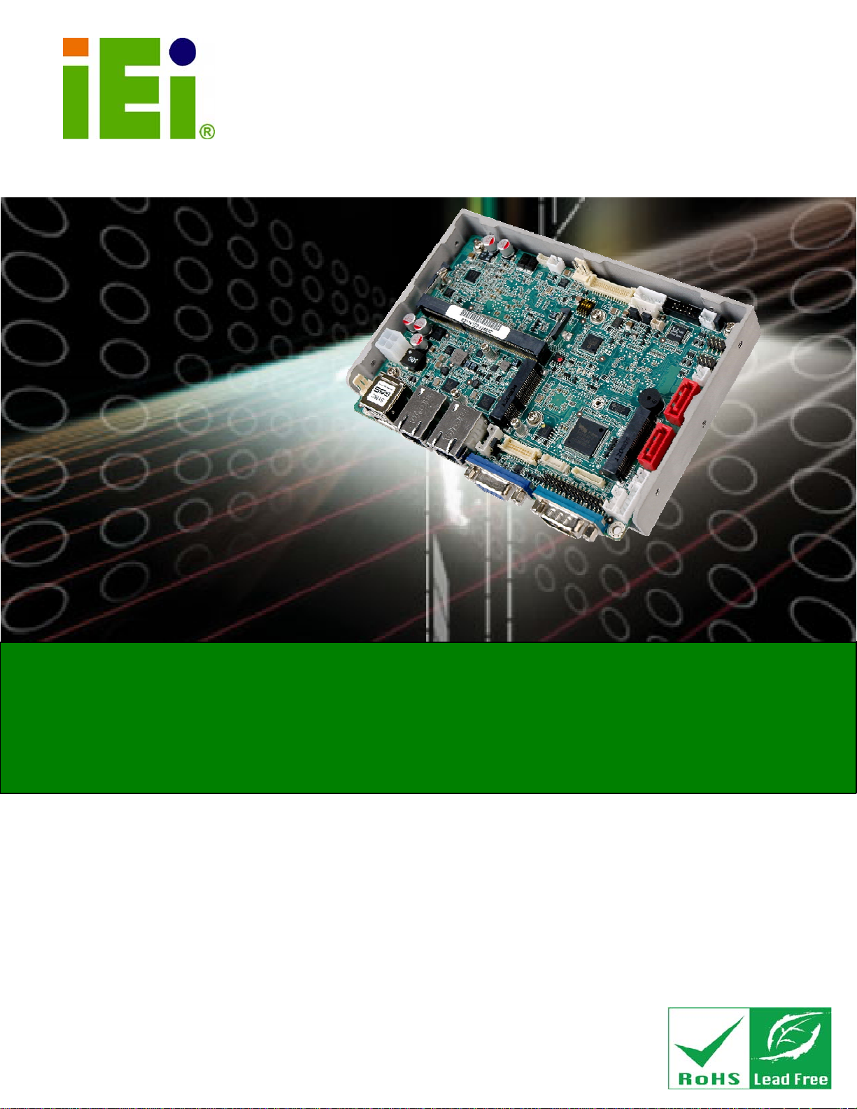
WAFER-CV-D25501/N26001 3.5" Motherboard
1
IEI Technology Corp.
MODEL:
WAFER-CV-D25501/N26001
3.5" SBC with Intel® Atom™ D2550/N2600 Processor,
DDR3, VGA/Dual LVDS, Dual PCIe GbE, USB 2.0,
PCIe Mini, SATA 3Gb/s, Audio and RoHS
User Manual
Rev. 1.03 – 11 December, 2012
Page i
Page 2
WAFER-CV-D25501/N26001 3.5" Motherboard
Revision
Date Version Changes
11 December, 2012
23 November, 2012
13 August, 2012
26 June, 20
1.03 Added CN6 connector information
1.02 Updated the note for the Intel® GMA driver limitation
1.01 Added a note for the Intel® GMA driver limitation
1.00 Initial release
Page ii
Page 3

WAFER-CV-D25501/N26001 3.5" Motherboard
COPYRIGHT NOTICE
The information in this document is subject to change without prior notice in order to
improve reliability, design and function and does not represent a commitment on the part
of the manufacturer.
In no event will the manufacturer be liable for direct, indirect, special, incidental, or
consequential damages arising out of the use or inability to use the product or
documentation, even if advised of the possibility of such damages.
This document contains proprietary information protected by copyright. All rights are
Copyright
reserved. No part of this manual may be reproduced by any mechanical, electronic, or
other means in any form without prior written permission of the manufacturer.
TRADEMARKS
All registered trademarks and product names mentioned herein are used for identification
purposes only and may be trademarks and/or registered trademarks of their respective
owners.
Page iii
Page 4

WAFER-CV-D25501/N26001 3.5" Motherboard
Table of Contents
1 INTRODUCTION.......................................................................................................... 1
1.1 INTRODUCTION........................................................................................................... 2
1.2 MODEL VARIATIONS ................................................................................................... 2
1.3 CONNECTORS ............................................................................................................. 3
1.4 DIMENSIONS............................................................................................................... 4
1.5 DATA FLOW................................................................................................................ 6
1.6 TECHNICAL SPECIFICATIONS ...................................................................................... 7
2 PACKING LIST.............................................................................................................9
2.1 ANTI-STATIC PRECAUTIONS ...................................................................................... 10
2.2 UNPACKING PRECAUTIONS....................................................................................... 10
2.3 PACKING LIST............................................................................................................11
2.4 OPTIONAL ITEMS...................................................................................................... 12
3 CONNECTORS ........................................................................................................... 13
3.1 PERIPHERAL INTERFACE CONNECTORS..................................................................... 14
3.1.1 W AFER-CV-D25501/N26001 Layout .............................................................. 14
3.1.2 Peripheral Interface Connectors ..................................................................... 15
3.1.3 External Interface Panel Connectors............................................................... 16
3.2 INTERNAL PERIPHERAL CONNECTORS ...................................................................... 16
3.2.1 5 V SATA Power Connectors............................................................................ 16
3.2.2 12 V Power Connector..................................................................................... 17
3.2.3 Audio Connector .............................................................................................. 17
3.2.4 Backlight Inverter Connectors......................................................................... 18
3.2.5 Battery Connector............................................................................................ 19
3.2.6 Digital Input/Output (DIO) Connector............................................................ 20
3.2.7 Fan Connectors................................................................................................ 21
3.2.8 Keyboard/Mouse Connector............................................................................ 22
3.2.9 LVDS1 Connector............................................................................................ 23
3.2.10 LVDS2 Connector.......................................................................................... 24
3.2.11 LVDS2 Backlight Control Connector............................................................. 26
Page iv
Page 5

WAFER-CV-D25501/N26001 3.5" Motherboard
3.2.12 PCIe Mini Card Slots..................................................................................... 26
3.2.13 Power & HDD LED Connector..................................................................... 28
3.2.14 Power Button Connector................................................................................ 29
3.2.15 Reset Button Connector ................................................................................. 30
3.2.16 RS-232 Serial Port Connectors...................................................................... 30
3.2.17 RS-422/485 Serial Port Connector................................................................ 31
3.2.18 SATA Drive Connectors ................................................................................. 32
3.2.19 USB Connectors............................................................................................. 33
3.3 EXTERNAL PERIPHERAL INTERFACE CONNECTOR PANEL ......................................... 34
3.3.1 Ethernet Connectors ........................................................................................ 34
3.3.2 Serial Port Connector (COM1) ....................................................................... 35
3.3.3 USB Connectors............................................................................................... 36
3.3.4 VGA Connector................................................................................................ 36
4 INSTALLATION ......................................................................................................... 38
4.1 ANTI-STATIC PRECAUTIONS ...................................................................................... 39
4.2 INSTALLATION CONSIDERATIONS.............................................................................. 39
4.3 SO-DIMM INSTALLATION ....................................................................................... 41
4.4 JUMPER SETTINGS .................................................................................................... 42
4.4.1 AT/ATX Power Selection Jumper.....................................................................42
4.4.2 Clear CMOS Jumper........................................................................................ 43
4.4.3 LVDS1 Voltage Selection.................................................................................. 44
4.4.4 LVDS2 Voltage Selection.................................................................................. 45
4.4.5 LVDS2 Panel Type Selection Jumper............................................................... 46
4.5 CHASSIS INSTALLATION............................................................................................ 47
4.5.1 Airflow.............................................................................................................. 47
4.5.2 Motherboard Installation................................................................................. 48
4.6 INTERNAL PERIPHERAL DEVICE CONNECTIONS........................................................48
4.6.1 Audio Kit Installation....................................................................................... 48
4.6.2 LVDS LCD Installation.................................................................................... 49
4.6.3 Full-size PCIe Mini Card Installation............................................................. 51
4.6.4 Half-size PCIe Mini Card Installation............................................................. 53
4.6.5 SATA Drive Connection ................................................................................... 54
4.6.6 Single RS-232 Cable........................................................................................ 55
4.6.7 Keyboard/Mouse Y-cable Connector ............................................................... 56
Page v
Page 6

4.7 EXTERNAL PERIPHERAL INTERFACE CONNECTION ................................................... 58
4.7.1 LAN Connection............................................................................................... 58
4.7.2 Serial Device Connection ................................................................................ 59
4.7.3 USB Connection (Dual Connector)................................................................. 60
4.7.4 VGA Monitor Connection ................................................................................ 60
4.8 HEAT SINK ENCLOSURE............................................................................................ 62
5 BIOS..............................................................................................................................64
5.1 INTRODUCTION......................................................................................................... 65
5.1.1 Starting Setup................................................................................................... 65
5.1.2 Using Setup...................................................................................................... 65
5.1.3 Getting Help..................................................................................................... 66
5.1.4 Unable to Reboot after Configuration Changes.............................................. 66
5.1.5 BIOS Menu Bar................................................................................................ 66
5.2 MAIN........................................................................................................................ 67
WAFER-CV-D25501/N26001 3.5" Motherboard
5.3 ADVANCED ............................................................................................................... 68
5.3.1 ACPI Settings................................................................................................... 68
5.3.2 RTC Wake Settings........................................................................................... 69
5.3.3 CPU Configuration.......................................................................................... 71
5.3.4 IDE Configuration........................................................................................... 72
5.3.5 USB Configuration........................................................................................... 73
5.3.6 F81866 Super IO Configuration...................................................................... 74
5.3.6.1 Serial Port n Configuration....................................................................... 74
5.3.7 F81866 H/W Monitor....................................................................................... 78
5.3.7.1 Smart Fan Mode Configuration................................................................ 79
5.3.8 Serial Port Console Redirection...................................................................... 80
5.3.9 iEi Feature....................................................................................................... 83
5.4 CHIPSET ................................................................................................................... 84
5.4.1 Host Bridge Configuration .............................................................................. 84
5.4.1.1 Intel IGD Configuration............................................................................ 85
5.4.2 South Bridge Configuration............................................................................. 87
5.5 BOOT........................................................................................................................ 88
5.6 SECURITY................................................................................................................. 90
5.7 EXIT......................................................................................................................... 90
6 SOFTWARE DRIVERS.............................................................................................. 92
Page vi
Page 7
WAFER-CV-D25501/N26001 3.5" Motherboard
6.1 AVAILABLE SOFTWARE DRIVERS .............................................................................. 93
6.2 ST ARTING THE DRIVER PROGRAM ............................................................................ 93
6.3 CHIPSET DRIVER INSTALLATION............................................................................... 95
6.4 GRAPHICS DRIVER INSTALLATION............................................................................ 99
6.5 LAN DRIVER INSTALLATION.................................................................................. 103
6.6 AUDIO DRIVER INSTALLATION ............................................................................... 105
A BIOS OPTIONS ........................................................................................................ 108
B ONE KEY RECOVERY............................................................................................111
B.1 ONE KEY RECOVERY INTRODUCTION .....................................................................112
B.1.1 System Requirement........................................................................................113
B.1.2 Supported Operating System..........................................................................114
B.2 SETUP PROCEDURE FOR WINDOWS.........................................................................115
B.2.1 Hardware and BIOS Setup .............................................................................116
B.2.2 Create Partitions............................................................................................116
B.2.3 Install Operating System, Drivers and Applications..................................... 120
B.2.4 Build-up Recovery Partition.......................................................................... 121
B.2.5 Create Factory Default Image....................................................................... 123
B.3 AUTO RECOVERY SETUP PROCEDURE.................................................................... 128
B.4 SETUP PROCEDURE FOR LINUX.............................................................................. 133
B.5 RECOVERY TOOL FUNCTIONS ................................................................................ 136
B.5.1 Factory Restore............................................................................................. 138
B.5.2 Backup System...............................................................................................139
B.5.3 Restore Your Last Backup.............................................................................. 140
B.5.4 Manual........................................................................................................... 141
B.6 RESTORE SYSTEMS FROM A LINUX SER VER THROUGH LAN.................................. 142
B.6.1 Configure DHCP Server Settings.................................................................. 143
B.6.2 Configure TFTP Settings ............................................................................... 144
B.6.3 Configure One Key Recovery Server Settings............................................... 145
B.6.4 Start the DHCP, TFTP and HTTP................................................................. 146
B.6.5 Create Shared Directory................................................................................ 146
B.6.6 Setup a Client System for Auto Recovery...................................................... 147
B.7 OTHER INFORMATION ............................................................................................ 150
B.7.1 Using AHCI Mode or ALi M5283 / VIA VT6421A Controller....................... 150
B.7.2 System Memory Requirement ........................................................................ 152
Page vii
Page 8

C TERMINOLOGY ..................................................................................................... 153
D DIGITAL I/O INTERFACE..................................................................................... 157
D.1 INTRODUCTION...................................................................................................... 158
D.2 DIO CONNECTOR PINOUTS ................................................................................... 158
D.3 ASSEMBLY LANGUAGE SAMPLES........................................................................... 159
D.3.1 Enable the DIO Input Function .................................................................... 159
D.3.2 Enable the DIO Output Function.................................................................. 159
E WA TCHDOG TIMER............................................................................................... 160
F HAZARDOUS MATERIALS DISCLOSURE ........................................................ 163
F.1 HAZARDOUS MATERIALS DISCLOSURE TABLE FOR IPB PRODUCTS CER TIFIED AS
ROHS COMPLIANT UNDER 2002/95/EC WITHOUT MERCURY ..................................... 164
WAFER-CV-D25501/N26001 3.5" Motherboard
Page viii
Page 9

WAFER-CV-D25501/N26001 3.5" Motherboard
List of Figures
Figure 1-1: WAFER-CV-D25501/N26001.......................................................................................2
Figure 1-2: Connectors ..................................................................................................................3
Figure 1-3: WAFER-CV-D25501/N26001 Dimensions (mm)........................................................4
Figure 1-4: External Interface Panel Dimensions (mm)..............................................................5
Figure 1-5: Data Flow Diagram......................................................................................................6
Figure 3-1: Connectors and Jumpers.........................................................................................14
Figure 3-2: 5 V SATA Power Connector Locations...................................................................16
Figure 3-3: 12 V Power Connector Location..............................................................................17
Figure 3-4: Audio Connector Location.......................................................................................18
Figure 3-5: Backlight Inverter Connector Locations.................................................................19
Figure 3-6: Battery Connector Location.....................................................................................20
Figure 3-7: Digital I/O Connector Location ................................................................................21
Figure 3-8: Fan Connector Locations.........................................................................................22
Figure 3-9: Keyboard/Mouse Connector Location....................................................................23
Figure 3-10: LVDS1 Connector Location ...................................................................................24
Figure 3-11: LVDS2 Connector Location ...................................................................................25
Figure 3-12: LVDS2 Backlight Control Connector Location....................................................26
Figure 3-13: PCIe Mini Card Slot Locations...............................................................................27
Figure 3-14: Power & HDD LED Connector Location................................................................28
Figure 3-15: Power Button Connector Location........................................................................29
Figure 3-16: Reset Button Connector Location.........................................................................30
Figure 3-17: RS-232 Serial Port Connector Locations..............................................................31
Figure 3-18: RS-422/485 Connector Location............................................................................32
Figure 3-19: SATA Drive Connector Locations.........................................................................32
Figure 3-20: USB Connector Locations......................................................................................33
Figure 3-21: External Peripheral Interface Connector..............................................................34
Figure 3-22: RJ-45 Ethernet Connector......................................................................................35
Figure 3-23: COM1 Pinout Locations..........................................................................................36
Figure 3-24: VGA Connector .......................................................................................................37
Figure 4-1: SO-DIMM Installation................................................................................................41
Page ix
Page 10

Figure 4-2: AT/ATX Power Selection Jumper Location............................................................43
Figure 4-3: Clear CMOS Jumper Location .................................................................................44
Figure 4-4: LVDS1 Voltage Selection Jumper Location ...........................................................45
Figure 4-5: LVDS2 Voltage Selection Jumper Location ...........................................................46
Figure 4-6: LVDS2 Panel Type Selection Switch Location.......................................................47
Figure 4-7: Audio Kit Cable Connection.....................................................................................49
Figure 4-8: LVDS Connector........................................................................................................50
Figure 4-9: Backlight Inverter Connection.................................................................................51
Figure 4-10: Remove the Retention Screw for the Full-size PCIe Mini Card..........................52
Figure 4-11: Insert the Full-size PCIe Mini Card into the Socket at an Angle.........................52
Figure 4-12: Secure the Full-size PCIe Mini Card......................................................................53
Figure 4-13: Remove the Retention Screws for the Half-size PCIe Mini Card........................53
Figure 4-14: Insert the Half-size PCIe Mini Card into the Socket at an Angle........................54
Figure 4-15: Secure the Half-size PCIe Mini Card .....................................................................54
WAFER-CV-D25501/N26001 3.5" Motherboard
Figure 4-16: SATA Drive Cable Connection...............................................................................55
Figure 4-17: Single RS-232 Cable Installation ...........................................................................56
Figure 4-18: Keyboard/mouse Y-cable Connection..................................................................57
Figure 4-19: LAN Connection......................................................................................................58
Figure 4-20: Serial Device Connector.........................................................................................59
Figure 4-21: USB Connector........................................................................................................60
Figure 4-22: VGA Connector .......................................................................................................61
Figure 4-23: Heat Sink Retention Screws ..................................................................................63
Figure 6-1: Start Up Screen .........................................................................................................94
Figure 6-2: Drivers........................................................................................................................94
Figure 6-3: Chipset Driver Screen...............................................................................................95
Figure 6-4: Chipset Driver Welcome Screen..............................................................................96
Figure 6-5: Chipset Driver License Agreement.........................................................................97
Figure 6-6: Chipset Driver Read Me File ....................................................................................97
Figure 6-7: Chipset Driver Setup Operations ............................................................................98
Figure 6-8: Chipset Driver Installation Finish Screen...............................................................99
Figure 6-9: Graphics Driver Welcome Screen........................................................................ 100
Figure 6-10: Graphics Driver License Agreement.................................................................. 101
Figure 6-11: Graphics Driver Read Me File............................................................................. 101
Figure 6-12: Graphics Driver Setup Operations..................................................................... 102
Figure 6-13: Graphics Driver Installation Finish Screen ....................................................... 102
Page x
Page 11

WAFER-CV-D25501/N26001 3.5" Motherboard
Figure 6-14: LAN Driver Welcome Screen .............................................................................. 103
Figure 6-15: LAN Driver Installation ........................................................................................ 104
Figure 6-16: LAN Driver Installation Complete....................................................................... 104
Figure 6-17: Audio Driver Installation File Extraction............................................................ 105
Figure 6-18: Audio Driver Welcome Screen............................................................................ 106
Figure 6-19: Audio Driver Installation...................................................................................... 106
Figure 6-20: Audio Driver Installation Complete.................................................................... 107
Figure B-1: IEI One Key Recovery Tool Menu........................................................................ 112
Figure B-2: Launching the Recovery Tool.............................................................................. 117
Figure B-3: Recovery Tool Setup Menu .................................................................................. 117
Figure B-4: Command Prompt ................................................................................................. 118
Figure B-5: Partition Creation Commands.............................................................................. 119
Figure B-6: Launching the Recovery Tool.............................................................................. 121
Figure B-7: Manual Recovery Environment for Windows..................................................... 121
Figure B-8: Building the Recovery Partition........................................................................... 122
Figure B-9: Press Any Key to Continue.................................................................................. 122
Figure B-10: Press F3 to Boot into Recovery Mode............................................................... 123
Figure B-11: Recovery Tool Menu ........................................................................................... 123
Figure B-12: About Symantec Ghost Window........................................................................ 124
Figure B-13: Symantec Ghost Path ......................................................................................... 124
Figure B-14: Select a Local Source Drive ............................................................................... 125
Figure B-15: Select a Source Partition from Basic Drive ...................................................... 125
Figure B-16: File Name to Copy Image to ............................................................................... 126
Figure B-17: Compress Image.................................................................................................. 126
Figure B-18: Image Creation Confirmation............................................................................. 127
Figure B-19: Image Creation Complete................................................................................... 127
Figure B-20: Image Creation Complete................................................................................... 127
Figure B-21: Press Any Key to Continue................................................................................ 128
Figure B-22: Auto Recovery Utility.......................................................................................... 129
Figure B-23: Disable Automatically Restart............................................................................ 129
Figure B-24: Launching the Recovery Tool............................................................................ 130
Figure B-25: Auto Recovery Environment for Windows ....................................................... 130
Figure B-26: Building the Auto Recovery Partition................................................................ 131
Figure B-27: Factory Default Image Confirmation ................................................................. 131
Figure B-28: Image Creation Complete................................................................................... 132
Page xi
Page 12

Figure B-29: Press any key to continue.................................................................................. 132
Figure B-30: IEI Feature ............................................................................................................ 133
Figure B-31: Partitions for Linux.............................................................................................. 134
Figure B-32: System Configuration for Linux......................................................................... 135
Figure B-33: Access menu.lst in Linux (Text Mode).............................................................. 135
Figure B-34: Recovery Tool Menu ........................................................................................... 136
Figure B-35: Recovery Tool Main Menu.................................................................................. 137
Figure B-36: Restore Factory Default...................................................................................... 138
Figure B-37: Recovery Complete Window.............................................................................. 138
Figure B-38: Backup System.................................................................................................... 139
Figure B-39: System Backup Complete Window ................................................................... 139
Figure B-40: Restore Backup................................................................................................... 140
Figure B-41: Restore System Backup Complete Window..................................................... 140
Figure B-42: Symantec Ghost Window ................................................................................... 141
WAFER-CV-D25501/N26001 3.5" Motherboard
Figure B-43: Disable Automatically Restart............................................................................ 148
Page xii
Page 13
WAFER-CV-D25501/N26001 3.5" Motherboard
List of Tables
Table 1-1: WAFER-CV-D25501/N26001 Model Variations...........................................................2
Table 1-2: WAFER-CV-D25501/N26001 Specifications ...............................................................8
Table 2-1: Packing List.................................................................................................................12
Table 2-2: Optional Items.............................................................................................................12
Table 3-1: Peripheral Interface Connectors...............................................................................15
Table 3-2: Rear Panel Connectors..............................................................................................16
Table 3-3: 5 V SATA Power Connector Pinouts ........................................................................17
Table 3-4: 12 V Power Connector Pinouts .................................................................................17
Table 3-5: Audio Connector Pinouts ..........................................................................................18
Table 3-6: Backlight Inverter Connector Pinouts......................................................................19
Table 3-7: Battery Connector Pinouts........................................................................................20
Table 3-8: Digital I/O Connector Pinouts....................................................................................21
Table 3-9: Fan Connector Pinouts..............................................................................................22
Table 3-10: Keyboard/Mouse Connector Pinouts .....................................................................23
Table 3-11: LVDS1 Connector Pinouts.......................................................................................24
Table 3-12: LVDS2 Connector Pinouts.......................................................................................25
Table 3-13: LVDS2 Backlight Control Connector Pinouts........................................................26
Table 3-14: PCIe Mini Card Slot Pinouts ....................................................................................28
Table 3-15: Power & HDD LED Connector Pinouts...................................................................29
Table 3-16: Power Button Connector Pinouts...........................................................................29
Table 3-17: Reset Button Connector Pinouts............................................................................30
Table 3-18: RS-232 Serial Port Connector Pinouts...................................................................31
Table 3-19: RS-422/485Connector Pinouts................................................................................32
Table 3-20: SATA Drive Connector Pinouts...............................................................................33
Table 3-21: USB Connector Pinouts...........................................................................................34
Table 3-22: LAN Pinouts ..............................................................................................................34
Table 3-23: RJ-45 Ethernet Connector LEDs.............................................................................35
Table 3-24: RS-232 Serial Port (COM 1) Pinouts .......................................................................35
Table 3-25: USB Port Pinouts......................................................................................................36
Table 3-26: VGA Connector Pinouts...........................................................................................37
Page xiii
Page 14

Table 4-1: Jumpers.......................................................................................................................42
Table 4-2: AT/ATX Power Selection Jumper Settings...............................................................43
Table 4-3: Clear CMOS Jumper Settings....................................................................................43
Table 4-4: LVDS1 Voltage Selection Jumper Settings..............................................................44
Table 4-5: LVDS2 Voltage Selection Jumper Settings..............................................................45
Table 4-6: LVDS2 Panel Resolution............................................................................................47
Table 5-1: BIOS Navigation Keys................................................................................................66
WAFER-CV-D25501/N26001 3.5" Motherboard
Page xiv
Page 15

WAFER-CV-D25501/N26001 3.5" Motherboard
BIOS Menus
BIOS Menu 1: Main.......................................................................................................................67
BIOS Menu 2: Advanced..............................................................................................................68
BIOS Menu 3: ACPI Settings .......................................................................................................69
BIOS Menu 4: RTC Wake Settings..............................................................................................70
BIOS Menu 5: CPU Configuration...............................................................................................71
BIOS Menu 6: IDE Configuration.................................................................................................72
BIOS Menu 7: USB Configuration...............................................................................................73
BIOS Menu 8: Super IO Configuration........................................................................................74
BIOS Menu 9: Serial Port n Configuration Menu.......................................................................74
BIOS Menu 10: F81866 H/W Monitor...........................................................................................78
BIOS Menu 11: Smart Fan Mode Configuration ........................................................................80
BIOS Menu 12: Serial Port Console Redirection.......................................................................81
BIOS Menu 13: IEI Feature...........................................................................................................83
BIOS Menu 14: Chipset................................................................................................................84
BIOS Menu 15: Host Bridge Configuration................................................................................ 85
BIOS Menu 16: Intel IGD Configuration......................................................................................85
BIOS Menu 17: Southbridge Chipset Configuration.................................................................87
BIOS Menu 18: Boot.....................................................................................................................88
BIOS Menu 19: Security...............................................................................................................90
BIOS Menu 20:Exit........................................................................................................................91
WAFER-CV-D25501/N26001
Page xv
Page 16
WAFER-CV-D25501/N26001 3.5" Motherboard
1 Introduction
Chapter
1
Page 1
Page 17
1.1 Introduction
Figure 1-1: WAFER-CV-D25501/N26001
WAFER-CV-D25501/N26001 3.5" Motherboard
The WAFER-CV-D25501/N26001 3.5” motherboard is an Intel® Atom™ D2550/N2600
processor platform that supports one 1066 MHz or 800 MHz DDR3 SO-DIMM memory.
The WAFER-CV-D25501/N26001 supports VGA display output and comes with two LVDS
connectors supporting 24-bit or 18-bit LVDS screens. Maximum six USB ports, two SATA
3Gb/s connectors, two PCIe Mini card slots, four COM ports, and one audio connector
provide flexible expansion options.
1.2 Model Variations
The model variations of the WAFER-CV-D25501/N26001 are listed below.
Model No. CPU
WAFER-CV-D25501-R10
WAFER-CV-N26001-R10
Table 1-1: WAFER-CV-D25501/N26001 Model Variations
Intel® Atom D2550 1.86 GHz
Intel® Atom N2600 1.6 GHz
Page 2
Page 18
WAFER-CV-D25501/N26001 3.5" Motherboard
1.3 Connectors
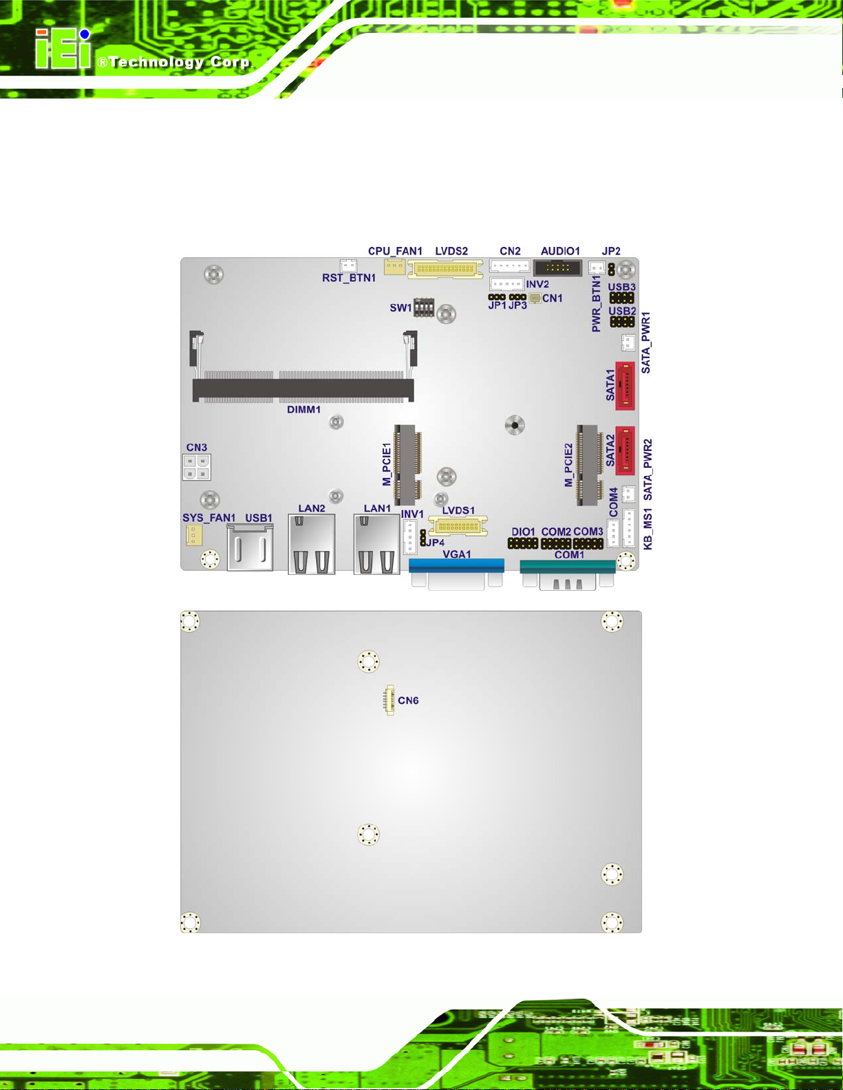
The connectors on the WAFER-CV-D25501/N26001 are shown in the figure bel ow.
Figure 1-2: Connectors
Page 3
Page 19
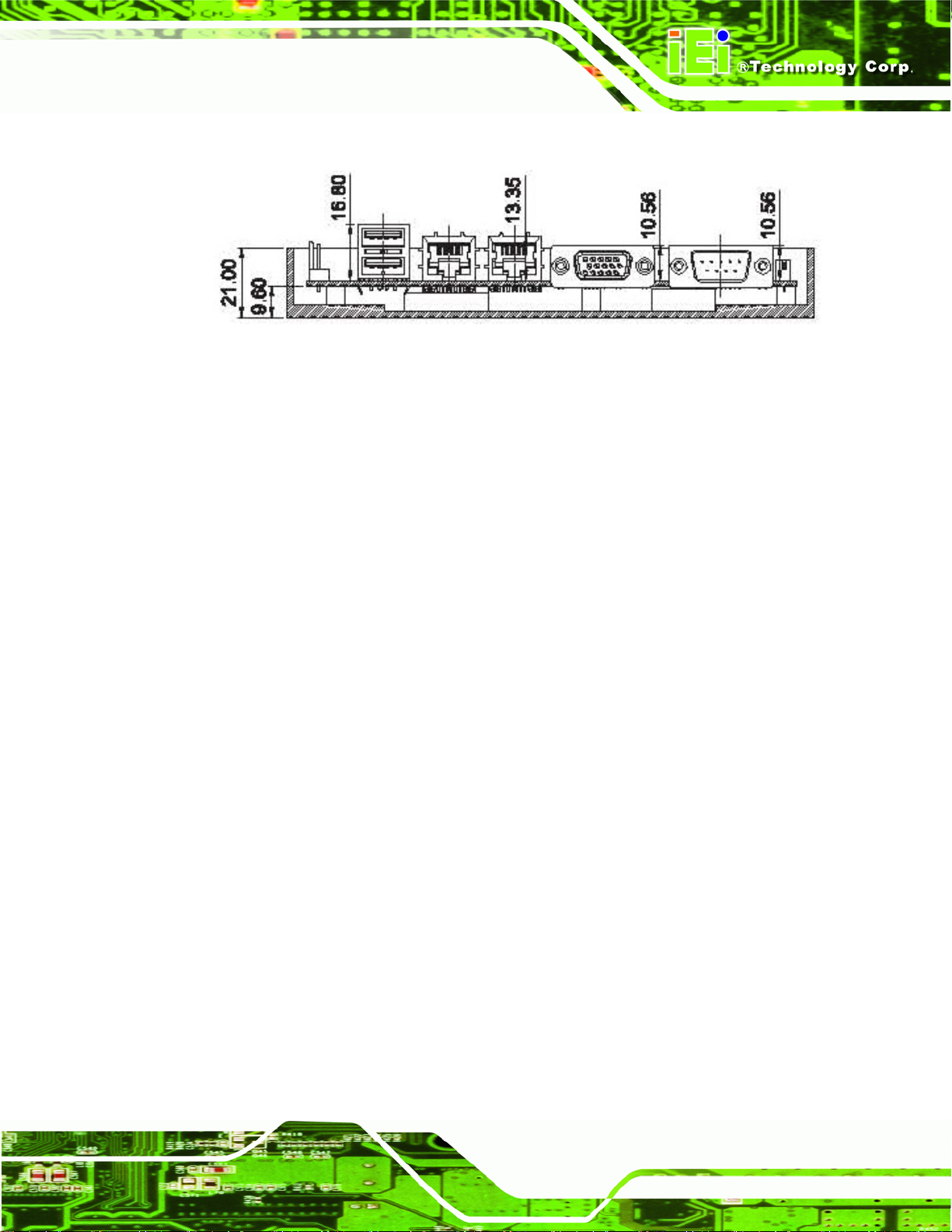
1.4 Dimensions
The main dimensions of the WAFER-CV-D25501/N26001 are shown in the diagram
below.
WAFER-CV-D25501/N26001 3.5" Motherboard
Page 4
Figure 1-3: WAFER-CV-D25501/N26001 Dimensions (mm)
Page 20
WAFER-CV-D25501/N26001 3.5" Motherboard
.
Figure 1-4: External Interface Panel Dimensions (mm)
Page 5
Page 21
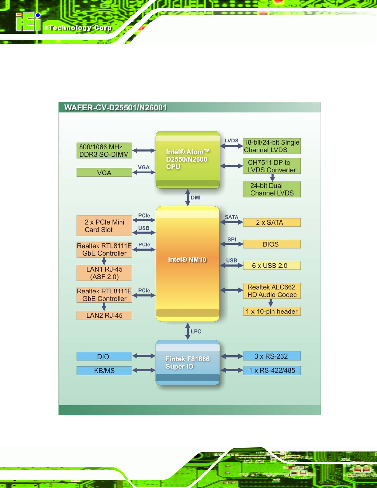
1.5 Data Flow
6Figure 1-5 shows the data flow between the system chipset, the CPU and other
components installed on the motherboard.
WAFER-CV-D25501/N26001 3.5" Motherboard
Figure 1-5: Data Flow Diagram
Page 6
Page 22
WAFER-CV-D25501/N26001 3.5" Motherboard
1.6 Technical Specifications
The WAFER-CV-D25501/N26001 technical specifications are listed below.
Specification/Model WAFER-CV-D25501 WAFER-CV-N26001
Form Factor
System CPU
System Chipset
Memory
Graphics Engine
Display
3.5”
Intel® Atom™ D2550 1.86 GHz Intel® Atom™ N2600 1.6 GHz
Intel® NM10
One 1066 MHz DDR3/DDR3L (1.35V)
SO-DIMM support (up to 4 GB)
Intel® GMA 3650 with a 640 MHz
graphics core
Dual display supported
One VGA
One LVDS1 is integrated in the Intel® Atom™ D2550/N2600 processor
One LVDS2 is driven by the Chrontel CH7511 DP to LVDS converter
24-bit single-channel LVDS1 with
up to 1440x900 resolution
24-bit dual-channel LVDS2 with up
to 1920x1200 resolution
One 800 MHz DDR3/DDR3L (1.35V)
SO-DIMM support (up to 2 GB)
Intel® GMA 3600 with a 400 MHz
graphics core
18-bit single-channel LVDS1 with
up to 1366x768 resolution
24-bit dual-channel LVDS2 with up
to 1600x1200 resolution
Ethernet
BIOS
Super I/O Controller
Watchdog Timer
Expansion
Audio
COM
Digital I/O
Dual Realtek RTL8111E PCIe GbE cont roller (LAN1 with ASF 2.0
support)
UEFI BIOS
Fintek F81866
Software programmable supports 1~2 55 sec. system reset
One full-size PCIe Mini card slot with mSATA support
One half-size PCIe Mini card slot
Realtek ALC662 HD Audio codec
Three RS-232 (one by external connector; two by on-board pin headers)
One RS-422/485 by internal 4-pin wafer connector
One 8-bit digital input/output connector (4-bit input/4-bit output)
Page 7
Page 23
Specification/Model WAFER-CV-D25501 WAFER-CV-N26001
WAFER-CV-D25501/N26001 3.5" Motherboard
Fan
Keyboard/mouse
SATA
USB
Power Supply
Power Consumption
Operating
Temperature
One 3-pin CPU fan connector
One 3-pin system fan connector
One internal pin-header connector
Two SATA 3Gb/s ports with 5V power
Six USB 2.0/1.1 devices supported:
Two by external connectors
Four by on-board pin headers
12 V only
AT and ATX support
One internal 4-pin (2x2) power connector
12V @ 1.53 A (1.86 GHz Intel®
Atom™ D2550 with 1 GB 1066 MHz
DDR3 SO-DIMM memory)
-20ºC ~ 60ºC with free air
-20ºC ~ 70ºC with force air
12V @ 1.15 A (1.6 GHz Intel®
Atom™ N2600 with 1 GB 1066 MHz
DDR3 SO-DIMM memory)
-20ºC ~ 70ºC with free air
-20ºC ~ 75ºC with force air
Storage
Temperature
Humidity (Operating)
Dimensions (LxW)
Weight (GW/NW)
Table 1-2: WAFER-CV-D25501/N26001 Specifications
-30ºC ~ 80ºC -30ºC ~ 85ºC
5% ~ 95% (non-condensing)
146 mm x 102 mm
600 g/250 g
Page 8
Page 24

WAFER-CV-D25501/N26001 3.5" Motherboard
2 Packing List
Chapter
2
Page 9
Page 25
WAFER-CV-D25501/N26001 3.5" Motherboard
2.1 Anti-static Precautions
WARNING!
Static electricity can destroy certain electronics. Make sure to follow the
ESD precautions to prevent damage to the product, and injury to the
user.
Make sure to adhere to the following guidelines:
Wear an anti-static wristband: Wearing an anti-static wristband can prevent
electrostatic discharge.
Self-grounding: Touch a grounded conductor every few minutes to discharge
any excess static buildup.
Use an anti-static pad: When configuring any circuit board, place it on an
anti-static mat.
Only handle the edges of the PCB: Don't touch the surface of the
motherboard. Hold the motherboard by the edges when handling.
2.2 Unpacking Precautions
When the WAFER-CV-D25501/N26001 is unpacked, please do the following:
Follow the antistatic guidelines above.
Make sure the packing box is facing upwards when opening.
Make sure all the packing list items are present.
Page 10
Page 26
WAFER-CV-D25501/N26001 3.5" Motherboard
2.3 Packing List
NOTE:
If any of the components listed in the checklist below are missing, do
not proceed with the installation. Contact the IEI reseller or vendor the
WAFER-CV-D25501/N26001 was purchased from or contact an IEI
sales representative directly by sending an email to 33sales@iei.com.tw.
The WAFER-CV-D25501/N26001 is shipped with the following components:
Quantity Item and Part Number Image
1 WAFER-CV-D25501/N26001 motherboard
1 SATA and power cable
(P/N: 32801-000201-100-RS)
1 Audio cable
(P/N: 32000-072100-RS)
1 RS-232 cable
(P/N: 32205-002700-100-RS)
1 KB/MS cable
(P/N: 32000-023800-RS)
1 Power cable
(P/N: 32100-087100-RS)
Page 11
Page 27
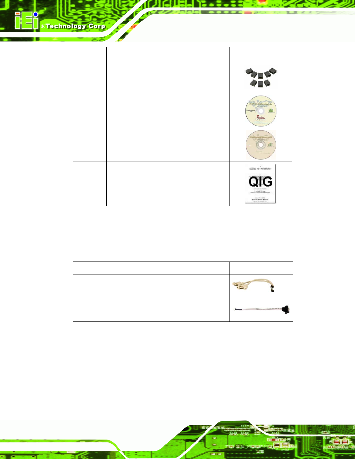
Quantity Item and Part Number Image
1 Mini jumper pack
1 One Key Recovery CD
1 Utility CD
1 Quick Installation Guide
WAFER-CV-D25501/N26001 3.5" Motherboard
Table 2-1: Packing List
2.4 Optional Items
The following are optional components which may be separately purchased:
Item and Part Number Image
Dual USB cable (wo bracket)
(P/N: 32001-008600-100-RS)
RS-422/485 cable (200 mm)
(P/N: 32205-003800-100-RS)
Table 2-2: Optional Items
Page 12
Page 28
WAFER-CV-D25501/N26001 3.5" Motherboard
3 Connectors
Chapter
3
Page 13
Page 29
WAFER-CV-D25501/N26001 3.5" Motherboard
3.1 Peripheral Interface Connectors
This chapter details all the jumpers and connectors.
3.1.1 WAFER-CV-D25501/N26001 Layout
The figure below shows all the connectors and jumpers.
Figure 3-1: Connectors and Jumpers
Page 14
Page 30
WAFER-CV-D25501/N26001 3.5" Motherboard
3.1.2 Peripheral Interface Connectors
The table below lists all the connectors on the board.
Connector Type Label
5 V SATA power connectors 2-pin wafer SATA_PWR1,
SATA_PWR2
12 V power connector 4-pin Molex power
connector
Audio connector 10-pin box header AUDIO1
Backlight inverter connectors 5-pin wafer INV1, INV2
Battery connector 2-pin wafer CN1
Digital Input/Output (DIO) connector 10-pin header DIO1
Fan connectors 3-pin wafer CPU_FAN1,
Keyboard and mouse connector 6-pin wafer KB_MS1
LVDS connectors 20-pin/30-pin crimp LVDS1, LVDS2
LVDS2 backlight control connector 6-pin wafer CN6
PCIe Mini card slots 52-pin PCIe Mini M_PCIE1,
Power & HDD LED connector 6-pin header CN2
CN3
SYS_FAN2
M_PCIE2
Power button connector 2-pin wafer PWR_BTN1
Reset button connector 2-pin wafer RST_BTN1
RS-232 serial port connectors 10-pin header COM2, COM3
RS-422/485 serial port connector 4-pin wafer COM4
Serial ATA (SATA) drive connectors 7-pin SATA SATA1, SATA2
USB 2.0 connectors 8-pin header USB2, USB3
Table 3-1: Peripheral Interface Connectors
Page 15
Page 31

WAFER-CV-D25501/N26001 3.5" Motherboard
3.1.3 External Interface Panel Connectors
The table below lists the connectors on the external I/O panel.
Connector Type Label
Dual USB port Dual USB port USB1
Ethernet connectors RJ-45 LAN1, LAN2
RS-232 serial port connector Male DB-9 COM1
VGA connector 15-pin female VGA1
Table 3-2: Rear Panel Connectors
3.2 Internal Peripheral Connectors
The section describes all of the connectors on the WAFER-CV-D25501/N26001.
3.2.1 5 V SATA Power Connectors
CN Label: SATA_PWR1, SATA_PWR2
CN Type:
CN Location:
CN Pinouts:
Use the 5 V SATA power connectors to connect to SATA device power connection.
2-pin wafer
See Figure 3-2
See Table 3-3
Page 16
Figure 3-2: 5 V SATA Power Connector Locations
Page 32

WAFER-CV-D25501/N26001 3.5" Motherboard
Pin No. Description
1 +5V
2 Ground
Table 3-3: 5 V SATA Power Connector Pinouts
3.2.2 12 V Power Connector
CN Label: CN3
CN Type:
CN Location:
CN Pinouts:
4-pin Molex power connector
Figure 3-3
See
Table 3-4
See
The ATX power connector connects to an ATX power supply.
Figure 3-3: 12 V Power Connector Location
Pin Description
1 GND
2 GND
3 +12V
4 +12V
Table 3-4: 12 V Power Connector Pinouts
3.2.3 Audio Connector
CN Label: AUDIO1
CN Type:
CN Location:
CN Pinouts:
10-pin box header
Figure 3-4
See
Table 3-5
See
Page 17
Page 33

WAFER-CV-D25501/N26001 3.5" Motherboard
The 10-pin audio connector is connected to external audio devices including speakers a nd
microphones for the input and output of audio signals to and from the system.
Figure 3-4: Audio Connector Location
Pin Description Pin Description
1
3
5
7
9
Line-out_R
AUD_GND
Line-out _L
AUD_GND
MIC1_R
2
4
6
8
10
Line-in_R
AUD_GND
Line-in _L
AUD_GND
MIC1_L
Table 3-5: Audio Connector Pinouts
3.2.4 Backlight Inverter Connectors
CN Label:
CN Type:
CN Location:
CN Pinouts:
The backlight inverter connectors provide the backlights on the LCD display connected to
the WAFER-CV-D25501/N26001 with +12V of power.
INV1, INV2
5-pin wafer
Figure 3-5
See
Table 3-6
See
Page 18
Page 34

WAFER-CV-D25501/N26001 3.5" Motherboard
Figure 3-5: Backlight Inverter Connector Locations
Pin Description
1
2
3
4
5
LCD_BKLTCTL
GROUND
+12V
GROUND
LCD_BKLEN
Table 3-6: Backlight Inverter Connector Pinouts
3.2.5 Battery Connector
CAUTION:
Risk of explosion if battery is replaced by an incorrect type. Only
certified engineers should replace the on-board battery.
Dispose of used batteries according to instructions and local
regulations.
CN Label: CN1
CN Type:
2-pin wafer
Page 19
Page 35

CN Location:
CN Pinouts:
This is connected to the system battery. The battery provides power to the system clock to
retain the time when power is turned off.
See
See
WAFER-CV-D25501/N26001 3.5" Motherboard
Figure 3-6
Table 3-7
Figure 3-6: Battery Connector Location
Pin Description
1 Battery+
2 GND
Table 3-7: Battery Connector Pinouts
3.2.6 Digital Input/Output (DIO) Connector
CN Label: DIO1
CN Type:
CN Location:
CN Pinouts:
The digital input/output connector is managed through a Super I/O chip. The DIO
connector pins are user programmable.
10-pin header
See Figure 3-7
See Table 3-8
Page 20
Page 36

WAFER-CV-D25501/N26001 3.5" Motherboard
Figure 3-7: Digital I/O Connector Location
Pin Description Pin Description
1 GND 2 VCC
3 Output 3 4 Output 2
5 Output 1 6 Output 0
7 Input 3 8 Input 2
9 Input 1 10 Input 0
Table 3-8: Digital I/O Connector Pinouts
3.2.7 Fan Connectors
CN Label: CPU_FAN1, SYS_FAN1
CN Type:
CN Location:
CN Pinouts:
The fan connectors attach to the CPU/system cooling fans.
3-pin wafer
See Figure 3-8
See Table 3-9
Page 21
Page 37

Figure 3-8: Fan Connector Locations
WAFER-CV-D25501/N26001 3.5" Motherboard
PIN NO. DESCRIPTION
1 GND
2 +12 V
3 Fan Speed Detect
Table 3-9: Fan Connector Pinouts
3.2.8 Keyboard/Mouse Connector
CN Label: KB_MS1
CN Type:
CN Location:
CN Pinouts:
The keyboard and mouse connector can be connected to a standard PS/2 cable or PS/2
Y-cable to add keyboard and mouse functionality to the system.
6-pin wafer
Figure 3-9
See
Table 3-10
See
Page 22
Page 38

WAFER-CV-D25501/N26001 3.5" Motherboard
Figure 3-9: Keyboard/Mouse Connector Location
Pin Description
1 +5 V KB DATA
2 MS DATA
3 MS CLK
4 KB DATA
5 KB CLK
6 GROUND
Table 3-10: Keyboard/Mouse Connector Pinouts
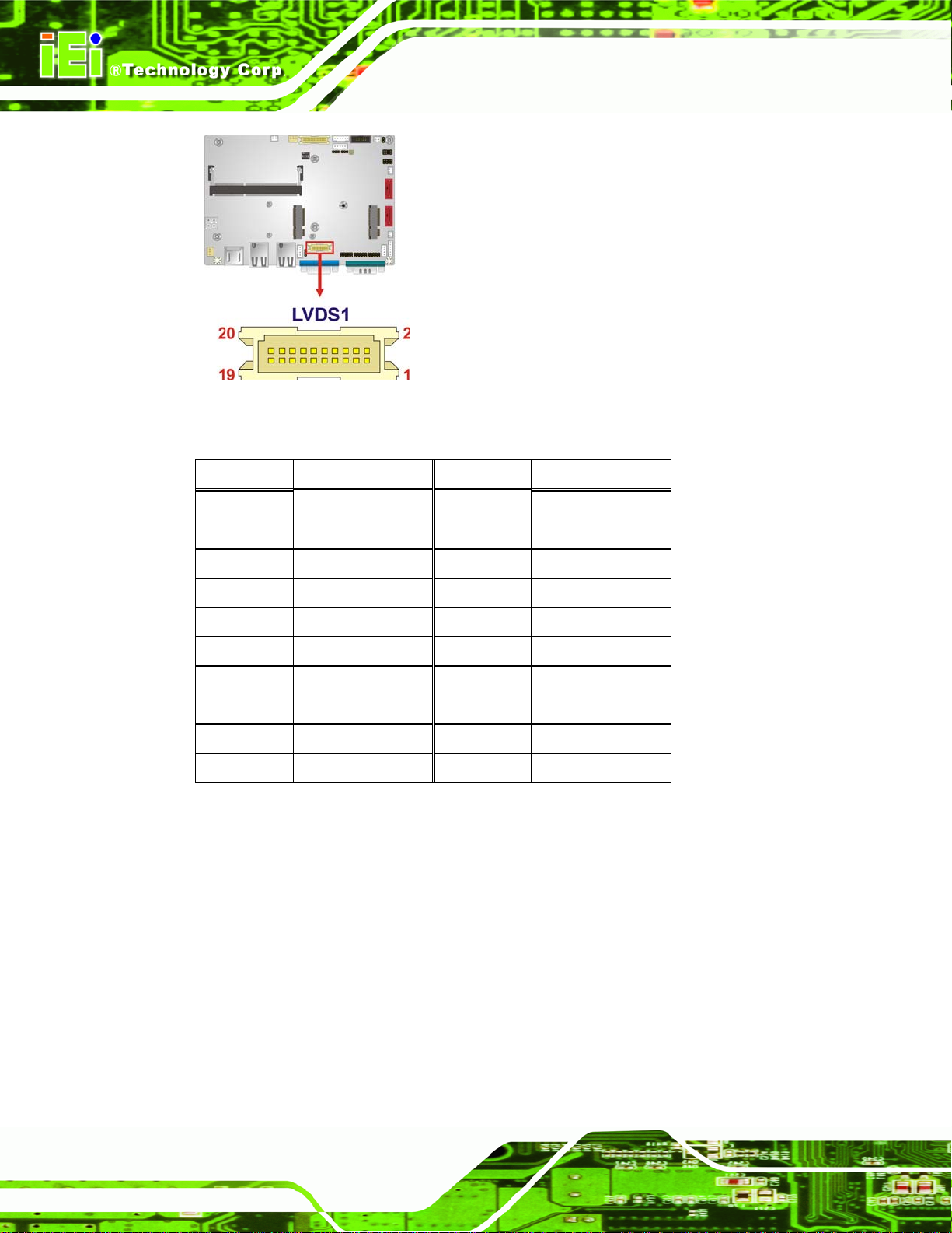
3.2.9 LVDS1 Connector
CN Label: LVDS1
CN Type:
CN Location:
CN Pinouts:
The 20-pin LVDS LCD connector can be connected to an 18-bit/24-bit single-channel
LVDS panel.
20-pin crimp
Figure 3-10
See
Table 3-11
See
Page 23
Page 39
WAFER-CV-D25501/N26001 3.5" Motherboard
Figure 3-10: LVDS1 Connector Location
Pin Description Pin Description
1 GND 2 GND
3 LVDS_DATA0 4 LVDS_DATA0#
5 LVDS_DATA1 6 LVDS_DATA1#
7 LVDS_DATA2 8 LVDS_DATA2#
9 LVDS_CLK 10 LVDS_CLK#
11 LVDS_DATA3 12 LVDS_DATA3#
13 GND 14 GND
15 LDDC_DATA 16 LDDC_CLK
17 VCC_LCD 18 VCC_LCD
19 VCC_LCD 20 VCC_LCD
Table 3-11: LVDS1 Connector Pinouts
3.2.10 LVDS2 Connector
CN Label: LVDS2
CN Type:
CN Location:
30-pin crimp
See
Figure 3-11
Page 24
Table 3-12
CN Pinouts:
See
The 30-pin LVDS LCD connector can be connected to a 24-bit dual-chann el LVDS panel.
Page 40

WAFER-CV-D25501/N26001 3.5" Motherboard
Figure 3-11: LVDS2 Connector Location
Pin Description Pin Description
1 GND 2 GND
3 LVDS_DATA0 4 LVDS_DATA0#
5 LVDS_DATA1 6 LVDS_DATA1#
7 LVDS_DATA2 8 LVDS_DATA2#
9 LVDS_CLK1 10 LVDS_CLK1#
11 LVDS_DATA3 12 LVDS_DATA3#
13 GND 14 GND
15 LVDS_DATA4 16 LVDS_DATA4#
17 LVDS_DATA5 18 LVDS_DATA5#
19 LVDS_DATA6 20 LVDS_DATA6#
21 LVDS_CLK2 22 LVDS_CLK2#
23 LVDS_DATA7 24 LVDS_DATA7#
25 GND 26 GND
27 VCC_LCD 28 VCC_LCD
29 VCC_LCD 30 VCC_LCD
Table 3-12: LVDS2 Connector Pinouts
Page 25
Page 41

WAFER-CV-D25501/N26001 3.5" Motherboard
3.2.11 LVDS2 Backlight Control Connector
CN Label: CN6
CN Type:
CN Location:
CN Pinouts:
6-pin wafer
Figure 3-12
See
Table 3-13
See
This connector allows control of the LVDS2 panel backlight.
Figure 3-12: LVDS2 Backlight Control Connector Location
Function Pin Description
Panel power button
1 PWRDN
2 GND
Panel brightness +
Panel brightness -
3 BLUP
4 GND
5 BLDN
6 GND
Table 3-13: LVDS2 Backlight Control Connector Pinouts
3.2.12 PCIe Mini Card Slots
CN Label: M_PCIE1, M_PCIE2
CN Type:
CN Location:
CN Pinouts:
The M_PCIE2 slot can be connected to a full-size PCIe Mini card while the M_PCIE1 slot
can be connected to a half-size PCIe Mini card.
52-pin PCIe Mini card slot
Figure 3-13
See
Table 3-14
See
Page 26
Page 42

WAFER-CV-D25501/N26001 3.5" Motherboard
NOTE:
The M_PCIE2 slot supports mSATA devices.
Figure 3-13: PCIe Mini Card Slot Locations
Pin Description Pin Description
1 PCIE_WAKE# 2 VCC3
3 N/C 4 GND
5 N/C 6 1.5V
7 N/C 8 N/C
9 GND 10 N/C
11 PCIE_CLK# 12 N/C
13 PCIE_CLK 14 N/C
15 GND 16 N/C
17 N/C 18 GND
19 N/C 20 N/C
21 GND 22 PCIRST#
23 PCIE_RXN 24 VCC3
25 PCIE_RXP 26 GND
27 GND 28 1.5V
29 GND 30 SMBCLK
31 PCIE_TXN 32 SMBDATA
33 PCIE_TXP 34 GND
35 GND 36 USBD-
Page 27
Page 43

Pin Description Pin Description
37 GND 38 USBD+
39 VCC3 40 GND
41 VCC3 42 N/C
43 GND 44 N/C
45 N/C 46 N/C
47 N/C 48 1.5V
49 N/C 50 GND
51 N/C 52 VCC3
WAFER-CV-D25501/N26001 3.5" Motherboard
Table 3-14: PCIe Mini Card Slot Pinouts
3.2.13 Power & HDD LED Connector
CN Label: CN2
CN Type:
CN Location:
CN Pinouts:
6-pin wafer
Figure 3-14
See
Table 3-15
See
The LED connector connects to an HDD indicator LED and a power LED on the system
chassis to inform the user about HDD activity and the power on/off status of the system.
Page 28
Figure 3-14: Power & HDD LED Connector Location
Page 44

WAFER-CV-D25501/N26001 3.5" Motherboard
Pin Description
1 +5V
2 GND
3 Power LED+
4 Power LED5 HDD LED+
6 HDD LED-
Table 3-15: Power & HDD LED Connector Pinouts
3.2.14 Power Button Connector
CN Label: PWR_BTN1
CN Type:
CN Location:
CN Pinouts:
2-pin wafer
Figure 3-15
See
Table 3-16
See
The power button connector is connected to a power switch on the system chassis to
enable users to turn the system on and off.
Figure 3-15: Power Button Connector Location
Pin Description
1
2
PWR_BTN+
PWR_BTN-
Table 3-16: Power Button Connector Pinouts
Page 29
Page 45

3.2.15 Reset Button Connector
CN Label: RST_BTN1
WAFER-CV-D25501/N26001 3.5" Motherboard
CN Type:
CN Location:
CN Pinouts:
2-pin wafer
Figure 3-16
See
Table 3-17
See
The reset button connector is connected to a reset switch o n the syst em chassi s to enabl e
users to reboot the system when the system is turned on.
Figure 3-16: Reset Button Connector Location
Pin Description
1
2
RESET+
RESET-
Table 3-17: Reset Button Connector Pinouts
3.2.16 RS-232 Serial Port Connectors
CN Label: COM2, COM3
10-pin header
See Figure 3-17
See Table 3-18
Page 30
CN Type:
CN Location:
CN Pinouts:
Each of these connectors provides RS-232 connections.
Page 46

WAFER-CV-D25501/N26001 3.5" Motherboard
Figure 3-17: RS-232 Serial Port Connector Locations
Pin Description Pin Description
1 DCD 2 DSR
3 RXD 4 RTS
5 TXD 6 CTS
7 DTR 8 RI
9 GND 10 GND
Table 3-18: RS-232 Serial Port Connector Pinouts
3.2.17 RS-422/485 Serial Port Connector
CN Label: COM4
CN Type:
CN Location:
CN Pinouts:
4-pin wafer
See Figure 3-18
See Table 3-19
NOTE:
These pins are shared with those on the main serial port. Use either
the pins on the main connector, or on this connector, but not both.
This connector provides RS-422 or RS-485 communications.
Page 31
Page 47

Figure 3-18: RS-422/485 Connector Location
WAFER-CV-D25501/N26001 3.5" Motherboard
Pin Description Pin Description
1 RXD422- 3 TXD422+/TXD485+
2 RXD422+ 4 TXD422-/TXD485-
Table 3-19: RS-422/485Connector Pinouts
3.2.18 SATA Drive Connectors
CN Label: SATA1, SATA2
CN Type:
CN Location:
CN Pinouts:
The SATA drive connectors can be connected to SATA drives and support up to 3Gb/s
data transfer rate.
7-pin SATA drive connector
Figure 3-19
See
Table 3-20
See
Page 32
Figure 3-19: SATA Drive Connector Locations
Page 48

WAFER-CV-D25501/N26001 3.5" Motherboard
Pin Description
1 GND
2 TX+
3 TX4 GND
5 RX6 RX+
7 GND
Table 3-20: SATA Drive Connector Pinouts
3.2.19 USB Connectors
CN Label: USB2, USB3
CN Type:
CN Location:
CN Pinouts:
Each USB connector provides connectivity to two USB 1.1/2.0 ports.
8-pin header
See Figure 3-20
See Table 3-21
Figure 3-20: USB Connector Locations
Pin Description Pin Description
1 USB_VCC 2 GND
3 DATA- 4 DATA+
5 DATA+ 6 DATA-
Page 33
Page 49

Pin Description Pin Description
7 GND 8 USB_VCC
Table 3-21: USB Connector Pinouts
WAFER-CV-D25501/N26001 3.5" Motherboard
3.3 External Peripheral Interface Connector Panel
The figure below shows the external peripheral interface connector (EPIC) panel. The
EPIC panel consists of the following:
Figure 3-21: External Peripheral Interface Connector
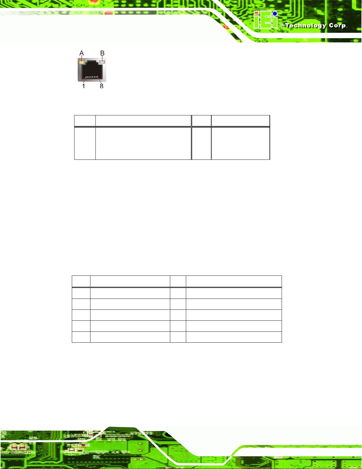
3.3.1 Ethernet Connectors
CN Label: LAN1, LAN2
CN Type:
CN Location:
CN Pinouts:
The WAFER-CV-D25501/N26001 is equipped with two built-in RJ-45 Ethernet controllers.
Each controller can connect to the LAN through one RJ-45 LAN connector.
Pin Description Pin Description
1 LAN1_MDI0+ 5 LAN1_MDI2+
2 LAN1_MDI0- 6 LAN1_MDI23 LAN1_MDI1+ 7 LAN1_MDI3+
4 LAN1_MDI1- 8 LAN1_MDI3-
RJ-45 connector
See Figure 3-21
See Table 3-22
Page 34
Table 3-22: LAN Pinouts
Page 50
WAFER-CV-D25501/N26001 3.5" Motherboard
Figure 3-22: RJ-45 Ethernet Connector
LED Description LED Description
A on: linked
blinking: data is being sent/received
B off: 10 Mb/s
green: 100 Mb/s
orange: 1000 Mb/s
Table 3-23: RJ-45 Ethernet Connector LEDs
3.3.2 Serial Port Connector (COM1)
CN Label: COM1
CN Type:
CN Location:
CN Pinouts:
The serial port connects to a RS-232 serial communications device.
Pin Description Pin Description
1
2
DATA CARRIER DETECT
RECEIVE DATA (
Male DB-9 connector
See Figure 3-21
See Table 3-24 and Figure 3-23
DATA SET READY
(DCD)
RXD)
6
REQUEST TO SEND
7
(DSR)
(RTS)
3
4
5 GND
TRANSMIT DATA
DATA TERMINAL READY
(TXD)
(DTR)
CLEAR TO SEND
8
RING INDICATOR
9
(CTS)
(RI)
Table 3-24: RS-232 Serial Port (COM 1) Pinouts
Page 35
Page 51

Figure 3-23: COM1 Pinout Locations
3.3.3 USB Connectors
CN Label: USB1
WAFER-CV-D25501/N26001 3.5" Motherboard
CN Type:
CN Location:
CN Pinouts:
Dual USB port
See Figure 3-21
See Table 3-25
The ports connect to both USB 2.0 and USB 1.1 devices.
Pin Description Pin Description
1
3 DATA- 4 DATA5 DATA+ 6 DATA+
7 GND 8 GND
USB_VCC
2 USB_VCC
Table 3-25: USB Port Pinouts
3.3.4 VGA Connector
CN Label: VGA1
Page 36
CN Type:
CN Location:
CN Pinouts:
15-pin Female
See Figure 3-21
See Figure 3-24 and Table 3-26
The VGA connector connects to a monitor that accepts a standard VGA input.
Page 52

WAFER-CV-D25501/N26001 3.5" Motherboard
Pin Description Pin Description
1 RED 2 GREEN
3 BLUE 4 NC
5 GND 6 GND
7 GND 8 GND
9 VGAVCC 10 GND
11 NC 12 DDCDAT
13 HSYNC 14 VSYNC
15 DDCCLK
Table 3-26: VGA Connector Pinouts
Figure 3-24: VGA Connector
NOTE:
Due to Intel® GMA driver limitation, the monitor connected to the VGA
connector may become extended desktop or not have signal to it after
restarting from the graphics driver installation. To work out this
limitation, press the Ctrl+Alt+F1 hotkey to switch the primary display to
CRT mode.
Page 37
Page 53

WAFER-CV-D25501/N26001 3.5" Motherboard
Chapter
4
4 Installation
Page 38
Page 54

WAFER-CV-D25501/N26001 3.5" Motherboard
4.1 Anti-static Precautions
WARNING:
Failure to take ESD precautions during the installation of the
WAFER-CV-D25501/N26001 may result in permanent damage to the
WAFER-CV-D25501/N26001 and severe injury to the user.
Electrostatic discharge (ESD) can cause serious damage to electronic components,
including the WAFER-CV-D25501/N26001. Dry climates are especially susceptible to
ESD. It is therefore critical that whenever the WAFER-CV-D25501/N26001 or any other
electrical component is handled, the following anti-static precautions are strictly adhered
to.
Wear an anti-static wristband: - Wearing a simple anti-static wristband can
help to prevent ESD from damaging the board.
Self-grounding:- Before handling the board touch any grounded conducting
material. During the time the board is handled, frequently touch any
conducting materials that are connected to the ground.
Use an anti-static pad: When configuring the W A FER-CV-D25501/N26001,
place it on an antic-static pad. This reduces the possibility of ESD damaging
the WAFER-CV-D25501/N26001.
Only handle the edges of the PCB:-: When handling the PCB, hold the PCB
by the edges.
4.2 Installation Considerations
NOTE:
The following installation notices and installation considerations should
be read and understood before installation. All installation notices must
be strictly adhered to. Failing to adhere to these precautions may lead
to severe damage and injury to the person performing the installation.
Page 39
Page 55

WAFER-CV-D25501/N26001 3.5" Motherboard
WARNING:
The installation instructions described in this manual should be
carefully followed in order to prevent damage to the components and
injury to the user.
Before and during the installation please DO the following:
Read the user manual:
o The user manual provides a complete description of the
WAFER-CV-D25501/N26001 installation instructions and configuration
options.
Wear an electrostatic discharge cuff (ESD):
o Electronic components are easily damaged by ESD. Wearing an ESD cuff
removes ESD from the body and helps prevent ESD damage.
Place the WAFER-CV-D25501/N26001 on an antistatic pad:
o When installing or configuring the motherboard, place it on an antistatic
pad. This helps to prevent potential ESD damage.
Turn all power to the W A FER-CV-D25501/N26001 off:
o When working with the WAFER-CV-D25501/N26001, make sure that it is
disconnected from all power supplies and that no electricity is being fed
into the system.
Before and during the installation of the WAFER-CV-D25501/N26001 DO NOT:
Remove any of the stickers on the PCB board. These stickers are required for
warranty validation.
Use the product before verifying all the cables and power connectors are
properly connected.
Page 40
Allow screws to come in contact with the PCB circuit, connector pins, or its
components.
Page 56

WAFER-CV-D25501/N26001 3.5" Motherboard
4.3 SO-DIMM Installation
WARNING:
Using incorrectly specified SO-DIMM may cause permanent damage to
the WAFER-CV-D25501/N26001. Please make sure the purchased
SO-DIMM complies with the memory specifications of the
WAFER-CV-D25501/N26001. SO-DIMM specifications compliant with
the WAFER-CV-D25501/N26001 are listed in Chapter 1.
To install a SO-DIMM into a SO-DIMM socket, please follow the steps below and refer to
Figure 4-1.
Figure 4-1: SO-DIMM Installation
Step 1: Locate the SO-DIMM socket. Place the WAFER-CV-D25501/N26001 on an
anti-static pad with the solder side facing up.
Step 2: Align the SO-DIMM with the socket. The SO-DIMM must be oriented in such a
way that the notch in the middle of the SO-DIMM must be aligned with the
plastic bridge in the socket.
Step 3: Insert the SO-DIMM. Push the SO-DIMM chip into the socket at an angle. (See
Figure 4-1)
Step 4: Open the SO-DIMM socket arms. Gently pull the arms of the SO-DIMM socket
out and push the rear of the SO-DIMM down. (See
Figure 4-1)
Page 41
Page 57

Step 5: Secure the SO-DIMM. Release the arms on the SO-DIMM socket. They clip into
place and secure the SO-DIMM in the socket.Step 0:
4.4 Jumper Settings
NOTE:
A jumper is a metal bridge used to close
an electrical circuit. It consists of two or
three metal pins and a small metal clip
(often protected by a plastic cover) that
slides over the pins to connect them. To
CLOSE/SHORT a jumper means
connecting the pins of the jumper with
WAFER-CV-D25501/N26001 3.5" Motherboard
the plastic clip and to OPEN a jumper means removing the plastic clip
from a jumper.
The hardware jumpers must be set before installation. Jumpers are shown in Table 4-1.
Description Label Type
AT/ATX power selection JP2 2-pin header
Clear CMOS JP3 3-pin header
LVDS1 voltage selection JP4 3-pin header
LVDS2 voltage selection JP1 3-pin header
LVDS2 panel type selection SW1 4-pin switch
Table 4-1: Jumpers
4.4.1 AT/ATX Power Selection Jumper
Jumper Label: JP2
Page 42
Jumper Type:
Jumper Settings:
Jumper Location:
2-pin header
See Table 4-2
See Figure 4-2
Page 58

WAFER-CV-D25501/N26001 3.5" Motherboard
The AT/ATX power selection jumper specifies the system power mode as AT or ATX.
Setting Description
Short 1-2 Use ATX power (Default)
Off Use AT power
Table 4-2: AT/ATX Power Selection Jumper Settings
Figure 4-2: AT/ATX Power Selection Jumper Location
4.4.2 Clear CMOS Jumper
Jumper Label: JP3
Jumper Type:
Jumper Settings:
Jumper Location:
3-pin header
See Table 4-3
See Figure 4-3
To reset the BIOS, move the jumper to the "Clear BIOS" position for 3 seconds or more,
and then move back to the default position.
Setting Description
Short 1-2 Normal
Short 2-3 Clear BIOS
Table 4-3: Clear CMOS Jumper Settings
Page 43
Page 59
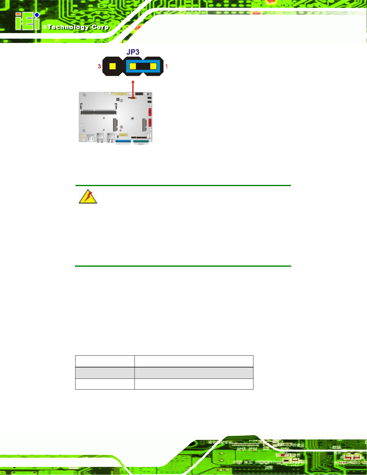
Figure 4-3: Clear CMOS Jumper Location
4.4.3 LVDS1 Voltage Selection
WARNING:
WAFER-CV-D25501/N26001 3.5" Motherboard
Permanent damage to the screen and WAFER-CV-D25501/N26001
may occur if the wrong voltage is selected with this jumper. Please
refer to the user guide that came with the monitor to select the correct
voltage.
Jumper Label: JP4
Jumper Type:
Jumper Settings:
Jumper Location:
Sets the voltage provided to the monitor by LVDS1.
Setting Description
Short 1-2 +3.3V LVDS (Default)
Short 2-3 +5V LVDS
3-pin header
Table 4-4
See
Figure 4-4
See
Page 44
Table 4-4: LVDS1 Voltage Selection Jumper Settings
Page 60

WAFER-CV-D25501/N26001 3.5" Motherboard
Figure 4-4: LVDS1 Voltage Selection Jumper Location
4.4.4 LVDS2 Voltage Selection
WARNING:
Permanent damage to the screen and WAFER-CV-D25501/N26001
may occur if the wrong voltage is selected with this jumper. Please
refer to the user guide that came with the monitor to select the correct
voltage.
Jumper Label: JP1
Jumper Type:
Jumper Settings:
Jumper Location:
Sets the voltage provided to the monitor connected to LVDS2.
Setting Description
Short 1-2 +3.3V LVDS (Default)
Short 2-3 +5V LVDS
3-pin header
Table 4-5
See
Figure 4-5
See
Table 4-5: LVDS2 Voltage Selection Jumper Settings
Page 45
Page 61

WAFER-CV-D25501/N26001 3.5" Motherboard
Figure 4-5: LVDS2 Voltage Selection Jumper Location
4.4.5 LVDS2 Panel Type Selection Jumper
Jumper Label: SW1
Jumper Type:
Jumper Settings:
Jumper Location:
4-pin switch
Table 4-6
See
Figure 4-6
See
Sets the panel type of the LVDS2 video channel.
Pin No.
4321
0000 800 x 600 @ 60 Hz 18-bit Single
0001 1024 x 768 @ 60Hz 18-bit Single
0010 1024 x 768 @ 60Hz 24-bit Single
0011 1280 x 768 @ 60Hz 18-bit Single
0100 1280 x 800 @ 60Hz 18-bit Single
0101 1280 x 960 @ 60Hz 18-bit Single
0110 1280 x 1024 @ 60Hz 24-bit Dual
0111 1366 x 768 @ 60Hz 18-bit Single
1000 1366 x 768 @ 60Hz 24-bit Single
EDID Resolution Color Depth Channel
Page 46
1001 1440 x 900 @ 60Hz 24-bit Dual
1010 1440 x 1050 @ 60Hz 24-bit Dual
1011 1600 x 900 @ 60Hz 24-bit Dual
Page 62
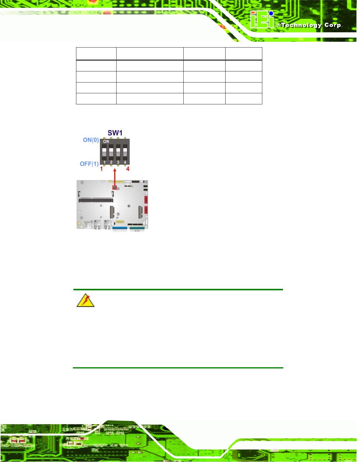
WAFER-CV-D25501/N26001 3.5" Motherboard
Pin No.
4321
1100 1680 x 1050 @ 60Hz 24-bit Dual
1101 1600 x 1200 @ 60Hz 24-bit Dual
1110 1920 x 1080 @ 60Hz 24-bit Dual
1111 1920 x 1200 @ 60Hz 24-bit Dual
Table 4-6: LVDS2 Panel Resolution
EDID Resolution Color Depth Channel
Figure 4-6: LVDS2 Panel Type Selection Switch Location
4.5 Chassis Installation
4.5.1 Airflow
WARNING:
Airflow is critical to the cooling of the CPU and other on-board
components. The chassis in which the WAFER-CV-D25501/N26001
must have air vents to allow cool air to move into the system and hot air
to move out.
The WAFER-CV-D25501/N26001 must be installed in a chassis with ventilation holes on
the sides allowing airflow to travel through the heat sink surface. In a system with an
Page 47
Page 63
WAFER-CV-D25501/N26001 3.5" Motherboard
individual power supply unit, the cooling fan of a power supply can also help generate
airflow through the board surface.
NOTE:
IEI has a wide range of chassis available. Please contact your
WAFER-CV-D25501/N26001 vendor, reseller or an IEI sales
representative at
(
3http://www.ieiworld.com.tw) to find out more about the available
3sales@iei.com.tw or visit the IEI website
chassis.
4.5.2 Motherboard Installation
To install the WAFER-CV-D25501/N26001 motherboard into the chassis please refer to
the reference material that came with the chassis.
4.6 Internal Peripheral Device Connections
This section outlines the installation of peripheral devices to the on-board connectors.
4.6.1 Audio Kit Installation
The Audio Kit that came with the WAFER-CV-D25501/N26001 connects to the 10-pin
audio connector on the WAFER-CV-D25501/N26001. The audio kit consists of three
audio jacks. One audio jack, Mic In, connects to a microphone. The remaining two audio
Page 48
jacks, Line-In and Line-Out, connect to two speakers. To install the audio kit, please refer
to the steps below:
Step 1: Locate the audio connector. The location of the 10-pin audi o connector is
shown in Chapter 3.
Step 2: Align pin 1. Align pin 1 on the on-board connector with pin 1 on the audio kit
connector. Pin 1 on the audio kit connector is indicated with a white dot. See
Figure 4-7.
Page 64

WAFER-CV-D25501/N26001 3.5" Motherboard
Figure 4-7: Audio Kit Cable Connection
Step 3: Connect the audio devices. Connect one speaker to the line-in audio jack, one
speaker to the line-out audio jack and a microphone to the mic-in audio jack.
4.6.2 LVDS LCD Installation
The WAFER-CV-D25501/N26001 can be connected to a TFT LCD screen through the
LVDS crimp connectors on the board. To connect a TFT LCD to the
WAFER-CV-D25501/N26001, please follow the steps below.
Step 1: Locate the connector. The locations of the LVDS connectors are shown in
Chapter 3.
Step 2: Insert the cable connector. Insert the connector from the LVDS PCB driving
board to the LVDS connector as shown in
Figure 4-8. When connecting the
connectors, make sure the pins are properly aligned.
Page 49
Page 65

WAFER-CV-D25501/N26001 3.5" Motherboard
WARNING:
The diagram below is merely for illustration. The configuration and
connection of the cables from the TFT LCD screen being installed may
be different. Please refer to the installation manual that came with the
TFT LCD screen.
Page 50
Figure 4-8: LVDS Connector
Step 3: Locate the backlight inverter connector. The locations of the backlight
inverter connectors are shown in Chapter 3.
Step 4: Connect backlight connector. Connect the backlight connector to the driver
TFT LCD PCB as shown in
make sure the pins are properly aligned.
Figure 4-9. When inserting the cable connector,
Page 66

WAFER-CV-D25501/N26001 3.5" Motherboard
Figure 4-9: Backlight Inverter Connection
4.6.3 Full-size PCIe Mini Card Installation
To install a full-size PCIe Mini card, please follow the steps below.
Step 1: Locate the full-size PCIe Mini card slot. The location of the full-size PCIe Mini
card slot is shown in Chapter 3.
Step 2: Remove the retention screw. Remove the retention screw secured on the
motherboard as shown in
Figure 4-10.
Page 51
Page 67
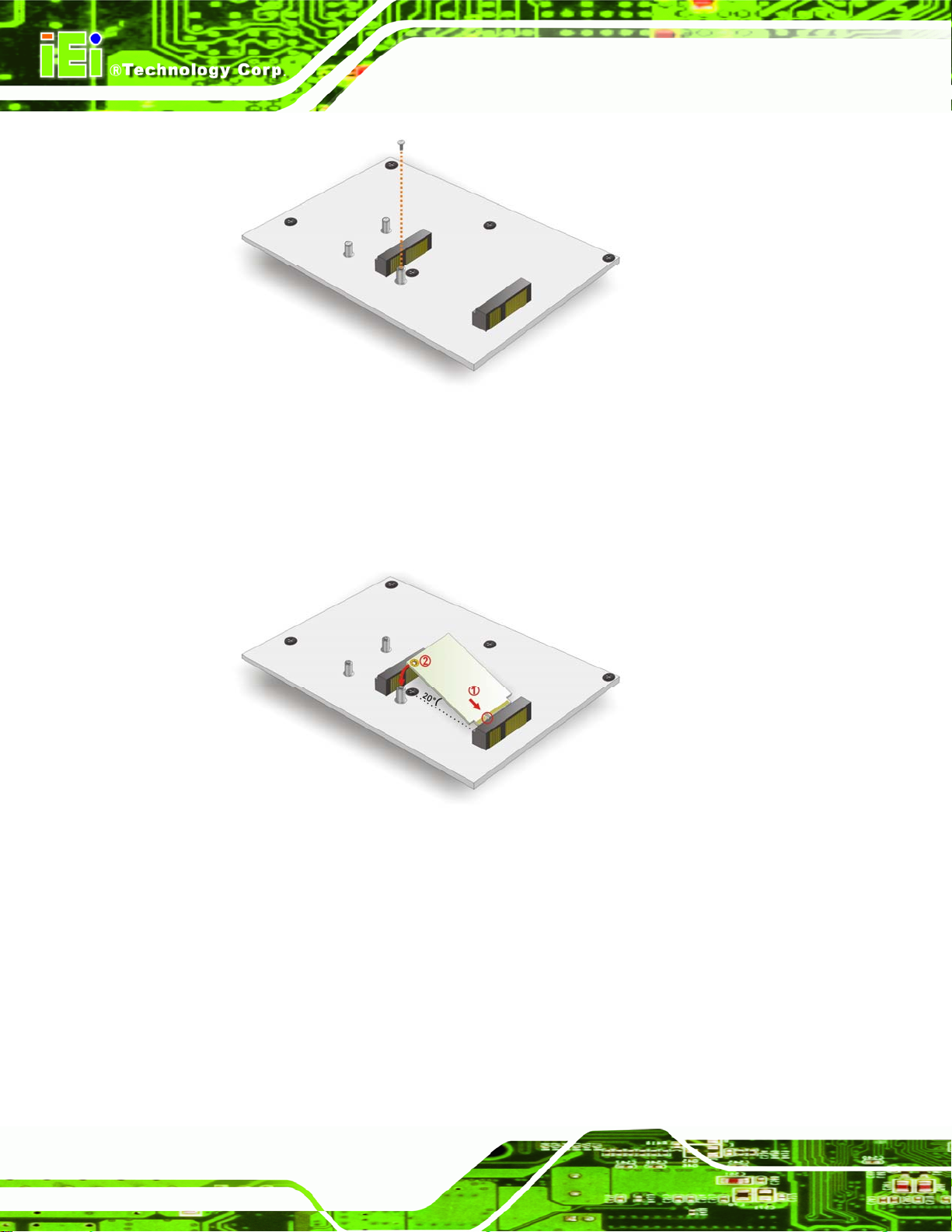
Figure 4-10: Remove the Retention Screw for the Full-size PCIe Mini Card
Step 3: Insert into the socket at an angle. Line up the notch on the card with the notch
on the connector. Slide the PCIe Mini card into the socket at an angle of about
WAFER-CV-D25501/N26001 3.5" Motherboard
Figure 4-11).
20º (
Figure 4-11: Insert the Full-size PCIe Mini Card into the Socket at an Angle
Step 4: Secure the full-size PCIe Mini card. Secure the full-size PCIe Mini card with
the retention screw previously removed (
Figure 4-12).
Page 52
Page 68

WAFER-CV-D25501/N26001 3.5" Motherboard
Figure 4-12: Secure the Full-size PCIe Mini Card
4.6.4 Half-size PCIe Mini Card Installation
To install a half-size PCIe Mini card, please follow the steps below.
Step 1: Locate the half-size PCIe Mini card slot. The location of the half-size PCIe
Mini card slot is shown in Chapter 3.
Step 2: Remove the retention screws. Remove the two retention screws secured on
the motherboard as shown in
Figure 4-13.
Figure 4-13: Remove the Retention Screws for the Half-size PCIe Mini Card
Page 53
Page 69

Step 3: Insert into the socket at an angle. Line up the notch on the card with the notch
on the connector. Slide the PCIe Mini card into the socket at an angle of about
Figure 4-14).
20º (
Figure 4-14: Insert the Half-size PCIe Mini Card into the Socket at an Angle
WAFER-CV-D25501/N26001 3.5" Motherboard
Step 4: Secure the half-size PCIe Mini card. Secure the half-size PCIe Mini card with
the two retention screws previously removed (
Figure 4-15: Secure the Half-size PCIe Mini Card
Figure 4-15).
4.6.5 SATA Drive Connection
Page 54
The WAFER-CV-D25501/N26001 is shipped with a SATA drive cable. To connect the
SATA drive to the connector, please follow the steps below.
Page 70

WAFER-CV-D25501/N26001 3.5" Motherboard
Step 1: Locate the SA TA connector and the SAT A p ower connector. The locations of
the connectors are shown in Chapter 3.
Step 2: Insert the cable connector. Insert the cable connector into the on-board SATA
drive connector and the SATA power connector. See
Figure 4-16.
Figure 4-16: SATA Drive Cable Connection
Step 3: Connect the cable to the SATA disk. Connect the connector on the other end
of the cable to the connector at the back of the SATA drive. See
Step 4: To remove the SATA cable from the SATA connector , press the clip on the
connector at the end of the cable.
4.6.6 Single RS-232 Cable
The single RS-232 cable consists of one serial port connector attached to a serial
communications cable that is then attached to a D-sub 9 male connector. To install the
single RS-232 cable, please follow the steps below.
Figure 4-16.
Page 55
Page 71

Step 1: Locate the connector. The locations of the RS-232 connectors are shown in
Chapter 3.
Step 2: Insert the cable connector. Insert the connector into the serial port header.
Figure 4-17. A key on the front of the cable connector ensures the
See
connector can only be installed in one direction.
WAFER-CV-D25501/N26001 3.5" Motherboard
Figure 4-17: Single RS-232 Cable Installation
Step 3: Secure the bracket. The single RS-232 connector has two retention scre ws
that must be secured to a chassis or bracket.
Step 4: Connect the serial device. Once the single RS-232 connector is connected to
a chassis or bracket, a serial communications device can be connected to the
system.
4.6.7 Keyboard/Mouse Y-cable Connector
The WAFER-CV-D25501/N26001 is shipped with a keyboard/mouse Y-cable connector.
The keyboard/mouse Y-cable connector connects to a keyboard/mouse connector on the
WAFER-CV-D25501/N26001 and branches into two cables that are each connected to a
PS/2 connector, one for a mouse and one for a keyboard. To connect the keyboard/mouse
Y-cable connector, please follow the steps below.
Page 56
Page 72

WAFER-CV-D25501/N26001 3.5" Motherboard
Step 1: Locate the connector. The location of the keyboard/mouse Y-cable connector
is shown in Chapter 3.
Step 2: Align the connectors. Correctly align pin 1 on the cable connector with pin 1 on
the WAFER-CV-D25501/N26001 keyboard/mouse connector. See
Step 3: Insert the cable connectors. Once the cable connector is p rope rly aligne d wit h
the keyboard/mouse connector on the WAFER-CV-D25501/N26001, connect
the cable connector to the on-board connector. See
Figure 4-18.
Figure 4-18.
Figure 4-18: Keyboard/mouse Y-cable Connection
Step 4: Attach PS/2 connectors to the chassis. The keyboard/mouse Y-cable
connector is connected to two PS/2 connectors. To secure the PS/2 connectors
to the chassis please refer to the installation instructions that came with the
chassis.
Step 5: Connect the keyboard and mouse. Once the PS/2 connectors are connected
to the chassis, a keyboard and mouse can each be connected to one of the
Page 57
Page 73

PS/2 connectors. The keyboard PS/2 connector and mouse PS/2 connector are
both marked. Please make sure the keyboard and mouse are connected to the
correct PS/2 connector.
WAFER-CV-D25501/N26001 3.5" Motherboard
4.7 External Peripheral Interface Connection
This section describes connecting devices to the external connectors on the
WAFER-CV-D25501/N26001.
4.7.1 LAN Connection
The RJ-45 connector enables connection to an external network. To connect a LAN cable
with an RJ-45 connector, please follow the instructions below.
Step 1: Locate the RJ-45 connector. The locations of the RJ-45 connectors are shown
in Chapter 3.
Step 2: Align the connectors. Align the RJ-45 connector on the LAN cable with the
RJ-45 connector on the WAFER-CV-D25501/N26001. See
Figure 4-19.
Page 58
Figure 4-19: LAN Connection
Page 74

WAFER-CV-D25501/N26001 3.5" Motherboard
Step 3: Insert the LAN cable RJ-45 connector. Once aligned, gently insert the LAN
cable RJ-45 connector into the on-board RJ-45 connector.
4.7.2 Serial Device Connection
The WAFER-CV-D25501/N26001 has a single male DB-9 connector on the external
peripheral interface panel for a serial device. Follow the steps below to connect a serial
device to the WAFER-CV-D25501/N26001.
Step 1: Locate the DB-9 connector. The location of the DB-9 connector is shown in
Chapter 3.
Step 2: Insert the serial connector. Insert the DB-9 connector of a serial device into
the DB-9 connector on the external peripheral interface. See
Figure 4-20.
Figure 4-20: Serial Device Connector
Step 3: Secure the connector. Secure the serial device connector to the external
interface by tightening the two retention screws on either side of the connector.
Page 59
Page 75

WAFER-CV-D25501/N26001 3.5" Motherboard
4.7.3 USB Connection (Dual Connector)
The external USB Series "A" receptacle connectors provide easier and quicker access to
external USB devices. Follow the steps below to connect USB devices to the
WAFER-CV-D25501/N26001.
Step 1: Locate the USB Series "A" receptacle connectors. The locations of the USB
Series "A" receptacle connectors are shown in Chapter 3.
Step 2: Insert a USB Series "A" plug. Insert the USB Series "A" plug of a device into
the USB Series "A" receptacle on the external peripheral interface. See
Figure 4-21.
Figure 4-21: USB Connector
4.7.4 VGA Monitor Connection
The WAFER-CV-D25501/N26001 has a single female DB-15 connector on the external
peripheral interface panel. The DB-15 connector is connected to a CRT or VGA monitor.
To connect a monitor to the WAFER-CV-D25501/N26001, please follow the instructions
below.
Page 60
Page 76

WAFER-CV-D25501/N26001 3.5" Motherboard
Step 1: Locate the female DB-15 connector. The location of the female DB-15
connector is shown in Chapter 3.
Step 2: Align the VGA connector. Align the male DB-15 connector on the VGA screen
cable with the female DB-15 connector on the external peripheral interface.
Step 3: Insert the VGA connector. Once the conne ctors are prop erly aligned with the
insert the male connector from the VGA screen into the female connector on the
WAFER-CV-D25501/N26001. See
Figure 4-22: VGA Connector
Figure 4-22.
Step 4: Secure the connector. Secure the DB-15 VGA connector from the VGA
monitor to the external interface by tightening the two retention screws on either
side of the connector.
Page 61
Page 77
4.8 Heat Sink Enclosure
WARNING:
Never run the WAFER-CV-D25501/N26001 without the heat sink
secured to the board. The heat sink ensures the system remains cool
and does not need addition heat sinks to cool the system.
WARNING:
When running the WAFER-CV-D25501/N26001, do not put the
WAFER-CV-D25501/N26001 directly on a surface that can not
dissipate system heat, especially the wooden or plastic desk. It is
WAFER-CV-D25501/N26001 3.5" Motherboard
highly recommended to run the WAFER-CV-D25501/N26001
on a heat dissipation surface or
using copper pillars to hold the board up from the desk below
When the WAFER-CV-D25501/N26001 is shipped it is secured to a heat sink with five
retention screws. If the WAFER-CV-D25501/N26001 must be removed from the heat sink,
the five retention screws must be removed.
Page 62
Page 78
WAFER-CV-D25501/N26001 3.5" Motherboard
Figure 4-23: Heat Sink Retention Screws
Page 63
Page 79

WAFER-CV-D25501/N26001 3.5" Motherboard
Chapter
5
5 BIOS
Page 64
Page 80

WAFER-CV-D25501/N26001 3.5" Motherboard
5.1 Introduction
The BIOS is programmed onto the BIOS chip. The BIOS setup program allows changes to
certain system settings. This chapter outlines the options that can be changed.
5.1.1 Starting Setup
The UEFI BIOS is activated when the computer is turned on. The setup program can be
activated in one of two ways.
1. Press the DEL or F2 key as soon as the system is turned on or
2. Press the DEL or F2 key when the “Press DEL or F2 to enter SETUP”
message appears on the screen.
If the message disappears before the DEL or F2 key is pressed, restart the computer and
try again.
5.1.2 Using Setup
Use the arrow keys to highlight items, press ENTER to select, use the PageUp and
PageDown keys to change entries, press F1 for help and press E
keys are shown in the following table.
Key Function
Up arrow Move to previous item
Down arrow Move to next item
Left arrow Move to the item on the left hand side
Right arrow Move to the item on the right hand side
+ Increase the numeric value or make changes
- Decrease the numeric value or make changes
Page Up key Move to the next page
Page Dn key Move to the previous page
SC to quit. Navigation
Page 65
Page 81

Key Function
Esc key Main Menu – Quit and not save changes into CM OS
F1 General help, only for St atus Page Setup Menu and Option
F2 Load previous values
F3 Load optimized defaults
F4 Save changes and Exit BIOS
Table 5-1: BIOS Navigation Keys
5.1.3 Getting Help
WAFER-CV-D25501/N26001 3.5" Motherboard
Status Page Setup Menu and Option Page Setup Menu -Exit current page and return to Main Menu
Page Setup Menu
When F1 is pressed a small help window describing the appropriate keys to use and the
possible selections for the highlighted item appears. To exit the Help Window press E
the F1 key again.
5.1.4 Unable to Reboot after Configuration Changes
If the computer cannot boot after changes to the system configuration are made, CMOS
defaults. Use the jumper described in Chapter 4.
5.1.5 BIOS Menu Bar
The menu bar on top of the BIOS screen has the following main items:
Main – Changes the basic system configuration.
Advanced – Changes the advanced system settings.
Chipset – Changes the chipset settings.
Boot – Changes the system boot configuration.
Security – Sets User and Supervisor Passwords.
SC or
Page 66
Save & Exit – Selects exit options and loads default settings
The following sections completely describe the configuration options found in the menu
items at the top of the BIOS screen and listed above.
Page 82

WAFER-CV-D25501/N26001 3.5" Motherboard
5.2 Main
The Main BIOS menu (BIOS Menu 1) appears when the BIOS Setup program is entered.
The Main menu gives an overview of the basic system information.
Aptio Setup Utility – Copyright (C) 2011 American Megatrends, Inc.
Main Advanced Chipset Boot Security Save & Exit
BIOS Information
BIOS Vendor American Megatrends
Core Version 4.6.5.3 0.16
Compliancy UEFI 2.3; PI 1.2
Project Version B217AR10.ROM
Build Date and Time 03/14/2012 11:53:40
System Date [Fri 04/13/2012]
System Time [15:10:27]
Access Level Administrator
Version 2.14.1219. Copyright (C) 2011 American Megatrends, Inc.
Set the Date. Use Tab to
switch between Data
elements.
----------------------
↑ ↓: Select Item
Enter: Select
+/-: Change Opt.
F1: General Help
F2: Previous Values
F3: Optimized Defaults
F4: Save & Exit
ESC: Exit
: Select Screen
BIOS Menu 1: Main
System Overview
The BIOS Information lists a brief summary of the BIOS. The fields in BIOS Information
cannot be changed. The items shown in the system overview include:
BIOS Vendor: Installed BIOS vendor
Core Version: Current BIOS version
Project Version: the board version
Build Date and Time: Date and time the current BIOS version was made
The System Overview field also has two user configurable fields:
System Date [xx/xx/xx]
Use the System Date option to set the system date. Manually enter the day, month and
year.
Page 67
Page 83

System Time [xx:xx:xx]
Use the System Time option to set the system time. Manually enter the hours, minutes
and seconds.
5.3 Advanced
Use the Advanced menu (BIOS Menu 2) to configure the CPU and peripheral devices
through the following sub-menus:
WARNING:
Setting the wrong values in the sections below may cause the system
to malfunction. Make sure that the settings made are compatible with
the hardware.
WAFER-CV-D25501/N26001 3.5" Motherboard
Aptio Setup Utility – Copyright (C) 2011 American Megatrends, Inc.
Main Advanced Chipset Boot Security Save & Exit
> ACPI Settings
> RTC Wake Settings
> CPU Configuration
> IDE Configuration
> USB Configuration
> F81866 Super IO Configuration
> F81866 H/W Monitor
> Serial Port Console Redirection
> iEi Feature
Version 2.14.1219. Copyright (C) 2011 American Megatrends, Inc.
BIOS Menu 2: Advanced
System ACPI Parameters
----------------------
↑ ↓: Select Item
Enter: Select
+/-: Change Opt.
F1: General Help
F2: Previous Values
F3: Optimized Defaults
F4: Save & Exit
ESC: Exit
5.3.1 ACPI Settings
: Select Screen
Page 68
The ACPI Settings menu (BIOS Menu 3) configures the Advanced Configuration and
Power Interface (ACPI) options.
Page 84

S
WAFER-CV-D25501/N26001 3.5" Motherboard
Aptio Setup Utility – Copyright (C) 2011 American Megatrends, Inc.
Advanced
ACPI Settings
ACPI Sleep State [S1 (CPU Stop Clock)]
Version 2.14.1219. Copyright (C) 2011 American Megatrends, Inc.
elect the highest ACPI
sleep state the system
will enter when the
SUSPEND button is
pressed.
----------------------
: Select Screen
↑ ↓: Select Item
Enter: Select
+/-: Change Opt.
F1: General Help
F2: Previous Values
F3: Optimized Defaults
F4: Save & Exit
ESC: Exit
BIOS Menu 3: ACPI Settings
ACPI Sleep State [S1 (CPU Stop Clock)]
Use the ACPI Sleep State option to specify the sleep state the system enters when it is
not being used.
S1 (CPU Stop
Clock)
S3 (Suspend to
RAM)
DEFAULT
The system enters S1 (POS) sleep state. The
system appears off. The CPU is stopped; RAM is
refreshed; the system is running in a low power
mode.
The caches are flushed and the CPU is powered
off. Power to the RAM is maintained. The
computer returns slower to a working state, but
more power is saved.
5.3.2 RTC Wake Settings
The RTC Wake Settings menu (BIOS Menu 4) enables the system to wake at the
specified time.
Page 69
Page 85

w
Aptio Setup Utility – Copyright (C) 2011 American Megatrends, Inc.
Advanced
Wake system with Fixed Time [Disabled]
Version 2.14.1219. Copyright (C) 2011 American Megatrends, Inc.
WAFER-CV-D25501/N26001 3.5" Motherboard
Enable or disable System
ake on alarm event. When
enabled, System will
wake on the
date::hr::min::sec
specified
----------------------
: Select Screen
↑ ↓: Select Item
Enter: Select
+/-: Change Opt.
F1: General Help
F2: Previous Values
F3: Optimized Defaults
F4: Save & Exit
ESC: Exit
BIOS Menu 4: RTC Wake Settings
Wake system with Fixed Time [Disabled]
Use the Wake system with Fixed Time option to enable or disable the system wake on
alarm event.
Disabled D
Enabled
EFAULT
The real time clock (RTC) cannot generate a wake
event
If selected, the Wake up every day option appears
allowing you to enable to disable the system to wake
every day at the specified time. Besides, the
following options appear with values that can be
selected:
Wake up date
Wake up hour
Wake up minute
Wake up second
After setting the alarm, the computer turns itself on
from a suspend state when the alarm goes off.
Page 70
Page 86

a
T
WAFER-CV-D25501/N26001 3.5" Motherboard
5.3.3 CPU Configuration
Use the CPU Configuration menu (BIOS Menu 5) to view detailed CPU specifications
and configure the CPU.
Aptio Setup Utility – Copyright (C) 2011 American Megatrends, Inc.
Advanced
CPU Configuration
Processor Type Intel(R) Atom(TM)
CPU D2700 @ 2.13GHz
EMT64 Not Supported
Processor Speed 2132 MHz
System Bus Speed 533 MHz
Ratio Status 16
Actual Ratio 16
System Bus Speed 533 MHz
Processor Stepping 30661
Microcode Revision 268
L1 Cache RAM 2x56 k
L2 Cache RAM 2x512 k
Processor Core Dual
Hyper-Threading Supported
Hyper-Threading [Enabled]
Version 2.14.1219. Copyright (C) 2011 American Megatrends, Inc.
Enabled for Windows XP
nd Linux (OS optimized
for Hyper-Threading
echnology) and Disabled
for other OS (OS not
optimized for
Hyper-Threading
Technology).
----------------------
: Select Screen
↑ ↓: Select Item
Enter: Select
+/-: Change Opt.
F1: General Help
F2: Previous Values
F3: Optimized Defaults
F4: Save & Exit
ESC: Exit
BIOS Menu 5: CPU Configuration
The CPU Configuration menu (
Processor Type: Lists the brand name of the CPU being used.
EMT64: Indicates if EMT64 is supported by the CPU.
Processor Speed: Lists the CPU processing speed.
System Bus Speed: Lists the system bus speed.
Ratio Status: Lists the ratio status.
Actual Ratio: Lists the ratio of the frequency to the clock speed.
Processor Stepping: Lists the CPU ID.
Microcode Revision: Lists the microcode revision.
L1 Cache RAM: Lists the CPU L1 cache size.
L2 Cache RAM: Lists the CPU L2 cache size.
Processor Core: Lists the number of the processor core.
Hyper-Threading: Indicates if Intel HT Technology is supported by the CPU.
BIOS Menu 5) lists the following CPU details:
Page 71
Page 87

Hyper-Threading [Enabled]
Use the Hyper-Threading BIOS option to enable or disable the Intel Hyper-Threading
Technology.
WAFER-CV-D25501/N26001 3.5" Motherboard
Disabled
Enabled DEFAULT
Disables the Intel Hyper-Threading Technology.
Enables the Intel Hyper-Threading Technology.
5.3.4 IDE Configuration
Use the IDE Configuration menu (BIOS Menu 6) to change and/or set the configuration
of the SATA devices installed in the system.
Aptio Setup Utility – Copyright (C) 2011 American Megatrends, Inc.
Advanced
SATA1 Not Present
SATA2 Not Present
Configure SATA as [IDE]
Version 2.14.1219. Copyright (C) 2011 American Megatrends, Inc.
Select a configuration
for SATA Controller.
---------------------
: Select Screen
↑ ↓: Select Item
Enter: Select
+/-: Change Opt.
F1: General Help
F2: Previous Values
F3: Optimized Defaults
F4: Save & Exit
ESC: Exit
BIOS Menu 6: IDE Configuration
Configure SATA as [IDE]
Use the Configure SATA as option to configure SATA devices as normal IDE or AHCI
devices.
IDE DEFAULT
AHCI
Page 72
Configures SATA devices as normal IDE device.
Configures SATA devices as AHCI device.
Page 88

d
WAFER-CV-D25501/N26001 3.5" Motherboard
5.3.5 USB Configuration
Use the USB Configuration menu (BIOS Menu 7) to read USB configuration information
and configure the USB settings.
Aptio Setup Utility – Copyright (C) 2011 American Megatrends, Inc.
Advanced
USB Configuration
USB Devices:
None
Legacy USB Support [Enabled]
Version 2.14.1219. Copyright (C) 2011 American Megatrends, Inc.
Enables Legacy USB
support. AUTO option
isables legacy support
if no USB devices are
connected. DISABLE
option will keep USB
devices available only
for EFI applications.
---------------------
: Select Screen
↑ ↓: Select Item
Enter: Select
+/-: Change Opt.
F1: General Help
F2: Previous Values
F3: Optimized Defaults
F4: Save & Exit
ESC: Exit
BIOS Menu 7: USB Configuration
Legacy USB Support [Enabled]
Use the Legacy USB Support BIOS option to enable USB mouse and USB keyboard
support.
Normally if this option is not enabled, any attached USB mouse or USB keyboard does not
become available until a USB compatible operating system is fully booted with all USB
drivers loaded. When this option is enabled, any attached USB mouse or USB keyboard
can control the system even when there is no USB driver loaded onto the system.
Disabled
Enabled DEFAULT
Auto
Legacy USB support disabled
Legacy USB support enabled
Legacy USB support disabled if no USB devices are
connected
Page 73
Page 89

S
E
WAFER-CV-D25501/N26001 3.5" Motherboard
5.3.6 F81866 Super IO Configuration
Use the F81866 Super IO Configuration menu (BIOS Menu 8) to set or change the
configurations for the serial ports.
Aptio Setup Utility – Copyright (C) 2011 American Megatrends, Inc.
Advanced
F81866 Super IO Configuration
F81866 Super IO Chip F81866
> Serial Port 1 Configuration
> Serial Port 2 Configuration
> Serial Port 3 Configuration
> Serial Port 4 Configuration
Version 2.14.1219. Copyright (C) 2011 American Megatrends, Inc.
et Parameters of Serial
Port 1 (COMA)
---------------------
: Select Screen
↑ ↓: Select Item
Enter: Select
+/-: Change Opt.
F1: General Help
F2: Previous Values
F3: Optimized Defaults
F4: Save & Exit
ESC: Exit
BIOS Menu 8: Super IO Configuration
5.3.6.1 Serial Port n Configuration
Use the Serial Port n Configuration menu (BIOS Menu 9) to configure the serial port n.
Aptio Setup Utility – Copyright (C) 2011 American Megatrends, Inc.
Advanced
Serial Port n Configuration
Serial Port [Enabled]
Device Settings IO=3F8h; IRQ=4
Change Settings [Auto]
Version 2.14.1219. Copyright (C) 2011 American Megatrends, Inc.
nable or Disable Serial
Port (COM)
---------------------
: Select Screen
↑ ↓: Select Item
Enter: Select
+/-: Change Opt.
F1: General Help
F2: Previous Values
F3: Optimized Defaults
F4: Save & Exit
ESC: Exit
BIOS Menu 9: Serial Port n Configuration Menu
Page 74
Page 90

WAFER-CV-D25501/N26001 3.5" Motherboard
5.3.6.1.1 Serial Port 1 Configuration
Serial Port [Enabled]
Use the Serial Port option to enable or disable the serial port.
Disabled
Enabled DEFAULT
Change Settings [Auto]
Use the Change Settings option to change the serial port IO port address and interrupt
address.
Auto DEFAULT
IO=3F8h;
IRQ=4
IO=3F8h;
IRQ=3, 4
IO=2F8h;
IRQ=3, 4
Disable the serial port
Enable the serial port
The serial port IO port address and interrupt address
are automatically detected.
Serial Port I/O port address is 3F8h and the interrupt
address is IRQ4
Serial Port I/O port address is 3F8h and the interrupt
address is IRQ3, 4
Serial Port I/O port address is 2F8h and the interrupt
address is IRQ3, 4
IO=3E8h;
IRQ=3, 4
IO=2E8h;
IRQ=3, 4
5.3.6.1.2 Serial Port 2 Configuration
Serial Port [Enabled]
Use the Serial Port option to enable or disable the serial port.
Disabled
Enabled DEFAULT
Serial Port I/O port address is 3E8h and the interrupt
address is IRQ3, 4
Serial Port I/O port address is 2E8h and the interrupt
address is IRQ3, 4
Disable the serial port
Enable the serial port
Page 75
Page 91

Change Settings [Auto]
Use the Change Settings option to change the serial port IO port address and interrupt
address.
WAFER-CV-D25501/N26001 3.5" Motherboard
Auto DEFAULT
IO=2F8h;
IRQ=3
IO=3F8h;
IRQ=3, 4
IO=2F8h;
IRQ=3, 4
IO=3E8h;
IRQ=3, 4
IO=2E8h;
IRQ=3, 4
The serial port IO port address and interrupt address
are automatically detected.
Serial Port I/O port address is 2F8h and the interrupt
address is IRQ3
Serial Port I/O port address is 3F8h and the interrupt
address is IRQ3, 4
Serial Port I/O port address is 2F8h and the interrupt
address is IRQ3, 4
Serial Port I/O port address is 3E8h and the interrupt
address is IRQ3, 4
Serial Port I/O port address is 2E8h and the interrupt
address is IRQ3, 4
5.3.6.1.3 Serial Port 3 Configuration
Serial Port [Enabled]
Use the Serial Port option to enable or disable the serial port.
Disabled
Enabled DEFAULT
Change Settings [Auto]
Use the Change Settings option to change the serial port IO port address and interrupt
address.
Auto DEFAULT
Page 76
Disable the serial port
Enable the serial port
The serial port IO port address and interrupt address
are automatically detected.
Page 92

WAFER-CV-D25501/N26001 3.5" Motherboard
IO=3E8h;
IRQ=10
IO=3F8h;
IRQ=10, 11
IO=2F8h;
IRQ=10, 11
IO=3E8h;
IRQ=10, 11
IO=2E8h;
IRQ=10, 11
IO=250h;
IRQ=10, 11
IO=2E0h;
IRQ=10, 11
Serial Port I/O port address is 3E8h and the interrupt
address is IRQ10
Serial Port I/O port address is 3F8h and the interrupt
address is IRQ10, 11
Serial Port I/O port address is 2F8h and the interrupt
address is IRQ10, 11
Serial Port I/O port address is 3E8h and the interrupt
address is IRQ10, 11
Serial Port I/O port address is 2E8h and the interrupt
address is IRQ10, 11
Serial Port I/O port address is 250h and the interrupt
address is IRQ10, 11
Serial Port I/O port address is 2E0h and the interrupt
address is IRQ10, 11
5.3.6.1.4 Serial Port 4 Configuration
Serial Port [Enabled]
Use the Serial Port option to enable or disable the serial port.
Disabled
Enabled DEFAULT
Change Settings [Auto]
Use the Change Settings option to change the serial port IO port address and interrupt
address.
Auto DEFAULT
IO=2E8h;
Disable the serial port
Enable the serial port
The serial port IO port address and interrupt address
are automatically detected.
Serial Port I/O port address is 2E8h and the interrupt
IRQ=10
address is IRQ10
Page 77
Page 93
WAFER-CV-D25501/N26001 3.5" Motherboard
IO=3F8h;
IRQ=10, 11
IO=2F8h;
IRQ=10, 11
IO=3E8h;
IRQ=10, 11
IO=2E8h;
IRQ=10, 11
IO=250h;
IRQ=10, 11
IO=2E0h;
IRQ=10, 11
5.3.7 F81866 H/W Monitor
Serial Port I/O port address is 3F8h and the interrupt
address is IRQ10, 11
Serial Port I/O port address is 2F8h and the interrupt
address is IRQ10, 11
Serial Port I/O port address is 3E8h and the interrupt
address is IRQ10, 11
Serial Port I/O port address is 2E8h and the interrupt
address is IRQ10, 11
Serial Port I/O port address is 250h and the interrupt
address is IRQ10, 11
Serial Port I/O port address is 2E0h and the interrupt
address is IRQ10, 11
The F81866 H/W Monitor menu (BIOS Menu 10) contains the fan configuration
submenus and displays operating temperature, fan speeds and system voltages.
Aptio Setup Utility – Copyright (C) 2011 American Megatrends, Inc.
Advanced
PC Health Status
> Smart Fan Mode Configuration
CPU Temperature : +52 C
System Temperature : +51 C
CPU_FAN1 Speed : N/A
SYS_FAN1 Speed : N/A
+VCC_CPU : +1.488 V
+VCC_GFX : +0.968 V
+V1.05S : +1.056 V
+V1.5_DDR3 : +1.504 V
VSB5V : +5.040 V
+V3.3S : +3.344 V
VSB3V : +3.344 V
VBAT : +3.264 V
Version 2.14.1219. Copyright (C) 2011 American Megatrends, Inc.
BIOS Menu 10: F81866 H/W Monitor
Smart Fan Mode Select
---------------------
: Select Screen
↑ ↓: Select Item
Enter: Select
+/-: Change Opt.
F1: General Help
F2: Previous Values
F3: Optimized Defaults
F4: Save & Exit
ESC: Exit
Page 78
Page 94

WAFER-CV-D25501/N26001 3.5" Motherboard
PC Health Status
The following system parameters and values are shown. The system parameters that are
monitored are:
System Temperatures:
o CPU Temperature
o System Temperature
Fan Speeds:
o CPU Fan Speed
o System Fan Speed
Voltages:
o +VCC_CPU
o +VCC_GFX
o +V1.05S
o +1.5_DDR3
o VSB5V
o +V3.3S
o VSB3V
o VBAT
5.3.7.1 Smart Fan Mode Configuration
Use the Smart Fan Mode Configuration submenu (BIOS Menu 11) to configure fan
temperature and speed settings.
Page 79
Page 95
Aptio Setup Utility – Copyright (C) 2011 American Megatrends, Inc.
Advanced
Smart Fan Mode Configuration
CPU_FAN1 Smart Fan Control [Auto Duty-Cycle Mode]
CPU Temperature 1 60
CPU Temperature 2 50
CPU Temperature 3 40
CPU Temperature 4 30
SYS_FAN1 Smart Fan Control [Auto Duty-Cycle Mode]
System Temperature 1 60
System Temperature 2 50
System Temperature 3 40
System Temperature 4 30
Version 2.14.1219. Copyright (C) 2011 American Megatrends, Inc.
BIOS Menu 11: Smart Fan Mode Configuration
CPU_FAN1/SYS_FAN Smart Fan Control [Auto Duty-Cycle Mode]
WAFER-CV-D25501/N26001 3.5" Motherboard
Smart Fan Mode Select
---------------------
: Select Screen
↑ ↓: Select Item
Enter: Select
+/-: Change Opt.
F1: General Help
F2: Previous Values
F3: Optimized Defaults
F4: Save & Exit
ESC: Exit
Use the CPU_FAN1 or SYS_FAN1 Smart Fan Control option to configure the CPU or
System Smart Fan.
Auto
Duty-Cycle
Mode
Manual Duty
Mode
CPU/System Temperature n
Use the + or – key to change the fan CPU or System Temperature n value. Enter a
decimal number between 1 and 100.
D
EFAULT
The fan adjusts its speed using Auto Duty-Cycle
settings
The fan spins at the speed set in Manual Duty
Mode settings
5.3.8 Serial Port Console Redirection
The Serial Port Console Redirection menu (BIOS Menu 12) allows the console
redirection options to be configured. Console redirection allows users to maintain a
Page 80
system remotely by re-directing keyboard input and text output through the serial port.
Page 96

WAFER-CV-D25501/N26001 3.5" Motherboard
Aptio Setup Utility – Copyright (C) 2011 American Megatrends, Inc.
Advanced
COM1
Console Redirection [Disabled]
> Console Redirection Settings
COM2
Console Redirection [Disabled]
> Console Redirection Settings
COM3
Console Redirection [Disabled]
> Console Redirection Settings
Version 2.14.1219. Copyright (C) 2011 American Megatrends, Inc.
BIOS Menu 12: Serial Port Console Redirection
Console Redirection
Enable or Disable
---------------------
: Select Screen
↑ ↓: Select Item
Enter: Select
+/-: Change Opt.
F1: General Help
F2: Previous Values
F3: Optimized Defaults
F4: Save & Exit
ESC: Exit
Console Redirection [Disabled]
Use Console Redirection option to enable or disable the console redirection fun ction.
Disabled DEFAULT
Enabled
Terminal Type [ANSI]
Use the Terminal Type option to specify the remote terminal type.
VT100
VT100+
VT-UTF8
ANSI DEFAULT
Bits per second [115200]
Disabled the console redirection function
Enabled the console redirection function
The target terminal type is VT100
The target terminal type is VT100+
The target terminal type is VT-UTF8
The target terminal type is ANSI
Use the Bits per second option to specify the serial port transmission speed. The speed
must match the other side. Long or noisy lines may require lower speeds.
Page 81
Page 97

WAFER-CV-D25501/N26001 3.5" Motherboard
9600
19200
38400
57600
115200 DEFAULT
Data Bits [8]
Use the Data Bits option to specify the number of data bits.
7
8 DEFAULT
Parity [None]
Use the Parity option to specify the parity bit that can be sent with the data bits for
Sets the serial port transmission speed at 9600.
Sets the serial port transmission speed at 19200.
Sets the serial port transmission speed at 38400.
Sets the serial port transmission speed at 57600.
Sets the serial port transmission speed at 115200.
Sets the data bits at 7.
Sets the data bits at 8.
detecting the transmission errors.
None DEFAULT
Even
Odd
Mark
Space
Stop Bits [1]
Use the Stop Bits option to specify the number of stop bits used to indicate the end of a
serial data packet. Communication with slow devices may require more than 1 stop bit.
No parity bit is sent with the data bits.
The parity bit is 0 if the number of ones in the data
bits is even.
The parity bit is 0 if the number of ones in the data
bits is odd.
The parity bit is always 1. This option does not
provide error detection.
The parity bit is always 0. This option does not
provide error detection.
Page 82
Page 98

c
s
WAFER-CV-D25501/N26001 3.5" Motherboard
1 DEFAULT
2
Sets the number of stop bits at 1.
Sets the number of stop bits at 2.
5.3.9 iEi Feature
Use the iEi Feature menu (BIOS Menu 13) to configure One Key Recovery function.
Aptio Setup Utility – Copyright (C) 2011 American Megatrends, Inc.
Advanced
iEi Feature
Auto Recovery Function [Disabled]
Version 2.14.1219. Copyright (C) 2011 American Megatrends, Inc.
Auto Recovery Function
Reboot and recover
system automatically
within 10 min, when OS
rashes. Please install
Auto Recovery API
ervice before enabling
this function.
---------------------
: Select Screen
↑ ↓: Select Item
Enter: Select
+/-: Change Opt.
F1: General Help
F2: Previous Values
F3: Optimized Defaults
F4: Save & Exit
ESC: Exit
BIOS Menu 13: IEI Feature
Auto Recovery Function [Disabled]
Use the Auto Recovery Function BIOS option to enable or disable the auto recovery
function of the IEI One Key Recovery.
Disabled DEFAULT
Enabled
Auto recovery function disabled
Auto recovery function enabled
Page 83
Page 99

WAFER-CV-D25501/N26001 3.5" Motherboard
5.4 Chipset
Use the Chipset menu (BIOS Menu 14) to access the Host Bridge and Southbridge
configuration menus.
WARNING!
Setting the wrong values for the Chipset BIOS selections in the Chipset BIOS menu
may cause the system to malfunction.
Aptio Setup Utility – Copyright (C) 2011 American Megatrends, Inc.
Main Advanced Chipset Boot Security Save & Exit
> Host Bridge
> South Bridge
Host Bridge Parameters
---------------------
↑ ↓: Select Item
Enter: Select
+/-: Change Opt.
F1: General Help
F2: Previous Values
F3: Optimized Defaults
F4: Save & Exit
ESC: Exit
: Select Screen
Version 2.14.1219. Copyright (C) 2011 American Megatrends, Inc.
BIOS Menu 14: Chipset
5.4.1 Host Bridge Configuration
Use the Host Bridge Configuration menu (BIOS Menu 15) to configure the Intel IGD
Configuration and display the memory information.
Page 84
Page 100

S
w
d
WAFER-CV-D25501/N26001 3.5" Motherboard
Aptio Setup Utility – Copyright (C) 2011 American Megatrends, Inc.
Chipset
> Intel IGD Configuration
******* Memory Information *******
Memory Frequency 1067 MHz(DDR3)
Total Memory 1024 MB
DIMM#1 1024 MB
Version 2.14.1219. Copyright (C) 2011 American Megatrends, Inc.
BIOS Menu 15: Host Bridge Configuration
Config Intel IGD
Settings
---------------------
: Select Screen
↑ ↓: Select Item
Enter: Select
+/-: Change Opt.
F1: General Help
F2: Previous Values
F3: Optimized Defaults
F4: Save & Exit
ESC: Exit
5.4.1.1 Intel IGD Configuration
Use the Intel IGD Configuration submenu (BIOS Menu 16) to configure the video device
connected to the system.
Aptio Setup Utility – Copyright (C) 2011 American Megatrends, Inc.
Advanced
Intel IGD Configuration
IGFX – Boot Type [VBIOS Default]
LVDS1 Panel Type [800x600 LVDS]
Backlight Control [Inverted]
Fixed Graphics Memory Size [128MB]
Version 2.14.1219. Copyright (C) 2011 American Megatrends, Inc.
elect the Video Device
hich will be activated
uring POST. This has no
effect if external
graphics present.
: Select Screen
↑ ↓: Select Item
Enter: Select
+/-: Change Opt.
F1: General Help
F2: Previous Values
F3: Optimized Defaults
F4: Save & Exit
ESC: Exit
BIOS Menu 16: Intel IGD Configuration
Page 85
 Loading...