

查询MK3807-01RI供应商
DATASHEET
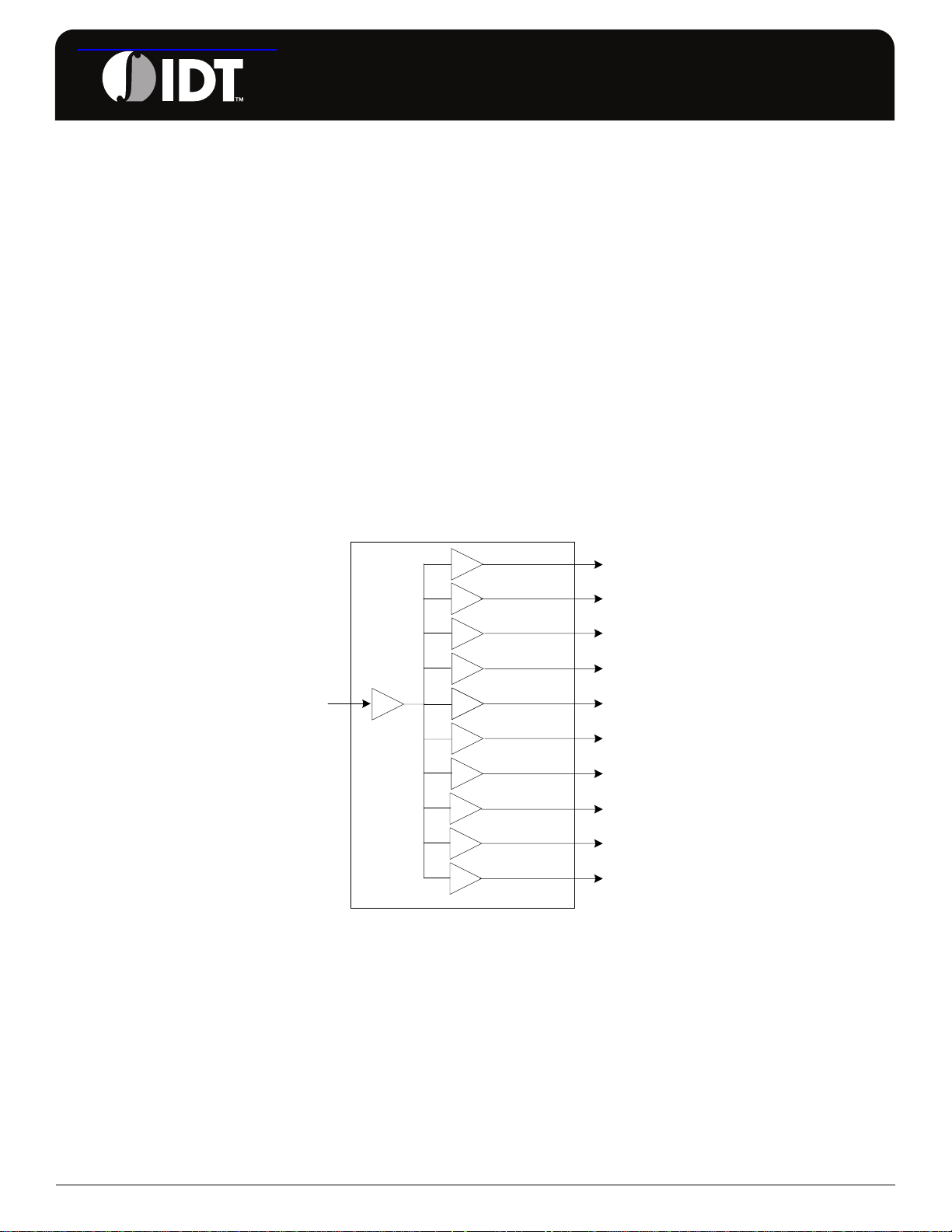
BUFFER/CLOCK DRIVER MK3807-01
Description
The MK3807-01 is a low skew 3.3 V, 1 to 10 fanout buffer.
The large fanout from a single input line reduces loading on
the input clock. The TTL level outputs reduce noise levels on
the part. Typical applications are clock and signal
distribution.
Block Diagram
Features
• Packaged in 20-pin SSOP
• Available in Pb (lead) free package
• 1 to 10 fanout buffer
• Maximum skew between outputs of same package 0.35
ns
• Maximum skew between outputs of different packages
0.75 ns
• Max propagation delay of 3.8 ns
• Operating voltage of 3.3 V
• Advanced, low power, CMOS process
• Industrial temperature range -40° C to +85° C
• Hysteresis on all inputs
CLK1
CLK2
CLK3
IN
CLK4
CLK5
CLK6
CLK7
CLK8
CLK9
CLK10
IDT™ / ICS™
BUFFER/CLOCK DRIVER 1
MK3807-01 REV D 060407
MK3807-01
BUFFER/CLOCK DRIVER FAN OUT BUFFER
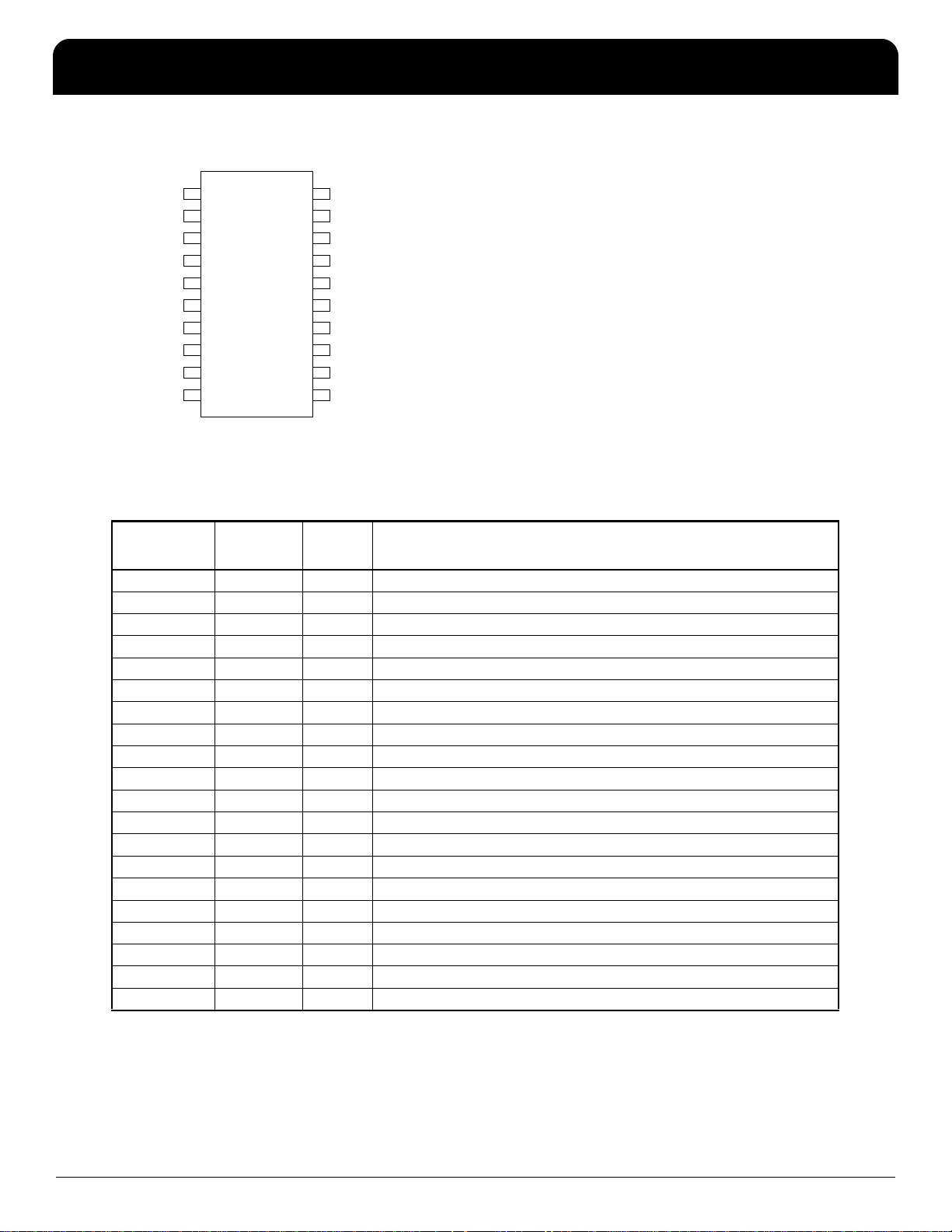
Pin Assignment
1IN
GND CLK10
VDD GND
CLK2
GND
CLK3
VDD
CLK4 CLK6
GND
2
3CLK1
4
5
7
8
9
10
20 pin SOIC, SSOP, TSSOP
Pin Descriptions
Pin
Number
1 IN Input Clock input.
2 GND Power Connect to ground.
3 CLK1 Output Clock output.
4 VDD Power Connect to +3.3 V.
5 CLK2 Output Clock output.
6 GND Power Connect to ground.
7 CLK3 Output Clock output.
8 VDD Power Connect to +3.3 V.
9 CLK4 Output Clock output.
10 GND Power Connect to ground.
11 CLK5 Output Clock output.
12 CLK6 Output Clock output.
13 GND Power Connect to ground.
14 CLK7 Output Clock output.
15 VDD Power Connect to +3.3 V.
16 CLK8 Output Clock output.
17 GND Power Connect to ground.
18 CLK9 Output Clock output.
19 CLK10 Output Clock output.
20 VDD Power Connect to +3.3 V.
Pin
Name
20
19
18 CLK9
17
16
156
14
13
12
11
VDD
CLK8
VDD
CLK7
GND
CLK5
Pin
Type
Pin Description
IDT™ / ICS™
BUFFER/CLOCK DRIVER 2
MK3807-01 REV D 060407
MK3807-01
BUFFER/CLOCK DRIVER FAN OUT BUFFER
External Components
The MK3807-01 requires a minimum number of external
components for proper operation.
Decoupling Capacitors
Decoupling capacitors of 0.01µF must be connected
between VDD and GND, as close to these pins as possible.
For optimum device performance, the decoupling capacitors
should be mounted on the component side of the PCB.
Avoid the use of vias in the decoupling circuit.
Series Termination Resistor
When the PCB trace between the clock outputs and the
loads are over 1 inch, series termination should be used. To
series terminate a 50Ω trace (a commonly used trace
impedance) place a 33Ω resistor in series with the clock
line, as close to the clock output pin as possible. The
nominal impedance of the clock output is 20Ω.
PCB Layout Recommendations
For optimum device performance and lowest output phase
noise, the following guidelines should be observed.
1) The 0.01µF decoupling capacitors should be mounted on
the component side of the board as close to the VDD pins
as possible. No vias should be used between the
decoupling capacitors and VDD pins. The PCB trace to VDD
pin should be kept as short as possible, as should the PCB
trace to the ground via.
2) To minimize EMI, the 33Ω series termination resistor, (if
needed) should be placed close to the clock output.
Absolute Maximum Ratings
Stresses above the ratings listed below can cause permanent damage to the MK3807-01. These ratings, which are
standard values for IDT commercially rated parts, are stress ratings only. Functional operation of the device at these
or any other conditions above those indicated in the operational sections of the specifications is not implied.
Exposure to absolute maximum rating conditions for extended periods can affect product reliability. Electrical
parameters are guaranteed only over the recommended operating temperature range.
Item Rating
Supply Voltage, VDD 7 V
All Inputs and Outputs -0.5 V to VDD+0.5 V
Ambient Operating Temperature -40 to +85°C
Storage Temperature -65 to +150°C
Junction Temperature 125°C
Soldering Temperature 260°C
Recommended Operation Conditions
Parameter Min. Typ. Max. Units
Ambient Operating Temperature -40 +85 °C
Power Supply Voltage (measured in respect to GND) +3.135 +3.3 +3.465 V
IDT™ / ICS™
BUFFER/CLOCK DRIVER 3
MK3807-01 REV D 060407

MK3807-01
BUFFER/CLOCK DRIVER FAN OUT BUFFER
DC Electrical Characteristics
Unless stated otherwise, VDD = 3.3 V ±5%, Ambient Temperature -40° C to +85° C
Parameter Symbol Conditions Min. Typ. Max. Units
Operating Voltage VDD 3.135 3.3 3.465 V
Quiescent Power Supply
Current
Input High Voltage V
Input Low Voltage V
Output High Voltage V
Output Low Voltage V
Short Circuit Current I
Input Capacitance CIN VIN=0V, Note1 5 6.0 pF
Output Capacitance COUT V
Input Hysteresis VH 150 mV
ICC VCC=Max
VIN=GND or VCC
VCC=Max
VIN=@TTL HIGH
(VCC-0.6 V)
High Level Input pins 2 5.5 V
IH
Low Level Input pins -0.5 0.8 V
IL
OH
VCC=min
VIN=VIH or VIL
I
= -0.1 mA,
OH
I
= -8 mA
OH
OL
VCC=min
VIN=VIH or VIL
I
= -0.1 mA,
OL
Io
=16 mA
L
Io
=24 mA
L
OS
VCC=Max,
V
=GND
OUT
=0V, Note1 5.5 8.0 pF
OUT
330µA
2.0 300 µA
VDD-0.2
2.4 3.0
0.2
0.4
0.5
-60 -135 -240 mA
V
V
IDT™ / ICS™
Note1: This parameter is not tested.
BUFFER/CLOCK DRIVER 4
MK3807-01 REV D 060407

MK3807-01
BUFFER/CLOCK DRIVER FAN OUT BUFFER
AC Electrical Characteristics
Unless stated otherwise, VDD = 3.3 V ±5%, Ambient Temperature -40° C to +85° C
Parameter Symbol Conditions Min. Typ. Max. Units
Skew between outputs of same
package
Skew between opposite
transitions of same output
Propagation Delay IN to ON tpLH/tpHL CL=50 pF,
Skew between outputs of
different package at same
power supply, temperature and
speed grade
Output Rise Time
0.8 V to 2.0 V
Output Fall Time
2.0 V to 0.8 V
Duty Cycle
Measured at VDD/2
Test Frequency 1 100 MHz
tsk
9=(0)
CL=50 pF,
RL=500Ω
tsk
(p)
CL=50 pF,
RL=500Ω
RL=500Ω
tsk
(t)
CL=50 pF,
RL=500Ω
tr
(o)
CL=50 pF,
RL=500Ω
tf
(o)
CL=50 pF,
RL=500Ω
DC CL=50 pF,
RL=500Ω
0.35 ns
0.35 ns
1.5 3.8 ns
0.75 ns
1.5 ns
1.5 ns
45 55 %
IDT™ / ICS™
BUFFER/CLOCK DRIVER 5
MK3807-01 REV D 060407

MK3807-01
BUFFER/CLOCK DRIVER FAN OUT BUFFER
Package Outline and Package Dimensions (20-pin SSOP, 150Mil. Body)
Package dimensions are kept current with JEDEC Publication No. 95
INDEX
AREA
20
Symbol Min Max Min Max
Millimeters Inches*
A 1.351.75.053.069
A1 0.10 0.25 .0040 .010
E1
E
A2 -- 1.50 -- .059
b 0.20 0.30 0.008 0.012
C 0.180.25.007.010
D 8.558.75.337.344
E 5.806.20.228.244
1 2
E1 3.80 4.00 .150 .157
e 0.635 Basic 0.025 Basic
D
L 0.401.27.016.050
α 0° 8° 0° 8°
*For reference only. Controlling dimensions in mm.
A
2
A
A
1
c
- C -
e
b
SEATING
.10 (.004)
PLANE
C
L
Ordering Information
Part / Order Number Marking Shipping Packaging Package Temperature
MK3807-01RI MK3807-01RI Tubes 20-pin SSOP -40 to +85° C
MK3807-01RITR MK3807-01RI Tape and Reel 20-pin SSOP -40 to +85° C
MK3807-01RILF 3807-01RILF Tubes 20-pin SSOP -40 to +85° C
MK3807-01RILFTR 3807-01RILF Tape and Reel 20-pin SSOP -40 to +85° C
Parts that are ordered with a “LF” suffix to the part number are the Pb-Free configuration and are RoHS compliant.
While the information presented herein has been checked for both accuracy and reliability, Integrated Device Technology (IDT) assumes
no responsibility for either its use or for the infringement of any patents or other rights of third parties, which would result from its use. No
other circuits, patents, or licenses are implied. This product is intended for use in normal commercial applications. Any other applications
such as those requiring extended temperature range, high reliability, or other extraordinary environmental requirements are not
recommended without additional processing by IDT. IDT reserves the right to change any circuitry or specifications without notice. IDT
does not authorize or warrant any IDT product for use in life support devices or critical medical instruments.
IDT™ / ICS™
BUFFER/CLOCK DRIVER 6
MK3807-01 REV D 060407

MK3807-01
BUFFER/CLOCK DRIVER FAN OUT BUFFER
Innovate with IDT and accelerate your future networks. Contact:
www.IDT.com
For Sales
800-345-7015
408-284-8200
Fax: 408-284-2775
Corporate Headquarters
Integrated Device Technology, Inc.
www.idt.com
© 2006 Integrated Device Technology, Inc. All rights reserved. Product specifications subject to change without notice. IDT an d the IDT logo are trademarks of Integrated Device
Technology, Inc. Accelerated Thinking is a service mark of Integrated Devi ce Technology, Inc. All other brands, product names and marks are or may be trademarks or registered
trademarks used to identify products or services of their respective owners.
Printed in USA
For Tech Support
408-284-4522
www.idt.com/go/clockhelp
 Loading...